WO2024038674A1 - イットリウム質保護膜およびその製造方法ならびに部材 - Google Patents
イットリウム質保護膜およびその製造方法ならびに部材 Download PDFInfo
- Publication number
- WO2024038674A1 WO2024038674A1 PCT/JP2023/022986 JP2023022986W WO2024038674A1 WO 2024038674 A1 WO2024038674 A1 WO 2024038674A1 JP 2023022986 W JP2023022986 W JP 2023022986W WO 2024038674 A1 WO2024038674 A1 WO 2024038674A1
- Authority
- WO
- WIPO (PCT)
- Prior art keywords
- protective film
- yttrium
- film
- base material
- forming surface
- Prior art date
- Legal status (The legal status is an assumption and is not a legal conclusion. Google has not performed a legal analysis and makes no representation as to the accuracy of the status listed.)
- Ceased
Links
Images



Classifications
-
- H—ELECTRICITY
- H10—SEMICONDUCTOR DEVICES; ELECTRIC SOLID-STATE DEVICES NOT OTHERWISE PROVIDED FOR
- H10P—GENERIC PROCESSES OR APPARATUS FOR THE MANUFACTURE OR TREATMENT OF DEVICES COVERED BY CLASS H10
- H10P72/00—Handling or holding of wafers, substrates or devices during manufacture or treatment thereof
- H10P72/70—Handling or holding of wafers, substrates or devices during manufacture or treatment thereof for supporting or gripping
- H10P72/76—Handling or holding of wafers, substrates or devices during manufacture or treatment thereof for supporting or gripping using mechanical means, e.g. clamps or pinches
- H10P72/7604—Handling or holding of wafers, substrates or devices during manufacture or treatment thereof for supporting or gripping using mechanical means, e.g. clamps or pinches the wafers being placed on a susceptor, stage or support
- H10P72/7616—Handling or holding of wafers, substrates or devices during manufacture or treatment thereof for supporting or gripping using mechanical means, e.g. clamps or pinches the wafers being placed on a susceptor, stage or support characterised by a coating, a hardness or a material
-
- C—CHEMISTRY; METALLURGY
- C23—COATING METALLIC MATERIAL; COATING MATERIAL WITH METALLIC MATERIAL; CHEMICAL SURFACE TREATMENT; DIFFUSION TREATMENT OF METALLIC MATERIAL; COATING BY VACUUM EVAPORATION, BY SPUTTERING, BY ION IMPLANTATION OR BY CHEMICAL VAPOUR DEPOSITION, IN GENERAL; INHIBITING CORROSION OF METALLIC MATERIAL OR INCRUSTATION IN GENERAL
- C23C—COATING METALLIC MATERIAL; COATING MATERIAL WITH METALLIC MATERIAL; SURFACE TREATMENT OF METALLIC MATERIAL BY DIFFUSION INTO THE SURFACE, BY CHEMICAL CONVERSION OR SUBSTITUTION; COATING BY VACUUM EVAPORATION, BY SPUTTERING, BY ION IMPLANTATION OR BY CHEMICAL VAPOUR DEPOSITION, IN GENERAL
- C23C14/00—Coating by vacuum evaporation, by sputtering or by ion implantation of the coating forming material
- C23C14/06—Coating by vacuum evaporation, by sputtering or by ion implantation of the coating forming material characterised by the coating material
- C23C14/08—Oxides
-
- C—CHEMISTRY; METALLURGY
- C01—INORGANIC CHEMISTRY
- C01F—COMPOUNDS OF THE METALS BERYLLIUM, MAGNESIUM, ALUMINIUM, CALCIUM, STRONTIUM, BARIUM, RADIUM, THORIUM, OR OF THE RARE-EARTH METALS
- C01F17/00—Compounds of rare earth metals
- C01F17/20—Compounds containing only rare earth metals as the metal element
- C01F17/206—Compounds containing only rare earth metals as the metal element oxide or hydroxide being the only anion
- C01F17/218—Yttrium oxides or hydroxides
-
- C—CHEMISTRY; METALLURGY
- C23—COATING METALLIC MATERIAL; COATING MATERIAL WITH METALLIC MATERIAL; CHEMICAL SURFACE TREATMENT; DIFFUSION TREATMENT OF METALLIC MATERIAL; COATING BY VACUUM EVAPORATION, BY SPUTTERING, BY ION IMPLANTATION OR BY CHEMICAL VAPOUR DEPOSITION, IN GENERAL; INHIBITING CORROSION OF METALLIC MATERIAL OR INCRUSTATION IN GENERAL
- C23C—COATING METALLIC MATERIAL; COATING MATERIAL WITH METALLIC MATERIAL; SURFACE TREATMENT OF METALLIC MATERIAL BY DIFFUSION INTO THE SURFACE, BY CHEMICAL CONVERSION OR SUBSTITUTION; COATING BY VACUUM EVAPORATION, BY SPUTTERING, BY ION IMPLANTATION OR BY CHEMICAL VAPOUR DEPOSITION, IN GENERAL
- C23C14/00—Coating by vacuum evaporation, by sputtering or by ion implantation of the coating forming material
- C23C14/02—Pretreatment of the material to be coated
- C23C14/024—Deposition of sublayers, e.g. to promote adhesion of the coating
-
- C—CHEMISTRY; METALLURGY
- C23—COATING METALLIC MATERIAL; COATING MATERIAL WITH METALLIC MATERIAL; CHEMICAL SURFACE TREATMENT; DIFFUSION TREATMENT OF METALLIC MATERIAL; COATING BY VACUUM EVAPORATION, BY SPUTTERING, BY ION IMPLANTATION OR BY CHEMICAL VAPOUR DEPOSITION, IN GENERAL; INHIBITING CORROSION OF METALLIC MATERIAL OR INCRUSTATION IN GENERAL
- C23C—COATING METALLIC MATERIAL; COATING MATERIAL WITH METALLIC MATERIAL; SURFACE TREATMENT OF METALLIC MATERIAL BY DIFFUSION INTO THE SURFACE, BY CHEMICAL CONVERSION OR SUBSTITUTION; COATING BY VACUUM EVAPORATION, BY SPUTTERING, BY ION IMPLANTATION OR BY CHEMICAL VAPOUR DEPOSITION, IN GENERAL
- C23C14/00—Coating by vacuum evaporation, by sputtering or by ion implantation of the coating forming material
- C23C14/06—Coating by vacuum evaporation, by sputtering or by ion implantation of the coating forming material characterised by the coating material
- C23C14/08—Oxides
- C23C14/083—Oxides of refractory metals or yttrium
-
- C—CHEMISTRY; METALLURGY
- C23—COATING METALLIC MATERIAL; COATING MATERIAL WITH METALLIC MATERIAL; CHEMICAL SURFACE TREATMENT; DIFFUSION TREATMENT OF METALLIC MATERIAL; COATING BY VACUUM EVAPORATION, BY SPUTTERING, BY ION IMPLANTATION OR BY CHEMICAL VAPOUR DEPOSITION, IN GENERAL; INHIBITING CORROSION OF METALLIC MATERIAL OR INCRUSTATION IN GENERAL
- C23C—COATING METALLIC MATERIAL; COATING MATERIAL WITH METALLIC MATERIAL; SURFACE TREATMENT OF METALLIC MATERIAL BY DIFFUSION INTO THE SURFACE, BY CHEMICAL CONVERSION OR SUBSTITUTION; COATING BY VACUUM EVAPORATION, BY SPUTTERING, BY ION IMPLANTATION OR BY CHEMICAL VAPOUR DEPOSITION, IN GENERAL
- C23C14/00—Coating by vacuum evaporation, by sputtering or by ion implantation of the coating forming material
- C23C14/22—Coating by vacuum evaporation, by sputtering or by ion implantation of the coating forming material characterised by the process of coating
-
- C—CHEMISTRY; METALLURGY
- C23—COATING METALLIC MATERIAL; COATING MATERIAL WITH METALLIC MATERIAL; CHEMICAL SURFACE TREATMENT; DIFFUSION TREATMENT OF METALLIC MATERIAL; COATING BY VACUUM EVAPORATION, BY SPUTTERING, BY ION IMPLANTATION OR BY CHEMICAL VAPOUR DEPOSITION, IN GENERAL; INHIBITING CORROSION OF METALLIC MATERIAL OR INCRUSTATION IN GENERAL
- C23C—COATING METALLIC MATERIAL; COATING MATERIAL WITH METALLIC MATERIAL; SURFACE TREATMENT OF METALLIC MATERIAL BY DIFFUSION INTO THE SURFACE, BY CHEMICAL CONVERSION OR SUBSTITUTION; COATING BY VACUUM EVAPORATION, BY SPUTTERING, BY ION IMPLANTATION OR BY CHEMICAL VAPOUR DEPOSITION, IN GENERAL
- C23C14/00—Coating by vacuum evaporation, by sputtering or by ion implantation of the coating forming material
- C23C14/22—Coating by vacuum evaporation, by sputtering or by ion implantation of the coating forming material characterised by the process of coating
- C23C14/221—Ion beam deposition
-
- C—CHEMISTRY; METALLURGY
- C23—COATING METALLIC MATERIAL; COATING MATERIAL WITH METALLIC MATERIAL; CHEMICAL SURFACE TREATMENT; DIFFUSION TREATMENT OF METALLIC MATERIAL; COATING BY VACUUM EVAPORATION, BY SPUTTERING, BY ION IMPLANTATION OR BY CHEMICAL VAPOUR DEPOSITION, IN GENERAL; INHIBITING CORROSION OF METALLIC MATERIAL OR INCRUSTATION IN GENERAL
- C23C—COATING METALLIC MATERIAL; COATING MATERIAL WITH METALLIC MATERIAL; SURFACE TREATMENT OF METALLIC MATERIAL BY DIFFUSION INTO THE SURFACE, BY CHEMICAL CONVERSION OR SUBSTITUTION; COATING BY VACUUM EVAPORATION, BY SPUTTERING, BY ION IMPLANTATION OR BY CHEMICAL VAPOUR DEPOSITION, IN GENERAL
- C23C14/00—Coating by vacuum evaporation, by sputtering or by ion implantation of the coating forming material
- C23C14/22—Coating by vacuum evaporation, by sputtering or by ion implantation of the coating forming material characterised by the process of coating
- C23C14/24—Vacuum evaporation
-
- C—CHEMISTRY; METALLURGY
- C23—COATING METALLIC MATERIAL; COATING MATERIAL WITH METALLIC MATERIAL; CHEMICAL SURFACE TREATMENT; DIFFUSION TREATMENT OF METALLIC MATERIAL; COATING BY VACUUM EVAPORATION, BY SPUTTERING, BY ION IMPLANTATION OR BY CHEMICAL VAPOUR DEPOSITION, IN GENERAL; INHIBITING CORROSION OF METALLIC MATERIAL OR INCRUSTATION IN GENERAL
- C23C—COATING METALLIC MATERIAL; COATING MATERIAL WITH METALLIC MATERIAL; SURFACE TREATMENT OF METALLIC MATERIAL BY DIFFUSION INTO THE SURFACE, BY CHEMICAL CONVERSION OR SUBSTITUTION; COATING BY VACUUM EVAPORATION, BY SPUTTERING, BY ION IMPLANTATION OR BY CHEMICAL VAPOUR DEPOSITION, IN GENERAL
- C23C14/00—Coating by vacuum evaporation, by sputtering or by ion implantation of the coating forming material
- C23C14/22—Coating by vacuum evaporation, by sputtering or by ion implantation of the coating forming material characterised by the process of coating
- C23C14/24—Vacuum evaporation
- C23C14/28—Vacuum evaporation by wave energy or particle radiation
-
- C—CHEMISTRY; METALLURGY
- C23—COATING METALLIC MATERIAL; COATING MATERIAL WITH METALLIC MATERIAL; CHEMICAL SURFACE TREATMENT; DIFFUSION TREATMENT OF METALLIC MATERIAL; COATING BY VACUUM EVAPORATION, BY SPUTTERING, BY ION IMPLANTATION OR BY CHEMICAL VAPOUR DEPOSITION, IN GENERAL; INHIBITING CORROSION OF METALLIC MATERIAL OR INCRUSTATION IN GENERAL
- C23C—COATING METALLIC MATERIAL; COATING MATERIAL WITH METALLIC MATERIAL; SURFACE TREATMENT OF METALLIC MATERIAL BY DIFFUSION INTO THE SURFACE, BY CHEMICAL CONVERSION OR SUBSTITUTION; COATING BY VACUUM EVAPORATION, BY SPUTTERING, BY ION IMPLANTATION OR BY CHEMICAL VAPOUR DEPOSITION, IN GENERAL
- C23C14/00—Coating by vacuum evaporation, by sputtering or by ion implantation of the coating forming material
- C23C14/22—Coating by vacuum evaporation, by sputtering or by ion implantation of the coating forming material characterised by the process of coating
- C23C14/48—Ion implantation
-
- C—CHEMISTRY; METALLURGY
- C23—COATING METALLIC MATERIAL; COATING MATERIAL WITH METALLIC MATERIAL; CHEMICAL SURFACE TREATMENT; DIFFUSION TREATMENT OF METALLIC MATERIAL; COATING BY VACUUM EVAPORATION, BY SPUTTERING, BY ION IMPLANTATION OR BY CHEMICAL VAPOUR DEPOSITION, IN GENERAL; INHIBITING CORROSION OF METALLIC MATERIAL OR INCRUSTATION IN GENERAL
- C23C—COATING METALLIC MATERIAL; COATING MATERIAL WITH METALLIC MATERIAL; SURFACE TREATMENT OF METALLIC MATERIAL BY DIFFUSION INTO THE SURFACE, BY CHEMICAL CONVERSION OR SUBSTITUTION; COATING BY VACUUM EVAPORATION, BY SPUTTERING, BY ION IMPLANTATION OR BY CHEMICAL VAPOUR DEPOSITION, IN GENERAL
- C23C16/00—Chemical coating by decomposition of gaseous compounds, without leaving reaction products of surface material in the coating, i.e. chemical vapour deposition [CVD] processes
- C23C16/44—Chemical coating by decomposition of gaseous compounds, without leaving reaction products of surface material in the coating, i.e. chemical vapour deposition [CVD] processes characterised by the method of coating
- C23C16/4401—Means for minimising impurities, e.g. dust, moisture or residual gas, in the reaction chamber
- C23C16/4404—Coatings or surface treatment on the inside of the reaction chamber or on parts thereof
-
- C—CHEMISTRY; METALLURGY
- C23—COATING METALLIC MATERIAL; COATING MATERIAL WITH METALLIC MATERIAL; CHEMICAL SURFACE TREATMENT; DIFFUSION TREATMENT OF METALLIC MATERIAL; COATING BY VACUUM EVAPORATION, BY SPUTTERING, BY ION IMPLANTATION OR BY CHEMICAL VAPOUR DEPOSITION, IN GENERAL; INHIBITING CORROSION OF METALLIC MATERIAL OR INCRUSTATION IN GENERAL
- C23C—COATING METALLIC MATERIAL; COATING MATERIAL WITH METALLIC MATERIAL; SURFACE TREATMENT OF METALLIC MATERIAL BY DIFFUSION INTO THE SURFACE, BY CHEMICAL CONVERSION OR SUBSTITUTION; COATING BY VACUUM EVAPORATION, BY SPUTTERING, BY ION IMPLANTATION OR BY CHEMICAL VAPOUR DEPOSITION, IN GENERAL
- C23C16/00—Chemical coating by decomposition of gaseous compounds, without leaving reaction products of surface material in the coating, i.e. chemical vapour deposition [CVD] processes
- C23C16/44—Chemical coating by decomposition of gaseous compounds, without leaving reaction products of surface material in the coating, i.e. chemical vapour deposition [CVD] processes characterised by the method of coating
- C23C16/50—Chemical coating by decomposition of gaseous compounds, without leaving reaction products of surface material in the coating, i.e. chemical vapour deposition [CVD] processes characterised by the method of coating using electric discharges
-
- C—CHEMISTRY; METALLURGY
- C25—ELECTROLYTIC OR ELECTROPHORETIC PROCESSES; APPARATUS THEREFOR
- C25D—PROCESSES FOR THE ELECTROLYTIC OR ELECTROPHORETIC PRODUCTION OF COATINGS; ELECTROFORMING; APPARATUS THEREFOR
- C25D11/00—Electrolytic coating by surface reaction, i.e. forming conversion layers
- C25D11/02—Anodisation
- C25D11/04—Anodisation of aluminium or alloys based thereon
- C25D11/18—After-treatment, e.g. pore-sealing
-
- H—ELECTRICITY
- H01—ELECTRIC ELEMENTS
- H01J—ELECTRIC DISCHARGE TUBES OR DISCHARGE LAMPS
- H01J37/00—Discharge tubes with provision for introducing objects or material to be exposed to the discharge, e.g. for the purpose of examination or processing thereof
- H01J37/32—Gas-filled discharge tubes
- H01J37/32431—Constructional details of the reactor
- H01J37/32458—Vessel
- H01J37/32477—Vessel characterised by the means for protecting vessels or internal parts, e.g. coatings
- H01J37/32495—Means for protecting the vessel against plasma
-
- H—ELECTRICITY
- H10—SEMICONDUCTOR DEVICES; ELECTRIC SOLID-STATE DEVICES NOT OTHERWISE PROVIDED FOR
- H10P—GENERIC PROCESSES OR APPARATUS FOR THE MANUFACTURE OR TREATMENT OF DEVICES COVERED BY CLASS H10
- H10P14/00—Formation of materials, e.g. in the shape of layers or pillars
- H10P14/60—Formation of materials, e.g. in the shape of layers or pillars of insulating materials
-
- H—ELECTRICITY
- H10—SEMICONDUCTOR DEVICES; ELECTRIC SOLID-STATE DEVICES NOT OTHERWISE PROVIDED FOR
- H10P—GENERIC PROCESSES OR APPARATUS FOR THE MANUFACTURE OR TREATMENT OF DEVICES COVERED BY CLASS H10
- H10P50/00—Etching of wafers, substrates or parts of devices
- H10P50/20—Dry etching; Plasma etching; Reactive-ion etching
- H10P50/24—Dry etching; Plasma etching; Reactive-ion etching of semiconductor materials
- H10P50/242—Dry etching; Plasma etching; Reactive-ion etching of semiconductor materials of Group IV materials
Definitions
- the present invention relates to a yttrium protective film, its manufacturing method, and members.
- the surface of a semiconductor substrate is microfabricated in a chamber by dry etching using halogen-based gas plasma, or the inside of the chamber from which the semiconductor substrate is taken out after dry etching is exposed to oxygen. Cleaning using gas plasma.
- the members exposed to the plasma in the chamber corrode, and the corroded parts may fall off in the form of particles from the corroded members.
- the fallen particles may become foreign substances that adhere to the semiconductor substrate and cause defects in the circuit.
- Patent Document 1 discloses a thermal spray coating containing yttrium oxide that is formed by thermal spraying.
- the appearance of the yttrium protective film is defective (for example, the yttrium protective film has cracks or wrinkles). In this case, depending on the application, it is not suitable to use the yttrium protective film as it is.
- the present invention was made in view of the above points, and an object of the present invention is to provide a yttrium protective film that is excellent in plasma resistance and appearance.
- the present invention provides the following [1] to [22].
- [1] A yttrium-based protective film containing yttrium oxide, having a porosity of less than 0.5% by volume, and a Vickers hardness of 800 HV or more.
- [2] The yttrium protective film according to [1] above, having a thickness of 0.3 ⁇ m or more.
- [3] The yttrium protective film according to [1] or [2] above, having a thickness of 15 ⁇ m or less.
- [4] The yttrium protective film according to any one of [1] to [3] above, having a crystallite size of 40 nm or less.
- a member comprising a base material and the yttrium protective film according to any one of [1] to [8] above, which is disposed on the film-forming surface that is the surface of the base material.
- the base material is made of at least one member selected from the group consisting of carbon, ceramics, and metals, and the ceramic is made of glass, quartz, aluminum oxide, aluminum nitride, cordierite, yttrium oxide, silicon carbide, and Si.
- the metal is at least one selected from the group consisting of impregnated silicon carbide, silicon nitride, Sialon, and aluminum oxynitride, and the metal is at least one selected from the group consisting of aluminum and aluminum-containing alloys.
- One or more underlayers are provided between the base material and the yttrium protective film, and the underlayers include Al 2 O 3 , SiO 2 , Y 2 O 3 , MgO, ZrO 2 , Any of the above [9] to [15], containing at least one oxide selected from the group consisting of La 2 O 3 , Nd 2 O 3 , Yb 2 O 3 , Eu 2 O 3 and Gd 2 O 3 Components described in Crab.
- the base material has a first film-forming surface that defines a maximum length as the film-forming surface, and a second film-forming surface that is different from the first film-forming surface, and The angle formed by the film formation surface and the second film formation surface is 20° to 120°, and the ratio of the area of the second film formation surface to the total area of the film formation surface is 60% or less, The member according to any one of [9] to [17] above.
- FIG. 2 is a schematic diagram showing an example of a member.
- FIG. 2 is a schematic diagram showing a ring-shaped base material with half thereof cut away. It is a schematic diagram which shows a part of cross section of another ring-shaped base material. It is a schematic diagram which shows a part of cross section of yet another ring-shaped base material.
- FIG. 2 is a schematic diagram showing an apparatus used for manufacturing a yttrium-based protective film.
- 1 is an XRD pattern of the yttrium-based protective film of Example 1.
- 2 is a SEM photograph of the surface of the yttrium protective film of Example 1.
- 1 is a cross-sectional SEM photograph of the yttrium protective film of Example 1.
- the yttrium-based protective film of this embodiment contains yttrium oxide, has a porosity of less than 0.5% by volume, and has a Vickers hardness of 800 HV or more.
- the yttrium-based protective film will also be referred to simply as a "protective film”, and the yttrium-based protective film (protective film) of this embodiment will also be referred to as “main protective film”.
- This protective film has excellent plasma resistance and appearance.
- the present protective film will be explained in more detail below.
- the Vickers hardness of the present protective film is 800 HV or more, preferably 1000 HV or more, more preferably 1100 HV or more, even more preferably 1200 HV or more, particularly preferably 1250 HV or more, Most preferably 1300HV or higher.
- the Vickers hardness of the present protective film is, for example, 1800 HV or less, preferably 1600 HV or less.
- the protective film by the method described below (this manufacturing method).
- the Vickers hardness of the protective film is determined in accordance with JIS Z 2244. More specifically, the Vickers hardness of the present protective film was determined by applying a test force of 0.049 N using a micro Vickers hardness tester (HM-220, manufactured by Mitutoyo) with a diamond indenter with a facing angle of 136°. This is the Vickers hardness (HV0.005) that is sometimes required.
- HM-220 manufactured by Mitutoyo
- the porosity of the present protective film is less than 0.5 volume %, preferably 0.3 volume % or less, and more preferably 0.2 volume % or less, because the plasma resistance and appearance of the present protective film are excellent. , more preferably 0.1% by volume or less.
- the protective film by the method described below (this manufacturing method).
- the porosity of the protective film is determined as follows. First, using a focused ion beam (FIB), slope processing is performed on the protective film and a part of the base material (described later) at an angle of 52° from the surface of the protective film toward the base material. to expose the cross section. The exposed cross section is observed using a field emission scanning electron microscope (FE-SEM) at a magnification of 20,000 times, and an image of the cross section is photographed. Cross-sectional images are taken at multiple locations. Specifically, for example, when the protective film and the base material are circular, one point in the center of the surface of the protective film (or the surface of the base material) and four points located 10 mm apart from the outer periphery.
- FIB focused ion beam
- Photographs were taken at a total of five points, and the size of the cross-sectional image was 6 ⁇ m ⁇ 5 ⁇ m.
- the thickness of the protective film is 5 ⁇ m or more
- cross-sectional images are taken at a plurality of photographing locations so that the entire cross-section of the protective film can be observed in the thickness direction.
- image analysis software ImageJ, manufactured by National Institute of Health
- the ratio of the area of the pores to the area of the entire cross section of the protective film is calculated, and this is regarded as the porosity (unit: volume %) of the protective film. Note that for pores that are too fine to be detected by image analysis software (pores with a pore diameter of 20 nm or less), the area is considered to be 0.
- This protective film contains yttrium oxide (Y 2 O 3 ).
- the Y 2 O 3 content of the present protective film is preferably 95% by mass or more, more preferably 98% by mass or more, and even more preferably 100% by mass.
- the protective film manufactured by the method described below (this manufacturing method) is substantially made of only Y 2 O 3 , and the Y 2 O 3 content thereof satisfies the above range.
- the degree of orientation of the (222) plane of Y 2 O 3 in the protective film (hereinafter referred to as (also simply referred to as "degree of orientation") is preferably higher. Specifically, the degree of orientation is preferably 50% or more, more preferably 65% or more, and even more preferably 80% or more. In order to keep the degree of orientation within the above range, it is preferable to manufacture the protective film by the method described below (this manufacturing method).
- the degree of orientation is the ratio (unit: %) of the peak intensity of the (222) plane when the sum of the peak intensities of each plane of Y 2 O 3 is 100 in the XRD pattern of the protective film (see Figure 6). be.
- the XRD pattern of the protective film is obtained by performing XRD measurement using an X-ray diffraction device (D8 DISCOVER Plus, manufactured by Bruker) under the following conditions in minute part 2D (two-dimensional) mode.
- ⁇ X-ray source CuK ⁇ ray (output: 45kV, current: 120mA)
- ⁇ Scanning range: 2 ⁇ 10° to 80°
- ⁇ Step time 0.2s/step
- ⁇ Scan speed 10°/min
- Step width 0.02°
- ⁇ Detector Multi-mode detector EIGER (2D mode)
- ⁇ Incidence side optical system Multilayer film mirror + 1.0mm ⁇ microslit + 1.0mm ⁇ collimator
- the crystallite size of the present protective film is preferably 40 nm or less, more preferably 30 nm or less, even more preferably 20 nm or less, even more preferably 15 nm or less, particularly preferably 11 nm or less, even more preferably 10 nm or less, and 9 nm or less. is very preferable, and most preferably 8 nm or less.
- the crystallite size of the present protective film is preferably 2 nm or more, more preferably 6 nm or more, and even more preferably 7 nm or more.
- the crystallite size in the protective film is determined using the Scherrer equation based on XRD pattern data obtained by XRD measurement of the mirror-polished protective film.
- the thickness of the protective film is, for example, 0.3 ⁇ m or more, preferably 1.0 ⁇ m or more, more preferably 1.5 ⁇ m or more, even more preferably 5 ⁇ m or more, particularly preferably 10 ⁇ m or more, and most preferably 15 ⁇ m or more.
- the thickness of the present protective film is, for example, 300 ⁇ m or less, preferably 200 ⁇ m or less, more preferably 100 ⁇ m or less, even more preferably 50 ⁇ m or less, and particularly preferably 30 ⁇ m or less.
- the thickness of this protective film may be 10 ⁇ m or less.
- the thickness of the protective film is measured as follows. Observe the cross section of the protective film using a scanning electron microscope (SEM), measure the thickness of the protective film at five arbitrary points, and calculate the average value of the five measured points as the thickness of the protective film (unit: : ⁇ m).
- SEM scanning electron microscope
- the number of hydrogen atoms in this protective film is small. Thereby, the plasma resistance of the present protective film is further improved.
- the reason for this is presumed to be as follows. That is, when there is a large amount of hydrogen in the protective film, this hydrogen tends to react with fluorine contained in plasma (or gas used to generate plasma), and as a result, the protective film is easily damaged. On the other hand, if there is less hydrogen in the protective film, the reaction with fluorine will be relatively reduced, and damage to the protective film will be suppressed.
- the number of hydrogen atoms in the present protective film is preferably 5.0 ⁇ 10 21 atoms/cm 3 or less, more preferably 4.5 ⁇ 10 21 atoms/cm 3 or less, It is more preferably 3.5 ⁇ 10 21 pieces/cm 3 or less, even more preferably 3.0 ⁇ 10 21 pieces/cm 3 or less, particularly preferably 2.5 ⁇ 10 21 pieces/cm 3 or less, and 2.3 ⁇
- the most preferable number is 10 21 pieces/cm 3 or less.
- the hydrogen in the protective film is due to the influence of water contained in the base material, which will be described later.
- the material of the base material is ceramic
- the number of hydrogen atoms in the formed protective film can be reduced by heating the base material (preheating) before forming the protective film. Other methods for reducing the number of hydrogen atoms in the protective film will be described later.
- the number of hydrogen atoms in the protective film is preferably 0.1 ⁇ 10 21 /cm 3 or more, more preferably 0.5 ⁇ 10 21 /cm 3 or more.
- the number of hydrogen atoms in the protective film was determined using a secondary ion mass spectrometer (model IMS-6f, manufactured by Ametek) under the following conditions: primary ion species Cs + , primary acceleration voltage 15.0 kV, detection area ⁇ 8 ⁇ m, measurement depth 500 nm. Find it with
- the stress (intra-film stress, residual stress) of the present protective film is preferably compressive stress rather than tensile stress.
- the compressive stress of the present protective film is preferably 100 MPa or more, more preferably 200 MPa or more, and even more preferably 300 MPa or more.
- the compressive stress of the protective film is preferably 1,700 MPa or less, more preferably 1,600 MPa or less, and even more preferably 1,500 MPa or less.
- the compressive stress of the protective film is determined as follows.
- a protective film was formed on a quartz glass substrate, and the surface shape of the formed protective film was measured using a surface shape measuring device (Surfcom NEX 241 SD2-13, manufactured by Tokyo Seimitsu Co., Ltd.) using Stoney's formula (the following formula). ), find the compressive stress (film stress ⁇ ) of the protective film. Stoney's equation is expressed as follows.
- ⁇ Yd 2 /6(1- ⁇ )t ⁇ 8h/c 2 +4h2
- ⁇ film stress
- Y Young's modulus of the substrate
- d thickness of the substrate
- ⁇ Poisson's ratio of the substrate
- t thickness of the protective film
- h amount of warpage
- c radius of curvature.
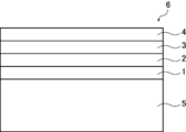
- FIG. 1 is a schematic diagram showing an example of the member 6.
- the member 6 has a base material 5 and a yttrium protective film 4.
- a base layer (base layer 1, base layer 2, and base layer 3) may be disposed between the base material 5 and the yttrium protective film 4.
- the base layer is not limited to three layers.
- the member of this embodiment (hereinafter also referred to as "main member") has the above-mentioned main protective film as the yttrium-based protective film. Since the surface of this member is covered with the present protective film, it has excellent plasma resistance like the present protective film.
- the base material has at least a surface on which a yttrium protective film (or a base layer described below) is formed. This surface may be hereinafter referred to as a "film-forming surface" for convenience.
- the material of the base material is appropriately selected depending on the use of the member.
- the base material is made of, for example, at least one member selected from the group consisting of carbon (C), ceramics, and metals.
- ceramics include, for example, glass (soda lime glass, etc.), quartz, aluminum oxide (Al 2 O 3 ), aluminum nitride (AlN), cordierite, yttrium oxide, silicon carbide (SiC), Si-impregnated silicon carbide, At least one member selected from the group consisting of silicon nitride (SiN), sialon, and aluminum oxynitride (AlON).
- Si-impregnated silicon carbide is obtained by heating and melting Si and impregnating it into silicon carbide (SiC).
- the metal is, for example, at least one selected from the group consisting of aluminum (Al) and alloys containing aluminum (Al).
- the shape of the base material is not particularly limited, and includes, for example, a flat plate shape, a ring shape, a dome shape, a concave shape, or a convex shape, and is appropriately selected depending on the use of the member.
- the surface roughness of the film-forming surface of the base material is preferably less than 1.0 ⁇ m, more preferably 0.6 ⁇ m or less, still more preferably 0.3 ⁇ m or less, and 0.1 ⁇ m as the arithmetic mean roughness Ra for the reasons described later.
- the following is even more preferable, 0.08 ⁇ m or less is particularly preferable, 0.05 ⁇ m or less is particularly preferable, 0.01 ⁇ m or less is very preferable, and 0.005 ⁇ m or less is most preferable.
- the surface roughness of the film-forming surface of the base material is preferably 0.01 ⁇ m or more, more preferably 0.05 ⁇ m or more, and even more preferably 0.1 ⁇ m or more as an arithmetic mean roughness Ra.
- the surface roughness (arithmetic mean roughness Ra) of the film-forming surface is measured in accordance with JIS B 0601:2001.
- the maximum length of the film-forming surface of the base material is preferably 30 mm or more, more preferably 100 mm or more, even more preferably 200 mm or more, even more preferably 300 mm or more, particularly preferably 500 mm or more, very preferably 800 mm or more, and 1000 mm or more.
- the above is most preferable.
- the "maximum length” means the maximum length of the film-forming surface. Specifically, for example, if the film formation surface is a circle in plan view, it is its diameter, if it is a ring in plan view, it is its outer diameter, and if it is a quadrilateral in plan view, it is the maximum diagonal. It is the length.
- the maximum length of the film-forming surface is, for example, 2000 mm or less, preferably 1500 mm or less.
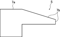
- FIG. 2 is a schematic diagram showing a half of the ring-shaped base material 5 cut away.
- the base material 5 has a film-forming surface 7 , and as shown in FIG. It may have two film-forming surfaces 7b.
- the ratio of the area of the second film forming surface 7b to the total area of the film forming surface 7 is, for example, 60% or less.
- FIG. 3 is a schematic diagram showing a part of a cross section of another ring-shaped base material 5. As shown in FIG. As shown in FIG. 3, the base material 5 may have a plurality of second film forming surfaces 7b.
- FIG. 4 is a schematic diagram showing a part of a cross section of yet another ring-shaped base material 5. As shown in FIG. The angle between the first film-forming surface 7a and the second film-forming surface 7b is, for example, 20° to 120°. In the base material 5 shown in FIG. 4, the angle between the first film-forming surface 7a and the second film-forming surface 7b connected to the first film-forming surface 7a is approximately 30°.
- one or more underlayers may be disposed between the base material and the yttrium protective film.
- the tensile stress of the yttrium-based protective film is relaxed to generate compressive stress, and the adhesion of the yttrium-based protective film to the base material is increased.
- the upper limit of the number of underlying layers is not particularly limited, but is preferably 5 or less, more preferably 4 or less, even more preferably 3 or less, particularly preferably 2 or less, and most preferably 1 layer.
- the base layer is preferably an amorphous film or a microcrystalline film.
- the base layer is made from the group consisting of Al 2 O 3 , SiO 2 , Y 2 O 3 , MgO, ZrO 2 , La 2 O 3 , Nd 2 O 3 , Yb 2 O 3 , Eu 2 O 3 and Gd 2 O 3 It is preferable to contain at least one selected oxide.
- the oxides of the underlayers are different between adjacent underlayers.
- the oxide of base layer 1 is " SiO2 "
- the oxide of base layer 2 is " Al2O3 +SiO2 "
- An example is a case where the oxide of the base layer 3 is "Al 2 O 3 ".
- each base layer is preferably 0.1 ⁇ m or more, more preferably 0.4 ⁇ m or more, and even more preferably 0.8 ⁇ m or more.
- the thickness of each base layer is, for example, 15 ⁇ m or less, preferably 10 ⁇ m or less, more preferably 7 ⁇ m or less, and even more preferably 3 ⁇ m or less.
- the thickness of the underlayer is measured in the same manner as the thickness of the yttrium protective film.
- This member is used, for example, as a member such as a top plate inside a semiconductor device manufacturing apparatus (plasma etching apparatus, plasma CVD apparatus, etc.). However, the use of this member is not limited to this.
- this manufacturing method is also a method for manufacturing the above-mentioned main member.
- This manufacturing method is a so-called ion-assisted deposition (IAD) method.
- IAD ion-assisted deposition
- an yttrium-based protective film containing Y 2 O 3 is formed by evaporating an evaporation source (Y 2 O 3 ) and attaching it to a base material while irradiating ions in a vacuum.
- the yttrium protective film can be formed very densely. That is, the obtained yttrium protective film has a low porosity. Also, the crystallite size is small.
- a dense and hard yttrium protective film can be obtained. Furthermore, when forming an underlayer, the tensile stress of the yttrium protective film is relaxed. Therefore, the yttrium protective film obtained by the present manufacturing method is difficult to crack even when the thickness is increased or the area is increased.
- the surface roughness (arithmetic mean roughness Ra) of the film-forming surface of the base material is preferably within the above-mentioned range.
- the formed yttrium-based protective film becomes denser and harder, and is less susceptible to cracks.
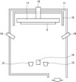
- FIG. 5 is a schematic diagram showing an apparatus used for manufacturing a yttrium-based protective film.
- the device shown in FIG. 5 has a chamber 11. The interior of the chamber 11 can be evacuated by driving and evacuating a vacuum pump (not shown).
- a crucible 12, a crucible 13, and an ion gun 14 are arranged inside the chamber 11, and a holder 17 is arranged above these.
- the holder 17 is integrated with the support shaft 16 and rotates as the support shaft 16 rotates.
- a heater 15 is arranged around the holder 17.
- the above-described base material 5 is held in the holder 17 with its film-forming surface facing downward.
- the base material 5 held by the holder 17 is heated by the heater 15 and rotates as the holder 17 rotates.
- a quartz crystal film thickness monitor 18 and a quartz crystal film thickness monitor 19 are attached to the chamber 11 .
- a yttrium protective film (not shown in FIG. 5) is formed on the base material 5 using the apparatus shown in FIG. First, one or both of crucible 12 and crucible 13 is filled with evaporation source Y 2 O 3 . After the base material 5 is held in the holder 17, the inside of the chamber 11 is evacuated to create a vacuum. Next, the holder 17 is rotated while the heater 15 is driven. Thereby, the base material 5 is rotated while being heated. In this state, ion-assisted vapor deposition is performed to form a film on the base material 5.
- the evaporation source Y 2 O 3 filled in one or both of the crucibles 12 and 13 is evaporated.
- the ions irradiated by the ion gun 14 are preferably ions of at least one element selected from the group consisting of oxygen, argon, neon, krypton, and xenon.
- the evaporation source is melted and evaporated by irradiating it with an electron beam (not shown). In this way, the evaporated evaporation source adheres to (the film-forming surface of) the base material 5, and an yttrium-based protective film is formed.
- the pressure inside the chamber 11 is preferably 6 ⁇ 10 ⁇ 2 Pa or less, more preferably 5 ⁇ 10 ⁇ 2 Pa or less, and 3 ⁇ 10 ⁇ 2 Pa or less. The following are more preferable.
- the pressure inside the chamber 11 is preferably more than 1 ⁇ 10 ⁇ 6 Pa, preferably 1 ⁇ 10 ⁇ 5 Pa or more, and more preferably 1 ⁇ 10 ⁇ 4 Pa or more.
- the temperature of the base material 5 heated by the heater 15 is preferably 200°C or higher, more preferably 250°C or higher. On the other hand, this temperature is preferably 400°C or lower, more preferably 350°C or lower.
- the rate at which the evaporation sources in the crucibles 12 and 13 evaporate to form a film is monitored using the crystal film thickness monitor 18 and the crystal film thickness monitor 19, respectively.
- the film formation rate is adjusted by controlling the conditions of the electron beam irradiated to the evaporation source and the conditions of the ion beam of the ion gun 14 (current value, current density, etc.).
- the deposition rate (unit: nm/min) of each evaporation source is adjusted to a desired value.
- the film formation rate of the evaporation source Y 2 O 3 is preferably 1 nm/min or more, more preferably 1.5 nm/min or more, and even more preferably 2 nm/min or more.
- the film formation rate of the evaporation source Y 2 O 3 is preferably 20 nm/min or less, more preferably 15 nm/min or less, and even more preferably 10 nm/min or less.
- the distance between the ion gun 14 and the base material 5 is preferably 700 mm or more, more preferably 900 mm or more. On the other hand, this distance is preferably 1500 mm or less, more preferably 1300 mm or less.
- the current value of the ion beam is preferably 1000 mA or more, more preferably 1500 mA or more. On the other hand, the ion beam current value is preferably 3000 mA or less, more preferably 2500 mA or less.
- the ion beam current density is preferably 40 ⁇ A/cm 2 or more, more preferably 65 ⁇ A/cm 2 or more, even more preferably 75 ⁇ A/cm 2 or more, and 77 ⁇ A/cm 2 because the obtained yttrium protective film becomes harder .
- the above is particularly preferable.
- the ion beam current density is preferably 140 ⁇ A/cm 2 or less, more preferably 120 ⁇ A/cm 2 or less, and even more preferably 100 ⁇ A/cm 2 or less.
- the yttrium protective film Before forming the yttrium protective film, it is preferable to form the above-mentioned base layer (for example, base layer 1, base layer 2, and base layer 3) on the film-forming surface of the base material 5.
- the base layer is formed by ion-assisted vapor deposition in the same way as the yttrium protective film.
- the base layer made of Al 2 O 3
- one or both of the crucibles 12 and 13 are filled with Al 2 O 3 as an evaporation source, and while irradiating ions (ion beam) from the ion gun 14, The evaporation source is evaporated and attached to the film-forming surface of the base material 5.
- the conditions for forming the base layer are similar to the conditions for forming the yttrium protective film.
- the base material may contain crystal water.
- crystals originating from hydrates which are low-temperature stable phases of aluminum oxide (e.g., boehmite ⁇ alumina)
- boehmite ⁇ alumina low-temperature stable phases of aluminum oxide
- the number of hydrogen atoms in the yttrium-based protective film tends to increase.
- a base layer is formed on the film-forming surface of the base material.
- the film-forming surface of the base material is covered, making it difficult for the crystal water of the base material to be included in the formed yttrium-based protective film, which in turn reduces the number of hydrogen atoms in the yttrium-based protective film. preferable.
- the evaporation source Y 2 O 3 is attached to the film-forming surface of the base material (in other words, the yttrium-based protective film
- the substrate is heated (pre-heated) at an elevated temperature before (forming) the substrate.
- the preheating temperature is preferably 300°C or higher, more preferably 400°C or higher, even more preferably 450°C or higher, and particularly preferably 500°C or higher.
- the preheating temperature is, for example, 800°C or lower, preferably 750°C or lower, and more preferably 700°C or lower.
- the preheating time is preferably 60 minutes or more, more preferably 120 minutes or more, even more preferably 240 minutes or more, and particularly preferably 480 minutes or more.
- the preheating time is preferably 1200 minutes or less, more preferably 1000 minutes or less, even more preferably 800 minutes or less, and particularly preferably 600° C. or less.
- the preheating atmosphere is, for example, an atmospheric atmosphere.
- Example 1 to 27, 30 to 31, and 39 to 42 are examples
- Examples 28 to 29, 32 to 33, and 37 to 38 are comparative examples
- Example 34 is a comparative example.
- Example 36 is a reference example.
- Example 1 A yttrium protective film (protective film) was manufactured using the apparatus described based on FIG. 5 under the conditions shown in Table 1 below.
- a circular base material made of aluminum oxide (Al 2 O 3 ) and having a film-forming surface with a diameter (maximum length) shown in Table 1 below was used.
- This base material was preheated in an air atmosphere while being held in a holder in a chamber.
- the preheating temperature was as shown in Table 1 below (unit: °C), and the preheating time was 600 minutes. If the base material was not preheated, a "-" was written in the preheating temperature column.
- a base layer and a yttrium protective film (protective film) shown in Table 1 below were formed on the film-forming surface of the base material.
- oxygen (O) ions were irradiated from an ion gun, the distance between the ion gun and the base material was 1100 mm, and the ion beam current value was 2000 mA.
- FIG. 6 is an XRD pattern of the yttrium-based protective film of Example 1. As shown in FIG. 6, it can be seen that in the yttrium protective film of Example 1, the (222) plane, which is the closest packed plane of the cubic crystal structure, is preferentially oriented around 28°.
- FIG. 7 is a SEM photograph of the surface of the yttrium-based protective film of Example 1.
- FIG. 8 is a cross-sectional SEM photograph of the yttrium protective film of Example 1. As shown in FIGS. 7 and 8, it can be seen that the yttrium protective film of Example 1 is very dense and has excellent smoothness. It can also be seen that the particle size is uniform.
- Example 2 to Example 33 In Examples 2 to 33, one or more conditions were changed from Example 1.
- a yttrium protective film (protective film) was produced in the same manner as in Example 1 except for the above.
- the outline is as follows. Note that in each example, there may be changes from Example 1 in addition to the description below.
- Example 2 the ion beam current density was changed from Example 1. In Examples 3 to 6, the number and/or composition of the underlying layer was changed from Example 1. In Examples 7 to 10, no underlayer was formed.
- Example 11 the base material and/or underlayer was changed from Example 1.
- Example 13 commercially available soda lime glass was used as the base material (glass).
- Example 15 one side of the base material made of aluminum single crystal was subjected to alumite treatment and then polished to form a base layer made of Al 2 O 3 . This base layer is described as "alumite” in Table 1 below.
- Example 16 one side of the aluminum base material was anodized using oxalic acid to form a base layer made of Al 2 O 3 . This base layer is described as "anodized layer” in Table 1 below.
- Example 21 and 22 the thickness of the protective film was changed from Example 1.
- Example 23 and 24 the area of the film forming surface was changed from Example 1.
- the chamber internal pressure was changed from Example 1.
- the protective film of Example 28 was amorphous (therefore, "-" was written in the "degree of orientation” column).
- the film formation rate was changed from Example 1.
- Example 32 and 33 the surface roughness (Ra) of the film-forming surface was changed from Example 1.
- Example 34 sapphire was used as the protective film.
- Example 35 metallic aluminum was used as the protective film.
- Example 36 quartz was used as the protective film.
- Example 37 the Y 2 O 3 protective film was formed using the IP method instead of the IAD method.
- Example 38 the Y 2 O 3 protective film was formed using the CVD method instead of the IAD method.
- Example 39 to Example 42 In Examples 39 to 42, protective films were formed in the same manner as in Example 7, Example 1, Example 3, and Example 26, respectively, except that the substrate was not preheated.
- test surface a part of the mirror-finished surface (referred to as "test surface") was masked by pasting Kapton tape.
- test surface a part of the mirror-finished surface
- plasma was generated by discharging in the gas described below, and a test in which the test surface was exposed to the generated plasma (exposure test). was carried out.
- discharge generation of plasma
- O 2 gas flow rate: 100 sccm
- F radicals are generated in the plasma. caused it to occur.
- a 15-minute discharge (plasma generation) was repeated five times, and an exposure test was conducted for a total of 150 minutes. In this way, the unmasked portion of the test surface was etched. Thereafter, the etching amount was determined by measuring the difference in level between the masked part and the non-masked part of the test surface using a stylus type surface profile measuring machine (manufactured by ULVAC, Dectak 150). The results are shown in Table 1 below. In addition, when ion etching or radical etching was not performed, "-" was written in Table 1 below.
- the etching amount (unit: nm) is, the better the plasma resistance is. Specifically, if the etching amount (ion etching amount, radical etching amount) is 200 nm or less, it can be evaluated that the plasma resistance is excellent.
- Example 2 By reducing the ion beam current density, the compressive stress of the protective film was reduced.
- Examples 8 to 10 As the surface roughness of the film-forming surface increased, the compressive stress of the protective film decreased.
- Example 12 Since the film formation rate was increased, the effect of ion irradiation was reduced and the compressive stress of the protective film was reduced.
- Example 13 This is an example in which soda lime glass was used as the base material, and the compressive stress of the protective film was reduced by lowering the temperature of the base material.
- Examples 26 to 27 Lowering the chamber pressure during film formation lengthens the mean free path and increases kinetic energy due to collisions between irradiated ions and particles (evaporation source), increasing compressive stress in the protective film. did.
- Example 28 Since the film formation rate was increased, the effect of ion irradiation was reduced and the compressive stress of the protective film was reduced.
- Example 29 By reducing the ion beam current density, the compressive stress of the protective film was reduced.
- Example 30 Since the temperature of the vapor deposition source was lowered, crystal growth was slowed down and the compressive stress of the protective film was reduced.
- Example 31 Because the pressure inside the chamber during film formation was lowered and the film formation rate was further lowered, the effect of ion irradiation became greater and the compressive stress of the protective film increased.
- Examples 32 to 33 Lowering the chamber pressure during film formation lengthens the mean free path and increases the kinetic energy due to collisions between irradiated ions and particles (evaporation source), increasing the compressive stress of the protective film. did.
- Examples 39 to 42 Since the substrate was not preheated, the number of hydrogen atoms in the protective film was increased compared to Example 7, Example 1, Example 3, and Example 26, in which the substrate was preheated, respectively.
- the specifications, claims, drawings, and abstracts of Japanese Patent Application No. 2022-131021 filed on August 19, 2022 and Japanese Patent Application No. 2022-175428 filed on November 1, 2022 The entire contents of this document are hereby incorporated by reference as a disclosure of the present invention.
- Base layer 4 Yttrium protective film 5: Base material 6: Member 7: Film forming surface 7a: First film forming surface 7b: Second film forming surface 11: Chambers 12, 13: Crucible 14: Ion gun 15: Heater 16: Support shaft 17: Holder 18, 19: Crystal film thickness monitor
Landscapes
- Chemical & Material Sciences (AREA)
- Engineering & Computer Science (AREA)
- Organic Chemistry (AREA)
- Chemical Kinetics & Catalysis (AREA)
- Materials Engineering (AREA)
- Metallurgy (AREA)
- Mechanical Engineering (AREA)
- Plasma & Fusion (AREA)
- Physics & Mathematics (AREA)
- General Chemical & Material Sciences (AREA)
- Health & Medical Sciences (AREA)
- Toxicology (AREA)
- Analytical Chemistry (AREA)
- Electrochemistry (AREA)
- Life Sciences & Earth Sciences (AREA)
- Geology (AREA)
- Inorganic Chemistry (AREA)
- Physical Vapour Deposition (AREA)
- Compounds Of Alkaline-Earth Elements, Aluminum Or Rare-Earth Metals (AREA)
Priority Applications (5)
| Application Number | Priority Date | Filing Date | Title |
|---|---|---|---|
| JP2024541433A JP7833151B2 (ja) | 2022-08-19 | 2023-06-21 | イットリウム質保護膜およびその製造方法ならびに部材 |
| CN202380060506.9A CN119731366A (zh) | 2022-08-19 | 2023-06-21 | 钇质保护膜和其制造方法以及部件 |
| KR1020257004562A KR20250053851A (ko) | 2022-08-19 | 2023-06-21 | 이트륨질 보호막 및 그의 제조 방법 그리고 부재 |
| US19/038,795 US20250171886A1 (en) | 2022-08-19 | 2025-01-28 | Yttrium-based protective film, method for producing same, and member |
| JP2026025142A JP2026069667A (ja) | 2022-08-19 | 2026-02-19 | イットリウム質保護膜およびその製造方法ならびに部材 |
Applications Claiming Priority (4)
| Application Number | Priority Date | Filing Date | Title |
|---|---|---|---|
| JP2022-131021 | 2022-08-19 | ||
| JP2022131021 | 2022-08-19 | ||
| JP2022-175428 | 2022-11-01 | ||
| JP2022175428 | 2022-11-01 |
Related Child Applications (1)
| Application Number | Title | Priority Date | Filing Date |
|---|---|---|---|
| US19/038,795 Continuation US20250171886A1 (en) | 2022-08-19 | 2025-01-28 | Yttrium-based protective film, method for producing same, and member |
Publications (1)
| Publication Number | Publication Date |
|---|---|
| WO2024038674A1 true WO2024038674A1 (ja) | 2024-02-22 |
Family
ID=89941449
Family Applications (1)
| Application Number | Title | Priority Date | Filing Date |
|---|---|---|---|
| PCT/JP2023/022986 Ceased WO2024038674A1 (ja) | 2022-08-19 | 2023-06-21 | イットリウム質保護膜およびその製造方法ならびに部材 |
Country Status (6)
| Country | Link |
|---|---|
| US (1) | US20250171886A1 (https=) |
| JP (2) | JP7833151B2 (https=) |
| KR (1) | KR20250053851A (https=) |
| CN (1) | CN119731366A (https=) |
| TW (1) | TW202409316A (https=) |
| WO (1) | WO2024038674A1 (https=) |
Cited By (3)
| Publication number | Priority date | Publication date | Assignee | Title |
|---|---|---|---|---|
| WO2025089226A1 (ja) * | 2023-10-26 | 2025-05-01 | Agc株式会社 | イットリウム質保護膜およびその製造方法ならびに部材 |
| WO2025089225A1 (ja) * | 2023-10-26 | 2025-05-01 | Agc株式会社 | イットリウム質保護膜およびその製造方法ならびに部材 |
| WO2025234334A1 (ja) * | 2024-05-08 | 2025-11-13 | Agc株式会社 | アルミナ焼結体、アルミナ焼結体の製造方法、部材およびプラズマ処理装置 |
Families Citing this family (1)
| Publication number | Priority date | Publication date | Assignee | Title |
|---|---|---|---|---|
| TWI863741B (zh) * | 2023-12-08 | 2024-11-21 | 翔名科技股份有限公司 | 靜電吸盤表面結構與其形成方法 |
Citations (7)
| Publication number | Priority date | Publication date | Assignee | Title |
|---|---|---|---|---|
| JP2001240482A (ja) * | 2000-02-29 | 2001-09-04 | Kyocera Corp | 耐プラズマ部材、高周波透過部材およびプラズマ装置 |
| JP2007131943A (ja) * | 2005-10-12 | 2007-05-31 | Toto Ltd | 複合構造物 |
| JP2007162099A (ja) * | 2005-12-15 | 2007-06-28 | Toyota Motor Corp | 硬質炭素膜及びその製造方法並びに摺動部材 |
| JP2008227190A (ja) * | 2007-03-13 | 2008-09-25 | Toto Ltd | 静電チャック、静電チャックの製造方法および基板処理装置 |
| JP2013136814A (ja) * | 2011-12-28 | 2013-07-11 | Fujimi Inc | セラミック溶射皮膜及びその製造方法 |
| US20180371634A1 (en) * | 2017-06-27 | 2018-12-27 | Dong Won KANG | Coating method for a plasma block and a plasma block coated by the same |
| WO2019044850A1 (ja) * | 2017-09-01 | 2019-03-07 | 学校法人 芝浦工業大学 | 部品および半導体製造装置 |
Family Cites Families (1)
| Publication number | Priority date | Publication date | Assignee | Title |
|---|---|---|---|---|
| JP6650385B2 (ja) | 2016-11-07 | 2020-02-19 | 東京エレクトロン株式会社 | 溶射用材料、溶射皮膜および溶射皮膜付部材 |
-
2023
- 2023-06-20 TW TW112123136A patent/TW202409316A/zh unknown
- 2023-06-21 KR KR1020257004562A patent/KR20250053851A/ko active Pending
- 2023-06-21 WO PCT/JP2023/022986 patent/WO2024038674A1/ja not_active Ceased
- 2023-06-21 JP JP2024541433A patent/JP7833151B2/ja active Active
- 2023-06-21 CN CN202380060506.9A patent/CN119731366A/zh active Pending
-
2025
- 2025-01-28 US US19/038,795 patent/US20250171886A1/en active Pending
-
2026
- 2026-02-19 JP JP2026025142A patent/JP2026069667A/ja active Pending
Patent Citations (7)
| Publication number | Priority date | Publication date | Assignee | Title |
|---|---|---|---|---|
| JP2001240482A (ja) * | 2000-02-29 | 2001-09-04 | Kyocera Corp | 耐プラズマ部材、高周波透過部材およびプラズマ装置 |
| JP2007131943A (ja) * | 2005-10-12 | 2007-05-31 | Toto Ltd | 複合構造物 |
| JP2007162099A (ja) * | 2005-12-15 | 2007-06-28 | Toyota Motor Corp | 硬質炭素膜及びその製造方法並びに摺動部材 |
| JP2008227190A (ja) * | 2007-03-13 | 2008-09-25 | Toto Ltd | 静電チャック、静電チャックの製造方法および基板処理装置 |
| JP2013136814A (ja) * | 2011-12-28 | 2013-07-11 | Fujimi Inc | セラミック溶射皮膜及びその製造方法 |
| US20180371634A1 (en) * | 2017-06-27 | 2018-12-27 | Dong Won KANG | Coating method for a plasma block and a plasma block coated by the same |
| WO2019044850A1 (ja) * | 2017-09-01 | 2019-03-07 | 学校法人 芝浦工業大学 | 部品および半導体製造装置 |
Non-Patent Citations (1)
| Title |
|---|
| KIYOHARA MASAKATSU, HIRONORI HATONO, JUNICHI IWASAWA: "A New Plasma Resistant Coating Reducing Particle Generations", JOURNAL OF THE VACUUM SOCIETY OF JAPAN, vol. 53, no. 10, 1 January 2010 (2010-01-01), pages 573 - 577, XP093140027 * |
Cited By (3)
| Publication number | Priority date | Publication date | Assignee | Title |
|---|---|---|---|---|
| WO2025089226A1 (ja) * | 2023-10-26 | 2025-05-01 | Agc株式会社 | イットリウム質保護膜およびその製造方法ならびに部材 |
| WO2025089225A1 (ja) * | 2023-10-26 | 2025-05-01 | Agc株式会社 | イットリウム質保護膜およびその製造方法ならびに部材 |
| WO2025234334A1 (ja) * | 2024-05-08 | 2025-11-13 | Agc株式会社 | アルミナ焼結体、アルミナ焼結体の製造方法、部材およびプラズマ処理装置 |
Also Published As
| Publication number | Publication date |
|---|---|
| JP2026069667A (ja) | 2026-04-23 |
| TW202409316A (zh) | 2024-03-01 |
| JPWO2024038674A1 (https=) | 2024-02-22 |
| CN119731366A (zh) | 2025-03-28 |
| KR20250053851A (ko) | 2025-04-22 |
| JP7833151B2 (ja) | 2026-03-19 |
| US20250171886A1 (en) | 2025-05-29 |
Similar Documents
| Publication | Publication Date | Title |
|---|---|---|
| WO2024038674A1 (ja) | イットリウム質保護膜およびその製造方法ならびに部材 | |
| JP7154517B1 (ja) | イットリウム質保護膜およびその製造方法ならびに部材 | |
| US20110135915A1 (en) | Methods of Coating Substrate With Plasma Resistant Coatings and Related Coated Substrates | |
| TWI889861B (zh) | 基於氧化釔之塗層及塊體組成物 | |
| JP6388188B1 (ja) | 成膜用材料及び皮膜 | |
| US6524731B1 (en) | Corrosion-resistant member and method of producing the same | |
| JP2005097685A (ja) | 耐食性部材およびその製造方法 | |
| JP5031259B2 (ja) | 耐食性部材とその製造方法およびこれを用いた半導体・液晶製造装置 | |
| US20250290191A1 (en) | Member and method for producing same | |
| TWI778587B (zh) | 複合結構物及具備複合結構物之半導體製造裝置 | |
| US20250270685A1 (en) | Yttrium-based protective film, method for producing same, and member | |
| TW202517585A (zh) | 釔質保護膜及其製造方法以及構件 | |
| TW201334035A (zh) | 抗電漿蝕刻膜,承載抗電漿蝕刻膜之物品及相關的方法 | |
| TW202534181A (zh) | 釔質保護膜及其製造方法以及構件 | |
| WO2025177799A1 (ja) | イットリウム質保護膜、部材およびその製造方法 | |
| TWI777504B (zh) | 複合結構物及具備複合結構物之半導體製造裝置 | |
| WO2024225362A1 (ja) | 酸化アルミニウム質膜およびその製造方法ならびに積層体 | |
| TW202346240A (zh) | 複合結構物及具備複合結構物之半導體製造裝置 | |
| TW202238998A (zh) | 複合結構物及具備複合結構物之半導體製造裝置 | |
| WO2023162743A1 (ja) | 複合構造物および複合構造物を備えた半導体製造装置 | |
| TW202237397A (zh) | 複合結構物及具備複合結構物之半導體製造裝置 | |
| HK40125970A (zh) | 晶圆支承体 | |
| JP2022153274A (ja) | 複合構造物および複合構造物を備えた半導体製造装置 |
Legal Events
| Date | Code | Title | Description |
|---|---|---|---|
| 121 | Ep: the epo has been informed by wipo that ep was designated in this application |
Ref document number: 23854712 Country of ref document: EP Kind code of ref document: A1 |
|
| WWE | Wipo information: entry into national phase |
Ref document number: 2024541433 Country of ref document: JP |
|
| WWE | Wipo information: entry into national phase |
Ref document number: 202380060506.9 Country of ref document: CN |
|
| NENP | Non-entry into the national phase |
Ref country code: DE |
|
| WWP | Wipo information: published in national office |
Ref document number: 202380060506.9 Country of ref document: CN |
|
| WWP | Wipo information: published in national office |
Ref document number: 1020257004562 Country of ref document: KR |
|
| 122 | Ep: pct application non-entry in european phase |
Ref document number: 23854712 Country of ref document: EP Kind code of ref document: A1 |