WO2024038650A1 - 積層セラミックコンデンサ - Google Patents
積層セラミックコンデンサ Download PDFInfo
- Publication number
- WO2024038650A1 WO2024038650A1 PCT/JP2023/019394 JP2023019394W WO2024038650A1 WO 2024038650 A1 WO2024038650 A1 WO 2024038650A1 JP 2023019394 W JP2023019394 W JP 2023019394W WO 2024038650 A1 WO2024038650 A1 WO 2024038650A1
- Authority
- WO
- WIPO (PCT)
- Prior art keywords
- layer
- ceramic capacitor
- multilayer ceramic
- electrode layer
- internal electrode
- Prior art date
Links
- 239000003985 ceramic capacitor Substances 0.000 title claims abstract description 55
- 238000003475 lamination Methods 0.000 claims abstract description 8
- 229910000679 solder Inorganic materials 0.000 claims description 15
- 239000003990 capacitor Substances 0.000 abstract description 2
- 230000002093 peripheral effect Effects 0.000 abstract description 2
- 238000007747 plating Methods 0.000 description 43
- 229910052751 metal Inorganic materials 0.000 description 8
- 239000003989 dielectric material Substances 0.000 description 7
- 239000002184 metal Substances 0.000 description 7
- 150000001875 compounds Chemical class 0.000 description 6
- 239000000919 ceramic Substances 0.000 description 5
- 229910010293 ceramic material Inorganic materials 0.000 description 5
- 239000010409 thin film Substances 0.000 description 5
- 239000011521 glass Substances 0.000 description 4
- 229910001252 Pd alloy Inorganic materials 0.000 description 3
- 229910052802 copper Inorganic materials 0.000 description 3
- 230000000694 effects Effects 0.000 description 3
- 239000000463 material Substances 0.000 description 3
- 150000002739 metals Chemical class 0.000 description 3
- 229910052759 nickel Inorganic materials 0.000 description 3
- 229910052763 palladium Inorganic materials 0.000 description 3
- 229910052709 silver Inorganic materials 0.000 description 3
- 229910002367 SrTiO Inorganic materials 0.000 description 2
- 230000015572 biosynthetic process Effects 0.000 description 2
- 238000012790 confirmation Methods 0.000 description 2
- 238000010586 diagram Methods 0.000 description 2
- 238000010304 firing Methods 0.000 description 2
- 238000000034 method Methods 0.000 description 2
- 229920005989 resin Polymers 0.000 description 2
- 239000011347 resin Substances 0.000 description 2
- 229920003002 synthetic resin Polymers 0.000 description 2
- 239000000057 synthetic resin Substances 0.000 description 2
- 238000009736 wetting Methods 0.000 description 2
- 239000000956 alloy Substances 0.000 description 1
- JRPBQTZRNDNNOP-UHFFFAOYSA-N barium titanate Chemical compound [Ba+2].[Ba+2].[O-][Ti]([O-])([O-])[O-] JRPBQTZRNDNNOP-UHFFFAOYSA-N 0.000 description 1
- 229910002113 barium titanate Inorganic materials 0.000 description 1
- 239000011230 binding agent Substances 0.000 description 1
- 230000000052 comparative effect Effects 0.000 description 1
- 239000004020 conductor Substances 0.000 description 1
- 239000000470 constituent Substances 0.000 description 1
- 230000008602 contraction Effects 0.000 description 1
- 239000002270 dispersing agent Substances 0.000 description 1
- 239000003822 epoxy resin Substances 0.000 description 1
- LNEPOXFFQSENCJ-UHFFFAOYSA-N haloperidol Chemical compound C1CC(O)(C=2C=CC(Cl)=CC=2)CCN1CCCC(=O)C1=CC=C(F)C=C1 LNEPOXFFQSENCJ-UHFFFAOYSA-N 0.000 description 1
- 239000012212 insulator Substances 0.000 description 1
- 229910001092 metal group alloy Inorganic materials 0.000 description 1
- 239000002923 metal particle Substances 0.000 description 1
- 239000003960 organic solvent Substances 0.000 description 1
- 239000005011 phenolic resin Substances 0.000 description 1
- 229920006122 polyamide resin Polymers 0.000 description 1
- 229920000647 polyepoxide Polymers 0.000 description 1
- 229920013716 polyethylene resin Polymers 0.000 description 1
- 229920001721 polyimide Polymers 0.000 description 1
- 239000009719 polyimide resin Substances 0.000 description 1
- 239000000843 powder Substances 0.000 description 1
- 238000005245 sintering Methods 0.000 description 1
- 238000004544 sputter deposition Methods 0.000 description 1
- 239000000758 substrate Substances 0.000 description 1
- 229920005992 thermoplastic resin Polymers 0.000 description 1
- 229920001187 thermosetting polymer Polymers 0.000 description 1
- 229910052718 tin Inorganic materials 0.000 description 1
- 238000007740 vapor deposition Methods 0.000 description 1
Images


Classifications
-
- H—ELECTRICITY
- H01—ELECTRIC ELEMENTS
- H01G—CAPACITORS; CAPACITORS, RECTIFIERS, DETECTORS, SWITCHING DEVICES OR LIGHT-SENSITIVE DEVICES, OF THE ELECTROLYTIC TYPE
- H01G4/00—Fixed capacitors; Processes of their manufacture
- H01G4/30—Stacked capacitors
Definitions
- the present invention relates to a multilayer ceramic capacitor that can suppress the generation of vibration noise caused by piezoelectric phenomena during mounting.
- a multilayer ceramic capacitor is composed of a rectangular parallelepiped-shaped laminate in which dielectric layers and internal electrode layers are alternately laminated, and external electrodes formed at opposing ends of the laminate.
- the dielectric that constitutes the dielectric layer is usually a dielectric ceramic with a perovskite structure such as barium titanate, so if an alternating current voltage is applied while a direct current voltage is applied, vibrations occur due to piezoelectric phenomena. Therefore, when a multilayer ceramic capacitor is mounted on a wiring board and, for example, an AC voltage in the audible frequency band of 20Hz to 20kHz is applied to the external electrode, the multilayer ceramic capacitor expands and contracts and vibrates, causing the surrounding air to vibrate and produce sound. When this occurs, the wiring board also vibrates resonantly, causing the problem that the sound is amplified and becomes harsh.
- An object of the present invention is to provide a multilayer ceramic capacitor that can suppress vibrations of a dielectric material caused by piezoelectric phenomena that occur when mounted on a wiring board, and can reduce harsh vibration noise.
- the present inventor discovered that by arranging an insulator at a predetermined position of the external electrode of a multilayer ceramic capacitor, it is possible to suppress the vibration noise caused by the piezoelectric phenomenon that occurs when the capacitor is mounted, and was able to complete the present invention. Ta.
- the present invention provides a laminate in which dielectric layers and internal electrode layers are alternately laminated, and a laminate in which dielectric layers and internal electrode layers are arranged on both end faces of the laminate in a longitudinal direction perpendicular to the lamination direction and connected to the internal electrode layers.
- a multilayer ceramic capacitor having an external electrode The external electrode is a multilayer ceramic capacitor whose surface, when viewed in plan from the longitudinal direction, is covered with an insulating layer except for a frame region having a width of 1 ⁇ m or more and 100 ⁇ m or less from the outer periphery.
- the present invention it is possible to provide a multilayer ceramic capacitor that can suppress vibrations of a dielectric material caused by piezoelectric phenomena that occur when mounted on a wiring board, and can reduce unpleasant vibration noise.
- FIG. 2 is an external view of a multilayer ceramic capacitor. 2 is a cross-sectional view taken along line AA of the multilayer ceramic capacitor shown in FIG. 1.
- FIG. FIG. 3 is an exploded perspective view schematically showing an example of an inner layer part. 1 is an external view showing an example of a mounting state of a multilayer ceramic capacitor according to the present invention.
- FIG. 2 is an external view showing an example of a mounting state of a conventional multilayer ceramic capacitor.
- FIG. 3 is a diagram showing the effect of reducing vibration noise of the multilayer ceramic capacitor according to the present invention.
- FIG. 1 is an external view of a multilayer ceramic capacitor 1.
- FIG. 2 is a cross-sectional view (LT cross-sectional view) of the multilayer ceramic capacitor 1 taken along the line AA at the center in the width direction W shown in FIG.
- FIG. 3 is a schematic diagram showing the structure of the inner layer portion 3.
- the direction in which the dielectric layers and internal electrode layers are laminated is defined as the lamination direction T
- the length direction L is perpendicular to the lamination direction T
- the width direction W is perpendicular to the lamination direction T and the length direction L.
- the structure of the ceramic capacitor 1 will be described.
- the width direction W, the length direction L, and the lamination direction T are orthogonal to each other, but they are not necessarily orthogonal to each other, and may be intersecting to each other.
- the multilayer ceramic capacitor 1 includes a multilayer body 2 having a rectangular parallelepiped shape.
- the laminate 2 includes an inner layer part 3, and has a pair of first main surfaces TS1 and second main surfaces TS2 facing each other in the stacking direction T, and a pair of first main surfaces TS1 and second main surfaces TS2 facing each other in the length direction L perpendicular to the stacking direction T. It has a pair of first end surfaces LS1 and a second end surface LS2, and a pair of first side surfaces WS1 and second side surfaces WS2 that face each other in the width direction W perpendicular to both the stacking direction T and the length direction L. ing.
- the dimensions of the multilayer ceramic capacitor 1 are not particularly limited, but for example, the dimensions in the stacking direction T are about 0.1 mm to 2.5 mm, and the dimensions in the length direction L are about 0.1 mm to 3.2 mm.
- the dimension in the width direction W can be approximately 0.1 mm to 2.5 mm.
- the inner layer portion 3 is composed of a plurality of dielectric layers 5 and a plurality of internal electrode layers 6 stacked together.
- the internal electrode layer 6 is composed of a first internal electrode layer 6a and a second internal electrode layer 6b.
- the first internal electrode layer 6a and the second internal electrode layer 6b are arranged on the dielectric layers 5a and 5b, respectively.
- the internal electrode layer 6 extends in the length direction L and has a rectangular shape when viewed in plan from the stacking direction T.
- the first internal electrode layer 6a is drawn out to the first end surface LS1 of the laminate 2
- the second internal electrode layer 6b is drawn out to the second end surface LS2 of the laminate 2.
- the dielectric layer 5 is made of a dielectric material.
- a dielectric ceramic containing components such as BaTiO 3 , CaTiO 3 , SrTiO 3 , or CaZrO 3 can be used.
- the dielectric material may be one in which subcomponents such as Mn compounds, Fe compounds, Cr compounds, Co compounds, and Ni compounds are added to these main components.
- the thickness of the dielectric layer 5 is not particularly limited, but is, for example, 0.3 ⁇ m to 2.0 ⁇ m in the effective region of capacitance formation formed by the first internal electrode layer 6a and the second internal electrode layer 6b. It can be about 0 ⁇ m.
- the number of layers of the dielectric layer 5 is not particularly limited, but for example, in the effective area of capacitance formation formed by the first internal electrode layer 6a and the second internal electrode layer 6b, the number of layers is 1 to 6000 layers. It can be done.
- an outer layer portion 7 is provided, which is composed only of the dielectric layer 5 without the internal electrode layer 6 formed thereon.
- the thickness of the outer layer portion 7 is not limited, but may be, for example, 15 ⁇ m to 150 ⁇ m. Note that the thickness of the dielectric layer in the outer layer portion 7 may be larger than the thickness of the dielectric layer in the effective area for forming capacitance where the internal electrode layer 6 is formed. Further, the material of the dielectric layer in the outer layer portion may be different from the material of the dielectric layer in the inner layer portion.
- FIG. 3 shows the inner layer portion 3 broken down into dielectric layers 5 in the stacking direction T.
- the internal electrode layer 6 is formed by sintering a conductive paste containing a metal powder serving as a conductor, an organic solvent, a binder, and a dispersant on the dielectric layer.
- the internal electrode layers 6 and the dielectric layers 5 are alternately laminated to form the inner layer portion 3.
- the internal electrode layer 6 is composed of a first internal electrode layer 6a and a second internal electrode layer 6b, and the first internal electrode layer 6a and the second internal electrode layer 6b are arranged on the dielectric layers 5a and 5b, respectively. ing.
- metals such as Ni, Cu, Ag, Pd, Ag-Pd alloy, and Au can be used. Further, these metals may be compounds containing these metal elements or alloys with other metals.
- the thickness of the internal electrode layer 6 is not particularly limited, but may be, for example, about 0.3 ⁇ m to 1.5 ⁇ m.
- a first external electrode 4a and a second external electrode 4b are formed on the first end surface LS1 and the second end surface LS2 of the laminate 2, respectively.
- the first external electrode 4a includes a first base electrode layer 41a and a first plating layer 42a disposed on the first base electrode layer 41a.
- the second external electrode 4b includes a second base electrode layer 41b and a second plating layer 42b disposed on the second base electrode layer 41b.
- the first base electrode layer 41a is arranged on the first end surface LS1.
- the first base electrode layer 41a is connected to the first internal electrode layer 6a.
- the first base electrode layer 41a extends from above the first end surface LS1 to a part of the first main surface TS1 and a part of the second main surface TS2, and a part of the first side surface WS1 and the second side surface. It is formed to extend to a part of WS2.
- the second base electrode layer 41b is arranged on the second end surface LS2.
- the second base electrode layer 41b is connected to the second internal electrode layer 6b.
- the second base electrode layer 41b extends from above the second end surface LS2 to a part of the first main surface TS1 and a part of the second main surface TS2, and a part of the first side surface WS1 and the second side surface. It is formed to extend to a part of WS2.
- the first base electrode layer 41a and the second base electrode layer 41b include at least one selected from a baked layer, a conductive resin layer, a thin film layer, and the like.
- the first base electrode layer 41a and the second base electrode layer 41b of this embodiment are baked layers.
- the baking layer contains a metal component and either a glass component or a ceramic component, or both.
- the metal component includes, for example, at least one selected from Cu, Ni, Ag, Pd, Ag-Pd alloy, Au, and the like.
- the glass component includes, for example, at least one selected from B, Si, Ba, Mg, Al, Li, and the like.
- the ceramic component the same type of ceramic material as the dielectric layer 5 may be used, or a different type of ceramic material may be used.
- the ceramic component includes, for example, at least one selected from BaTiO 3 , CaTiO 3 , (Ba,Ca)TiO 3 , SrTiO 3 , CaZrO 3 , and the like.
- the baked layer is, for example, a layered product coated with a conductive paste containing glass and metal and baked.
- the baked layer may be obtained by simultaneously firing a multilayer chip having an internal electrode layer and a dielectric layer and a conductive paste applied to the multilayer chip, or by baking a multilayer chip having an internal electrode layer and a dielectric layer to create a multilayer product. After obtaining the laminate, a conductive paste may be applied to the laminate and baked.
- the baked layer is formed by baking a ceramic material added instead of a glass component. It is preferable to do so. In this case, it is particularly preferable to use the same type of ceramic material as the dielectric layer as the added ceramic material.
- the baking layer may have multiple layers.
- the thickness in the length direction L of the first base electrode layer 41a located on the first end surface LS1 is, for example, about 3 ⁇ m or more and 160 ⁇ m or less at the center of the first base electrode layer 41a in the stacking direction T and width direction W. It is preferable.
- the thickness in the length direction L of the second base electrode layer 41b located on the second end surface LS2 is, for example, about 3 ⁇ m or more and 160 ⁇ m or less at the center of the second base electrode layer 41b in the stacking direction T and width direction W. It is preferable.
- the stacking direction T of the first base electrode layer 41a provided on this part is The thickness of the first base electrode layer 41a provided in this portion is preferably about 3 ⁇ m or more and 40 ⁇ m or less at the central portion in the length direction L and width direction W, for example.
- the thickness in the width direction W of the first base electrode layer 41a provided on this part is preferably, for example, approximately 3 ⁇ m or more and 40 ⁇ m or less in the center portion of the first base electrode layer 41a provided in this portion in the length direction L and the stacking direction T.
- the stacking direction T of the second base electrode layer 41b provided on this part is preferably about 3 ⁇ m or more and 40 ⁇ m or less at the central portion in the length direction L and width direction W, for example.
- the thickness in the width direction W of the second base electrode layer 41b provided on this part is preferably, for example, approximately 3 ⁇ m or more and 40 ⁇ m or less in the central portion of the second base electrode layer 41b provided in this portion in the length direction L and the stacking direction T.
- a configuration may be adopted in which a first plating layer 42a and a second plating layer 42b, which will be described later, are directly arranged on the laminate 2 without providing the first base electrode layer 41a and the second base electrode layer 41b.
- the first base electrode layer 41a and the second base electrode layer 41b are not limited to baked layers, but may be thin film layers.
- the thin film layer is formed by a thin film forming method such as a sputtering method or a vapor deposition method.
- the thin film layer is a layer of 1 ⁇ m or less on which metal particles are deposited.
- the first plating layer 42a is arranged to cover the first base electrode layer 41a.
- the second plating layer 42b is arranged to cover the second base electrode layer 41b.
- the first plating layer 42a and the second plating layer 42b may contain, for example, at least one selected from Cu, Ni, Sn, Ag, Pd, Ag-Pd alloy, Au, and the like.
- the first plating layer 42a and the second plating layer 42b may each be formed of multiple layers.
- the first plating layer 42a and the second plating layer 42b preferably have a two-layer structure in which Sn plating layers 422a and 422b are formed on Ni plating layers 421a and 421b, respectively.
- the Ni plating layers 421a and 421b prevent the first base electrode layer 41a and the second base electrode layer 41b from being eroded by solder when mounting the multilayer ceramic capacitor 1.
- the Sn plating layer improves solder wettability when mounting the multilayer ceramic capacitor 1. This facilitates mounting of the multilayer ceramic capacitor 1.
- the thickness of each of the Ni plating layer and the Sn plating layer should be 2 ⁇ m or more and 15 ⁇ m or less. preferable.
- the surfaces of the first external electrode 4a and the second external electrode 4b when viewed in plan from the length direction L are covered with an insulating layer 8 except for a frame region 9 having a width of 1 ⁇ m or more and 100 ⁇ m or less from the outer periphery.
- the insulating layer can be placed in a predetermined range on the surface of the plating layer.
- the plating layer is formed on the surface of the base electrode layer except for the area where the insulating layer is disposed.
- an insulating layer can be placed in a predetermined range on the surface of the outermost plating layer, but an insulating layer can be placed on the surface of any plating layer other than the outermost layer.
- the plating layer should be stacked on the part excluding the area where the insulating layer is placed, and the plating layer should be placed on the part where the insulating layer is placed, and the plating layer should be placed on the part where the insulating layer is placed, and the plating layer should be stacked on the part of the plating layer that is placed on the plating layer where the insulating layer is placed.
- the structure is such that an insulating layer is disposed on the surface.
- An insulating layer 8 is formed on the surface of the outer peripheral edge excluding a frame region 9 having a width of 1 ⁇ m or more and 100 ⁇ m or less, and a first base electrode layer 41a and a second base electrode layer excluding the area where the insulating layer 8 is disposed.
- Ni plating layers 421a, 421b and Sn plating layers 422a, 422b are formed on the surface of 41b.
- the multilayer ceramic capacitor 1 is connected to lands 51a and 51b by applying solder to the surfaces of the first external electrode 4a and the second external electrode 4b below the insulating layer 8.
- solder By providing the frame region 9, a solder fillet can be formed within a certain height range from below the outer periphery, so that bonding to the wiring board can be performed reliably.
- the material of the insulating layer 8 is not particularly limited as long as it has insulating properties, but it is preferable to use a synthetic resin because the insulating layer can be easily formed on the surface of the external electrode.
- a synthetic resin thermosetting resins such as epoxy resins, polyimide resins, and phenol resins, and thermoplastic resins such as polyethylene resins and polyamide resins can be used.
- the internal It is possible to prevent the solder fillets 52a and 52b from getting wet up to the height at which the electrode layer 6 is arranged. Thereby, generation of vibration noise caused by piezoelectric phenomenon can be effectively suppressed.
- the insulating layer 8 has a thickness in the length direction L of 200 ⁇ m or less, and is thickest at approximately the center when viewed from the length direction L. This prevents the multilayer ceramic capacitor from increasing in size, and when it is mounted on a wiring board, the center part of the surface of the insulating layer protrudes outward from the bottom part, which reduces wetting of the solder fillet. This makes it possible to reliably prevent this.
- the multilayer ceramic capacitor 1 is mounted by applying solder to the surfaces of the first external electrode 4a and the second external electrode 4b and connecting them to the lands 51a and 51b. As shown, when the wetting height of the solder fillets 52a and 52b formed during mounting is high and reaches the height at which the internal electrode layer 6 is arranged, a piezoelectric phenomenon of the dielectric occurs, and the expansion and contraction vibration of the multilayer ceramic capacitor 1 occurs. is likely to occur.
- FIG. 4 shows a mounting example of the multilayer ceramic capacitor 1 according to this embodiment.
- the insulating layer 8 is provided in a predetermined range on the surfaces of the first external electrode 4a and the second external electrode 4b, the height at which the solder fillets 52a and 52b are wetted is suppressed to a low level, and the piezoelectric phenomenon is suppressed. The generation of vibration noise caused by this can be suppressed.
- the multilayer ceramic capacitor (example) of the present invention it is possible to suppress the vibration of the dielectric material caused by the piezoelectric phenomenon that occurs when it is mounted on a wiring board, and to reduce the harsh vibration noise. I was able to confirm.
- the present invention is not limited to the embodiments, and can be implemented in various forms without departing from the gist of the present invention.
- the embodiment has shown an example in which the insulating layer 8 is provided on both the first external electrode 4a and the second external electrode 4b, the insulating layer 8 is provided on either the first external electrode 4a or the second external electrode 4b. Similar effects can be expected to be obtained when
- the present invention is as follows.
- ⁇ 1> A laminate in which dielectric layers and internal electrode layers are alternately laminated; and external electrodes arranged on both end faces of the laminate in a longitudinal direction perpendicular to the lamination direction and connected to the internal electrode layers.
- a multilayer ceramic capacitor having In the multilayer ceramic capacitor, the surface of the external electrode when viewed in plan from the length direction is covered with an insulating layer except for a frame region having a width of 1 ⁇ m or more and 100 ⁇ m or less from the outer periphery.
- ⁇ 2> The multilayer ceramic capacitor according to ⁇ 1>, wherein a surface of the external electrode corresponding to a region where the internal electrode layer is laminated when viewed in plan from the length direction is covered with the insulating layer.
- ⁇ 3> The multilayer ceramic capacitor according to ⁇ 1> or ⁇ 2>, wherein the insulating layer has a thickness of 200 ⁇ m or less in the length direction, and is thickest at approximately the center when viewed from the length direction.
- a mounting comprising the multilayer ceramic capacitor according to any one of ⁇ 1> to ⁇ 3>, a land arranged on a wiring board, and a solder connecting the external electrode and the land of the multilayer ceramic capacitor.
- Multilayer ceramic capacitor 2 Laminated body 3 Inner layer portion 4 External electrode 4a First external electrode 4b Second external electrode 5 Dielectric layer 5a Dielectric layer 5b Dielectric layer 6 Internal electrode layer 6a First internal electrode layer 6b Second internal electrode Layer 7 Outer layer 8 Insulating layer 9 Frame region 41a First base electrode layer 41b Second base electrode layer 42a First plating layer 42b Second plating layer 421a Ni plating layer 421b Ni plating layer 422a Sn plating layer 422b Sn plating layer 50 Wiring Substrate 51a Land 51b Land 52a Solder fillet 52b Solder fillet TS1 First main surface TS2 Second main surface WS1 First side surface WS2 Second side surface LS1 First end surface LS2 Second end surface
Abstract
配線基板に実装した際に生じる圧電現象を起因とする誘電体の振動を抑え、耳障りな振動音を低減することができる積層セラミックコンデンサを提供すること。 誘電体層5と内部電極層6とが交互に積層された積層体2と、前記積層体2の積層方向Tと直交する長さ方向Lの両側の端面にそれぞれ配置され且つ前記内部電極層6と接続された外部電極4と、を有する積層セラミックコンデンサであって、前記外部電極4は、前記長さ方向Lから平面視したときの表面を、外周縁から幅1μm以上100μm以下の枠領域9を除き、絶縁層8で覆われている、積層セラミックコンデンサ1。
Description
本発明は、実装時における圧電現象を起因とする振動音の発生を抑制することができる積層セラミックコンデンサに関する。
従来より、積層セラミックコンデンサなどの電子部品は、携帯電話機等の移動体端末機器又はパーソナルコンピューターなどの各種電子機器に多く利用されている。積層セラミックコンデンサは、誘電体層と内部電極層とを交互に積層した直方体状の積層体と、当該積層体の対向する両端に形成された外部電極とから構成される。
誘電体層を構成する誘電体は、通常、チタン酸バリウムなどのペロブスカイト型構造の誘電体セラミックを用いることから、直流電圧を印加しながら、交流電圧を印加すると圧電現象により振動が発生する。そのため、積層セラミックコンデンサが配線基板に実装され、例えば、20Hz~20kHzの可聴周波数帯域の交流電圧が外部電極に印加されると、積層セラミックコンデンサが伸縮振動し、周囲の空気が振動して音が発生すると共に、配線基板も共鳴振動し、音が増幅され耳障りになるという問題があった。
このため、配線基板に実装した際に生じる圧電現象を起因とする誘電体の振動を抑え、耳障りな振動音を低減することができる積層セラミックコンデンサの開発が求められる。
本発明は、配線基板に実装した際に生じる圧電現象を起因とする誘電体の振動を抑え、耳障りな振動音を低減することができる積層セラミックコンデンサを提供することを目的とする。
本発明者は、積層セラミックコンデンサの外部電極の所定の位置に絶縁体を配置することにより、実装した際に生じる圧電現象を起因とする振動音を抑制できることを見出し、本発明を完成するに至った。
すなわち本発明は、誘電体層と内部電極層とが交互に積層された積層体と、前記積層体の積層方向と直交する長さ方向の両側の端面にそれぞれ配置され且つ前記内部電極層と接続された外部電極と、を有する積層セラミックコンデンサであって、
前記外部電極は、前記長さ方向から平面視したときの表面を、外周縁から幅1μm以上100μm以下の枠領域を除き、絶縁層で覆われている、積層セラミックコンデンサである。
前記外部電極は、前記長さ方向から平面視したときの表面を、外周縁から幅1μm以上100μm以下の枠領域を除き、絶縁層で覆われている、積層セラミックコンデンサである。
本発明によれば、配線基板に実装した際に生じる圧電現象を起因とする誘電体の振動を抑え、耳障りな振動音を低減することができる積層セラミックコンデンサを提供することが可能となる。
以下、本発明の実施形態の積層セラミックコンデンサについて説明するが、本発明がこれに限定されることはない。また、図面は、発明の内容を説明するため、模式的に簡略化して描画している場合があり、描画された構成要素又は構成要素間の寸法の比率が、明細書に記載されたそれらの寸法の比率と一致していない場合がある。また、明細書に記載されている構成要素が、図面において省略されている場合や、個数を省略して描画されている場合などがある。
(積層セラミックコンデンサ)
図1~図3に、積層セラミックコンデンサ1の形状及び構造を示す。図1は、積層セラミックコンデンサ1の外観図である。図2は、図1に示す幅方向W中央部のA-A線で切断した積層セラミックコンデンサ1の断面図(LT断面図)である。図3は、内層部3の構造を示す模式図である。なお、誘電体層と内部電極層を積層する方向を積層方向Tとし、積層方向Tに直交する長さ方向L、さらに積層方向Tと長さ方向Lに直交する幅方向Wを用いて、積層セラミックコンデンサ1の構造について言及する。なお、実施形態においては、幅方向W、長さ方向L、及び積層方向Tは、互いに直交しているが、必ずしも互いに直交する関係になるとは限らず、互いに交差する関係であってもよい。
図1~図3に、積層セラミックコンデンサ1の形状及び構造を示す。図1は、積層セラミックコンデンサ1の外観図である。図2は、図1に示す幅方向W中央部のA-A線で切断した積層セラミックコンデンサ1の断面図(LT断面図)である。図3は、内層部3の構造を示す模式図である。なお、誘電体層と内部電極層を積層する方向を積層方向Tとし、積層方向Tに直交する長さ方向L、さらに積層方向Tと長さ方向Lに直交する幅方向Wを用いて、積層セラミックコンデンサ1の構造について言及する。なお、実施形態においては、幅方向W、長さ方向L、及び積層方向Tは、互いに直交しているが、必ずしも互いに直交する関係になるとは限らず、互いに交差する関係であってもよい。
積層セラミックコンデンサ1は、直方体形状からなる積層体2を備えている。積層体2は、内層部3を含み、積層方向Tにおいて相互に対向する1対の第1主面TS1、第2主面TS2と、積層方向Tに直交する長さ方向Lにおいて相互に対向する1対の第1端面LS1、第2端面LS2と、積層方向T及び長さ方向Lの両方に直交する幅方向Wにおいて相互に対向する1対の第1側面WS1、第2側面WS2を有している。
積層セラミックコンデンサ1の寸法は、特に限定されるべきものではないが、例えば、積層方向Tの寸法を0.1mm~2.5mm程度とし、長さ方向Lの寸法を0.1mm~3.2mm程度とし、幅方向Wの寸法を0.1mm~2.5mm程度とすることができる。
内層部3は、複数の誘電体層5と複数の内部電極層6が積層されたものからなる。内部電極層6は、第1内部電極層6aと第2内部電極層6bで構成される。第1内部電極層6aと第2内部電極層6bは、それぞれ誘電体層5a、5bの上に配置されている。
内部電極層6は、長さ方向Lに伸び、積層方向Tからの平面視において矩形形状をしている。そして、第1内部電極層6aが積層体2の第1端面LS1に引き出され、第2内部電極層6bが積層体2の第2端面LS2に引き出されている。
誘電体層5は、誘電体材料により構成される。誘電体材料は、例えば、BaTiO3、CaTiO3、SrTiO3、又はCaZrO3などの成分を含む誘電体セラミックを用いることができる。また、誘電体材料は、これらの主成分にMn化合物、Fe化合物、Cr化合物、Co化合物、Ni化合物などの副成分を添加したものであってもよい。
誘電体層5の厚みは、特に限定されるべきものではないが、例えば、第1内部電極層6aと第2内部電極層6bにより形成された容量形成の実効領域において、0.3μm~2.0μm程度とすることができる。
誘電体層5の層数は、特に限定されるべきものではないが、例えば、第1内部電極層6aと第2内部電極層6bにより形成された容量形成の実効領域において、1層~6000層とすることができる。
内層部3の上下両側に、内部電極層6が形成されず、誘電体層5のみで構成された外層部7が設けられている。外層部7の厚みは限定されるものではないが、例えば、15μm~150μmとすることができる。なお、外層部7における誘電体層の厚みは、内部電極層6が形成されている容量形成の実効領域の誘電体層の厚みよりも大きくしてもよい。また、外層部における誘電体層の材質は、内層部における誘電体層の材質と異なっていてもよい。
図3は、内層部3を積層方向Tに誘電体層5ごとに分解して示したものである。
内部電極層6は、導電体となる金属粉末と、有機溶剤と、バインダーと、分散剤と、を含む導電性ペーストを誘電体層上で焼結することにより形成される。内部電極層6と誘電体層5は交互に積層され内層部3を形成する。内部電極層6は、第1内部電極層6aと第2内部電極層6bにより構成され、第1内部電極層6aと第2内部電極層6bは、それぞれ誘電体層5a、5bの上に配置されている。
内部電極層6は、例えばNi、Cu、Ag、Pd、Ag-Pd合金、Auなどの金属を使用することができる。また、これらの金属は、これら金属元素を含む化合物や他の金属との合金であってもよい。
内部電極層6の厚みは特に限定されるものではないが、例えば、0.3μm~1.5μm程度とすることができる。
積層体2の第1端面LS1と第2端面LS2には、それぞれ第1外部電極4aと第2外部電極4bが形成されている。
第1外部電極4aは、第1下地電極層41aと、第1下地電極層41a上に配置された第1めっき層42aと、を有する。
第2外部電極4bは、第2下地電極層41bと、第2下地電極層41b上に配置された第2めっき層42bと、を有する。
第1下地電極層41aは、第1端面LS1上に配置されている。第1下地電極層41aは、第1内部電極層6aに接続されている。本実施形態においては、第1下地電極層41aは、第1端面LS1上から第1主面TS1の一部及び第2主面TS2の一部、ならびに第1側面WS1の一部及び第2側面WS2の一部にまで延びて形成されている。
第2下地電極層41bは、第2端面LS2上に配置されている。第2下地電極層41bは、第2内部電極層6bに接続されている。本実施形態においては、第2下地電極層41bは、第2端面LS2上から第1主面TS1の一部及び第2主面TS2の一部、ならびに第1側面WS1の一部及び第2側面WS2の一部にまで延びて形成されている。
第1下地電極層41a及び第2下地電極層41bは、焼き付け層、導電性樹脂層、薄膜層等から選ばれる少なくとも1つを含む。本実施形態の第1下地電極層41a及び第2下地電極層41bは、焼き付け層である。焼き付け層は、金属成分と、ガラス成分もしくはセラミック成分のどちらか一方を含んでいるか、その両方を含んでいることが好ましい。金属成分は、例えば、Cu、Ni、Ag、Pd、Ag-Pd合金、Au等から選ばれる少なくとも1つを含む。ガラス成分は、例えば、B、Si、Ba、Mg、Al、Li等から選ばれる少なくとも1つを含む。セラミック成分は、誘電体層5と同種のセラミック材料を用いてもよいし、異なる種のセラミック材料を用いてもよい。セラミック成分は、例えば、BaTiO3、CaTiO3、(Ba,Ca)TiO3、SrTiO3、CaZrO3等から選ばれる少なくとも1つを含む。
焼き付け層は、例えば、ガラス及び金属を含む導電性ペーストを積層体に塗布して焼き付けたものである。焼き付け層は、内部電極層及び誘電体層を有する積層チップと積層チップに塗布した導電性ペーストとを同時焼成したものでもよく、内部電極層及び誘電体層を有する積層チップを焼成して積層体を得た後に積層体に導電性ペーストを塗布して焼き付けたものでもよい。なお、内部電極層及び誘電体層を有する積層チップと積層チップに塗布した導電性ペーストとを同時に焼成する場合には、焼き付け層は、ガラス成分の代わりにセラミック材料を添加したものを焼き付けて形成することが好ましい。この場合、添加するセラミック材料として、誘電体層と同種のセラミック材料を用いることが特に好ましい。焼き付け層は、複数層であってもよい。
第1端面LS1に位置する第1下地電極層41aの長さ方向Lの厚みは、第1下地電極層41aの積層方向T及び幅方向Wの中央部において、例えば、3μm以上160μm以下程度であることが好ましい。
第2端面LS2に位置する第2下地電極層41bの長さ方向Lの厚みは、第2下地電極層41bの積層方向T及び幅方向Wの中央部において、例えば、3μm以上160μm以下程度であることが好ましい。
第1主面TS1又は第2主面TS2の少なくも一方の面の一部にも第1下地電極層41aを設ける場合には、この部分に設けられた第1下地電極層41aの積層方向Tの厚みは、この部分に設けられた第1下地電極層41aの長さ方向L及び幅方向Wの中央部において、例えば、3μm以上40μm以下程度であることが好ましい。
第1側面WS1又は第2側面WS2の少なくも一方の面の一部にも第1下地電極層41aを設ける場合には、この部分に設けられた第1下地電極層41aの幅方向Wの厚みは、この部分に設けられた第1下地電極層41aの長さ方向L及び積層方向Tの中央部において、例えば、3μm以上40μm以下程度であることが好ましい。
第1主面TS1又は第2主面TS2の少なくも一方の面の一部にも第2下地電極層41bを設ける場合には、この部分に設けられた第2下地電極層41bの積層方向Tの厚みは、この部分に設けられた第2下地電極層の長さ方向L及び幅方向Wの中央部において、例えば、3μm以上40μm以下程度であることが好ましい。
第1側面WS1又は第2側面WS2の少なくも一方の面の一部にも第2下地電極層41bを設ける場合には、この部分に設けられた第2下地電極層41bの幅方向Wの厚みは、この部分に設けられた第2下地電極層41bの長さ方向L及び積層方向Tの中央部において、例えば、3μm以上40μm以下程度であることが好ましい。
なお、第1下地電極層41a及び第2下地電極層41bを設けずに、積層体2上に後述の第1めっき層42a及び第2めっき層42bが直接配置される構成であってもよい。
また、第1下地電極層41a及び第2下地電極層41bは、焼き付け層に限らず、薄膜層であってもよい。薄膜層は、スパッタ法又は蒸着法等の薄膜形成法により形成される。薄膜層は、金属粒子が堆積された1μm以下の層である。
第1めっき層42aは、第1下地電極層41aを覆うように配置されている。
第2めっき層42bは、第2下地電極層41bを覆うように配置されている。
第1めっき層42a及び第2めっき層42bは、例えば、Cu、Ni、Sn、Ag、Pd、Ag-Pd合金、Au等から選ばれる少なくとも1つを含んでいてもよい。第1めっき層42a及び第2めっき層42bは、それぞれ複数層により形成されていてもよい。
第1めっき層42a及び第2めっき層42bは、それぞれNiめっき層421a,421bの上にSnめっき層422a,422bが形成された2層構造が好ましい。その場合、Niめっき層421a,421bは、第1下地電極層41a及び第2下地電極層41bが、積層セラミックコンデンサ1を実装する際のはんだによって侵食されることを防止する。また、Snめっき層は、積層セラミックコンデンサ1を実装する際にはんだの濡れ性を向上させる。これにより、積層セラミックコンデンサ1の実装を容易にする。第1めっき層42a及び第2めっき層42bのそれぞれをNiめっき層とSnめっき層との2層構造とする場合、Niめっき層とSnめっき層それぞれの厚みは、2μm以上15μm以下であることが好ましい。
第1外部電極4aと第2外部電極4bは、長さ方向Lから平面視したときの表面を、外周縁から幅1μm以上100μm以下の枠領域9を除き、絶縁層8で覆われている。
外部電極が、下地電極層とめっき層により構成される場合、絶縁層は、めっき層の表面の所定範囲に配置することができるが、下地電極層の表面の所定範囲に絶縁層を配置したときは、めっき層は絶縁層を配置した範囲を除いて下地電極層の表面に形成する。
また、めっき層が複数の層からなる場合、最外層となるめっき層の表面の所定範囲に絶縁層を配置することができるが、最外層以外のいずれか層のめっき層の表面に絶縁層を配置する場合には、絶縁層を配置しためっき層の上に配置するめっき層は、絶縁層を配置した範囲を除いた部分にめっき層を積層することとし、はんだフィレットと接触し得る外部電極の表面には絶縁層が配置されるような構成とする。
図2に示す実施形態においては、第1外部電極4aと第2外部電極4bをそれぞれ構成する第1下地電極層41aと第2下地電極層41bの上に、長さ方向Lから平面視したときの表面を、外周縁から幅1μm以上100μm以下の枠領域9を除いた範囲に絶縁層8を形成し、絶縁層8を配置した範囲を除いた第1下地電極層41aと第2下地電極層41b表面にNiめっき層421a,421bとSnめっき層422a,422bを形成している。
積層セラミックコンデンサ1は、第1外部電極4aと第2外部電極4bの絶縁層8より下方の表面にはんだを塗布し、ランド51a,51bに接続される。枠領域9を設けることにより、外周縁の下方から一定の高さの範囲にはんだフィレットを形成することができるため、配線基板への接合を確実に行うことができる。
絶縁層8の材質としては、絶縁特性を備えるものであれば特に制限されるものではないが、合成樹脂を用いれば外部電極の表面に絶縁層を容易に形成することができるため好ましい。合成樹脂としては、エポキシ樹脂、ポリイミド樹脂、フェノール樹脂等の熱硬化性樹脂、ポリエチレン樹脂、ポリアミド樹脂等の熱可塑性樹脂を用いることができる。
長さ方向Lから平面視したとき、内部電極層6が積層する領域に相当する第1外部電極4aと第2外部電極4bの表面に絶縁層8を配置することにより、実装時おいて、内部電極層6が配置される高さまで、はんだフィレット52a,52bが濡れ上がることを防ぐことができる。これにより、圧電現象を起因とする振動音の発生を効果的に抑制することができる。
絶縁層8は、長さ方向Lの厚みを200μm以下とし、長さ方向Lから見た略中央において最も厚い形状とする。これにより、積層セラミックコンデンサが大型化することを防ぐと共に、配線基板に実装した際、絶縁層の表面の中央部分が底辺部分より外方に突き出した形状となることから、はんだフィレットの濡れ上がりを確実に防止することが可能となる。
積層セラミックコンデンサ1は、第1外部電極4aと第2外部電極4bの表面にはんだを塗布し、ランド51a,51bに接続することにより実装されるが、従来の積層セラミックコンデンサ1は、図5に示すように、実装時に形成されるはんだフィレット52a,52bの濡れ上がる高さが高く、内部電極層6が配置する高さに至ると、誘電体の圧電現象が生じ、積層セラミックコンデンサ1の伸縮振動が発生し易い。
図4に、本実施形態に係る積層セラミックコンデンサ1の実装例を示す。積層セラミックコンデンサ1は、第1外部電極4aと第2外部電極4bの表面の所定範囲に絶縁層8が設けられているため、はんだフィレット52a,52bの濡れ上がる高さは低く抑えられ、圧電現象を起因とする振動音の発生を抑制することができる。
(確認試験)
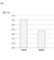
本発明による積層セラミックコンデンサについて、振動音を抑制する効果の確認試験を実施した。
本発明による積層セラミックコンデンサについて、振動音を抑制する効果の確認試験を実施した。
確認試験は、本発明の外部電極表面の所定範囲に絶縁層を配置した積層セラミックコンデンサをサンプルとした実施例と従来の絶縁層を備えない積層セラミックコンデンサをサンプルとした比較例について、直流3Vと交流1Vを印加した際に生じる振動音の音圧(dB)を測定した。
図6に示すように、本発明の積層セラミックコンデンサ(実施例)においては、配線基板に実装した際に生じる圧電現象を起因とする誘電体の振動を抑え、耳障りな振動音を低減することを確認することができた。
以上、本発明の実施形態について説明したが、本発明は実施形態に限定されるものではなく、本発明の要旨を逸脱しない範囲において種々の態様で実施することが可能である。例えば、実施形態は、第1外部電極4aと第2外部電極4bの双方に絶縁層8を設けた例を示したが、第1外部電極4aと第2外部電極4bのいずれかに絶縁層8を設けた場合にも同様の効果を得ることが期待できる。
本発明は以下のとおりである。
<1>
誘電体層と内部電極層とが交互に積層された積層体と、前記積層体の積層方向と直交する長さ方向の両側の端面にそれぞれ配置され且つ前記内部電極層と接続された外部電極と、を有する積層セラミックコンデンサであって、
前記外部電極は、前記長さ方向から平面視したときの表面を、外周縁から幅1μm以上100μm以下の枠領域を除き、絶縁層で覆われている、積層セラミックコンデンサ。
<2>
前記外部電極は、前記長さ方向から平面視したときの前記内部電極層が積層する領域に相当する表面を前記絶縁層で覆われている、<1>記載の積層セラミックコンデンサ。
<3>
前記絶縁層は、前記長さ方向の厚みが200μm以下であり、前記長さ方向から見た略中央において最も厚い形状である、<1>又は<2>記載の積層セラミックコンデンサ。
<4>
<1>乃至<3>のいずれかに記載される積層セラミックコンデンサと、配線基板上に配置されたランドと、前記積層セラミックコンデンサの前記外部電極と前記ランドを接続するはんだと、を備えた実装構造であって、前記はんだが前記絶縁層より下方に配置されている、積層セラミックコンデンサの実装構造。
1 積層セラミックコンデンサ
2 積層体
3 内層部
4 外部電極
4a 第1外部電極
4b 第2外部電極
5 誘電体層
5a 誘電体層
5b 誘電体層
6 内部電極層
6a 第1内部電極層
6b 第2内部電極層
7 外層部
8 絶縁層
9 枠領域
41a 第1下地電極層
41b 第2下地電極層
42a 第1めっき層
42b 第2めっき層
421a Niめっき層
421b Niめっき層
422a Snめっき層
422b Snめっき層
50 配線基板
51a ランド
51b ランド
52a はんだフィレット
52b はんだフィレット
TS1 第1主面
TS2 第2主面
WS1 第1側面
WS2 第2側面
LS1 第1端面
LS2 第2端面
Claims (4)
- 誘電体層と内部電極層とが交互に積層された積層体と、前記積層体の積層方向と直交する長さ方向の両側の端面にそれぞれ配置され且つ前記内部電極層と接続された外部電極と、を有する積層セラミックコンデンサであって、
前記外部電極は、前記長さ方向から平面視したときの表面を、外周縁から幅1μm以上100μm以下の枠領域を除き、絶縁層で覆われている、積層セラミックコンデンサ。 - 前記外部電極は、前記長さ方向から平面視したときの前記内部電極層が積層する領域に相当する表面を前記絶縁層で覆われている、請求項1記載の積層セラミックコンデンサ。
- 前記絶縁層は、前記長さ方向の厚みが200μm以下であり、前記長さ方向から見た略中央において最も厚い形状である、請求項1又は2記載の積層セラミックコンデンサ。
- 請求項1乃至請求項3のいずれかに記載される積層セラミックコンデンサと、配線基板上に配置されたランドと、前記積層セラミックコンデンサの前記外部電極と前記ランドを接続するはんだと、を備えた実装構造であって、前記はんだが前記絶縁層より下方に配置されている、積層セラミックコンデンサの実装構造。
Applications Claiming Priority (2)
| Application Number | Priority Date | Filing Date | Title |
|---|---|---|---|
| JP2022-130642 | 2022-08-18 | ||
| JP2022130642 | 2022-08-18 |
Publications (1)
| Publication Number | Publication Date |
|---|---|
| WO2024038650A1 true WO2024038650A1 (ja) | 2024-02-22 |
Family
ID=89941700
Family Applications (1)
| Application Number | Title | Priority Date | Filing Date |
|---|---|---|---|
| PCT/JP2023/019394 WO2024038650A1 (ja) | 2022-08-18 | 2023-05-24 | 積層セラミックコンデンサ |
Country Status (1)
| Country | Link |
|---|---|
| WO (1) | WO2024038650A1 (ja) |
Citations (3)
| Publication number | Priority date | Publication date | Assignee | Title |
|---|---|---|---|---|
| JPH02155209A (ja) * | 1988-12-07 | 1990-06-14 | Nec Corp | 表面実装用チップ部品 |
| JP2015053503A (ja) * | 2012-10-26 | 2015-03-19 | サムソン エレクトロ−メカニックス カンパニーリミテッド. | 積層チップ電子部品及びその実装基板 |
| JP2016105488A (ja) * | 2015-12-16 | 2016-06-09 | Tdk株式会社 | セラミック電子部品のはんだ実装構造 |
-
2023
- 2023-05-24 WO PCT/JP2023/019394 patent/WO2024038650A1/ja unknown
Patent Citations (3)
| Publication number | Priority date | Publication date | Assignee | Title |
|---|---|---|---|---|
| JPH02155209A (ja) * | 1988-12-07 | 1990-06-14 | Nec Corp | 表面実装用チップ部品 |
| JP2015053503A (ja) * | 2012-10-26 | 2015-03-19 | サムソン エレクトロ−メカニックス カンパニーリミテッド. | 積層チップ電子部品及びその実装基板 |
| JP2016105488A (ja) * | 2015-12-16 | 2016-06-09 | Tdk株式会社 | セラミック電子部品のはんだ実装構造 |
Similar Documents
| Publication | Publication Date | Title |
|---|---|---|
| JP6395002B2 (ja) | 積層セラミックキャパシタの回路基板実装構造 | |
| JP7136427B2 (ja) | 積層セラミック電子部品及びその実装基板 | |
| JP5536244B2 (ja) | 積層セラミックキャパシタ、積層セラミックキャパシタの回路基板実装構造及び積層セラミックキャパシタの包装体 | |
| JP5485351B2 (ja) | 積層チップ電子部品、その実装基板及び包装体 | |
| US9653214B2 (en) | Laminated capacitor and laminated capacitor series and laminated capacitor mounted body including capacitor | |
| KR102029495B1 (ko) | 칩 전자부품 및 그 실장 기판 | |
| KR102516763B1 (ko) | 복합 전자부품, 그 실장 기판 | |
| JP5694409B2 (ja) | 積層セラミックキャパシタ及び積層セラミックキャパシタの実装基板 | |
| KR20210130648A (ko) | 적층 세라믹 콘덴서 | |
| KR20210131240A (ko) | 적층 세라믹 콘덴서 | |
| JP2015015445A (ja) | 積層セラミックキャパシタ及びその実装基板並びに製造方法 | |
| CN109817452B (zh) | 复合电子组件和具有其的板 | |
| US11955281B2 (en) | Electronic component and board for mounting the same | |
| US10770235B2 (en) | Multilayer capacitor | |
| JP6483400B2 (ja) | 積層型コンデンサおよび実装構造 | |
| KR20210130645A (ko) | 적층 세라믹 콘덴서 | |
| WO2024038650A1 (ja) | 積層セラミックコンデンサ | |
| JP2020057752A (ja) | 複合電子部品 | |
| JP2013026508A (ja) | コンデンサおよび回路基板 | |
| KR102319605B1 (ko) | 복합 전자부품 | |
| KR20180008821A (ko) | 적층 세라믹 커패시터 및 그 실장 기판 | |
| KR102109639B1 (ko) | 적층 세라믹 전자 부품 및 그 실장 기판 | |
| KR102620525B1 (ko) | 적층형 커패시터 | |
| JP2016001694A (ja) | 積層コンデンサ、これを含む積層コンデンサ連および積層コンデンサ実装体 | |
| JP2023118477A (ja) | 積層セラミック電子部品 |
Legal Events
| Date | Code | Title | Description |
|---|---|---|---|
| 121 | Ep: the epo has been informed by wipo that ep was designated in this application |
Ref document number: 23854689 Country of ref document: EP Kind code of ref document: A1 |