WO2024038650A1 - 積層セラミックコンデンサ - Google Patents
積層セラミックコンデンサ Download PDFInfo
- Publication number
- WO2024038650A1 WO2024038650A1 PCT/JP2023/019394 JP2023019394W WO2024038650A1 WO 2024038650 A1 WO2024038650 A1 WO 2024038650A1 JP 2023019394 W JP2023019394 W JP 2023019394W WO 2024038650 A1 WO2024038650 A1 WO 2024038650A1
- Authority
- WO
- WIPO (PCT)
- Prior art keywords
- layer
- ceramic capacitor
- multilayer ceramic
- electrode layer
- internal electrode
- Prior art date
- Legal status (The legal status is an assumption and is not a legal conclusion. Google has not performed a legal analysis and makes no representation as to the accuracy of the status listed.)
- Ceased
Links
Images


Classifications
-
- H—ELECTRICITY
- H01—ELECTRIC ELEMENTS
- H01G—CAPACITORS; CAPACITORS, RECTIFIERS, DETECTORS, SWITCHING DEVICES, LIGHT-SENSITIVE OR TEMPERATURE-SENSITIVE DEVICES OF THE ELECTROLYTIC TYPE
- H01G4/00—Fixed capacitors; Processes of their manufacture
- H01G4/002—Details
- H01G4/228—Terminals
- H01G4/232—Terminals electrically connecting two or more layers of a stacked or rolled capacitor
-
- H—ELECTRICITY
- H01—ELECTRIC ELEMENTS
- H01G—CAPACITORS; CAPACITORS, RECTIFIERS, DETECTORS, SWITCHING DEVICES, LIGHT-SENSITIVE OR TEMPERATURE-SENSITIVE DEVICES OF THE ELECTROLYTIC TYPE
- H01G2/00—Details of capacitors not covered by a single one of groups H01G4/00-H01G11/00
- H01G2/02—Mountings
- H01G2/06—Mountings specially adapted for mounting on a printed-circuit support
- H01G2/065—Mountings specially adapted for mounting on a printed-circuit support for surface mounting, e.g. chip capacitors
-
- H—ELECTRICITY
- H01—ELECTRIC ELEMENTS
- H01G—CAPACITORS; CAPACITORS, RECTIFIERS, DETECTORS, SWITCHING DEVICES, LIGHT-SENSITIVE OR TEMPERATURE-SENSITIVE DEVICES OF THE ELECTROLYTIC TYPE
- H01G4/00—Fixed capacitors; Processes of their manufacture
- H01G4/002—Details
- H01G4/005—Electrodes
- H01G4/012—Form of non-self-supporting electrodes
-
- H—ELECTRICITY
- H01—ELECTRIC ELEMENTS
- H01G—CAPACITORS; CAPACITORS, RECTIFIERS, DETECTORS, SWITCHING DEVICES, LIGHT-SENSITIVE OR TEMPERATURE-SENSITIVE DEVICES OF THE ELECTROLYTIC TYPE
- H01G4/00—Fixed capacitors; Processes of their manufacture
- H01G4/002—Details
- H01G4/018—Dielectrics
- H01G4/06—Solid dielectrics
- H01G4/08—Inorganic dielectrics
- H01G4/12—Ceramic dielectrics
- H01G4/1209—Ceramic dielectrics characterised by the ceramic dielectric material
- H01G4/1218—Ceramic dielectrics characterised by the ceramic dielectric material based on titanium oxides or titanates
- H01G4/1227—Ceramic dielectrics characterised by the ceramic dielectric material based on titanium oxides or titanates based on alkaline earth titanates
-
- H—ELECTRICITY
- H01—ELECTRIC ELEMENTS
- H01G—CAPACITORS; CAPACITORS, RECTIFIERS, DETECTORS, SWITCHING DEVICES, LIGHT-SENSITIVE OR TEMPERATURE-SENSITIVE DEVICES OF THE ELECTROLYTIC TYPE
- H01G4/00—Fixed capacitors; Processes of their manufacture
- H01G4/002—Details
- H01G4/228—Terminals
- H01G4/232—Terminals electrically connecting two or more layers of a stacked or rolled capacitor
- H01G4/2325—Terminals electrically connecting two or more layers of a stacked or rolled capacitor characterised by the material of the terminals
-
- H—ELECTRICITY
- H01—ELECTRIC ELEMENTS
- H01G—CAPACITORS; CAPACITORS, RECTIFIERS, DETECTORS, SWITCHING DEVICES, LIGHT-SENSITIVE OR TEMPERATURE-SENSITIVE DEVICES OF THE ELECTROLYTIC TYPE
- H01G4/00—Fixed capacitors; Processes of their manufacture
- H01G4/002—Details
- H01G4/228—Terminals
- H01G4/252—Terminals the terminals being coated on the capacitive element
-
- H—ELECTRICITY
- H01—ELECTRIC ELEMENTS
- H01G—CAPACITORS; CAPACITORS, RECTIFIERS, DETECTORS, SWITCHING DEVICES, LIGHT-SENSITIVE OR TEMPERATURE-SENSITIVE DEVICES OF THE ELECTROLYTIC TYPE
- H01G4/00—Fixed capacitors; Processes of their manufacture
- H01G4/30—Stacked capacitors
-
- Y—GENERAL TAGGING OF NEW TECHNOLOGICAL DEVELOPMENTS; GENERAL TAGGING OF CROSS-SECTIONAL TECHNOLOGIES SPANNING OVER SEVERAL SECTIONS OF THE IPC; TECHNICAL SUBJECTS COVERED BY FORMER USPC CROSS-REFERENCE ART COLLECTIONS [XRACs] AND DIGESTS
- Y02—TECHNOLOGIES OR APPLICATIONS FOR MITIGATION OR ADAPTATION AGAINST CLIMATE CHANGE
- Y02E—REDUCTION OF GREENHOUSE GAS [GHG] EMISSIONS, RELATED TO ENERGY GENERATION, TRANSMISSION OR DISTRIBUTION
- Y02E60/00—Enabling technologies; Technologies with a potential or indirect contribution to GHG emissions mitigation
- Y02E60/13—Energy storage using capacitors
Definitions
- the present invention relates to a multilayer ceramic capacitor that can suppress the generation of vibration noise caused by piezoelectric phenomena during mounting.
- a multilayer ceramic capacitor is composed of a rectangular parallelepiped-shaped laminate in which dielectric layers and internal electrode layers are alternately laminated, and external electrodes formed at opposing ends of the laminate.
- the dielectric that constitutes the dielectric layer is usually a dielectric ceramic with a perovskite structure such as barium titanate, so if an alternating current voltage is applied while a direct current voltage is applied, vibrations occur due to piezoelectric phenomena. Therefore, when a multilayer ceramic capacitor is mounted on a wiring board and, for example, an AC voltage in the audible frequency band of 20Hz to 20kHz is applied to the external electrode, the multilayer ceramic capacitor expands and contracts and vibrates, causing the surrounding air to vibrate and produce sound. When this occurs, the wiring board also vibrates resonantly, causing the problem that the sound is amplified and becomes harsh.
- An object of the present invention is to provide a multilayer ceramic capacitor that can suppress vibrations of a dielectric material caused by piezoelectric phenomena that occur when mounted on a wiring board, and can reduce harsh vibration noise.
- the present inventor discovered that by arranging an insulator at a predetermined position of the external electrode of a multilayer ceramic capacitor, it is possible to suppress the vibration noise caused by the piezoelectric phenomenon that occurs when the capacitor is mounted, and was able to complete the present invention. Ta.
- the present invention provides a laminate in which dielectric layers and internal electrode layers are alternately laminated, and a laminate in which dielectric layers and internal electrode layers are arranged on both end faces of the laminate in a longitudinal direction perpendicular to the lamination direction and connected to the internal electrode layers.
- a multilayer ceramic capacitor having an external electrode The external electrode is a multilayer ceramic capacitor whose surface, when viewed in plan from the longitudinal direction, is covered with an insulating layer except for a frame region having a width of 1 ⁇ m or more and 100 ⁇ m or less from the outer periphery.
- the present invention it is possible to provide a multilayer ceramic capacitor that can suppress vibrations of a dielectric material caused by piezoelectric phenomena that occur when mounted on a wiring board, and can reduce unpleasant vibration noise.
- FIG. 2 is an external view of a multilayer ceramic capacitor. 2 is a cross-sectional view taken along line AA of the multilayer ceramic capacitor shown in FIG. 1.
- FIG. FIG. 3 is an exploded perspective view schematically showing an example of an inner layer part. 1 is an external view showing an example of a mounting state of a multilayer ceramic capacitor according to the present invention.
- FIG. 2 is an external view showing an example of a mounting state of a conventional multilayer ceramic capacitor.
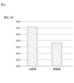
- FIG. 3 is a diagram showing the effect of reducing vibration noise of the multilayer ceramic capacitor according to the present invention.
- FIG. 1 is an external view of a multilayer ceramic capacitor 1.
- FIG. 2 is a cross-sectional view (LT cross-sectional view) of the multilayer ceramic capacitor 1 taken along the line AA at the center in the width direction W shown in FIG.
- FIG. 3 is a schematic diagram showing the structure of the inner layer portion 3.
- the direction in which the dielectric layers and internal electrode layers are laminated is defined as the lamination direction T
- the length direction L is perpendicular to the lamination direction T
- the width direction W is perpendicular to the lamination direction T and the length direction L.
- the structure of the ceramic capacitor 1 will be described.
- the width direction W, the length direction L, and the lamination direction T are orthogonal to each other, but they are not necessarily orthogonal to each other, and may be intersecting to each other.
- the multilayer ceramic capacitor 1 includes a multilayer body 2 having a rectangular parallelepiped shape.
- the laminate 2 includes an inner layer part 3, and has a pair of first main surfaces TS1 and second main surfaces TS2 facing each other in the stacking direction T, and a pair of first main surfaces TS1 and second main surfaces TS2 facing each other in the length direction L perpendicular to the stacking direction T. It has a pair of first end surfaces LS1 and a second end surface LS2, and a pair of first side surfaces WS1 and second side surfaces WS2 that face each other in the width direction W perpendicular to both the stacking direction T and the length direction L. ing.
- the dimensions of the multilayer ceramic capacitor 1 are not particularly limited, but for example, the dimensions in the stacking direction T are about 0.1 mm to 2.5 mm, and the dimensions in the length direction L are about 0.1 mm to 3.2 mm.
- the dimension in the width direction W can be approximately 0.1 mm to 2.5 mm.
- the inner layer portion 3 is composed of a plurality of dielectric layers 5 and a plurality of internal electrode layers 6 stacked together.
- the internal electrode layer 6 is composed of a first internal electrode layer 6a and a second internal electrode layer 6b.
- the first internal electrode layer 6a and the second internal electrode layer 6b are arranged on the dielectric layers 5a and 5b, respectively.
- the internal electrode layer 6 extends in the length direction L and has a rectangular shape when viewed in plan from the stacking direction T.
- the first internal electrode layer 6a is drawn out to the first end surface LS1 of the laminate 2
- the second internal electrode layer 6b is drawn out to the second end surface LS2 of the laminate 2.
- the dielectric layer 5 is made of a dielectric material.
- a dielectric ceramic containing components such as BaTiO 3 , CaTiO 3 , SrTiO 3 , or CaZrO 3 can be used.
- the dielectric material may be one in which subcomponents such as Mn compounds, Fe compounds, Cr compounds, Co compounds, and Ni compounds are added to these main components.
- the thickness of the dielectric layer 5 is not particularly limited, but is, for example, 0.3 ⁇ m to 2.0 ⁇ m in the effective region of capacitance formation formed by the first internal electrode layer 6a and the second internal electrode layer 6b. It can be about 0 ⁇ m.
- the number of layers of the dielectric layer 5 is not particularly limited, but for example, in the effective area of capacitance formation formed by the first internal electrode layer 6a and the second internal electrode layer 6b, the number of layers is 1 to 6000 layers. It can be done.
- an outer layer portion 7 is provided, which is composed only of the dielectric layer 5 without the internal electrode layer 6 formed thereon.
- the thickness of the outer layer portion 7 is not limited, but may be, for example, 15 ⁇ m to 150 ⁇ m. Note that the thickness of the dielectric layer in the outer layer portion 7 may be larger than the thickness of the dielectric layer in the effective area for forming capacitance where the internal electrode layer 6 is formed. Further, the material of the dielectric layer in the outer layer portion may be different from the material of the dielectric layer in the inner layer portion.
- FIG. 3 shows the inner layer portion 3 broken down into dielectric layers 5 in the stacking direction T.
- the internal electrode layer 6 is formed by sintering a conductive paste containing a metal powder serving as a conductor, an organic solvent, a binder, and a dispersant on the dielectric layer.
- the internal electrode layers 6 and the dielectric layers 5 are alternately laminated to form the inner layer portion 3.
- the internal electrode layer 6 is composed of a first internal electrode layer 6a and a second internal electrode layer 6b, and the first internal electrode layer 6a and the second internal electrode layer 6b are arranged on the dielectric layers 5a and 5b, respectively. ing.
- metals such as Ni, Cu, Ag, Pd, Ag-Pd alloy, and Au can be used. Further, these metals may be compounds containing these metal elements or alloys with other metals.
- the thickness of the internal electrode layer 6 is not particularly limited, but may be, for example, about 0.3 ⁇ m to 1.5 ⁇ m.
- a first external electrode 4a and a second external electrode 4b are formed on the first end surface LS1 and the second end surface LS2 of the laminate 2, respectively.
- the first external electrode 4a includes a first base electrode layer 41a and a first plating layer 42a disposed on the first base electrode layer 41a.
- the second external electrode 4b includes a second base electrode layer 41b and a second plating layer 42b disposed on the second base electrode layer 41b.
- the first base electrode layer 41a is arranged on the first end surface LS1.
- the first base electrode layer 41a is connected to the first internal electrode layer 6a.
- the first base electrode layer 41a extends from above the first end surface LS1 to a part of the first main surface TS1 and a part of the second main surface TS2, and a part of the first side surface WS1 and the second side surface. It is formed to extend to a part of WS2.
- the second base electrode layer 41b is arranged on the second end surface LS2.
- the second base electrode layer 41b is connected to the second internal electrode layer 6b.
- the second base electrode layer 41b extends from above the second end surface LS2 to a part of the first main surface TS1 and a part of the second main surface TS2, and a part of the first side surface WS1 and the second side surface. It is formed to extend to a part of WS2.
- the first base electrode layer 41a and the second base electrode layer 41b include at least one selected from a baked layer, a conductive resin layer, a thin film layer, and the like.
- the first base electrode layer 41a and the second base electrode layer 41b of this embodiment are baked layers.
- the baking layer contains a metal component and either a glass component or a ceramic component, or both.
- the metal component includes, for example, at least one selected from Cu, Ni, Ag, Pd, Ag-Pd alloy, Au, and the like.
- the glass component includes, for example, at least one selected from B, Si, Ba, Mg, Al, Li, and the like.
- the ceramic component the same type of ceramic material as the dielectric layer 5 may be used, or a different type of ceramic material may be used.
- the ceramic component includes, for example, at least one selected from BaTiO 3 , CaTiO 3 , (Ba,Ca)TiO 3 , SrTiO 3 , CaZrO 3 , and the like.
- the baked layer is, for example, a layered product coated with a conductive paste containing glass and metal and baked.
- the baked layer may be obtained by simultaneously firing a multilayer chip having an internal electrode layer and a dielectric layer and a conductive paste applied to the multilayer chip, or by baking a multilayer chip having an internal electrode layer and a dielectric layer to create a multilayer product. After obtaining the laminate, a conductive paste may be applied to the laminate and baked.
- the baked layer is formed by baking a ceramic material added instead of a glass component. It is preferable to do so. In this case, it is particularly preferable to use the same type of ceramic material as the dielectric layer as the added ceramic material.
- the baking layer may have multiple layers.
- the thickness in the length direction L of the first base electrode layer 41a located on the first end surface LS1 is, for example, about 3 ⁇ m or more and 160 ⁇ m or less at the center of the first base electrode layer 41a in the stacking direction T and width direction W. It is preferable.
- the thickness in the length direction L of the second base electrode layer 41b located on the second end surface LS2 is, for example, about 3 ⁇ m or more and 160 ⁇ m or less at the center of the second base electrode layer 41b in the stacking direction T and width direction W. It is preferable.
- the stacking direction T of the first base electrode layer 41a provided on this part is The thickness of the first base electrode layer 41a provided in this portion is preferably about 3 ⁇ m or more and 40 ⁇ m or less at the central portion in the length direction L and width direction W, for example.
- the thickness in the width direction W of the first base electrode layer 41a provided on this part is preferably, for example, approximately 3 ⁇ m or more and 40 ⁇ m or less in the center portion of the first base electrode layer 41a provided in this portion in the length direction L and the stacking direction T.
- the stacking direction T of the second base electrode layer 41b provided on this part is preferably about 3 ⁇ m or more and 40 ⁇ m or less at the central portion in the length direction L and width direction W, for example.
- the thickness in the width direction W of the second base electrode layer 41b provided on this part is preferably, for example, approximately 3 ⁇ m or more and 40 ⁇ m or less in the central portion of the second base electrode layer 41b provided in this portion in the length direction L and the stacking direction T.
- a configuration may be adopted in which a first plating layer 42a and a second plating layer 42b, which will be described later, are directly arranged on the laminate 2 without providing the first base electrode layer 41a and the second base electrode layer 41b.
- the first base electrode layer 41a and the second base electrode layer 41b are not limited to baked layers, but may be thin film layers.
- the thin film layer is formed by a thin film forming method such as a sputtering method or a vapor deposition method.
- the thin film layer is a layer of 1 ⁇ m or less on which metal particles are deposited.
- the first plating layer 42a is arranged to cover the first base electrode layer 41a.
- the second plating layer 42b is arranged to cover the second base electrode layer 41b.
- the first plating layer 42a and the second plating layer 42b may contain, for example, at least one selected from Cu, Ni, Sn, Ag, Pd, Ag-Pd alloy, Au, and the like.
- the first plating layer 42a and the second plating layer 42b may each be formed of multiple layers.
- the first plating layer 42a and the second plating layer 42b preferably have a two-layer structure in which Sn plating layers 422a and 422b are formed on Ni plating layers 421a and 421b, respectively.
- the Ni plating layers 421a and 421b prevent the first base electrode layer 41a and the second base electrode layer 41b from being eroded by solder when mounting the multilayer ceramic capacitor 1.
- the Sn plating layer improves solder wettability when mounting the multilayer ceramic capacitor 1. This facilitates mounting of the multilayer ceramic capacitor 1.
- the thickness of each of the Ni plating layer and the Sn plating layer should be 2 ⁇ m or more and 15 ⁇ m or less. preferable.
- the surfaces of the first external electrode 4a and the second external electrode 4b when viewed in plan from the length direction L are covered with an insulating layer 8 except for a frame region 9 having a width of 1 ⁇ m or more and 100 ⁇ m or less from the outer periphery.
- the insulating layer can be placed in a predetermined range on the surface of the plating layer.
- the plating layer is formed on the surface of the base electrode layer except for the area where the insulating layer is disposed.
- an insulating layer can be placed in a predetermined range on the surface of the outermost plating layer, but an insulating layer can be placed on the surface of any plating layer other than the outermost layer.
- the plating layer should be stacked on the part excluding the area where the insulating layer is placed, and the plating layer should be placed on the part where the insulating layer is placed, and the plating layer should be placed on the part where the insulating layer is placed, and the plating layer should be stacked on the part of the plating layer that is placed on the plating layer where the insulating layer is placed.
- the structure is such that an insulating layer is disposed on the surface.
- An insulating layer 8 is formed on the surface of the outer peripheral edge excluding a frame region 9 having a width of 1 ⁇ m or more and 100 ⁇ m or less, and a first base electrode layer 41a and a second base electrode layer excluding the area where the insulating layer 8 is disposed.
- Ni plating layers 421a, 421b and Sn plating layers 422a, 422b are formed on the surface of 41b.
- the multilayer ceramic capacitor 1 is connected to lands 51a and 51b by applying solder to the surfaces of the first external electrode 4a and the second external electrode 4b below the insulating layer 8.
- solder By providing the frame region 9, a solder fillet can be formed within a certain height range from below the outer periphery, so that bonding to the wiring board can be performed reliably.
- the material of the insulating layer 8 is not particularly limited as long as it has insulating properties, but it is preferable to use a synthetic resin because the insulating layer can be easily formed on the surface of the external electrode.
- a synthetic resin thermosetting resins such as epoxy resins, polyimide resins, and phenol resins, and thermoplastic resins such as polyethylene resins and polyamide resins can be used.
- the internal It is possible to prevent the solder fillets 52a and 52b from getting wet up to the height at which the electrode layer 6 is arranged. Thereby, generation of vibration noise caused by piezoelectric phenomenon can be effectively suppressed.
- the insulating layer 8 has a thickness in the length direction L of 200 ⁇ m or less, and is thickest at approximately the center when viewed from the length direction L. This prevents the multilayer ceramic capacitor from increasing in size, and when it is mounted on a wiring board, the center part of the surface of the insulating layer protrudes outward from the bottom part, which reduces wetting of the solder fillet. This makes it possible to reliably prevent this.
- the multilayer ceramic capacitor 1 is mounted by applying solder to the surfaces of the first external electrode 4a and the second external electrode 4b and connecting them to the lands 51a and 51b. As shown, when the wetting height of the solder fillets 52a and 52b formed during mounting is high and reaches the height at which the internal electrode layer 6 is arranged, a piezoelectric phenomenon of the dielectric occurs, and the expansion and contraction vibration of the multilayer ceramic capacitor 1 occurs. is likely to occur.
- FIG. 4 shows a mounting example of the multilayer ceramic capacitor 1 according to this embodiment.
- the insulating layer 8 is provided in a predetermined range on the surfaces of the first external electrode 4a and the second external electrode 4b, the height at which the solder fillets 52a and 52b are wetted is suppressed to a low level, and the piezoelectric phenomenon is suppressed. The generation of vibration noise caused by this can be suppressed.
- the multilayer ceramic capacitor (example) of the present invention it is possible to suppress the vibration of the dielectric material caused by the piezoelectric phenomenon that occurs when it is mounted on a wiring board, and to reduce the harsh vibration noise. I was able to confirm.
- the present invention is not limited to the embodiments, and can be implemented in various forms without departing from the gist of the present invention.
- the embodiment has shown an example in which the insulating layer 8 is provided on both the first external electrode 4a and the second external electrode 4b, the insulating layer 8 is provided on either the first external electrode 4a or the second external electrode 4b. Similar effects can be expected to be obtained when
- the present invention is as follows.
- ⁇ 1> A laminate in which dielectric layers and internal electrode layers are alternately laminated; and external electrodes arranged on both end faces of the laminate in a longitudinal direction perpendicular to the lamination direction and connected to the internal electrode layers.
- a multilayer ceramic capacitor having In the multilayer ceramic capacitor, the surface of the external electrode when viewed in plan from the length direction is covered with an insulating layer except for a frame region having a width of 1 ⁇ m or more and 100 ⁇ m or less from the outer periphery.
- ⁇ 2> The multilayer ceramic capacitor according to ⁇ 1>, wherein a surface of the external electrode corresponding to a region where the internal electrode layer is laminated when viewed in plan from the length direction is covered with the insulating layer.
- ⁇ 3> The multilayer ceramic capacitor according to ⁇ 1> or ⁇ 2>, wherein the insulating layer has a thickness of 200 ⁇ m or less in the length direction, and is thickest at approximately the center when viewed from the length direction.
- a mounting comprising the multilayer ceramic capacitor according to any one of ⁇ 1> to ⁇ 3>, a land arranged on a wiring board, and a solder connecting the external electrode and the land of the multilayer ceramic capacitor.
- Multilayer ceramic capacitor 2 Laminated body 3 Inner layer portion 4 External electrode 4a First external electrode 4b Second external electrode 5 Dielectric layer 5a Dielectric layer 5b Dielectric layer 6 Internal electrode layer 6a First internal electrode layer 6b Second internal electrode Layer 7 Outer layer 8 Insulating layer 9 Frame region 41a First base electrode layer 41b Second base electrode layer 42a First plating layer 42b Second plating layer 421a Ni plating layer 421b Ni plating layer 422a Sn plating layer 422b Sn plating layer 50 Wiring Substrate 51a Land 51b Land 52a Solder fillet 52b Solder fillet TS1 First main surface TS2 Second main surface WS1 First side surface WS2 Second side surface LS1 First end surface LS2 Second end surface
Landscapes
- Engineering & Computer Science (AREA)
- Power Engineering (AREA)
- Microelectronics & Electronic Packaging (AREA)
- Manufacturing & Machinery (AREA)
- Chemical & Material Sciences (AREA)
- Ceramic Engineering (AREA)
- Inorganic Chemistry (AREA)
- Ceramic Capacitors (AREA)
- Fixed Capacitors And Capacitor Manufacturing Machines (AREA)
Priority Applications (4)
| Application Number | Priority Date | Filing Date | Title |
|---|---|---|---|
| JP2024541422A JP7816535B2 (ja) | 2022-08-18 | 2023-05-24 | 積層セラミックコンデンサ |
| CN202380048078.8A CN119422214A (zh) | 2022-08-18 | 2023-05-24 | 层叠陶瓷电容器 |
| KR1020247039860A KR20250002709A (ko) | 2022-08-18 | 2023-05-24 | 적층 세라믹 콘덴서 |
| US18/760,091 US20240355546A1 (en) | 2022-08-18 | 2024-07-01 | Multilayer ceramic capacitor |
Applications Claiming Priority (2)
| Application Number | Priority Date | Filing Date | Title |
|---|---|---|---|
| JP2022130642 | 2022-08-18 | ||
| JP2022-130642 | 2022-08-18 |
Related Child Applications (1)
| Application Number | Title | Priority Date | Filing Date |
|---|---|---|---|
| US18/760,091 Continuation US20240355546A1 (en) | 2022-08-18 | 2024-07-01 | Multilayer ceramic capacitor |
Publications (1)
| Publication Number | Publication Date |
|---|---|
| WO2024038650A1 true WO2024038650A1 (ja) | 2024-02-22 |
Family
ID=89941700
Family Applications (1)
| Application Number | Title | Priority Date | Filing Date |
|---|---|---|---|
| PCT/JP2023/019394 Ceased WO2024038650A1 (ja) | 2022-08-18 | 2023-05-24 | 積層セラミックコンデンサ |
Country Status (5)
| Country | Link |
|---|---|
| US (1) | US20240355546A1 (https=) |
| JP (1) | JP7816535B2 (https=) |
| KR (1) | KR20250002709A (https=) |
| CN (1) | CN119422214A (https=) |
| WO (1) | WO2024038650A1 (https=) |
Citations (3)
| Publication number | Priority date | Publication date | Assignee | Title |
|---|---|---|---|---|
| JPH02155209A (ja) * | 1988-12-07 | 1990-06-14 | Nec Corp | 表面実装用チップ部品 |
| JP2015053503A (ja) * | 2012-10-26 | 2015-03-19 | サムソン エレクトロ−メカニックス カンパニーリミテッド. | 積層チップ電子部品及びその実装基板 |
| JP2016105488A (ja) * | 2015-12-16 | 2016-06-09 | Tdk株式会社 | セラミック電子部品のはんだ実装構造 |
Family Cites Families (10)
| Publication number | Priority date | Publication date | Assignee | Title |
|---|---|---|---|---|
| JP2000182888A (ja) | 1998-12-16 | 2000-06-30 | Taiyo Yuden Co Ltd | 積層セラミックコンデンサ |
| JP4093188B2 (ja) | 2003-05-27 | 2008-06-04 | 株式会社村田製作所 | 積層セラミック電子部品とその実装構造および実装方法 |
| JP2013058558A (ja) * | 2011-09-07 | 2013-03-28 | Tdk Corp | 電子部品 |
| JP6449529B2 (ja) | 2012-08-09 | 2019-01-09 | Tdk株式会社 | 電子部品 |
| KR101422929B1 (ko) * | 2012-11-07 | 2014-07-23 | 삼성전기주식회사 | 적층 세라믹 전자부품 및 그 실장 기판 |
| KR101548793B1 (ko) * | 2013-01-14 | 2015-08-31 | 삼성전기주식회사 | 적층 세라믹 커패시터, 적층 세라믹 커패시터의 실장 기판 및 적층 세라믹 커패시터의 제조 방법 |
| KR101823246B1 (ko) * | 2016-06-21 | 2018-01-29 | 삼성전기주식회사 | 적층 세라믹 전자 부품 및 그 실장 기판 |
| KR101883061B1 (ko) * | 2016-09-08 | 2018-07-27 | 삼성전기주식회사 | 적층 세라믹 전자부품 및 그 제조방법 |
| JP2021068853A (ja) * | 2019-10-28 | 2021-04-30 | 株式会社村田製作所 | 支持端子付きコンデンサチップ |
| JP2023019368A (ja) * | 2021-07-29 | 2023-02-09 | 株式会社村田製作所 | 積層セラミックコンデンサ |
-
2023
- 2023-05-24 JP JP2024541422A patent/JP7816535B2/ja active Active
- 2023-05-24 KR KR1020247039860A patent/KR20250002709A/ko not_active Ceased
- 2023-05-24 CN CN202380048078.8A patent/CN119422214A/zh active Pending
- 2023-05-24 WO PCT/JP2023/019394 patent/WO2024038650A1/ja not_active Ceased
-
2024
- 2024-07-01 US US18/760,091 patent/US20240355546A1/en active Pending
Patent Citations (3)
| Publication number | Priority date | Publication date | Assignee | Title |
|---|---|---|---|---|
| JPH02155209A (ja) * | 1988-12-07 | 1990-06-14 | Nec Corp | 表面実装用チップ部品 |
| JP2015053503A (ja) * | 2012-10-26 | 2015-03-19 | サムソン エレクトロ−メカニックス カンパニーリミテッド. | 積層チップ電子部品及びその実装基板 |
| JP2016105488A (ja) * | 2015-12-16 | 2016-06-09 | Tdk株式会社 | セラミック電子部品のはんだ実装構造 |
Also Published As
| Publication number | Publication date |
|---|---|
| KR20250002709A (ko) | 2025-01-07 |
| JPWO2024038650A1 (https=) | 2024-02-22 |
| CN119422214A (zh) | 2025-02-11 |
| JP7816535B2 (ja) | 2026-02-18 |
| US20240355546A1 (en) | 2024-10-24 |
Similar Documents
| Publication | Publication Date | Title |
|---|---|---|
| JP7567146B2 (ja) | 積層セラミック電子部品及びその実装基板 | |
| JP6395002B2 (ja) | 積層セラミックキャパシタの回路基板実装構造 | |
| CN110265216B (zh) | 多层电子组件及具有多层电子组件的板 | |
| JP5536244B2 (ja) | 積層セラミックキャパシタ、積層セラミックキャパシタの回路基板実装構造及び積層セラミックキャパシタの包装体 | |
| US9653214B2 (en) | Laminated capacitor and laminated capacitor series and laminated capacitor mounted body including capacitor | |
| KR102516763B1 (ko) | 복합 전자부품, 그 실장 기판 | |
| JP2013251523A (ja) | 積層チップ電子部品、その実装基板及び包装体 | |
| JP2013038332A (ja) | 積層型コンデンサ | |
| KR20210130645A (ko) | 적층 세라믹 콘덴서 | |
| JP2015015445A (ja) | 積層セラミックキャパシタ及びその実装基板並びに製造方法 | |
| JP2014120754A (ja) | 積層セラミックキャパシタ及び積層セラミックキャパシタの実装基板 | |
| JP6483400B2 (ja) | 積層型コンデンサおよび実装構造 | |
| WO2024161743A1 (ja) | 積層セラミックコンデンサ | |
| CN109817452B (zh) | 复合电子组件和具有其的板 | |
| US11955281B2 (en) | Electronic component and board for mounting the same | |
| CN112837937A (zh) | 复合电子组件 | |
| JP7816535B2 (ja) | 積層セラミックコンデンサ | |
| JP2013026508A (ja) | コンデンサおよび回路基板 | |
| KR102319605B1 (ko) | 복합 전자부품 | |
| JP2020057752A (ja) | 複合電子部品 | |
| KR102109639B1 (ko) | 적층 세라믹 전자 부품 및 그 실장 기판 | |
| KR20180008821A (ko) | 적층 세라믹 커패시터 및 그 실장 기판 | |
| JP2016001694A (ja) | 積層コンデンサ、これを含む積層コンデンサ連および積層コンデンサ実装体 | |
| CN121753127A (zh) | 层叠陶瓷电容器 | |
| KR20200009529A (ko) | 적층형 커패시터 |
Legal Events
| Date | Code | Title | Description |
|---|---|---|---|
| 121 | Ep: the epo has been informed by wipo that ep was designated in this application |
Ref document number: 23854689 Country of ref document: EP Kind code of ref document: A1 |
|
| ENP | Entry into the national phase |
Ref document number: 20247039860 Country of ref document: KR Kind code of ref document: A |
|
| WWE | Wipo information: entry into national phase |
Ref document number: 202380048078.8 Country of ref document: CN |
|
| WWE | Wipo information: entry into national phase |
Ref document number: 2024541422 Country of ref document: JP |
|
| WWP | Wipo information: published in national office |
Ref document number: 202380048078.8 Country of ref document: CN |
|
| NENP | Non-entry into the national phase |
Ref country code: DE |
|
| 122 | Ep: pct application non-entry in european phase |
Ref document number: 23854689 Country of ref document: EP Kind code of ref document: A1 |