WO2024029320A1 - 成膜方法および成膜装置 - Google Patents
成膜方法および成膜装置 Download PDFInfo
- Publication number
- WO2024029320A1 WO2024029320A1 PCT/JP2023/026200 JP2023026200W WO2024029320A1 WO 2024029320 A1 WO2024029320 A1 WO 2024029320A1 JP 2023026200 W JP2023026200 W JP 2023026200W WO 2024029320 A1 WO2024029320 A1 WO 2024029320A1
- Authority
- WO
- WIPO (PCT)
- Prior art keywords
- film
- graphene
- gas
- plasma
- forming method
- Prior art date
- Legal status (The legal status is an assumption and is not a legal conclusion. Google has not performed a legal analysis and makes no representation as to the accuracy of the status listed.)
- Ceased
Links
Images


Classifications
-
- H—ELECTRICITY
- H01—ELECTRIC ELEMENTS
- H01L—SEMICONDUCTOR DEVICES NOT COVERED BY CLASS H10
- H01L21/00—Processes or apparatus adapted for the manufacture or treatment of semiconductor or solid state devices or of parts thereof
- H01L21/02—Manufacture or treatment of semiconductor devices or of parts thereof
- H01L21/02104—Forming layers
- H01L21/02107—Forming insulating materials on a substrate
- H01L21/02225—Forming insulating materials on a substrate characterised by the process for the formation of the insulating layer
- H01L21/0226—Forming insulating materials on a substrate characterised by the process for the formation of the insulating layer formation by a deposition process
- H01L21/02263—Forming insulating materials on a substrate characterised by the process for the formation of the insulating layer formation by a deposition process deposition from the gas or vapour phase
- H01L21/02271—Forming insulating materials on a substrate characterised by the process for the formation of the insulating layer formation by a deposition process deposition from the gas or vapour phase deposition by decomposition or reaction of gaseous or vapour phase compounds, i.e. chemical vapour deposition
- H01L21/02274—Forming insulating materials on a substrate characterised by the process for the formation of the insulating layer formation by a deposition process deposition from the gas or vapour phase deposition by decomposition or reaction of gaseous or vapour phase compounds, i.e. chemical vapour deposition in the presence of a plasma [PECVD]
-
- C—CHEMISTRY; METALLURGY
- C23—COATING METALLIC MATERIAL; COATING MATERIAL WITH METALLIC MATERIAL; CHEMICAL SURFACE TREATMENT; DIFFUSION TREATMENT OF METALLIC MATERIAL; COATING BY VACUUM EVAPORATION, BY SPUTTERING, BY ION IMPLANTATION OR BY CHEMICAL VAPOUR DEPOSITION, IN GENERAL; INHIBITING CORROSION OF METALLIC MATERIAL OR INCRUSTATION IN GENERAL
- C23C—COATING METALLIC MATERIAL; COATING MATERIAL WITH METALLIC MATERIAL; SURFACE TREATMENT OF METALLIC MATERIAL BY DIFFUSION INTO THE SURFACE, BY CHEMICAL CONVERSION OR SUBSTITUTION; COATING BY VACUUM EVAPORATION, BY SPUTTERING, BY ION IMPLANTATION OR BY CHEMICAL VAPOUR DEPOSITION, IN GENERAL
- C23C16/00—Chemical coating by decomposition of gaseous compounds, without leaving reaction products of surface material in the coating, i.e. chemical vapour deposition [CVD] processes
- C23C16/02—Pretreatment of the material to be coated
- C23C16/0227—Pretreatment of the material to be coated by cleaning or etching
- C23C16/0245—Pretreatment of the material to be coated by cleaning or etching by etching with a plasma
-
- C—CHEMISTRY; METALLURGY
- C23—COATING METALLIC MATERIAL; COATING MATERIAL WITH METALLIC MATERIAL; CHEMICAL SURFACE TREATMENT; DIFFUSION TREATMENT OF METALLIC MATERIAL; COATING BY VACUUM EVAPORATION, BY SPUTTERING, BY ION IMPLANTATION OR BY CHEMICAL VAPOUR DEPOSITION, IN GENERAL; INHIBITING CORROSION OF METALLIC MATERIAL OR INCRUSTATION IN GENERAL
- C23C—COATING METALLIC MATERIAL; COATING MATERIAL WITH METALLIC MATERIAL; SURFACE TREATMENT OF METALLIC MATERIAL BY DIFFUSION INTO THE SURFACE, BY CHEMICAL CONVERSION OR SUBSTITUTION; COATING BY VACUUM EVAPORATION, BY SPUTTERING, BY ION IMPLANTATION OR BY CHEMICAL VAPOUR DEPOSITION, IN GENERAL
- C23C16/00—Chemical coating by decomposition of gaseous compounds, without leaving reaction products of surface material in the coating, i.e. chemical vapour deposition [CVD] processes
- C23C16/02—Pretreatment of the material to be coated
- C23C16/0272—Deposition of sub-layers, e.g. to promote the adhesion of the main coating
-
- C—CHEMISTRY; METALLURGY
- C23—COATING METALLIC MATERIAL; COATING MATERIAL WITH METALLIC MATERIAL; CHEMICAL SURFACE TREATMENT; DIFFUSION TREATMENT OF METALLIC MATERIAL; COATING BY VACUUM EVAPORATION, BY SPUTTERING, BY ION IMPLANTATION OR BY CHEMICAL VAPOUR DEPOSITION, IN GENERAL; INHIBITING CORROSION OF METALLIC MATERIAL OR INCRUSTATION IN GENERAL
- C23C—COATING METALLIC MATERIAL; COATING MATERIAL WITH METALLIC MATERIAL; SURFACE TREATMENT OF METALLIC MATERIAL BY DIFFUSION INTO THE SURFACE, BY CHEMICAL CONVERSION OR SUBSTITUTION; COATING BY VACUUM EVAPORATION, BY SPUTTERING, BY ION IMPLANTATION OR BY CHEMICAL VAPOUR DEPOSITION, IN GENERAL
- C23C16/00—Chemical coating by decomposition of gaseous compounds, without leaving reaction products of surface material in the coating, i.e. chemical vapour deposition [CVD] processes
- C23C16/04—Coating on selected surface areas, e.g. using masks
- C23C16/045—Coating cavities or hollow spaces, e.g. interior of tubes; Infiltration of porous substrates
-
- C—CHEMISTRY; METALLURGY
- C23—COATING METALLIC MATERIAL; COATING MATERIAL WITH METALLIC MATERIAL; CHEMICAL SURFACE TREATMENT; DIFFUSION TREATMENT OF METALLIC MATERIAL; COATING BY VACUUM EVAPORATION, BY SPUTTERING, BY ION IMPLANTATION OR BY CHEMICAL VAPOUR DEPOSITION, IN GENERAL; INHIBITING CORROSION OF METALLIC MATERIAL OR INCRUSTATION IN GENERAL
- C23C—COATING METALLIC MATERIAL; COATING MATERIAL WITH METALLIC MATERIAL; SURFACE TREATMENT OF METALLIC MATERIAL BY DIFFUSION INTO THE SURFACE, BY CHEMICAL CONVERSION OR SUBSTITUTION; COATING BY VACUUM EVAPORATION, BY SPUTTERING, BY ION IMPLANTATION OR BY CHEMICAL VAPOUR DEPOSITION, IN GENERAL
- C23C16/00—Chemical coating by decomposition of gaseous compounds, without leaving reaction products of surface material in the coating, i.e. chemical vapour deposition [CVD] processes
- C23C16/22—Chemical coating by decomposition of gaseous compounds, without leaving reaction products of surface material in the coating, i.e. chemical vapour deposition [CVD] processes characterised by the deposition of inorganic material, other than metallic material
- C23C16/26—Deposition of carbon only
-
- C—CHEMISTRY; METALLURGY
- C23—COATING METALLIC MATERIAL; COATING MATERIAL WITH METALLIC MATERIAL; CHEMICAL SURFACE TREATMENT; DIFFUSION TREATMENT OF METALLIC MATERIAL; COATING BY VACUUM EVAPORATION, BY SPUTTERING, BY ION IMPLANTATION OR BY CHEMICAL VAPOUR DEPOSITION, IN GENERAL; INHIBITING CORROSION OF METALLIC MATERIAL OR INCRUSTATION IN GENERAL
- C23C—COATING METALLIC MATERIAL; COATING MATERIAL WITH METALLIC MATERIAL; SURFACE TREATMENT OF METALLIC MATERIAL BY DIFFUSION INTO THE SURFACE, BY CHEMICAL CONVERSION OR SUBSTITUTION; COATING BY VACUUM EVAPORATION, BY SPUTTERING, BY ION IMPLANTATION OR BY CHEMICAL VAPOUR DEPOSITION, IN GENERAL
- C23C16/00—Chemical coating by decomposition of gaseous compounds, without leaving reaction products of surface material in the coating, i.e. chemical vapour deposition [CVD] processes
- C23C16/22—Chemical coating by decomposition of gaseous compounds, without leaving reaction products of surface material in the coating, i.e. chemical vapour deposition [CVD] processes characterised by the deposition of inorganic material, other than metallic material
- C23C16/30—Deposition of compounds, mixtures or solid solutions, e.g. borides, carbides, nitrides
- C23C16/40—Oxides
-
- C—CHEMISTRY; METALLURGY
- C23—COATING METALLIC MATERIAL; COATING MATERIAL WITH METALLIC MATERIAL; CHEMICAL SURFACE TREATMENT; DIFFUSION TREATMENT OF METALLIC MATERIAL; COATING BY VACUUM EVAPORATION, BY SPUTTERING, BY ION IMPLANTATION OR BY CHEMICAL VAPOUR DEPOSITION, IN GENERAL; INHIBITING CORROSION OF METALLIC MATERIAL OR INCRUSTATION IN GENERAL
- C23C—COATING METALLIC MATERIAL; COATING MATERIAL WITH METALLIC MATERIAL; SURFACE TREATMENT OF METALLIC MATERIAL BY DIFFUSION INTO THE SURFACE, BY CHEMICAL CONVERSION OR SUBSTITUTION; COATING BY VACUUM EVAPORATION, BY SPUTTERING, BY ION IMPLANTATION OR BY CHEMICAL VAPOUR DEPOSITION, IN GENERAL
- C23C16/00—Chemical coating by decomposition of gaseous compounds, without leaving reaction products of surface material in the coating, i.e. chemical vapour deposition [CVD] processes
- C23C16/44—Chemical coating by decomposition of gaseous compounds, without leaving reaction products of surface material in the coating, i.e. chemical vapour deposition [CVD] processes characterised by the method of coating
- C23C16/455—Chemical coating by decomposition of gaseous compounds, without leaving reaction products of surface material in the coating, i.e. chemical vapour deposition [CVD] processes characterised by the method of coating characterised by the method used for introducing gases into reaction chamber or for modifying gas flows in reaction chamber
- C23C16/45523—Pulsed gas flow or change of composition over time
- C23C16/45525—Atomic layer deposition [ALD]
- C23C16/45527—Atomic layer deposition [ALD] characterized by the ALD cycle, e.g. different flows or temperatures during half-reactions, unusual pulsing sequence, use of precursor mixtures or auxiliary reactants or activations
- C23C16/45536—Use of plasma, radiation or electromagnetic fields
-
- C—CHEMISTRY; METALLURGY
- C23—COATING METALLIC MATERIAL; COATING MATERIAL WITH METALLIC MATERIAL; CHEMICAL SURFACE TREATMENT; DIFFUSION TREATMENT OF METALLIC MATERIAL; COATING BY VACUUM EVAPORATION, BY SPUTTERING, BY ION IMPLANTATION OR BY CHEMICAL VAPOUR DEPOSITION, IN GENERAL; INHIBITING CORROSION OF METALLIC MATERIAL OR INCRUSTATION IN GENERAL
- C23C—COATING METALLIC MATERIAL; COATING MATERIAL WITH METALLIC MATERIAL; SURFACE TREATMENT OF METALLIC MATERIAL BY DIFFUSION INTO THE SURFACE, BY CHEMICAL CONVERSION OR SUBSTITUTION; COATING BY VACUUM EVAPORATION, BY SPUTTERING, BY ION IMPLANTATION OR BY CHEMICAL VAPOUR DEPOSITION, IN GENERAL
- C23C16/00—Chemical coating by decomposition of gaseous compounds, without leaving reaction products of surface material in the coating, i.e. chemical vapour deposition [CVD] processes
- C23C16/44—Chemical coating by decomposition of gaseous compounds, without leaving reaction products of surface material in the coating, i.e. chemical vapour deposition [CVD] processes characterised by the method of coating
- C23C16/50—Chemical coating by decomposition of gaseous compounds, without leaving reaction products of surface material in the coating, i.e. chemical vapour deposition [CVD] processes characterised by the method of coating using electric discharges
- C23C16/511—Chemical coating by decomposition of gaseous compounds, without leaving reaction products of surface material in the coating, i.e. chemical vapour deposition [CVD] processes characterised by the method of coating using electric discharges using microwave discharges
-
- C—CHEMISTRY; METALLURGY
- C23—COATING METALLIC MATERIAL; COATING MATERIAL WITH METALLIC MATERIAL; CHEMICAL SURFACE TREATMENT; DIFFUSION TREATMENT OF METALLIC MATERIAL; COATING BY VACUUM EVAPORATION, BY SPUTTERING, BY ION IMPLANTATION OR BY CHEMICAL VAPOUR DEPOSITION, IN GENERAL; INHIBITING CORROSION OF METALLIC MATERIAL OR INCRUSTATION IN GENERAL
- C23C—COATING METALLIC MATERIAL; COATING MATERIAL WITH METALLIC MATERIAL; SURFACE TREATMENT OF METALLIC MATERIAL BY DIFFUSION INTO THE SURFACE, BY CHEMICAL CONVERSION OR SUBSTITUTION; COATING BY VACUUM EVAPORATION, BY SPUTTERING, BY ION IMPLANTATION OR BY CHEMICAL VAPOUR DEPOSITION, IN GENERAL
- C23C16/00—Chemical coating by decomposition of gaseous compounds, without leaving reaction products of surface material in the coating, i.e. chemical vapour deposition [CVD] processes
- C23C16/44—Chemical coating by decomposition of gaseous compounds, without leaving reaction products of surface material in the coating, i.e. chemical vapour deposition [CVD] processes characterised by the method of coating
- C23C16/52—Controlling or regulating the coating process
-
- C—CHEMISTRY; METALLURGY
- C23—COATING METALLIC MATERIAL; COATING MATERIAL WITH METALLIC MATERIAL; CHEMICAL SURFACE TREATMENT; DIFFUSION TREATMENT OF METALLIC MATERIAL; COATING BY VACUUM EVAPORATION, BY SPUTTERING, BY ION IMPLANTATION OR BY CHEMICAL VAPOUR DEPOSITION, IN GENERAL; INHIBITING CORROSION OF METALLIC MATERIAL OR INCRUSTATION IN GENERAL
- C23C—COATING METALLIC MATERIAL; COATING MATERIAL WITH METALLIC MATERIAL; SURFACE TREATMENT OF METALLIC MATERIAL BY DIFFUSION INTO THE SURFACE, BY CHEMICAL CONVERSION OR SUBSTITUTION; COATING BY VACUUM EVAPORATION, BY SPUTTERING, BY ION IMPLANTATION OR BY CHEMICAL VAPOUR DEPOSITION, IN GENERAL
- C23C16/00—Chemical coating by decomposition of gaseous compounds, without leaving reaction products of surface material in the coating, i.e. chemical vapour deposition [CVD] processes
- C23C16/56—After-treatment
-
- H—ELECTRICITY
- H01—ELECTRIC ELEMENTS
- H01L—SEMICONDUCTOR DEVICES NOT COVERED BY CLASS H10
- H01L21/00—Processes or apparatus adapted for the manufacture or treatment of semiconductor or solid state devices or of parts thereof
- H01L21/02—Manufacture or treatment of semiconductor devices or of parts thereof
- H01L21/02104—Forming layers
- H01L21/02107—Forming insulating materials on a substrate
- H01L21/02109—Forming insulating materials on a substrate characterised by the type of layer, e.g. type of material, porous/non-porous, pre-cursors, mixtures or laminates
- H01L21/02112—Forming insulating materials on a substrate characterised by the type of layer, e.g. type of material, porous/non-porous, pre-cursors, mixtures or laminates characterised by the material of the layer
- H01L21/02115—Forming insulating materials on a substrate characterised by the type of layer, e.g. type of material, porous/non-porous, pre-cursors, mixtures or laminates characterised by the material of the layer the material being carbon, e.g. alpha-C, diamond or hydrogen doped carbon
-
- H—ELECTRICITY
- H01—ELECTRIC ELEMENTS
- H01L—SEMICONDUCTOR DEVICES NOT COVERED BY CLASS H10
- H01L21/00—Processes or apparatus adapted for the manufacture or treatment of semiconductor or solid state devices or of parts thereof
- H01L21/02—Manufacture or treatment of semiconductor devices or of parts thereof
- H01L21/02104—Forming layers
- H01L21/02107—Forming insulating materials on a substrate
- H01L21/02109—Forming insulating materials on a substrate characterised by the type of layer, e.g. type of material, porous/non-porous, pre-cursors, mixtures or laminates
- H01L21/02112—Forming insulating materials on a substrate characterised by the type of layer, e.g. type of material, porous/non-porous, pre-cursors, mixtures or laminates characterised by the material of the layer
- H01L21/02123—Forming insulating materials on a substrate characterised by the type of layer, e.g. type of material, porous/non-porous, pre-cursors, mixtures or laminates characterised by the material of the layer the material containing silicon
- H01L21/02164—Forming insulating materials on a substrate characterised by the type of layer, e.g. type of material, porous/non-porous, pre-cursors, mixtures or laminates characterised by the material of the layer the material containing silicon the material being a silicon oxide, e.g. SiO2
-
- H—ELECTRICITY
- H01—ELECTRIC ELEMENTS
- H01L—SEMICONDUCTOR DEVICES NOT COVERED BY CLASS H10
- H01L21/00—Processes or apparatus adapted for the manufacture or treatment of semiconductor or solid state devices or of parts thereof
- H01L21/02—Manufacture or treatment of semiconductor devices or of parts thereof
- H01L21/02104—Forming layers
- H01L21/02107—Forming insulating materials on a substrate
- H01L21/02225—Forming insulating materials on a substrate characterised by the process for the formation of the insulating layer
- H01L21/0226—Forming insulating materials on a substrate characterised by the process for the formation of the insulating layer formation by a deposition process
- H01L21/02263—Forming insulating materials on a substrate characterised by the process for the formation of the insulating layer formation by a deposition process deposition from the gas or vapour phase
- H01L21/02271—Forming insulating materials on a substrate characterised by the process for the formation of the insulating layer formation by a deposition process deposition from the gas or vapour phase deposition by decomposition or reaction of gaseous or vapour phase compounds, i.e. chemical vapour deposition
- H01L21/0228—Forming insulating materials on a substrate characterised by the process for the formation of the insulating layer formation by a deposition process deposition from the gas or vapour phase deposition by decomposition or reaction of gaseous or vapour phase compounds, i.e. chemical vapour deposition deposition by cyclic CVD, e.g. ALD, ALE, pulsed CVD
-
- H—ELECTRICITY
- H01—ELECTRIC ELEMENTS
- H01L—SEMICONDUCTOR DEVICES NOT COVERED BY CLASS H10
- H01L21/00—Processes or apparatus adapted for the manufacture or treatment of semiconductor or solid state devices or of parts thereof
- H01L21/02—Manufacture or treatment of semiconductor devices or of parts thereof
- H01L21/02104—Forming layers
- H01L21/02107—Forming insulating materials on a substrate
- H01L21/02296—Forming insulating materials on a substrate characterised by the treatment performed before or after the formation of the layer
- H01L21/02318—Forming insulating materials on a substrate characterised by the treatment performed before or after the formation of the layer post-treatment
- H01L21/02337—Forming insulating materials on a substrate characterised by the treatment performed before or after the formation of the layer post-treatment treatment by exposure to a gas or vapour
- H01L21/0234—Forming insulating materials on a substrate characterised by the treatment performed before or after the formation of the layer post-treatment treatment by exposure to a gas or vapour treatment by exposure to a plasma
-
- H—ELECTRICITY
- H01—ELECTRIC ELEMENTS
- H01L—SEMICONDUCTOR DEVICES NOT COVERED BY CLASS H10
- H01L21/00—Processes or apparatus adapted for the manufacture or treatment of semiconductor or solid state devices or of parts thereof
- H01L21/02—Manufacture or treatment of semiconductor devices or of parts thereof
- H01L21/04—Manufacture or treatment of semiconductor devices or of parts thereof the devices having potential barriers, e.g. a PN junction, depletion layer or carrier concentration layer
- H01L21/18—Manufacture or treatment of semiconductor devices or of parts thereof the devices having potential barriers, e.g. a PN junction, depletion layer or carrier concentration layer the devices having semiconductor bodies comprising elements of Group IV of the Periodic Table or AIIIBV compounds with or without impurities, e.g. doping materials
- H01L21/30—Treatment of semiconductor bodies using processes or apparatus not provided for in groups H01L21/20 - H01L21/26
- H01L21/31—Treatment of semiconductor bodies using processes or apparatus not provided for in groups H01L21/20 - H01L21/26 to form insulating layers thereon, e.g. for masking or by using photolithographic techniques; After treatment of these layers; Selection of materials for these layers
- H01L21/3105—After-treatment
- H01L21/311—Etching the insulating layers by chemical or physical means
- H01L21/31105—Etching inorganic layers
- H01L21/31111—Etching inorganic layers by chemical means
- H01L21/31116—Etching inorganic layers by chemical means by dry-etching
-
- H—ELECTRICITY
- H01—ELECTRIC ELEMENTS
- H01L—SEMICONDUCTOR DEVICES NOT COVERED BY CLASS H10
- H01L21/00—Processes or apparatus adapted for the manufacture or treatment of semiconductor or solid state devices or of parts thereof
- H01L21/02—Manufacture or treatment of semiconductor devices or of parts thereof
- H01L21/04—Manufacture or treatment of semiconductor devices or of parts thereof the devices having potential barriers, e.g. a PN junction, depletion layer or carrier concentration layer
- H01L21/18—Manufacture or treatment of semiconductor devices or of parts thereof the devices having potential barriers, e.g. a PN junction, depletion layer or carrier concentration layer the devices having semiconductor bodies comprising elements of Group IV of the Periodic Table or AIIIBV compounds with or without impurities, e.g. doping materials
- H01L21/30—Treatment of semiconductor bodies using processes or apparatus not provided for in groups H01L21/20 - H01L21/26
- H01L21/31—Treatment of semiconductor bodies using processes or apparatus not provided for in groups H01L21/20 - H01L21/26 to form insulating layers thereon, e.g. for masking or by using photolithographic techniques; After treatment of these layers; Selection of materials for these layers
- H01L21/32—Treatment of semiconductor bodies using processes or apparatus not provided for in groups H01L21/20 - H01L21/26 to form insulating layers thereon, e.g. for masking or by using photolithographic techniques; After treatment of these layers; Selection of materials for these layers using masks
Definitions
- the present disclosure relates to a film forming method and a film forming apparatus.
- a self-assembled monolayer is formed as a film formation inhibitor on the surface of the substrate area where film formation is not desired, and only the area on the substrate surface where SAM is not formed is used.
- Techniques for forming target films have been proposed (for example, Patent Documents 1 and 2, Non-Patent Document 1).
- Patent Documents 3 and 4 a technique using graphene as a material that inhibits the formation of a target film on a metal surface has also been proposed.
- the present disclosure provides a film forming method and a film forming apparatus that can selectively form a target film on a desired region of a substrate with higher precision while suppressing damage.
- a film forming method includes preparing a substrate including a first film having a first surface and a second film having a second surface and different from the first film. selectively forming a graphene-containing film on the second surface; treating the substrate with hydrogen-containing plasma after forming the graphene-containing film; selectively forming a target film on the surface.
- a film forming method and a film forming apparatus are provided that can selectively form a target film on a desired region of a substrate with higher precision while suppressing damage.
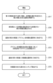
- FIG. 3 is a flowchart showing a film forming method according to the first embodiment.
- FIG. 3 is a process cross-sectional view showing each step of the film forming method according to the first embodiment.
- 7 is a flowchart showing a film forming method according to a second embodiment.
- FIG. 7 is a process cross-sectional view showing a part of the process of the film forming method according to the second embodiment.
- 7 is a flowchart showing a film forming method according to a third embodiment.
- FIG. 7 is a process cross-sectional view showing a part of the process of the film forming method according to the third embodiment.
- FIG. 1 is a schematic diagram showing the overall configuration of an example of a film forming apparatus capable of implementing a film forming method according to an embodiment.
- FIG. 8 is a cross-sectional view showing an example of a graphene-containing film forming module installed in the film forming apparatus of FIG. 7.
- FIG. 9 is a cross-sectional view schematically showing a microwave radiation mechanism in the graphene-containing film deposition module of FIG. 8.
- FIG. 9 is a bottom view schematically showing the top wall portion of the processing container in the graphene-containing film deposition module of FIG. 8.
- FIG. 8 is a cross-sectional view showing an example of a hydrogen-containing plasma processing module installed in the film forming apparatus of FIG. 7.
- FIG. 8 is a cross-sectional view showing an example of a target film deposition module installed in the film deposition apparatus of FIG. 7.
- FIG. FIG. 4 is a diagram showing the results of measuring the contact angles of the surfaces of Samples 1 to 4 of the experimental examples before and after the SiO 2 film formation flow.
- FIG. 1 is a flowchart showing the film forming method according to the first embodiment
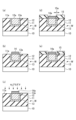
- FIG. 2 is a process cross-sectional view showing each step of the film forming method according to the first embodiment.
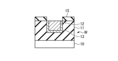
- a substrate W including a first film 11 having a first surface 11a and a second film 12 having a second surface 12a is prepared (step ST1 ).
- the second film 12 is a film different from the first film 11.
- the first film 11 is formed on the base 10 and is, for example, an insulating film (dielectric film).
- a conductive film may be formed between the base 10 and the first film 11.
- the insulating film constituting the first film 11 may be an interlayer insulating film.
- a low dielectric constant (Low-k) film is suitable as the interlayer insulating film.
- the insulating film constituting the first film 11 is not particularly limited, and examples thereof include a SiO 2 film, a SiN film, a SiOC film, a SiON film, and a SiOCN film.
- a recess such as a trench or a hole is formed in the first film 11, and the second film 12 is embedded in the recess.
- the second film 12 is, for example, a conductive film such as a metal film.
- the conductive film (metal film) constituting the second film 12 is not particularly limited, and examples thereof include a Cu film, a Co film, a Ru film, a W film, and a Mo film.
- the combination of the first film 11 and the second film 12 is arbitrary, but for example, the first film 11 is a SiO 2 film and the second film 12 is a Ru film. .
- the substrate W for example, a semiconductor wafer whose base body 10 is made of silicon or a compound semiconductor can be used.
- compound semiconductors include GaAs, SiC, GaN, and InP.
- a barrier film 13 may be provided between the first film 11 and the second film 12.
- the barrier film 13 has a function of suppressing diffusion of metal from the metal film to the insulating film when the first film 11 is an insulating film and the second film 12 is a metal film.
- the barrier film 13 is not particularly limited, but can include a TaN film and a TiN film.
- the barrier film 13 has a third surface 13a formed between the first surface 11a and the second surface 12a.
- the substrate W is not limited to the structure shown in FIG. 2A as long as it has a first film having an exposed first surface and a second film having an exposed second surface.
- a graphene-containing film 14 is selectively formed on the second surface 12a of the substrate W (step ST2).
- the graphene-containing film 14 is a carbon material film mainly containing graphene, which is configured as an aggregate of a six-membered ring structure by covalent bonds (sp 2 bonds) of carbon atoms, and is used to form a target film to be formed next. Formed as a film that inhibits (blocks)
- the graphene-containing film 14 may be formed only of graphene, or may contain other carbon materials such as graphite, diamond, charcoal, carbon nanotubes, fullerene, or an amorphous component in addition to graphene. It only needs to be composed of at least 50% graphene, preferably 90% or more. In general, graphene deposition can be selective on metals over insulators. Therefore, when the second film 12 is a metal film, the graphene-containing film 14 is selectively formed on the second surface 12a of the second film 12.
- the graphene-containing film 14 can be formed by plasma CVD.
- the plasma ALD method may also be used.
- a carbon-containing gas can be used as a raw material gas during film formation.
- H 2 gas or N 2 gas may be added.
- a rare gas such as Ar, He, Ne, Kr, or Xe may be added as a plasma generating gas or the like.
- carbon-containing gases examples include ethylene (C 2 H 4 ), methane (CH 4 ), ethane (C 2 H 6 ), propane (C 3 H 8 ), propylene (C 3 H 6 ), and acetylene (C 2 H 6 ). Hydrocarbon gases such as 2 ) can be used.
- the plasma used to form the graphene-containing film 14 is not particularly limited, and various types can be used, such as capacitively coupled plasma, inductively coupled plasma, and microwave plasma. Among these, microwave plasma can be preferably used. Microwave plasma is a plasma with high radical density and low electron temperature. Therefore, the carbon-containing gas can be dissociated into a state suitable for graphene growth at a relatively low temperature, and a high-quality film can be obtained. Further, the graphene-containing film 14 can be formed on the second film 12 without damaging the second film 12 as the base or the film being formed.
- the pressure when forming the graphene-containing film 14 can be appropriately set depending on the plasma to be generated.
- the temperature at which the graphene-containing film 14 is formed may be 250 to 450°C, preferably 400 to 450°C. If it is lower than 250°C, the effect of inhibiting the formation of the target film (blocking property) will tend to be low even in the next plasma treatment, and if it exceeds 450°C, if the second film 12 is a metal film, There is a concern that the film 12 may be damaged.
- the thickness of the graphene-containing film 14 may be in the range of 0.5 to 10 nm, preferably in the range of 4 to 6 nm. If it is thinner than 0.5 nm, it will be difficult to obtain the effect of inhibiting the formation of the target film even in the next plasma treatment, and there is a fear that the second film 12 will be damaged by the next plasma treatment. On the other hand, if the film thickness exceeds 10 nm, a relatively large amount of carbon nanowires, carbon nanowalls, etc. may be formed, and an unintended graphene-containing film may be formed, and as a result, the effect of inhibiting film formation may be reduced. There is sex.
- step ST3 the substrate W on which the graphene-containing film 14 has been formed is subjected to a process using hydrogen-containing plasma (step ST3).
- the treatment with hydrogen-containing plasma is a modification treatment for increasing the effect of inhibiting the formation of the target film of the graphene-containing film 14.
- the use of graphene as a film formation inhibitor for a target film is described in Patent Documents 3 and 4 mentioned above. However, it has been found that simply forming graphene does not provide a sufficient effect of inhibiting the formation of the target film. This is because if graphene is simply formed, the defects existing on the surface of graphene will become the starting point for nucleation of the target film, and the formation of the target film will proceed from the generated nucleus of the target film. Conceivable.
- the graphene-containing film 14 can be modified into a film that has a high film-forming inhibiting effect on the target film, resulting in a modified graphene-containing film 14a.
- Hydrogen-containing plasma can be formed by turning hydrogen-containing gas into plasma.
- Hydrogen gas H 2 gas
- H 2 gas can be used as the hydrogen-containing gas.
- NH 3 gas, H 2 O gas, H 2 O 2 gas, HF gas, etc. can be used.
- hydrogen also includes deuterium, and the hydrogen-containing gas may be deuterium gas (D 2 gas) or heavy water (D 2 O).
- an inert gas for example, a rare gas such as Ar gas or N 2 gas
- the plasma used in the hydrogen-containing plasma treatment is not particularly limited, and various types can be used, such as capacitively coupled plasma, inductively coupled plasma, and microwave plasma.
- Microwave plasma is a plasma with high radical density and low electron temperature, so it can perform processing efficiently with low damage.
- the hydrogen-containing plasma treatment in step ST3 may be performed in a different processing container or in the same processing container as the film-forming treatment for the graphene-containing film 14 in step ST2.
- the hydrogen-containing plasma treatment in step ST3 can be performed in the same processing container as the deposition treatment of the graphene-containing film 14 in step ST2.
- the hydrogen-containing plasma treatment in step ST3 can be performed, for example, at a temperature of 100 to 400° C., a power of 50 to 3000 W, and a time of 1 to 60 sec. Further, the pressure when performing the hydrogen-containing plasma treatment can be appropriately set depending on the plasma to be generated.
- the target film 15 is selectively formed on the first surface 11a of the substrate W (step ST4).
- the target film 15 is not particularly limited, but may be, for example, a SiO 2 film. Formation of the SiO 2 film includes a step of coating the first surface 11a with a metal-containing catalyst layer, and a step of exposing the coated substrate W to a processing gas containing silanol gas, as described in Patent Document 3. This can be suitably carried out by a process having the following steps.
- the step of coating the first surface 11a of the first film 11 with a metal-containing catalyst layer can be performed by exposing the substrate W to a metal-containing gas.
- gas containing metal can be selectively adsorbed to the first surface 11a
- a metal-containing catalyst layer can be selectively formed on 11a. Metals react to form chemisorbed layers less than a monolayer thick.
- Each gas pulse includes a respective purge or evacuation step to remove residual gas from the processing vessel.
- modified graphene-containing membrane has low reactivity, metal-containing catalysts are difficult to adsorb, and a metal-containing catalyst layer is selectively formed on the first surface 11a of the first membrane 11, as described below.
- the silanol gas selectively reacts with the metal-containing catalyst layer on the first surface 11a.
- the metal for forming the metal-containing catalyst layer one or both of Al and Ti can be used.
- the metal-containing catalyst layer include metal Al, Al 2 O 3 , AlN, Al alloy, Al-containing precursor, metal Ti, TiO 2 , TiN, Ti alloy, Ti-containing precursor, TiAlN, TiAlC, etc. I can do it.
- Various types of Al-containing precursors can be used, such as organic Al compounds such as AlMe 3 (TMA).
- TMA organic Al compounds
- Ti-containing precursors such as organic Ti compounds such as Ti(NEt 2 ) 4 (TDEAT).
- silanol gas for example, tris(tert-pentoxy)silanol (TPSOL), tris(tert-butoxy)silanol, and bis(tert-butoxy)(isopropoxy)silanol can be used.
- the processing gas may contain an inert gas such as Ar gas in addition to silanol gas.
- the thickness of the SiO2 film is controlled by the self-limiting adsorption of silanol gas onto the metal-containing catalyst layer.
- the catalytic action of the metal-containing catalyst layer continues until the film thickness reaches about 3 to 5 nm.
- the process of coating the metal-containing catalyst layer and the process of exposing the process gas containing silanol are repeated once or multiple times to selectively form a SiO 2 film with a desired thickness on the first surface 11a.
- the SiO 2 film can be formed at a temperature of 150° C. or lower, preferably 120° C. or lower, and even 100° C. without using plasma.
- the SiO 2 film may be formed by general CVD or ALD as long as selective film formation is possible.
- the target film 15 may be, for example, an Al 2 O 3 film, a SiN film, a ZrO 2 film, a HfO 2 film, etc. in addition to the SiO 2 film. These can also be selectively formed on the first surface 11a of the first film 11 by CVD, ALD, or the like.
- step ST5 the excess portion of the target film 15 is removed by etching, if necessary.
- the target film 15 is also formed on the third surface 13a of the barrier film 13, and the end of the target film 15 protrudes from the first surface 11a.
- This protruding portion 15a becomes an extra portion.
- the target film 15 is formed thicker than the desired thickness in the film thickness direction, there is an extra portion in the thickness direction as well.
- the protruding portion 15a of the target film 15 and the portion thicker than the desired thickness are removed by etching as redundant portions.
- Etching at this time is not particularly limited and can be performed by various methods.
- gas etching using HF gas and TMA gas or gas etching using HF gas and NH 3 gas can be performed without plasma.
- Gas etching using HF gas and TMA gas repeats the steps of supplying HF gas to the surface of the SiO 2 film to fluorinate the surface, and then supplying TMA gas to remove the fluoride by ligand exchange. This can be done by ALE.
- gas etching using HF gas and NH 3 gas is known as chemical oxide removal (COR).
- HF gas and NH 3 gas are adsorbed on the surface of the SiO 2 film, and these are reacted with the oxide film to produce ammonium fluorosilicate (AFS), which is an ammonium fluoride-based compound, and this is heated. This is done by removing.
- AFS ammonium fluorosilicate
- the material of the target film 15 is not limited, and conventionally commonly performed H 2 plasma treatment or plasma etching using CF-based gas can also be used.
- step ST5 is not essential, and the target film 15 may If there is little risk of protruding from the surface 11a of the film 1 and the thickness of the target film 15 is a desired thickness, it is not necessary to perform this step.
- the target film 15 can be selectively formed only on the first surface 11a of the first film 11.
- step ST3 and step ST4 may be performed repeatedly. This is effective when the film formation inhibiting effect of the graphene-containing film weakens while forming the target film 15 in step ST4.
- the conditions for implementing the hydrogen-containing plasma treatment in step ST3 may be different between the first and second and subsequent times, or may be the same.
- Non-Patent Document 1 when using SAM as a film formation inhibitor that inhibits the formation of a target film, multiple steps such as oxidation treatment and plasma treatment are performed. have. For this reason, a plurality of treatments including heating are performed on the metal surface of the second film. Since the SAM itself is a molecular adsorption layer and has a film thickness of about 1 nm at most, damage to the metal film is likely to occur when the metal surface of the second film is subjected to multiple treatments. Further, since the SAM has a film thickness of about 1 nm, even if the film is selectively formed, lateral growth may not be suppressed. Furthermore, when the second film is a Ru film, it is difficult to inhibit film formation by SAM.
- the target film 15 can be selectively formed on the first surface 11a of the first film 11 with higher precision while suppressing damage.
- FIG. 3 is a flowchart showing a film forming method according to the second embodiment
- FIG. 4 is a process sectional view showing a part of the steps of the film forming method according to the second embodiment.
- a pretreatment step is added to the film forming method described in the first embodiment.
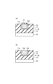
- the second film 12 is made of metal in the substrate W having the structure shown in FIG. 2(a)
- the substrate W is held in the atmosphere, as shown in FIG. A natural oxide film 16 may be formed in some cases.
- the second surface 12a for forming the graphene-containing film 14 is not exposed, it is necessary to remove the natural oxide film 16 prior to forming the graphene-containing film 14 in step ST2. .
- a first film 11 having a first surface 11a and a second film 12 having a natural oxide film 16 formed on its surface are formed.
- a substrate W including the following is prepared (step ST1').
- a process of reducing and removing the natural oxide film 16 is performed as a pretreatment to expose the second surface 12a of the second film 12 (step ST6).
- This step ST6 can be performed, for example, by hydrogen annealing or hydrogen plasma treatment.
- the temperature at this time can be 500°C or less.
- Hydrogen plasma treatment can be performed at a lower temperature than hydrogen annealing.
- Hydrogen annealing is performed by introducing hydrogen gas (H 2 gas) into the processing container while heating the substrate W within the processing container.
- hydrogen plasma processing hydrogen plasma is applied to the substrate W in the processing container. All of these may be performed using H 2 gas alone, or may be performed by adding an inert gas such as Ar gas to H 2 gas.
- step ST2 is a step of selectively forming the graphene-containing film 14
- step ST3 is a step of performing treatment with hydrogen-containing plasma
- step ST4 is a step of selectively forming a target film. Then, if necessary, the etching process of step ST5 is performed.
- FIG. 5 is a flowchart showing a film forming method according to the second embodiment
- FIG. 6 is a process cross-sectional view showing a part of the process of FIG.
- step ST7 is a process that is performed when necessary due to the device.
- step ST7 may be performed after steps ST1' to ST5 are performed.
- This step ST7 can be performed, for example, by hydrogen plasma treatment.
- the temperature at this time can be 500°C or less.
- Hydrogen plasma processing is performed by applying hydrogen plasma to a substrate W placed in a processing container.
- the hydrogen plasma treatment may be performed using H 2 gas alone, or may be performed by adding an inert gas such as Ar gas to H 2 gas.
- FIG. 7 is a schematic diagram showing the overall configuration of an example of a film forming apparatus that can carry out the film forming method according to an embodiment.
- the film forming apparatus 100 in FIG. 7 is a multi-chamber type apparatus capable of implementing the film forming method according to the first embodiment, and is configured as an apparatus capable of performing steps ST2 to ST5 in-situ. Ru.
- the film forming apparatus 100 includes a graphene-containing film forming module 200, a hydrogen-containing plasma processing module 300, a target film forming module 400, and an etching module 500. These modules are connected to the vacuum transfer chamber 101 via gate valves G, respectively.
- the inside of the vacuum transfer chamber 101 is evacuated by a vacuum pump and maintained at a predetermined degree of vacuum.
- the graphene-containing film forming module 200 selectively forms a graphene-containing film on the second surface of the substrate W by plasma CVD or plasma ALD.
- the hydrogen-containing plasma processing module 300 is for treating the substrate W on which a graphene-containing film has been formed with hydrogen-containing plasma to modify the graphene-containing film.
- the target film deposition module 400 selectively forms a target film, for example, a SiO 2 film, on the first surface of the substrate W.
- the etching module 500 is for etching away the excess portion of the target film.
- Three load lock chambers 102 are connected to the other three walls of the vacuum transfer chamber 101 via gate valves G1.
- An atmospheric transfer chamber 103 is provided on the opposite side of the vacuum transfer chamber 101 with the load lock chamber 102 in between.
- the three load lock chambers 102 are connected to an atmospheric transfer chamber 103 via a gate valve G2.
- the load lock chamber 102 controls the pressure between atmospheric pressure and vacuum when the substrate W is transferred between the atmospheric transfer chamber 103 and the vacuum transfer chamber 101.
- a wall portion of the atmospheric transfer chamber 103 opposite to the wall portion to which the load lock chamber 102 is attached has three carrier attachment ports 105 for attaching carriers (such as FOUPs) C for accommodating the substrates W. Further, an alignment chamber 104 for aligning the substrate W is provided on a side wall of the atmospheric transfer chamber 103. A downflow of clean air is formed in the atmospheric transfer chamber 103.
- carriers such as FOUPs
- a first transport mechanism 106 is provided within the vacuum transport chamber 101.
- the first transport mechanism 106 transports the substrate W to the graphene-containing film deposition module 200, the hydrogen-containing plasma processing module 300, the target film deposition module 400, the etching module 500, and the load lock chamber 102.
- the first transport mechanism 106 has two independently movable transport arms 107a and 107b.
- a second transport mechanism 108 is provided within the atmospheric transport chamber 103.
- the second transport mechanism 108 transports the substrate W to the carrier C, the load lock chamber 102, and the alignment chamber 104.
- the film forming apparatus 100 has an overall control section 110.
- the overall control section 110 includes a main control section having a CPU (computer), an input device, an output device, a display device, and a storage device.
- the main control unit controls each component of the graphene-containing film deposition module 200, the hydrogen-containing plasma processing module 300, the target film deposition module 400, the etching module 500, the vacuum transfer chamber 101, and the load-lock chamber 102.
- the main control unit of the overall control unit 110 causes the film forming apparatus 100 to perform film formation, for example, based on a processing recipe stored in a storage medium built into the storage device or a storage medium set in the storage device. Execute the action for the purpose.
- each module may be provided with a lower-level control section, and the overall control section 110 may be configured as a higher-level control section.
- the substrate W is taken out from the carrier C connected to the atmospheric transport chamber 103 by the second transport mechanism 108, passes through the alignment chamber 104, and then is placed in one of the load locks. It is carried into the room 102.
- the first transport mechanism 106 transfers the substrate W to the graphene-containing film deposition module 200, the hydrogen-containing plasma processing module 300, the target film deposition module 400, and the etching module. 500, and the processes of steps ST2 to ST5 described above are performed.
- the first transport mechanism 106 transports the substrate W to one of the load lock chambers 102, and the second transport mechanism 108 returns the substrate W in the load lock chamber 102 to the carrier C.
- the above-described processing is performed continuously and simultaneously on a plurality of substrates W, and the film formation processing on a predetermined number of substrates W is completed.
- the film forming apparatus 100 performs the processes of steps ST2 to ST5 in separate single-wafer modules, so it is easy to set the optimum temperature for each process, and a series of processes can be performed without breaking the vacuum. Therefore, oxidation during the treatment process can be suppressed.
- steps ST2 to ST5 are performed in separate modules, but two or more steps may be performed in the same module.
- steps ST6 and the graphene-containing film removal process in step ST7 the size of the vacuum transfer chamber 101 is changed and a pretreatment module and a graphene-containing film removal module are installed in the vacuum transfer chamber 101.
- these processes may be performed by other modules.
- the film forming apparatus is not limited to the form shown in FIG. 7, and the connection form of each module to the vacuum transfer chamber is arbitrary. It may also be a form in which each module is transported serially.
- FIG. 8 is a cross-sectional view schematically showing an example of a graphene-containing film forming module
- FIG. 9 is a cross-sectional view schematically showing a microwave radiation mechanism in the graphene-containing film forming module of FIG. 8
- FIG. 2 is a bottom view schematically showing a top wall portion of a processing container in a graphene-containing film deposition module.
- This graphene-containing film deposition module 200 is configured as a microwave plasma processing apparatus, and includes a processing container 201, a mounting table 202, a gas supply section 203, an exhaust device 204, and a microwave introduction device 205. .
- the processing container 201 accommodates the substrate W, and is made of a metal material such as aluminum (Al) and its alloy, and has a substantially cylindrical shape, and includes a plate-shaped top wall portion 211 and a bottom wall portion 213. and a side wall portion 212 that connects these.
- the inner surfaces of the top wall portion 211 and the side wall portion 212 constitute the inner wall of the processing container 201 .
- the inner wall surface of the processing container 201 may be coated with Al2O3 , Y2O3 , or the like.
- the microwave introduction device 205 is provided at the top of the processing container 201 and functions as a plasma generation means that introduces electromagnetic waves (microwaves) into the processing container 201 to generate plasma.
- the microwave introducing device 205 will be explained in detail later.
- the ceiling wall portion 211 has a plurality of openings into which a microwave radiation mechanism and a gas introduction nozzle, which will be described later, of the microwave introduction device 205 are fitted.
- the side wall portion 212 has a loading/unloading port 214 for loading/unloading the substrate W into/from the vacuum transfer chamber 101 adjacent to the processing container 201 .
- the loading/unloading port 214 is opened and closed by a gate valve G.
- An exhaust device 204 is provided on the bottom wall portion 213.
- the exhaust device 204 is provided in an exhaust pipe 216 connected to the bottom wall portion 213, and includes a vacuum pump and a pressure control valve.
- the inside of the processing container 201 is evacuated via the exhaust pipe 216 by the vacuum pump of the exhaust device 204 .
- the pressure within the processing container 201 is controlled by a pressure control valve.
- the mounting table 202 is arranged inside the processing container 201, and the substrate W is mounted thereon.
- the mounting table 202 has a disk shape and is made of ceramics such as AlN, for example.
- the mounting table 202 is supported by a cylindrical support member 220 extending upward from the center of the bottom of the processing container 201 .
- a support plate 221 is provided between the bottom wall portion 213 of the processing container 201 and the support member 220.
- the support member 220 and the support plate 221 are made of ceramics such as AlN.
- a guide ring 281 for guiding the substrate W is provided at the outer edge of the mounting table 202.
- a lifting pin (not shown) for raising and lowering the substrate W is provided so as to be projectable and retractable from the upper surface of the mounting table 202.
- a resistance heating type heater 282 is embedded inside the mounting table 202, and this heater 282 heats the substrate W thereon via the mounting table 202 by being supplied with power from a heater power source 283.
- a thermocouple (not shown) is inserted into the mounting table 202, and the heating temperature of the substrate W can be controlled based on a signal from the thermocouple.
- an electrode 284 having the same size as the substrate W is buried above the heater 282 in the mounting table 202, and a high frequency bias power source 222 is electrically connected to the electrode 284.
- a high frequency bias for drawing ions is applied to the mounting table 202 from the high frequency bias power supply 222. Note that the high frequency bias power supply 222 may not be provided depending on the characteristics of plasma processing.
- the gas supply unit 203 supplies a plasma generating gas (rare gas such as Ar gas), a carbon-containing gas for forming a graphene film (for example, ethylene (C 2 H 4 ), methane (CH 4 ), ethane (C 2 H 6 ) ), propane (C 3 H 8 ), propylene (C 3 H 6 ), acetylene (C 2 H 2 ), and other hydrocarbon gases) into the processing container 201 .
- a plasma generating gas ultraviolet gas
- a carbon-containing gas for forming a graphene film for example, ethylene (C 2 H 4 ), methane (CH 4 ), ethane (C 2 H 6 ) ), propane (C 3 H 8 ), propylene (C 3 H 6 ), acetylene (C 2 H 2 ), and other hydrocarbon gases
- H 2 gas or N 2 gas may be supplied.
- the gas supply unit 203 includes a gas supply mechanism 292 having a plurality of gas supply sources for supplying these gases,
- the gas supply unit 203 further includes a common pipe 291 that guides gas from the gas supply mechanism 292 and a plurality of gas introduction nozzles 223 connected to the pipe 291.
- the gas introduction nozzle 223 is fitted into an opening formed in the top wall 211 of the processing container 201, and gas from the gas supply mechanism 292 is introduced into the processing container 201 via the piping 291 and the gas introduction nozzle 223. be done.
- the dissociation of the gas may be adjusted by adjusting the distance from the substrate W to the gas introduction position using appropriate means.
- the microwave introduction device 205 is provided above the processing container 201 and functions as a plasma generation means that introduces electromagnetic waves (microwaves) into the processing container 201 to generate plasma.
- the microwave introduction device 205 includes a ceiling wall portion 211 functioning as a top plate, a microwave output portion 230, and an antenna unit 240.
- the microwave output unit 230 generates microwaves, distributes the microwaves to a plurality of paths, and outputs the microwaves, and includes a microwave power source, a microwave oscillator, an amplifier, and a distributor.
- the microwave oscillator is solid state, and oscillates microwaves (for example, PLL oscillation) at, for example, 860 MHz.
- the frequency of the microwave is not limited to 860 MHz, and may be in the range of 700 MHz to 10 GHz, such as 2.45 GHz, 8.35 GHz, 5.8 GHz, and 1.98 GHz.
- Microwaves oscillated by a microwave oscillator are amplified by an amplifier and distributed to a plurality of paths by a distributor.
- the distributor distributes microwaves while matching the impedance between the input side and the output side.
- the antenna unit 240 introduces the microwave output from the microwave output section 230 into the processing container 201.
- Antenna unit 240 includes a plurality of antenna modules 241. Each of the plurality of antenna modules 241 introduces the microwaves distributed by the distributor into the processing container 201.
- the plurality of antenna modules 241 include an amplifier section 242 that mainly amplifies and outputs distributed microwaves, and a microwave radiation mechanism 243 that radiates the microwaves output from the amplifier section 242 into the processing container 201. .
- the amplifier section 242 includes a phase shifter, a variable gain amplifier, a main amplifier, and an isolator, which are arranged in order from the upstream side. After the phase of the microwave is adjusted by the phase shifter and the power level of the microwave is adjusted by the variable gain amplifier, the microwave is amplified by the main amplifier.
- the main amplifier is configured as a solid state amplifier.
- the isolator separates reflected microwaves that are reflected by an antenna section of a microwave radiation mechanism 243 and directed toward the main amplifier, which will be described later.
- a plurality of microwave radiation mechanisms 243 are provided on the ceiling wall portion 211. Further, the microwave radiation mechanism 243 includes a coaxial tube 251, a power feeding section 255, a tuner 254, and an antenna section 256, as shown in FIG.
- the coaxial tube 251 has a cylindrical outer conductor 252, an inner conductor 253 provided coaxially with the outer conductor 252 within the outer conductor 252, and a microwave transmission path between them.
- the power feeding section 255 feeds the amplified microwave from the amplifier section 242 to the microwave transmission line.
- Microwaves amplified by the amplifier section 242 are introduced into the power feeding section 255 from the side of the upper end of the outer conductor 252 via a coaxial cable.
- the microwave power is fed to a microwave transmission path between the outer conductor 252 and the inner conductor 253, and the microwave power propagates toward the antenna section 256.
- the antenna section 256 radiates microwaves from the coaxial tube 251 into the processing container 201, and is provided at the lower end of the coaxial tube 251.
- the antenna section 256 includes a disk-shaped planar antenna 261 connected to the lower end of the inner conductor 253, a slow-wave material 262 placed on the top side of the planar antenna 261, and a slow wave material 262 placed on the bottom side of the planar antenna 261. and a microwave transmitting plate 263.
- the microwave transmitting plate 263 is fitted into the top wall portion 211, and its lower surface is exposed to the internal space of the processing container 201.
- the planar antenna 261 has a slot 261a formed to penetrate therethrough. The shape of the slot 261a is appropriately set so that microwaves are efficiently radiated.
- a dielectric material may be inserted into the slot 261a.
- the slow-wave material 262 is made of a material with a dielectric constant greater than that of vacuum, and its thickness allows the phase of the microwave to be adjusted so that the radiated energy of the microwave is maximized. can.
- the microwave transmission plate 263 is also made of a dielectric material and has a shape that allows microwaves to be efficiently radiated in the TE mode. The microwaves transmitted through the microwave transmission plate 263 generate plasma in the space inside the processing container 201 .
- the material constituting the slow wave material 262 and the microwave transmission plate 263 for example, quartz, ceramics, fluororesin such as polytetrafluoroethylene resin, polyimide resin, etc. can be used.
- the tuner 254 matches the impedance of the load to the characteristic impedance of the microwave power source in the microwave output section 230.
- Tuner 254 constitutes a slug tuner.
- the tuner 254 includes two slugs 271a and 271b, an actuator 272 that independently drives these two slugs, and a tuner controller 273 that controls the actuator 272.
- the slugs 271a and 271b are arranged at a portion of the coaxial tube 251 closer to the base end (upper end) than the antenna section 256.
- the slugs 271a and 271b are plate-shaped and ring-shaped, are made of a dielectric material such as ceramics, and are arranged between the outer conductor 252 and the inner conductor 253 of the coaxial tube 251. Further, as the actuator 272, for example, one having two screws provided inside the inner conductor 253 and into which the slugs 271a and 271b are screwed together, and a motor that rotates these screws can be used. . For example, the slugs 271a and 271b are individually driven by rotating screws using a motor.
- the actuator 272 moves the slugs 271a, 271b in the vertical direction based on a command from the tuner controller 273, and adjusts the positions of the slugs 271a, 271b so that the impedance at the terminal end becomes 50 ⁇ .
- the main amplifier of the amplifier section 242, the tuner 254, and the planar antenna 261 are arranged close to each other.
- the tuner 254 and the planar antenna 261 constitute a lumped constant circuit and function as a resonator.
- the tuner 254 directly tunes the plasma load, it is possible to tune the plasma with high accuracy. Therefore, the influence of reflection on the planar antenna 261 can be eliminated.
- the corresponding microwave transmission plates 263 are evenly arranged in a hexagonal close-packed arrangement. That is, one of the seven microwave transmitting plates 263 is arranged at the center of the ceiling wall portion 211, and the other six microwave transmitting plates 263 are arranged around it. These seven microwave transmitting plates 263 are arranged so that adjacent microwave transmitting plates are equally spaced. Further, the plurality of nozzles 223 of the gas supply mechanism 203 are arranged so as to surround the central microwave transmission plate. Note that the number of microwave radiation mechanisms 243 is not limited to seven.
- the substrate W is carried into the processing chamber 201 and placed on the mounting table 202.
- the pressure inside the processing chamber 201 is controlled, and a graphene-containing film is formed by, for example, microwave plasma CVD.
- Ar gas which is a plasma generation gas
- Ar gas is supplied from the gas introduction nozzle 223 directly below the top wall portion 211 of the processing chamber 201 .
- the microwaves distributed and outputted from the microwave output section 230 of the microwave introduction device 205 are radiated into the processing container 201 through the plurality of antenna modules 241 of the antenna unit 240, and the plasma is ignited. .
- each antenna module 241 the microwave is individually amplified by the main amplifier of the amplifier section 242, and is fed to each microwave radiation mechanism 243.
- the microwave fed to the microwave radiation mechanism 243 is transmitted through the coaxial tube 251 and reaches the antenna section 256.
- the impedance of the microwave is automatically matched by the slug 271a and the slug 271b of the tuner 254, and the microwave is transmitted from the tuner 254 to the planar antenna 261 via the slow wave material 262 of the antenna section 256 with substantially no power reflection. It is radiated from the slot 261a.
- the wave is further transmitted through the microwave transmission plate 263 and transmitted through the surface (lower surface) of the microwave transmission plate 263 that is in contact with the plasma, forming a surface wave, and a surface wave plasma caused by Ar gas is generated in the area directly under the ceiling wall portion 211. generated.
- a carbon-containing gas such as C 2 H 4 gas, which is a film-forming raw material gas, is supplied from the gas introduction nozzle 223 .
- N 2 gas or H 2 gas may be supplied as necessary.
- the substrate W is disposed in a region apart from the plasma generation region, and the plasma diffused from the plasma generation region is supplied to the substrate W, so that plasma with a low electron temperature forms on the substrate W, resulting in low damage. , and becomes a high-density plasma consisting mainly of radicals. Therefore, nucleation and creeping growth proceed favorably, and graphene crystals with fewer defects grow. As a result, a graphene-containing film of good quality is formed, which can become a film that inhibits the formation of the target film.
- the substrate temperature when forming the graphene-containing film may be 250 to 450° C., and the film thickness may be 0.5 to 10 nm.
- C 2 H 4 gas as a carbon-containing gas was supplied to the plasma generation region to cause dissociation, but dissociation may also be suppressed by dissociation by plasma diffused from the plasma generation region by appropriate means. good.
- the plasma may be directly ignited by supplying a carbon-containing gas such as C 2 H 4 gas to the plasma generation region without using Ar gas as the plasma generation gas.
- microwaves distributed into a plurality of parts are individually amplified by the amplifier section 242 and individually radiated from the microwave radiation mechanism 243 to generate microwave plasma. It is compact and eliminates the need for isolators and combiners. Furthermore, since the tuner 254 can perform highly accurate tuning including the plasma at the planar slot antenna attachment part where impedance mismatch exists, it is possible to reliably eliminate the influence of reflection and perform highly accurate plasma control. Furthermore, by providing a plurality of microwave transmission plates 263 in this manner, the total area of the microwave transmission region is made smaller than when the microwave plasma source has a single microwave transmission path and microwave transmission plate. be able to. Thereby, the power of the microwave required to stably ignite and discharge plasma can be reduced.
- the graphene-containing film formation module is not limited to the microwave plasma processing apparatus as in this example, but may be one that uses other plasmas, such as a capacitively coupled plasma processing apparatus or an inductively coupled plasma processing apparatus.
- FIG. 11 is a cross-sectional view schematically showing an example of a hydrogen-containing plasma processing module.
- This hydrogen-containing plasma processing module 300 has a substantially cylindrical metal processing container 301.
- An exhaust pipe 311 is connected to the bottom of the processing container 301, and the exhaust pipe 311 includes an automatic pressure control valve for controlling the pressure inside the processing container 301 and a vacuum pump for evacuating the inside of the processing container 301.
- An exhaust mechanism 312 is provided. This exhaust mechanism 312 allows the inside of the processing container 301 to be evacuated and controlled to a desired pressure.
- a loading/unloading port 313 for loading/unloading the substrate W between the processing container 301 and the vacuum transfer chamber 101 provided adjacent to the processing container 301, and a gate valve G for opening/closing the loading/unloading port 313. and is provided.
- a mounting table 302 for horizontally supporting the substrate W is provided inside the processing container 301.
- the mounting table 302 is supported at the center of the bottom wall of the processing container 301 via a support member 303.
- the mounting table 302 is grounded via the processing container 301 and functions as a lower electrode.
- the mounting table 302 may be made of metal or ceramics, and if it is made of ceramics, an electrode plate is provided therein.
- a heater 318 for heating the substrate W is provided inside the mounting table 302.
- a plurality of lifting pins (not shown) for supporting and raising and lowering the substrate W are provided on the mounting table 302 so as to be projectable and retractable with respect to the surface of the mounting table 302.
- a circular hole is formed in the top wall 301a of the processing container 301, and a disk-shaped shower head 320 functioning as an upper electrode is fitted into the hole via an insulating member 326.
- the shower head 320 includes a base member 321 and a shower plate 322.
- a gas diffusion space 323 is formed between the base member 321 and the shower plate 322.
- a plurality of gas discharge holes 324 are formed in the shower plate 322 and penetrate from the gas diffusion space 323 into the processing container 301 .
- a gas introduction hole 325 is formed in the center of the base member 321 so as to penetrate into the gas diffusion space 323.
- a pipe 331 extending from a gas supply section 330 is connected to the gas introduction hole 325, so that gas from the gas supply section 330 is discharged into the processing container 301 via the shower head 320.
- the gas supply unit 330 supplies hydrogen-containing gas such as H2 gas.
- a rare gas such as Ar gas or an inert gas such as N 2 gas may be supplied.
- As the hydrogen-containing gas in addition to H 2 gas, NH 3 gas, H 2 O gas, H 2 O 2 gas, HF gas, etc. can be used.
- a high frequency power source 316 is connected to the shower head 320 which functions as an upper electrode through a power supply line 317.
- a matching box 315 is connected in the middle of the power supply line 317 .
- the substrate W on which a graphene-containing film has been formed is carried into the processing chamber 301 and placed on the mounting table 302.
- the pressure inside the processing container 301 is controlled, and a hydrogen-containing gas such as H 2 gas and an inert gas as necessary are supplied from the gas supply unit 330 to the shower head 320. It is supplied into the processing container 301 through the. Then, with the gas being supplied, high frequency power is applied from the high frequency power source 316 to the shower head 320 to generate hydrogen-containing plasma between the shower head 320 and the mounting table 302. As a result, the substrate W is subjected to hydrogen-containing plasma treatment.
- a hydrogen-containing gas such as H 2 gas and an inert gas as necessary
- the graphene-containing film formed on the substrate W can be modified into a film that is highly effective in inhibiting the formation of the target film.
- microwave plasma is a plasma with high radical density and low electron temperature, so it can perform processing efficiently with low damage.
- a module having the same configuration as the graphene-containing film deposition module 200 described above can be used.
- the graphene-containing film deposition module 200 has the function of the hydrogen-containing plasma processing module 300, and after forming the graphene-containing film, the hydrogen-containing plasma is continuously applied in the same processing container. Processing may be performed.
- FIG. 12 is a cross-sectional view schematically showing an example of a target film deposition module.
- This target film deposition module 400 has a substantially cylindrical processing container 401 that is configured in an airtight manner. It is supported by a cylindrical support member 403 provided at the center of the bottom wall.
- a heater 405 for heating the substrate W is provided on the mounting table 402.
- the mounting table 402 is provided with a plurality of lifting pins (not shown) for supporting and raising and lowering the substrate W so as to be projectable and retractable with respect to the surface of the mounting table 402.
- a shower head 410 is provided on the ceiling wall of the processing container 401 so as to face the mounting table 402 for introducing a processing gas into the processing container 401 into the processing container 401 in the form of a shower.
- the shower head 410 is for discharging gas supplied from a gas supply section 430 (described later) into the processing container 401, and has a gas inlet 411 formed in its upper part for introducing the gas. Further, a gas diffusion space 412 is formed inside the shower head 410, and a large number of gas discharge holes 413 communicating with the gas diffusion space 412 are formed on the bottom surface of the shower head 410.
- An exhaust chamber 421 that protrudes downward is provided on the bottom wall of the processing container 401.
- An exhaust pipe 422 is connected to the side surface of the exhaust chamber 421, and an exhaust device 423 having a vacuum pump, a pressure control valve, etc. is connected to the exhaust pipe 422.
- an exhaust device 423 having a vacuum pump, a pressure control valve, etc. is connected to the exhaust pipe 422.
- a loading/unloading port 427 for loading/unloading the substrate W to/from the vacuum transfer chamber 101 is provided on the side wall of the processing container 401, and the loading/unloading port 427 is opened and closed by a gate valve G.
- the gas supply section 430 supplies gas necessary for forming the target film.
- a gas containing a metal for forming a metal-containing catalyst layer and a processing gas containing silanol are supplied.
- an inert gas such as Ar gas may be supplied.
- the metal for forming the metal-containing catalyst layer one or both of Al and Ti can be used.
- an organic Al compound such as AlMe 3 (TMA) can be used as an Al precursor.
- TMA AlMe 3
- the gate valve G is opened, the substrate W is carried into the processing chamber 401 from the carry-in/out port 427, and placed on the mounting table 402.
- the mounting table 402 is heated to a predetermined temperature by a heater 405, and the substrate W placed on the mounting table 402 is heated to that temperature.
- the inside of the processing container 401 is evacuated by the vacuum pump of the exhaust device 423, and the pressure inside the processing container 401 is adjusted to a predetermined pressure.
- TMA gas is supplied as a metal-containing gas from the gas supply unit 430 to selectively form a metal-containing catalyst layer on the first surface of the substrate W.
- a processing gas containing silanol is supplied onto the metal-containing catalyst layer.
- the step of coating the metal-containing catalyst layer and the step of supplying the silanol-containing processing gas are repeated once or multiple times to selectively coat the first surface of the substrate W with a desired thickness of SiO 2 .
- the SiO 2 film can be formed at a temperature of 150° C. or lower, preferably 120° C. or lower, and even 100° C. without using plasma.
- the target film may be formed by CVD or ALD, and in that case as well, a module having the same configuration as the target film deposition module 400 can be used.
- the etching module 500 is for removing the excess portion of the target film formed on the first surface of the substrate W, and when the target film 15 is a SiO 2 film, the etching module 500 It can be performed without plasma using gas etching using HF gas and TMA gas, or gas etching using HF gas and NH 3 gas. In this case, a module having the same configuration as the target film deposition module 400 described above can be used.
- the etching can be performed using H 2 plasma processing or plasma etching using CF-based gas, which has been commonly performed in the past.
- the same configuration as the hydrogen-containing plasma processing module 300 described above may be used. It is possible to use a module capable of generating plasma having the following characteristics.
- the high frequency power may be configured to be applied to the mounting table.
- step ST5 may not be performed, and if step ST5 is not performed, the etching module 500 is not necessary.
- the film forming apparatus 100 described above is capable of performing the film forming method of the first embodiment, but when performing the second embodiment or the third embodiment, a module that performs the preprocessing of step ST6 described above, A film forming apparatus that further includes at least one of the modules that performs the graphene-containing film removal process in step ST7 can be used.
- the pretreatment module and the graphene-containing film removal module can be performed by a module equipped with a plasma generation mechanism similar to the hydrogen-containing plasma treatment module 300. Further, the hydrogen-containing plasma processing module 300 can also be provided with at least one function of these modules.
- a SiO 2 film was used as the target film.
- the film formation inhibiting property was evaluated by the contact angle of the film surface. The larger the contact angle, the lower the surface activity and the higher the film formation inhibiting property (blocking property).
- the graphene-containing film was produced using a module configured as a microwave plasma processing apparatus shown in FIGS. It was formed to have a thickness of 4 nm (Samples 1 and 2). Then, a graphene film with a thickness of 4 nm was subjected to hydrogen-containing plasma treatment (sample 3).
- the hydrogen-containing plasma treatment was performed using the module shown in FIG. 11, supplying H 2 gas and Ar gas, substrate temperature: 150° C., microwave power: 200 W, and time: 10 sec.
- H 2 gas flow was performed at 150° C. without using plasma (sample 4).
- the film formation flow of the SiO 2 film, which is the target film was performed.
- the film formation flow was such that after TMA gas was supplied, silanol gas was supplied.
- samples 1 to 4 the contact angles of the surfaces before and after the SiO 2 film formation flow were measured. The results are shown in FIG. As shown in Figure 13, before the SiO 2 film formation flow, samples 1 to 4 all had relatively high contact angles of about 60 to 70 degrees, and although the contact angle was small, the thicker the film, the more the contact angle The contact angle was high, and there was a tendency for the contact angle to increase due to hydrogen-containing plasma treatment. On the other hand, after the SiO 2 film formation flow, samples 1 and 2 with the graphene-containing film still formed, and sample 4 with the H 2 gas flow, all had contact angles of 30° or less. It has declined to a certain extent.
- the materials of the first film and the second film do not matter as long as the graphene-containing film can be selectively formed.
Landscapes
- Chemical & Material Sciences (AREA)
- Engineering & Computer Science (AREA)
- Physics & Mathematics (AREA)
- Chemical Kinetics & Catalysis (AREA)
- General Chemical & Material Sciences (AREA)
- Microelectronics & Electronic Packaging (AREA)
- Condensed Matter Physics & Semiconductors (AREA)
- Power Engineering (AREA)
- Computer Hardware Design (AREA)
- Manufacturing & Machinery (AREA)
- General Physics & Mathematics (AREA)
- Metallurgy (AREA)
- Organic Chemistry (AREA)
- Mechanical Engineering (AREA)
- Materials Engineering (AREA)
- Plasma & Fusion (AREA)
- Inorganic Chemistry (AREA)
- Electromagnetism (AREA)
- Carbon And Carbon Compounds (AREA)
- Chemical Vapour Deposition (AREA)
- Formation Of Insulating Films (AREA)
Priority Applications (2)
| Application Number | Priority Date | Filing Date | Title |
|---|---|---|---|
| KR1020257005519A KR20250040701A (ko) | 2022-08-01 | 2023-07-18 | 성막 방법 및 성막 장치 |
| US19/042,169 US20250191907A1 (en) | 2022-08-01 | 2025-01-31 | Film forming method and film forming apparatus |
Applications Claiming Priority (2)
| Application Number | Priority Date | Filing Date | Title |
|---|---|---|---|
| JP2022122440A JP2024019774A (ja) | 2022-08-01 | 2022-08-01 | 成膜方法および成膜装置 |
| JP2022-122440 | 2022-08-01 |
Related Child Applications (1)
| Application Number | Title | Priority Date | Filing Date |
|---|---|---|---|
| US19/042,169 Continuation US20250191907A1 (en) | 2022-08-01 | 2025-01-31 | Film forming method and film forming apparatus |
Publications (1)
| Publication Number | Publication Date |
|---|---|
| WO2024029320A1 true WO2024029320A1 (ja) | 2024-02-08 |
Family
ID=89848808
Family Applications (1)
| Application Number | Title | Priority Date | Filing Date |
|---|---|---|---|
| PCT/JP2023/026200 Ceased WO2024029320A1 (ja) | 2022-08-01 | 2023-07-18 | 成膜方法および成膜装置 |
Country Status (4)
| Country | Link |
|---|---|
| US (1) | US20250191907A1 (enExample) |
| JP (1) | JP2024019774A (enExample) |
| KR (1) | KR20250040701A (enExample) |
| WO (1) | WO2024029320A1 (enExample) |
Cited By (1)
| Publication number | Priority date | Publication date | Assignee | Title |
|---|---|---|---|---|
| WO2024237080A1 (ja) * | 2023-05-12 | 2024-11-21 | 東京エレクトロン株式会社 | 基板処理方法および基板処理装置 |
Citations (4)
| Publication number | Priority date | Publication date | Assignee | Title |
|---|---|---|---|---|
| JP2019096881A (ja) * | 2017-11-20 | 2019-06-20 | 東京エレクトロン株式会社 | 完全自己整合性ビアを形成するための選択的膜付着の方法 |
| US20210082832A1 (en) * | 2019-09-17 | 2021-03-18 | Taiwan Semiconductor Manufacturing Co., Ltd. | Graphene-Assisted Low-Resistance Interconnect Structures and Methods of Formation Thereof |
| WO2021168134A1 (en) * | 2020-02-19 | 2021-08-26 | Lam Research Corporation | Graphene integration |
| WO2021262527A1 (en) * | 2020-06-23 | 2021-12-30 | Lam Research Corporation | Selective deposition using graphene as an inhibitor |
Family Cites Families (4)
| Publication number | Priority date | Publication date | Assignee | Title |
|---|---|---|---|---|
| US8030212B2 (en) | 2007-09-26 | 2011-10-04 | Eastman Kodak Company | Process for selective area deposition of inorganic materials |
| US8293658B2 (en) | 2010-02-17 | 2012-10-23 | Asm America, Inc. | Reactive site deactivation against vapor deposition |
| KR102545880B1 (ko) | 2017-04-12 | 2023-06-20 | 도쿄엘렉트론가부시키가이샤 | 유전체 기판 상에서의 유전체 물질의 선택적인 수직 성장 방법 |
| KR20220028935A (ko) | 2020-08-31 | 2022-03-08 | 삼성전자주식회사 | 인터커넥트 구조체의 형성방법 |
-
2022
- 2022-08-01 JP JP2022122440A patent/JP2024019774A/ja active Pending
-
2023
- 2023-07-18 WO PCT/JP2023/026200 patent/WO2024029320A1/ja not_active Ceased
- 2023-07-18 KR KR1020257005519A patent/KR20250040701A/ko active Pending
-
2025
- 2025-01-31 US US19/042,169 patent/US20250191907A1/en active Pending
Patent Citations (4)
| Publication number | Priority date | Publication date | Assignee | Title |
|---|---|---|---|---|
| JP2019096881A (ja) * | 2017-11-20 | 2019-06-20 | 東京エレクトロン株式会社 | 完全自己整合性ビアを形成するための選択的膜付着の方法 |
| US20210082832A1 (en) * | 2019-09-17 | 2021-03-18 | Taiwan Semiconductor Manufacturing Co., Ltd. | Graphene-Assisted Low-Resistance Interconnect Structures and Methods of Formation Thereof |
| WO2021168134A1 (en) * | 2020-02-19 | 2021-08-26 | Lam Research Corporation | Graphene integration |
| WO2021262527A1 (en) * | 2020-06-23 | 2021-12-30 | Lam Research Corporation | Selective deposition using graphene as an inhibitor |
Cited By (1)
| Publication number | Priority date | Publication date | Assignee | Title |
|---|---|---|---|---|
| WO2024237080A1 (ja) * | 2023-05-12 | 2024-11-21 | 東京エレクトロン株式会社 | 基板処理方法および基板処理装置 |
Also Published As
| Publication number | Publication date |
|---|---|
| KR20250040701A (ko) | 2025-03-24 |
| US20250191907A1 (en) | 2025-06-12 |
| JP2024019774A (ja) | 2024-02-14 |
Similar Documents
| Publication | Publication Date | Title |
|---|---|---|
| US12116280B2 (en) | Method and apparatus for forming graphene structure | |
| US11091836B2 (en) | Graphene structure forming method and graphene structure forming apparatus | |
| JP4853857B2 (ja) | 基板の処理方法,コンピュータ読み取り可能な記録媒体及び基板処理装置 | |
| US20230042099A1 (en) | Film formation method and film formation apparatus | |
| WO2006030895A1 (ja) | プラズマ処理装置およびプラズマ処理方法 | |
| KR101960120B1 (ko) | 전처리 방법 및 카본 나노튜브의 형성 방법 | |
| US12018375B2 (en) | Flim forming method of carbon-containing film by microwave plasma | |
| US12014907B2 (en) | Method and device for forming graphene structure | |
| KR100854809B1 (ko) | 기판 처리 방법과, 프로그램을 기록한 기억 매체 | |
| US20250191907A1 (en) | Film forming method and film forming apparatus | |
| US12486570B2 (en) | Film forming method and film forming apparatus | |
| WO2022168648A1 (ja) | 基板処理方法および基板処理装置 | |
| CN100541736C (zh) | 基板处理方法 | |
| JP2024019774A5 (enExample) | ||
| WO2022102463A1 (ja) | 基板処理方法および基板処理装置 | |
| US20250329515A1 (en) | Film forming method and plasma processing apparatus | |
| WO2024237080A1 (ja) | 基板処理方法および基板処理装置 | |
| JP2008169487A (ja) | W系膜の成膜方法 | |
| JP2025025811A (ja) | 成膜方法および成膜システム | |
| WO2025110012A1 (ja) | 半導体装置の製造方法および製造システム | |
| WO2021060110A1 (ja) | 成膜方法 |
Legal Events
| Date | Code | Title | Description |
|---|---|---|---|
| 121 | Ep: the epo has been informed by wipo that ep was designated in this application |
Ref document number: 23849878 Country of ref document: EP Kind code of ref document: A1 |
|
| ENP | Entry into the national phase |
Ref document number: 20257005519 Country of ref document: KR Kind code of ref document: A |
|
| WWE | Wipo information: entry into national phase |
Ref document number: 1020257005519 Country of ref document: KR |
|
| NENP | Non-entry into the national phase |
Ref country code: DE |
|
| WWP | Wipo information: published in national office |
Ref document number: 1020257005519 Country of ref document: KR |
|
| 122 | Ep: pct application non-entry in european phase |
Ref document number: 23849878 Country of ref document: EP Kind code of ref document: A1 |