WO2025110012A1 - 半導体装置の製造方法および製造システム - Google Patents
半導体装置の製造方法および製造システム Download PDFInfo
- Publication number
- WO2025110012A1 WO2025110012A1 PCT/JP2024/039542 JP2024039542W WO2025110012A1 WO 2025110012 A1 WO2025110012 A1 WO 2025110012A1 JP 2024039542 W JP2024039542 W JP 2024039542W WO 2025110012 A1 WO2025110012 A1 WO 2025110012A1
- Authority
- WO
- WIPO (PCT)
- Prior art keywords
- gas
- film
- semiconductor device
- substrate
- manufacturing
- Prior art date
- Legal status (The legal status is an assumption and is not a legal conclusion. Google has not performed a legal analysis and makes no representation as to the accuracy of the status listed.)
- Pending
Links
Images


Classifications
-
- H—ELECTRICITY
- H01—ELECTRIC ELEMENTS
- H01L—SEMICONDUCTOR DEVICES NOT COVERED BY CLASS H10
- H01L21/00—Processes or apparatus adapted for the manufacture or treatment of semiconductor or solid state devices or of parts thereof
- H01L21/02—Manufacture or treatment of semiconductor devices or of parts thereof
- H01L21/04—Manufacture or treatment of semiconductor devices or of parts thereof the devices having potential barriers, e.g. a PN junction, depletion layer or carrier concentration layer
- H01L21/18—Manufacture or treatment of semiconductor devices or of parts thereof the devices having potential barriers, e.g. a PN junction, depletion layer or carrier concentration layer the devices having semiconductor bodies comprising elements of Group IV of the Periodic Table or AIIIBV compounds with or without impurities, e.g. doping materials
- H01L21/30—Treatment of semiconductor bodies using processes or apparatus not provided for in groups H01L21/20 - H01L21/26
- H01L21/31—Treatment of semiconductor bodies using processes or apparatus not provided for in groups H01L21/20 - H01L21/26 to form insulating layers thereon, e.g. for masking or by using photolithographic techniques; After treatment of these layers; Selection of materials for these layers
-
- H—ELECTRICITY
- H01—ELECTRIC ELEMENTS
- H01L—SEMICONDUCTOR DEVICES NOT COVERED BY CLASS H10
- H01L21/00—Processes or apparatus adapted for the manufacture or treatment of semiconductor or solid state devices or of parts thereof
- H01L21/70—Manufacture or treatment of devices consisting of a plurality of solid state components formed in or on a common substrate or of parts thereof; Manufacture of integrated circuit devices or of parts thereof
- H01L21/71—Manufacture of specific parts of devices defined in group H01L21/70
- H01L21/768—Applying interconnections to be used for carrying current between separate components within a device comprising conductors and dielectrics
Definitions
- Various aspects and embodiments of the present disclosure relate to methods and systems for manufacturing semiconductor devices.
- Patent Document 1 discloses that "One aspect of the present disclosure is a method for manufacturing a semiconductor device, which includes a first lamination step, a second lamination step, and a desorption step.
- a thermally decomposable organic material is laminated on a substrate having a recess formed therein.
- a silicon nitride film is laminated on the organic material.
- the organic material is thermally decomposed by heating the substrate to a predetermined temperature, and the organic material below the silicon nitride film is desorbed through the silicon nitride film to form an air gap.
- the present disclosure provides a semiconductor device manufacturing method and manufacturing system that can manufacture semiconductor devices with minimal signal delay.
- One aspect of the present disclosure is a method for manufacturing a semiconductor device, which includes steps a), b), c), d), e), and f).
- step a) a substrate having a pattern including a plurality of metal-containing layers formed on an underlayer and a dielectric layer formed on each of the metal-containing layers is prepared in a chamber.
- step b) a modifying gas is supplied into the chamber to modify the sidewalls of each of the metal-containing layers.
- plasma is generated in the chamber from a first processing gas including a carbon-containing gas, and a graphene film is formed on the sidewalls of the metal-containing layers using the generated plasma.
- step d a pyrolyzable organic film is embedded in a groove formed by adjacent metal-containing layers.
- step e) a sealing film is formed on the organic film embedded in the groove.
- step f) an air gap is formed between the groove and the sealing film by pyrolyzing the organic film by heating the substrate and detaching the organic film through the sealing film.
- FIG. 1 is a system configuration diagram illustrating an example of a manufacturing system according to an embodiment of the present disclosure.
- FIG. 2 is a diagram showing an example of a film forming apparatus.
- FIG. 3 is a diagram illustrating an example of a top wall portion.
- FIG. 4 is a diagram showing an example of a film forming apparatus.
- FIG. 5 is a diagram showing an example of a plasma processing apparatus.
- FIG. 6 is a diagram showing an example of a heating device.
- FIG. 7 is a flowchart showing an example of a method for manufacturing the semiconductor device according to the first embodiment.
- FIG. 8A is a diagram showing an example of a manufacturing process of the semiconductor device according to the first embodiment.
- FIG. 8A is a diagram showing an example of a manufacturing process of the semiconductor device according to the first embodiment.
- FIG. 8B is a diagram showing an example of a manufacturing process of the semiconductor device according to the first embodiment.
- FIG. 8C is a diagram showing an example of a manufacturing process of the semiconductor device according to the first embodiment.
- FIG. 8D is a diagram showing an example of a manufacturing process of the semiconductor device according to the first embodiment.
- FIG. 8E is a diagram showing an example of a manufacturing process of the semiconductor device according to the first embodiment.
- FIG. 8F is a diagram showing an example of a manufacturing process of the semiconductor device according to the first embodiment.
- FIG. 8G is a diagram showing an example of a manufacturing process of the semiconductor device according to the first embodiment.
- FIG. 9 is a diagram showing an example of the state of the air gap for each thickness of the sealing film.
- FIG. 10A is a diagram showing an example of the resistance value of a metal-containing layer in a comparative example.
- FIG. 10B is a diagram showing an example of a reduction rate of the resistance value in the comparative example.
- FIG. 11A is a diagram illustrating an example of the resistance value of a metal-containing layer in the first embodiment.
- FIG. 11B is a diagram illustrating an example of a reduction rate of the resistance value in the first embodiment.
- FIG. 12A is a diagram showing an example of capacitance between metal-containing layers in a comparative example.
- FIG. 12B is a diagram illustrating an example of capacitance between metal-containing layers in the first embodiment.
- FIG. 13 is a diagram illustrating an example of a leakage current in the first embodiment.
- FIG. 14 is a flowchart showing an example of a method for manufacturing a semiconductor device according to the second embodiment.
- FIG. 15 is a diagram showing an example of a manufacturing process of the semiconductor device according to the second embodiment.
- FIG. 16 is a diagram illustrating an example of a leakage current in the second embodiment.
- the present disclosure therefore provides technology that can manufacture semiconductor devices with minimal signal delay.
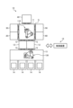
- FIG. 1 is a system configuration diagram showing an example of a manufacturing system 10 in an embodiment of the present disclosure.
- the manufacturing system 10 includes a VTM (Vacuum Transfer Module) 11, a plurality of LLMs (Load Lock Modules) 12, and an EFEM (Equipment Front End Module) 13.
- a film forming apparatus 20, a film forming apparatus 30, a plasma processing apparatus 40, a film forming apparatus 50, and a heating apparatus 60 are connected to a side wall of the VTM 11 via a gate valve G.
- VTM Vauum Transfer Module
- LLMs Load Lock Modules
- EFEM Equipment Front End Module
- the film forming apparatus 20, the film forming apparatus 30, the plasma processing apparatus 40, the film forming apparatus 50, and the heating apparatus 60 are each connected to the VTM 51, but the disclosed technology is not limited to this.
- at least one of the film forming apparatus 20, the film forming apparatus 30, the plasma processing apparatus 40, the film forming apparatus 50, and the heating apparatus 60 may be connected to the VTM 11 in a plurality of units.
- the film forming apparatus 20 forms a graphene film on the sidewalls of the metal-containing layers on a substrate W having a pattern including a plurality of metal-containing layers formed on an underlayer and a dielectric layer formed on each of the metal-containing layers.
- the film forming apparatus 20 is an example of a first processing apparatus.
- the film forming apparatus 30 fills a thermally decomposable organic film in a groove formed by adjacent metal-containing layers on the substrate W.
- the film forming apparatus 30 is an example of a second processing apparatus.
- the plasma processing device 40 removes unnecessary organic films formed on the dielectric layer.
- the film forming apparatus 50 forms a sealing film on the organic film embedded in the grooves of the substrate W.
- the film forming apparatus 50 is an example of a third processing apparatus.
- the heating device 60 heats the substrate W to thermally decompose the organic film and detach the organic film through the sealing film, thereby forming an air gap between the groove and the sealing film.
- the heating device 60 is an example of a fourth processing device.
- a number of LLMs 12 are connected to the other side wall of the VTM 11 via gate valves G.
- two LLMs 12 are connected to the VTM 11, but the number of LLMs 12 connected to the VTM 11 may be more than two, or may be just one.
- a transfer robot 110 is disposed within the VTM 11.
- the transfer robot 110 transfers the substrate W between the film forming device 20, the film forming device 30, the plasma processing device 40, the film forming device 50, the heating device 60, and the LLM 12.
- a predetermined pressure atmosphere lower than atmospheric pressure is maintained within the VTM 11.
- each LLM 12 is connected to the VTM 11 via a gate valve G, and the other side wall is connected to the EFEM 13 via a gate valve G.
- the gate valve G is closed and the pressure inside the LLM 12 is reduced to a pressure equivalent to that inside the VTM 11.
- the gate valve G is then opened, and the substrate W in the LLM 12 is loaded into the VTM 11 by the transport robot 110.
- the transfer robot 110 transfers the substrate W from the VTM 11 into the LLM 12 via the gate valve G, which is then closed.
- the pressure inside the LLM 12 is then raised to approximately the same as the pressure inside the EFEM 13.
- the gate valve G is then opened, and the substrate W inside the LLM 12 is transferred into the EFEM 13.
- Each load port 14 is connected to a container such as a FOUP (Front Opening Unified Pod) capable of accommodating multiple substrates W.
- An aligner module that changes the orientation of the substrate W may also be provided within the EFEM 13.
- the inside of the EFEM 13 is, for example, atmospheric pressure.
- a transport robot 130 is provided inside the EFEM 13.
- the transport robot 130 transports the substrate W between the LLM 12 and a container connected to the load port 14.
- An FFU (Fan Filter Unit) or the like is provided at the top of the EFEM 13, and dry air from which particles and the like have been removed is supplied from above into the EFEM 13, forming a downflow in the EFEM 13.
- the inside of the EFEM 13 is atmospheric pressure, but in another embodiment, the pressure inside the EFEM 13 may be controlled to be positive pressure. This makes it possible to suppress the intrusion of particles and the like into the EFEM 13 from the outside.
- the control device 15 includes a memory, a processor, and an input/output interface.
- the memory stores data such as a control program and processing recipes.
- the processor reads the control program from the memory and executes it, and controls each part of the manufacturing system 10 via the input/output interface based on the recipes and other data stored in the memory.
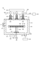
- FIG. 2 is a diagram showing an example of a film forming apparatus 20.
- a film forming apparatus 50 has the same configuration as the film forming apparatus 20 illustrated in FIG. 2.
- the film forming apparatus 20 illustrated in FIG. 2 includes a chamber 201, a mounting table 202, a gas supply mechanism 203, an exhaust device 204, and a microwave introduction device 205.
- the chamber 201 accommodates a substrate W.
- the mounting table 202 mounts the substrate W.
- the gas supply mechanism 203 supplies gas into the chamber 201.
- the exhaust device 204 exhausts gas from the chamber 201.
- the microwave introduction device 205 generates microwaves for generating plasma in the chamber 201 and introduces microwaves into the chamber 201.
- the chamber 201 is formed from a metal material such as aluminum or an alloy thereof, has a generally cylindrical shape, and has a plate-shaped top wall portion 211 and bottom wall portion 213, and a side wall portion 212 connecting these.
- the microwave introduction device 205 is provided at the top of the chamber 201, and functions as a plasma generation means that introduces electromagnetic waves (microwaves) into the chamber 201 to generate plasma.
- the microwave introduction device 205 will be described in detail later.
- the top wall 211 has a number of openings into which the microwave radiation mechanism and gas introduction section of the microwave introduction device 205, described later, are fitted.
- the side wall 212 has an inlet/outlet 214 for loading/unloading the substrate W between the chamber 201 and a transfer chamber (not shown) adjacent to the chamber 201.
- the inlet/outlet 214 is opened and closed by a gate valve G.
- the bottom wall 213 is provided with an exhaust device 204.
- the exhaust device 204 is provided on an exhaust pipe 216 connected to the bottom wall 213, and includes a vacuum pump and a pressure control valve.
- the chamber 201 is evacuated through the exhaust pipe 216 by the vacuum pump of the exhaust device 204.
- the pressure inside the chamber 201 is controlled by a pressure control valve.
- the mounting table 202 is generally disk-shaped and made of ceramics such as aluminum nitride.
- the mounting table 202 is supported by a cylindrical support member 220 and a base member 221 made of ceramics such as aluminum nitride that extend upward from the center of the bottom of the chamber 201.
- a guide ring 281 for guiding the substrate W is provided on the outer edge of the mounting table 202.
- lifting pins (not shown) for raising and lowering the substrate W are provided so as to be able to protrude and retract from the upper surface of the mounting table 202.
- a resistance heating type heater 282 is embedded inside the mounting table 202, and this heater 282 heats the substrate W placed thereon via the mounting table 202 by being powered by a heater power supply 283.
- a thermocouple (not shown) is also inserted into the mounting table 202, and the heating temperature of the substrate W can be controlled to a predetermined temperature, for example, in the range of 200 to 1000°C, based on a signal from the thermocouple.
- an electrode 284 of approximately the same size as the substrate W is embedded above the heater 282 inside the mounting table 202, and a high frequency bias power supply 222 is electrically connected to this electrode 284. A high frequency bias for attracting ions is applied from this high frequency bias power supply 222 to the mounting table 202. Note that the high frequency bias power supply 222 may not be provided depending on the characteristics of the plasma processing.
- a plurality of gas introduction nozzles 223 are fitted into the openings formed in the ceiling wall 211 of the chamber 201.
- a gas supply mechanism 203 is connected to each gas introduction nozzle 223 via a gas supply pipe 291.
- the gas supply mechanism 203 is a supply source of processing gas.
- a mixed gas containing a rare gas and a carbon-containing gas is used as the processing gas.
- argon is used as the rare gas.
- a mixed gas containing a silicon-containing gas, a reactive gas, and a rare gas is used as the processing gas.
- a mixed gas containing a silicon-containing gas, a reactive gas, and a rare gas is used as the processing gas.
- silane (SiH4), dichlorosilane (DCS), etc. are used as the silicon-containing gas.
- nitrogen, ammonia, oxygen, etc. are used as the reactive gas.
- argon, helium, etc. are used as the rare gas.
- the gas supply mechanism 203 is provided with a valve and a flow rate controller for each gas type, and the flow rate of the gas is adjusted for each gas type.
- a hydrogen-containing gas such as hydrogen gas, may be added to the processing gas.
- the microwave introduction device 205 is provided above the chamber 201 and functions as a plasma generation means that introduces electromagnetic waves (microwaves) into the chamber 201 to generate plasma.
- the microwave introduction device 205 has a ceiling wall portion 211 of the chamber 201, a microwave output portion 230, and an antenna unit 240.
- the ceiling wall portion 211 functions as a top plate.
- the microwave output portion 230 generates microwaves and distributes the microwaves to multiple paths before outputting them.
- the antenna unit 240 radiates the microwaves output from the microwave output portion 230 to the chamber 201.
- the microwave output unit 230 has a microwave power supply, a microwave oscillator, an amplifier, and a distributor.
- the microwave oscillator is solid-state and oscillates microwaves at, for example, 860 MHz (e.g., PLL oscillation).
- the microwave frequency is not limited to 860 MHz, and frequencies in the range of 700 MHz to 10 GHz, such as 2.45 GHz, 8.35 GHz, 5.8 GHz, and 1.98 GHz, can be used.
- the amplifier amplifies the microwaves oscillated by the microwave oscillator.
- the distributor distributes the microwaves amplified by the amplifier to multiple paths. The distributor distributes the microwaves while matching the impedance of the input side and output side.
- the antenna unit 240 includes multiple antenna modules. Each of the multiple antenna modules introduces microwaves distributed by a distributor in the microwave output section 230 into the chamber 201.
- the multiple antenna modules all have the same configuration.
- Each antenna module has an amplifier section 242 that mainly amplifies and outputs the distributed microwaves, and a microwave radiation mechanism 243 that radiates the microwaves output from the amplifier section 242 into the chamber 201.
- the amplifier section 242 has a phase shifter, a variable gain amplifier, a main amplifier, and an isolator.
- the phase shifter changes the phase of the microwave.
- the variable gain amplifier adjusts the power level of the microwave input to the main amplifier.
- the main amplifier is configured as a solid-state amplifier.
- the isolator separates the reflected microwaves that are reflected by the antenna section of the microwave radiation mechanism 243 (described later) and head toward the main amplifier.
- the microwave radiation mechanisms 243 are provided on the ceiling wall 211, as shown in FIG. 2, for example.
- the microwave radiation mechanism 243 has a cylindrical outer conductor and an inner conductor arranged coaxially with the outer conductor within the outer conductor.
- the microwave radiation mechanism 243 has a coaxial tube having a microwave transmission path between the outer conductor and the inner conductor, and an antenna unit that radiates microwaves into the chamber 201.
- a microwave transmitting plate 263 is fitted into the ceiling wall 211 on the underside of the antenna unit, and its underside is exposed to the internal space of the chamber 201. The microwaves that have passed through the microwave transmitting plate 263 generate plasma in the space within the chamber 201.
- the microwave radiation mechanism 243 is an example of a plasma source.
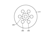
- FIG. 3 is a schematic diagram of an example of the top wall portion 211.
- seven microwave radiation mechanisms 243 are provided on the top wall portion 211, and the corresponding microwave transmission plates 263 are evenly arranged on the top wall portion 211 in a hexagonal close-packed arrangement. That is, one of the seven microwave transmission plates 263 is arranged approximately in the center of the top wall portion 211, and the other six microwave transmission plates 263 are arranged around it. These seven microwave transmission plates 263 are arranged so that the intervals between the adjacent microwave transmission plates 263 are even.
- the center of the top wall portion 211 is an example of a central region
- the periphery of the microwave radiation mechanism 243 arranged in the center of the top wall portion 211 is an example of a peripheral region. That is, one microwave radiation mechanism 243 is arranged in the central region, and six microwave radiation mechanisms 243 are arranged in the peripheral region.
- the multiple gas introduction nozzles 223 are arranged to surround the periphery of the central microwave transmission plate 263.
- the microwave radiation mechanism 243 arranged in the central region will be referred to as the central microwave radiation mechanism 243
- each of the microwave radiation mechanisms 243 arranged in the peripheral region will be referred to as the peripheral microwave radiation mechanisms 243.
- the number of microwave radiation mechanisms 243 is not limited to seven, and may be less than seven or more than seven.
- [Configuration example of film forming apparatus 30] 4 is a diagram showing an example of a film forming apparatus 30.
- the film forming apparatus 30 includes a chamber 31, an exhaust mechanism 32, a gas supply unit 33, a shower head 35, and a stage 36.
- the film forming apparatus 30 is, for example, a chemical vapor deposition (CVD) apparatus.
- CVD chemical vapor deposition
- the exhaust mechanism 32 has a vacuum pump that exhausts the gas in the chamber 31, and a pressure adjustment valve that adjusts the pressure in the chamber 31.
- the inside of the chamber 31 is controlled by the exhaust mechanism 32 to a vacuum atmosphere of a predetermined pressure.
- a gas supply unit 33 that supplies multiple types of raw material monomers is connected to the chamber 31 via a shower head 35.
- the multiple types of raw material monomers are, for example, isocyanate and amine.
- Isocyanate is an example of a first monomer
- amine is an example of a second monomer.
- the gas supply unit 33 has a raw material supply source 330a, a raw material supply source 330b, a vaporizer 331a, and a vaporizer 331b.
- the raw material supply source 330a contains, for example, an isocyanate liquid.
- the raw material supply source 330b contains, for example, an amine liquid.
- the vaporizer 331a vaporizes the isocyanate liquid supplied from the raw material supply source 330a.
- the isocyanate vapor vaporized by the vaporizer 331a is introduced into the shower head 35 via the pipe 34a.
- the vaporizer 331b vaporizes the amine liquid supplied from the raw material supply source 330b.
- the amine vapor vaporized by the raw material supply source 330b is introduced into the shower head 35 via the pipe 34b.
- the shower head 35 is provided, for example, at the top of the chamber 31, and has a number of outlets formed on the bottom surface.
- the shower head 35 ejects the isocyanate vapor introduced via the pipe 34a and the amine vapor introduced via the pipe 34b in a shower-like manner from separate outlets into the chamber 31.
- a stage 36 is provided within the chamber 31.
- the stage 36 has a temperature control mechanism (not shown).
- a substrate W is placed on the stage 36, which is brought into the chamber 31 through an opening 31a formed in the side wall of the chamber 31.
- the opening 31a is opened and closed by a gate valve G.
- the stage 36 has a temperature control mechanism, which controls the temperature of the substrate W so that it becomes a temperature suitable for vapor deposition polymerization of the raw material monomer supplied from the gas supply unit 33.
- the temperature suitable for vapor deposition polymerization can be determined according to the type of raw material monomer.
- the temperature suitable for vapor deposition polymerization is, for example, within the range of 60°C to 100°C.
- a vapor deposition polymerization reaction of two types of raw material monomers occurs on the surface of the substrate W, forming an organic polymer film on the surface of the substrate W.
- the two types of raw material monomers are isocyanate and amine, an organic polymer film having polyurea bonds is formed on the surface of the substrate W.
- FIG. 5 is a diagram showing an example of a plasma processing apparatus 40.
- the plasma processing apparatus 40 has a chamber 41 formed of a conductive material.
- the chamber 41 is grounded.
- An exhaust mechanism 42 is connected to the chamber 41, and the gas inside the chamber 41 is exhausted by the exhaust mechanism 42, and the inside of the chamber 41 is controlled to a predetermined pressure.
- a stage 43 on which the substrate W is placed is provided in the chamber 41.
- the substrate W is placed on the stage 43 and is brought into the chamber 41 through an opening 41a formed in the side wall of the chamber 41.
- the opening 41a is opened and closed by a gate valve G.
- a heater 43a for heating the substrate W is provided in the stage 43.
- the stage 43 is electrically connected to the bottom of the chamber 41 and functions as an anode electrode.
- a shower head 44 is provided above the stage 43 so as to face the upper surface of the stage 43.
- the shower head 44 is supported on the upper part of the chamber 41 via an insulating member 44A.
- a power source 45 that supplies high-frequency power for generating plasma is connected to the shower head 44.
- the shower head 44 functions as a cathode electrode with respect to the stage 43.
- the gas supply source 46 supplies the process gas.
- the flow rate controller 47 adjusts the flow rate of the process gas supplied from the gas supply source 46 and supplies it into the diffusion space 44B of the shower head 44.
- the process gas supplied into the diffusion space 44B diffuses within the diffusion space 44B and is supplied in a shower-like manner into the chamber 41 from a plurality of outlets 44C formed on the lower surface of the diffusion space 44B.
- one gas supply source 46 and one flow rate controller 47 are shown in FIG. 5, in reality, a set of the gas supply source 46 and the flow rate controller 47 is provided for each type of gas used.
- the processing gas supplied into the chamber 41 through the shower head 44 is converted into plasma by high-frequency power supplied into the chamber 41 from the power source 45. Then, the ions and activated species contained in the plasma are used to perform processing such as etching on the substrate W.
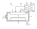
- FIG. 6 is a diagram showing an example of a heating device 60.
- the heating device 60 has a chamber 61, an exhaust pipe 62, a supply pipe 63, a stage 64, and a lamp house 65.
- a lamp house 65 is provided at a position opposite the surface of the stage 64 on which the substrate W is placed.
- a lamp 65a such as an infrared lamp is disposed inside the lamp house 65.
- a gas supply unit 63a is connected to the side wall of the chamber 61 via a supply pipe 63.
- the gas supply unit 63a supplies an inert gas such as N2 gas into the chamber 61 via the supply pipe 63.
- An opening 61a for loading and unloading the substrate W is also formed in the side wall of the chamber 61.
- the opening 61a is opened and closed by a gate valve G.
- An exhaust device 66 is connected to the bottom of the chamber 61 via an exhaust pipe 62.
- the exhaust device 66 has a pressure adjustment valve.
- the exhaust device 66 exhausts the gas in the chamber 61 and controls the pressure adjustment valve so that the pressure inside the chamber 61 is set to a predetermined pressure.
- the lamp 65a can be turned on to heat the substrate W to a predetermined temperature in the inert gas atmosphere.
- FIG. 7 is a flowchart showing an example of a method for manufacturing a semiconductor device according to the first embodiment.
- the manufacturing method shown in Fig. 7 is realized by the control device 15 controlling each part of the manufacturing system 10.
- the following description will be given with reference to Figs. 8A to 8G.
- Step S100 is an example of process a).
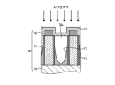
- the substrate W having a structure such as that shown in FIG. 8A is loaded into the plasma processing apparatus 200 by the transfer robot 110 in the VTM 11.
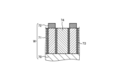
- the substrate W has a pattern including a plurality of metal-containing layers 71 formed on the underlayer 70 and a dielectric layer 72 formed on each of the metal-containing layers 71.
- a semiconductor device is manufactured from the substrate W.
- at least the surface of the underlayer 70 is formed of, for example, TiN or TaN.
- the metal-containing layer 71 contains at least one of, for example, Ru, Co, Cu, Mo, Ni, or W.
- the metal-containing layer 71 is used, for example, as wiring in the semiconductor device.
- the dielectric layer 72 is, for example, a silicon-containing film such as a silicon nitride film.
- Step S101 is an example of process b).
- a modifying gas is supplied into the chamber 201 to modify the sidewalls of the metal-containing layers 71.
- the pretreatment is performed by the film forming apparatus 20 under the following processing conditions, for example.
- Pressure in chamber 201 50 mTorr to 1 Torr (6.7 to 133 Pa)
- Temperature of substrate W 250 to 550° C. Processing time: 5 seconds to 15 minutes
- the pretreatment in step S101 reduces an oxide film that was unintentionally formed on the surface of the sidewall of the metal-containing layer 71 during transportation of the substrate W, etc.
- the modifying gas used in the pretreatment in step S101 includes an inert gas and a hydrogen-containing gas.
- the inert gas includes at least one of a rare gas such as He gas or Ar gas, or N2 gas
- the hydrogen-containing gas includes at least one of H2 gas or NH3 gas.
- plasma may be used in the pretreatment in step S101.
- the pretreatment using plasma is performed under the following processing conditions, for example.
- Pressure in chamber 201 50 mTorr to 1 Torr (6.7 to 133 Pa)
- Flow rate of hydrogen-containing gas e.g., H2 gas
- Microwave power 100-1500W
- Temperature of substrate W 250 to 550° C.
- Processing time 5 seconds to 15 minutes
- Step S102 is an example of process c).
- plasma is generated from a first process gas containing a carbon-containing gas in the chamber 201, and the graphene film 73 is formed on the side wall of the metal-containing layer 71 by using the generated plasma.
- the graphene film 73 is formed by the film formation apparatus 20 under the following process conditions, for example.
- a graphene film 73 is formed on the sidewall of the metal-containing layer 71, as shown in FIG. 8B, for example.
- the pressure in the chamber 201 is more preferably 50 mTorr to 100 mTorr (6.67 Pa to 13.3 Pa).
- the microwave power is more preferably 300 W to 1500 W.
- the first process gas includes a carbon-containing gas and an inert gas.
- the first process gas may include a hydrogen-containing gas such as H2 gas or NH3 gas.
- the carbon-containing gas is a hydrocarbon gas (e.g., C2H2 gas or C2H4 gas) represented by CxHy (x and y are natural numbers), and the inert gas is a rare gas such as He gas or Ar gas.
- a hydrocarbon gas e.g., C2H2 gas or C2H4 gas
- CxHy x and y are natural numbers
- the inert gas is a rare gas such as He gas or Ar gas.
- step S103 the substrate W is transported from the film forming apparatus 20 to the film forming apparatus 30 (step S103).
- step S103 the substrate W is transported out of the chamber 201 of the film forming apparatus 20 by the transport robot 110 in the VTM 11 and is transported into the chamber 31 of the film forming apparatus 30.
- Step S104 is an example of process d).
- a first monomer and a second monomer are supplied into the chamber 31, and a vapor deposition polymerization reaction of the first monomer and the second monomer occurs on the surface of the substrate W, forming a thermally decomposable polymer organic film on the surface of the substrate W.
- the first monomer is, for example, an isocyanate
- the second monomer is, for example, an amine
- the polymer organic film has a polyurea bond.
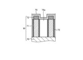
- an organic film 74 is embedded in the groove formed by adjacent metal-containing layers 71, as shown in FIG. 8C, for example.
- step S104 an organic film 74 is formed on the surface of the substrate W under, for example, the following processing conditions.
- Pressure in chamber 31 0.5 to 20 Torr (66.7-2666Pa)
- Flow rate of isocyanate vapor 1 to 20 sccm (0.0017-0.034Pa ⁇ m 3 /s)
- Flow rate of amine vapor 1 to 20 sccm (0.0017-0.034Pa ⁇ m 3 /s)
- Temperature of substrate W 40 to 150° C.
- step S105 the substrate W is transported from the film forming apparatus 30 to the plasma processing apparatus 40 (step S105).
- step S105 the substrate W is removed from the chamber 31 of the film forming apparatus 30 by the transport robot 110 in the VTM 11 and is transported into the chamber 41 of the plasma processing apparatus 40.
- Step S106 is an example of process h).
- plasma is generated from the processing gas in the chamber 41.
- the unnecessary organic film 74 formed on the dielectric layer 72 is removed by the generated plasma, for example, as shown in FIG. 8D. In other words, the organic film 74 is removed so as to expose the dielectric layer 72.
- step S107 the substrate W is transported from the plasma processing device 40 to the film forming device 50 (step S107).
- step S107 the substrate W is removed from the chamber 41 of the plasma processing device 40 by the transport robot 110 in the VTM 11 and is transported into the chamber 201 of the film forming device 50.
- Step S108 is an example of process e).
- plasma is generated in the chamber 201 from a processing gas containing, for example, organic aminosilane.
- a sealing film 75 is formed on the organic film 74, as shown in FIG. 8E.
- the sealing film 75 is, for example, a silicon oxide film.
- the sealing film 75 may be another silicon-containing film, such as a silicon nitride film.
- the sealing film 75 is formed by the film forming apparatus 50 under, for example, the following processing conditions.
- step S109 the substrate W is transported from the film forming apparatus 50 to the heating apparatus 60 (step S109).
- step S109 the substrate W is transported out of the chamber 201 of the film forming apparatus 50 by the transport robot 110 in the VTM 11 and is transported into the chamber 61 of the heating apparatus 60.
- Step S110 is an example of process f).
- the substrate W is heated to pyrolyze the organic film 74, and the organic film 74 is detached through the sealing film 75.
- an air gap 74a is formed between the groove formed by the adjacent metal-containing layers 71 and the sealing film 75.
- step S111 the substrate W is transported from the heating device 60 to the film forming device 50 (step S111).
- step S111 the substrate W is removed from the chamber 61 of the heating device 60 by the transport robot 110 in the VTM 11, and is transported back into the chamber 201 of the film forming device 50.
- a protective film is formed on the sealing film 75 (step S112).
- plasma is generated in the chamber 201 from a process gas containing, for example, an organic aminosilane.
- a protective film 76 is formed on the sealing film 75, as shown in, for example, FIG. 8G.
- the protective film 76 is, for example, a silicon nitride film.
- the protective film 76 is formed by the film forming apparatus 50 under, for example, the following process conditions.
- step S113 the substrate W is removed from the film forming apparatus 50 (step S113). Then, the method for manufacturing a semiconductor device shown in this flowchart is completed.
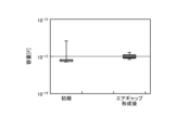
- Fig. 9 is a diagram showing an example of the state of the air gap 74a for each thickness of the sealing film 75.
- the thickness of the sealing film 75 is thicker than 1.2 nm.
- the thickness of the sealing film 75 is 2.4 nm, as shown in FIG. 9, even after the substrate W is heated, the organic film 74 in the groove formed by the adjacent metal-containing layers 71 is not completely detached and remains. Therefore, it is preferable that the thickness of the sealing film 75 is thinner than 2.4 nm.
- the thickness of the sealing film 75 was 1.6 nm and 2.0 nm, as shown in FIG. 9, for example, no organic film 74 was observed in the groove formed by adjacent metal-containing layers 71. Furthermore, the sealing film 75 was not torn. Therefore, it is preferable that the thickness of the sealing film 75 is 1.2 nm or more and 2.0 nm or less.
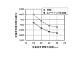
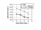
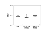
- the resistance value of the metal-containing layer 71 was measured when the air gap 74a was formed without forming the graphene film 73 on the side wall of the metal-containing layer 71, and the results shown in Fig. 10A and Fig. 10B were obtained.
- the metal-containing layer 71 was heated to remove the organic film 74, so that the crystal grains of the metal-containing layer 71 expanded, and the resistance value of the metal-containing layer 71 was reduced.
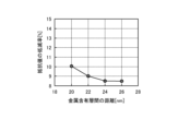
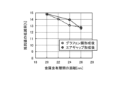
- the resistance value of the metal-containing layer 71 after the air gap 74a was formed was reduced by about 9% from the initial state.
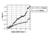
- the reduction rate of the resistance value of the metal-containing layer 71 is increased by about 5% compared to the case where the graphene film 73 is not formed on the sidewall of the metal-containing layer 71. Therefore, in this embodiment, by forming the graphene film 73 on the sidewall of the metal-containing layer 71, the resistance value of the metal-containing layer 71 used as wiring in a semiconductor device can be further reduced.
- FIG. 12A is a diagram showing an example of the capacitance between metal-containing layers 71 in the comparative example.
- FIG. 12B is a diagram showing an example of the capacitance between metal-containing layers 71 in the first embodiment.
- the capacitance between the metal-containing layers 71 is almost unchanged between the initial state and after the air gap 74a is formed.
- the initial state as shown in FIG. 8A, for example, there is a space between adjacent metal-containing layers 71.
- the resistance value of the metal-containing layer 71 can be reduced, and by forming an air gap 74a between adjacent metal-containing layers 71, the capacitance between the metal-containing layers 71 can be reduced. This makes it possible to reduce the delay of signals flowing through the metal-containing layer 71 used as wiring within a semiconductor device.
- the method for manufacturing a semiconductor device in the first embodiment includes steps a), b), c), d), e), and f).
- a substrate (substrate W) having a pattern including a plurality of metal-containing layers (metal-containing layers 71) formed on an underlayer (underlayer 70) and a dielectric layer (dielectric layer 72) formed on each of the metal-containing layers is prepared in a chamber (chamber 201).
- a modifying gas is supplied into the chamber to modify the sidewalls of each metal-containing layer.
- step c) plasma is generated from a first processing gas including a carbon-containing gas in the chamber, and a graphene film (graphene film 73) is formed on the sidewall of the metal-containing layer using the generated plasma.
- step d) a pyrolyzable organic film (organic film 74) is embedded in a groove formed by adjacent metal-containing layers.
- step e) a sealing film (sealing film 75) is formed on the organic film embedded in the groove.
- step f) the substrate is heated to thermally decompose the organic film, and the organic film is detached through the sealing film, forming an air gap (air gap 74a) between the groove and the sealing film. This makes it possible to manufacture a semiconductor device with little signal delay.
- the method for manufacturing a semiconductor device in the first embodiment described above further includes a step of removing the organic film formed on the dielectric layer, which is performed between steps d) and e). This allows an air gap of a desired shape to be formed between adjacent metal-containing layers 71.
- the thickness of the sealing film is preferably 1.6 nm or more and 2.0 nm or less. This allows an air gap of the desired shape to be formed between adjacent metal-containing layers 71.
- the sealing film may be a silicon oxide film or a silicon nitride film. This makes it possible to remove the organic film embedded between adjacent metal-containing layers 71.
- the modifying gas contains an inert gas and a hydrogen-containing gas, and the flow rate ratio of the inert gas to the hydrogen-containing gas is preferably in the range of 200:2 to 50:50. This makes it possible to modify the sidewall of the metal-containing layer 71 so that the graphene film can be more easily attached.
- the inert gas contained in the modifying gas contains at least one of He gas, Ar gas, and N2 gas.
- the hydrogen-containing gas contained in the modifying gas contains at least one of H2 gas and NH3 gas. This makes it possible to modify the sidewall of the metal-containing layer 71 so that the graphene film can be easily attached.
- the temperature of the substrate in step c) is preferably 250° C. or higher and 550° C. or lower. This allows the graphene film to be efficiently formed on the sidewall of the metal-containing layer 71.
- the temperature of the substrate in step d) is preferably 40° C. or higher and 150° C. or lower. This allows the organic film to be efficiently embedded in the grooves formed by adjacent metal-containing layers.
- the temperature of the substrate in step e) is preferably 20°C or higher and 100°C or lower. This allows the sealing film to be efficiently formed on the organic film.
- the temperature of the substrate in step f) is preferably 350°C or higher and 450°C or lower. This allows the organic film to be efficiently detached through the sealing film.
- the surface of the underlayer is TiN or TaN. This makes it possible to suppress the formation of a graphene film on the underlayer.
- the metal-containing layer contains at least one of Ru, Co, and Cu. This allows a graphene film to be efficiently formed on the metal-containing layer.
- step d gases of the first monomer and the second monomer are supplied into the chamber, and the organic film is embedded in the groove by vapor deposition polymerization of the first monomer and the second monomer. This allows the organic film to be embedded efficiently in the groove formed by adjacent metal-containing layers.
- the first monomer is an isocyanate
- the second monomer is an amine
- the organic film contains a urea bond. This allows the organic film to be efficiently detached through the sealing film.
- the first embodiment described above is a semiconductor device manufacturing system (manufacturing system 10) that includes a first processing device (film forming device 20), a second processing device (film forming device 30), a third processing device (film forming device 50), a fourth processing device (heating device 60), and a control device (control device 15) that controls the first processing device, the second processing device, the third processing device, and the fourth processing device.
- the control device executes steps a), b), c), d), e), and f).
- a substrate (substrate W) having a pattern including a plurality of metal-containing layers (metal-containing layers 71) formed on an underlayer (underlayer 70) and a dielectric layer (dielectric layer 72) formed on each of the metal-containing layers is prepared in a chamber (chamber 201) of the first processing device.
- a modifying gas is supplied into the chamber to modify the sidewalls of each metal-containing layer.
- plasma is generated from a first processing gas containing a carbon-containing gas in the chamber, and the generated plasma is used to form a graphene film (graphene film 73) on the side wall of the metal-containing layer.
- a thermally decomposable organic film (organic film 74) is embedded in a groove formed by adjacent metal-containing layers using a second processing device.
- a sealing film (sealing film 75) is formed on the organic film embedded in the groove using a third processing device.
- an air gap (air gap 74a) is formed between the groove and the sealing film by thermally decomposing the organic film by heating the substrate using a fourth processing device, and detaching the organic film through the sealing film. This allows the manufacture of a semiconductor device with little signal delay.
- the organic film 74 in the groove formed by the adjacent metal-containing layers 71 may not be completely removed and may remain as a residue.
- the residue in the groove may become conductive due to heating. Therefore, the leakage current after the air gap 74a is formed may be larger than the leakage current at the stage where the graphene film 73 is formed, as shown in FIG. 13, for example. Therefore, in the second embodiment, in order to remove the residue after the air gap 74a is formed, a process for removing the organic film 74 is performed after the substrate W is heated to form the air gap 74a.
- Fig. 14 is a flowchart showing an example of a method for manufacturing a semiconductor device according to the second embodiment.
- the manufacturing method shown in Fig. 14 is realized by a control device 15 controlling each part of the manufacturing system 10.
- the processes in Fig. 14 denoted by the same reference numerals as those in Fig. 7 are the same as those described using Fig. 7 except for the points described below, and therefore will not be described again.
- step S120 the substrate W is transported from the heating device 60 to the plasma processing device 40 (step S120).
- step S120 the substrate W is transported by the transport robot 110 in the VTM 11 out of the chamber 61 of the heating device 60 and into the chamber 41 of the plasma processing device 40.
- Step S121 is an example of process g).
- plasma is generated from a processing gas in the chamber 41.
- the processing gas is Ar gas.
- the processing gas used in step S121 is an example of a third processing gas that does not contain oxygen. Note that the processing gas used in step S121 may be a rare gas other than Ar, or may be a gas that contains at least one of a rare gas, N2 gas, or H2 gas.
- step S121 plasma is generated under the following processing conditions, for example.
- Pressure in chamber 41 0.5 to 5 Torr (66.7-667Pa)
- Processing gas: Ar 200 to 2000 sccm (0.34-3.4Pa ⁇ m 3 /s)
- High frequency power 50-500W
- Temperature of substrate W 300 to 400° C.
- the generated plasma is irradiated onto the substrate W.
- This causes active species contained in the plasma to be supplied to the residue 77 remaining in the air gap 74a, decomposing the residue 77.
- the decomposed residue 77 is detached through the sealing film 75.
- step S122 the substrate W is transported from the plasma processing device 40 to the film forming device 50 (step S122).
- step S122 the substrate W is removed from the chamber 41 of the plasma processing device 40 by the transport robot 110 in the VTM 11 and is transported into the chamber 201 of the film forming device 50. Then, the processes from step S112 onwards are performed.
- FIG. 16 is a diagram showing an example of leakage current in the second embodiment.
- the leakage current when plasma is applied after the air gap 74a is formed is reduced compared to before the plasma is applied, as shown in FIG. 16 for example. Therefore, by applying plasma after the air gap 74a is formed, the leakage current between adjacent metal-containing layers 71 can be reduced.
- the method for manufacturing a semiconductor device in the second embodiment further includes step g).
- step g) after the air gap is formed in step f), plasma is irradiated into the groove through the sealing film. This makes it possible to reduce the leakage current between adjacent metal-containing layers 71.
- step g) of the second embodiment described above plasma generated from a third process gas that does not contain oxygen is irradiated into the groove through the sealing film.
- the third process gas contains at least one of a rare gas, N2 gas, and H2 gas. This makes it possible to reduce the leakage current between adjacent metal-containing layers 71.
- the substrate W is irradiated with plasma generated from a processing gas that does not contain oxygen, but the disclosed technology is not limited to this.
- the substrate W may be irradiated with plasma generated from a processing gas that contains oxygen. This makes it possible to more efficiently remove the residue 77 remaining in the air gap 74a.
- the graphene film 73 may also be removed due to active species derived from oxygen contained in the plasma, depending on the conditions. Furthermore, the sidewall of the metal-containing layer 71 may be oxidized due to active species derived from oxygen contained in the plasma, depending on the conditions, and the resistance value of the metal-containing layer 71 may increase. Therefore, when plasma generated from a processing gas containing oxygen is used to remove the residue 77, it is preferable to perform the processing under the following processing conditions.
- the graphene film 73 is formed using a film forming apparatus 20 having multiple microwave radiation mechanisms 543, but the disclosed technology is not limited to this.
- the graphene film 73 may be formed using a film forming apparatus having, for example, one microwave radiation mechanism.
- the deposition apparatus 20 that deposits the graphene film 73 using microwave plasma as the plasma source has been described as an example, but the disclosed technology is not limited to this.
- the plasma source is not limited to microwave plasma, and any plasma source can be used, such as capacitively coupled plasma, inductively coupled plasma, magnetron plasma, etc.
- an organic film 74 of a thermally decomposable polymer having a urea bond (-NH-CO-NH-) is formed on the surface of the substrate W using an isocyanate as the first monomer and an amine as the second monomer, but the disclosed technology is not limited to this.
- an organic film of a thermally decomposable polymer having a 2-aminoethanol bond (-NH-CH2-CH(OH)-) may be formed on the surface of the substrate W using an epoxide as the first monomer and an amine as the second monomer.
- an organic film of a thermally decomposable polymer having a urethane bond may be formed on the surface of the substrate W using an isocyanate as the first monomer and an alcohol as the second monomer.
- an organic film of a thermally decomposable polymer having an amide bond may be formed on the surface of the substrate W using an acyl halide as the first monomer and an amine as the second monomer.
- a carboxylic acid anhydride may be used as the first monomer and an amine as the second monomer to form an organic film of a thermally decomposable polymer having imide bonds (-CO-N(-)-CO-) on the surface of the substrate W.
- (Appendix 1) a) providing a substrate in a chamber having a pattern including a plurality of metal-containing layers formed on an underlayer and a dielectric layer formed on each of the metal-containing layers; b) modifying a sidewall of each of the metal-containing layers by supplying a modification gas into the chamber; c) generating a plasma from a first process gas including a carbon-containing gas in the chamber, and forming a graphene film on the sidewall of the metal-containing layer using the generated plasma; d) filling grooves formed by adjacent metal-containing layers with a thermally decomposable organic film; e) forming a sealing film on the organic film embedded in the groove; f) heating the substrate to thermally decompose the organic film and detach the organic film through the sealing film, thereby forming an air gap between the groove and the sealing film.
- a flow rate ratio of the inert gas to the hydrogen-containing gas is in a range of 200:2 to 50:50.
- Appendix 11 11.
- Appendix 12 12.
- Appendix 13 13.
- the method for manufacturing a semiconductor device according to claim 1, wherein the temperature of the substrate in the step c) is 250° C. or higher and 550° C. or lower.
- Appendix 14 14.
- (Appendix 17) 17 17. The method for manufacturing a semiconductor device according to claim 1, wherein a surface of the underlayer is TiN or TaN. (Appendix 18) 18.
- Appendix 19 19. The method for manufacturing a semiconductor device according to any one of appendixes 1 to 18, wherein in the step d), gases of a first monomer and a second monomer are supplied into the chamber, and the organic film is embedded in the groove by vapor deposition polymerization of the first monomer and the second monomer.
- the first monomer is an isocyanate; the second monomer is an amine; 20.
- the control device includes: a) providing a substrate having a pattern including a plurality of metal-containing layers formed on an underlayer and a dielectric layer formed on each of the metal-containing layers in a chamber of the first processing apparatus; b) modifying a sidewall of each of the metal-containing layers by supplying a modification gas into the chamber; c) generating a plasma from a first process gas including a carbon-containing gas in the chamber, and forming a graphene film on the sidewall of the metal-containing layer using the generated plasma; d) filling grooves formed by adjacent metal-containing layers with a thermally decomposable organic film using the second processing apparatus; e) forming a sealing film on the organic film embedded in the groove by using the third processing apparatus; f) using the fourth processing apparatus, heating the substrate
Landscapes
- Engineering & Computer Science (AREA)
- Physics & Mathematics (AREA)
- Condensed Matter Physics & Semiconductors (AREA)
- General Physics & Mathematics (AREA)
- Manufacturing & Machinery (AREA)
- Computer Hardware Design (AREA)
- Microelectronics & Electronic Packaging (AREA)
- Power Engineering (AREA)
- Internal Circuitry In Semiconductor Integrated Circuit Devices (AREA)
- Formation Of Insulating Films (AREA)
- Chemical Vapour Deposition (AREA)
Abstract
半導体装置の製造方法は、工程a)、工程b)、工程c)、工程d)、工程e)、および工程f)を含む。工程a)では、下地層上に形成された複数の金属含有層と、それぞれの金属含有層上に形成された誘電体層とを含むパターンを有する基板をチャンバ内に準備する。工程b)では、チャンバ内に改質ガスを供給し、それぞれの金属含有層の側壁を改質する。工程c)では、チャンバ内において炭素含有ガスを含む第1の処理ガスから生成されたプラズマを用いて金属含有層の側壁にグラフェン膜を形成する。工程d)では、隣り合う金属含有層によって形成される溝に、熱分解可能な有機膜を埋め込む。工程e)では、溝に埋め込まれた有機膜の上に封止膜を形成する。工程f)では、基板を加熱することで有機膜を熱分解させ、封止膜を介して有機膜を脱離させ、溝と封止膜との間にエアギャップを形成する。
Description
本開示の種々の側面および実施形態は、半導体装置の製造方法および製造システムに関する。
例えば下記特許文献1には、「本開示の一側面は、半導体装置の製造方法であって、第1の積層工程と、第2の積層工程と、脱離工程とを含む。第1の積層工程では、凹部が形成された基板上に、熱分解可能な有機材料が積層される。第2の積層工程では、有機材料の上にシリコン窒化膜が積層される。脱離工程では、基板を予め定められた温度に加熱することにより有機材料を熱分解させ、シリコン窒化膜の下層の有機材料を、シリコン窒化膜を介して脱離させることによりエアギャップが形成される。」ことが開示されている。
本開示は、信号の遅延が少ない半導体装置を製造することができる半導体装置の製造方法および製造システムを提供する。
本開示の一側面は、半導体装置の製造方法であって、工程a)と、工程b)と、工程c)と、工程d)と、工程e)と、工程f)とを含む。工程a)では、下地層上に形成された複数の金属含有層と、それぞれの金属含有層上に形成された誘電体層とを含むパターンを有する基板がチャンバ内に準備される。工程b)では、チャンバ内に改質ガスを供給することにより、それぞれの金属含有層の側壁が改質される。工程c)では、チャンバ内において炭素含有ガスを含む第1の処理ガスからプラズマを生成し、生成したプラズマを用いて金属含有層の側壁にグラフェン膜が形成される。工程d)では、隣り合う金属含有層によって形成される溝に、熱分解可能な有機膜が埋め込まれる。工程e)では、溝に埋め込まれた有機膜の上に封止膜が形成される。工程f)では、基板を加熱することにより有機膜を熱分解させ、封止膜を介して有機膜を脱離させることにより、溝と封止膜との間にエアギャップが形成される。
本開示の種々の側面および実施形態によれば、信号の遅延が少ない半導体装置を製造することができる。
以下に、開示される半導体装置の製造方法および製造システムの実施形態について、図面に基づいて詳細に説明する。なお、以下の実施形態により、開示される半導体装置の製造方法および製造システムが限定されるものではない。
近年の半導体装置の高機能化および高密度化に伴い、内部の配線の細線化が進み、配線抵抗が増加する傾向にある。また、半導体装置の高密度化に伴い、内部の配線の間隔が狭くなり、配線容量が増加する傾向にある。配線抵抗および配線容量が増加すると、配線を流れる信号の遅延が増加し、信号の品質が劣化する。そのため、半導体装置の内部の配線の配線抵抗および配線容量を低減することが求められている。
そこで、本開示は、信号の遅延が少ない半導体装置を製造することができる技術を提供する。
(第1の実施形態)
[製造システム10の構成例]
図1は、本開示の一実施形態における製造システム10の一例を示すシステム構成図である。製造システム10は、VTM(Vacuum Transfer Module)11、複数のLLM(Load Lock Module)12、およびEFEM(Equipment Front End Module)13を備える。VTM11の側壁には、ゲートバルブGを介して、成膜装置20、成膜装置30、プラズマ処理装置40、成膜装置50、および加熱装置60が接続されている。なお、図1の例では、VTM51に成膜装置20、成膜装置30、プラズマ処理装置40、成膜装置50、および加熱装置60がそれぞれ1台ずつ接続されているが、開示の技術はこれに限られない。他の例として、VTM11には、成膜装置20、成膜装置30、プラズマ処理装置40、成膜装置50、および加熱装置60の少なくとも1つが複数接続されてもよい。
成膜装置20は、下地層上に形成された複数の金属含有層と、それぞれの金属含有層上に形成された誘電体層とを含むパターンを有する基板Wにおいて、金属含有層の側壁にグラフェン膜を形成する。成膜装置20は、第1の処理装置の一例である。
成膜装置30は、基板Wにおいて隣り合う金属含有層によって形成される溝に、熱分解可能な有機膜を埋め込む。成膜装置30は、第2の処理装置の一例である。
プラズマ処理装置40は、誘電体層の上に形成された不要な有機膜を除去する。
成膜装置50は、基板Wの溝に埋め込まれた有機膜の上に封止膜を形成する。成膜装置50は、第3の処理装置の一例である。
加熱装置60は、基板Wを加熱することにより有機膜を熱分解させ、封止膜を介して有機膜を脱離させることにより、溝と封止膜との間にエアギャップを形成する。加熱装置60は、第4の処理装置の一例である。
VTM11の他の側壁には、ゲートバルブGを介して複数のLLM12が接続されている。図1の例では、VTM11に2台のLLM12が接続されているが、VTM11に接続されるLLM12の数は、2台より多くてもよく、1台であってもよい。
VTM11内には、搬送ロボット110が配置されている。搬送ロボット110は、成膜装置20、成膜装置30、プラズマ処理装置40、成膜装置50、加熱装置60、およびLLM12の間で基板Wを搬送する。VTM11内は、大気圧よりも低い予め定められた圧力雰囲気に保たれている。
それぞれのLLM12の1つの側壁には、ゲートバルブGを介してVTM11が接続されており、他の1つの側壁には、ゲートバルブGを介してEFEM13が接続されている。ゲートバルブGを介してEFEM13からLLM12内に基板Wが搬入された場合、ゲートバルブGが閉じられ、LLM12内の圧力がVTM11内の圧力と同程度の圧力まで下げられる。そして、ゲートバルブGが開かれ、LLM12内の基板Wが搬送ロボット110によってVTM11内へ搬出される。
また、LLM12内の圧力がVTM11内の圧力と同程度の圧力となっている状態で、搬送ロボット110によってゲートバルブGを介してVTM11からLLM12内に基板Wが搬入され、ゲートバルブGが閉じられる。そして、LLM12内の圧力がEFEM13内と同程度の圧力まで上げられる。そして、ゲートバルブGが開かれ、LLM12内の基板WがEFEM13内へ搬出される。
ゲートバルブGが設けられたEFEM13の側壁と反対側のEFEM13の側壁には、複数のロードポート14が設けられている。それぞれのロードポート14には、複数の基板Wを収容可能なFOUP(Front Opening Unified Pod)等の容器が接続される。なお、EFEM13内には、基板Wの向きを変更するアライナモジュール等が設けられてもよい。
EFEM13内は、例えば大気圧である。EFEM13内には、搬送ロボット130が設けられている。搬送ロボット130は、LLM12とロードポート14に接続された容器との間で基板Wを搬送する。EFEM13の上部には、FFU(Fan Filter Unit)等が設けられており、パーティクル等が除去されたドライエアが上部からEFEM13内に供給され、EFEM13内にダウンフローが形成される。なお、本実施形態において、EFEM13内は大気圧であるが、他の形態として、EFEM13内の圧力は、陽圧となるように制御されてもよい。これにより、外部からEFEM13内へのパーティクル等の侵入を抑制することができる。
制御装置15は、メモリ、プロセッサ、および入出力インターフェイスを備える。メモリには、制御プログラムおよび処理レシピ等のデータが格納される。プロセッサは、制御プログラムをメモリから読み出して実行し、メモリに格納されたレシピ等に基づいて、入出力インターフェイスを介して製造システム10の各部を制御する。
[成膜装置20および成膜装置50の構成例]
図2は、成膜装置20の一例を示す図である。成膜装置50は、図2に例示された成膜装置20と同様の構成である。図2に例示される成膜装置20は、チャンバ201と、載置台202と、ガス供給機構203と、排気装置204と、マイクロ波導入装置205とを有する。チャンバ201は、基板Wを収容する。載置台202は、基板Wを載置する。ガス供給機構203は、チャンバ201内にガスを供給する。排気装置204は、チャンバ201内のガスを排気する。マイクロ波導入装置205は、チャンバ201内にプラズマを生成させるためのマイクロ波を発生させるとともに、チャンバ201内にマイクロ波を導入する。
図2は、成膜装置20の一例を示す図である。成膜装置50は、図2に例示された成膜装置20と同様の構成である。図2に例示される成膜装置20は、チャンバ201と、載置台202と、ガス供給機構203と、排気装置204と、マイクロ波導入装置205とを有する。チャンバ201は、基板Wを収容する。載置台202は、基板Wを載置する。ガス供給機構203は、チャンバ201内にガスを供給する。排気装置204は、チャンバ201内のガスを排気する。マイクロ波導入装置205は、チャンバ201内にプラズマを生成させるためのマイクロ波を発生させるとともに、チャンバ201内にマイクロ波を導入する。
チャンバ201は、例えばアルミニウムまたはその合金等の金属材料によって形成され、略円筒形状をなしており、板状の天壁部211および底壁部213と、これらを連結する側壁部212とを有している。マイクロ波導入装置205は、チャンバ201の上部に設けられ、チャンバ201内に電磁波(マイクロ波)を導入してプラズマを生成するプラズマ生成手段として機能する。マイクロ波導入装置205については後で詳細に説明する。
天壁部211には、マイクロ波導入装置205の後述するマイクロ波放射機構およびガス導入部が嵌め込まれる複数の開口部を有している。側壁部212は、チャンバ201に隣接する搬送室(図示せず)との間で基板Wの搬入出を行うための搬入出口214を有している。搬入出口214はゲートバルブGにより開閉される。底壁部213には排気装置204が設けられている。排気装置204は底壁部213に接続された排気管216に設けられ、真空ポンプと圧力制御バルブを備えている。排気装置204の真空ポンプにより排気管216を介してチャンバ201内が排気される。チャンバ201内の圧力は圧力制御バルブにより制御される。
載置台202は、略円板状をなしており、窒化アルミニウム等のセラミックスによって形成される。載置台202は、チャンバ201の底部中央から上方に延びる円筒状の窒化アルミニウム等のセラミックスによって形成される支持部材220および基部部材221により支持されている。載置台202の外縁部には基板Wをガイドするためのガイドリング281が設けられている。また、載置台202の内部には、基板Wを昇降するための昇降ピン(図示せず)が載置台202の上面に対して突没可能に設けられている。
さらに、載置台202の内部には抵抗加熱型のヒータ282が埋め込まれており、このヒータ282はヒータ電源283から給電されることにより載置台202を介してその上の基板Wを加熱する。また、載置台202には、熱電対(図示せず)が挿入されており、熱電対からの信号に基づいて、基板Wの加熱温度を、例えば200~1000℃の範囲の所定の温度に制御可能となっている。さらに、載置台202内のヒータ282の上方には、基板Wと同程度の大きさの電極284が埋設されており、この電極284には、高周波バイアス電源222が電気的に接続されている。この高周波バイアス電源222から載置台202に、イオンを引き込むための高周波バイアスが印加される。なお、高周波バイアス電源222はプラズマ処理の特性によっては設けなくてもよい。
チャンバ201の天壁部211に形成された開口部には、複数のガス導入ノズル223が嵌め込まれている。それぞれのガス導入ノズル223には、ガス供給配管291を介してガス供給機構203が接続されている。ガス供給機構203は、処理ガスの供給源である。例えばグラフェンの成膜を行う場合、処理ガスとしては、希ガスおよび炭素含有ガスを含む混合ガスが用いられる。希ガスとしては、例えばアルゴンが用いられる。炭素含有ガスとしては、例えばエチレン(C2H4)等のCxHy(x,yは自然数)で表される炭化水素ガスが用いられる。また、例えば封止膜としてシリコン含有膜の成膜を行う場合、処理ガスとしては、シリコン含有ガス、反応ガスおよび希ガスを含む混合ガスが用いられる。シリコン含有ガスとしては、例えばシラン(SiH4)、ジクロロシラン(DCS)などが用いられる。また、反応ガスとしては、例えば、窒素、アンモニア、酸素などが用いられる。また、希ガスとしては、例えばアルゴン、ヘリウムなどが用いられる。なお、ガス供給機構203には、ガス種ごとに、バルブおよび流量制御器が設けられており、ガスの流量がそれぞれのガス種ごとに調整される。また、処理ガスには、例えば水素ガス等の水素含有ガスが添加されてもよい。
マイクロ波導入装置205は、前述のように、チャンバ201の上方に設けられ、チャンバ201内に電磁波(マイクロ波)を導入してプラズマを生成するプラズマ生成手段として機能する。
マイクロ波導入装置205は、チャンバ201の天壁部211と、マイクロ波出力部230と、アンテナユニット240とを有する。天壁部211は、天板として機能する。マイクロ波出力部230は、マイクロ波を生成するとともに、マイクロ波を複数の経路に分配して出力する。アンテナユニット240は、マイクロ波出力部230から出力されたマイクロ波をチャンバ201に放射する。
マイクロ波出力部230は、マイクロ波電源と、マイクロ波発振器と、アンプと、分配器とを有している。マイクロ波発振器はソリッドステートであり、例えば、860MHzでマイクロ波を発振(例えば、PLL発振)させる。なお、マイクロ波の周波数は、860MHzに限らず、2.45GHz、8.35GHz、5.8GHz、1.98GHz等、700MHzから10GHzの範囲のものを用いることができる。アンプは、マイクロ波発振器によって発振されたマイクロ波を増幅する。分配器は、アンプによって増幅されたマイクロ波を複数の経路に分配する。分配器は、入力側と出力側のインピーダンスを整合させながらマイクロ波を分配する。
アンテナユニット240は、複数のアンテナモジュールを含んでいる。複数のアンテナモジュールは、それぞれ、マイクロ波出力部230の分配器によって分配されたマイクロ波をチャンバ201内に導入する。複数のアンテナモジュールの構成は全て同一である。各アンテナモジュールは、分配されたマイクロ波を主に増幅して出力するアンプ部242と、アンプ部242から出力されたマイクロ波をチャンバ201内に放射するマイクロ波放射機構243とを有する。
アンプ部242は、位相器と、可変ゲインアンプと、メインアンプと、アイソレータとを有する。位相器は、マイクロ波の位相を変化させる。可変ゲインアンプは、メインアンプに入力されるマイクロ波の電力レベルを調整する。メインアンプは、ソリッドステートアンプとして構成されている。アイソレータは、後述するマイクロ波放射機構243のアンテナ部で反射されてメインアンプに向かう反射マイクロ波を分離する。
複数のマイクロ波放射機構243は、例えば図2に示されるように、天壁部211に設けられている。また、マイクロ波放射機構243は、筒状をなす外側導体および外側導体内に外側導体と同軸状に設けられた内側導体を有する。マイクロ波放射機構243は、外側導体と内側導体との間にマイクロ波伝送路を有する同軸管と、マイクロ波をチャンバ201内に放射するアンテナ部とを有する。アンテナ部の下面側には、天壁部211に嵌め込まれているマイクロ波透過板263が設けられており、その下面はチャンバ201の内部空間に露出している。マイクロ波透過板263を透過したマイクロ波は、チャンバ201内の空間にプラズマを生成する。つまり、マイクロ波放射機構243は、プラズマ源の一例である。
図3は、天壁部211の一例を模式的に示す図である。本実施形態では、例えば図3に示されるように、マイクロ波放射機構243が天壁部211に7本設けられており、これらに対応するマイクロ波透過板263は、均等に六方最密配置になるように天壁部211に配置されている。すなわち、7つのマイクロ波透過板263の中の1つは、天壁部211の略中央に配置され、その周囲に、他の6つのマイクロ波透過板263が配置されている。これら7つのマイクロ波透過板263は、隣接するマイクロ波透過板263との間隔が均等になるように配置されている。なお、天壁部211の中央は、中央領域の一例であり、天壁部211の中央に配置されたマイクロ波放射機構243の周囲は、周辺領域の一例である。つまり、マイクロ波放射機構243は、中央領域に1本配置され、周辺領域に6本配置されている。また、複数のガス導入ノズル223は、中央のマイクロ波透過板263の周囲を囲むように配置されている。なお、以下では、中央領域に配置されるマイクロ波放射機構243を中央のマイクロ波放射機構243と記載し、周辺領域に配置されるそれぞれのマイクロ波放射機構243を周辺のマイクロ波放射機構243と記載する。また、マイクロ波放射機構243の本数は7本に限られず、7本より少なくてもよく、7本より多くてもよい。
[成膜装置30の構成例]
図4は、成膜装置30の一例を示す図である。成膜装置30は、チャンバ31、排気機構32、ガス供給部33、シャワーヘッド35、およびステージ36を有する。本実施形態において、成膜装置30は、例えばCVD(Chemical Vapor Deposition)装置である。
図4は、成膜装置30の一例を示す図である。成膜装置30は、チャンバ31、排気機構32、ガス供給部33、シャワーヘッド35、およびステージ36を有する。本実施形態において、成膜装置30は、例えばCVD(Chemical Vapor Deposition)装置である。
排気機構32は、チャンバ31内のガスを排気する真空ポンプと、チャンバ31内の圧力を調整する圧力調整バルブとを有する。チャンバ31内は、排気機構32によって予め定められた圧力の真空雰囲気に制御される。
チャンバ31には、シャワーヘッド35を介して、複数種類の原料モノマーを供給するガス供給部33が接続されている。本実施形態において、複数種類の原料モノマーは、例えばイソシアネートおよびアミンである。イソシアネートは第1のモノマーの一例であり、アミンは第2のモノマーの一例である。ガス供給部33は、原料供給源330a、原料供給源330b、気化器331a、および気化器331bを有する。原料供給源330aは、例えばイソシアネートの液体を収容する。原料供給源330bは、例えばアミンの液体を収容する。
気化器331aは、原料供給源330aから供給されたイソシアネートの液体を気化させる。気化器331aによって気化されたイソシアネートの蒸気は、配管34aを介してシャワーヘッド35に導入される。また、気化器331bは、原料供給源330bから供給されたアミンの液体を気化させる。原料供給源330bによって気化されたアミンの蒸気は、配管34bを介してシャワーヘッド35に導入される。
シャワーヘッド35は、例えばチャンバ31の上部に設けられ、下面に多数の吐出口が形成されている。シャワーヘッド35は、配管34a介して導入されたイソシアネートの蒸気および配管34b介して導入されたアミンの蒸気を、別々の吐出口からチャンバ31内にシャワー状に吐出する。
チャンバ31内には、ステージ36が設けられている。ステージ36は、図示しない温度調節機構を有する。ステージ36には、チャンバ31の側壁に形成された開口31aを介してチャンバ31内に搬入された基板Wが載せられる。開口31aは、ゲートバルブGによって開閉される。ステージ36は、温度調節機構を有しており、ガス供給部33から供給された原料モノマーの蒸着重合に適した温度となるように、温度調節機構により基板Wの温度を制御する。蒸着重合に適した温度は、原料モノマーの種類に応じて定めることができる。蒸着重合に適した温度は、例えば60℃~100℃の範囲内の温度である。
このような成膜装置30を用いて、基板Wの表面において2種類の原料モノマーの蒸着重合反応を起こすことにより、基板Wの表面に重合体の有機膜が形成される。2種類の原料モノマーがイソシアネートおよびアミンである場合、基板Wの表面には、ポリ尿素結合を有する重合体の有機膜が形成される。
[プラズマ処理装置40の構成例]
図5は、プラズマ処理装置40の一例を示す図である。プラズマ処理装置40は、導電性の材料により形成されたチャンバ41を有する。チャンバ41は、接地されている。チャンバ41には、排気機構42が接続されており、排気機構42によってチャンバ41内のガスが排気され、チャンバ41内が予め定められた圧力に制御される。
図5は、プラズマ処理装置40の一例を示す図である。プラズマ処理装置40は、導電性の材料により形成されたチャンバ41を有する。チャンバ41は、接地されている。チャンバ41には、排気機構42が接続されており、排気機構42によってチャンバ41内のガスが排気され、チャンバ41内が予め定められた圧力に制御される。
チャンバ41内には、基板Wが載せられるステージ43が設けられている。ステージ43には、チャンバ41の側壁に形成された開口41aを介してチャンバ41内に搬入された基板Wが載せられる。開口41aは、ゲートバルブGによって開閉される。ステージ43内には、基板Wを加熱するためのヒータ43aが設けられている。また、ステージ43は、チャンバ41の底部に電気的に接続されており、アノード電極として機能する。ステージ43の上方には、ステージ43の上面と対向するように、シャワーヘッド44が設けられている。シャワーヘッド44は、絶縁部材44Aを介してチャンバ41の上部に支持されている。シャワーヘッド44には、プラズマ発生用の高周波電力を供給する電力源45が接続されている。シャワーヘッド44は、ステージ43に対してカソード電極として機能する。
ガス供給源46は、処理ガスを供給する。流量制御器47は、ガス供給源46から供給される処理ガスの流量を調整してシャワーヘッド44の拡散空間44B内に供給する。拡散空間44B内に供給された処理ガスは、拡散空間44B内を拡散し、拡散空間44Bの下面に形成された複数の吐出口44Cからチャンバ41内にシャワー状に供給される。図5では、ガス供給源46および流量制御器47が1つずつ示されているが、実際には、ガス供給源46および流量制御器47の組は、使用されるガスの種類毎に設けられている。
シャワーヘッド44を介してチャンバ41内に供給された処理ガスは、電力源45からチャンバ41内に供給された高周波電力によってプラズマ化される。そして、プラズマに含まれるイオンや活性種等により、基板Wに対してエッチング等の処理が施される。
[加熱装置60の構成例]
図6は、加熱装置60の一例を示す図である。加熱装置60は、チャンバ61、排気管62、供給管63、ステージ64、およびランプハウス65を有する。
図6は、加熱装置60の一例を示す図である。加熱装置60は、チャンバ61、排気管62、供給管63、ステージ64、およびランプハウス65を有する。
チャンバ61内には、基板Wが載せられるステージ64が設けられている。基板Wが載せられるステージ64の面と対向する位置には、ランプハウス65が設けられている。ランプハウス65内には、赤外線ランプ等のランプ65aが配置されている。
チャンバ61の側壁には、供給管63を介してガス供給部63aが接続されている。ガス供給部63aは、N2ガス等の不活性ガスを供給管63を介してチャンバ61内に供給する。また、チャンバ61の側壁には、基板Wを搬入および搬出するための開口61aが形成されている。開口61aはゲートバルブGによって開閉される。
チャンバ61の底部には、排気管62を介して排気装置66が接続されている。排気装置66は圧力調整バルブを有する。排気装置66は、チャンバ61内のガスを排気し、チャンバ61内が予め定められた圧力となるように圧力調整バルブを制御する。
ステージ64に基板Wが載せられ、供給管63を介してチャンバ61内に不活性ガスが供給されている状態で、ランプ65aを点灯させることにより、不活性ガスの雰囲気で基板Wを予め定められた温度に加熱することができる。
[半導体装置の製造方法]
図7は、第1の実施形態における半導体装置の製造方法の一例を示すフローチャートである。図7に例示された製造方法は、制御装置15が製造システム10の各部を制御することにより実現される。以下では、図8A~図8Gを参照しながら説明する。
図7は、第1の実施形態における半導体装置の製造方法の一例を示すフローチャートである。図7に例示された製造方法は、制御装置15が製造システム10の各部を制御することにより実現される。以下では、図8A~図8Gを参照しながら説明する。
まず、基板Wが成膜装置20のチャンバ201内に搬入される(ステップS100)。ステップS100は、工程a)の一例である。ステップS100では、例えば図8Aに示されるような構造の基板Wが、VTM11内の搬送ロボット110によってプラズマ処理装置200内に搬入される。基板Wは、下地層70の上に形成された複数の金属含有層71と、それぞれの金属含有層71上に形成された誘電体層72とを含むパターンを有する。基板Wから半導体装置が作られる。本実施形態において、下地層70の少なくとも表面は、例えばTiNまたはTaNで形成される。金属含有層71は、例えばRu、Co、Cu、Mo、Ni、またはWの少なくともいずれかを含む。金属含有層71は、例えば半導体装置内の配線として用いられる。誘電体層72は、例えばシリコン窒化膜等のシリコン含有膜である。
次に、基板Wに対して前処理が実行される(ステップS101)。ステップS101は、工程b)の一例である。ステップS101では、チャンバ201内に改質ガスを供給することにより、それぞれの金属含有層71の側壁が改質される。ステップS101では、例えば下記の処理条件で、成膜装置20により前処理が実行される。
チャンバ201内の圧力:50mTorr~1Torr(6.7~133Pa)
改質ガスに含まれるガスの流量比:H2:Ar=200:2~50:50
基板Wの温度:250~550℃
処理時間:5秒~15分
チャンバ201内の圧力:50mTorr~1Torr(6.7~133Pa)
改質ガスに含まれるガスの流量比:H2:Ar=200:2~50:50
基板Wの温度:250~550℃
処理時間:5秒~15分
ステップS101の前処理によって、金属含有層71の側壁の表面において、基板Wの搬送時等において意図せず形成された酸化膜が還元される。なお、ステップS101の前処理に用いられる改質ガスには、不活性ガスおよび水素含有ガスが含まれる。本実施形態において、不活性ガスには、HeガスやArガス等の希ガス、または、N2ガスの少なくともいずれかが含まれ、水素含有ガスには、H2ガスまたはNH3ガスの少なくともいずれかが含まれる。
なお、ステップS101の前処理では、プラズマが用いられてもよい。プラズマを用いた前処理は、例えば下記の処理条件で実行される。
チャンバ201内の圧力:50mTorr~1Torr(6.7~133Pa)
水素含有ガス(例えばH2ガス)の流量:250~1000sccm
(0.42~1.69Pa・m3/s)
マイクロ波の電力:100~1500W
基板Wの温度:250~550℃
処理時間:5秒~15分
チャンバ201内の圧力:50mTorr~1Torr(6.7~133Pa)
水素含有ガス(例えばH2ガス)の流量:250~1000sccm
(0.42~1.69Pa・m3/s)
マイクロ波の電力:100~1500W
基板Wの温度:250~550℃
処理時間:5秒~15分
次に、金属含有層71の側壁にグラフェン膜が形成される(ステップS102)。ステップS102は、工程c)の一例である。ステップS102では、チャンバ201内において炭素含有ガスを含む第1の処理ガスからプラズマを生成し、生成したプラズマを用いて、金属含有層71の側壁にグラフェン膜73が形成される。ステップS102では、例えば下記の処理条件で、成膜装置20によりグラフェン膜73が形成される。
チャンバ201内の圧力:1~100mTorr
(0.133~13.3Pa)
第1の処理ガス:C2H2/Ar=5~100sccm/50~1000sccm
(0.00845~0.17Pa・m3/s/0.0845~1.7Pa・m3/s)
マイクロ波の電力:300~3000W
基板Wの温度:250~550℃
処理時間:5秒~15分
チャンバ201内の圧力:1~100mTorr
(0.133~13.3Pa)
第1の処理ガス:C2H2/Ar=5~100sccm/50~1000sccm
(0.00845~0.17Pa・m3/s/0.0845~1.7Pa・m3/s)
マイクロ波の電力:300~3000W
基板Wの温度:250~550℃
処理時間:5秒~15分
ステップS102の処理によって、例えば図8Bに示されるように、金属含有層71の側壁にグラフェン膜73が形成される。なお、ステップS102において、チャンバ201内の圧力は、50mTorr~100mTorr(6.67Pa~13.3Pa)がより好ましい。また、マイクロ波の電力は、300W~1500Wがより好ましい。また、第1の処理ガスには、炭素含有ガスおよび不活性ガスが含まれる。第1の処理ガスには、H2ガスやNH3ガス等の水素含有ガスが含まれてもよい。本実施形態において、炭素含有ガスは、例えばCxHy(xおよびyは自然数)で表される炭化水素ガス(例えば、C2H2ガスまたはC2H4ガス)であり、不活性ガスは、HeガスやArガス等の希ガスである。
次に、基板Wが成膜装置20から成膜装置30へ搬送される(ステップS103)。ステップS103では、VTM11内の搬送ロボット110によって基板Wが成膜装置20のチャンバ201から搬出され、成膜装置30のチャンバ31内に搬入される。
次に、基板Wにおいて隣り合う金属含有層71によって形成される溝に、熱分解可能な有機膜が埋め込まれる(ステップS104)。ステップS104は、工程d)の一例である。ステップS104では、チャンバ31内に第1のモノマーおよび第2のモノマーが供給され、基板Wの表面において第1のモノマーおよび第2のモノマーの蒸着重合反応を起こすことにより、基板Wの表面に熱分解可能な重合体の有機膜が形成される。本実施形態において、第1のモノマーは例えばイソシアネートであり、第2のモノマーは例えばアミンであり、重合体の有機膜はポリ尿素結合を有する。これにより、例えば図8Cに示されるように、隣り合う金属含有層71によって形成される溝に有機膜74が埋め込まれる。
ステップS104では、例えば下記の処理条件で、基板Wの表面に有機膜74が形成される。
チャンバ31内の圧力:0.5~20Torr
(66.7~2666Pa)
イソシアネートの蒸気の流量:1~20sccm
(0.0017~0.034Pa・m3/s)
アミンの蒸気の流量:1~20sccm
(0.0017~0.034Pa・m3/s)
基板Wの温度:40~150℃
チャンバ31内の圧力:0.5~20Torr
(66.7~2666Pa)
イソシアネートの蒸気の流量:1~20sccm
(0.0017~0.034Pa・m3/s)
アミンの蒸気の流量:1~20sccm
(0.0017~0.034Pa・m3/s)
基板Wの温度:40~150℃
次に、基板Wが成膜装置30からプラズマ処理装置40へ搬送される(ステップS105)。ステップS105では、VTM11内の搬送ロボット110によって基板Wが成膜装置30のチャンバ31から搬出され、プラズマ処理装置40のチャンバ41内に搬入される。
次に、基板W上の不要な有機膜74が除去される(ステップS106)。ステップS106は、工程h)の一例である。ステップS106では、チャンバ41内において処理ガスからプラズマが生成される。そして、生成されたプラズマにより、例えば図8Dに示されるように、誘電体層72の上に形成された不要な有機膜74が除去される。換言すれば、誘電体層72が露出するように有機膜74が除去される。ステップS106では、例えば下記の処理条件で、プラズマ処理装置40により不要な有機膜74が除去される。
チャンバ41内の圧力:0.05~1.0Torr
(6.67~133Pa)
処理ガス:H2/N2=100~300sccm/100~300sccm
(0.17~0.51Pa・m3/s/0.17~0.51Pa・m3/s)
高周波の電力:100~400W
基板Wの温度:40~80℃
チャンバ41内の圧力:0.05~1.0Torr
(6.67~133Pa)
処理ガス:H2/N2=100~300sccm/100~300sccm
(0.17~0.51Pa・m3/s/0.17~0.51Pa・m3/s)
高周波の電力:100~400W
基板Wの温度:40~80℃
次に、基板Wがプラズマ処理装置40から成膜装置50へ搬送される(ステップS107)。ステップS107では、VTM11内の搬送ロボット110によって基板Wがプラズマ処理装置40のチャンバ41から搬出され、成膜装置50のチャンバ201内に搬入される。
次に、有機膜74の上に封止膜が形成される(ステップS108)。ステップS108は、工程e)の一例である。ステップS108では、チャンバ201内において例えば有機アミノシランを含む処理ガスからプラズマが生成される。そして、生成されたプラズマにより、例えば図8Eに示されるように、有機膜74の上に封止膜75が形成される。本実施形態において、封止膜75は、例えばシリコン酸化膜である。なお、封止膜75は、例えばシリコン窒化膜等の他のシリコン含有膜であってもよい。ステップS108では、例えば下記の処理条件で、成膜装置50により封止膜75が形成される。
チャンバ201内の圧力:0.1~10Torr
(13.3~1333Pa)
処理ガス:有機アミノシラン=10~50sccm
(0.017~0.085Pa・m3/s)
マイクロ波の電力:50~200W
基板Wの温度:20~100℃
チャンバ201内の圧力:0.1~10Torr
(13.3~1333Pa)
処理ガス:有機アミノシラン=10~50sccm
(0.017~0.085Pa・m3/s)
マイクロ波の電力:50~200W
基板Wの温度:20~100℃
次に、基板Wが成膜装置50から加熱装置60へ搬送される(ステップS109)。ステップS109では、VTM11内の搬送ロボット110によって基板Wが成膜装置50のチャンバ201から搬出され、加熱装置60のチャンバ61内に搬入される。
次に、基板Wが加熱される(ステップS110)。ステップS110は、工程f)の一例である。ステップS110では、基板Wが加熱されることにより有機膜74が熱分解され、封止膜75を介して有機膜74が脱離する。これにより、例えば図8Fに示されるように、隣り合う金属含有層71によって形成される溝と封止膜75との間にエアギャップ74aが形成される。ステップS110では、例えば下記の処理条件で、基板Wが加熱される。
チャンバ61内の圧力:0.5~20Torr
(66.7~2666Pa)
チャンバ61内に供給されるガス:N2=200~2000sccm
(0.34~3.4Pa・m3/s)
基板Wの温度:350~450℃
チャンバ61内の圧力:0.5~20Torr
(66.7~2666Pa)
チャンバ61内に供給されるガス:N2=200~2000sccm
(0.34~3.4Pa・m3/s)
基板Wの温度:350~450℃
次に、基板Wが加熱装置60から成膜装置50へ搬送される(ステップS111)。ステップS111では、VTM11内の搬送ロボット110によって基板Wが加熱装置60のチャンバ61から搬出され、再び成膜装置50のチャンバ201内に搬入される。
次に、封止膜75の上に保護膜が形成される(ステップS112)。ステップS112では、チャンバ201内において例えば有機アミノシランを含む処理ガスからプラズマが生成される。そして、生成されたプラズマにより、例えば図8Gに示されるように、封止膜75の上に保護膜76が形成される。本実施形態において、保護膜76は、例えばシリコン窒化膜である。ステップS112では、例えば下記の処理条件で、成膜装置50により保護膜76が形成される。
チャンバ201内の圧力:0.1~10Torr
(13.3~1333Pa)
処理ガス:有機アミノシラン=10~50sccm
(0.017~0.085Pa・m3/s)
マイクロ波の電力:50~200W
基板Wの温度:20~100℃
チャンバ201内の圧力:0.1~10Torr
(13.3~1333Pa)
処理ガス:有機アミノシラン=10~50sccm
(0.017~0.085Pa・m3/s)
マイクロ波の電力:50~200W
基板Wの温度:20~100℃
次に、基板Wが成膜装置50から搬出される(ステップS113)。そして、本フローチャートに示された半導体装置の製造方法が終了する。
[封止膜75の厚さ]
図9は、封止膜75の厚さ毎のエアギャップ74aの状態の一例を示す図である。例えば図9に示されるように、封止膜75の厚さが1.2nmの場合、例えば図9に示されるように、封止膜75が所々で破れている。そのため、封止膜75の厚さは1.2nmより厚いことが好ましい。
図9は、封止膜75の厚さ毎のエアギャップ74aの状態の一例を示す図である。例えば図9に示されるように、封止膜75の厚さが1.2nmの場合、例えば図9に示されるように、封止膜75が所々で破れている。そのため、封止膜75の厚さは1.2nmより厚いことが好ましい。
一方、封止膜75の厚さが2.4nmの場合、例えば図9に示されるように、基板Wが加熱された後でも、隣り合う金属含有層71によって形成される溝内の有機膜74が脱離しきれず残存していた。そのため、封止膜75の厚さは2.4nmより薄いことが好ましい。
一方、封止膜75の厚さが1.6nmおよび2.0nmの場合には、例えば図9に示されるように、隣り合う金属含有層71によって形成される溝内には有機膜74が見られなかった。また、封止膜75も破れていなかった。そのため、封止膜75の厚さは1.2nm以上かつ2.0nm以下であることが好ましい。
[金属含有層71の抵抗値]
比較例として、金属含有層71の側壁にグラフェン膜73を形成せずにエアギャップ74aを形成した場合の金属含有層71の抵抗値を測定したところ、例えば図10Aおよび図10Bのような結果が得られた。比較例では、有機膜74を脱離させるために金属含有層71が加熱されることにより、金属含有層71の結晶粒が拡大し、金属含有層71の抵抗値が低減している。図10Bを参照すると、比較例では、エアギャップ74aが形成された後の金属含有層71の抵抗値は、初期状態から約9%程度低減している。
比較例として、金属含有層71の側壁にグラフェン膜73を形成せずにエアギャップ74aを形成した場合の金属含有層71の抵抗値を測定したところ、例えば図10Aおよび図10Bのような結果が得られた。比較例では、有機膜74を脱離させるために金属含有層71が加熱されることにより、金属含有層71の結晶粒が拡大し、金属含有層71の抵抗値が低減している。図10Bを参照すると、比較例では、エアギャップ74aが形成された後の金属含有層71の抵抗値は、初期状態から約9%程度低減している。
一方、エアギャップ74aが形成される前に、金属含有層71の側壁にグラフェン膜73が形成される本実施形態では、例えば図11Aおよび図11Bのような結果が得られた。本実施形態では、金属含有層71の側壁にグラフェン膜73が形成された段階で、金属含有層71の抵抗値が初期状態から約14%程低減している。このような抵抗値の低減は、エアギャップ74aが形成された後でも維持されている。図10Bと図11Bとを比較すると、金属含有層71の側壁にグラフェン膜73を形成することにより、金属含有層71の側壁にグラフェン膜73を形成しない場合に比べて、金属含有層71の抵抗値の低減率が5%程度増加している。従って、本実施形態では、金属含有層71の側壁にグラフェン膜73を形成することにより、半導体装置内の配線として用いられる金属含有層71の抵抗値をさらに低減することができる。
図12Aは、比較例における金属含有層71間の容量の一例を示す図である。図12Bは、第1の実施形態における金属含有層71間の容量の一例を示す図である。図12Aおよび図12Bを参照すると、比較例および第1の実施形態の双方において、初期状態とエアギャップ74a形成後とで金属含有層71間の容量はほとんど変化していない。初期状態では、例えば図8Aに示されたように、隣り合う金属含有層71の間は空間になっている。初期状態とエアギャップ74a形成後とで金属含有層71間の容量がほぼ同じということは、隣り合う金属含有層71の間に十分な大きさのエアギャップ74aが形成されていると考えられる。隣り合う金属含有層71の間に十分な大きさのエアギャップ74aが形成されることにより、隣り合う金属含有層71の間の容量を小さくすることができる。
このように、本実施形態では、金属含有層71の抵抗値を低減することができると共に、隣り合う金属含有層71の間にエアギャップ74aを形成することにより、金属含有層71間の容量を低減することができる。これにより、半導体装置内の配線として用いられる金属含有層71を流れる信号の遅延を低減することができる。
以上、第1の実施形態について説明した。上記したように、第1の実施形態における半導体装置の製造方法は、工程a)と、工程b)と、工程c)と、工程d)と、工程e)と、工程f)とを含む。工程a)では、下地層(下地層70)上に形成された複数の金属含有層(金属含有層71)と、それぞれの金属含有層上に形成された誘電体層(誘電体層72)とを含むパターンを有する基板(基板W)がチャンバ(チャンバ201)内に準備される。工程b)では、チャンバ内に改質ガスを供給することにより、それぞれの金属含有層の側壁が改質される。工程c)では、チャンバ内において炭素含有ガスを含む第1の処理ガスからプラズマを生成し、生成したプラズマを用いて金属含有層の側壁にグラフェン膜(グラフェン膜73)が形成される。工程d)では、隣り合う金属含有層によって形成される溝に、熱分解可能な有機膜(有機膜74)が埋め込まれる。工程e)では、溝に埋め込まれた有機膜の上に封止膜(封止膜75)が形成される。工程f)では、基板を加熱することにより有機膜を熱分解させ、封止膜を介して有機膜を脱離させることにより、溝と封止膜との間にエアギャップ(エアギャップ74a)が形成される。これにより、信号の遅延が少ない半導体装置を製造することができる。
また、上記した第1の実施形態における半導体装置の製造方法は、工程d)と工程e)との間に実行され、誘電体層の上に形成された有機膜を除去する工程をさらに含む。これにより、隣り合う金属含有層71の間に所望形状のエアギャップを形成することができる。
また、上記した第1の実施形態において、封止膜の厚さは、1.6nm以上かつ2.0nm以下であることが好ましい。これにより、隣り合う金属含有層71の間に所望形状のエアギャップを形成することができる。
また、上記した第1の実施形態において、封止膜は、シリコン酸化膜またはシリコン窒化膜であってもよい。これにより、隣り合う金属含有層71の間に埋め込まれた有機膜を脱離させることができる。
また、上記した第1の実施形態において、改質ガスは、不活性ガスおよび水素含有ガスを含み、不活性ガスと水素含有ガスとの流量比は、200:2~50:50の範囲であることが好ましい。これにより、グラフェン膜が付着しやすくなるように金属含有層71の側壁を改質することができる。
また、上記した第1の実施形態において、改質ガスに含まれる不活性ガスには、Heガス、Arガス、またはN2ガスの少なくともいずれかが含まれる。また、改質ガスに含まれる水素含有ガスには、H2ガスまたはNH3ガスの少なくともいずれかが含まれる。これにより、グラフェン膜が付着しやすくなるように金属含有層71の側壁を改質することができる。
また、上記した第1の実施形態において、工程c)における基板の温度は、250℃以上かつ550℃以下であることが好ましい。これにより、金属含有層71の側壁にグラフェン膜を効率よく形成することができる。
また、上記した第1の実施形態において、工程d)における基板の温度は、40℃以上かつ150℃以下であることが好ましい。これにより、隣り合う金属含有層によって形成される溝に有機膜を効率よく埋め込むことができる。
また、上記した第1の実施形態において、工程e)における基板の温度は、20℃以上かつ100℃以下であることが好ましい。これにより、有機膜の上に封止膜を効率よく形成することができる。
また、上記した第1の実施形態において、工程f)における基板の温度は、350℃以上かつ450℃以下であることが好ましい。これにより、封止膜を介して有機膜を効率よく脱離させることができる。
また、上記した第1の実施形態において、下地層の表面は、TiNまたはTaNである。これにより、下地層へのグラフェン膜の形成を抑制することができる。
また、上記した第1の実施形態において、金属含有層は、Ru、Co、またはCuの少なくともいずれかを含む。これにより、金属含有層にグラフェン膜を効率よく形成することができる。
また、上記した第1の実施形態において、工程d)では、チャンバ内に第1のモノマーおよび第2のモノマーのガスを供給し、第1のモノマーおよび第2のモノマーの蒸着重合により、溝に有機膜が埋め込まれる。これにより、隣り合う金属含有層によって形成される溝に有機膜を効率よく埋め込むことができる。
また、上記した第1の実施形態において、第1のモノマーは、イソシアネートであり、第2のモノマーは、アミンであり、有機膜には尿素結合が含まれる。これにより、封止膜を介して有機膜を効率よく脱離させることができる。
また、上記した第1の実施形態は、半導体装置の製造システム(製造システム10)であって、第1の処理装置(成膜装置20)と、第2の処理装置(成膜装置30)と、第3の処理装置(成膜装置50)と、第4の処理装置(加熱装置60)と、第1の処理装置、第2の処理装置、第3の処理装置、および第4の処理装置を制御する制御装置(制御装置15)とを備える。制御装置は、工程a)と、工程b)と、工程c)と、工程d)と、工程e)と、工程f)とを実行する。工程a)では、下地層(下地層70)上に形成された複数の金属含有層(金属含有層71)と、それぞれの金属含有層上に形成された誘電体層(誘電体層72)とを含むパターンを有する基板(基板W)が第1の処理装置のチャンバ(チャンバ201)内に準備する。工程b)では、チャンバ内に改質ガスを供給することにより、それぞれの金属含有層の側壁を改質する。工程c)では、チャンバ内において炭素含有ガスを含む第1の処理ガスからプラズマを生成し、生成したプラズマを用いて金属含有層の側壁にグラフェン膜(グラフェン膜73)を形成する。工程d)では、第2の処理装置を用いて、隣り合う金属含有層によって形成される溝に、熱分解可能な有機膜(有機膜74)を埋め込む。工程e)では、第3の処理装置を用いて、溝に埋め込まれた有機膜の上に封止膜(封止膜75)を形成する。工程f)では、第4の処理装置を用いて、基板を加熱することにより有機膜を熱分解させ、封止膜を介して有機膜を脱離させることにより、溝と封止膜との間にエアギャップ(エアギャップ74a)を形成する。これにより、信号の遅延が少ない半導体装置を製造することができる。
(第2の実施形態)
第1の実施形態のステップS110において基板Wが加熱された場合、条件によっては、隣り合う金属含有層71によって形成される溝内の有機膜74が全て離脱せずに残渣となって残る場合がある。溝の中の残渣は、加熱により導電性を帯びる場合がある。そのため、エアギャップ74aが形成された後のリーク電流が、例えば図13に示されるように、グラフェン膜73が形成された段階のリーク電流よりも多くなることがある。そのため、第2の実施形態では、エアギャップ74aが形成された後の残渣を除去するために、エアギャップ74aを形成するために基板Wを加熱した後、有機膜74を除去するための処理が実施される。
第1の実施形態のステップS110において基板Wが加熱された場合、条件によっては、隣り合う金属含有層71によって形成される溝内の有機膜74が全て離脱せずに残渣となって残る場合がある。溝の中の残渣は、加熱により導電性を帯びる場合がある。そのため、エアギャップ74aが形成された後のリーク電流が、例えば図13に示されるように、グラフェン膜73が形成された段階のリーク電流よりも多くなることがある。そのため、第2の実施形態では、エアギャップ74aが形成された後の残渣を除去するために、エアギャップ74aを形成するために基板Wを加熱した後、有機膜74を除去するための処理が実施される。
[半導体装置の製造方法]
図14は、第2の実施形態における半導体装置の製造方法の一例を示すフローチャートである。図14に例示された製造方法は、制御装置15が製造システム10の各部を制御することにより実現される。なお、図14において図7と同じ符号が付された処理は、以下に説明する点を除き、図7を用いて説明した処理と同様であるため、重複する説明を省略する。
図14は、第2の実施形態における半導体装置の製造方法の一例を示すフローチャートである。図14に例示された製造方法は、制御装置15が製造システム10の各部を制御することにより実現される。なお、図14において図7と同じ符号が付された処理は、以下に説明する点を除き、図7を用いて説明した処理と同様であるため、重複する説明を省略する。
加熱装置60によって基板Wが加熱された後、基板Wが加熱装置60からプラズマ処理装置40へ搬送される(ステップS120)。ステップS120では、VTM11内の搬送ロボット110によって基板Wが加熱装置60のチャンバ61から搬出され、プラズマ処理装置40のチャンバ41内に搬入される。
次に、基板Wにプラズマが照射される(ステップS121)。ステップS121は、工程g)の一例である。ステップS121では、チャンバ41内において処理ガスからプラズマが生成される。本実施形態において、処理ガスはArガスである。ステップS121において用いられる処理ガスは、酸素を含まない第3の処理ガスの一例である。なお、ステップS121において用いられる処理ガスは、Ar以外の希ガスであってもよく、希ガス、N2ガス、またはH2ガスの少なくともいずれかが含まれるガスであってもよい。
ステップS121では、例えば下記の処理条件でプラズマが生成される。
チャンバ41内の圧力:0.5~5Torr
(66.7~667Pa)
処理ガス:Ar=200~2000sccm
(0.34~3.4Pa・m3/s)
高周波の電力:50~500W
基板Wの温度:300~400℃
チャンバ41内の圧力:0.5~5Torr
(66.7~667Pa)
処理ガス:Ar=200~2000sccm
(0.34~3.4Pa・m3/s)
高周波の電力:50~500W
基板Wの温度:300~400℃
そして、例えば図15に示されるように、生成されたプラズマが基板Wに照射される。これにより、プラズマに含まれる活性種等がエアギャップ74a内に残っている残渣77に供給され、残渣77が分解される。分解された残渣77は、封止膜75を介して脱離する。
次に、基板Wがプラズマ処理装置40から成膜装置50へ搬送される(ステップS122)。ステップS122では、VTM11内の搬送ロボット110によって基板Wがプラズマ処理装置40のチャンバ41から搬出され、成膜装置50のチャンバ201内に搬入される。そして、ステップS112以降の処理が実行される。
図16は、第2の実施形態におけるリーク電流の一例を示す図である。エアギャップ74aを形成した後にプラズマを照射した場合のリーク電流は、例えば図16に示されるように、プラズマを照射する前よりも低減されている。従って、エアギャップ74aを形成した後にプラズマを照射することにより、隣り合う金属含有層71の間のリーク電流を低減することができる。
以上、第2の実施形態について説明した。上記したように、第2の実施形態における半導体装置の製造方法は、工程g)をさらに含む。工程g)は、工程f)においてエアギャップが形成された後に、封止膜を介して溝内にプラズマを照射する。これにより、隣り合う金属含有層71の間のリーク電流を低減することができる。
また、上記した第2の実施形態における工程g)では、酸素を含まない第3の処理ガスから生成されたプラズマを、封止膜を介して溝内に照射する。第3の処理ガスには、希ガス、N2ガス、またはH2ガスの少なくともいずれかが含まれる。これにより、隣り合う金属含有層71の間のリーク電流を低減することができる。
[その他]
なお、本願に開示された技術は、上記した実施形態に限定されるものではなく、その要旨の範囲内で数々の変形が可能である。
なお、本願に開示された技術は、上記した実施形態に限定されるものではなく、その要旨の範囲内で数々の変形が可能である。
例えば、上記した第2の実施形態では、エアギャップ74aを形成するために基板Wを加熱した後に、酸素を含まない処理ガスから生成されたプラズマを基板Wに照射するが、開示の技術はこれに限られない。他の形態として、エアギャップ74aを形成するために基板Wを加熱した後に、酸素を含む処理ガスから生成されたプラズマを基板Wに照射してもよい。これにより、エアギャップ74a内に残っている残渣77をより効率よく脱離させることができる。
しかし、残渣77を除去するために酸素を含む処理ガスから生成されたプラズマを用いる場合、条件によっては、プラズマに含まれる酸素由来の活性種等により、グラフェン膜73も除去されてしまう場合がある。また、条件によっては、プラズマに含まれる酸素由来の活性種等により、金属含有層71の側壁が酸化されてしまい、金属含有層71の抵抗値が高くなる場合がある。そのため、残渣77を除去するために酸素を含む処理ガスから生成されたプラズマを用いる場合には、下記の処理条件で行うことが好ましい。
チャンバ41内の圧力:0.5~1Torr
(66.7~133Pa)
処理ガス:O2=10~50sccm
(0.017~0.085Pa・m3/s)
高周波の電力:100~200W
基板Wの温度:200~400℃
チャンバ41内の圧力:0.5~1Torr
(66.7~133Pa)
処理ガス:O2=10~50sccm
(0.017~0.085Pa・m3/s)
高周波の電力:100~200W
基板Wの温度:200~400℃
また、上記した各実施形態では、複数のマイクロ波放射機構543を有する成膜装置20を用いてグラフェン膜73の成膜が行われるが、開示の技術はこれに限られない。他の形態として、例えば1つのマイクロ波放射機構を有する成膜装置を用いてグラフェン膜73の成膜が行われてもよい。
また、上記した各実施形態では、プラズマ源としてマイクロ波プラズマを用いてグラフェン膜73の成膜を行う成膜装置20を例に説明したが、開示の技術はこれに限られない。プラズマを用いて基板Wに対してグラフェン膜73の成膜を行う装置であれば、プラズマ源はマイクロ波プラズマに限られず、例えば、容量結合型プラズマ、誘導結合型プラズマ、マグネトロンプラズマ等、任意のプラズマ源を用いることができる。
また、上記した各実施形態では、第1のモノマーとしてイソシアネート、第2のモノマーとしてアミンを用いて、基板Wの表面に尿素結合(-NH-CO-NH-)を有する熱分解可能な重合体の有機膜74が形成されたが、開示の技術はこれに限られない。例えば、第1のモノマーとしてエポキシド、第2のモノマーとしてアミンを用いて、基板Wの表面に2-アミノエタノール結合(-NH-CH2-CH(OH)-)を有する熱分解可能な重合体の有機膜が形成されてもよい。あるいは、第1のモノマーとしてイソシアネート、第2のモノマーとしてアルコールを用いて、基板Wの表面にウレタン結合(-NH-CO-O-)を有する熱分解可能な重合体の有機膜が形成されてもよい。あるいは、第1のモノマーとしてハロゲン化アシル、第2のモノマーとしてアミンを用いて、基板Wの表面にアミド結合(-NH-CO-)を有する熱分解可能な重合体の有機膜が形成されてもよい。あるいは、第1のモノマーとしてカルボン酸無水物、第2のモノマーとしてアミンを用いて、基板Wの表面にイミド結合(-CO-N(-)-CO-)を有する熱分解可能な重合体の有機膜が形成されてもよい。
なお、今回開示された実施形態は全ての点で例示であって制限的なものではないと考えられるべきである。実に、上記した実施形態は多様な形態で具現され得る。また、上記の実施形態は、添付の請求の範囲およびその趣旨を逸脱することなく、様々な形態で省略、置換、変更されてもよい。
また、上記の実施形態に関し、さらに以下の付記を開示する。
(付記1)
a)下地層上に形成された複数の金属含有層と、それぞれの前記金属含有層上に形成された誘電体層とを含むパターンを有する基板をチャンバ内に準備する工程と、
b)前記チャンバ内に改質ガスを供給することにより、それぞれの前記金属含有層の側壁を改質する工程と、
c)前記チャンバ内において炭素含有ガスを含む第1の処理ガスからプラズマを生成し、生成した前記プラズマを用いて前記金属含有層の前記側壁にグラフェン膜を形成する工程と、
d)隣り合う前記金属含有層によって形成される溝に、熱分解可能な有機膜を埋め込む工程と、
e)前記溝に埋め込まれた有機膜の上に封止膜を形成する工程と、
f)前記基板を加熱することにより前記有機膜を熱分解させ、前記封止膜を介して前記有機膜を脱離させることにより、前記溝と前記封止膜との間にエアギャップを形成する工程と
を含む半導体装置の製造方法。
(付記2)
g)前記工程f)においてエアギャップが形成された後に、前記封止膜を介して前記溝内にプラズマを照射する工程
をさらに含む付記1に記載の半導体装置の製造方法。
(付記3)
前記工程g)では、酸素を含む第2の処理ガスから生成されたプラズマを、前記封止膜を介して前記溝内に照射する付記2に記載の半導体装置の製造方法。
(付記4)
前記工程g)では、酸素を含まない第3の処理ガスから生成されたプラズマを、前記封止膜を介して前記溝内に照射する付記2に記載の半導体装置の製造方法。
(付記5)
前記第3の処理ガスには、希ガス、N2ガス、またはH2ガスの少なくともいずれかが含まれる付記4に記載の半導体装置の製造方法。
(付記6)
h)前記工程d)と前記工程e)との間に実行され、前記誘電体層の上に形成された前記有機膜を除去する工程をさらに含む付記1から5のいずれか一つに記載の半導体装置の製造方法。
(付記7)
前記封止膜の厚さは、1.6nm以上かつ2.0nm以下である付記1から6のいずれか一つに記載の半導体装置の製造方法。
(付記8)
前記封止膜は、シリコン酸化膜またはシリコン窒化膜である付記1から7のいずれか一つに記載の半導体装置の製造方法。
(付記9)
前記改質ガスは、不活性ガスおよび水素含有ガスを含む付記1から8のいずれか一つに記載の半導体装置の製造方法。
(付記10)
前記不活性ガスと前記水素含有ガスとの流量比は、200:2~50:50の範囲である付記9に記載の半導体装置の製造方法。
(付記11)
前記不活性ガスには、Heガス、Arガス、またはN2ガスの少なくともいずれかが含まれる付記9または10に記載の半導体装置の製造方法。
(付記12)
前記水素含有ガスには、H2ガスまたはNH3ガスの少なくともいずれかが含まれる付記9から11のいずれか一つに記載の半導体装置の製造方法。
(付記13)
前記工程c)における前記基板の温度は、250℃以上かつ550℃以下である付記1から12のいずれか一つに記載の半導体装置の製造方法。
(付記14)
前記工程d)における前記基板の温度は、40℃以上かつ150℃以下である付記1から13のいずれか一つに記載の半導体装置の製造方法。
(付記15)
前記工程e)における前記基板の温度は、20℃以上かつ100℃以下である付記1から14のいずれか一つに記載の半導体装置の製造方法。
(付記16)
前記工程f)における前記基板の温度は、350℃以上かつ450℃以下である付記1から15のいずれか一つに記載の半導体装置の製造方法。
(付記17)
前記下地層の表面は、TiNまたはTaNである付記1から16のいずれか一つに記載の半導体装置の製造方法。
(付記18)
前記金属含有層は、Ru、Co、またはCuの少なくともいずれかを含む付記1から17のいずれか一つに記載の半導体装置の製造方法。
(付記19)
前記工程d)では、前記チャンバ内に第1のモノマーおよび第2のモノマーのガスを供給し、前記第1のモノマーおよび前記第2のモノマーの蒸着重合により、前記溝に前記有機膜を埋め込む付記1から18のいずれか一つに記載の半導体装置の製造方法。
(付記20)
前記第1のモノマーは、イソシアネートであり、
前記第2のモノマーは、アミンであり、
前記有機膜には尿素結合が含まれる付記19に記載の半導体装置の製造方法。
(付記21)
第1の処理装置と、
第2の処理装置と、
第3の処理装置と、
第4の処理装置と、
前記第1の処理装置、前記第2の処理装置、前記第3の処理装置、および前記第4の処理装置を制御する制御装置と
を備え、
前記制御装置は、
a)下地層上に形成された複数の金属含有層と、それぞれの前記金属含有層上に形成された誘電体層とを含むパターンを有する基板を前記第1の処理装置のチャンバ内に準備する工程と、
b)前記チャンバ内に改質ガスを供給することにより、それぞれの前記金属含有層の側壁を改質する工程と、
c)前記チャンバ内において炭素含有ガスを含む第1の処理ガスからプラズマを生成し、生成した前記プラズマを用いて前記金属含有層の前記側壁にグラフェン膜を形成する工程と、
d)前記第2の処理装置を用いて、隣り合う前記金属含有層によって形成される溝に、熱分解可能な有機膜を埋め込む工程と、
e)前記第3の処理装置を用いて、前記溝に埋め込まれた有機膜の上に封止膜を形成する工程と、
f)前記第4の処理装置を用いて、前記基板を加熱することにより前記有機膜を熱分解させ、前記封止膜を介して前記有機膜を脱離させることにより、前記溝と前記封止膜との間にエアギャップを形成する工程と
を実行する半導体装置の製造システム。
G ゲートバルブ
W 基板
10 製造システム
11 VTM
110 搬送ロボット
12 LLM
13 EFEM
130 搬送ロボット
14 ロードポート
15 制御装置
20 成膜装置
30 成膜装置
40 プラズマ処理装置
50 成膜装置
60 加熱装置
70 下地層
71 金属含有層
72 誘電体層
73 グラフェン膜
74 有機膜
74a エアギャップ
75 封止膜
76 保護膜
W 基板
10 製造システム
11 VTM
110 搬送ロボット
12 LLM
13 EFEM
130 搬送ロボット
14 ロードポート
15 制御装置
20 成膜装置
30 成膜装置
40 プラズマ処理装置
50 成膜装置
60 加熱装置
70 下地層
71 金属含有層
72 誘電体層
73 グラフェン膜
74 有機膜
74a エアギャップ
75 封止膜
76 保護膜
Claims (21)
- a)下地層上に形成された複数の金属含有層と、それぞれの前記金属含有層上に形成された誘電体層とを含むパターンを有する基板をチャンバ内に準備する工程と、
b)前記チャンバ内に改質ガスを供給することにより、それぞれの前記金属含有層の側壁を改質する工程と、
c)前記チャンバ内において炭素含有ガスを含む第1の処理ガスからプラズマを生成し、生成した前記プラズマを用いて前記金属含有層の前記側壁にグラフェン膜を形成する工程と、
d)隣り合う前記金属含有層によって形成される溝に、熱分解可能な有機膜を埋め込む工程と、
e)前記溝に埋め込まれた有機膜の上に封止膜を形成する工程と、
f)前記基板を加熱することにより前記有機膜を熱分解させ、前記封止膜を介して前記有機膜を脱離させることにより、前記溝と前記封止膜との間にエアギャップを形成する工程と
を含む半導体装置の製造方法。 - g)前記工程f)においてエアギャップが形成された後に、前記封止膜を介して前記溝内にプラズマを照射する工程
をさらに含む請求項1に記載の半導体装置の製造方法。 - 前記工程g)では、酸素を含む第2の処理ガスから生成されたプラズマを、前記封止膜を介して前記溝内に照射する請求項2に記載の半導体装置の製造方法。
- 前記工程g)では、酸素を含まない第3の処理ガスから生成されたプラズマを、前記封止膜を介して前記溝内に照射する請求項2に記載の半導体装置の製造方法。
- 前記第3の処理ガスには、希ガス、N2ガス、またはH2ガスの少なくともいずれかが含まれる請求項4に記載の半導体装置の製造方法。
- h)前記工程d)と前記工程e)との間に実行され、前記誘電体層の上に形成された前記有機膜を除去する工程をさらに含む請求項1に記載の半導体装置の製造方法。
- 前記封止膜の厚さは、1.6nm以上かつ2.0nm以下である請求項1に記載の半導体装置の製造方法。
- 前記封止膜は、シリコン酸化膜またはシリコン窒化膜である請求項1に記載の半導体装置の製造方法。
- 前記改質ガスは、不活性ガスおよび水素含有ガスを含む請求項1に記載の半導体装置の製造方法。
- 前記不活性ガスと前記水素含有ガスとの流量比は、200:2~50:50の範囲である請求項9に記載の半導体装置の製造方法。
- 前記不活性ガスには、Heガス、Arガス、またはN2ガスの少なくともいずれかが含まれる請求項9または10に記載の半導体装置の製造方法。
- 前記水素含有ガスには、H2ガスまたはNH3ガスの少なくともいずれかが含まれる請求項9に記載の半導体装置の製造方法。
- 前記工程c)における前記基板の温度は、250℃以上かつ550℃以下である請求項1に記載の半導体装置の製造方法。
- 前記工程d)における前記基板の温度は、40℃以上かつ150℃以下である請求項1に記載の半導体装置の製造方法。
- 前記工程e)における前記基板の温度は、20℃以上かつ100℃以下である請求項1に記載の半導体装置の製造方法。
- 前記工程f)における前記基板の温度は、350℃以上かつ450℃以下である請求項1に記載の半導体装置の製造方法。
- 前記下地層の表面は、TiNまたはTaNである請求項1に記載の半導体装置の製造方法。
- 前記金属含有層は、Ru、Co、またはCuの少なくともいずれかを含む請求項1に記載の半導体装置の製造方法。
- 前記工程d)では、前記チャンバ内に第1のモノマーおよび第2のモノマーのガスを供給し、前記第1のモノマーおよび前記第2のモノマーの蒸着重合により、前記溝に前記有機膜を埋め込む請求項1に記載の半導体装置の製造方法。
- 前記第1のモノマーは、イソシアネートであり、
前記第2のモノマーは、アミンであり、
前記有機膜には尿素結合が含まれる請求項19に記載の半導体装置の製造方法。 - 第1の処理装置と、
第2の処理装置と、
第3の処理装置と、
第4の処理装置と、
前記第1の処理装置、前記第2の処理装置、前記第3の処理装置、および前記第4の処理装置を制御する制御装置と
を備え、
前記制御装置は、
a)下地層上に形成された複数の金属含有層と、それぞれの前記金属含有層上に形成された誘電体層とを含むパターンを有する基板を前記第1の処理装置のチャンバ内に準備する工程と、
b)前記チャンバ内に改質ガスを供給することにより、それぞれの前記金属含有層の側壁を改質する工程と、
c)前記チャンバ内において炭素含有ガスを含む第1の処理ガスからプラズマを生成し、生成した前記プラズマを用いて前記金属含有層の前記側壁にグラフェン膜を形成する工程と、
d)前記第2の処理装置を用いて、隣り合う前記金属含有層によって形成される溝に、熱分解可能な有機膜を埋め込む工程と、
e)前記第3の処理装置を用いて、前記溝に埋め込まれた有機膜の上に封止膜を形成する工程と、
f)前記第4の処理装置を用いて、前記基板を加熱することにより前記有機膜を熱分解させ、前記封止膜を介して前記有機膜を脱離させることにより、前記溝と前記封止膜との間にエアギャップを形成する工程と
を実行する半導体装置の製造システム。
Applications Claiming Priority (2)
| Application Number | Priority Date | Filing Date | Title |
|---|---|---|---|
| JP2023197076A JP2025083615A (ja) | 2023-11-21 | 2023-11-21 | 半導体装置の製造方法および製造システム |
| JP2023-197076 | 2023-11-21 |
Publications (1)
| Publication Number | Publication Date |
|---|---|
| WO2025110012A1 true WO2025110012A1 (ja) | 2025-05-30 |
Family
ID=95826551
Family Applications (1)
| Application Number | Title | Priority Date | Filing Date |
|---|---|---|---|
| PCT/JP2024/039542 Pending WO2025110012A1 (ja) | 2023-11-21 | 2024-11-07 | 半導体装置の製造方法および製造システム |
Country Status (2)
| Country | Link |
|---|---|
| JP (1) | JP2025083615A (ja) |
| WO (1) | WO2025110012A1 (ja) |
Citations (4)
| Publication number | Priority date | Publication date | Assignee | Title |
|---|---|---|---|---|
| US20140175656A1 (en) * | 2012-07-18 | 2014-06-26 | International Business Machines Corporation | Use of graphene to limit copper surface oxidation, diffusion and electromigration in interconnect structures |
| JP2021108353A (ja) * | 2019-12-27 | 2021-07-29 | 東京エレクトロン株式会社 | 半導体装置の製造方法および半導体装置の製造システム |
| JP2021114524A (ja) * | 2020-01-17 | 2021-08-05 | 東京エレクトロン株式会社 | エアギャップ形成方法 |
| US20220013467A1 (en) * | 2020-07-13 | 2022-01-13 | Samsung Electronics Co., Ltd. | Semiconductor device and method for fabricating thereof |
-
2023
- 2023-11-21 JP JP2023197076A patent/JP2025083615A/ja active Pending
-
2024
- 2024-11-07 WO PCT/JP2024/039542 patent/WO2025110012A1/ja active Pending
Patent Citations (4)
| Publication number | Priority date | Publication date | Assignee | Title |
|---|---|---|---|---|
| US20140175656A1 (en) * | 2012-07-18 | 2014-06-26 | International Business Machines Corporation | Use of graphene to limit copper surface oxidation, diffusion and electromigration in interconnect structures |
| JP2021108353A (ja) * | 2019-12-27 | 2021-07-29 | 東京エレクトロン株式会社 | 半導体装置の製造方法および半導体装置の製造システム |
| JP2021114524A (ja) * | 2020-01-17 | 2021-08-05 | 東京エレクトロン株式会社 | エアギャップ形成方法 |
| US20220013467A1 (en) * | 2020-07-13 | 2022-01-13 | Samsung Electronics Co., Ltd. | Semiconductor device and method for fabricating thereof |
Also Published As
| Publication number | Publication date |
|---|---|
| JP2025083615A (ja) | 2025-06-02 |
Similar Documents
| Publication | Publication Date | Title |
|---|---|---|
| JP4853857B2 (ja) | 基板の処理方法,コンピュータ読み取り可能な記録媒体及び基板処理装置 | |
| JP7422540B2 (ja) | 成膜方法および成膜装置 | |
| US20110045676A1 (en) | Remote plasma source seasoning | |
| TW201942053A (zh) | 形成石墨烯構造體的方法及裝置 | |
| US12018375B2 (en) | Flim forming method of carbon-containing film by microwave plasma | |
| US20210202298A1 (en) | Semiconductor device manufacturing method and semiconductor device manufacturing system | |
| KR101321155B1 (ko) | 실리콘 산화막용 성막 원료 및 그것을 이용한 실리콘 산화막의 성막 방법 | |
| US20250191907A1 (en) | Film forming method and film forming apparatus | |
| JP2021100093A (ja) | エッチング方法、基板処理装置、及び基板処理システム | |
| US20240120183A1 (en) | Substrate processing method and substrate processing apparatus | |
| US12486570B2 (en) | Film forming method and film forming apparatus | |
| WO2025110012A1 (ja) | 半導体装置の製造方法および製造システム | |
| KR100685823B1 (ko) | 증착 방법 | |
| KR20210097044A (ko) | 에칭 방법, 기판 처리 장치, 및 기판 처리 시스템 | |
| US20230420294A1 (en) | Substrate processing method and substrate processing apparatus | |
| US20250210344A1 (en) | Semiconductor device manufacturing method and semiconductor device manufacturing system | |
| TW202538868A (zh) | 半導體裝置之製造方法及製造系統 | |
| US20250389018A1 (en) | Silicon carbonitride film-forming method and plasma processing apparatus | |
| KR100685826B1 (ko) | 증착 장치 및 이를 이용한 증착 방법 | |
| JP2024163650A (ja) | 基板処理方法および基板処理装置 | |
| JP2025112370A (ja) | 半導体装置の製造方法および製造システム | |
| WO2025197037A1 (ja) | 基板処理方法及び基板処理システム | |
| TW202538869A (zh) | 半導體裝置之製造方法及製造系統 | |
| JP2025025811A (ja) | 成膜方法および成膜システム | |
| JP2024062790A (ja) | 基板処理方法及び基板処理システム |
Legal Events
| Date | Code | Title | Description |
|---|---|---|---|
| 121 | Ep: the epo has been informed by wipo that ep was designated in this application |
Ref document number: 24894004 Country of ref document: EP Kind code of ref document: A1 |