WO2025110012A1 - Procédé de production et système de production de dispositif à semi-conducteur - Google Patents
Procédé de production et système de production de dispositif à semi-conducteur Download PDFInfo
- Publication number
- WO2025110012A1 WO2025110012A1 PCT/JP2024/039542 JP2024039542W WO2025110012A1 WO 2025110012 A1 WO2025110012 A1 WO 2025110012A1 JP 2024039542 W JP2024039542 W JP 2024039542W WO 2025110012 A1 WO2025110012 A1 WO 2025110012A1
- Authority
- WO
- WIPO (PCT)
- Prior art keywords
- gas
- film
- semiconductor device
- substrate
- manufacturing
- Prior art date
- Legal status (The legal status is an assumption and is not a legal conclusion. Google has not performed a legal analysis and makes no representation as to the accuracy of the status listed.)
- Pending
Links
Images


Classifications
-
- H—ELECTRICITY
- H01—ELECTRIC ELEMENTS
- H01L—SEMICONDUCTOR DEVICES NOT COVERED BY CLASS H10
- H01L21/00—Processes or apparatus adapted for the manufacture or treatment of semiconductor or solid state devices or of parts thereof
- H01L21/02—Manufacture or treatment of semiconductor devices or of parts thereof
- H01L21/04—Manufacture or treatment of semiconductor devices or of parts thereof the devices having potential barriers, e.g. a PN junction, depletion layer or carrier concentration layer
- H01L21/18—Manufacture or treatment of semiconductor devices or of parts thereof the devices having potential barriers, e.g. a PN junction, depletion layer or carrier concentration layer the devices having semiconductor bodies comprising elements of Group IV of the Periodic Table or AIIIBV compounds with or without impurities, e.g. doping materials
- H01L21/30—Treatment of semiconductor bodies using processes or apparatus not provided for in groups H01L21/20 - H01L21/26
- H01L21/31—Treatment of semiconductor bodies using processes or apparatus not provided for in groups H01L21/20 - H01L21/26 to form insulating layers thereon, e.g. for masking or by using photolithographic techniques; After treatment of these layers; Selection of materials for these layers
-
- H—ELECTRICITY
- H01—ELECTRIC ELEMENTS
- H01L—SEMICONDUCTOR DEVICES NOT COVERED BY CLASS H10
- H01L21/00—Processes or apparatus adapted for the manufacture or treatment of semiconductor or solid state devices or of parts thereof
- H01L21/70—Manufacture or treatment of devices consisting of a plurality of solid state components formed in or on a common substrate or of parts thereof; Manufacture of integrated circuit devices or of parts thereof
- H01L21/71—Manufacture of specific parts of devices defined in group H01L21/70
- H01L21/768—Applying interconnections to be used for carrying current between separate components within a device comprising conductors and dielectrics
Definitions
- Various aspects and embodiments of the present disclosure relate to methods and systems for manufacturing semiconductor devices.
- Patent Document 1 discloses that "One aspect of the present disclosure is a method for manufacturing a semiconductor device, which includes a first lamination step, a second lamination step, and a desorption step.
- a thermally decomposable organic material is laminated on a substrate having a recess formed therein.
- a silicon nitride film is laminated on the organic material.
- the organic material is thermally decomposed by heating the substrate to a predetermined temperature, and the organic material below the silicon nitride film is desorbed through the silicon nitride film to form an air gap.
- the present disclosure provides a semiconductor device manufacturing method and manufacturing system that can manufacture semiconductor devices with minimal signal delay.
- One aspect of the present disclosure is a method for manufacturing a semiconductor device, which includes steps a), b), c), d), e), and f).
- step a) a substrate having a pattern including a plurality of metal-containing layers formed on an underlayer and a dielectric layer formed on each of the metal-containing layers is prepared in a chamber.
- step b) a modifying gas is supplied into the chamber to modify the sidewalls of each of the metal-containing layers.
- plasma is generated in the chamber from a first processing gas including a carbon-containing gas, and a graphene film is formed on the sidewalls of the metal-containing layers using the generated plasma.
- step d a pyrolyzable organic film is embedded in a groove formed by adjacent metal-containing layers.
- step e) a sealing film is formed on the organic film embedded in the groove.
- step f) an air gap is formed between the groove and the sealing film by pyrolyzing the organic film by heating the substrate and detaching the organic film through the sealing film.
- FIG. 1 is a system configuration diagram illustrating an example of a manufacturing system according to an embodiment of the present disclosure.
- FIG. 2 is a diagram showing an example of a film forming apparatus.
- FIG. 3 is a diagram illustrating an example of a top wall portion.
- FIG. 4 is a diagram showing an example of a film forming apparatus.
- FIG. 5 is a diagram showing an example of a plasma processing apparatus.
- FIG. 6 is a diagram showing an example of a heating device.
- FIG. 7 is a flowchart showing an example of a method for manufacturing the semiconductor device according to the first embodiment.
- FIG. 8A is a diagram showing an example of a manufacturing process of the semiconductor device according to the first embodiment.
- FIG. 8A is a diagram showing an example of a manufacturing process of the semiconductor device according to the first embodiment.
- FIG. 8B is a diagram showing an example of a manufacturing process of the semiconductor device according to the first embodiment.
- FIG. 8C is a diagram showing an example of a manufacturing process of the semiconductor device according to the first embodiment.
- FIG. 8D is a diagram showing an example of a manufacturing process of the semiconductor device according to the first embodiment.
- FIG. 8E is a diagram showing an example of a manufacturing process of the semiconductor device according to the first embodiment.
- FIG. 8F is a diagram showing an example of a manufacturing process of the semiconductor device according to the first embodiment.
- FIG. 8G is a diagram showing an example of a manufacturing process of the semiconductor device according to the first embodiment.
- FIG. 9 is a diagram showing an example of the state of the air gap for each thickness of the sealing film.
- FIG. 10A is a diagram showing an example of the resistance value of a metal-containing layer in a comparative example.
- FIG. 10B is a diagram showing an example of a reduction rate of the resistance value in the comparative example.
- FIG. 11A is a diagram illustrating an example of the resistance value of a metal-containing layer in the first embodiment.
- FIG. 11B is a diagram illustrating an example of a reduction rate of the resistance value in the first embodiment.
- FIG. 12A is a diagram showing an example of capacitance between metal-containing layers in a comparative example.
- FIG. 12B is a diagram illustrating an example of capacitance between metal-containing layers in the first embodiment.
- FIG. 13 is a diagram illustrating an example of a leakage current in the first embodiment.
- FIG. 14 is a flowchart showing an example of a method for manufacturing a semiconductor device according to the second embodiment.
- FIG. 15 is a diagram showing an example of a manufacturing process of the semiconductor device according to the second embodiment.
- FIG. 16 is a diagram illustrating an example of a leakage current in the second embodiment.
- the present disclosure therefore provides technology that can manufacture semiconductor devices with minimal signal delay.
- FIG. 1 is a system configuration diagram showing an example of a manufacturing system 10 in an embodiment of the present disclosure.
- the manufacturing system 10 includes a VTM (Vacuum Transfer Module) 11, a plurality of LLMs (Load Lock Modules) 12, and an EFEM (Equipment Front End Module) 13.
- a film forming apparatus 20, a film forming apparatus 30, a plasma processing apparatus 40, a film forming apparatus 50, and a heating apparatus 60 are connected to a side wall of the VTM 11 via a gate valve G.
- VTM Vauum Transfer Module
- LLMs Load Lock Modules
- EFEM Equipment Front End Module
- the film forming apparatus 20, the film forming apparatus 30, the plasma processing apparatus 40, the film forming apparatus 50, and the heating apparatus 60 are each connected to the VTM 51, but the disclosed technology is not limited to this.
- at least one of the film forming apparatus 20, the film forming apparatus 30, the plasma processing apparatus 40, the film forming apparatus 50, and the heating apparatus 60 may be connected to the VTM 11 in a plurality of units.
- the film forming apparatus 20 forms a graphene film on the sidewalls of the metal-containing layers on a substrate W having a pattern including a plurality of metal-containing layers formed on an underlayer and a dielectric layer formed on each of the metal-containing layers.
- the film forming apparatus 20 is an example of a first processing apparatus.
- the film forming apparatus 30 fills a thermally decomposable organic film in a groove formed by adjacent metal-containing layers on the substrate W.
- the film forming apparatus 30 is an example of a second processing apparatus.
- the plasma processing device 40 removes unnecessary organic films formed on the dielectric layer.
- the film forming apparatus 50 forms a sealing film on the organic film embedded in the grooves of the substrate W.
- the film forming apparatus 50 is an example of a third processing apparatus.
- the heating device 60 heats the substrate W to thermally decompose the organic film and detach the organic film through the sealing film, thereby forming an air gap between the groove and the sealing film.
- the heating device 60 is an example of a fourth processing device.
- a number of LLMs 12 are connected to the other side wall of the VTM 11 via gate valves G.
- two LLMs 12 are connected to the VTM 11, but the number of LLMs 12 connected to the VTM 11 may be more than two, or may be just one.
- a transfer robot 110 is disposed within the VTM 11.
- the transfer robot 110 transfers the substrate W between the film forming device 20, the film forming device 30, the plasma processing device 40, the film forming device 50, the heating device 60, and the LLM 12.
- a predetermined pressure atmosphere lower than atmospheric pressure is maintained within the VTM 11.
- each LLM 12 is connected to the VTM 11 via a gate valve G, and the other side wall is connected to the EFEM 13 via a gate valve G.
- the gate valve G is closed and the pressure inside the LLM 12 is reduced to a pressure equivalent to that inside the VTM 11.
- the gate valve G is then opened, and the substrate W in the LLM 12 is loaded into the VTM 11 by the transport robot 110.
- the transfer robot 110 transfers the substrate W from the VTM 11 into the LLM 12 via the gate valve G, which is then closed.
- the pressure inside the LLM 12 is then raised to approximately the same as the pressure inside the EFEM 13.
- the gate valve G is then opened, and the substrate W inside the LLM 12 is transferred into the EFEM 13.
- Each load port 14 is connected to a container such as a FOUP (Front Opening Unified Pod) capable of accommodating multiple substrates W.
- An aligner module that changes the orientation of the substrate W may also be provided within the EFEM 13.
- the inside of the EFEM 13 is, for example, atmospheric pressure.
- a transport robot 130 is provided inside the EFEM 13.
- the transport robot 130 transports the substrate W between the LLM 12 and a container connected to the load port 14.
- An FFU (Fan Filter Unit) or the like is provided at the top of the EFEM 13, and dry air from which particles and the like have been removed is supplied from above into the EFEM 13, forming a downflow in the EFEM 13.
- the inside of the EFEM 13 is atmospheric pressure, but in another embodiment, the pressure inside the EFEM 13 may be controlled to be positive pressure. This makes it possible to suppress the intrusion of particles and the like into the EFEM 13 from the outside.
- the control device 15 includes a memory, a processor, and an input/output interface.
- the memory stores data such as a control program and processing recipes.
- the processor reads the control program from the memory and executes it, and controls each part of the manufacturing system 10 via the input/output interface based on the recipes and other data stored in the memory.
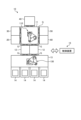
- FIG. 2 is a diagram showing an example of a film forming apparatus 20.
- a film forming apparatus 50 has the same configuration as the film forming apparatus 20 illustrated in FIG. 2.
- the film forming apparatus 20 illustrated in FIG. 2 includes a chamber 201, a mounting table 202, a gas supply mechanism 203, an exhaust device 204, and a microwave introduction device 205.
- the chamber 201 accommodates a substrate W.
- the mounting table 202 mounts the substrate W.
- the gas supply mechanism 203 supplies gas into the chamber 201.
- the exhaust device 204 exhausts gas from the chamber 201.
- the microwave introduction device 205 generates microwaves for generating plasma in the chamber 201 and introduces microwaves into the chamber 201.
- the chamber 201 is formed from a metal material such as aluminum or an alloy thereof, has a generally cylindrical shape, and has a plate-shaped top wall portion 211 and bottom wall portion 213, and a side wall portion 212 connecting these.
- the microwave introduction device 205 is provided at the top of the chamber 201, and functions as a plasma generation means that introduces electromagnetic waves (microwaves) into the chamber 201 to generate plasma.
- the microwave introduction device 205 will be described in detail later.
- the top wall 211 has a number of openings into which the microwave radiation mechanism and gas introduction section of the microwave introduction device 205, described later, are fitted.
- the side wall 212 has an inlet/outlet 214 for loading/unloading the substrate W between the chamber 201 and a transfer chamber (not shown) adjacent to the chamber 201.
- the inlet/outlet 214 is opened and closed by a gate valve G.
- the bottom wall 213 is provided with an exhaust device 204.
- the exhaust device 204 is provided on an exhaust pipe 216 connected to the bottom wall 213, and includes a vacuum pump and a pressure control valve.
- the chamber 201 is evacuated through the exhaust pipe 216 by the vacuum pump of the exhaust device 204.
- the pressure inside the chamber 201 is controlled by a pressure control valve.
- the mounting table 202 is generally disk-shaped and made of ceramics such as aluminum nitride.
- the mounting table 202 is supported by a cylindrical support member 220 and a base member 221 made of ceramics such as aluminum nitride that extend upward from the center of the bottom of the chamber 201.
- a guide ring 281 for guiding the substrate W is provided on the outer edge of the mounting table 202.
- lifting pins (not shown) for raising and lowering the substrate W are provided so as to be able to protrude and retract from the upper surface of the mounting table 202.
- a resistance heating type heater 282 is embedded inside the mounting table 202, and this heater 282 heats the substrate W placed thereon via the mounting table 202 by being powered by a heater power supply 283.
- a thermocouple (not shown) is also inserted into the mounting table 202, and the heating temperature of the substrate W can be controlled to a predetermined temperature, for example, in the range of 200 to 1000°C, based on a signal from the thermocouple.
- an electrode 284 of approximately the same size as the substrate W is embedded above the heater 282 inside the mounting table 202, and a high frequency bias power supply 222 is electrically connected to this electrode 284. A high frequency bias for attracting ions is applied from this high frequency bias power supply 222 to the mounting table 202. Note that the high frequency bias power supply 222 may not be provided depending on the characteristics of the plasma processing.
- a plurality of gas introduction nozzles 223 are fitted into the openings formed in the ceiling wall 211 of the chamber 201.
- a gas supply mechanism 203 is connected to each gas introduction nozzle 223 via a gas supply pipe 291.
- the gas supply mechanism 203 is a supply source of processing gas.
- a mixed gas containing a rare gas and a carbon-containing gas is used as the processing gas.
- argon is used as the rare gas.
- a mixed gas containing a silicon-containing gas, a reactive gas, and a rare gas is used as the processing gas.
- a mixed gas containing a silicon-containing gas, a reactive gas, and a rare gas is used as the processing gas.
- silane (SiH4), dichlorosilane (DCS), etc. are used as the silicon-containing gas.
- nitrogen, ammonia, oxygen, etc. are used as the reactive gas.
- argon, helium, etc. are used as the rare gas.
- the gas supply mechanism 203 is provided with a valve and a flow rate controller for each gas type, and the flow rate of the gas is adjusted for each gas type.
- a hydrogen-containing gas such as hydrogen gas, may be added to the processing gas.
- the microwave introduction device 205 is provided above the chamber 201 and functions as a plasma generation means that introduces electromagnetic waves (microwaves) into the chamber 201 to generate plasma.
- the microwave introduction device 205 has a ceiling wall portion 211 of the chamber 201, a microwave output portion 230, and an antenna unit 240.
- the ceiling wall portion 211 functions as a top plate.
- the microwave output portion 230 generates microwaves and distributes the microwaves to multiple paths before outputting them.
- the antenna unit 240 radiates the microwaves output from the microwave output portion 230 to the chamber 201.
- the microwave output unit 230 has a microwave power supply, a microwave oscillator, an amplifier, and a distributor.
- the microwave oscillator is solid-state and oscillates microwaves at, for example, 860 MHz (e.g., PLL oscillation).
- the microwave frequency is not limited to 860 MHz, and frequencies in the range of 700 MHz to 10 GHz, such as 2.45 GHz, 8.35 GHz, 5.8 GHz, and 1.98 GHz, can be used.
- the amplifier amplifies the microwaves oscillated by the microwave oscillator.
- the distributor distributes the microwaves amplified by the amplifier to multiple paths. The distributor distributes the microwaves while matching the impedance of the input side and output side.
- the antenna unit 240 includes multiple antenna modules. Each of the multiple antenna modules introduces microwaves distributed by a distributor in the microwave output section 230 into the chamber 201.
- the multiple antenna modules all have the same configuration.
- Each antenna module has an amplifier section 242 that mainly amplifies and outputs the distributed microwaves, and a microwave radiation mechanism 243 that radiates the microwaves output from the amplifier section 242 into the chamber 201.
- the amplifier section 242 has a phase shifter, a variable gain amplifier, a main amplifier, and an isolator.
- the phase shifter changes the phase of the microwave.
- the variable gain amplifier adjusts the power level of the microwave input to the main amplifier.
- the main amplifier is configured as a solid-state amplifier.
- the isolator separates the reflected microwaves that are reflected by the antenna section of the microwave radiation mechanism 243 (described later) and head toward the main amplifier.
- the microwave radiation mechanisms 243 are provided on the ceiling wall 211, as shown in FIG. 2, for example.
- the microwave radiation mechanism 243 has a cylindrical outer conductor and an inner conductor arranged coaxially with the outer conductor within the outer conductor.
- the microwave radiation mechanism 243 has a coaxial tube having a microwave transmission path between the outer conductor and the inner conductor, and an antenna unit that radiates microwaves into the chamber 201.
- a microwave transmitting plate 263 is fitted into the ceiling wall 211 on the underside of the antenna unit, and its underside is exposed to the internal space of the chamber 201. The microwaves that have passed through the microwave transmitting plate 263 generate plasma in the space within the chamber 201.
- the microwave radiation mechanism 243 is an example of a plasma source.
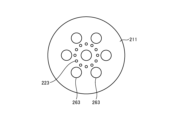
- FIG. 3 is a schematic diagram of an example of the top wall portion 211.
- seven microwave radiation mechanisms 243 are provided on the top wall portion 211, and the corresponding microwave transmission plates 263 are evenly arranged on the top wall portion 211 in a hexagonal close-packed arrangement. That is, one of the seven microwave transmission plates 263 is arranged approximately in the center of the top wall portion 211, and the other six microwave transmission plates 263 are arranged around it. These seven microwave transmission plates 263 are arranged so that the intervals between the adjacent microwave transmission plates 263 are even.
- the center of the top wall portion 211 is an example of a central region
- the periphery of the microwave radiation mechanism 243 arranged in the center of the top wall portion 211 is an example of a peripheral region. That is, one microwave radiation mechanism 243 is arranged in the central region, and six microwave radiation mechanisms 243 are arranged in the peripheral region.
- the multiple gas introduction nozzles 223 are arranged to surround the periphery of the central microwave transmission plate 263.
- the microwave radiation mechanism 243 arranged in the central region will be referred to as the central microwave radiation mechanism 243
- each of the microwave radiation mechanisms 243 arranged in the peripheral region will be referred to as the peripheral microwave radiation mechanisms 243.
- the number of microwave radiation mechanisms 243 is not limited to seven, and may be less than seven or more than seven.
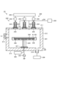
- [Configuration example of film forming apparatus 30] 4 is a diagram showing an example of a film forming apparatus 30.
- the film forming apparatus 30 includes a chamber 31, an exhaust mechanism 32, a gas supply unit 33, a shower head 35, and a stage 36.
- the film forming apparatus 30 is, for example, a chemical vapor deposition (CVD) apparatus.
- CVD chemical vapor deposition
- the exhaust mechanism 32 has a vacuum pump that exhausts the gas in the chamber 31, and a pressure adjustment valve that adjusts the pressure in the chamber 31.
- the inside of the chamber 31 is controlled by the exhaust mechanism 32 to a vacuum atmosphere of a predetermined pressure.
- a gas supply unit 33 that supplies multiple types of raw material monomers is connected to the chamber 31 via a shower head 35.
- the multiple types of raw material monomers are, for example, isocyanate and amine.
- Isocyanate is an example of a first monomer
- amine is an example of a second monomer.
- the gas supply unit 33 has a raw material supply source 330a, a raw material supply source 330b, a vaporizer 331a, and a vaporizer 331b.
- the raw material supply source 330a contains, for example, an isocyanate liquid.
- the raw material supply source 330b contains, for example, an amine liquid.
- the vaporizer 331a vaporizes the isocyanate liquid supplied from the raw material supply source 330a.
- the isocyanate vapor vaporized by the vaporizer 331a is introduced into the shower head 35 via the pipe 34a.
- the vaporizer 331b vaporizes the amine liquid supplied from the raw material supply source 330b.
- the amine vapor vaporized by the raw material supply source 330b is introduced into the shower head 35 via the pipe 34b.
- the shower head 35 is provided, for example, at the top of the chamber 31, and has a number of outlets formed on the bottom surface.
- the shower head 35 ejects the isocyanate vapor introduced via the pipe 34a and the amine vapor introduced via the pipe 34b in a shower-like manner from separate outlets into the chamber 31.
- a stage 36 is provided within the chamber 31.
- the stage 36 has a temperature control mechanism (not shown).
- a substrate W is placed on the stage 36, which is brought into the chamber 31 through an opening 31a formed in the side wall of the chamber 31.
- the opening 31a is opened and closed by a gate valve G.
- the stage 36 has a temperature control mechanism, which controls the temperature of the substrate W so that it becomes a temperature suitable for vapor deposition polymerization of the raw material monomer supplied from the gas supply unit 33.
- the temperature suitable for vapor deposition polymerization can be determined according to the type of raw material monomer.
- the temperature suitable for vapor deposition polymerization is, for example, within the range of 60°C to 100°C.
- a vapor deposition polymerization reaction of two types of raw material monomers occurs on the surface of the substrate W, forming an organic polymer film on the surface of the substrate W.
- the two types of raw material monomers are isocyanate and amine, an organic polymer film having polyurea bonds is formed on the surface of the substrate W.
- FIG. 5 is a diagram showing an example of a plasma processing apparatus 40.
- the plasma processing apparatus 40 has a chamber 41 formed of a conductive material.
- the chamber 41 is grounded.
- An exhaust mechanism 42 is connected to the chamber 41, and the gas inside the chamber 41 is exhausted by the exhaust mechanism 42, and the inside of the chamber 41 is controlled to a predetermined pressure.
- a stage 43 on which the substrate W is placed is provided in the chamber 41.
- the substrate W is placed on the stage 43 and is brought into the chamber 41 through an opening 41a formed in the side wall of the chamber 41.
- the opening 41a is opened and closed by a gate valve G.
- a heater 43a for heating the substrate W is provided in the stage 43.
- the stage 43 is electrically connected to the bottom of the chamber 41 and functions as an anode electrode.
- a shower head 44 is provided above the stage 43 so as to face the upper surface of the stage 43.
- the shower head 44 is supported on the upper part of the chamber 41 via an insulating member 44A.
- a power source 45 that supplies high-frequency power for generating plasma is connected to the shower head 44.
- the shower head 44 functions as a cathode electrode with respect to the stage 43.
- the gas supply source 46 supplies the process gas.
- the flow rate controller 47 adjusts the flow rate of the process gas supplied from the gas supply source 46 and supplies it into the diffusion space 44B of the shower head 44.
- the process gas supplied into the diffusion space 44B diffuses within the diffusion space 44B and is supplied in a shower-like manner into the chamber 41 from a plurality of outlets 44C formed on the lower surface of the diffusion space 44B.
- one gas supply source 46 and one flow rate controller 47 are shown in FIG. 5, in reality, a set of the gas supply source 46 and the flow rate controller 47 is provided for each type of gas used.
- the processing gas supplied into the chamber 41 through the shower head 44 is converted into plasma by high-frequency power supplied into the chamber 41 from the power source 45. Then, the ions and activated species contained in the plasma are used to perform processing such as etching on the substrate W.
- FIG. 6 is a diagram showing an example of a heating device 60.
- the heating device 60 has a chamber 61, an exhaust pipe 62, a supply pipe 63, a stage 64, and a lamp house 65.
- a lamp house 65 is provided at a position opposite the surface of the stage 64 on which the substrate W is placed.
- a lamp 65a such as an infrared lamp is disposed inside the lamp house 65.
- a gas supply unit 63a is connected to the side wall of the chamber 61 via a supply pipe 63.
- the gas supply unit 63a supplies an inert gas such as N2 gas into the chamber 61 via the supply pipe 63.
- An opening 61a for loading and unloading the substrate W is also formed in the side wall of the chamber 61.
- the opening 61a is opened and closed by a gate valve G.
- An exhaust device 66 is connected to the bottom of the chamber 61 via an exhaust pipe 62.
- the exhaust device 66 has a pressure adjustment valve.
- the exhaust device 66 exhausts the gas in the chamber 61 and controls the pressure adjustment valve so that the pressure inside the chamber 61 is set to a predetermined pressure.
- the lamp 65a can be turned on to heat the substrate W to a predetermined temperature in the inert gas atmosphere.
- FIG. 7 is a flowchart showing an example of a method for manufacturing a semiconductor device according to the first embodiment.
- the manufacturing method shown in Fig. 7 is realized by the control device 15 controlling each part of the manufacturing system 10.
- the following description will be given with reference to Figs. 8A to 8G.
- Step S100 is an example of process a).
- the substrate W having a structure such as that shown in FIG. 8A is loaded into the plasma processing apparatus 200 by the transfer robot 110 in the VTM 11.
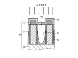
- the substrate W has a pattern including a plurality of metal-containing layers 71 formed on the underlayer 70 and a dielectric layer 72 formed on each of the metal-containing layers 71.
- a semiconductor device is manufactured from the substrate W.
- at least the surface of the underlayer 70 is formed of, for example, TiN or TaN.
- the metal-containing layer 71 contains at least one of, for example, Ru, Co, Cu, Mo, Ni, or W.
- the metal-containing layer 71 is used, for example, as wiring in the semiconductor device.
- the dielectric layer 72 is, for example, a silicon-containing film such as a silicon nitride film.
- Step S101 is an example of process b).
- a modifying gas is supplied into the chamber 201 to modify the sidewalls of the metal-containing layers 71.
- the pretreatment is performed by the film forming apparatus 20 under the following processing conditions, for example.
- Pressure in chamber 201 50 mTorr to 1 Torr (6.7 to 133 Pa)
- Temperature of substrate W 250 to 550° C. Processing time: 5 seconds to 15 minutes
- the pretreatment in step S101 reduces an oxide film that was unintentionally formed on the surface of the sidewall of the metal-containing layer 71 during transportation of the substrate W, etc.
- the modifying gas used in the pretreatment in step S101 includes an inert gas and a hydrogen-containing gas.
- the inert gas includes at least one of a rare gas such as He gas or Ar gas, or N2 gas
- the hydrogen-containing gas includes at least one of H2 gas or NH3 gas.
- plasma may be used in the pretreatment in step S101.
- the pretreatment using plasma is performed under the following processing conditions, for example.
- Pressure in chamber 201 50 mTorr to 1 Torr (6.7 to 133 Pa)
- Flow rate of hydrogen-containing gas e.g., H2 gas
- Microwave power 100-1500W
- Temperature of substrate W 250 to 550° C.
- Processing time 5 seconds to 15 minutes
- Step S102 is an example of process c).
- plasma is generated from a first process gas containing a carbon-containing gas in the chamber 201, and the graphene film 73 is formed on the side wall of the metal-containing layer 71 by using the generated plasma.
- the graphene film 73 is formed by the film formation apparatus 20 under the following process conditions, for example.
- a graphene film 73 is formed on the sidewall of the metal-containing layer 71, as shown in FIG. 8B, for example.
- the pressure in the chamber 201 is more preferably 50 mTorr to 100 mTorr (6.67 Pa to 13.3 Pa).
- the microwave power is more preferably 300 W to 1500 W.
- the first process gas includes a carbon-containing gas and an inert gas.
- the first process gas may include a hydrogen-containing gas such as H2 gas or NH3 gas.
- the carbon-containing gas is a hydrocarbon gas (e.g., C2H2 gas or C2H4 gas) represented by CxHy (x and y are natural numbers), and the inert gas is a rare gas such as He gas or Ar gas.
- a hydrocarbon gas e.g., C2H2 gas or C2H4 gas
- CxHy x and y are natural numbers
- the inert gas is a rare gas such as He gas or Ar gas.
- step S103 the substrate W is transported from the film forming apparatus 20 to the film forming apparatus 30 (step S103).
- step S103 the substrate W is transported out of the chamber 201 of the film forming apparatus 20 by the transport robot 110 in the VTM 11 and is transported into the chamber 31 of the film forming apparatus 30.
- Step S104 is an example of process d).
- a first monomer and a second monomer are supplied into the chamber 31, and a vapor deposition polymerization reaction of the first monomer and the second monomer occurs on the surface of the substrate W, forming a thermally decomposable polymer organic film on the surface of the substrate W.
- the first monomer is, for example, an isocyanate
- the second monomer is, for example, an amine
- the polymer organic film has a polyurea bond.
- an organic film 74 is embedded in the groove formed by adjacent metal-containing layers 71, as shown in FIG. 8C, for example.
- step S104 an organic film 74 is formed on the surface of the substrate W under, for example, the following processing conditions.
- Pressure in chamber 31 0.5 to 20 Torr (66.7-2666Pa)
- Flow rate of isocyanate vapor 1 to 20 sccm (0.0017-0.034Pa ⁇ m 3 /s)
- Flow rate of amine vapor 1 to 20 sccm (0.0017-0.034Pa ⁇ m 3 /s)
- Temperature of substrate W 40 to 150° C.
- step S105 the substrate W is transported from the film forming apparatus 30 to the plasma processing apparatus 40 (step S105).
- step S105 the substrate W is removed from the chamber 31 of the film forming apparatus 30 by the transport robot 110 in the VTM 11 and is transported into the chamber 41 of the plasma processing apparatus 40.
- Step S106 is an example of process h).
- plasma is generated from the processing gas in the chamber 41.
- the unnecessary organic film 74 formed on the dielectric layer 72 is removed by the generated plasma, for example, as shown in FIG. 8D. In other words, the organic film 74 is removed so as to expose the dielectric layer 72.
- step S107 the substrate W is transported from the plasma processing device 40 to the film forming device 50 (step S107).
- step S107 the substrate W is removed from the chamber 41 of the plasma processing device 40 by the transport robot 110 in the VTM 11 and is transported into the chamber 201 of the film forming device 50.
- Step S108 is an example of process e).
- plasma is generated in the chamber 201 from a processing gas containing, for example, organic aminosilane.
- a sealing film 75 is formed on the organic film 74, as shown in FIG. 8E.
- the sealing film 75 is, for example, a silicon oxide film.
- the sealing film 75 may be another silicon-containing film, such as a silicon nitride film.
- the sealing film 75 is formed by the film forming apparatus 50 under, for example, the following processing conditions.
- step S109 the substrate W is transported from the film forming apparatus 50 to the heating apparatus 60 (step S109).
- step S109 the substrate W is transported out of the chamber 201 of the film forming apparatus 50 by the transport robot 110 in the VTM 11 and is transported into the chamber 61 of the heating apparatus 60.
- Step S110 is an example of process f).
- the substrate W is heated to pyrolyze the organic film 74, and the organic film 74 is detached through the sealing film 75.
- an air gap 74a is formed between the groove formed by the adjacent metal-containing layers 71 and the sealing film 75.
- step S111 the substrate W is transported from the heating device 60 to the film forming device 50 (step S111).
- step S111 the substrate W is removed from the chamber 61 of the heating device 60 by the transport robot 110 in the VTM 11, and is transported back into the chamber 201 of the film forming device 50.
- a protective film is formed on the sealing film 75 (step S112).
- plasma is generated in the chamber 201 from a process gas containing, for example, an organic aminosilane.
- a protective film 76 is formed on the sealing film 75, as shown in, for example, FIG. 8G.
- the protective film 76 is, for example, a silicon nitride film.
- the protective film 76 is formed by the film forming apparatus 50 under, for example, the following process conditions.
- step S113 the substrate W is removed from the film forming apparatus 50 (step S113). Then, the method for manufacturing a semiconductor device shown in this flowchart is completed.
- Fig. 9 is a diagram showing an example of the state of the air gap 74a for each thickness of the sealing film 75.
- the thickness of the sealing film 75 is thicker than 1.2 nm.
- the thickness of the sealing film 75 is 2.4 nm, as shown in FIG. 9, even after the substrate W is heated, the organic film 74 in the groove formed by the adjacent metal-containing layers 71 is not completely detached and remains. Therefore, it is preferable that the thickness of the sealing film 75 is thinner than 2.4 nm.
- the thickness of the sealing film 75 was 1.6 nm and 2.0 nm, as shown in FIG. 9, for example, no organic film 74 was observed in the groove formed by adjacent metal-containing layers 71. Furthermore, the sealing film 75 was not torn. Therefore, it is preferable that the thickness of the sealing film 75 is 1.2 nm or more and 2.0 nm or less.
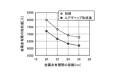
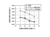
- the resistance value of the metal-containing layer 71 was measured when the air gap 74a was formed without forming the graphene film 73 on the side wall of the metal-containing layer 71, and the results shown in Fig. 10A and Fig. 10B were obtained.
- the metal-containing layer 71 was heated to remove the organic film 74, so that the crystal grains of the metal-containing layer 71 expanded, and the resistance value of the metal-containing layer 71 was reduced.
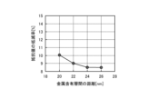
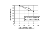
- the resistance value of the metal-containing layer 71 after the air gap 74a was formed was reduced by about 9% from the initial state.
- the reduction rate of the resistance value of the metal-containing layer 71 is increased by about 5% compared to the case where the graphene film 73 is not formed on the sidewall of the metal-containing layer 71. Therefore, in this embodiment, by forming the graphene film 73 on the sidewall of the metal-containing layer 71, the resistance value of the metal-containing layer 71 used as wiring in a semiconductor device can be further reduced.
- FIG. 12A is a diagram showing an example of the capacitance between metal-containing layers 71 in the comparative example.
- FIG. 12B is a diagram showing an example of the capacitance between metal-containing layers 71 in the first embodiment.
- the capacitance between the metal-containing layers 71 is almost unchanged between the initial state and after the air gap 74a is formed.
- the initial state as shown in FIG. 8A, for example, there is a space between adjacent metal-containing layers 71.
- the resistance value of the metal-containing layer 71 can be reduced, and by forming an air gap 74a between adjacent metal-containing layers 71, the capacitance between the metal-containing layers 71 can be reduced. This makes it possible to reduce the delay of signals flowing through the metal-containing layer 71 used as wiring within a semiconductor device.
- the method for manufacturing a semiconductor device in the first embodiment includes steps a), b), c), d), e), and f).
- a substrate (substrate W) having a pattern including a plurality of metal-containing layers (metal-containing layers 71) formed on an underlayer (underlayer 70) and a dielectric layer (dielectric layer 72) formed on each of the metal-containing layers is prepared in a chamber (chamber 201).
- a modifying gas is supplied into the chamber to modify the sidewalls of each metal-containing layer.
- step c) plasma is generated from a first processing gas including a carbon-containing gas in the chamber, and a graphene film (graphene film 73) is formed on the sidewall of the metal-containing layer using the generated plasma.
- step d) a pyrolyzable organic film (organic film 74) is embedded in a groove formed by adjacent metal-containing layers.
- step e) a sealing film (sealing film 75) is formed on the organic film embedded in the groove.
- step f) the substrate is heated to thermally decompose the organic film, and the organic film is detached through the sealing film, forming an air gap (air gap 74a) between the groove and the sealing film. This makes it possible to manufacture a semiconductor device with little signal delay.
- the method for manufacturing a semiconductor device in the first embodiment described above further includes a step of removing the organic film formed on the dielectric layer, which is performed between steps d) and e). This allows an air gap of a desired shape to be formed between adjacent metal-containing layers 71.
- the thickness of the sealing film is preferably 1.6 nm or more and 2.0 nm or less. This allows an air gap of the desired shape to be formed between adjacent metal-containing layers 71.
- the sealing film may be a silicon oxide film or a silicon nitride film. This makes it possible to remove the organic film embedded between adjacent metal-containing layers 71.
- the modifying gas contains an inert gas and a hydrogen-containing gas, and the flow rate ratio of the inert gas to the hydrogen-containing gas is preferably in the range of 200:2 to 50:50. This makes it possible to modify the sidewall of the metal-containing layer 71 so that the graphene film can be more easily attached.
- the inert gas contained in the modifying gas contains at least one of He gas, Ar gas, and N2 gas.
- the hydrogen-containing gas contained in the modifying gas contains at least one of H2 gas and NH3 gas. This makes it possible to modify the sidewall of the metal-containing layer 71 so that the graphene film can be easily attached.
- the temperature of the substrate in step c) is preferably 250° C. or higher and 550° C. or lower. This allows the graphene film to be efficiently formed on the sidewall of the metal-containing layer 71.
- the temperature of the substrate in step d) is preferably 40° C. or higher and 150° C. or lower. This allows the organic film to be efficiently embedded in the grooves formed by adjacent metal-containing layers.
- the temperature of the substrate in step e) is preferably 20°C or higher and 100°C or lower. This allows the sealing film to be efficiently formed on the organic film.
- the temperature of the substrate in step f) is preferably 350°C or higher and 450°C or lower. This allows the organic film to be efficiently detached through the sealing film.
- the surface of the underlayer is TiN or TaN. This makes it possible to suppress the formation of a graphene film on the underlayer.
- the metal-containing layer contains at least one of Ru, Co, and Cu. This allows a graphene film to be efficiently formed on the metal-containing layer.
- step d gases of the first monomer and the second monomer are supplied into the chamber, and the organic film is embedded in the groove by vapor deposition polymerization of the first monomer and the second monomer. This allows the organic film to be embedded efficiently in the groove formed by adjacent metal-containing layers.
- the first monomer is an isocyanate
- the second monomer is an amine
- the organic film contains a urea bond. This allows the organic film to be efficiently detached through the sealing film.
- the first embodiment described above is a semiconductor device manufacturing system (manufacturing system 10) that includes a first processing device (film forming device 20), a second processing device (film forming device 30), a third processing device (film forming device 50), a fourth processing device (heating device 60), and a control device (control device 15) that controls the first processing device, the second processing device, the third processing device, and the fourth processing device.
- the control device executes steps a), b), c), d), e), and f).
- a substrate (substrate W) having a pattern including a plurality of metal-containing layers (metal-containing layers 71) formed on an underlayer (underlayer 70) and a dielectric layer (dielectric layer 72) formed on each of the metal-containing layers is prepared in a chamber (chamber 201) of the first processing device.
- a modifying gas is supplied into the chamber to modify the sidewalls of each metal-containing layer.
- plasma is generated from a first processing gas containing a carbon-containing gas in the chamber, and the generated plasma is used to form a graphene film (graphene film 73) on the side wall of the metal-containing layer.
- a thermally decomposable organic film (organic film 74) is embedded in a groove formed by adjacent metal-containing layers using a second processing device.
- a sealing film (sealing film 75) is formed on the organic film embedded in the groove using a third processing device.
- an air gap (air gap 74a) is formed between the groove and the sealing film by thermally decomposing the organic film by heating the substrate using a fourth processing device, and detaching the organic film through the sealing film. This allows the manufacture of a semiconductor device with little signal delay.
- the organic film 74 in the groove formed by the adjacent metal-containing layers 71 may not be completely removed and may remain as a residue.
- the residue in the groove may become conductive due to heating. Therefore, the leakage current after the air gap 74a is formed may be larger than the leakage current at the stage where the graphene film 73 is formed, as shown in FIG. 13, for example. Therefore, in the second embodiment, in order to remove the residue after the air gap 74a is formed, a process for removing the organic film 74 is performed after the substrate W is heated to form the air gap 74a.
- Fig. 14 is a flowchart showing an example of a method for manufacturing a semiconductor device according to the second embodiment.
- the manufacturing method shown in Fig. 14 is realized by a control device 15 controlling each part of the manufacturing system 10.
- the processes in Fig. 14 denoted by the same reference numerals as those in Fig. 7 are the same as those described using Fig. 7 except for the points described below, and therefore will not be described again.
- step S120 the substrate W is transported from the heating device 60 to the plasma processing device 40 (step S120).
- step S120 the substrate W is transported by the transport robot 110 in the VTM 11 out of the chamber 61 of the heating device 60 and into the chamber 41 of the plasma processing device 40.
- Step S121 is an example of process g).
- plasma is generated from a processing gas in the chamber 41.
- the processing gas is Ar gas.
- the processing gas used in step S121 is an example of a third processing gas that does not contain oxygen. Note that the processing gas used in step S121 may be a rare gas other than Ar, or may be a gas that contains at least one of a rare gas, N2 gas, or H2 gas.
- step S121 plasma is generated under the following processing conditions, for example.
- Pressure in chamber 41 0.5 to 5 Torr (66.7-667Pa)
- Processing gas: Ar 200 to 2000 sccm (0.34-3.4Pa ⁇ m 3 /s)
- High frequency power 50-500W
- Temperature of substrate W 300 to 400° C.
- the generated plasma is irradiated onto the substrate W.
- This causes active species contained in the plasma to be supplied to the residue 77 remaining in the air gap 74a, decomposing the residue 77.
- the decomposed residue 77 is detached through the sealing film 75.
- step S122 the substrate W is transported from the plasma processing device 40 to the film forming device 50 (step S122).
- step S122 the substrate W is removed from the chamber 41 of the plasma processing device 40 by the transport robot 110 in the VTM 11 and is transported into the chamber 201 of the film forming device 50. Then, the processes from step S112 onwards are performed.
- FIG. 16 is a diagram showing an example of leakage current in the second embodiment.
- the leakage current when plasma is applied after the air gap 74a is formed is reduced compared to before the plasma is applied, as shown in FIG. 16 for example. Therefore, by applying plasma after the air gap 74a is formed, the leakage current between adjacent metal-containing layers 71 can be reduced.
- the method for manufacturing a semiconductor device in the second embodiment further includes step g).
- step g) after the air gap is formed in step f), plasma is irradiated into the groove through the sealing film. This makes it possible to reduce the leakage current between adjacent metal-containing layers 71.
- step g) of the second embodiment described above plasma generated from a third process gas that does not contain oxygen is irradiated into the groove through the sealing film.
- the third process gas contains at least one of a rare gas, N2 gas, and H2 gas. This makes it possible to reduce the leakage current between adjacent metal-containing layers 71.
- the substrate W is irradiated with plasma generated from a processing gas that does not contain oxygen, but the disclosed technology is not limited to this.
- the substrate W may be irradiated with plasma generated from a processing gas that contains oxygen. This makes it possible to more efficiently remove the residue 77 remaining in the air gap 74a.
- the graphene film 73 may also be removed due to active species derived from oxygen contained in the plasma, depending on the conditions. Furthermore, the sidewall of the metal-containing layer 71 may be oxidized due to active species derived from oxygen contained in the plasma, depending on the conditions, and the resistance value of the metal-containing layer 71 may increase. Therefore, when plasma generated from a processing gas containing oxygen is used to remove the residue 77, it is preferable to perform the processing under the following processing conditions.
- the graphene film 73 is formed using a film forming apparatus 20 having multiple microwave radiation mechanisms 543, but the disclosed technology is not limited to this.
- the graphene film 73 may be formed using a film forming apparatus having, for example, one microwave radiation mechanism.
- the deposition apparatus 20 that deposits the graphene film 73 using microwave plasma as the plasma source has been described as an example, but the disclosed technology is not limited to this.
- the plasma source is not limited to microwave plasma, and any plasma source can be used, such as capacitively coupled plasma, inductively coupled plasma, magnetron plasma, etc.
- an organic film 74 of a thermally decomposable polymer having a urea bond (-NH-CO-NH-) is formed on the surface of the substrate W using an isocyanate as the first monomer and an amine as the second monomer, but the disclosed technology is not limited to this.
- an organic film of a thermally decomposable polymer having a 2-aminoethanol bond (-NH-CH2-CH(OH)-) may be formed on the surface of the substrate W using an epoxide as the first monomer and an amine as the second monomer.
- an organic film of a thermally decomposable polymer having a urethane bond may be formed on the surface of the substrate W using an isocyanate as the first monomer and an alcohol as the second monomer.
- an organic film of a thermally decomposable polymer having an amide bond may be formed on the surface of the substrate W using an acyl halide as the first monomer and an amine as the second monomer.
- a carboxylic acid anhydride may be used as the first monomer and an amine as the second monomer to form an organic film of a thermally decomposable polymer having imide bonds (-CO-N(-)-CO-) on the surface of the substrate W.
- (Appendix 1) a) providing a substrate in a chamber having a pattern including a plurality of metal-containing layers formed on an underlayer and a dielectric layer formed on each of the metal-containing layers; b) modifying a sidewall of each of the metal-containing layers by supplying a modification gas into the chamber; c) generating a plasma from a first process gas including a carbon-containing gas in the chamber, and forming a graphene film on the sidewall of the metal-containing layer using the generated plasma; d) filling grooves formed by adjacent metal-containing layers with a thermally decomposable organic film; e) forming a sealing film on the organic film embedded in the groove; f) heating the substrate to thermally decompose the organic film and detach the organic film through the sealing film, thereby forming an air gap between the groove and the sealing film.
- a flow rate ratio of the inert gas to the hydrogen-containing gas is in a range of 200:2 to 50:50.
- Appendix 11 11.
- Appendix 12 12.
- Appendix 13 13.
- the method for manufacturing a semiconductor device according to claim 1, wherein the temperature of the substrate in the step c) is 250° C. or higher and 550° C. or lower.
- Appendix 14 14.
- (Appendix 17) 17 17. The method for manufacturing a semiconductor device according to claim 1, wherein a surface of the underlayer is TiN or TaN. (Appendix 18) 18.
- Appendix 19 19. The method for manufacturing a semiconductor device according to any one of appendixes 1 to 18, wherein in the step d), gases of a first monomer and a second monomer are supplied into the chamber, and the organic film is embedded in the groove by vapor deposition polymerization of the first monomer and the second monomer.
- the first monomer is an isocyanate; the second monomer is an amine; 20.
- the control device includes: a) providing a substrate having a pattern including a plurality of metal-containing layers formed on an underlayer and a dielectric layer formed on each of the metal-containing layers in a chamber of the first processing apparatus; b) modifying a sidewall of each of the metal-containing layers by supplying a modification gas into the chamber; c) generating a plasma from a first process gas including a carbon-containing gas in the chamber, and forming a graphene film on the sidewall of the metal-containing layer using the generated plasma; d) filling grooves formed by adjacent metal-containing layers with a thermally decomposable organic film using the second processing apparatus; e) forming a sealing film on the organic film embedded in the groove by using the third processing apparatus; f) using the fourth processing apparatus, heating the substrate
Landscapes
- Engineering & Computer Science (AREA)
- Physics & Mathematics (AREA)
- Condensed Matter Physics & Semiconductors (AREA)
- General Physics & Mathematics (AREA)
- Manufacturing & Machinery (AREA)
- Computer Hardware Design (AREA)
- Microelectronics & Electronic Packaging (AREA)
- Power Engineering (AREA)
- Chemical Vapour Deposition (AREA)
- Formation Of Insulating Films (AREA)
- Internal Circuitry In Semiconductor Integrated Circuit Devices (AREA)
Abstract
Un procédé de production d'un dispositif à semi-conducteur selon la présente invention comprend les étapes a), b), c), d), e) et f). L'étape a) consiste à préparer un substrat dans une chambre, le substrat ayant un motif qui comprend : une pluralité de couches contenant du métal qui sont formées sur une couche de base; et des couches diélectriques qui sont respectivement formées sur les couches contenant du métal. L'étape b) consiste à amener un gaz de modification dans la chambre et modifier une paroi latérale de chacune des couches contenant du métal. L'étape c) consiste à utiliser un plasma généré à l'intérieur de la chambre à partir d'un premier gaz de traitement qui comprend un gaz contenant du carbone pour former un film de graphène sur les parois latérales des couches contenant du métal. L'étape d) consiste à incorporer un film organique thermiquement décomposable dans des rainures formées par des couches adjacentes contenant du métal. L'étape e) consiste à former un film d'étanchéité sur le film organique incorporé dans les rainures. L'étape f) consiste à chauffer le substrat pour décomposer thermiquement le film organique, retirer le film organique au moyen du film d'étanchéité, et former un entrefer entre les rainures et le film d'étanchéité.
Applications Claiming Priority (2)
| Application Number | Priority Date | Filing Date | Title |
|---|---|---|---|
| JP2023197076A JP2025083615A (ja) | 2023-11-21 | 2023-11-21 | 半導体装置の製造方法および製造システム |
| JP2023-197076 | 2023-11-21 |
Publications (1)
| Publication Number | Publication Date |
|---|---|
| WO2025110012A1 true WO2025110012A1 (fr) | 2025-05-30 |
Family
ID=95826551
Family Applications (1)
| Application Number | Title | Priority Date | Filing Date |
|---|---|---|---|
| PCT/JP2024/039542 Pending WO2025110012A1 (fr) | 2023-11-21 | 2024-11-07 | Procédé de production et système de production de dispositif à semi-conducteur |
Country Status (2)
| Country | Link |
|---|---|
| JP (1) | JP2025083615A (fr) |
| WO (1) | WO2025110012A1 (fr) |
Citations (4)
| Publication number | Priority date | Publication date | Assignee | Title |
|---|---|---|---|---|
| US20140175656A1 (en) * | 2012-07-18 | 2014-06-26 | International Business Machines Corporation | Use of graphene to limit copper surface oxidation, diffusion and electromigration in interconnect structures |
| JP2021108353A (ja) * | 2019-12-27 | 2021-07-29 | 東京エレクトロン株式会社 | 半導体装置の製造方法および半導体装置の製造システム |
| JP2021114524A (ja) * | 2020-01-17 | 2021-08-05 | 東京エレクトロン株式会社 | エアギャップ形成方法 |
| US20220013467A1 (en) * | 2020-07-13 | 2022-01-13 | Samsung Electronics Co., Ltd. | Semiconductor device and method for fabricating thereof |
-
2023
- 2023-11-21 JP JP2023197076A patent/JP2025083615A/ja active Pending
-
2024
- 2024-11-07 WO PCT/JP2024/039542 patent/WO2025110012A1/fr active Pending
Patent Citations (4)
| Publication number | Priority date | Publication date | Assignee | Title |
|---|---|---|---|---|
| US20140175656A1 (en) * | 2012-07-18 | 2014-06-26 | International Business Machines Corporation | Use of graphene to limit copper surface oxidation, diffusion and electromigration in interconnect structures |
| JP2021108353A (ja) * | 2019-12-27 | 2021-07-29 | 東京エレクトロン株式会社 | 半導体装置の製造方法および半導体装置の製造システム |
| JP2021114524A (ja) * | 2020-01-17 | 2021-08-05 | 東京エレクトロン株式会社 | エアギャップ形成方法 |
| US20220013467A1 (en) * | 2020-07-13 | 2022-01-13 | Samsung Electronics Co., Ltd. | Semiconductor device and method for fabricating thereof |
Also Published As
| Publication number | Publication date |
|---|---|
| JP2025083615A (ja) | 2025-06-02 |
Similar Documents
| Publication | Publication Date | Title |
|---|---|---|
| JP4853857B2 (ja) | 基板の処理方法,コンピュータ読み取り可能な記録媒体及び基板処理装置 | |
| JP7422540B2 (ja) | 成膜方法および成膜装置 | |
| US20110045676A1 (en) | Remote plasma source seasoning | |
| TW201942053A (zh) | 形成石墨烯構造體的方法及裝置 | |
| US12018375B2 (en) | Flim forming method of carbon-containing film by microwave plasma | |
| US20210202298A1 (en) | Semiconductor device manufacturing method and semiconductor device manufacturing system | |
| KR101321155B1 (ko) | 실리콘 산화막용 성막 원료 및 그것을 이용한 실리콘 산화막의 성막 방법 | |
| US20250191907A1 (en) | Film forming method and film forming apparatus | |
| US20240120183A1 (en) | Substrate processing method and substrate processing apparatus | |
| JP2021100093A (ja) | エッチング方法、基板処理装置、及び基板処理システム | |
| US12486570B2 (en) | Film forming method and film forming apparatus | |
| WO2025110012A1 (fr) | Procédé de production et système de production de dispositif à semi-conducteur | |
| KR20210097044A (ko) | 에칭 방법, 기판 처리 장치, 및 기판 처리 시스템 | |
| US20230420294A1 (en) | Substrate processing method and substrate processing apparatus | |
| US20250210344A1 (en) | Semiconductor device manufacturing method and semiconductor device manufacturing system | |
| TW202538868A (zh) | 半導體裝置之製造方法及製造系統 | |
| US20250389018A1 (en) | Silicon carbonitride film-forming method and plasma processing apparatus | |
| KR100685826B1 (ko) | 증착 장치 및 이를 이용한 증착 방법 | |
| JP2024163650A (ja) | 基板処理方法および基板処理装置 | |
| JP2025112370A (ja) | 半導体装置の製造方法および製造システム | |
| WO2025197037A1 (fr) | Procédé de traitement de substrat et système de traitement de substrat | |
| TW202538869A (zh) | 半導體裝置之製造方法及製造系統 | |
| JP2025025811A (ja) | 成膜方法および成膜システム | |
| US20210272840A1 (en) | Method of manufacturing semiconductor device | |
| JP2024062790A (ja) | 基板処理方法及び基板処理システム |
Legal Events
| Date | Code | Title | Description |
|---|---|---|---|
| 121 | Ep: the epo has been informed by wipo that ep was designated in this application |
Ref document number: 24894004 Country of ref document: EP Kind code of ref document: A1 |