WO2024029311A1 - 複合材料、ヒートスプレッダ及び半導体パッケージ - Google Patents
複合材料、ヒートスプレッダ及び半導体パッケージ Download PDFInfo
- Publication number
- WO2024029311A1 WO2024029311A1 PCT/JP2023/025926 JP2023025926W WO2024029311A1 WO 2024029311 A1 WO2024029311 A1 WO 2024029311A1 JP 2023025926 W JP2023025926 W JP 2023025926W WO 2024029311 A1 WO2024029311 A1 WO 2024029311A1
- Authority
- WO
- WIPO (PCT)
- Prior art keywords
- composite material
- thickness direction
- layer
- less
- molybdenum
- Prior art date
- Legal status (The legal status is an assumption and is not a legal conclusion. Google has not performed a legal analysis and makes no representation as to the accuracy of the status listed.)
- Ceased
Links
Images




Classifications
-
- B—PERFORMING OPERATIONS; TRANSPORTING
- B32—LAYERED PRODUCTS
- B32B—LAYERED PRODUCTS, i.e. PRODUCTS BUILT-UP OF STRATA OF FLAT OR NON-FLAT, e.g. CELLULAR OR HONEYCOMB, FORM
- B32B15/00—Layered products comprising a layer of metal
- B32B15/01—Layered products comprising a layer of metal all layers being exclusively metallic
-
- H—ELECTRICITY
- H05—ELECTRIC TECHNIQUES NOT OTHERWISE PROVIDED FOR
- H05K—PRINTED CIRCUITS; CASINGS OR CONSTRUCTIONAL DETAILS OF ELECTRIC APPARATUS; MANUFACTURE OF ASSEMBLAGES OF ELECTRICAL COMPONENTS
- H05K7/00—Constructional details common to different types of electric apparatus
- H05K7/20—Modifications to facilitate cooling, ventilating, or heating
-
- H—ELECTRICITY
- H10—SEMICONDUCTOR DEVICES; ELECTRIC SOLID-STATE DEVICES NOT OTHERWISE PROVIDED FOR
- H10W—GENERIC PACKAGES, INTERCONNECTIONS, CONNECTORS OR OTHER CONSTRUCTIONAL DETAILS OF DEVICES COVERED BY CLASS H10
- H10W20/00—Interconnections in chips, wafers or substrates
- H10W20/40—Interconnections external to wafers or substrates, e.g. back-end-of-line [BEOL] metallisations or vias connecting to gate electrodes
- H10W20/41—Interconnections external to wafers or substrates, e.g. back-end-of-line [BEOL] metallisations or vias connecting to gate electrodes characterised by their conductive parts
- H10W20/44—Conductive materials thereof
- H10W20/4403—Conductive materials thereof based on metals, e.g. alloys, metal silicides
- H10W20/4421—Conductive materials thereof based on metals, e.g. alloys, metal silicides the principal metal being copper
-
- H—ELECTRICITY
- H10—SEMICONDUCTOR DEVICES; ELECTRIC SOLID-STATE DEVICES NOT OTHERWISE PROVIDED FOR
- H10W—GENERIC PACKAGES, INTERCONNECTIONS, CONNECTORS OR OTHER CONSTRUCTIONAL DETAILS OF DEVICES COVERED BY CLASS H10
- H10W40/00—Arrangements for thermal protection or thermal control
- H10W40/20—Arrangements for cooling
- H10W40/22—Arrangements for cooling characterised by their shape, e.g. having conical or cylindrical projections
-
- H—ELECTRICITY
- H10—SEMICONDUCTOR DEVICES; ELECTRIC SOLID-STATE DEVICES NOT OTHERWISE PROVIDED FOR
- H10W—GENERIC PACKAGES, INTERCONNECTIONS, CONNECTORS OR OTHER CONSTRUCTIONAL DETAILS OF DEVICES COVERED BY CLASS H10
- H10W40/00—Arrangements for thermal protection or thermal control
- H10W40/20—Arrangements for cooling
- H10W40/22—Arrangements for cooling characterised by their shape, e.g. having conical or cylindrical projections
- H10W40/226—Arrangements for cooling characterised by their shape, e.g. having conical or cylindrical projections characterised by projecting parts, e.g. fins to increase surface area
-
- H—ELECTRICITY
- H10—SEMICONDUCTOR DEVICES; ELECTRIC SOLID-STATE DEVICES NOT OTHERWISE PROVIDED FOR
- H10W—GENERIC PACKAGES, INTERCONNECTIONS, CONNECTORS OR OTHER CONSTRUCTIONAL DETAILS OF DEVICES COVERED BY CLASS H10
- H10W40/00—Arrangements for thermal protection or thermal control
- H10W40/20—Arrangements for cooling
- H10W40/231—Arrangements for cooling characterised by their places of attachment or cooling paths
- H10W40/242—Arrangements for cooling characterised by their places of attachment or cooling paths comprising thermal conductors between chips and the and the arrangements for cooling, e.g. compliant heat-spreaders
-
- H—ELECTRICITY
- H10—SEMICONDUCTOR DEVICES; ELECTRIC SOLID-STATE DEVICES NOT OTHERWISE PROVIDED FOR
- H10W—GENERIC PACKAGES, INTERCONNECTIONS, CONNECTORS OR OTHER CONSTRUCTIONAL DETAILS OF DEVICES COVERED BY CLASS H10
- H10W40/00—Arrangements for thermal protection or thermal control
- H10W40/20—Arrangements for cooling
- H10W40/25—Arrangements for cooling characterised by their materials
- H10W40/255—Arrangements for cooling characterised by their materials having a laminate or multilayered structure, e.g. direct bond copper [DBC] ceramic substrates
-
- H—ELECTRICITY
- H10—SEMICONDUCTOR DEVICES; ELECTRIC SOLID-STATE DEVICES NOT OTHERWISE PROVIDED FOR
- H10W—GENERIC PACKAGES, INTERCONNECTIONS, CONNECTORS OR OTHER CONSTRUCTIONAL DETAILS OF DEVICES COVERED BY CLASS H10
- H10W40/00—Arrangements for thermal protection or thermal control
- H10W40/20—Arrangements for cooling
- H10W40/25—Arrangements for cooling characterised by their materials
- H10W40/258—Metallic materials
Definitions
- the present disclosure relates to composite materials, heat spreaders, and semiconductor packages.
- This application claims priority based on Japanese Patent Application No. 2022-124936, which is a Japanese patent application filed on August 4, 2022. All contents described in the Japanese patent application are incorporated herein by reference.
- Patent Document 1 International Publication No. 2022/030197 (Patent Document 1) describes a plate-shaped composite material.
- the composite material described in Patent Document 1 has a first surface and a second surface opposite to the first surface.
- the first surface and the second surface constitute end faces in the thickness direction (hereinafter referred to as "thickness direction") of the composite material described in Patent Document 1.
- the composite material described in Patent Document 1 has a plurality of first layers and a plurality of second layers.
- the first layer and the second layer are alternately stacked along the thickness direction so that the first layer is located on the first surface and the second surface.
- the first layer is a layer of metal material containing copper as a main component.
- the second layer includes a molybdenum plate and a copper filler.
- a plurality of openings are formed in the molybdenum plate. The opening passes through the molybdenum plate along the thickness direction.
- the openings are circular in plan view and arranged in a square lattice shape in plan view.
- a copper filler is placed inside the opening.
- the composite material of the present disclosure is plate-shaped and has a first surface and a second surface opposite to the first surface.
- the composite material includes a plurality of first layers and at least one second layer.
- the first surface and the second surface constitute end faces in the thickness direction of the composite material.
- the first layer and the second layer are alternately stacked along the thickness direction so that the first layer is located on the first surface and the second surface.
- the first layer is a layer of metal material containing copper as a main component.
- the second layer has a molybdenum plate and a copper filler. A plurality of openings are formed in the molybdenum plate passing through the molybdenum plate along the thickness direction. A copper filler is placed inside the opening.
- the openings are arranged in a lattice arrangement.
- the opening has a first width in the row direction of the lattice arrangement and a second width in the column direction of the lattice arrangement orthogonal to the row direction.
- the first width is greater than 350 ⁇ m.
- the value obtained by dividing the second width by the first width is 1 or more and 2 or less.
- the molybdenum plate has a continuous portion along the first direction without interfering with the opening, and a portion interfering with the opening along the second direction different from the first direction. It has a continuous part without any difference.
- the angle between the first direction and the second direction is 47° or more and 90° or less.
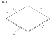
- FIG. 1 is a perspective view of a composite material 10.
- FIG. 2 is a sectional view taken along line II-II in FIG.
- FIG. 3 is a sectional view taken along line III-III in FIG.
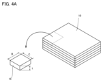
- FIG. 4A is a first explanatory diagram of a procedure for preparing a sample for measuring thermal conductivity in the thickness direction of the composite material 10.
- FIG. 4B is a second explanatory diagram of the procedure for preparing a sample for measuring thermal conductivity in the thickness direction of the composite material 10.
- FIG. 4C is a third explanatory diagram of the procedure for preparing a sample for measuring thermal conductivity in the thickness direction of the composite material 10.
- FIG. 5 is a manufacturing process diagram of the composite material 10.
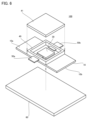
- FIG. 6 is an exploded perspective view of the semiconductor package 100.
- the present disclosure has been made in view of the problems of the prior art as described above. More specifically, the present disclosure provides a composite member that can reduce the anisotropy of the coefficient of linear expansion in a plane perpendicular to the thickness direction.
- the composite material according to the embodiment is plate-shaped and has a first surface and a second surface that is the opposite surface to the first surface.
- the composite material includes a plurality of first layers and at least one second layer.
- the first surface and the second surface constitute end faces in the thickness direction of the composite material.
- the first layer and the second layer are alternately stacked along the thickness direction so that the first layer is located on the first surface and the second surface.
- the first layer is a layer of metal material containing copper as a main component.
- the second layer has molybdenum plates and copper filler. A plurality of openings are formed in the molybdenum plate passing through the molybdenum plate along the thickness direction. A copper filler is placed inside the opening.
- the openings are arranged in a lattice arrangement.
- the opening has a first width in the row direction of the lattice arrangement and a second width in the column direction of the lattice arrangement orthogonal to the row direction.
- the first width is greater than 350 ⁇ m.
- the value obtained by dividing the second width by the first width is 1 or more and 2 or less.
- the molybdenum plate has a continuous portion along the first direction without interfering with the opening, and a portion interfering with the opening along the second direction different from the first direction. It has a continuous part without any difference.
- the angle between the first direction and the second direction is 47° or more and 90° or less.
- the angle between the first direction and the second direction may be less than 90°.
- the number of openings per 1 mm 2 may be less than 3 in a cross-sectional view perpendicular to the thickness direction.
- the number of openings per 1 mm 2 may be less than 2 in a cross-sectional view perpendicular to the thickness direction.
- the molybdenum plate may have an aperture ratio of 20 percent or more in a cross-sectional view orthogonal to the thickness direction.
- the volume ratio of molybdenum in the composite material may be 25% or less.
- the volume ratio of molybdenum in the composite material may be 15% or more. According to the composite material (7) above, the coefficient of linear expansion can be reduced.
- the volume ratio of molybdenum in the composite material may be less than 15%. According to the composite material (8) above, thermal conductivity can be increased.
- the total number of first layers and number of second layers may be five.
- the thickness of the composite material may be 1.5 mm or less.
- the thickness of the second layer may be 0.3 mm or less.
- the coefficient of linear expansion in the row direction when the temperature changes from room temperature to 800°C is the linear expansion coefficient in the column direction when the temperature changes from room temperature to 800°C.
- the value divided by the coefficient may be 1.5 or less.
- the pitch between adjacent openings in the column direction may be larger than the pitch between adjacent openings in the row direction.
- the heat spreader according to the embodiment includes the composite materials of (1) to (11) above.
- the first surface forms a contact surface with the heat generation source.
- a semiconductor package includes the composite material of (1) to (11) above and a semiconductor element.
- a semiconductor element is disposed on the first surface.
- the semiconductor package of (13) above may further include a case member made of a ceramic material.
- the case member may be placed on the first surface so as to surround the semiconductor element.
- the composite material according to the embodiment is referred to as a composite material 10.
- the semiconductor package according to the embodiment is referred to as a semiconductor package 100.
- FIG. 1 is a perspective view of the composite material 10. As shown in FIG. 1, the composite material 10 has a plate shape. The thickness direction of the composite material 10 is referred to as the "thickness direction.” Composite material 10 has a first surface 10a and a second surface 10b. The first surface 10a and the second surface 10b constitute end surfaces of the composite material 10 in the thickness direction. The second surface 10b is the opposite surface to the first surface 10a.
- FIG. 2 is a sectional view taken along II-II in FIG. 1.
- the composite material 10 has a plurality of first layers 11 and at least one second layer 12.
- the first layer 11 and the second layer 12 are laminated along the thickness direction so that the first layer 11 is located on the first surface 10a and the second surface 10b.
- Thickness T1 is preferably 1.5 mm or less.
- Thickness T2 is preferably 0.3 mm or less, more preferably 0.15 mm or less.
- the total number of first layers 11 and second layers 12 is 3 or more.
- the number of first layers 11 and the number of second layers 12 are preferably five.
- the first layer 11 is a layer of a metal material whose main component is copper.
- Metal material containing copper as a main component means a metal material having a copper content of 50% by mass or more.
- the first layer 11 is preferably a layer of a metal material having a copper content of 70% by mass or more.
- the first layer 11 is, for example, a layer of pure copper. Pure copper is a metal material consisting of copper and unavoidable impurities that make up the remainder.
- the second layer 12 includes a molybdenum plate 13 and a copper filler 14.
- the molybdenum plate 13 is a plate of a metal material whose main component is molybdenum. "Metal material containing molybdenum as a main component" means a metal material having a molybdenum content of 50% by mass or more.
- the molybdenum plate 13 is preferably a plate of a metal material having a molybdenum content of 70% by mass or more.
- the molybdenum plate 13 is, for example, a pure molybdenum plate. Pure molybdenum is a metal material consisting of molybdenum and the remaining unavoidable impurities.
- the copper filler 14 is made of the same material as the first layer 11, for example.
- FIG. 3 is a cross-sectional view taken along III-III in FIG. 2.
- the molybdenum plate 13 has a plurality of openings 13a formed therein.
- the opening 13a passes through the molybdenum plate 13 along the thickness direction.
- the openings 13a are arranged in a lattice arrangement. More specifically, in a cross-sectional view perpendicular to the thickness direction, the openings 13a are arranged in a houndstooth pattern.
- the openings 13a may be arranged in a square lattice shape or a rectangular lattice shape.
- the row direction and column direction of the lattice arrangement of the openings 13a are referred to as the "row direction” and the “column direction", respectively.
- the column direction is, for example, along the rolling direction of the composite material 10.
- the column direction is orthogonal to the row direction.
- the pitch between adjacent openings 13a in the row direction is defined as a first pitch.
- the pitch between adjacent openings 13a in the column direction is defined as a second pitch.
- the second pitch is larger than the first pitch.
- the first pitch and the second pitch are measured in a cross section passing through the center of the molybdenum plate 13 in the thickness direction and perpendicular to the thickness direction.
- a cross section passing through the center of the molybdenum plate 13 in the thickness direction and perpendicular to the thickness direction is exposed as follows.
- the distance between the first surface 10a and the center of the molybdenum plate 13 in the thickness direction is measured.
- the composite material 10 is polished from the first surface 10a side using a plane polisher or an automatic rotary polisher.
- the amount of polishing at this time is set to be equal to the distance between the first surface 10a and the center of the molybdenum plate 13 in the thickness direction, which was measured as described above. As a result, a cross section passing through the center of the molybdenum plate 13 in the thickness direction and perpendicular to the thickness direction is exposed.
- the first pitch is obtained by measuring the distance between the centers of adjacent openings 13a in the row direction for all openings 13a and dividing the sum of the measured values by the number of openings 13a.
- the second pitch is determined by measuring the distance between the centers of adjacent openings 13a in the column direction for all openings 13a, and dividing the sum of the measured values by the number of openings 13a. It is obtained by A digital microscope is used to measure the first pitch and the second pitch.
- the opening 13a has a first width W1, which is the width in the row direction, and a second width W2, which is the width in the column direction.
- the first width W1 and the second width W2 are measured in a cross section passing through the center of the molybdenum plate 13 in the thickness direction and perpendicular to the thickness direction.
- the first width W1 is obtained by measuring the width of all the openings 13a in the row direction and dividing the sum of the measured values by the number of openings 13a.
- the second width W2 is obtained by measuring the width of all the openings 13a in the column direction and dividing the measured value by the number of openings 13a.
- the first width W1 is greater than 350 ⁇ m.
- the value obtained by dividing the second width W2 by the first width W1 is greater than or equal to 1 and less than or equal to 2.
- a digital microscope is used to measure the first width W1 and the second width W2.
- the opening 13a In a cross-sectional view perpendicular to the thickness direction, the opening 13a has an elliptical shape, for example.
- the long axis of the ellipse is, for example, along the column direction.
- the opening 13a In a cross-sectional view perpendicular to the thickness direction, the opening 13a may be circular. However, the cross-sectional shape of the opening 13a is not limited to these.
- the number of openings 13a per 1 mm 2 is, for example, less than three.
- the number of openings 13a per 1 mm 2 is preferably less than two.
- the number of openings 13a per 1 mm 2 is the number of openings 13a in a cross section that passes through the center of the molybdenum plate 13 in the thickness direction and is perpendicular to the thickness direction, expressed as the area of the cross section (unit: mm 2 ). It is obtained by dividing.
- the aperture ratio of the molybdenum plate 13 is, for example, 20 percent or more.
- the aperture ratio of the molybdenum plate 13 may be 30% or more or 35% or more.
- the aperture ratio of the molybdenum plate 13 is, for example, 70% or less.
- the aperture ratio of the molybdenum plate 13 may be 60% or less.
- the aperture ratio of the molybdenum plate 13 is determined by measuring the total opening area of the apertures 13a in a cross section passing through the center of the molybdenum plate 13 in the thickness direction and orthogonal to the thickness direction, and calculating the total of the measured values. It is obtained by dividing by the area of the cross section.
- the opening area of the opening 13a in a cross section passing through the center of the molybdenum plate 13 in the thickness direction and perpendicular to the thickness direction is measured using a digital microscope.
- the molybdenum plate 13 has a continuous portion along the first direction without interfering with the opening 13a and a continuous portion along the second direction without interfering with the opening 13a. It has a continuous part.
- the first direction is the direction of straight line L1 in FIG. 3, and the second direction is the direction of straight line L2 in FIG.
- the first direction and the second direction may be different from the column direction and the row direction.
- the angle between the first direction and the second direction is defined as angle ⁇ .
- the angle ⁇ is the intersection angle of the straight line L1 and the straight line L2 that is less than or equal to 90°.
- the angle ⁇ is 47° or more and 90° or less.
- the angle ⁇ is preferably 47° or more and less than 90°.
- the angle ⁇ is measured in a cross section passing through the center of the molybdenum plate 13 in the thickness direction and perpendicular to the thickness direction.
- the one with the smallest angle ⁇ is selected from the three or more directions. shall be.
- the thermal conductivity of the composite material 10 in the thickness direction is preferably 270 W/m ⁇ K or more at room temperature.
- the thermal conductivity of the composite material 10 in the thickness direction is preferably 300 W/m ⁇ K or more at room temperature.
- Room temperature means 27°C.
- the thermal conductivity in the thickness direction of the composite material 10 is measured by using a laser flash method.
- the thermal diffusivity of the composite material 10 is measured using LFA447 MicroFlash (manufactured by NETZSCH), and the thermal diffusivity of the composite material 10 is measured based on the thermal diffusivity and the volume ratio and specific heat of each constituent material of the composite material 10.
- the thermal conductivity in the thickness direction of 10 is calculated.
- the specific heat of each constituent material is determined based on "Metal Data Book 4th Edition" edited by the Japan Institute of Metals (2004, Maruzen Publishing).
- the thermal conductivity of a pure copper sample having the same shape is measured under the same conditions, and the measurement results are corrected using the results as a reference.
- FIG. 4A is a first explanatory diagram of the procedure for preparing a sample for measuring thermal conductivity in the thickness direction of the composite material 10. As shown in FIG. 4A, a thin piece 15 is cut out from the composite material 10 to be measured. The thickness, length and width of the thin piece 15 are t (mm), B (mm) and C (mm), respectively.
- X be the number obtained by dividing 2 by t and rounding up the decimal places.
- the value obtained by dividing 10 by B and rounding up the decimal point is set as Y1.
- Y2 be the number obtained by dividing 10 by C and rounding up the decimal places.
- a number of thin pieces 15 equal to the product of X, Y1, and Y2 are cut out from the composite material 10 to be measured.
- FIG. 4B is a second explanatory diagram of the procedure for preparing a sample for measuring thermal conductivity in the thickness direction of the composite material 10.
- a block 16 is produced from X thin pieces 15.
- the thickness, length and width of the block 16 are approximately 2 (mm), B (mm) and C (mm), respectively.
- X pieces of thin pieces 15 are stacked.
- amorphous powder made of pure silver and having an average particle size of 4 ⁇ m is placed between adjacent thin pieces 15 .
- the amount of amorphous powder placed between adjacent flakes 15 is 0.2 g ⁇ 30 percent per 100 mm 2 .
- a rectangular mold (not shown) in which an opening with internal dimensions of B (mm) x C (mm) is formed is prepared, and the molds are stacked in the opening.
- a thin piece 15 is arranged.
- the above mold is made of graphite.
- the stacked flakes 15 are heat treated under a load P.
- the load P is 4.9N or more and 9.8N or less.
- the heat treatment is performed in an inert gas atmosphere.
- the heat treatment is performed at a holding temperature of 900° C. and a holding time of 10 minutes.
- the heat treatment softens and deforms the amorphous powder, and the adjacent thin pieces 15 are bonded together, thereby producing the block 16.
- FIG. 4C is a third explanatory diagram of the procedure for creating a sample for measuring thermal conductivity in the thickness direction of the composite material 10.
- a measurement sample 17 having a height of about 10 mm, a width of about 10 mm, and a thickness of about 2 mm is produced.
- the adhesive member used is one that can withstand temperatures up to about 800° C., such as silver solder foil or ceramic adhesive.
- the blocks 16 arranged vertically in Y1 blocks and horizontally in Y2 blocks may be fixed by wrapping stainless steel wire or the like around the outer periphery thereof.
- Linear expansion coefficient (first linear expansion coefficient) of the composite material 10 in the row direction when the temperature changes from room temperature to 800°C and linear expansion coefficient of the composite material 10 in the column direction when the temperature changes from room temperature to 800°C is preferably 14 ppm/K or less. It is more preferable that the first linear expansion coefficient and the second linear expansion coefficient are 10 ppm/K or less. The value obtained by dividing the first linear expansion coefficient by the second linear expansion coefficient is 1.5 or less.
- the first coefficient of linear expansion and the second coefficient of linear expansion are calculated by measuring the displacement of the composite material 10 in the row direction and column direction in the temperature range from room temperature to 800°C using TD5000SA (manufactured by Bruker AXS). Ru.
- TD5000SA manufactured by Bruker AXS
- Ru the planar shape of the composite material 10 is a rectangular shape of 3 mm x 15 mm. Measured values are averaged over three samples.
- the volume ratio of molybdenum in the composite material 10 is, for example, 25% or less. From the viewpoint of increasing the thermal conductivity in the thickness direction of the composite material 10, the volume ratio of molybdenum in the composite material 10 is preferably 15% or more. On the other hand, from the viewpoint of reducing the coefficient of linear expansion of the composite material 10, the volume ratio of molybdenum in the composite material 10 is preferably less than 15%.
- FIG. 5 is a manufacturing process diagram of the composite material 10.
- the method for manufacturing the composite material 10 includes a preparation step S1, a hole punching step S2, and a rolling step S3.
- a first plate material and a second plate material are prepared.
- the first plate material is a plate material made of a metal material whose main component is copper.
- the second plate material is a plate material made of a metal material containing molybdenum as a main component.
- drilling is performed on the second plate material.
- a plurality of openings are formed in the second plate material in the thickness direction.
- the second plate material becomes the molybdenum plate 13.
- the drilling process on the second plate material is performed, for example, by etching or laser irradiation.
- the laminate 20 is prepared.
- the laminate 20 is prepared by alternately arranging the first plates and the molybdenum plates 13 along the thickness direction of the laminate 20.
- the laminate 20 is subjected to heat treatment.
- the laminate 20 is heated to a predetermined temperature in a hydrogen atmosphere. This predetermined temperature is below the melting point of the first plate material and is a temperature at which the first plate material is sufficiently softened. This predetermined temperature is, for example, 900°C.
- the laminate 20 is passed through a rolling roller.
- the first plate material and the molybdenum plate 13 are joined to each other while being rolled.
- the first plate material fills the opening 13a of the molybdenum plate 13 and becomes the copper filler 14.
- the remainder of the first plate material that is not filled in the opening 13a becomes the first layer 11.
- the method for manufacturing the composite material 10 may further include a rolling step S4.
- the rolling process S4 is performed after the rolling process S3.
- the thickness T1 is adjusted by cold rolling the composite material 10.
- FIG. 6 is an exploded perspective view of the semiconductor package 100.
- the semiconductor package 100 includes a composite material 10, a semiconductor element 30, a case member 40, a lid 41, and terminals 50a and 50b.
- the composite material 10 functions as a heat spreader in the semiconductor package 100.
- Semiconductor element 30 is arranged on first surface 10a.
- a heat transfer member may be interposed between the semiconductor element 30 and the first surface 10a.
- the semiconductor element 30 becomes a heat source during operation.
- Case member 40 is made of, for example, a ceramic material.
- the ceramic material is, for example, alumina (Al 2 O 3 ).
- Case member 40 is arranged on first surface 10a so as to surround semiconductor element 30.
- the lower end (end on the first surface 10a side) of the case member 40 and the first surface 10a are joined by, for example, brazing.
- the lid 41 is made of, for example, a ceramic material or a metal material. The lid 41 closes off the upper end side of the case member 40.
- the terminal 50a and the terminal 50b are inserted into the case member 40. As a result, one end of the terminal 50a and the terminal 50b is located within the space defined by the first surface 10a, the case member 40, and the lid 41, and the other end of the terminal 50a and the terminal 50b is located outside the space. are doing.
- the terminal 50a and the terminal 50a are made of, for example, a metal material.
- the metal material is, for example, Kovar.
- one end side of the terminal 50a and the terminal 50b is electrically connected to the semiconductor element 30.
- the semiconductor package 100 is electrically connected to a device or circuit other than the semiconductor package 100 at the other end of the terminals 50a and 50b.
- a heat dissipation member 60 is attached to the second surface 10b.
- the heat dissipation member 60 is, for example, a metal plate in which a flow path through which a refrigerant flows is formed.
- the heat radiating member 60 is not limited to this.
- the heat radiation member 60 may be, for example, a cooling fin.
- a heat transfer member may be interposed between the heat radiation member 60 and the second surface 10b.
- the case member 40 is joined onto the composite material 10 by brazing or the like. Therefore, in order to reduce thermal stress caused by the difference between the coefficient of linear expansion of the composite material 10 and the coefficient of linear expansion of the case member 40, the coefficient of linear expansion of the composite material 10 and the coefficient of linear expansion of the case member 40 are preferably close to each other. preferable.
- the coefficient of linear expansion of the composite material 10 has anisotropy, even if the coefficient of linear expansion of the composite material 10 in a certain direction (for example, the column direction) is close to the coefficient of linear expansion of the case member 40, in another direction ( For example, the difference between the coefficient of linear expansion of the composite material 10 and the coefficient of linear expansion of the case member 40 in the row direction becomes large.
- the coefficient of linear expansion of molybdenum is smaller than that of copper, the coefficient of linear expansion of the composite material 10 becomes smaller in the direction in which the portion of the molybdenum plate 13 that is continuous without interfering with the opening 13a extends. Cheap. Therefore, as the angle ⁇ increases, the anisotropy of the linear expansion coefficient of the composite material 10 decreases. On the other hand, as the angle ⁇ becomes smaller, the distance between adjacent openings 13a becomes larger, and the molybdenum plate 13 becomes more likely to break between adjacent openings 13a during rolling.
- the semiconductor element that is the heat source Since the heat generated at 30 passes through the copper filler 14 more easily when passing through the second layer 12, the thermal resistance of the second layer 12 is reduced.
- the distance between adjacent openings 13a becomes short, the molybdenum plate 13 tends to break between adjacent openings 13a during rolling.
- the first width W1 is larger than 350 ⁇ m, and the second width W2 is divided by the first width W1. Even if the value is 1 or more and 2 or less, it is possible to reduce the anisotropy of the linear expansion coefficient of the composite material 10 while suppressing breakage of the molybdenum plate 13 between adjacent openings 13a. Do you get it.
- Samples 1 to 7 were prepared as composite material samples. As shown in Table 1, in samples 1 to 7, the angle ⁇ , the first width W1, the second width W2, the first pitch, the second pitch, the number of openings 13a per 1 mm 2 , and the molybdenum plate The aperture ratio of 13 was changed. In samples 1 to 7, the first layer 11 is a pure copper layer, and the molybdenum plate 13 is a pure molybdenum plate. In samples 1 to 7, the number of first layers 11 was three, and the number of second layers 12 was two.
- the thickness of the first plate material and the thickness of the molybdenum plate 13 before rolling were adjusted, and the rolling reduction rate during rolling was adjusted.
- the volume ratio of T1 and molybdenum was adjusted.
- the reduction rate during rolling was adjusted appropriately to prevent internal breakage of the material. Note that the thickness of the first plate shown in Table 2 is the thickness of the first plate on the outermost surface of the laminate 20.
- Condition A is that the angle ⁇ is 47° or more and 90° or less.
- Condition B is that the first width W1 is 350 ⁇ m or more.
- Condition C is that the value obtained by dividing the second width W2 by the first width W1 is greater than or equal to 1 and less than or equal to 2. In samples 1 to 4, all of conditions A to C were satisfied. On the other hand, in samples 5 to 7, at least one of conditions A to C was not satisfied.
- the first linear expansion coefficient, second linear expansion coefficient, and thermal conductivity in the thickness direction were measured. As shown in Table 3, in samples 1 to 4, the value obtained by dividing the first linear expansion coefficient by the second linear expansion coefficient was 1.5 or less. On the other hand, in samples 5 to 7, the value obtained by dividing the first linear expansion coefficient by the second linear expansion coefficient was larger than 1.5.
- the linear expansion coefficient of the composite material 10 can be reduced by making the volume ratio of molybdenum less than 15%, and the thermal conductivity of the composite material 10 can be reduced by making the volume ratio of molybdenum 15% or more. Experiments have shown that it can be made smaller.
Landscapes
- Engineering & Computer Science (AREA)
- Physics & Mathematics (AREA)
- Thermal Sciences (AREA)
- Microelectronics & Electronic Packaging (AREA)
- Cooling Or The Like Of Semiconductors Or Solid State Devices (AREA)
- Chemical & Material Sciences (AREA)
- Materials Engineering (AREA)
Abstract
Description
特許文献1に記載の複合材料では、開口部の開口径が小さいため、第2層の厚さ方向における熱伝導率に改善の余地がある。特許文献1に記載の複合材料において第2層の厚さ方向における熱伝導率を改善するために開口部の開口径を大きくすると、隣り合う2つの開口部の間の距離が小さくなり、隣り合う2つの開口部の間でモリブデン板に破損が生じることがある。このような破損を避けるために、開口部を例えば千鳥格子状に配置することが考えられる。しかしながら、開口部を千鳥格子状に配置すると、厚さ方向に直交する面内における線膨張係数の異方性が大きくなってしまうことがある。
本開示の複合材料によると、厚さ方向に直交する面内における線膨張係数の異方性を小さくすることが可能である。
まず、本開示の実施形態を列記して説明する。
次に、本開示の実施形態の詳細を、図面を参照しながら説明する。以下の図面では、同一又は相当する部分に同一の参照符号を付し、重複する説明は繰り返さないものとする。実施形態に係る複合材料を、複合材料10とする。実施形態に係る半導体パッケージを、半導体パッケージ100とする。
以下に、複合材料10の構成を説明する。
以下に、複合材料10の製造方法を説明する。
以下に、半導体パッケージ100の構成を説明する。
以下に、複合材料10の効果を説明する。
複合材料のサンプルとして、サンプル1からサンプル7が準備された。表1に示されているように、サンプル1からサンプル7では、角度θ、第1幅W1、第2幅W2、第1ピッチ、第2ピッチ、1mm2あたりの開口部13aの数及びモリブデン板13の開口率が変化された。サンプル1からサンプル7では、第1層11は純銅の層であり、モリブデン板13は純モリブデンの板である。サンプル1からサンプル7では、第1層11の数は3とされ、第2層12の数は2とされた。


Claims (14)
- 第1表面及び前記第1表面の反対面である第2表面を有する板状の複合材料であって、
前記複合材料は、複数の第1層と、少なくとも1つの第2層とを備え、
前記第1表面及び前記第2表面は、前記複合材料の厚さ方向における端面をなしており、
前記第1層及び前記第2層は、前記厚さ方向に沿って、前記第1層が前記第1表面及び前記第2表面に位置するように交互に積層されており、
前記第1層は、銅を主成分とする金属材料の層であり、
前記第2層は、モリブデン板と、銅フィラーとを有し、
前記モリブデン板には、前記厚さ方向に沿って前記モリブデン板を貫通している複数の開口部が形成されており、
前記銅フィラーは、前記開口部の内部に配置されており、
前記厚さ方向に直交する断面視において、前記開口部は、格子配列をなすように並んでおり、
前記厚さ方向に直交する断面視において、前記開口部は、前記格子配列の行方向において第1幅を有するとともに、前記行方向に直交している前記格子配列の列方向において第2幅を有し、
前記第1幅は、350μmよりも大きく、
前記第2幅を前記第1幅で除した値は、1以上2以下であり、
前記厚さ方向に直交する断面視において、前記モリブデン板は、第1方向に沿って前記開口部と干渉することなく連続している部分と、前記第1方向とは異なる第2方向に沿って前記開口部と干渉することなく連続している部分とを有し、
前記第1方向と前記第2方向とのなす角度は、47°以上90°以下である、複合材料。 - 前記第1方向と前記第2方向とのなす角度は、90°未満である、請求項1に記載の複合材料。
- 前記厚さ方向に直交する断面視において、1mm2あたりの前記開口部の数が3個未満である、請求項1又は請求項2に記載の複合材料。
- 前記厚さ方向に直交する断面視において、1mm2あたりの前記開口部の数が2個未満である、請求項1又は請求項2に記載の複合材料。
- 前記厚さ方向に直交する断面視において、前記モリブデン板の開口率が20パーセント以上である、請求項1から請求項4のいずれか1項に記載の複合材料。
- 前記複合材料中におけるモリブデンの体積比は、25パーセント以下である、請求項1から請求項5のいずれか1項に記載の複合材料。
- 前記複合材料中におけるモリブデンの体積比は、15パーセント以上である、請求項1から請求項5のいずれか1項に記載の複合材料。
- 前記複合材料中におけるモリブデンの体積比は、15パーセント未満である、請求項1から請求項5のいずれか1項に記載の複合材料。
- 前記第1層の数及び前記第2層の数の合計は、5であり、
前記複合材料の厚さは、1.5mm以下であり、
前記第2層の厚さは、0.3mm以下である、請求項1から請求項8のいずれか1項に記載の複合材料。 - 室温から800℃まで温度が変化した際の前記行方向における線膨張係数を室温から800℃まで温度が変化した際の前記列方向における線膨張係数で除した値は、1.5以下である、請求項1から請求項9のいずれか1項に記載の複合材料。
- 前記列方向において隣り合う前記開口部の間のピッチは、前記行方向において隣り合う前記開口部の間のピッチよりも大きい、請求項1から請求項10のいずれか1項に記載の複合材料。
- 請求項1から請求項11のいずれか1項に記載の前記複合材料を備え、
前記第1表面は、発熱源との接触面をなしている、ヒートスプレッダ。 - 請求項1から請求項11のいずれか1項に記載の前記複合材料と、
半導体素子とを備え、
前記半導体素子は、前記第1表面上に配置されている、半導体パッケージ。 - セラミックス材料製のケース部材をさらに備え、
前記ケース部材は、前記半導体素子を取り囲むように前記第1表面上に配置されている、請求項13に記載の半導体パッケージ。
Priority Applications (4)
| Application Number | Priority Date | Filing Date | Title |
|---|---|---|---|
| KR1020257002740A KR102945417B1 (ko) | 2022-08-04 | 2023-07-13 | 복합 재료, 히트 스프레더 및 반도체 패키지 |
| CN202380054049.2A CN119547205A (zh) | 2022-08-04 | 2023-07-13 | 复合材料、散热器以及半导体封装件 |
| JP2023575654A JP7507988B1 (ja) | 2022-08-04 | 2023-07-13 | 複合材料、ヒートスプレッダ及び半導体パッケージ |
| DE112023003343.9T DE112023003343T5 (de) | 2022-08-04 | 2023-07-13 | Verbundwerkstoff, Wärmespreizer und Halbleitergehäuse |
Applications Claiming Priority (2)
| Application Number | Priority Date | Filing Date | Title |
|---|---|---|---|
| JP2022-124936 | 2022-08-04 | ||
| JP2022124936 | 2022-08-04 |
Publications (1)
| Publication Number | Publication Date |
|---|---|
| WO2024029311A1 true WO2024029311A1 (ja) | 2024-02-08 |
Family
ID=89849270
Family Applications (1)
| Application Number | Title | Priority Date | Filing Date |
|---|---|---|---|
| PCT/JP2023/025926 Ceased WO2024029311A1 (ja) | 2022-08-04 | 2023-07-13 | 複合材料、ヒートスプレッダ及び半導体パッケージ |
Country Status (5)
| Country | Link |
|---|---|
| JP (1) | JP7507988B1 (ja) |
| KR (1) | KR102945417B1 (ja) |
| CN (1) | CN119547205A (ja) |
| DE (1) | DE112023003343T5 (ja) |
| WO (1) | WO2024029311A1 (ja) |
Citations (3)
| Publication number | Priority date | Publication date | Assignee | Title |
|---|---|---|---|---|
| JPH0313331A (ja) * | 1989-06-10 | 1991-01-22 | Sumitomo Special Metals Co Ltd | 熱膨張係数及び熱伝導率可変複合材料 |
| JP2010245496A (ja) * | 2009-03-17 | 2010-10-28 | Welcon:Kk | 熱伝導複合材及びその製造方法 |
| WO2018020695A1 (ja) * | 2016-07-28 | 2018-02-01 | 株式会社半導体熱研究所 | 放熱基板、半導体パッケージ、及び半導体モジュール、並びに放熱基板の製造方法 |
Family Cites Families (1)
| Publication number | Priority date | Publication date | Assignee | Title |
|---|---|---|---|---|
| JP7640558B2 (ja) | 2020-08-06 | 2025-03-05 | 住友電気工業株式会社 | 複合材料、ヒートスプレッダ及び半導体パッケージ |
-
2023
- 2023-07-13 JP JP2023575654A patent/JP7507988B1/ja active Active
- 2023-07-13 DE DE112023003343.9T patent/DE112023003343T5/de active Pending
- 2023-07-13 WO PCT/JP2023/025926 patent/WO2024029311A1/ja not_active Ceased
- 2023-07-13 CN CN202380054049.2A patent/CN119547205A/zh active Pending
- 2023-07-13 KR KR1020257002740A patent/KR102945417B1/ko active Active
Patent Citations (3)
| Publication number | Priority date | Publication date | Assignee | Title |
|---|---|---|---|---|
| JPH0313331A (ja) * | 1989-06-10 | 1991-01-22 | Sumitomo Special Metals Co Ltd | 熱膨張係数及び熱伝導率可変複合材料 |
| JP2010245496A (ja) * | 2009-03-17 | 2010-10-28 | Welcon:Kk | 熱伝導複合材及びその製造方法 |
| WO2018020695A1 (ja) * | 2016-07-28 | 2018-02-01 | 株式会社半導体熱研究所 | 放熱基板、半導体パッケージ、及び半導体モジュール、並びに放熱基板の製造方法 |
Also Published As
| Publication number | Publication date |
|---|---|
| JP7507988B1 (ja) | 2024-06-28 |
| KR20250026339A (ko) | 2025-02-25 |
| KR102945417B1 (ko) | 2026-03-27 |
| CN119547205A (zh) | 2025-02-28 |
| JPWO2024029311A1 (ja) | 2024-02-08 |
| DE112023003343T5 (de) | 2025-05-22 |
Similar Documents
| Publication | Publication Date | Title |
|---|---|---|
| US6032362A (en) | Method for producing a heat spreader and semiconductor device with a heat spreader | |
| EP2056344B1 (en) | Electronic component storing package and electronic device | |
| CN101160658A (zh) | 具有改善热导率的难熔金属衬底 | |
| JP7440944B2 (ja) | 複合材料および放熱部品 | |
| CN114365276A (zh) | 散热板、半导体封装及半导体模块 | |
| JP7640558B2 (ja) | 複合材料、ヒートスプレッダ及び半導体パッケージ | |
| CN108389839A (zh) | 石墨散热板 | |
| WO2024029311A1 (ja) | 複合材料、ヒートスプレッダ及び半導体パッケージ | |
| JP2022178275A (ja) | 放熱板および半導体パッケージ | |
| EP3758056A1 (en) | Heat sink | |
| JP7658992B2 (ja) | 複合材料、半導体パッケージ及び複合材料の製造方法 | |
| JP2024114530A (ja) | 複合材料、ヒートスプレッダ、および半導体パッケージ | |
| KR102782527B1 (ko) | 방열판재 및 이를 포함하는 반도체 장치 | |
| WO2022172856A1 (ja) | 複合材料、ヒートスプレッダ及び半導体パッケージ | |
| JP7744553B1 (ja) | 複合材料、ヒートスプレッダ、および半導体パッケージ | |
| WO2022172855A1 (ja) | 複合材料、ヒートスプレッダ及び半導体パッケージ | |
| JPH03227621A (ja) | 熱伝導複合材料 | |
| JP7630771B2 (ja) | 放熱板および半導体パッケージ | |
| JP2022177993A (ja) | 放熱板および半導体パッケージ | |
| JPH0645485A (ja) | 高放熱性集積回路パッケージ | |
| JPH08186344A (ja) | プリント基板およびその製造法ならびに該基板を使用したプリント回路アセンブリ | |
| JPH03238865A (ja) | 半導体素子 | |
| WO2026070506A1 (ja) | 半導体モジュール及び半導体モジュールの製造方法 | |
| WO2025134898A1 (ja) | セラミックス回路基板及びその製造方法 | |
| JPH10233474A (ja) | ヒートスプレッダおよびこれを用いた半導体装置ならびにヒートスプレッダの製造方法 |
Legal Events
| Date | Code | Title | Description |
|---|---|---|---|
| ENP | Entry into the national phase |
Ref document number: 2023575654 Country of ref document: JP Kind code of ref document: A |
|
| 121 | Ep: the epo has been informed by wipo that ep was designated in this application |
Ref document number: 23849870 Country of ref document: EP Kind code of ref document: A1 |
|
| WWE | Wipo information: entry into national phase |
Ref document number: 202380054049.2 Country of ref document: CN |
|
| ENP | Entry into the national phase |
Ref document number: 20257002740 Country of ref document: KR Kind code of ref document: A |
|
| WWP | Wipo information: published in national office |
Ref document number: 1020257002740 Country of ref document: KR |
|
| WWP | Wipo information: published in national office |
Ref document number: 202380054049.2 Country of ref document: CN |
|
| WWE | Wipo information: entry into national phase |
Ref document number: 112023003343 Country of ref document: DE |
|
| WWP | Wipo information: published in national office |
Ref document number: 112023003343 Country of ref document: DE |
|
| 122 | Ep: pct application non-entry in european phase |
Ref document number: 23849870 Country of ref document: EP Kind code of ref document: A1 |