WO2024029181A1 - トランジスタ - Google Patents
トランジスタ Download PDFInfo
- Publication number
- WO2024029181A1 WO2024029181A1 PCT/JP2023/020437 JP2023020437W WO2024029181A1 WO 2024029181 A1 WO2024029181 A1 WO 2024029181A1 JP 2023020437 W JP2023020437 W JP 2023020437W WO 2024029181 A1 WO2024029181 A1 WO 2024029181A1
- Authority
- WO
- WIPO (PCT)
- Prior art keywords
- layer
- nitride semiconductor
- semiconductor layer
- buffer layer
- transistor
- Prior art date
- Legal status (The legal status is an assumption and is not a legal conclusion. Google has not performed a legal analysis and makes no representation as to the accuracy of the status listed.)
- Ceased
Links
Images



Classifications
-
- H—ELECTRICITY
- H10—SEMICONDUCTOR DEVICES; ELECTRIC SOLID-STATE DEVICES NOT OTHERWISE PROVIDED FOR
- H10D—INORGANIC ELECTRIC SEMICONDUCTOR DEVICES
- H10D30/00—Field-effect transistors [FET]
- H10D30/40—FETs having zero-dimensional [0D], one-dimensional [1D] or two-dimensional [2D] charge carrier gas channels
- H10D30/47—FETs having zero-dimensional [0D], one-dimensional [1D] or two-dimensional [2D] charge carrier gas channels having two-dimensional [2D] charge carrier gas channels, e.g. nanoribbon FETs or high electron mobility transistors [HEMT]
- H10D30/471—High electron mobility transistors [HEMT] or high hole mobility transistors [HHMT]
-
- H—ELECTRICITY
- H10—SEMICONDUCTOR DEVICES; ELECTRIC SOLID-STATE DEVICES NOT OTHERWISE PROVIDED FOR
- H10D—INORGANIC ELECTRIC SEMICONDUCTOR DEVICES
- H10D30/00—Field-effect transistors [FET]
- H10D30/40—FETs having zero-dimensional [0D], one-dimensional [1D] or two-dimensional [2D] charge carrier gas channels
- H10D30/47—FETs having zero-dimensional [0D], one-dimensional [1D] or two-dimensional [2D] charge carrier gas channels having two-dimensional [2D] charge carrier gas channels, e.g. nanoribbon FETs or high electron mobility transistors [HEMT]
- H10D30/471—High electron mobility transistors [HEMT] or high hole mobility transistors [HHMT]
- H10D30/475—High electron mobility transistors [HEMT] or high hole mobility transistors [HHMT] having wider bandgap layer formed on top of lower bandgap active layer, e.g. undoped barrier HEMTs such as i-AlGaN/GaN HEMTs
-
- H—ELECTRICITY
- H10—SEMICONDUCTOR DEVICES; ELECTRIC SOLID-STATE DEVICES NOT OTHERWISE PROVIDED FOR
- H10D—INORGANIC ELECTRIC SEMICONDUCTOR DEVICES
- H10D30/00—Field-effect transistors [FET]
- H10D30/01—Manufacture or treatment
- H10D30/061—Manufacture or treatment of FETs having Schottky gates
-
- H—ELECTRICITY
- H10—SEMICONDUCTOR DEVICES; ELECTRIC SOLID-STATE DEVICES NOT OTHERWISE PROVIDED FOR
- H10D—INORGANIC ELECTRIC SEMICONDUCTOR DEVICES
- H10D30/00—Field-effect transistors [FET]
- H10D30/60—Insulated-gate field-effect transistors [IGFET]
- H10D30/67—Thin-film transistors [TFT]
-
- H—ELECTRICITY
- H10—SEMICONDUCTOR DEVICES; ELECTRIC SOLID-STATE DEVICES NOT OTHERWISE PROVIDED FOR
- H10D—INORGANIC ELECTRIC SEMICONDUCTOR DEVICES
- H10D64/00—Electrodes of devices having potential barriers
- H10D64/20—Electrodes characterised by their shapes, relative sizes or dispositions
- H10D64/23—Electrodes carrying the current to be rectified, amplified, oscillated or switched, e.g. sources, drains, anodes or cathodes
- H10D64/251—Source or drain electrodes for field-effect devices
- H10D64/256—Source or drain electrodes for field-effect devices for lateral devices wherein the source or drain electrodes are recessed in semiconductor bodies
-
- H—ELECTRICITY
- H10—SEMICONDUCTOR DEVICES; ELECTRIC SOLID-STATE DEVICES NOT OTHERWISE PROVIDED FOR
- H10P—GENERIC PROCESSES OR APPARATUS FOR THE MANUFACTURE OR TREATMENT OF DEVICES COVERED BY CLASS H10
- H10P14/00—Formation of materials, e.g. in the shape of layers or pillars
- H10P14/20—Formation of materials, e.g. in the shape of layers or pillars of semiconductor materials
- H10P14/32—Formation of materials, e.g. in the shape of layers or pillars of semiconductor materials characterised by intermediate layers between substrates and deposited layers
- H10P14/3202—Materials thereof
- H10P14/3214—Materials thereof being Group IIIA-VA semiconductors
- H10P14/3216—Nitrides
-
- H—ELECTRICITY
- H10—SEMICONDUCTOR DEVICES; ELECTRIC SOLID-STATE DEVICES NOT OTHERWISE PROVIDED FOR
- H10P—GENERIC PROCESSES OR APPARATUS FOR THE MANUFACTURE OR TREATMENT OF DEVICES COVERED BY CLASS H10
- H10P14/00—Formation of materials, e.g. in the shape of layers or pillars
- H10P14/20—Formation of materials, e.g. in the shape of layers or pillars of semiconductor materials
- H10P14/34—Deposited materials, e.g. layers
- H10P14/3402—Deposited materials, e.g. layers characterised by the chemical composition
- H10P14/3414—Deposited materials, e.g. layers characterised by the chemical composition being group IIIA-VIA materials
- H10P14/3416—Nitrides
-
- H—ELECTRICITY
- H10—SEMICONDUCTOR DEVICES; ELECTRIC SOLID-STATE DEVICES NOT OTHERWISE PROVIDED FOR
- H10D—INORGANIC ELECTRIC SEMICONDUCTOR DEVICES
- H10D62/00—Semiconductor bodies, or regions thereof, of devices having potential barriers
- H10D62/10—Shapes, relative sizes or dispositions of the regions of the semiconductor bodies; Shapes of the semiconductor bodies
- H10D62/117—Shapes of semiconductor bodies
-
- H—ELECTRICITY
- H10—SEMICONDUCTOR DEVICES; ELECTRIC SOLID-STATE DEVICES NOT OTHERWISE PROVIDED FOR
- H10D—INORGANIC ELECTRIC SEMICONDUCTOR DEVICES
- H10D62/00—Semiconductor bodies, or regions thereof, of devices having potential barriers
- H10D62/80—Semiconductor bodies, or regions thereof, of devices having potential barriers characterised by the materials
- H10D62/83—Semiconductor bodies, or regions thereof, of devices having potential barriers characterised by the materials being Group IV materials, e.g. B-doped Si or undoped Ge
-
- H—ELECTRICITY
- H10—SEMICONDUCTOR DEVICES; ELECTRIC SOLID-STATE DEVICES NOT OTHERWISE PROVIDED FOR
- H10D—INORGANIC ELECTRIC SEMICONDUCTOR DEVICES
- H10D62/00—Semiconductor bodies, or regions thereof, of devices having potential barriers
- H10D62/80—Semiconductor bodies, or regions thereof, of devices having potential barriers characterised by the materials
- H10D62/85—Semiconductor bodies, or regions thereof, of devices having potential barriers characterised by the materials being Group III-V materials, e.g. GaAs
- H10D62/8503—Nitride Group III-V materials, e.g. AlN or GaN
-
- H—ELECTRICITY
- H10—SEMICONDUCTOR DEVICES; ELECTRIC SOLID-STATE DEVICES NOT OTHERWISE PROVIDED FOR
- H10D—INORGANIC ELECTRIC SEMICONDUCTOR DEVICES
- H10D64/00—Electrodes of devices having potential barriers
- H10D64/20—Electrodes characterised by their shapes, relative sizes or dispositions
- H10D64/23—Electrodes carrying the current to be rectified, amplified, oscillated or switched, e.g. sources, drains, anodes or cathodes
- H10D64/251—Source or drain electrodes for field-effect devices
- H10D64/258—Source or drain electrodes for field-effect devices characterised by the relative positions of the source or drain electrodes with respect to the gate electrode
Definitions
- One embodiment of the present invention relates to a transistor using a compound semiconductor, particularly a high electron mobility transistor (HEMT).
- HEMT high electron mobility transistor
- Gallium nitride is a direct transition semiconductor with a large band gap. Focusing on the properties of gallium nitride, gallium nitride has the characteristics of high saturated electron mobility and high breakdown voltage. In recent years, the characteristics of gallium nitride have been utilized to develop transistors for use in high-frequency power devices, so-called HEMTs.
- HEMT has a heterojunction structure in which not only gallium nitride but also aluminum gallium nitride (AlGaN) is provided in contact with gallium nitride.
- AlGaN aluminum gallium nitride
- charges are induced by the spontaneous polarization of gallium nitride, which functions as a semiconductor layer, and the piezo effect of aluminum gallium nitride, which functions as a polarized layer, and a high-density two-dimensional electron gas (2DEG) is generated. It is formed. Since the concentration of the two-dimensional electron gas in HEMT is high and the saturated electron mobility is also high, high-speed operation is possible in HEMT.
- Gallium nitride for HEMT is generally produced using MOCVD (Metal Organic Chemical Vapor Deposition) or HVPE (Hydride Vapor Phase Epitaxy) on a sapphire substrate, which is difficult to increase in area. Film formed at high temperatures of 800°C to 1000°C be done.
- gallium nitride is generally formed into a film on a sapphire substrate at high temperature, but it is difficult to increase the area of a sapphire substrate, and it is difficult to reduce manufacturing costs. Therefore, we developed a technology to form a gallium nitride film at low temperature by sputtering by providing a buffer layer (orientation layer) that controls the c-axis orientation of gallium nitride on an amorphous substrate that can be made into a large area such as a glass substrate. is also underway.
- HEMTs tend to have normally-on type (depression type) characteristics.
- one object of an embodiment of the present invention is to provide a transistor having a structure that suppresses normally-on and has a high degree of freedom in design.
- a transistor according to an embodiment of the present invention includes an amorphous substrate, a first buffer layer on the amorphous substrate, and a first nitride layer provided in an island shape on the first buffer layer. a second nitride semiconductor layer covering the first nitride semiconductor layer; a first nitride semiconductor layer on the second nitride semiconductor layer; A gate electrode layer overlapping the semiconductor layer.
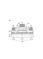
- FIG. 1 is a schematic cross-sectional view showing the configuration of a transistor according to an embodiment of the present invention.
- FIG. 1 is a schematic cross-sectional view showing the configuration of a transistor according to an embodiment of the present invention.
- FIG. 1 is a schematic cross-sectional view showing the configuration of a transistor according to an embodiment of the present invention.
- FIG. 1 is a schematic cross-sectional view showing the configuration of a transistor according to an embodiment of the present invention.
- FIG. 1 is a schematic cross-sectional view showing the configuration of a transistor according to an embodiment of the present invention.
- ⁇ includes A, B or C
- ⁇ includes any one of A, B and C
- ⁇ includes one selected from the group consisting of A, B and C
- ⁇ includes multiple combinations of A to C, unless otherwise specified.
- these expressions do not exclude cases where ⁇ includes other elements.
- the words “above” or “above” or “bottom” or “lower” are used in explanations, but as a general rule, the substrate on which the structure is formed is used as a reference, and the structure is The direction toward an object is defined as ⁇ upward'' or ⁇ upward.'' Conversely, the direction from the structure toward the substrate is defined as “downward” or “downward.” Therefore, when referring to a structure on a substrate, the surface of the structure facing the substrate is the bottom surface of the structure, and the surface opposite thereto is the top surface of the structure. Further, the expression “structure on a substrate” merely describes the vertical relationship between the substrate and the structure, and other members may be arranged between the substrate and the structure. Furthermore, the words “above” or “above” or “below” or “lower” mean the order of lamination in a structure in which multiple layers are laminated, even if they do not overlap in a plan view. good.
- FIG. 1 is a schematic cross-sectional view showing the configuration of a transistor 10 according to an embodiment of the present invention.
- the transistor 10 includes an amorphous substrate 100, a base layer 110, a first buffer layer 120, a first nitride semiconductor layer 140, a second nitride semiconductor layer 150, and a gate insulating layer 160. , a gate electrode layer 170, a source electrode layer 180, and a drain electrode layer 190.
- Base layer 110 is provided on amorphous substrate 100.
- the first buffer layer 120 is provided on the base layer 110.
- the first nitride semiconductor layer 140 has an island-like pattern and is provided on the first buffer layer 120.
- the second nitride semiconductor layer 150 covers the first nitride semiconductor layer 140 and is provided on the first nitride semiconductor layer 140 .
- the gate insulating layer 160 overlaps with the first nitride semiconductor layer 140 and is provided on the second nitride semiconductor layer 150.
- the gate electrode layer 170 overlaps with the first nitride semiconductor layer 140 and is provided on the gate insulating layer 160.
- Each of the source electrode layer 180 and the drain electrode layer 190 is provided on the second nitride semiconductor layer 150 exposed from the gate insulating layer 160. Further, each of the source electrode layer 180 and the drain electrode layer 190 is in contact with the second nitride semiconductor layer 150.
- the first nitride semiconductor layer 140 can be patterned using photolithography.
- the first nitride semiconductor layer 140 is located between the source electrode layer 180 and the drain electrode layer 190 and does not overlap with the source electrode layer 180 and the drain electrode layer 190.
- the first nitride semiconductor layer 140 is in contact with the second nitride semiconductor layer 150. Further, the first nitride semiconductor contained in the first nitride semiconductor layer 140 is different from the second nitride semiconductor contained in the second nitride semiconductor layer 150. Therefore, a heterojunction with band discontinuity is formed at the interface between the first nitride semiconductor layer 140 and the second nitride semiconductor layer 150, and due to natural polarization and piezo effect, a high concentration and A high mobility two-dimensional electron gas (2DEG) 145 is generated.
- the first nitride semiconductor layer 140 and the second nitride semiconductor layer 150 can function as a channel layer and a polarization layer, respectively. That is, the transistor 10 is a so-called HEMT.
- the transistor 10 may have a configuration in which the base layer 110 or the gate insulating layer 160 is not provided.
- the gate electrode layer 170 is in contact with the second nitride semiconductor layer 150 and functions as a so-called Schottky gate electrode.
- the amorphous substrate 100 is a support substrate for the transistor 10. Although details will be described later, since the first nitride semiconductor layer 140 and the second nitride semiconductor layer 150 are formed by sputtering, the amorphous substrate 100 has a heat resistance of, for example, about 600°C. All you have to do is stay there. Therefore, for example, an amorphous glass substrate can be used as the amorphous substrate 100. Further, as the amorphous substrate 100, a resin substrate such as a polyimide substrate, an acrylic substrate, a siloxane substrate, or a fluororesin substrate can also be used. Such an amorphous glass substrate or a resin substrate is a substrate that can be made to have a large area.
- the base layer 110 can prevent impurities from the amorphous substrate 100 or impurities from the outside (eg, moisture, sodium (Na), etc.) from diffusing.
- a silicon nitride (SiN x ) film or the like can be used as the base layer 110.
- a laminated film of a silicon oxide (SiO x ) film and a silicon nitride (SiN x ) film can also be used as the base layer 110.
- the first buffer layer 120 can control the crystal orientation of the first nitride semiconductor layer 140 formed by sputtering and improve the crystallinity of the first nitride semiconductor layer 140. Specifically, the first buffer layer 120 can control the crystallinity of the first nitride semiconductor layer 140 so that the first nitride semiconductor layer 140 has c-axis orientation. For example, when the first nitride semiconductor is gallium nitride, gallium nitride having a hexagonal close-packed structure grows in the c-axis direction to minimize surface energy. By forming a film, crystal growth of gallium nitride in the c-axis direction is promoted.
- the first buffer layer 120 a material having a hexagonal close-packed structure, a face-centered cubic structure, or a structure similar thereto can be used.
- a structure similar to a hexagonal close-packed structure or a face-centered cubic structure includes a crystal structure in which the c-axis is not at 90° with respect to the a-axis and the b-axis.
- the first buffer layer 120 using a material having a hexagonal close-packed structure or a similar structure is oriented in the (0001) direction, that is, the c-axis direction (hereinafter referred to as hexagonal close-packed structure), with respect to the amorphous substrate 100. (referred to as the (0001) orientation of a dense structure).
- the first buffer layer 120 using a material having a face-centered cubic structure or a structure similar thereto is oriented in the (111) direction with respect to the amorphous substrate 100 (hereinafter referred to as ( 111) Orientation). Since the first buffer layer 120 has a (0001) orientation of a hexagonal close-packed structure or a (111) orientation of a face-centered cubic structure, the c-axis direction of gallium nitride deposited on the first buffer layer 120 As a result, the first nitride semiconductor layer 140 has a c-axis orientation with high crystallinity.
- the crystallinity of the first nitride semiconductor layer 140 on the first buffer layer 120 is affected by the surface condition of the first buffer layer 120. Therefore, the first buffer layer 120 preferably has a smooth surface with small irregularities.
- the arithmetic mean roughness (Ra) of the surface of the first buffer layer 120 is preferably smaller than 2.3 nm.
- the root mean square roughness (Rq) of the surface of the first buffer layer 120 is preferably smaller than 2.9 nm.
- the first nitride semiconductor layer 140 has a c-axis orientation with higher crystallinity.
- the thickness of the first buffer layer 120 is preferably 50 nm or more.
- the first buffer layer 120 a conductive material or an insulating material may be used.
- the first buffer layer 120 can be formed using any method (apparatus) such as sputtering or CVD.
- the conductive materials of the first buffer layer 120 include titanium (Ti), magnesium (Mg), aluminum (Al), silver (Ag), calcium (Ca), nickel (Ni), copper (Cu), and strontium (Sr). ), rhodium (Rh), palladium (Pd), cerium (Ce), ytterbium (Yb), iridium (Ir), platinum (Pt), gold (Au), lead (Pb), actinium (Ac), or thorium ( Th) or an alloy thereof can be used.
- titanium nitride (TiN x ), titanium oxide (TiO x ), graphene, zinc oxide (ZnO), magnesium diboride (MgB 2 ), BiLaTiO, SrFeO, BiFeO , BaFeO, ZnFeO, PMnN-PZT, or the like can be used as the conductive material of the first buffer layer 120.
- titanium nitride (TiN x ), titanium oxide (TiO x ), graphene, zinc oxide (ZnO), magnesium diboride (MgB 2 ), BiLaTiO, SrFeO, BiFeO , BaFeO, ZnFeO, PMnN-PZT, or the like can be used as the first buffer layer 120.
- silicon (Si), germanium (Ge), or an alloy thereof can be used as the conductive material for the first buffer layer 120.
- silicon and germanium are semiconductor materials, they have higher conductivity than the insulating materials described below. Therefore, in this specification, semiconductor materials such as silicon and germanium are included in conductive materials.
- Insulating materials for the first buffer layer 120 include aluminum nitride (AlN), aluminum oxide (Al 2 O 3 ), silicon carbide (SiC), lithium niobate (LiNbO), BiLaTiO, SrFeO, SrFeO, BiFeO, BaFeO, ZnFeO, PMnN-PZT, biological apatite (BAp), or the like can be used.
- AlN aluminum nitride
- Al 2 O 3 silicon carbide
- SiC silicon carbide
- LiNbO lithium niobate
- BiLaTiO SrFeO, SrFeO, BiFeO, BaFeO, ZnFeO, PMnN-PZT, biological apatite (BAp), or the like
- BAp biological apatite
- the first nitride semiconductor layer 140 and the second nitride semiconductor layer 150 can function as a channel layer and a polarization layer of the HEMT, respectively.
- the first nitride semiconductor layer 140 and the second nitride semiconductor layer 150 can be made of gallium nitride (GaN) and aluminum gallium nitride (AlGaN) compound semiconductors, respectively, but are not limited thereto.
- each of the first nitride semiconductor layer 140 and the second nitride semiconductor layer 150 may be made of indium nitride (InN), aluminum indium nitride (AlInN), indium gallium nitride (InGaN), or aluminum indium gallium nitride (AlInGaN). ) can also be used.
- InN indium nitride
- AlInN aluminum indium nitride
- InGaN indium gallium nitride
- AlInGaN aluminum indium gallium nitride
- the first nitride semiconductor layer 140 Since the first nitride semiconductor layer 140 is formed on the first buffer layer 120, the first nitride semiconductor layer 140 has a c-axis orientation with high crystallinity. Further, since the second nitride semiconductor layer 150 is formed on the first nitride semiconductor layer 140 having a highly crystalline c-axis orientation, the second nitride semiconductor layer 150 also has a highly crystalline c-axis orientation. It has a high c-axis orientation.
- An amorphous substrate 100 is placed in a vacuum chamber, facing a gallium nitride target.
- the composition ratio of gallium nitride in the gallium nitride target is preferably 0.7 or more and 2 or less of gallium to nitrogen.
- nitrogen can be supplied to the vacuum chamber.
- the composition ratio of gallium nitride in the gallium nitride target preferably includes more gallium than nitrogen.
- nitrogen can be supplied using a nitrogen radical source.
- the sputtering power source may be a DC power source, an RF power source, or a pulsed DC power source.
- the amorphous substrate 100 within the vacuum chamber may be heated.
- the amorphous substrate 100 can be heated at room temperature or higher and lower than 600°C, preferably at 100°C or higher and lower than 400°C. At this temperature, it can be applied even to amorphous glass substrates with low heat resistance. Moreover, this temperature is lower than the deposition temperature in MOCVD or HVPE.
- gallium nitride can be formed by using an aluminum gallium nitride target instead of a gallium nitride target.
- silicon oxide (SiO x ), aluminum oxide (AlO x ), hafnium oxide (HfO x ), lanthanum oxide (LaO x ), silicon nitride (SiN x ), aluminum nitride (AlN x ), or the like is used. Can be used.
- the gate insulating layer 160 may be a single film or a laminated film.
- the gate electrode layer 170 metals such as aluminum (Al), titanium (Ti), platinum (Pt), nickel (Ni), tantalum (Ta), or gold (Au), or alloys thereof can be used.
- the gate electrode layer 170 may be a single film or a laminated film.
- Each of the source electrode layer 180 and the drain electrode layer 190 is made of metal such as aluminum (Al), titanium (Ti), platinum (Pt), nickel (Ni), tantalum (Ta), or gold (Au), or a metal such as these. Alloys can be used.
- Each of the source electrode layer 180 and the drain electrode layer 190 may be a single film or a laminated film.
- the first nitride semiconductor layer 140 has an island-like pattern and does not overlap with the source electrode layer 180 and the drain electrode layer 190. Therefore, the 2DEG 145 generated by the heterojunction also does not overlap with the source electrode layer 180 and the drain electrode layer 190. Therefore, leakage current between the 2DEG 145 formed in the first nitride semiconductor layer 140 and the source electrode layer 180 or the drain electrode layer 190 can be suppressed, so that the transistor 10 is of normally-off type (enhancement type). ). Furthermore, by patterning the first nitride semiconductor layer 140, the first nitride semiconductor layer 140 can be formed at any position, so the transistor 10 has a structure with a high degree of freedom in design.
- FIG. 2 is a schematic cross-sectional view showing the configuration of a transistor 10A according to an embodiment of the present invention. Note that in the following description, when the configuration of the transistor 10A is similar to the configuration of the transistor 10, the description of the configuration of the transistor 10A may be omitted.
- the transistor 10A includes an amorphous substrate 100, a base layer 110, a first buffer layer 120A, a first nitride semiconductor layer 140, a second nitride semiconductor layer 150, and a gate insulating layer 160. , a gate electrode layer 170, a source electrode layer 180, and a drain electrode layer 190.
- the first buffer layer 120A is patterned so that the base layer 110 is exposed. Further, the exposed base layer 110 is covered with a second nitride semiconductor layer 150. That is, the first buffer layer 120A includes a first region 121A-1 that overlaps with the first nitride semiconductor layer 140 and a second region 121A-2 that does not overlap with the first nitride semiconductor layer 140.
- the ends of each of the first region 121A-1 and the second region 121A-2 are covered with a second nitride semiconductor layer 150. Further, the first region 121A-1 and the second region 121A-2 are separated from each other via the second nitride semiconductor layer 150, and are electrically connected via the second nitride semiconductor layer 150. is insulated.
- the first buffer layer 120A can be patterned using photolithography.
- the first region 121A-1 and the first nitride semiconductor layer 140 are located between the source electrode layer 180 and the drain electrode layer 190 and do not overlap with the source electrode layer 180 and the drain electrode layer 190.
- the second region 121A-2 can be used as a routing wiring.
- the transistor 10A may have a configuration in which the second region 121A-2 is not provided.
- the transistor 10A according to Modification Example 1 not only the first nitride semiconductor layer 140 but also the first region 121A-1 under the first nitride semiconductor layer 140 are connected to the source electrode layer 180 and the drain electrode layer. It does not overlap with 190. Further, the first region 121A-1 and the second region 121A-2 are electrically insulated. Therefore, even if the first buffer layer 120A includes a conductive material, the first buffer layer 120A (more specifically, the first region 121A-1) and the source electrode layer 180 or the drain electrode layer Since leakage current between the transistor 10A and the transistor 190 can be suppressed, the transistor 10A has normally-off type (enhancement type) characteristics. Further, by patterning the first buffer layer 120A, the transistor 10A has normally-off type (enhancement type) properties without depending on the material of the first buffer layer 120A. , has a structure with a high degree of design freedom.
- FIG. 3 is a schematic cross-sectional view showing the configuration of a transistor 10B according to an embodiment of the present invention. Note that in the following description, when the configuration of the transistor 10B is similar to the configuration of the transistor 10 or the transistor 10A, the description of the configuration of the transistor 10B may be omitted.
- the transistor 10B includes an amorphous substrate 100, a base layer 110, a first buffer layer 120A, a second buffer layer 130B, a first nitride semiconductor layer 140, and a second nitride semiconductor layer. layer 150, a gate insulating layer 160, a gate electrode layer 170, a source electrode layer 180, and a drain electrode layer 190.
- the second buffer layer 130B is provided between the first buffer layer 120A and the first nitride semiconductor layer 140.
- the second buffer layer 130B is patterned to cover the first region 121A-1 and expose the second region 121A-2. Furthermore, the exposed second region 121A-2 is covered with the second nitride semiconductor layer 150. That is, the ends of each of the first region 121A-1 and the second region 121A-2 are covered with the second buffer layer 130B.
- the second buffer layer 130B has the same function as the first buffer layer 120A. That is, the second buffer layer 130B can also control the crystal orientation of the first nitride semiconductor layer 140 formed by sputtering and improve the crystallinity of the first nitride semiconductor layer 140. However, an insulating material is used as the second buffer layer 130B. Since the second buffer layer 130B includes an insulating material, the first region 121A-1 and the second region 121A-2 are separated via the second buffer layer 130B, and It is electrically insulated via the buffer layer 130B.
- the second buffer layer 130B can be patterned using photolithography.
- the second buffer layer 130B may or may not overlap the source electrode layer 180 or the drain electrode layer 190.
- the transistor 10B may have a structure in which the second buffer layer 130B is not patterned.
- the second buffer layer 130B includes an insulating material, and the first region 121A-1 and the second region 121A-2 are connected to each other through the second buffer layer 130B. It is insulated. Therefore, even if the first buffer layer 120A includes a conductive material, the first buffer layer 120A (more specifically, the first region 121A-1) and the source electrode layer 180 or the drain electrode layer Since leakage current between the transistor 10B and the transistor 190 can be suppressed, the transistor 10B has normally-off type (enhancement type) characteristics.
- the transistor 10B can be a normally-off type (enhancement transistor) without depending on the material of the first buffer layer 120A.
- the transistor 10B has a structure with a high degree of freedom in design.
- FIG. 4 is a schematic cross-sectional view showing the configuration of a transistor 20 according to an embodiment of the present invention.
- the configuration of the transistor 20 is similar to the configuration of the transistor 10, the description of the configuration of the transistor 20 may be omitted.
- the transistor 20 includes an amorphous substrate 200, a base layer 210, a source electrode layer 280, a drain electrode layer 290, a first buffer layer 220, a first nitride semiconductor layer 240, a second A nitride semiconductor layer 250, a gate insulating layer 260, and a gate electrode layer 270 are included.
- Base layer 210 is provided on amorphous substrate 200.
- the source electrode layer 280 and the drain electrode layer 290 are provided on the base layer 210.
- the first buffer layer 220 is located between the source electrode layer 280 and the drain electrode layer 290 and is provided on the base layer 210.
- the first nitride semiconductor layer 240 has an island-like pattern and is provided on the first buffer layer 120.
- the second nitride semiconductor layer 250 covers the source electrode layer 280, the drain electrode layer 290, and the first nitride semiconductor layer 240, and covers the source electrode layer 280, the drain electrode layer 290, and the first nitride semiconductor layer. 240.
- Each of the source electrode layer 280 and the drain electrode layer 290 is in contact with the second nitride semiconductor layer 250.
- the end portion of the first buffer layer 220 is covered with a second nitride semiconductor layer 250.
- the gate insulating layer 260 overlaps with the first nitride semiconductor layer 240 and is provided on the second nitride semiconductor layer 250.
- the gate electrode layer 270 overlaps with the first nitride semiconductor layer 240 and is provided on the gate insulating layer 260.
- the transistor 20 is a so-called HEMT. That is, the first nitride semiconductor layer 240 and the second nitride semiconductor layer 250 function as a channel layer and a polarization layer, respectively, and the first nitride semiconductor layer 240 and the second nitride semiconductor layer 250 A two-dimensional electron gas (2DEG) 245 with high concentration and high mobility is generated near the junction interface.
- 2DEG two-dimensional electron gas
- the first buffer layer 220 has the same function as the first buffer layer 120 described above. However, a conductive material is used as the first buffer layer 220.
- the first buffer layer 220 is provided in the same layer as the source electrode layer 280 and the drain electrode layer 290. That is, the first buffer layer 220, the source electrode layer 280, and the drain electrode layer 290 are formed by patterning the same conductive material.
- the first buffer layer 220, the source electrode layer 280, and the drain electrode layer 290 can be patterned using photolithography.
- the source electrode layer 280 and the drain electrode layer 290 are formed by patterning the conductive material of the first buffer layer 220, so the first buffer layer 220 is formed by forming the source electrode layer 280 and the drain electrode layer It does not overlap with 290.
- the first buffer layer 220 and the first nitride semiconductor layer 240 do not overlap the source electrode layer 280 and the drain electrode layer 290. Further, the first buffer layer 220 is electrically insulated from the source electrode layer 280 and the drain electrode layer 290 via the second nitride semiconductor layer 250. Therefore, leakage current between the first buffer layer 220 and the source electrode layer 280 or the drain electrode layer 290 can be suppressed, so the transistor 20 has normally-off (enhancement) characteristics. Further, since the source electrode layer 280 and the drain electrode layer 290 can be formed in the same process as the first buffer layer 220, the manufacturing takt time of the transistor 20 can be shortened and the manufacturing cost can be reduced.
- the first buffer layer 220 does not overlap with the source electrode layer 280 and the drain electrode layer 290. Therefore, the first nitride semiconductor layer 240 can be formed according to the pattern of the first buffer layer 220, so the transistor 20 has a structure with a high degree of freedom in design.
- FIG. 5 is a schematic cross-sectional view showing the configuration of a transistor 20A according to an embodiment of the present invention. Note that in the following description, when the configuration of the transistor 20A is similar to the configuration of the transistor 20, the description of the configuration of the transistor 20 may be omitted.
- the transistor 20A includes an amorphous substrate 200, a base layer 210, a source electrode layer 280, a drain electrode layer 290, a first buffer layer 220, a second buffer layer 230A, and a first nitride layer.
- a semiconductor layer 240, a second nitride semiconductor layer 250, a gate insulating layer 260, and a gate electrode layer 270 are included.
- the second buffer layer 230A is provided between the first buffer layer 220 and the first nitride semiconductor layer 240.
- the second buffer layer 230A is provided between the first buffer layer 220 and the first nitride semiconductor layer 240.
- the second buffer layer 230A covers the first buffer layer 220 and is patterned so that the source electrode layer 280 and the drain electrode layer 290 are exposed. Further, the exposed source electrode layer 280 and drain electrode layer 290 are covered with the second nitride semiconductor layer 250. That is, the ends of each of the first buffer layer 220, source electrode layer 280, and drain electrode layer 290 are covered with the second buffer layer 230A.
- the second buffer layer 230A has the same function as the first buffer layer 220A. However, an insulating material is used as the second buffer layer 230A. Since the second buffer layer 230A contains an insulating material, the first buffer layer 220 and the source electrode layer 280 or the drain electrode layer 290 are separated via the second buffer layer 230A, and It is further electrically insulated via the buffer layer 230A.
- the second buffer layer 230A can be patterned using photolithography.
- the second buffer layer 230A may or may not overlap the source electrode layer 280 or the drain electrode layer 290. Note that the transistor 20A may have a structure in which the second buffer layer 230A is not patterned.
- the second buffer layer 230A includes an insulating material, and the first buffer layer 220 is connected to the source electrode layer 280 and the drain electrode layer 290 via the second buffer layer 230A. Electrically insulated. Therefore, leakage current between the first buffer layer 220 and the source electrode layer 280 or the drain electrode layer 290 can be suppressed, so the transistor 20 has normally-off (enhancement) characteristics. Further, since the source electrode layer 280 and the drain electrode layer 290 can be formed in the same process as the first buffer layer 220, the manufacturing takt time of the transistor 20 can be shortened and the manufacturing cost can be reduced. Furthermore, by patterning the second buffer layer 230A to cover the first buffer layer 220, the transistor 20A can be a normally-off type ( Since the transistor 20A has enhancement type characteristics, the transistor 20A has a structure with a high degree of freedom in design.
- the embodiments described above as embodiments of the present invention can be implemented in appropriate combinations as long as they do not contradict each other.
- the gist of the present invention may also include additions, deletions, or design changes of constituent elements, or additions, omissions, or condition changes of steps, based on each embodiment, by a person skilled in the art. It is within the scope of the present invention as long as it has the following.
- 10, 10A, 10B, 20, 20A transistor, 100, 200: amorphous substrate, 110, 210: base layer, 120, 120A, 220, 220A: first buffer layer, 121A-1: first area, 121A-2: second area, 130B, 230A: second buffer layer, 140, 240: first nitride semiconductor layer, 145, 245: Two-dimensional electron gas (2DEG), 150, 250: second nitride semiconductor layer, 160, 260: gate insulating layer, 170, 270: gate electrode layer, 180, 280: source electrode layer, 190, 290: drain electrode layer,
- 2DEG Two-dimensional electron gas
Landscapes
- Junction Field-Effect Transistors (AREA)
- Thin Film Transistor (AREA)
Abstract
トランジスタは、非晶質基板と、非晶質基板の上の第1のバッファー層と、第1のバッファー層の上において、島状に設けられた第1の窒化物半導体層と、第1の窒化物半導体層の上において、第1の窒化物半導体層を覆う第2の窒化物半導体層と、第2の窒化物半導体層の上において、第1の窒化物半導体層と重畳するゲート電極層と、を含む。
Description
本発明の一実施形態は、化合物半導体を利用したトランジスタ、特に高電子移動度トランジスタ(High Electron Mobility Transistor:HEMT)に関する。
窒化ガリウム(GaN)は、バンドギャップの大きい直接遷移半導体である。窒化ガリウムの性質に着目すると、窒化ガリウムは、飽和電子移動度が大きく、耐圧が高いという特徴を有する。近年では、この窒化ガリウムの特徴を利用し、高周波パワーデバイス用途のトランジスタ、いわゆるHEMTの開発が進められている。
HEMTでは、窒化ガリウムだけでなく、窒化ガリウムに接して窒化アルミニウムガリウム(AlGaN)を設けたヘテロ接合構造体を有する。窒化ガリウムと窒化アルミニウムガリウムとの界面では、半導体層として機能する窒化ガリウムの自発分極および分極層として機能する窒化アルミニウムガリウムのピエゾ効果によって電荷が誘起され、高密度の二次元電子ガス(2DEG)が形成される。HEMTの二次元電子ガスの濃度は大きく、また、飽和電子移動度も高いことから、HEMTでは高速動作が可能となる。
HEMTの窒化ガリウムは、一般的に、大面積化が困難なサファイア基板上に、MOCVD(Metal Organic Chemical Vapor Deposition)またはHVPE(Hydride Vapor Phase Epitaxy)を用いて800℃~1000℃という高温で成膜される。
上述したように、一般的には、窒化ガリウムはサファイア基板上に高温で成膜されるが、サファイア基板は大面積化が困難であり、製造コストを削減することが難しい。そのため、ガラス基板のような大面積化が可能な非晶質基板上に窒化ガリウムのc軸配向性を制御するバッファー層(配向層)を設け、スパッタリングによって窒化ガリウムを低温で成膜する技術開発も進められている。しかしながら、一般的に、HEMTは、ノーマリーオン型(デプレッション型)の性質を有しやすい問題があった。
本発明の一実施形態は、上記問題に鑑み、ノーマリーオンを抑制し、設計自由度の高い構造を有するトランジスタを提供することを目的の一つとする。
本発明の一実施形態に係るトランジスタは、非晶質基板と、非晶質基板の上の第1のバッファー層と、第1のバッファー層の上において、島状に設けられた第1の窒化物半導体層と、第1の窒化物半導体層の上において、第1の窒化物半導体層を覆う第2の窒化物半導体層と、第2の窒化物半導体層の上において、第1の窒化物半導体層と重畳するゲート電極層と、を含む。
以下、本発明に係る各実施形態について、図面を参照しつつ説明する。なお、各実施形態はあくまで一例にすぎず、当業者が、発明の主旨を保ちつつ適宜変更することによって容易に想到し得るものについても、当然に本発明の範囲に含まれる。また、図面は、説明をより明確にするため、実際の態様に比べ、各部の幅、厚さ、または形状などが模式的に表される場合がある。しかし、図示された形状などはあくまで一例であって、本発明の解釈を限定するものではない。
本明細書において「αはA、BまたはCを含む」、「αはA、BおよびCのいずれかを含む」、「αはA、BおよびCからなる群から選択される一つを含む」、といった表現は、特に明示が無い限り、αがA~Cの複数の組み合わせを含む場合を排除しない。さらに、これらの表現は、αが他の要素を含む場合も排除しない。
本明細書において、説明の便宜上、「上」もしくは「上方」または「下」もしくは「下方」という語句を用いて説明するが、原則として、構造物が形成される基板を基準とし、基板から構造物に向かう方向を「上」または「上方」とする。逆に、構造物から基板に向かう方向を「下」または「下方」とする。したがって、基板上の構造物という表現において、基板と向き合う方向の構造物の面が構造物の下面となり、その反対側の面が構造物の上面となる。また、基板上の構造物という表現においては、基板と構造物との上下関係を説明しているに過ぎず、基板と構造物との間に他の部材が配置されていてもよい。さらに、「上」もしくは「上方」または「下」もしくは「下方」の語句は、複数の層が積層された構造における積層順を意味するものであり、平面視において重畳する位置関係になくてもよい。
本明細書において、各構成に付記される「第1」、「第2」、または「第3」などの文字は、各構成を区別するために用いられる便宜的な標識であり、特段の説明がない限り、それ以上の意味を有さない。
本明細書および図面において、同一または類似する複数の構成を総じて表記する際には同一の符号を用い、これらの複数の構成のそれぞれを区別して表記する際には、小文字または大文字のアルファベットを添えて表記する場合がある。また、1つの構成のうちの複数の部分を区別して表記する際には、ハイフンと自然数を用いる場合がある。
以下の各実施形態は、技術的な矛盾を生じない限り、互いに組み合わせることができる。
<第1実施形態>
図1は、本発明の一実施形態に係るトランジスタ10の構成を示す模式的な断面図である。
図1は、本発明の一実施形態に係るトランジスタ10の構成を示す模式的な断面図である。
図1に示すように、トランジスタ10は、非晶質基板100、下地層110、第1のバッファー層120、第1の窒化物半導体層140、第2の窒化物半導体層150、ゲート絶縁層160、ゲート電極層170、ソース電極層180、およびドレイン電極層190を含む。下地層110は、非晶質基板100上に設けられている。第1のバッファー層120は、下地層110上に設けられている。第1の窒化物半導体層140は、島状のパターンを有し、第1のバッファー層120上に設けられている。第2の窒化物半導体層150は、第1の窒化物半導体層140を覆い、第1の窒化物半導体層140上に設けられている。ゲート絶縁層160は、第1の窒化物半導体層140と重畳し、第2の窒化物半導体層150上に設けられている。ゲート電極層170は、第1の窒化物半導体層140と重畳し、ゲート絶縁層160上に設けられている。ソース電極層180およびドレイン電極層190の各々は、ゲート絶縁層160から露出された第2の窒化物半導体層150上に設けられている。また、ソース電極層180およびドレイン電極層190の各々は、第2の窒化物半導体層150と接している。
第1の窒化物半導体層140は、フォトリソグラフィーを用いて、パターニングすることができる。第1の窒化物半導体層140は、ソース電極層180とドレイン電極層190との間に位置し、ソース電極層180およびドレイン電極層190と重畳していない。
第1の窒化物半導体層140は、第2の窒化物半導体層150と接している。また、第1の窒化物半導体層140に含まれる第1の窒化物半導体は、第2の窒化物半導体層150に含まれる第2の窒化物半導体と異なる。そのため、第1の窒化物半導体層140と第2の窒化物半導体層150との界面には、バンド不連続を有するヘテロ接合が形成され、自然分極とピエゾ効果により、接合界面近傍に高濃度および高移動度の2次元電子ガス(2DEG)145が生成される。換言すると、第1の窒化物半導体層140および第2の窒化物半導体層150は、それぞれ、チャネル層および分極層として機能することができる。すなわち、トランジスタ10は、いわゆるHEMTである。
なお、トランジスタ10は、下地層110またはゲート絶縁層160が設けられない構成を有していてもよい。ゲート絶縁層160が設けられない場合、ゲート電極層170は、第2の窒化物半導体層150と接し、いわゆるショットキーゲート電極として機能する。
非晶質基板100は、トランジスタ10の支持基板である。詳細は後述するが、第1の窒化物半導体層140および第2の窒化物半導体層150はスパッタリングによって成膜されるため、非晶質基板100は、例えば、600℃程度の耐熱性を有していればよい。そのため、例えば、非晶質基板100として、非晶質ガラス基板を用いることができる。また、非晶質基板100として、ポリイミド基板、アクリル基板、シロキサン基板、またはフッ素樹脂基板などの樹脂基板も用いることができる。このような非晶質ガラス基板または樹脂基板は、大面積化が可能な基板である。
下地層110は、非晶質基板100からの不純物または外部からの不純物(例えば、水分またはナトリウム(Na)など)の拡散を防止することができる。例えば、下地層110として、窒化シリコン(SiNx)膜などを用いることができる。また、下地層110として、酸化シリコン(SiOx)膜と窒化シリコン(SiNx)膜との積層膜を用いることもできる。
第1のバッファー層120は、スパッタリングによって成膜される第1の窒化物半導体層140の結晶配向性を制御し、第1の窒化物半導体層140の結晶性を向上させることができる。具体的には、第1のバッファー層120は、第1の窒化物半導体層140がc軸配向性を有するように、第1の窒化物半導体層140の結晶性を制御することができる。例えば、第1の窒化物半導体が窒化ガリウムである場合、六方最密構造を有する窒化ガリウムは表面エネルギーを最小化するようにc軸方向に成長するが、第1のバッファー層120上に窒化ガリウムを成膜することにより、窒化ガリウムのc軸方向への結晶成長が促進される。第1のバッファー層120として、六方最密構造、面心立方構造、またはそれらに準ずる構造を有する材料を用いることができる。ここで、六方最密構造または面心立方構造に準ずる構造とは、a軸およびb軸に対してc軸が90°とならない結晶構造を含むものである。六方最密構造またはそれに準ずる構造を有する材料を用いた第1のバッファー層120は、非晶質基板100に対して(0001)方向、すなわち、c軸方向に配向している(以下、六方最密構造の(0001)配向という。)。また、面心立方構造またはそれに準ずる構造を有する材料を用いた第1のバッファー層120は、非晶質基板100に対して(111)方向に配向している(以下、面心立方構造の(111)配向という。)。第1のバッファー層120が六方最密構造の(0001)配向または面心立方構造の(111)配向を有することにより、第1のバッファー層120上に成膜される窒化ガリウムのc軸方向への結晶成長が促進され、その結果、第1の窒化物半導体層140は結晶性の高いc軸配向を有する。
第1のバッファー層120上の第1の窒化物半導体層140の結晶性は、第1のバッファー層120の表面状態の影響を受ける。そのため、第1のバッファー層120は、凹凸が小さく、平滑な表面を有することが好ましい。例えば、第1のバッファー層120の表面の算術平均粗さ(Ra)は、2.3nmよりも小さいことが好ましい。また、第1のバッファー層120の表面の二乗平均平方根粗さ(Rq)は、2.9nmよりも小さいことが好ましい。第1のバッファー層120の表面粗さが上記条件である場合、第1の窒化物半導体層140は、より結晶性の高いc軸配向を有する。なお、第1のバッファー層120の膜厚は、50nm以上であることが好ましい。
第1のバッファー層120として、導電性材料が用いられてもよく、絶縁性材料が用いられてもよい。第1のバッファー層120は、スパッタリングまたはCVDなどの任意の方法(装置)を用いて成膜することができる。
第1のバッファー層120の導電性材料として、チタン(Ti)、マグネシウム(Mg)、アルミニウム(Al)、銀(Ag)、カルシウム(Ca)、ニッケル(Ni)、銅(Cu)、ストロンチウム(Sr)、ロジウム(Rh)、パラジウム(Pd)、セリウム(Ce)、イッテルビウム(Yb)、イリジウム(Ir)、白金(Pt)、金(Au)、鉛(Pb)、アクチニウム(Ac)、もしくはトリウム(Th)、またはこれらの合金を用いることができる。また、第1のバッファー層120の導電性材料として、窒化チタン(TiNx)、酸化チタン(TiOx)、グラフェン、酸化亜鉛(ZnO)、二ホウ化マグネシウム(MgB2)、BiLaTiO、SrFeO、BiFeO、BaFeO、ZnFeO、またはPMnN-PZTなどを用いることができる。特に、第1のバッファー層120として、チタン、グラフェン、または酸化亜鉛を用いることが好ましい。
また、第1のバッファー層120の導電性材料として、シリコン(Si)もしくはゲルマニウム(Ge)またはこれらの合金などを用いることができる。シリコンおよびゲルマニウムは、半導体材料であるが、後述する絶縁性材料よりは高い導電性を有する。そのため、本明細書では、シリコンおよびゲルマニウムなどの半導体材料は、導電性材料に含まれるものとする。
第1のバッファー層120の絶縁性材料として、窒化アルミニウム(AlN)、酸化アルミニウム(Al2O3)、炭化シリコン(SiC)、ニオブ酸リチウム(LiNbO)、BiLaTiO、SrFeO、SrFeO、BiFeO、BaFeO、ZnFeO、PMnN-PZT、または生体アパタイト(BAp)などを用いることができる。特に、第1のバッファー層120として、窒化アルミニウムまたは炭化シリコンを用いることが好ましい。
第1の窒化物半導体層140および第2の窒化物半導体層150は、上述したように、それぞれ、HEMTのチャネル層および分極層として機能することができる。第1の窒化物半導体層140および第2の窒化物半導体層150は、それぞれ、窒化ガリウム(GaN)および窒化アルミニウムガリウム(AlGaN)化合物半導体を用いることができるが、これに限られない。例えば、第1の窒化物半導体層140および第2の窒化物半導体層150の各々として、窒化インジウム(InN)、窒化アルミニウムインジウム(AlInN)、窒化インジウムガリウム(InGaN)、または窒化アルミニウムインジウムガリウム(AlInGaN)を用いることもできる。
第1の窒化物半導体層140は、第1のバッファー層120上に形成されているため、第1の窒化物半導体層140は、結晶性の高いc軸配向を有する。また、第2の窒化物半導体層150は、結晶性の高いc軸配向を有する第1の窒化物半導体層140上に形成されているため、第2の窒化物半導体層150も、結晶性の高いc軸配向を有する。
ここで、第1の窒化物半導体層140の形成の一例として、スパッタリングを用いた窒化ガリウムの成膜について説明する。
真空チャンバ内に、窒化ガリウムターゲットと対向して非晶質基板100を配置する。窒化ガリウムターゲットにおける窒化ガリウムの組成比は、窒素に対するガリウムが0.7以上2以下であることが好ましい。また、真空チャンバには、スパッタリングガス(アルゴン(Ar)またはクリプトン(Kr)など)とは別に、窒素を供給することができる。その場合、窒化ガリウムターゲットの窒化ガリウムの組成比は、窒素よりもガリウムが多いことが好ましい。例えば、窒素は、窒素ラジカル供給源を用いて供給することができる。スパッタリング電源は、DC電源、RF電源、またはパルスDC電源のいずれであってもよい。
真空チャンバ内の非晶質基板100は、加熱されてもよい。例えば、非晶質基板100は、室温以上600℃未満、好ましくは100℃以上400℃以下で加熱することができる。この温度であれば、耐熱性の低い非晶質ガラス基板に対しても適用することができる。また、この温度は、MOCVDまたはHVPEでの成膜温度よりも低い。
真空チャンバ内を十分排気した後、スパッタリングガスを供給する。また、所定の圧力で非晶質基板100と窒化ガリウムターゲットとの間に電圧を印加してプラズマを生成し、窒化ガリウムを成膜する。
以上、スパッタリングによる窒化ガリウムの成膜方法について説明したが、スパッタリングの構成または条件は適宜変更することができる。なお、窒化ガリウムターゲットではなく、窒化アルミニウムガリウムターゲットを用いれば、窒化アルミニウムガリウムを成膜することができる。
ゲート絶縁層160として、酸化シリコン(SiOx)、酸化アルミニウム(AlOx)、酸化ハフニウム(HfOx)、酸化ランタン(LaOx)、窒化シリコン(SiNx)、または窒化アルミニウム(AlNx)などを用いることができる。ゲート絶縁層160は、単膜であってもよく、積層膜であってもよい。
ゲート電極層170として、アルミニウム(Al)、チタン(Ti)、白金(Pt)、ニッケル(Ni)、タンタル(Ta)、もしくは金(Au)などの金属、またはこれらの合金を用いることができる。ゲート電極層170は、単膜であってもよく、積層膜であってもよい。
ソース電極層180およびドレイン電極層190の各々として、アルミニウム(Al)、チタン(Ti)、白金(Pt)、ニッケル(Ni)、タンタル(Ta)、もしくは金(Au)などの金属、またはこれらの合金を用いることができる。ソース電極層180およびドレイン電極層190の各々は、単膜であってもよく、積層膜であってもよい。
本実施形態に係るトランジスタ10では、第1の窒化物半導体層140が島状のパターンを有し、ソース電極層180およびドレイン電極層190と重畳していない。そのため、ヘテロ接合によって生成された2DEG145も、ソース電極層180およびドレイン電極層190と重畳しない。したがって、第1の窒化物半導体層140に形成される2DEG145とソース電極層180またはドレイン電極層190との間のリーク電流を抑制することができるため、トランジスタ10は、ノーマリーオフ型(エンハンスメント型)の性質を有する。また、第1の窒化物半導体層140がパターニングされることにより、任意の位置に第1の窒化物半導体層140を形成することができるため、トランジスタ10は、設計自由度の高い構造を有する。
<第1実施形態の変形例1>
図2を参照して、トランジスタ10の一変形例について説明する。図2は、本発明の一実施形態に係るトランジスタ10Aの構成を示す模式的な断面図である。なお、以下の説明では、トランジスタ10Aの構成がトランジスタ10の構成と同様であるとき、トランジスタ10Aの構成の説明を省略する場合がある。
図2を参照して、トランジスタ10の一変形例について説明する。図2は、本発明の一実施形態に係るトランジスタ10Aの構成を示す模式的な断面図である。なお、以下の説明では、トランジスタ10Aの構成がトランジスタ10の構成と同様であるとき、トランジスタ10Aの構成の説明を省略する場合がある。
図2に示すように、トランジスタ10Aは、非晶質基板100、下地層110、第1のバッファー層120A、第1の窒化物半導体層140、第2の窒化物半導体層150、ゲート絶縁層160、ゲート電極層170、ソース電極層180、およびドレイン電極層190を含む。第1のバッファー層120Aは、下地層110が露出されるようにパターニングされている。また、露出した下地層110は、第2の窒化物半導体層150によって覆われている。すなわち、第1のバッファー層120Aは、第1の窒化物半導体層140と重畳する第1の領域121A-1、および第1の窒化物半導体層140と重畳しない第2の領域121A-2を含み、第1の領域121A-1および第2の領域121A-2の各々の端部は、第2の窒化物半導体層150によって覆われている。また、第1の領域121A-1と第2の領域121A-2とは、第2の窒化物半導体層150を介して離間されているとともに、第2の窒化物半導体層150を介して電気的に絶縁化されている。
第1のバッファー層120Aは、フォトリソグラフィーを用いて、パターニングすることができる。第1の領域121A-1および第1の窒化物半導体層140は、ソース電極層180とドレイン電極層190との間に位置し、ソース電極層180およびドレイン電極層190と重畳していない。
第1のバッファー層120Aが導電性材料を含む場合、第2の領域121A-2は、引き回し配線として利用することができる。なお、トランジスタ10Aは、第2の領域121A-2が設けられない構成を有していてもよい。
本変形例1に係るトランジスタ10Aでは、第1の窒化物半導体層140だけでなく、第1の窒化物半導体層140の下の第1の領域121A-1も、ソース電極層180およびドレイン電極層190と重畳していない。また、第1の領域121A-1と第2の領域121A-2とは電気的に絶縁化されている。したがって、第1のバッファー層120Aが導電性材料を含む場合であっても、第1のバッファー層120A(より具体的には、第1の領域121A-1)とソース電極層180またはドレイン電極層190との間のリーク電流を抑制することができるため、トランジスタ10Aは、ノーマリーオフ型(エンハンスメント型)の性質を有する。また、第1のバッファー層120Aがパターニングされることにより、トランジスタ10Aは、第1のバッファー層120Aの材料に依存することなく、ノーマリーオフ型(エンハンスメント型)の性質を有するため、トランジスタ10Aは、設計自由度の高い構造を有する。
<第1実施形態の変形例2>
図3を参照して、トランジスタ10の別の変形例について説明する。図3は、本発明の一実施形態に係るトランジスタ10Bの構成を示す模式的な断面図である。なお、以下の説明では、トランジスタ10Bの構成がトランジスタ10またはトランジスタ10Aの構成と同様であるとき、トランジスタ10Bの構成の説明を省略する場合がある。
図3を参照して、トランジスタ10の別の変形例について説明する。図3は、本発明の一実施形態に係るトランジスタ10Bの構成を示す模式的な断面図である。なお、以下の説明では、トランジスタ10Bの構成がトランジスタ10またはトランジスタ10Aの構成と同様であるとき、トランジスタ10Bの構成の説明を省略する場合がある。
図3に示すように、トランジスタ10Bは、非晶質基板100、下地層110、第1のバッファー層120A、第2のバッファー層130B、第1の窒化物半導体層140、第2の窒化物半導体層150、ゲート絶縁層160、ゲート電極層170、ソース電極層180、およびドレイン電極層190を含む。第2のバッファー層130Bは、第1のバッファー層120Aと第1の窒化物半導体層140との間に設けられている。第2のバッファー層130Bは、第1の領域121A-1を覆い、第2の領域121A-2が露出されるようにパターニングされている。また、露出した第2の領域121A-2は、第2の窒化物半導体層150によって覆われている。すなわち、第1の領域121A-1および第2の領域121A-2の各々の端部は、第2のバッファー層130Bによって覆われている。
第2のバッファー層130Bは、第1のバッファー層120Aと同様の機能を有する。すなわち、第2のバッファー層130Bも、スパッタリングによって成膜される第1の窒化物半導体層140の結晶配向性を制御し、第1の窒化物半導体層140の結晶性を向上させることができる。但し、第2のバッファー層130Bとして、絶縁性材料が用いられる。第2のバッファー層130Bが絶縁性材料を含むことにより、第1の領域121A-1と第2の領域121A-2とは、第2のバッファー層130Bを介して離間されるとともに、第2のバッファー層130Bを介して電気的に絶縁化される。
第2のバッファー層130Bは、フォトリソグラフィーを用いて、パターニングすることができる。第2のバッファー層130Bは、ソース電極層180またはドレイン電極層190と重畳していてもよく、重畳していなくてもよい。なお、トランジスタ10Bは、第2のバッファー層130Bがパターニングされていない構成を有していてもよい。
本変形例に係るトランジスタ10Bでは、第2のバッファー層130Bが絶縁性材料を含み、第1の領域121A-1と第2の領域121A-2とが、第2のバッファー層130Bを介して電気的に絶縁化されている。したがって、第1のバッファー層120Aが導電性材料を含む場合であっても、第1のバッファー層120A(より具体的には、第1の領域121A-1)とソース電極層180またはドレイン電極層190との間のリーク電流を抑制することができるため、トランジスタ10Bは、ノーマリーオフ型(エンハンスメント型)の性質を有する。また、第2のバッファー層130Bが第1の領域121A-1を覆うようにパターニングされることにより、トランジスタ10Bは、第1のバッファー層120Aの材料に依存することなく、ノーマリーオフ型(エンハンスメント型)の性質を有するため、トランジスタ10Bは、設計自由度の高い構造を有する。
<第2実施形態>
図4は、本発明の一実施形態に係るトランジスタ20の構成を示す模式的な断面図である。以下の説明では、トランジスタ20の構成がトランジスタ10の構成と同様であるとき、トランジスタ20の構成の説明を省略する場合がある。
図4は、本発明の一実施形態に係るトランジスタ20の構成を示す模式的な断面図である。以下の説明では、トランジスタ20の構成がトランジスタ10の構成と同様であるとき、トランジスタ20の構成の説明を省略する場合がある。
図4に示すように、トランジスタ20は、非晶質基板200、下地層210、ソース電極層280、ドレイン電極層290、第1のバッファー層220、第1の窒化物半導体層240、第2の窒化物半導体層250、ゲート絶縁層260、およびゲート電極層270を含む。下地層210は、非晶質基板200上に設けられている。ソース電極層280およびドレイン電極層290は、下地層210上に設けられている。第1のバッファー層220は、ソース電極層280とドレイン電極層290との間に位置し、下地層210上に設けられている。第1の窒化物半導体層240は、島状のパターンを有し、第1のバッファー層120上に設けられている。第2の窒化物半導体層250は、ソース電極層280、ドレイン電極層290、および第1の窒化物半導体層240を覆い、ソース電極層280、ドレイン電極層290、および第1の窒化物半導体層240上に設けられている。ソース電極層280およびドレイン電極層290の各々は、第2の窒化物半導体層250と接している。また、第1のバッファー層220の端部は、第2の窒化物半導体層250によって覆われている。ゲート絶縁層260は、第1の窒化物半導体層240と重畳し、第2の窒化物半導体層250上に設けられている。ゲート電極層270は、第1の窒化物半導体層240と重畳し、ゲート絶縁層260上に設けられている。
トランジスタ20は、いわゆるHEMTである。すなわち、第1の窒化物半導体層240および第2の窒化物半導体層250は、それぞれ、チャネル層および分極層として機能し、第1の窒化物半導体層240と第2の窒化物半導体層250との接合界面近傍に高濃度および高移動度の2次元電子ガス(2DEG)245が生成されている。
トランジスタ20では、第1のバッファー層220として、上述した第1のバッファー層120と同様の機能を有する。但し、第1のバッファー層220として、導電性材料が用いられる。第1のバッファー層220は、ソース電極層280およびドレイン電極層290と同一の層に設けられている。すなわち、第1のバッファー層220、ソース電極層280、およびドレイン電極層290は、同じ導電性材料がパターニングされることによって形成される。第1のバッファー層220、ソース電極層280、およびドレイン電極層290は、フォトリソグラフィーを用いて、パターニングすることができる。このように、ソース電極層280およびドレイン電極層290は、第1のバッファー層220の導電性材料がパターニングされて形成されるため、第1のバッファー層220は、ソース電極層280およびドレイン電極層290と重畳していない。
本実施形態に係るトランジスタ20では、第1のバッファー層220および第1の窒化物半導体層240が、ソース電極層280およびドレイン電極層290と重畳していない。また、第1のバッファー層220は、第2の窒化物半導体層250を介して、ソース電極層280およびドレイン電極層290と電気的に絶縁化されている。したがって、第1のバッファー層220とソース電極層280またはドレイン電極層290との間のリーク電流を抑制することができるため、トランジスタ20は、ノーマリーオフ型(エンハンスメント型)の性質を有する。また、ソース電極層280およびドレイン電極層290が、第1のバッファー層220と同一の工程で形成することができるため、トランジスタ20の製造タクトを短縮し、製造コストを低減することができる。また、トランジスタ20では、第1のバッファー層220は、ソース電極層280およびドレイン電極層290と重畳することがない。したがって、第1のバッファー層220のパターンに応じて第1の窒化物半導体層240を形成することができるため、トランジスタ20は、設計自由度の高い構造を有する。
<第2実施形態の変形例>
図5を参照して、トランジスタ20の一変形例について説明する。図5は、本発明の一実施形態に係るトランジスタ20Aの構成を示す模式的な断面図である。なお、以下の説明では、トランジスタ20Aの構成がトランジスタ20の構成と同様であるとき、トランジスタ20の構成の説明を省略する場合がある。
図5を参照して、トランジスタ20の一変形例について説明する。図5は、本発明の一実施形態に係るトランジスタ20Aの構成を示す模式的な断面図である。なお、以下の説明では、トランジスタ20Aの構成がトランジスタ20の構成と同様であるとき、トランジスタ20の構成の説明を省略する場合がある。
図5に示すように、トランジスタ20Aは、非晶質基板200、下地層210、ソース電極層280、ドレイン電極層290、第1のバッファー層220、第2のバッファー層230A、第1の窒化物半導体層240、第2の窒化物半導体層250、ゲート絶縁層260、およびゲート電極層270を含む。第2のバッファー層230Aは、第1のバッファー層220と第1の窒化物半導体層240との間に設けられている。第2のバッファー層230Aは、第1のバッファー層220と第1の窒化物半導体層240との間に設けられている。第2のバッファー層230Aは、第1のバッファー層220を覆い、ソース電極層280およびドレイン電極層290が露出されるようにパターニングされている。また、露出したソース電極層280およびドレイン電極層290は、第2の窒化物半導体層250によって覆われている。すなわち、第1のバッファー層220、ソース電極層280、およびドレイン電極層290の各々の端部は、第2のバッファー層230Aによって覆われている。
第2のバッファー層230Aは、第1のバッファー層220Aと同様の機能を有する。但し、第2のバッファー層230Aとして、絶縁性材料が用いられる。第2のバッファー層230Aが絶縁性材料を含むことにより、第1のバッファー層220とソース電極層280またはドレイン電極層290とは、第2のバッファー層230Aを介して離間されるとともに、第2のバッファー層230Aを介して電気的により絶縁化される。
第2のバッファー層230Aは、フォトリソグラフィーを用いて、パターニングすることができる。第2のバッファー層230Aは、ソース電極層280またはドレイン電極層290と重畳していてもよく、重畳していなくてもよい。なお、トランジスタ20Aは、第2のバッファー層230Aがパターニングされていない構成を有していてもよい。
本変形例に係るトランジスタ20Aでは、第2のバッファー層230Aが絶縁性材料を含み、第1のバッファー層220は、第2のバッファー層230Aを介して、ソース電極層280およびドレイン電極層290と電気的に絶縁化されている。したがって、第1のバッファー層220とソース電極層280またはドレイン電極層290との間のリーク電流を抑制することができるため、トランジスタ20は、ノーマリーオフ型(エンハンスメント型)の性質を有する。また、ソース電極層280およびドレイン電極層290が、第1のバッファー層220と同一の工程で形成することができるため、トランジスタ20の製造タクトを短縮し、製造コストを低減することができる。また、第2のバッファー層230Aが第1のバッファー層220を覆うようにパターニングされることにより、トランジスタ20Aは、第1のバッファー層220Aの導電性材料に依存することなく、ノーマリーオフ型(エンハンスメント型)の性質を有するため、トランジスタ20Aは、設計自由度の高い構造を有する。
本発明の実施形態として上述した各実施形態は、相互に矛盾しない限りにおいて、適宜組み合わせて実施することができる。また、各実施形態を基にして、当業者が適宜構成要素の追加、削除、もしくは設計変更を行ったもの、または、工程の追加、省略、もしくは条件変更を行ったものも、本発明の要旨を備えている限り、本発明の範囲に含まれる。
上述した各実施形態によりもたらされる作用効果とは異なる他の作用効果であっても、本明細書の記載から明らかなもの、または、当業者において容易に予測し得るものについては、当然に本発明によりもたらされるものと解される。
10、10A、10B、20、20A:トランジスタ、
100、200:非晶質基板、
110、210:下地層、
120、120A、220、220A:第1のバッファー層、
121A-1:第1の領域、
121A-2:第2の領域、
130B、230A:第2のバッファー層、
140、240:第1の窒化物半導体層、
145、245:2次元電子ガス(2DEG)、
150、250:第2の窒化物半導体層、
160、260:ゲート絶縁層、
170、270:ゲート電極層、
180、280:ソース電極層、
190、290:ドレイン電極層、
100、200:非晶質基板、
110、210:下地層、
120、120A、220、220A:第1のバッファー層、
121A-1:第1の領域、
121A-2:第2の領域、
130B、230A:第2のバッファー層、
140、240:第1の窒化物半導体層、
145、245:2次元電子ガス(2DEG)、
150、250:第2の窒化物半導体層、
160、260:ゲート絶縁層、
170、270:ゲート電極層、
180、280:ソース電極層、
190、290:ドレイン電極層、
Claims (13)
- 非晶質基板と、
前記非晶質基板の上の第1のバッファー層と、
前記第1のバッファー層の上において、島状に設けられた第1の窒化物半導体層と、
前記第1の窒化物半導体層の上において、前記第1の窒化物半導体層を覆う第2の窒化物半導体層と、
前記第2の窒化物半導体層の上において、前記第1の窒化物半導体層と重畳するゲート電極層と、を含む、トランジスタ。 - 前記第1のバッファー層の端部は、前記第2の窒化物半導体層によって覆われている、前記請求項1に記載のトランジスタ。
- さらに、前記第1のバッファー層と前記第1の窒化物半導体層との間の第2のバッファー層を含み、
前記第1のバッファー層の端部は、前記第2のバッファー層によって覆われている、請求項1に記載のトランジスタ。 - 前記第1のバッファー層は、導電性材料を含み、
前記第2のバッファー層は、絶縁性材料を含む、請求項3に記載のトランジスタ。 - さらに、前記第2の窒化物半導体層の上において、前記第2の窒化物半導体層と接するソース電極層およびドレイン電極層を含む、請求項1に記載のトランジスタ。
- さらに、前記第1のバッファー層と同一の層に設けられるソース電極層およびドレイン電極層を含む、請求項1に記載のトランジスタ。
- さらに、前記第2の窒化物半導体層と前記ゲート電極層との間のゲート絶縁層を含む、請求項1に記載のトランジスタ。
- さらに、前記非晶質基板と前記第1のバッファー層との間の下地層を含む、請求項1に記載のトランジスタ。
- 前記第1のバッファー層は、チタン、グラフェン、および酸化亜鉛から選ばれる少なくとも1つを含む、請求項1に記載のトランジスタ。
- 前記第1のバッファー層は、シリコン、ゲルマニウム、およびこれらの合金、ならびに炭化シリコンから選ばれる少なくとも1つを含む、請求項1に記載のトランジスタ。
- 前記非晶質基板は、非晶質ガラス基板である、請求項1に記載のトランジスタ。
- 前記第1の窒化物半導体層は、前記第2の窒化物半導体層と接し、
前記第1の窒化物半導体層と前記第2の窒化物半導体層との界面近傍に、2次元電子ガスが生成されている、請求項1に記載のトランジスタ。 - 前記第1の窒化物半導体層は、窒化ガリウムを含む、請求項1に記載のトランジスタ。
Priority Applications (2)
| Application Number | Priority Date | Filing Date | Title |
|---|---|---|---|
| JP2024538840A JPWO2024029181A1 (ja) | 2022-08-03 | 2023-06-01 | |
| US19/021,571 US20250159919A1 (en) | 2022-08-03 | 2025-01-15 | Transistor |
Applications Claiming Priority (2)
| Application Number | Priority Date | Filing Date | Title |
|---|---|---|---|
| JP2022-124256 | 2022-08-03 | ||
| JP2022124256 | 2022-08-03 |
Related Child Applications (1)
| Application Number | Title | Priority Date | Filing Date |
|---|---|---|---|
| US19/021,571 Continuation US20250159919A1 (en) | 2022-08-03 | 2025-01-15 | Transistor |
Publications (1)
| Publication Number | Publication Date |
|---|---|
| WO2024029181A1 true WO2024029181A1 (ja) | 2024-02-08 |
Family
ID=89848770
Family Applications (1)
| Application Number | Title | Priority Date | Filing Date |
|---|---|---|---|
| PCT/JP2023/020437 Ceased WO2024029181A1 (ja) | 2022-08-03 | 2023-06-01 | トランジスタ |
Country Status (3)
| Country | Link |
|---|---|
| US (1) | US20250159919A1 (ja) |
| JP (1) | JPWO2024029181A1 (ja) |
| WO (1) | WO2024029181A1 (ja) |
Citations (6)
| Publication number | Priority date | Publication date | Assignee | Title |
|---|---|---|---|---|
| JPH088186A (ja) * | 1994-06-18 | 1996-01-12 | Sony Corp | 半導体発光素子層の形成方法 |
| JPH09172199A (ja) * | 1995-12-20 | 1997-06-30 | Mitsubishi Cable Ind Ltd | 窒化ガリウム系化合物半導体素子 |
| JPH11243229A (ja) * | 1997-12-02 | 1999-09-07 | Murata Mfg Co Ltd | 半導体発光素子、およびその製造方法 |
| JP2012119569A (ja) * | 2010-12-02 | 2012-06-21 | Ulvac Japan Ltd | 窒化物半導体素子 |
| JP2013033918A (ja) * | 2011-08-01 | 2013-02-14 | Samsung Electronics Co Ltd | 高電子移動度トランジスタ及びその製造方法 |
| JP2018168029A (ja) * | 2017-03-30 | 2018-11-01 | 出光興産株式会社 | Iii族窒化物半導体成長用テンプレート |
-
2023
- 2023-06-01 WO PCT/JP2023/020437 patent/WO2024029181A1/ja not_active Ceased
- 2023-06-01 JP JP2024538840A patent/JPWO2024029181A1/ja active Pending
-
2025
- 2025-01-15 US US19/021,571 patent/US20250159919A1/en active Pending
Patent Citations (6)
| Publication number | Priority date | Publication date | Assignee | Title |
|---|---|---|---|---|
| JPH088186A (ja) * | 1994-06-18 | 1996-01-12 | Sony Corp | 半導体発光素子層の形成方法 |
| JPH09172199A (ja) * | 1995-12-20 | 1997-06-30 | Mitsubishi Cable Ind Ltd | 窒化ガリウム系化合物半導体素子 |
| JPH11243229A (ja) * | 1997-12-02 | 1999-09-07 | Murata Mfg Co Ltd | 半導体発光素子、およびその製造方法 |
| JP2012119569A (ja) * | 2010-12-02 | 2012-06-21 | Ulvac Japan Ltd | 窒化物半導体素子 |
| JP2013033918A (ja) * | 2011-08-01 | 2013-02-14 | Samsung Electronics Co Ltd | 高電子移動度トランジスタ及びその製造方法 |
| JP2018168029A (ja) * | 2017-03-30 | 2018-11-01 | 出光興産株式会社 | Iii族窒化物半導体成長用テンプレート |
Non-Patent Citations (1)
| Title |
|---|
| WATAHIKI, KOSUKE : "17a-503-2 Preparation of AlGaN/GaN HEMT structures on amorphous substrate using graphene buffer layer", PROCEEDINGS OF THE 64TH SPRING MEETING OF THE JAPAN SOCIETY OF APPLIED PHYSICS JSAP; YOKOHAMA; 14-17 MARCH 2017, vol. 64, 1 March 2017 (2017-03-01) - 17 March 2017 (2017-03-17), pages 13 - 251, XP009552828 * |
Also Published As
| Publication number | Publication date |
|---|---|
| JPWO2024029181A1 (ja) | 2024-02-08 |
| US20250159919A1 (en) | 2025-05-15 |
Similar Documents
| Publication | Publication Date | Title |
|---|---|---|
| CN111834435B (zh) | 高电子迁移率晶体管 | |
| JP5983999B2 (ja) | 半導体装置の製造方法 | |
| TWI512993B (zh) | 電晶體與其形成方法與半導體元件 | |
| US20100117146A1 (en) | Semiconductor device and method for fabricating the same | |
| JP2016072358A (ja) | 半導体装置およびその製造方法 | |
| TWI670851B (zh) | 半導體功率元件 | |
| JPWO2014020809A1 (ja) | 窒化物半導体装置および窒化物半導体装置の製造方法 | |
| US20210175343A1 (en) | High electron mobility transistor and method for fabricating the same | |
| TW201709512A (zh) | 半導體單元 | |
| US12610662B2 (en) | Laminated structure | |
| US20150325698A1 (en) | Semiconductor device and manufacturing method | |
| CN116487425A (zh) | 高电子迁移率晶体管及其制作方法 | |
| US20250380541A1 (en) | Semiconductor device and manufacturing method thereof | |
| TW202115909A (zh) | 高電子遷移率電晶體及其製作方法 | |
| TWI569439B (zh) | 半導體單元 | |
| JP2011181702A (ja) | 電界効果トランジスタ及びその製造方法 | |
| TWI885281B (zh) | 高電子遷移率電晶體及其製作方法 | |
| JP5101143B2 (ja) | 電界効果トランジスタ及びその製造方法 | |
| TWI662700B (zh) | 半導體單元 | |
| CN113140630B (zh) | 增强型HEMT的p型氮化物栅的制备方法及应用其制备增强型氮化物HEMT的方法 | |
| WO2024029181A1 (ja) | トランジスタ | |
| CN111354783B (zh) | 一种半导体器件及其制备方法 | |
| TWI740058B (zh) | 半導體裝置及其製造方法 | |
| TWI909074B (zh) | 高電子遷移率電晶體及其製作方法 | |
| JP7700250B2 (ja) | トランジスタ |
Legal Events
| Date | Code | Title | Description |
|---|---|---|---|
| 121 | Ep: the epo has been informed by wipo that ep was designated in this application |
Ref document number: 23849742 Country of ref document: EP Kind code of ref document: A1 |
|
| WWE | Wipo information: entry into national phase |
Ref document number: 2024538840 Country of ref document: JP |
|
| NENP | Non-entry into the national phase |
Ref country code: DE |
|
| 122 | Ep: pct application non-entry in european phase |
Ref document number: 23849742 Country of ref document: EP Kind code of ref document: A1 |