WO2024024870A1 - 界面破壊率測定装置、及び界面破壊率測定方法 - Google Patents
界面破壊率測定装置、及び界面破壊率測定方法 Download PDFInfo
- Publication number
- WO2024024870A1 WO2024024870A1 PCT/JP2023/027482 JP2023027482W WO2024024870A1 WO 2024024870 A1 WO2024024870 A1 WO 2024024870A1 JP 2023027482 W JP2023027482 W JP 2023027482W WO 2024024870 A1 WO2024024870 A1 WO 2024024870A1
- Authority
- WO
- WIPO (PCT)
- Prior art keywords
- adhesive
- rate measuring
- interfacial
- fracture
- light
- Prior art date
- Legal status (The legal status is an assumption and is not a legal conclusion. Google has not performed a legal analysis and makes no representation as to the accuracy of the status listed.)
- Ceased
Links
Images




Classifications
-
- G—PHYSICS
- G01—MEASURING; TESTING
- G01N—INVESTIGATING OR ANALYSING MATERIALS BY DETERMINING THEIR CHEMICAL OR PHYSICAL PROPERTIES
- G01N19/00—Investigating materials by mechanical methods
- G01N19/04—Measuring adhesive force between materials, e.g. of sealing tape, of coating
-
- G—PHYSICS
- G01—MEASURING; TESTING
- G01N—INVESTIGATING OR ANALYSING MATERIALS BY DETERMINING THEIR CHEMICAL OR PHYSICAL PROPERTIES
- G01N21/00—Investigating or analysing materials by the use of optical means, i.e. using sub-millimetre waves, infrared, visible or ultraviolet light
- G01N21/84—Systems specially adapted for particular applications
- G01N21/88—Investigating the presence of flaws or contamination
-
- G—PHYSICS
- G01—MEASURING; TESTING
- G01N—INVESTIGATING OR ANALYSING MATERIALS BY DETERMINING THEIR CHEMICAL OR PHYSICAL PROPERTIES
- G01N3/00—Investigating strength properties of solid materials by application of mechanical stress
- G01N3/02—Details
- G01N3/06—Special adaptations of indicating or recording means
- G01N3/068—Special adaptations of indicating or recording means with optical indicating or recording means
-
- G—PHYSICS
- G01—MEASURING; TESTING
- G01N—INVESTIGATING OR ANALYSING MATERIALS BY DETERMINING THEIR CHEMICAL OR PHYSICAL PROPERTIES
- G01N2203/00—Investigating strength properties of solid materials by application of mechanical stress
- G01N2203/0058—Kind of property studied
- G01N2203/0091—Peeling or tearing
-
- G—PHYSICS
- G01—MEASURING; TESTING
- G01N—INVESTIGATING OR ANALYSING MATERIALS BY DETERMINING THEIR CHEMICAL OR PHYSICAL PROPERTIES
- G01N2203/00—Investigating strength properties of solid materials by application of mechanical stress
- G01N2203/02—Details not specific for a particular testing method
- G01N2203/06—Indicating or recording means; Sensing means
- G01N2203/0641—Indicating or recording means; Sensing means using optical, X-ray, ultraviolet, infrared or similar detectors
- G01N2203/0647—Image analysis
Definitions
- the present invention relates to an interfacial fracture rate measuring device and an interfacial fracture rate measuring method.
- FIG. 1 shows an example of a bonded part using an adhesive.
- the interface 11 of the first adherend 10 and the interface 21 of the second adherend 20 are bonded to each other by chemical and physical force through the adhesive layer 30.
- One known method for evaluating adhesion is to apply an external force to the adhesive part to break it and observe the fractured surface.
- the forms of the fracture surface include interfacial fracture 32 (see Figure 2) where the adhesive layer is peeled off from the interface of one adherend, cohesive failure 33 (see Figure 3) where the adhesive layer is destroyed, and There is a thin layer cohesive failure 34 in which cohesive failure has occurred near the interface of one of the adherends (see FIG. 4).
- the fracture surface is a mixture of interfacial failure, cohesive failure, and thin-layer cohesive failure.
- evaluation criteria if the interface failure rate is 40% or less, it is evaluated that high quality bonding with little variation in bonding strength has been achieved.
- Patent Document 1 a first chip including a test pattern is cut out from a bonded substrate of a first substrate and a second substrate, and the first chip is peeled off to check the state of destruction.
- a bonded substrate inspection method is disclosed that evaluates the bonding state of a second chip in an area different from the test pattern.
- Patent Document 1 describes that the bonding surface of the first chip is observed using an optical microscope (paragraph 0049, etc.).
- the present invention has been made in view of the above-mentioned circumstances, and an object of the present invention is to provide an interfacial destruction rate measuring device and an interfacial failure rate measuring method that measure the interfacial failure rate with high accuracy.
- the interfacial fracture rate measuring device of the present disclosure includes a light source unit that irradiates light to an adhesive fracture surface, an imaging unit that images adhesive residue on the adhesive fracture surface, and a device that determines a site of interface fracture from the captured image. and an image processing means for calculating the area ratio thereof.
- the light source section may be a UV light source section
- the imaging section may image fluorescence emitted by the adhesive residue.
- the light source section may be a polarized light source section
- the imaging section may include a polarizing plate to image the transmitted light that passes through the adhesive residue.
- the interfacial fracture rate measurement method of the present disclosure irradiates an adhesive fracture surface with UV light or polarized light, and images fluorescence emitted by adhesive residue on the adhesive fracture surface or transmitted light transmitted through the adhesive residue, The area of interface destruction is determined from the obtained image, and its area ratio is calculated.
- an interfacial destruction rate measuring device and an interfacial failure rate measuring method that measure the interfacial failure rate with high accuracy.
- FIG. 3 is a schematic cross-sectional view showing an example of a bonded portion.
- FIG. 3 is a schematic cross-sectional view showing an example of interfacial destruction.
- FIG. 3 is a schematic cross-sectional view showing an example of cohesive failure.
- FIG. 2 is a schematic cross-sectional view showing an example of thin layer cohesive failure.
- FIG. 2 is a schematic diagram showing an example of an interface fracture rate measuring device.
- FIG. 3 is a block diagram showing an example of an image processing means.
- 2 is a flowchart showing an example of a method for measuring interface destruction rate.
- 7 is a flowchart illustrating an example of an area ratio calculation process according to the first embodiment. It is a photograph showing an image of an adhesive fracture surface after image processing.
- FIG. 1 is a schematic diagram showing an example of an interfacial fracture rate measuring device according to Embodiment 1.
- FIG. 3 is a schematic diagram showing an example of an interfacial fracture rate measuring device according to a second embodiment.
- FIG. 3 is a schematic diagram for explaining the behavior of polarized light transmitted through adhesive residue.
- 7 is a flowchart illustrating an example of an area ratio calculation process according to the second embodiment.
- FIG. 7 is a schematic diagram for explaining another example of the area ratio calculation process according to the second embodiment.
- FIG. 5 is a schematic diagram showing an example of an interface fracture rate measuring device 300.
- the interface fracture rate measuring device 300 includes a light source section 50 that irradiates light 51 onto the adhesive fracture surface 40, an imaging section 60 that captures an image of the light 41 emitted from the adhesive residue 31 on the adhesive fracture surface 40,
- the present invention is characterized by comprising an image processing means 70 that determines the site of interface destruction from the image 61 and calculates its area ratio.
- FIG. 6 is a block diagram showing an example of the image processing means 70.
- the image processing means 70 in the example of FIG. 6 includes an input section 71, an output section 72, a calculation section 73, a control section 74, and a storage means 80.
- As the image processing means 70 for example, a known personal computer, PDA, tablet terminal, etc. may be used.
- the input unit 71 is an input unit for receiving input of various information, and may include at least a unit for capturing the image 61 (for example, a terminal connectable to the imaging unit 60), and may include a keyboard, a keyboard, etc. as necessary. It may also include a touch panel, various switches, and the like.
- the output unit 72 is an output means that outputs various necessary information, and is configured as, for example, a monitor.
- the calculation unit 73 determines at least the site of interface destruction from the captured image, and calculates its area ratio. A specific example of the calculation method will be described later. Further, when a specific camera, etc., which will be described later, is used to capture an image, the calculation unit 73 performs image processing. Specifically, the calculation unit 73 includes a CPU, various programs that are interpreted and executed on the CPU (including basic control programs such as an OS, and application programs that are started on the OS and realize specific functions), and It is configured with an internal memory such as a RAM for storing programs and various data.
- the storage unit 80 is a storage unit that stores various information necessary for processing by the image processing unit 70, and is configured by, for example, a hard disk or other recording medium. For example, it may include a light intensity DB (database) for determining the form of destruction from the light intensity. Furthermore, the storage means 80 may store the image 61 and visible light image captured by the imaging section, or may store the results calculated by the calculation section 73. Note that when the image 61 is measured in real time, the image 61 does not need to be stored. Further, the storage means 80 may store the various programs described above and a program for executing the interface destruction rate measuring method.
- the control section 74 controls at least each section constituting the image processing means 70, and may further control the imaging of the imaging section 60, the light source section 50, etc.
- the control unit 74 like the calculation unit 73, includes a CPU, various programs interpreted and executed on the CPU, and an internal memory such as a RAM for storing programs and various data.
- the interfacial fracture rate measurement device of the present disclosure is a device that specifies the interfacial fracture rate on an adhesive fracture surface, and includes a light source unit that irradiates the adhesive fracture surface with light, and an imaging device that images adhesive residue that the adhesive fracture surface has. and an image processing means that determines a site of interface destruction from the captured image and calculates its area ratio.
- the interfacial destruction rate measuring device of the present disclosure eliminates variations in judgment between observers and improves the accuracy of calculation of the interfacial destruction rate by processing images with an image processing means.
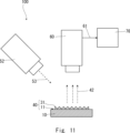
- the interfacial fracture rate measuring device 100 of the first embodiment includes a UV light source section 52 that irradiates UV light 53 to the adhesive fracture surface 40, and an imaging section that images the fluorescence 42 emitted by the adhesive residue 31 on the adhesive fracture surface 40. 60, and an image processing means 70 that determines the site of interface destruction from the captured image 61 and calculates its area ratio.
- the interfacial destruction rate measuring device focuses on the fact that many adhesives contain components that emit fluorescence, and identifies the interfacial destruction site based on the correlation between the thickness of the adhesive residue and the fluorescence intensity. It is something. That is, the fluorescence of the adhesive fracture surface is imaged, the light intensity (fluorescence intensity) at each pixel of the obtained image is analyzed, and the form of fracture at the position of the fracture surface corresponding to the pixel is determined according to the light intensity. At least the interfacial failure site, preferably the thin layer cohesive failure site, and the area ratio of the cohesive failure site are calculated.
- the UV (ultraviolet) light source section 52 may include at least a light source that emits UV light. Examples of the light source include a UV lamp and a UV-LED.
- the UV light source unit 52 may be configured with only a UV light source, but in order to improve measurement accuracy, it is preferable to include a high-pass filter that cuts visible light on the optical path between the UV light source and the adhesive fracture surface. . There may be one UV light source section 52, or a plurality of UV light source sections 52 may be provided depending on the shape of the broken adhesive surface.
- a visible light source section may be further provided (not shown).
- the visible light source is not particularly limited, and known light sources such as LEDs and fluorescent lights can be used.
- the imaging unit 60 may include at least a camera that images the fluorescence of the adhesive fracture surface.
- a digital camera is preferred because it can be easily incorporated into the image processing means. Further, when imaging only fluorescence, a monochrome camera is preferable. On the other hand, when capturing a visible light image of the adhesive fracture surface, a color digital camera is preferable.
- the imaging unit 60 may be configured with only a camera, but in order to improve measurement accuracy, it is preferable to include a low-pass filter that cuts UV light on the optical path between the adhesive fracture surface and the camera.
- the image processing means 70 is as described above.
- FIG. 7 is a flowchart illustrating an example of the interfacial fracture rate measuring method according to the first embodiment.
- the interfacial fracture rate measuring method according to the present embodiment includes at least a step of preparing an article having an adhesive fracture surface to be measured (S10), a step of imaging fluorescence of the adhesive fracture surface (S20), and a step of imaging the fluorescence of the adhesive fracture surface.
- the method includes a calculation step (S30) of calculating the area ratio of interface destruction from the obtained image.
- an article having an adhesive fracture surface to be measured is prepared.
- the article is a sample used for a product quality control test or a test for improving the adhesive part of a product
- the first adherend 10 the adhesive layer 30, as shown in the example of FIG.
- peeling is performed using a predetermined method to prepare an adhesive fracture surface.
- the predetermined method may be based on, for example, various peel test methods specified in JIS, or may be any method determined by the tester.
- the bonded parts of the products used may deteriorate over time or under certain environments and peel off.
- Masking may be performed on the periphery of the adhesive fracture surface to be measured. By masking, the range of the image can be easily identified. It is preferable that a masking material that does not emit fluorescence is appropriately selected and used.
- the sample is fixed and irradiated with UV light, and fluorescence is imaged (S20).
- the sample temperature during imaging be constant.
- the temperature can be controlled by keeping the sample holder at a constant temperature or by controlling the environmental temperature to a constant level.
- the imaging unit 60 or the sample holder may be moved to capture images continuously or intermittently. In this case, the images are combined in the image processing means 70. Note that it is usually preferable to perform the measurement in a dark place.
- the example shown in FIG. 8 is a method for determining the locations of interfacial failure, thin layer cohesive failure, and cohesive failure.
- the light intensity In at pixel n of the image is referred to (S31).
- a pixel here is the smallest unit of an image in an image obtained as digital data.
- the light intensity In is compared with a predetermined value A (S32). If it is less than the predetermined value A, it is determined that the fracture state of the portion of the adhesive fracture surface corresponding to the pixel n is an interface fracture.
- the light intensity In is greater than or equal to the predetermined value A, it is further compared with another predetermined value B (S33). If it is less than the predetermined value B, it is determined that the failure state of the portion of the adhesive fracture surface corresponding to the pixel n is thin-layer cohesive failure. If the light intensity In is equal to or greater than the predetermined value B, it is determined that the fracture state of the portion of the adhesive fracture surface corresponding to the pixel n is cohesive failure. This process is performed for all pixels to calculate the area of interface failure (number of pixels), area of thin layer cohesive failure (number of pixels), and area of cohesive failure (number of pixels), and calculate the area ratio from these values. Calculate the interface failure rate.
- the predetermined value A and the predetermined value B are set in advance.
- the predetermined value A is a threshold for interfacial failure and thin layer cohesive failure.
- the predetermined value A was obtained by preparing a sample of the first adherend 10 or the second adherend 20 and performing a measurement similar to the present interfacial fracture rate measuring method on the surface of the adherend. It can be determined from the fluorescence intensity.
- the predetermined value B is a threshold value for thin layer cohesive failure and cohesive failure. At present, a quantitative definition of thin-layer cohesive failure has not been determined, and it may be set as appropriate depending on the purpose of the sample, the thickness of the adhesive layer 30, etc.
- a case where the thickness of the adhesive residue is 1 ⁇ m or less may be determined to be thin-layer cohesive failure, and for example, a case where the thickness of the adhesive residue is 1/10 or less of the thickness of the original adhesive layer 30. It may be determined that this is a thin layer cohesive failure. If the thickness of the adhesive residue is 1 ⁇ m or less is defined as thin-layer cohesive failure, the adhesive is applied to the first adherend 10 to a thickness of 1 ⁇ m, and if necessary, cured to a predetermined value. It may be determined from the fluorescence intensity obtained by preparing a sample for B determination and performing a measurement similar to the present interfacial destruction rate measuring method on the sample.
- FIG. 9 shows an example of image processing of an image of an adhesive fracture surface using the interfacial fracture rate measuring device and interfacial fracture rate measuring method of Embodiment 1.
- FIG. 10 shows a visible light image of the same adhesive fracture surface as FIG. 9.
- the example in FIG. 9 is an image of an adhesive fracture surface divided into interfacial failure 32, thin layer cohesive failure 34, and cohesive failure 33 in S30 described above.
- FIG. 9 it can be seen that in the area surrounded by the dotted line in FIG. 10, it is difficult to distinguish between the interfacial failure 32 and the thin layer cohesive failure 34 using visible light.
- the interfacial fracture 32 and the thin layer cohesive fracture 34 are clearly distinguished by the interfacial fracture rate measurement method of the first embodiment.
- the interfacial fracture rate measuring device and the interfacial fracture rate measuring method of the first embodiment it is possible to measure interfacial fracture, thin layer cohesive failure, and cohesive failure with high accuracy.
- the present invention is not limited to the above-described Embodiment 1.
- a modification of the first embodiment described above will be described below. Note that two or more modified examples may be applied in combination to the first embodiment.
- the adhesive fracture surface formed by peeling off the adhesive part is the first adhesive fracture surface on the first adherend 10 side and the opposing second adhesive fracture surface on the second adherend 20 side. It is formed by a set of two second adhesion fracture surfaces. From the viewpoint of improving the accuracy of identifying the morphology of the fractured surface, it is necessary to image not only the cross section of one adhesive, but also the fluorescence of the first adhesive fractured surface and the fluorescence of the opposing second adhesive fractured surface, and perform image processing on each. It is preferable to do so.
- the first adherend or the second adherend is made of a material that emits fluorescence, not only the adhesive residue but also the adherend emits fluorescence when UV light is irradiated.
- a hyperspectral camera or a multispectral camera is used to capture an image containing wavelength information, and the image processing means 70 uses fluorescence intensity in a wavelength range where the influence of fluorescence derived from the adherend is small, allowing for highly accurate measurement. becomes possible.
- Fluorescence intensity may be low in thin layer cohesive failure areas.
- lock-in processing, high dynamic range processing, etc. may be performed.
- a modulation signal is created using a computer, and while modulating the illuminance of UV light at a predetermined modulation frequency corresponding to this signal, the imaging unit 60 emits the fluorescence for a predetermined period of time.
- images are taken continuously or intermittently, lock-in processing is performed using the predetermined modulation frequency of the modulation signal as a reference frequency in the image processing means 70, and areas such as interface destruction are detected based on the fluorescence intensity of the image subjected to the lock-in processing.
- This method noise can be significantly reduced and fluorescence sensitivity can be improved. Further, according to this method, it is possible to capture fluorescence even when the present interfacial destruction rate measuring device is used in a bright place.
- the high dynamic range processing uses a unit capable of adjusting the illuminance of UV light as the UV light source section 52, and captures a plurality of images with the imaging section 60 under different conditions of UV light illuminance.
- a method in which the plurality of images are combined by high dynamic range processing in the image processing means 70 and the site of interface destruction is determined based on the fluorescence intensity of the high dynamic range processed image.
- the measurement range of fluorescence intensity can be expanded, and for example, even when the adhesive contains components with high fluorescence intensity or when the adhesive layer is thick, thin-layer cohesive failure can be detected. Can be detected with high precision.
- a scanning type device may be used.
- the UV light source section 52 has a first optical fiber that emits UV light
- the imaging section 60 has a second optical fiber that receives fluorescence
- the first optical fiber and the second optical fiber are connected to each other.
- An example of this method is to image the fluorescence emitted by the adhesive residue on the adhesive fracture surface by operating the adhesive.
- Using a scanning type device also improves the accuracy of determining the minute fracture state of the adhesive fracture surface.
- an interfacial destruction rate measuring device including a confocal optical system may be used.
- a highly directional light source such as a laser diode
- an objective lens is provided on the optical path from the UV light source section 52 to the bond fracture surface.
- a more specific example is a method of providing an optical system similar to a known confocal microscope.
- the imaging unit 60 when the first adherend and the second adherend have a three-dimensional shape such as a curved surface, it is preferable to use a three-dimensional camera as the imaging unit 60.
- the three-dimensional camera include a stereo system, a ToF system, and a structured illumination system.
- the present interfacial destruction rate measuring device and interfacial failure rate measuring method require that the adhesive contain a material that emits fluorescence. Although many adhesive components emit fluorescence, for example, some urethane adhesives do not emit fluorescence. In this case, by adding a small amount of fluorescent substance to the urethane adhesive as the adhesive component, the adhesive can be made applicable to this device. Note that if the fluorescent substance is contained in a small amount, an adhesive composition that emits fluorescence can be obtained without impairing the performance of the adhesive.
- FIG. 12 is a schematic diagram showing an example of an interface fracture rate measuring device 200 according to the second embodiment.
- the interface failure rate measuring device 200 of the second embodiment includes a polarized light source unit 54 that irradiates the adhesive fracture surface 40 with polarized light 55, and an imaging device that images the transmitted light 43 that has passed through the adhesive residue 31 on the adhesive fracture surface 40. 63 and an image processing means 70.
- the imaging unit 63 includes a polarizing plate 82 on the optical path of the transmitted light 43.
- the interfacial rupture rate measuring device focuses on the fact that polymeric materials constituting adhesives often have birefringence characteristics, and it is possible to find a correlation between the thickness of adhesive residue and the polarization characteristics of transmitted light. It was completed with the intention of being seen.
- the transmitted light transmitted through the adhesive fracture surface is imaged, the light intensity at each pixel of the obtained image is analyzed, and the form of fracture at the position of the fracture surface corresponding to the pixel is identified according to the light intensity.
- at least the area ratio of the interfacial failure site, preferably the thin layer cohesive failure site, and the cohesive failure site is calculated.
- the polarized light source section 54 may have any configuration as long as it can irradiate the adhesive fracture surface 40 with polarized light.
- it may be configured with only a polarized light source such as a polarized laser, a combination of a non-polarized light source and a polarizing plate, or a combination of a non-polarized light source and a polarization modulator.
- the non-polarized light source is not particularly limited, and known light sources such as LEDs and fluorescent lamps can be used.
- a polarizing plate and a polarization modulator are provided on the optical path between the light source and the adhesive fracture surface. Further, when capturing a visible light image (non-polarized light) of the adhesive fracture surface, a visible light source section may be further provided (not shown).
- the camera 62 of the imaging unit 63 is preferably a digital camera because it can be easily imported into the image processing means.
- Examples of the polarizing plate 82 include a quarter wavelength plate.
- the arrangement of the imaging section 63 is adjusted as appropriate depending on the material of the adherend 10 and the like. For example, when the adherend 10 is made of a highly light-reflective material such as metal, the imaging section 63 is arranged so as to image the transmitted light 43 reflected by the interface 11, as shown in the example of FIG. Further, when the adherend 10 has low transparency such as a transparent film, the imaging section 63 is arranged to image the transmitted light 43 that has passed through the adhesive residue 31 and the adherend 10 (not shown).
- the preparation step (S10) and the imaging step (S20) are as described in the first embodiment.
- UV light should be read as polarized light
- fluorescence should be read as transmitted light.
- the area ratio calculation step (S30) will be explained.
- the traveling direction of light is the X axis
- the plane perpendicular to the X axis is the YZ plane.
- the polarized light 55 is linearly polarized light in the Z-axis direction.
- the transmitted light 43 becomes elliptically polarized light.
- the major axis direction of the elliptically polarized light depends on the thickness of the adhesive residue 31.
- the Z-axis direction component of the transmitted light 43 is cut off, and light 83 corresponding to the Y-axis direction component enters the camera 62 .
- the intensity of light incident on the camera 62 changes depending on the thickness of the adhesive residue 31. Note that the correlation between the thickness of the adhesive residue 31 and the light intensity is not necessarily a linear correlation.
- FIG. 14 A specific example of the area ratio calculation step (S30) will be described with reference to FIG. 14.
- the example shown in FIG. 14 is a method in which the locations of interfacial failure, thin layer cohesive failure, and cohesive failure are determined by the crossed Nicol method, and the polarizing light 55 and the polarizing plate 82 are not rotated.
- the light intensity In at pixel n of the image is referred to (S41).
- the light intensity In is compared with a predetermined numerical value range C (S42). If In is within the predetermined numerical range C, it is determined that the fracture state of the portion of the adhesive fracture surface corresponding to the pixel n is an interface fracture.
- the light intensity In is outside the predetermined numerical value range C, it is further compared with another predetermined numerical value range D (S43). If In is within the predetermined numerical value range D, it is determined that the failure state of the portion of the adhesive fracture surface corresponding to the pixel n is thin-layer cohesive failure. If the light intensity In is outside the predetermined numerical value range D, it is determined that the fracture state of the portion of the adhesive fracture surface corresponding to the pixel n is cohesive failure. This process is performed for all pixels to calculate the area of interface failure (number of pixels), area of thin layer cohesive failure (number of pixels), and area of cohesive failure (number of pixels), and calculate the area ratio from these values. Calculate the interface failure rate.
- the predetermined numerical ranges C and D are set in advance.
- the predetermined numerical range C is a range of light intensity that indicates interfacial failure
- the predetermined numerical range D is a range of light intensity that indicates thin layer cohesive failure.
- One setting method is to prepare the same type of adhesive as the adhesive to be measured, form a coating film of multiple thicknesses, measure the light intensity of each in the same manner as above, and create a database. . Furthermore, if the birefringence characteristics of the adhesive are known, the relationship between the thickness and light intensity may be calculated and compiled into a database.
- FIG. 15 Another specific example of the area ratio calculation step (S30) will be described with reference to FIG. 15.
- images are captured while either the linearly polarized light 55 of the light source or the polarizing plate 82 is rotated at a predetermined speed. This causes the light intensity to change periodically.
- the difference in thickness of the adhesive residue 31 can be determined, and thereby the sites of interfacial failure, thin layer cohesive failure, and cohesive failure are determined. Note that in Figure 15, for clarity of explanation, we focus on two points, but by using three or more points, multiple phase information can be obtained, and the locations of interfacial failure, thin layer cohesive failure, and cohesive failure can be determined. becomes easier.
- a method for rotating the linearly polarized light 55 includes, for example, using a combination of a non-polarized light source and a polarizing plate as the polarized light source section 54 and rotating the polarizing plate.
- lock-in processing may be performed using a frequency based on the rotational speed of the linearly polarized light 55 or the polarizing plate 82 as a reference frequency, and the site of interface destruction may be determined based on the phase difference of the image subjected to the lock-in processing.
- Lock-in processing can significantly reduce noise and improve the accuracy of determining the locations of interfacial failure, thin layer cohesive failure, and cohesive failure.
- the present invention is not limited to the above-mentioned Embodiment 2.
- Modifications of the second embodiment include Modification 1 and Modifications 3 to 6 described in the first embodiment. Note that the second embodiment may be applied in combination with two or more modified examples.
Landscapes
- Physics & Mathematics (AREA)
- Health & Medical Sciences (AREA)
- Life Sciences & Earth Sciences (AREA)
- Chemical & Material Sciences (AREA)
- Analytical Chemistry (AREA)
- Biochemistry (AREA)
- General Health & Medical Sciences (AREA)
- General Physics & Mathematics (AREA)
- Immunology (AREA)
- Pathology (AREA)
- Investigating, Analyzing Materials By Fluorescence Or Luminescence (AREA)
Priority Applications (2)
| Application Number | Priority Date | Filing Date | Title |
|---|---|---|---|
| EP23846600.7A EP4563973A1 (en) | 2022-07-28 | 2023-07-27 | Interface failure rate measurement device and interface failure rate measurement method |
| JP2024537213A JPWO2024024870A1 (https=) | 2022-07-28 | 2023-07-27 |
Applications Claiming Priority (2)
| Application Number | Priority Date | Filing Date | Title |
|---|---|---|---|
| JP2022120200 | 2022-07-28 | ||
| JP2022-120200 | 2022-07-28 |
Publications (1)
| Publication Number | Publication Date |
|---|---|
| WO2024024870A1 true WO2024024870A1 (ja) | 2024-02-01 |
Family
ID=89706553
Family Applications (1)
| Application Number | Title | Priority Date | Filing Date |
|---|---|---|---|
| PCT/JP2023/027482 Ceased WO2024024870A1 (ja) | 2022-07-28 | 2023-07-27 | 界面破壊率測定装置、及び界面破壊率測定方法 |
Country Status (3)
| Country | Link |
|---|---|
| EP (1) | EP4563973A1 (https=) |
| JP (1) | JPWO2024024870A1 (https=) |
| WO (1) | WO2024024870A1 (https=) |
Cited By (1)
| Publication number | Priority date | Publication date | Assignee | Title |
|---|---|---|---|---|
| EP4675261A1 (de) * | 2024-07-04 | 2026-01-07 | Schäfter + Kirchhoff GmbH | Verfahren und vorrichtung für eine bruchflächenanalyse |
Citations (9)
| Publication number | Priority date | Publication date | Assignee | Title |
|---|---|---|---|---|
| JPH05331438A (ja) * | 1992-05-30 | 1993-12-14 | Sony Corp | 蛍光性接着剤及び接着剤の塗布状態検査方法、検査装置 |
| JPH08327498A (ja) * | 1995-03-27 | 1996-12-13 | Unie Opt:Kk | 複屈折測定装置 |
| JP2001091850A (ja) * | 1999-09-20 | 2001-04-06 | Olympus Optical Co Ltd | 走査型レーザ顕微鏡 |
| JP2002000548A (ja) * | 2001-07-02 | 2002-01-08 | Olympus Optical Co Ltd | 内視鏡装置 |
| JP2018059736A (ja) | 2016-10-03 | 2018-04-12 | アズビル株式会社 | 接合基板、接合基板の検査方法、および半導体デバイスの製造方法。 |
| JP2018181204A (ja) * | 2017-04-20 | 2018-11-15 | 国立大学法人秋田大学 | 対象物推定装置 |
| WO2021193609A1 (ja) * | 2020-03-24 | 2021-09-30 | 三菱ケミカル株式会社 | 繊維強化複合材および接合体 |
| JP2022107877A (ja) * | 2021-01-12 | 2022-07-25 | パナソニックIpマネジメント株式会社 | 部品撮像装置および部品実装装置 |
| JP2022120200A (ja) | 2019-01-31 | 2022-08-17 | ファイザー・インク | Cdk2阻害剤 |
-
2023
- 2023-07-27 JP JP2024537213A patent/JPWO2024024870A1/ja active Pending
- 2023-07-27 WO PCT/JP2023/027482 patent/WO2024024870A1/ja not_active Ceased
- 2023-07-27 EP EP23846600.7A patent/EP4563973A1/en active Pending
Patent Citations (9)
| Publication number | Priority date | Publication date | Assignee | Title |
|---|---|---|---|---|
| JPH05331438A (ja) * | 1992-05-30 | 1993-12-14 | Sony Corp | 蛍光性接着剤及び接着剤の塗布状態検査方法、検査装置 |
| JPH08327498A (ja) * | 1995-03-27 | 1996-12-13 | Unie Opt:Kk | 複屈折測定装置 |
| JP2001091850A (ja) * | 1999-09-20 | 2001-04-06 | Olympus Optical Co Ltd | 走査型レーザ顕微鏡 |
| JP2002000548A (ja) * | 2001-07-02 | 2002-01-08 | Olympus Optical Co Ltd | 内視鏡装置 |
| JP2018059736A (ja) | 2016-10-03 | 2018-04-12 | アズビル株式会社 | 接合基板、接合基板の検査方法、および半導体デバイスの製造方法。 |
| JP2018181204A (ja) * | 2017-04-20 | 2018-11-15 | 国立大学法人秋田大学 | 対象物推定装置 |
| JP2022120200A (ja) | 2019-01-31 | 2022-08-17 | ファイザー・インク | Cdk2阻害剤 |
| WO2021193609A1 (ja) * | 2020-03-24 | 2021-09-30 | 三菱ケミカル株式会社 | 繊維強化複合材および接合体 |
| JP2022107877A (ja) * | 2021-01-12 | 2022-07-25 | パナソニックIpマネジメント株式会社 | 部品撮像装置および部品実装装置 |
Cited By (1)
| Publication number | Priority date | Publication date | Assignee | Title |
|---|---|---|---|---|
| EP4675261A1 (de) * | 2024-07-04 | 2026-01-07 | Schäfter + Kirchhoff GmbH | Verfahren und vorrichtung für eine bruchflächenanalyse |
Also Published As
| Publication number | Publication date |
|---|---|
| JPWO2024024870A1 (https=) | 2024-02-01 |
| EP4563973A1 (en) | 2025-06-04 |
Similar Documents
| Publication | Publication Date | Title |
|---|---|---|
| JP7504189B2 (ja) | 膜厚測定装置及び膜厚測定方法 | |
| CN102349017B (zh) | 焦点信息生成设备和焦点信息生成方法 | |
| KR100988454B1 (ko) | 두께 측정방법 | |
| WO2009116359A1 (ja) | 接触面積測定装置および接触面積測定方法 | |
| US7872741B2 (en) | Method and apparatus for scatterfield microscopical measurement | |
| WO2024024870A1 (ja) | 界面破壊率測定装置、及び界面破壊率測定方法 | |
| JP7374815B2 (ja) | 検査方法 | |
| KR100876257B1 (ko) | 광학적 측정 방법 및 그 장치 | |
| JP2009145141A (ja) | 欠陥検査装置及び欠陥検査プログラム | |
| CN111601051B (zh) | 一种对准图像获取方法、装置及系统 | |
| JP7838942B2 (ja) | 検査方法 | |
| US20030170732A1 (en) | Liquid-containing substance analyzing device and liquid-containing substance analyzing method | |
| JP2006194800A (ja) | 研磨加工測定方法及び研磨装置 | |
| JP2003083886A (ja) | 表面プラズモン顕微鏡及び表面プラズモン顕微鏡における暗環像情報取得方法 | |
| JP2002062218A (ja) | 光学的異方性物質評価装置 | |
| JP6940302B2 (ja) | 欠陥検査装置及び欠陥検査方法 | |
| KR20070091236A (ko) | 결함 입자 측정 장치 및 결함 입자 측정 방법 | |
| US20210255115A1 (en) | Foreign material inspection system of display unit | |
| JP3141470B2 (ja) | 3次元形状検出方法および装置 | |
| KR100662576B1 (ko) | 광학디바이스의 검사장치 및 검사방법 | |
| US7154601B2 (en) | Testing method for a polarizing plate | |
| JP2020518812A (ja) | 微小散乱測定システム、及びその使用方法 | |
| KR102241104B1 (ko) | 편광 정렬 검사 장치 및 그 검사 방법 | |
| WO2026070363A1 (ja) | 異物検査装置、及び異物検査方法 | |
| WO2026069603A1 (ja) | 光学検査装置及びその制御方法 |
Legal Events
| Date | Code | Title | Description |
|---|---|---|---|
| 121 | Ep: the epo has been informed by wipo that ep was designated in this application |
Ref document number: 23846600 Country of ref document: EP Kind code of ref document: A1 |
|
| WWE | Wipo information: entry into national phase |
Ref document number: 2024537213 Country of ref document: JP |
|
| WWE | Wipo information: entry into national phase |
Ref document number: 2023846600 Country of ref document: EP |
|
| NENP | Non-entry into the national phase |
Ref country code: DE |
|
| ENP | Entry into the national phase |
Ref document number: 2023846600 Country of ref document: EP Effective date: 20250228 |
|
| WWP | Wipo information: published in national office |
Ref document number: 2023846600 Country of ref document: EP |