WO2024024386A1 - 半導体装置および半導体装置の製造方法 - Google Patents
半導体装置および半導体装置の製造方法 Download PDFInfo
- Publication number
- WO2024024386A1 WO2024024386A1 PCT/JP2023/024274 JP2023024274W WO2024024386A1 WO 2024024386 A1 WO2024024386 A1 WO 2024024386A1 JP 2023024274 W JP2023024274 W JP 2023024274W WO 2024024386 A1 WO2024024386 A1 WO 2024024386A1
- Authority
- WO
- WIPO (PCT)
- Prior art keywords
- hydrogen
- region
- semiconductor device
- layer
- conductivity type
- Prior art date
- Legal status (The legal status is an assumption and is not a legal conclusion. Google has not performed a legal analysis and makes no representation as to the accuracy of the status listed.)
- Ceased
Links
Images







Classifications
-
- H—ELECTRICITY
- H10—SEMICONDUCTOR DEVICES; ELECTRIC SOLID-STATE DEVICES NOT OTHERWISE PROVIDED FOR
- H10D—INORGANIC ELECTRIC SEMICONDUCTOR DEVICES
- H10D62/00—Semiconductor bodies, or regions thereof, of devices having potential barriers
- H10D62/80—Semiconductor bodies, or regions thereof, of devices having potential barriers characterised by the materials
- H10D62/83—Semiconductor bodies, or regions thereof, of devices having potential barriers characterised by the materials being Group IV materials, e.g. B-doped Si or undoped Ge
- H10D62/834—Semiconductor bodies, or regions thereof, of devices having potential barriers characterised by the materials being Group IV materials, e.g. B-doped Si or undoped Ge further characterised by the dopants
-
- H—ELECTRICITY
- H10—SEMICONDUCTOR DEVICES; ELECTRIC SOLID-STATE DEVICES NOT OTHERWISE PROVIDED FOR
- H10P—GENERIC PROCESSES OR APPARATUS FOR THE MANUFACTURE OR TREATMENT OF DEVICES COVERED BY CLASS H10
- H10P30/00—Ion implantation into wafers, substrates or parts of devices
- H10P30/20—Ion implantation into wafers, substrates or parts of devices into semiconductor materials, e.g. for doping
- H10P30/202—Ion implantation into wafers, substrates or parts of devices into semiconductor materials, e.g. for doping characterised by the semiconductor materials
- H10P30/204—Ion implantation into wafers, substrates or parts of devices into semiconductor materials, e.g. for doping characterised by the semiconductor materials into Group IV semiconductors
-
- H—ELECTRICITY
- H10—SEMICONDUCTOR DEVICES; ELECTRIC SOLID-STATE DEVICES NOT OTHERWISE PROVIDED FOR
- H10D—INORGANIC ELECTRIC SEMICONDUCTOR DEVICES
- H10D12/00—Bipolar devices controlled by the field effect, e.g. insulated-gate bipolar transistors [IGBT]
-
- H—ELECTRICITY
- H10—SEMICONDUCTOR DEVICES; ELECTRIC SOLID-STATE DEVICES NOT OTHERWISE PROVIDED FOR
- H10D—INORGANIC ELECTRIC SEMICONDUCTOR DEVICES
- H10D30/00—Field-effect transistors [FET]
- H10D30/01—Manufacture or treatment
- H10D30/021—Manufacture or treatment of FETs having insulated gates [IGFET]
- H10D30/028—Manufacture or treatment of FETs having insulated gates [IGFET] of double-diffused metal oxide semiconductor [DMOS] FETs
- H10D30/0291—Manufacture or treatment of FETs having insulated gates [IGFET] of double-diffused metal oxide semiconductor [DMOS] FETs of vertical DMOS [VDMOS] FETs
- H10D30/0297—Manufacture or treatment of FETs having insulated gates [IGFET] of double-diffused metal oxide semiconductor [DMOS] FETs of vertical DMOS [VDMOS] FETs using recessing of the gate electrodes, e.g. to form trench gate electrodes
-
- H—ELECTRICITY
- H10—SEMICONDUCTOR DEVICES; ELECTRIC SOLID-STATE DEVICES NOT OTHERWISE PROVIDED FOR
- H10D—INORGANIC ELECTRIC SEMICONDUCTOR DEVICES
- H10D30/00—Field-effect transistors [FET]
- H10D30/60—Insulated-gate field-effect transistors [IGFET]
- H10D30/64—Double-diffused metal-oxide semiconductor [DMOS] FETs
- H10D30/66—Vertical DMOS [VDMOS] FETs
- H10D30/668—Vertical DMOS [VDMOS] FETs having trench gate electrodes, e.g. UMOS transistors
-
- H—ELECTRICITY
- H10—SEMICONDUCTOR DEVICES; ELECTRIC SOLID-STATE DEVICES NOT OTHERWISE PROVIDED FOR
- H10D—INORGANIC ELECTRIC SEMICONDUCTOR DEVICES
- H10D62/00—Semiconductor bodies, or regions thereof, of devices having potential barriers
- H10D62/10—Shapes, relative sizes or dispositions of the regions of the semiconductor bodies; Shapes of the semiconductor bodies
-
- H—ELECTRICITY
- H10—SEMICONDUCTOR DEVICES; ELECTRIC SOLID-STATE DEVICES NOT OTHERWISE PROVIDED FOR
- H10D—INORGANIC ELECTRIC SEMICONDUCTOR DEVICES
- H10D62/00—Semiconductor bodies, or regions thereof, of devices having potential barriers
- H10D62/10—Shapes, relative sizes or dispositions of the regions of the semiconductor bodies; Shapes of the semiconductor bodies
- H10D62/13—Semiconductor regions connected to electrodes carrying current to be rectified, amplified or switched, e.g. source or drain regions
- H10D62/149—Source or drain regions of field-effect devices
- H10D62/151—Source or drain regions of field-effect devices of IGFETs
- H10D62/156—Drain regions of DMOS transistors
- H10D62/157—Impurity concentrations or distributions
-
- H—ELECTRICITY
- H10—SEMICONDUCTOR DEVICES; ELECTRIC SOLID-STATE DEVICES NOT OTHERWISE PROVIDED FOR
- H10P—GENERIC PROCESSES OR APPARATUS FOR THE MANUFACTURE OR TREATMENT OF DEVICES COVERED BY CLASS H10
- H10P30/00—Ion implantation into wafers, substrates or parts of devices
- H10P30/20—Ion implantation into wafers, substrates or parts of devices into semiconductor materials, e.g. for doping
- H10P30/208—Ion implantation into wafers, substrates or parts of devices into semiconductor materials, e.g. for doping of electrically inactive species
-
- H—ELECTRICITY
- H10—SEMICONDUCTOR DEVICES; ELECTRIC SOLID-STATE DEVICES NOT OTHERWISE PROVIDED FOR
- H10D—INORGANIC ELECTRIC SEMICONDUCTOR DEVICES
- H10D30/00—Field-effect transistors [FET]
- H10D30/01—Manufacture or treatment
- H10D30/021—Manufacture or treatment of FETs having insulated gates [IGFET]
- H10D30/028—Manufacture or treatment of FETs having insulated gates [IGFET] of double-diffused metal oxide semiconductor [DMOS] FETs
- H10D30/0291—Manufacture or treatment of FETs having insulated gates [IGFET] of double-diffused metal oxide semiconductor [DMOS] FETs of vertical DMOS [VDMOS] FETs
-
- H—ELECTRICITY
- H10—SEMICONDUCTOR DEVICES; ELECTRIC SOLID-STATE DEVICES NOT OTHERWISE PROVIDED FOR
- H10D—INORGANIC ELECTRIC SEMICONDUCTOR DEVICES
- H10D62/00—Semiconductor bodies, or regions thereof, of devices having potential barriers
- H10D62/80—Semiconductor bodies, or regions thereof, of devices having potential barriers characterised by the materials
- H10D62/83—Semiconductor bodies, or regions thereof, of devices having potential barriers characterised by the materials being Group IV materials, e.g. B-doped Si or undoped Ge
- H10D62/832—Semiconductor bodies, or regions thereof, of devices having potential barriers characterised by the materials being Group IV materials, e.g. B-doped Si or undoped Ge being Group IV materials comprising two or more elements, e.g. SiGe
- H10D62/8325—Silicon carbide
Definitions
- the present invention relates to a semiconductor device and a method for manufacturing a semiconductor device.
- SiC Silicon carbide
- SiC semiconductor devices it is known that when a current is applied, injected carriers are trapped in stacking faults in an epitaxial layer, lowering the stacking fault energy and leading to expansion of the stacking faults. The expansion of stacking faults is viewed as an issue because it leads to an increase in forward voltage.
- One exemplary object of an embodiment of the present invention is to provide a technique for suppressing the expansion of stacking faults during current application to a SiC semiconductor device.
- a method for manufacturing a semiconductor device includes irradiating a semiconductor device including a substrate made of silicon carbide and a semiconductor layer of a first conductivity type on a first surface of the substrate with hydrogen ions to form a semiconductor device of 1 ⁇ m or more.
- the method includes forming a high hydrogen concentration region having a hydrogen concentration exceeding 10 15 /cm 3 over the thickness. At least a portion of the high concentration hydrogen region is formed within the first conductivity type semiconductor layer.
- This semiconductor device includes a substrate made of silicon carbide, a semiconductor layer of a first conductivity type provided on the substrate, and a high concentration hydrogen region having a hydrogen concentration exceeding 10 15 /cm 3 over a thickness of 1 ⁇ m or more. . At least a portion of the high concentration hydrogen region is formed within the first conductivity type semiconductor layer.
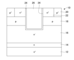
- FIG. 1 is a cross-sectional view schematically showing a configuration example of a semiconductor device according to an embodiment.
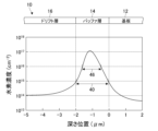
- 3 is a graph showing an example of the hydrogen concentration of a semiconductor device after hydrogen ion irradiation. It is a table showing the thickness of the high concentration hydrogen region and the presence or absence of expansion of stacking faults in comparative examples and examples.
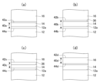
- FIG. 7 is a diagram schematically showing another example of the formation position of a high concentration hydrogen region.
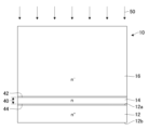
- FIG. 1 is a cross-sectional view schematically showing a manufacturing process of a semiconductor device.
- FIG. 3 is a cross-sectional view schematically showing a manufacturing process of a semiconductor device.
- FIG. 1 is a cross-sectional view schematically showing a manufacturing process of a semiconductor device.
- FIG. 1 is a cross-sectional view schematically showing a manufacturing process of a semiconductor device.
- FIG. 1 is a cross-sectional view schematically showing a manufacturing process of a semiconductor device.
- FIG. 1 is a cross-sectional view schematically showing a manufacturing process of a semiconductor device.
- FIG. 1 is a cross-sectional view schematically showing a manufacturing process of a semiconductor device.
- FIG. 1 is a cross-sectional view schematically showing a manufacturing process of a semiconductor device.
- 3 is a flowchart illustrating an example of a method for manufacturing a semiconductor device according to an embodiment.
- This embodiment relates to a SiC semiconductor device including a substrate made of silicon carbide (SiC) and a semiconductor layer of a first conductivity type provided on a first surface of the substrate.
- SiC silicon carbide
- a problem with such SiC semiconductor devices is that stacking faults existing near the interface between the substrate and the semiconductor layer expand when a current is applied, leading to an increase in forward voltage.
- hydrogen ions are irradiated near the interface between the substrate and the semiconductor layer to fix hydrogen to partial dislocations surrounding stacking faults, thereby suppressing expansion of stacking faults when current is applied.
- fixing hydrogen to partial dislocations it is possible to suppress a decrease in stacking fault energy due to trapping of injected carriers in stacking faults.
- expansion of stacking faults can be suppressed by forming a high concentration hydrogen region having a hydrogen concentration of more than 10 15 /cm 3 over a thickness of 1 ⁇ m or more by irradiation with hydrogen ions.
- a highly concentrated hydrogen region with a thickness of 1 ⁇ m or more, a sufficient amount of hydrogen can be fixed to the partial dislocations that border the stacking faults that exist near the interface between the substrate and the semiconductor layer, and the stacking faults can be expanded. can be suitably suppressed.
- FIG. 1 is a cross-sectional view schematically showing a configuration example of a semiconductor device 10 according to an embodiment.
- the semiconductor device 10 is a SiC semiconductor device, and is a metal oxide semiconductor field effect transistor (MOSFET).
- the semiconductor device 10 includes a substrate 12, a buffer layer 14, a drift layer 16, a base region 18, a source region 20, a base contact region 22, a gate insulating film 24, a gate electrode 26, and an interlayer insulating film 28. , a source electrode 30 , and a drain electrode 32 .
- MOSFET metal oxide semiconductor field effect transistor
- the substrate 12 is a SiC substrate made of silicon carbide (SiC) of a first conductivity type (for example, n-type) or a second conductivity type (for example, p-type).
- the substrate 12 is, for example, an n-type SiC substrate, and is doped with, for example, nitrogen (N) as an n-type impurity.
- the impurity concentration of the first conductivity type or the second conductivity type of the substrate 12 is 1.0 ⁇ 10 18 /cm 3 or more, for example, 2.0 ⁇ 10 18 /cm 3 or more and 5.0 ⁇ 10 19 /cm 3 . It is as follows.
- the substrate 12 includes a first surface 12a and a second surface 12b opposite to the first surface 12a.
- the first surface 12a is, for example, a (0001) Si surface.
- Buffer layer 14 is a first conductivity type SiC semiconductor layer epitaxially grown on first surface 12 a of substrate 12 .
- the buffer layer 14 is, for example, an n-type SiC layer, and is doped with, for example, nitrogen (N) as an n-type impurity.
- the first conductivity type impurity concentration of the buffer layer 14 is lower than the first conductivity type or second conductivity type impurity concentration of the substrate 12 and higher than the first conductivity type impurity concentration of the drift layer 16 .
- the impurity concentration of the first conductivity type of the buffer layer 14 is, for example, 1.0 ⁇ 10 16 /cm 3 or more and 1.0 ⁇ 10 18 /cm 3 or less.
- the thickness of the buffer layer 14 is 1.0 ⁇ m or more and 5.0 ⁇ m or less, for example, 1.5 ⁇ m or more and 3.0 ⁇ m or less, and for example, 2.0 ⁇ m.
- Drift layer 16 is a first conductivity type SiC semiconductor layer epitaxially grown on buffer layer 14 .
- the drift layer 16 is, for example, an n-type SiC layer, and is doped with, for example, nitrogen (N) as an n-type impurity.
- the first conductivity type impurity concentration of the drift layer 16 is lower than the first conductivity type impurity concentration of the buffer layer 14 .
- the first conductivity type impurity concentration of the drift layer 16 is, for example, 1.0 ⁇ 10 15 /cm 3 or more and 1.0 ⁇ 10 17 /cm 3 or less.
- the thickness of the drift layer 16 is greater than the thickness of the buffer layer 14.
- the thickness of the drift layer 16 is 5.0 ⁇ m or more and 50 ⁇ m or less, for example, 7.5 ⁇ m or more and 15 ⁇ m or less, and is, for example, 10 ⁇ m.
- Base region 18 is a second conductivity type SiC semiconductor region provided on drift layer 16 .
- the base region 18 is, for example, a p-type, and is doped with, for example, aluminum (Al) as a p-type impurity.
- the base region 18 is formed, for example, by irradiating the drift layer 16 with impurity ions of the second conductivity type.
- the impurity concentration of the second conductivity type in the base region 18 is higher than the impurity concentration of the first conductivity type in the drift layer 16 .
- the second conductivity type impurity concentration of the base region 18 is, for example, 1.0 ⁇ 10 16 /cm 3 or more and 1.0 ⁇ 10 18 /cm 3 or less.
- Source region 20 is a first conductivity type SiC semiconductor region provided on base region 18 .
- Source region 20 is provided adjacent to gate insulating film 24 .
- the source region 20 is, for example, an n-type, and is doped with, for example, nitrogen (N) as an n-type impurity.
- the source region 20 is formed, for example, by irradiating the drift layer 16 with impurity ions of the first conductivity type.
- the impurity concentration of the first conductivity type in the source region 20 is higher than that in the drift layer 16 .
- the impurity concentration of the first conductivity type in the source region 20 is 1.0 ⁇ 10 18 /cm 3 or more, for example, 2.0 ⁇ 10 18 /cm 3 or more and 5.0 ⁇ 10 19 /cm 3 or less.
- Base contact region 22 is a second conductivity type SiC semiconductor region provided on base region 18 .
- Base contact region 22 is provided apart from gate insulating film 24 .
- the base contact region 22 is, for example, a p-type, and is doped with, for example, aluminum (Al) as a p-type impurity.
- the base contact region 22 is formed, for example, by irradiating the drift layer 16 with impurity ions of the second conductivity type.
- the second conductivity type impurity concentration of base contact region 22 is higher than the second conductivity type impurity concentration of base region 18 .
- the second conductivity type impurity concentration of the base contact region 22 is, for example, 1.0 ⁇ 10 17 /cm 3 or more and 1.0 ⁇ 10 19 /cm 3 or less.
- the gate insulating film 24 is provided on the inner wall surface of the gate trench 34. Gate insulating film 24 is provided adjacent to drift layer 16, base region 18, and source region 20.
- the gate trench 34 is formed so as to be dug from the upper surface 20a of the source region 20 toward the substrate 12. Gate trench 34 is formed to penetrate source region 20 and base region 18 and reach the top of drift layer 16 .
- the gate insulating film 24 is formed of an oxide material, for example SiO 2 .
- the gate electrode 26 is provided so as to fill the inside of the gate insulating film 24 (gate trench 34).
- the gate electrode 26 is formed of, for example, polycrystalline silicon doped with n-type impurities such as phosphorus (P) and nitrogen (N).
- the interlayer insulating film 28 is provided on the gate insulating film 24 and the gate electrode 26.
- Interlayer insulating film 28 is formed of any insulating material.
- the source electrode 30 is provided on the source region 20, base contact region 22, and interlayer insulating film 28. Source electrode 30 contacts upper surface 20a of source region 20 and upper surface 22a of base contact region 22.
- the source electrode 30 is made of a metal material such as chromium (Cr) or nickel (Ni), for example.
- the source electrode 30 may be formed of a metal multilayer film in which a plurality of metal layers made of different metal materials are laminated.
- the source electrode 30 is a surface metal electrode layer formed on the surface of the semiconductor device 10.
- the drain electrode 32 is provided on the second surface 12b of the substrate 12. Drain electrode 32 contacts second surface 12b of substrate 12.
- the drain electrode 32 is made of a metal material such as chromium (Cr) or nickel (Ni), for example.
- the drain electrode 32 may be formed of a metal multilayer film in which a plurality of metal layers made of different metal materials are laminated.
- the drain electrode 32 is a back metal electrode layer formed on the back surface of the semiconductor device 10.
- the semiconductor device 10 is irradiated with hydrogen ions, and a high concentration hydrogen region 40 having a hydrogen concentration exceeding 10 15 /cm 3 is formed over a thickness of 1 ⁇ m or more. At least a portion of the high concentration hydrogen region 40 is formed in the buffer layer 14 or the drift layer 16, which is a first conductivity type semiconductor layer. In the example of FIG. 1, the entire high concentration hydrogen region 40 is formed in the buffer layer 14, and the upper end 42 and lower end 44 of the high concentration hydrogen region 40 are located in the buffer layer 14.
- FIG. 2 is a graph showing an example of the hydrogen concentration of the semiconductor device 10 after hydrogen ion irradiation.
- FIG. 2 shows the case where the hydrogen ion irradiation energy was 960 keV and the dose was 1.0 ⁇ 10 13 /cm 2 .
- the thickness range of the high hydrogen concentration region 40 where the hydrogen concentration exceeds 10 15 /cm 3 is approximately 1.9 ⁇ m.
- the high hydrogen concentration region 40 has a hydrogen concentration greater than 10 16 /cm 3 in a thickness range 46 of approximately 1.1 ⁇ m.
- the peak value of the hydrogen concentration in the high hydrogen concentration region 40 is about 1.1 ⁇ 10 17 /cm 3 .
- the presence or absence of stacking fault expansion can be confirmed by an X-ray topography method or a photoluminescence method.
- FIG. 3 is a table showing the thickness of the high concentration hydrogen region 40 and the presence or absence of stacking fault expansion in the comparative example and the example.
- Figure 3 summarizes the presence or absence of stacking fault expansion when the hydrogen ion irradiation dose was varied in the range of 1.0 ⁇ 10 10 /cm 2 to 1.0 ⁇ 10 16 /cm 2 . .
- Comparative Examples 1 and 2 in which the thickness of the high concentration hydrogen region 40 was less than 1 ⁇ m, expansion of stacking faults was confirmed.
- Examples 1 to 5 in which the high concentration hydrogen region 40 had a thickness of 1 ⁇ m or more, no expansion of stacking faults was observed, indicating that expansion of stacking faults could be suppressed.
- FIGS. 4(a) to 4(d) are diagrams schematically showing other examples of formation positions of the high concentration hydrogen regions 40a to 40d.
- the high concentration hydrogen region 40a shown in FIG. 4(a) is formed across the substrate 12 and the buffer layer 14, and is formed across the first surface 12a, which is the interface between the substrate 12 and the buffer layer 14.
- An upper end 42a of the high concentration hydrogen region 40a is located on the buffer layer 14, and a lower end 44a of the high concentration hydrogen region 40a is located on the substrate 12.
- At least a portion of the high concentration hydrogen region 40a is formed in the substrate 12 and the buffer layer 14.
- the high concentration hydrogen region 40b shown in FIG. 4(b) is formed across the substrate 12, buffer layer 14, and drift layer 16.
- High concentration hydrogen region 40b is formed across first surface 12a, which is the interface between substrate 12 and buffer layer 14, and is also formed across interface 36 between buffer layer 14 and drift layer 16.
- the upper end 42b of the high concentration hydrogen region 40b is located on the drift layer 16, and the lower end 44b of the high concentration hydrogen region 40b is located on the substrate 12.
- At least a portion of high concentration hydrogen region 40b is formed in substrate 12, buffer layer 14, and drift layer 16.
- a high concentration hydrogen region 40c shown in FIG. 4(c) is formed across the buffer layer 14 and the drift layer 16.
- High concentration hydrogen region 40c is formed across interface 36 between buffer layer 14 and drift layer 16.
- the upper end 42c of the high concentration hydrogen region 40c is located in the drift layer 16
- the lower end 44c of the high concentration hydrogen region 40c is located in the buffer layer 14.
- At least a portion of the high concentration hydrogen region 40b is formed in the buffer layer 14 and the drift layer 16.
- the high concentration hydrogen region 40d shown in FIG. 4(d) is formed only in the drift layer 16.
- An upper end 42d and a lower end 44d of the high concentration hydrogen region 40d are located in the drift layer 16.
- the high concentration hydrogen regions 40, 40a to 40d are formed near the first surface 12a of the substrate 12. At least a portion of the high concentration hydrogen regions 40, 40a to 40d is preferably formed within 5 ⁇ m from the first surface 12a of the substrate 12.
- the upper ends 42, 42a-42d or the lower ends 44, 44a-44d of the high concentration hydrogen regions 40, 40a-40d are preferably located within 5 ⁇ m from the first surface 12a of the substrate 12.
- the upper ends 42, 42a-42d or the lower ends 44, 44a-44d of the high concentration hydrogen regions 40, 40a-40d may be formed within 4 ⁇ m, 3 ⁇ m, or 2 ⁇ m from the first surface 12a of the substrate 12.
- the hydrogen concentration in the high-concentration hydrogen regions 40, 40a to 40d may be reduced after the fact due to annealing treatment included in the manufacturing process of the semiconductor device 10. For example, if an annealing process is performed after irradiation with hydrogen ions, the annealing process may cause hydrogen to diffuse and reduce the hydrogen concentration. At this time, the hydrogen fixed to the partial dislocations surrounding the stacking faults remains fixed even after the annealing process. In other words, hydrogen diffused by the annealing process is not fixed to the partial dislocations surrounding the stacking faults, and is considered not to contribute to suppressing the expansion of the stacking faults.
- the buffer layer 14 or the drift layer 16 at the time of completion of the semiconductor device 10 is 1.0 ⁇ 10 15 /cm 2 or less, the buffer layer 14 or the drift layer 16 after hydrogen ion irradiation If the hydrogen concentration in the drift layer 16 exceeds 1.0 ⁇ 10 15 /cm 2 over a thickness of 1 ⁇ m or more, expansion of stacking faults can be suppressed.
- the hydrogen concentration in the buffer layer 14 or drift layer 16 of the semiconductor device 10 may remain in a state exceeding 1.0 ⁇ 10 15 /cm 2 .
- the high concentration hydrogen regions 40, 40a to 40d are formed by irradiation with hydrogen ions, expansion of stacking faults can be suppressed.
- 5 to 11 are cross-sectional views schematically showing the manufacturing process of a semiconductor device.
- the buffer layer 14 is formed on the first surface 12a of the substrate 12, and the drift layer 16 is formed on the buffer layer 14.
- Buffer layer 14 and drift layer 16 can be formed using any epitaxial growth method such as chemical vapor deposition (CVD).
- the growth temperature of the buffer layer 14 and the drift layer 16 is, for example, 1500° C. or more and 1700° C. or less.
- hydrogen ions 50 are irradiated from above the drift layer 16 to form a high concentration hydrogen region 40 in the buffer layer 14.
- Irradiation with hydrogen ions 50 can be performed using any ion irradiation device.
- the hydrogen ions 50 can be irradiated using a cyclotron type or Van de Graff type ion irradiation device.
- the hydrogen ions 50 may be irradiated from the second surface 12b (back surface) of the substrate 12.
- second impurity ions 52 which are impurities of the second conductivity type, are irradiated onto the drift layer 16 to form the base region 18 and the base contact region 22.
- the second impurity ions 52 are, for example, aluminum ions.
- the base region 18 can be formed by irradiating the entire surface of the drift layer 16 with second impurity ions 52 .
- the base contact region 22 can be formed by irradiating the second impurity ions 52 with the region other than the base contact region 22 being masked.
- the drift layer 16 is irradiated with first impurity ions 54, which are impurities of the first conductivity type, to form the source region 20.
- the first impurity ions 54 are, for example, nitrogen ions.
- the source region 20 can be formed by irradiating the first impurity ions 54 with a region other than the source region 20 (for example, the base contact region 22) being masked.
- an annealing process is performed at a first temperature to activate the first conductivity type or second conductivity type impurity implanted into the base region 18, source region 20, and base contact region 22.
- the first temperature is 1500°C or higher, for example 1600°C or higher and 1800°C or lower.
- a gate trench 34 is formed.
- the gate trench 34 can be formed by forming a mask in a region other than the region where the gate trench 34 is to be formed and dry etching the source region 20, base region 18, and drift layer 16 in the opening region of the mask.
- a gate insulating film 24 is formed on the inner wall surface of the gate trench 34.
- the gate insulating film 24 can be formed, for example, by thermally oxidizing the inner wall surface of the gate trench 34 at a temperature of approximately 700° C. to 1000° C.
- a gate electrode 26 is formed inside the gate insulating film 24. Gate electrode 26 can be formed using any technique such as CVD.
- an interlayer insulating film 28 is formed on the source region 20, base contact region 22, gate insulating film 24, and gate electrode 26.
- the interlayer insulating film 28 can be formed using any technique such as CVD.
- a drain electrode 32 (back metal electrode layer) is formed on the second surface 12b of the substrate 12.
- the drain electrode 32 can be formed using any film forming technique such as sputtering or vapor deposition.
- the drain electrode 32 is annealed at a second temperature to bring the drain electrode 32 into ohmic contact with the second surface 12b of the substrate 12.
- the second temperature is 450°C or higher, for example 600°C or higher and 800°C or lower.
- the source electrode 30 (surface metal electrode layer) shown in FIG. 1 is formed.
- the source electrode 30 can be formed using any film forming technique such as sputtering or vapor deposition.
- the source electrode 30 is annealed at a third temperature to bring the source electrode 30 into ohmic contact with the source region 20 and the base contact region 22.
- the third temperature is 300°C or higher, for example 350°C or higher and 500°C or lower.
- FIG. 12 is a flowchart illustrating an example of a method for manufacturing the semiconductor device 10 according to the embodiment.
- a first conductivity type semiconductor layer for example, the buffer layer 14 and the drift layer 16
- hydrogen ions 50 are irradiated to form a high concentration hydrogen region 40 having a hydrogen concentration exceeding 10 15 /cm 3 over a thickness of 1 ⁇ m or more (S12).
- a second conductivity type impurity ion 52 is irradiated to form the base region 18 and a base contact region 22 (S14), and a first conductivity type impurity ion 54 is irradiated to form the source region 20 (S16). .
- the semiconductor device 10 is annealed at a first temperature of 1500° C. or higher (S18) to activate the impurities in the base region 18, source region 20, and base contact region 22.
- a gate trench 34 is formed, and a gate insulating film 24 and a gate electrode 26 are formed in the gate trench 34 (S20).
- an interlayer insulating film 28 is formed on the gate electrode 26 (S22).
- a back metal electrode layer (drain electrode 32) is formed on the second surface 12b of the substrate 12, and annealed at a second temperature of 450° C. or higher (S24).
- a part of the interlayer insulating film 28 is removed (S26), a surface metal electrode layer (source electrode 30) is formed on the interlayer insulating film 28, and annealed at a third temperature of 300° C. or higher (S28). .
- the expansion of stacking faults is suppressed by irradiating hydrogen ions 50 so that a high concentration hydrogen region 40 with a hydrogen concentration exceeding 10 15 /cm 3 is formed over a thickness of 1 ⁇ m or more.
- stacking faults present in buffer layer 14 and drift layer 16 can be prevented from expanding upward, and stacking faults can be prevented from reaching base region 18, source region 20, and base contact region 22. Thereby, it is possible to suppress performance deterioration due to use of the semiconductor device 10 while being energized.
- the order of steps S12 to S16 may be changed.
- the irradiation with the hydrogen ions 50 in S12 may be performed after the irradiation with the second impurity ions 52 in S14, or the irradiation with the hydrogen ions 50 in S12 may be performed after the irradiation with the first impurity ions 54 in S16. good.
- the irradiation with the second impurity ions 52 in S14 may be performed after the irradiation with the first impurity ions 54 in S16.
- irradiation with hydrogen ions 50 in S12 may be performed after the annealing process at the first temperature in S18.
- the lattice defects caused by the irradiation with the hydrogen ions 50 can be recovered by the second temperature annealing process in S24.
- the hydrogen ion 50 irradiation step in S12 may be performed between S18 and S20, between S20 and S22, or between S22 and S24.
- the hydrogen ion 50 irradiation in S12 may be performed after the second temperature annealing process in S24.
- the step of irradiating the hydrogen ions 50 in S12 may be performed between S24 and S26, or between S26 and S28.
- the third temperature of the annealing process in S28 is low, diffusion of hydrogen injected into the high concentration hydrogen region 40 is suppressed.
- the hydrogen concentration in the high hydrogen concentration region 40 may be maintained at more than 1.0 ⁇ 10 15 /cm 2 .
- the order of steps S22 to S28 may be changed.
- the formation of the interlayer insulating film 28 in S22 may be performed after the formation of the back metal electrode layer (drain electrode 32) in S24.
- the step of forming the back metal electrode layer (drain electrode 32) in S24 may be performed after the step of S26 or after the step of S28.
- the semiconductor device 10 is a MOSFET.
- This embodiment is applicable to SiC semiconductor devices other than MOSFETs as long as they have a laminated structure of a substrate, a buffer layer, and a drift layer.
- the semiconductor device 10 may be a transistor such as a junction field effect transistor (JFET), a bipolar transistor (BJT), or an insulated gate bipolar transistor (IGBT), or a diode such as a Schottky barrier diode or a PIN diode. It may be.
- JFET junction field effect transistor
- BJT bipolar transistor
- IGBT insulated gate bipolar transistor
Landscapes
- Electrodes Of Semiconductors (AREA)
- Recrystallisation Techniques (AREA)
- Junction Field-Effect Transistors (AREA)
- Chemical & Material Sciences (AREA)
- Crystallography & Structural Chemistry (AREA)
Priority Applications (3)
| Application Number | Priority Date | Filing Date | Title |
|---|---|---|---|
| EP23846119.8A EP4564437A4 (en) | 2022-07-29 | 2023-06-29 | SEMICONDUCTOR DEVICE AND METHOD FOR MANUFACTURING SEMICONDUCTOR DEVICES |
| CN202380050841.0A CN119487989A (zh) | 2022-07-29 | 2023-06-29 | 半导体装置及半导体装置的制造方法 |
| US19/017,371 US20250151352A1 (en) | 2022-07-29 | 2025-01-10 | Semiconductor device and method for manufacturing semiconductor device |
Applications Claiming Priority (2)
| Application Number | Priority Date | Filing Date | Title |
|---|---|---|---|
| JP2022-122100 | 2022-07-29 | ||
| JP2022122100A JP7513668B2 (ja) | 2022-07-29 | 2022-07-29 | 半導体装置および半導体装置の製造方法 |
Related Child Applications (1)
| Application Number | Title | Priority Date | Filing Date |
|---|---|---|---|
| US19/017,371 Continuation US20250151352A1 (en) | 2022-07-29 | 2025-01-10 | Semiconductor device and method for manufacturing semiconductor device |
Publications (1)
| Publication Number | Publication Date |
|---|---|
| WO2024024386A1 true WO2024024386A1 (ja) | 2024-02-01 |
Family
ID=89706025
Family Applications (1)
| Application Number | Title | Priority Date | Filing Date |
|---|---|---|---|
| PCT/JP2023/024274 Ceased WO2024024386A1 (ja) | 2022-07-29 | 2023-06-29 | 半導体装置および半導体装置の製造方法 |
Country Status (6)
| Country | Link |
|---|---|
| US (1) | US20250151352A1 (https=) |
| EP (1) | EP4564437A4 (https=) |
| JP (3) | JP7513668B2 (https=) |
| CN (1) | CN119487989A (https=) |
| TW (1) | TWI862027B (https=) |
| WO (1) | WO2024024386A1 (https=) |
Families Citing this family (3)
| Publication number | Priority date | Publication date | Assignee | Title |
|---|---|---|---|---|
| TWI886824B (zh) * | 2024-03-04 | 2025-06-11 | 力晶積成電子製造股份有限公司 | 半導體裝置 |
| WO2026075184A1 (ja) * | 2024-10-02 | 2026-04-09 | 株式会社デンソー | 炭化珪素半導体装置およびその製造方法 |
| TWI902565B (zh) * | 2024-12-13 | 2025-10-21 | 創圓科技股份有限公司 | 高速切換的屏蔽閘極溝槽式功率半導體裝置 |
Citations (8)
| Publication number | Priority date | Publication date | Assignee | Title |
|---|---|---|---|---|
| US20130277793A1 (en) * | 2012-04-24 | 2013-10-24 | Fairchild Korea Semiconductor, Ltd. | Power device and fabricating method thereof |
| WO2016114057A1 (ja) * | 2015-01-16 | 2016-07-21 | 富士電機株式会社 | 炭化珪素半導体装置および炭化珪素半導体装置の製造方法 |
| WO2016120999A1 (ja) * | 2015-01-27 | 2016-08-04 | 三菱電機株式会社 | 半導体装置 |
| US20190165151A1 (en) * | 2017-11-29 | 2019-05-30 | Infineon Technologies Ag | Insulated Gate Bipolar Transistor Having First and Second Field Stop Zone Portions and Manufacturing Method |
| US20190165090A1 (en) * | 2017-11-29 | 2019-05-30 | Infineon Technologies Ag | Method of Manufacturing a Semiconductor Device Comprising First and Second Field Stop Zone Portions |
| JP2019102493A (ja) | 2017-11-28 | 2019-06-24 | 富士電機株式会社 | 炭化珪素半導体装置および炭化珪素半導体装置の製造方法 |
| WO2020080295A1 (ja) * | 2018-10-18 | 2020-04-23 | 富士電機株式会社 | 半導体装置および製造方法 |
| JP2021145111A (ja) * | 2020-03-13 | 2021-09-24 | 株式会社東芝 | 半導体装置、半導体装置の製造方法、インバータ回路、駆動装置、車両、及び、昇降機 |
Family Cites Families (6)
| Publication number | Priority date | Publication date | Assignee | Title |
|---|---|---|---|---|
| US6153495A (en) * | 1998-03-09 | 2000-11-28 | Intersil Corporation | Advanced methods for making semiconductor devices by low temperature direct bonding |
| JP6067585B2 (ja) * | 2011-12-28 | 2017-01-25 | 富士電機株式会社 | 半導体装置および半導体装置の製造方法 |
| JP6508099B2 (ja) * | 2016-03-18 | 2019-05-08 | 三菱電機株式会社 | 半導体素子 |
| JP7074629B2 (ja) * | 2018-09-14 | 2022-05-24 | 株式会社東芝 | 半導体装置、半導体装置の製造方法、インバータ回路、駆動装置、車両、及び、昇降機 |
| JP7537099B2 (ja) * | 2020-02-28 | 2024-08-21 | 富士電機株式会社 | 半導体装置 |
| CN117242581A (zh) * | 2021-11-30 | 2023-12-15 | 富士电机株式会社 | 碳化硅半导体装置及其制造方法 |
-
2022
- 2022-07-29 JP JP2022122100A patent/JP7513668B2/ja active Active
-
2023
- 2023-06-29 WO PCT/JP2023/024274 patent/WO2024024386A1/ja not_active Ceased
- 2023-06-29 EP EP23846119.8A patent/EP4564437A4/en active Pending
- 2023-06-29 CN CN202380050841.0A patent/CN119487989A/zh active Pending
- 2023-07-24 TW TW112127519A patent/TWI862027B/zh active
-
2024
- 2024-06-27 JP JP2024103863A patent/JP7711274B2/ja active Active
-
2025
- 2025-01-10 US US19/017,371 patent/US20250151352A1/en active Pending
- 2025-07-09 JP JP2025115615A patent/JP2025129429A/ja active Pending
Patent Citations (8)
| Publication number | Priority date | Publication date | Assignee | Title |
|---|---|---|---|---|
| US20130277793A1 (en) * | 2012-04-24 | 2013-10-24 | Fairchild Korea Semiconductor, Ltd. | Power device and fabricating method thereof |
| WO2016114057A1 (ja) * | 2015-01-16 | 2016-07-21 | 富士電機株式会社 | 炭化珪素半導体装置および炭化珪素半導体装置の製造方法 |
| WO2016120999A1 (ja) * | 2015-01-27 | 2016-08-04 | 三菱電機株式会社 | 半導体装置 |
| JP2019102493A (ja) | 2017-11-28 | 2019-06-24 | 富士電機株式会社 | 炭化珪素半導体装置および炭化珪素半導体装置の製造方法 |
| US20190165151A1 (en) * | 2017-11-29 | 2019-05-30 | Infineon Technologies Ag | Insulated Gate Bipolar Transistor Having First and Second Field Stop Zone Portions and Manufacturing Method |
| US20190165090A1 (en) * | 2017-11-29 | 2019-05-30 | Infineon Technologies Ag | Method of Manufacturing a Semiconductor Device Comprising First and Second Field Stop Zone Portions |
| WO2020080295A1 (ja) * | 2018-10-18 | 2020-04-23 | 富士電機株式会社 | 半導体装置および製造方法 |
| JP2021145111A (ja) * | 2020-03-13 | 2021-09-24 | 株式会社東芝 | 半導体装置、半導体装置の製造方法、インバータ回路、駆動装置、車両、及び、昇降機 |
Non-Patent Citations (1)
| Title |
|---|
| See also references of EP4564437A4 |
Also Published As
| Publication number | Publication date |
|---|---|
| TW202405906A (zh) | 2024-02-01 |
| JP2024018648A (ja) | 2024-02-08 |
| JP2024114877A (ja) | 2024-08-23 |
| EP4564437A1 (en) | 2025-06-04 |
| JP7513668B2 (ja) | 2024-07-09 |
| JP7711274B2 (ja) | 2025-07-22 |
| CN119487989A (zh) | 2025-02-18 |
| JP2025129429A (ja) | 2025-09-04 |
| EP4564437A4 (en) | 2025-11-12 |
| TWI862027B (zh) | 2024-11-11 |
| US20250151352A1 (en) | 2025-05-08 |
Similar Documents
| Publication | Publication Date | Title |
|---|---|---|
| US10629678B2 (en) | Semiconductor device and method of manufacturing semiconductor device | |
| JP7711274B2 (ja) | 半導体装置の製造方法 | |
| JP5781291B2 (ja) | ファストリカバリーダイオード | |
| JP3684962B2 (ja) | 半導体装置の製造方法 | |
| JP6988175B2 (ja) | 炭化珪素半導体装置および炭化珪素半導体装置の製造方法 | |
| JP6113298B2 (ja) | 半導体装置の製造方法、および、半導体装置 | |
| US9887263B2 (en) | Silicon carbide semiconductor device and method of manufacturing the same | |
| JPWO2017138221A1 (ja) | 炭化珪素半導体装置およびその製造方法 | |
| US20110169015A1 (en) | Bipolar semiconductor device and method for manufacturing same | |
| JP7528963B2 (ja) | 半導体装置 | |
| JP4862207B2 (ja) | 半導体装置の製造方法 | |
| JP7574575B2 (ja) | 炭化珪素半導体装置および炭化珪素半導体装置の製造方法 | |
| JP5046083B2 (ja) | 炭化珪素半導体装置の製造方法 | |
| JP2024153517A (ja) | 超接合炭化珪素半導体装置および超接合炭化珪素半導体装置の製造方法 | |
| JP4506100B2 (ja) | 炭化珪素ショットキーバリアダイオードの製造方法 | |
| JP2025007330A (ja) | 炭化珪素半導体装置の製造方法および炭化珪素半導体装置 | |
| JP6890740B1 (ja) | 炭化珪素半導体装置および炭化珪素半導体装置の製造方法 | |
| JP2010073857A (ja) | 半導体装置の製造方法 | |
| JP2013058626A (ja) | 半導体基板の製造方法及び半導体装置 | |
| WO2025258182A1 (ja) | 半導体装置の製造方法および半導体装置 | |
| JP4951872B2 (ja) | 半導体装置の製造方法 | |
| JP2025029544A (ja) | 炭化珪素半導体装置および炭化珪素半導体装置の製造方法 | |
| JP2010118674A (ja) | 半導体装置及びその製造方法 | |
| JP2006228772A (ja) | ショットキバリアダイオードとその製造方法 | |
| WO2024257652A1 (ja) | 酸化物半導体及びその製造方法、p型酸化物半導体、並びに、パワーデバイス |
Legal Events
| Date | Code | Title | Description |
|---|---|---|---|
| 121 | Ep: the epo has been informed by wipo that ep was designated in this application |
Ref document number: 23846119 Country of ref document: EP Kind code of ref document: A1 |
|
| DPE2 | Request for preliminary examination filed before expiration of 19th month from priority date (pct application filed from 20040101) | ||
| WWE | Wipo information: entry into national phase |
Ref document number: 202380050841.0 Country of ref document: CN |
|
| WWP | Wipo information: published in national office |
Ref document number: 202380050841.0 Country of ref document: CN |
|
| WWE | Wipo information: entry into national phase |
Ref document number: 2023846119 Country of ref document: EP |
|
| NENP | Non-entry into the national phase |
Ref country code: DE |
|
| ENP | Entry into the national phase |
Ref document number: 2023846119 Country of ref document: EP Effective date: 20250228 |
|
| WWP | Wipo information: published in national office |
Ref document number: 2023846119 Country of ref document: EP |