WO2024024378A1 - 半導体装置 - Google Patents
半導体装置 Download PDFInfo
- Publication number
- WO2024024378A1 WO2024024378A1 PCT/JP2023/023922 JP2023023922W WO2024024378A1 WO 2024024378 A1 WO2024024378 A1 WO 2024024378A1 JP 2023023922 W JP2023023922 W JP 2023023922W WO 2024024378 A1 WO2024024378 A1 WO 2024024378A1
- Authority
- WO
- WIPO (PCT)
- Prior art keywords
- semiconductor device
- holder
- convex portions
- thickness direction
- terminal
- Prior art date
- Legal status (The legal status is an assumption and is not a legal conclusion. Google has not performed a legal analysis and makes no representation as to the accuracy of the status listed.)
- Ceased
Links
Images


Classifications
-
- H—ELECTRICITY
- H10—SEMICONDUCTOR DEVICES; ELECTRIC SOLID-STATE DEVICES NOT OTHERWISE PROVIDED FOR
- H10W—GENERIC PACKAGES, INTERCONNECTIONS, CONNECTORS OR OTHER CONSTRUCTIONAL DETAILS OF DEVICES COVERED BY CLASS H10
- H10W70/00—Package substrates; Interposers; Redistribution layers [RDL]
- H10W70/60—Insulating or insulated package substrates; Interposers; Redistribution layers
- H10W70/62—Insulating or insulated package substrates; Interposers; Redistribution layers characterised by their interconnections
- H10W70/65—Shapes or dispositions of interconnections
- H10W70/658—Shapes or dispositions of interconnections for devices provided for in groups H10D8/00 - H10D48/00
-
- H—ELECTRICITY
- H10—SEMICONDUCTOR DEVICES; ELECTRIC SOLID-STATE DEVICES NOT OTHERWISE PROVIDED FOR
- H10W—GENERIC PACKAGES, INTERCONNECTIONS, CONNECTORS OR OTHER CONSTRUCTIONAL DETAILS OF DEVICES COVERED BY CLASS H10
- H10W76/00—Containers; Fillings or auxiliary members therefor; Seals
- H10W76/10—Containers or parts thereof
- H10W76/12—Containers or parts thereof characterised by their shape
-
- H—ELECTRICITY
- H10—SEMICONDUCTOR DEVICES; ELECTRIC SOLID-STATE DEVICES NOT OTHERWISE PROVIDED FOR
- H10W—GENERIC PACKAGES, INTERCONNECTIONS, CONNECTORS OR OTHER CONSTRUCTIONAL DETAILS OF DEVICES COVERED BY CLASS H10
- H10W90/00—Package configurations
Definitions
- the present disclosure relates to a semiconductor device.
- Patent Document 1 discloses a conventional semiconductor device (power module).
- the semiconductor device described in Patent Document 1 includes a semiconductor element and a support substrate (ceramic substrate).
- the semiconductor element is, for example, an IGBT made of Si (silicon).
- the support substrate supports the semiconductor element.
- the support substrate includes an insulating base material and conductor layers laminated on both sides of the base material.
- the base material is made of ceramic, for example.
- Each conductor layer is made of, for example, Cu (copper), and a semiconductor element is bonded to one conductor layer.
- An object of the present disclosure is to provide a semiconductor device that is improved over conventional ones. Particularly, in view of the above-mentioned circumstances, an object of the present disclosure is to provide a semiconductor device suitable for improving reliability.
- a semiconductor device provided by a first aspect of the present disclosure includes a support substrate having a main surface facing one side in the thickness direction, a holder disposed on the main surface and having conductivity, and a holder of the holder. at least one terminal including a metal pin press-fitted into the inner circumferential surface and protruding from the holder to one side in the thickness direction.
- the inner circumferential surface of the holder is provided with at least one protrusion that protrudes radially inward. The at least one protrusion is in contact with the outer peripheral surface of the metal pin.
- FIG. 1 is a perspective view showing a semiconductor device according to a first embodiment of the present disclosure.
- FIG. 2 is a plan view showing a semiconductor device according to the first embodiment of the present disclosure.
- FIG. 3 is a plan view of FIG. 2 with the lid and sealing part omitted.
- FIG. 4 is a plan view of FIG. 3 with the case omitted.
- FIG. 5 is an enlarged view of the plan view of FIG. 4 with the heat sink and the first to third main terminals omitted.
- FIG. 6 is a front view showing the semiconductor device according to the first embodiment of the present disclosure.
- FIG. 7 is a rear view of the semiconductor device according to the first embodiment of the present disclosure.
- FIG. 8 is a right side view showing the semiconductor device according to the first embodiment of the present disclosure.
- FIG. 1 is a perspective view showing a semiconductor device according to a first embodiment of the present disclosure.
- FIG. 2 is a plan view showing a semiconductor device according to the first embodiment of the present disclosure.
- FIG. 9 is a left side view showing the semiconductor device according to the first embodiment of the present disclosure.
- FIG. 10 is a bottom view showing the semiconductor device according to the first embodiment of the present disclosure.
- FIG. 11 is a cross-sectional view taken along line XI-XI in FIG. 3.
- FIG. 12 is a sectional view taken along line XII-XII in FIG. 3.
- FIG. 13 is a cross-sectional view taken along line XIII-XIII in FIG.
- FIG. 14 is a cross-sectional view taken along line XIV-XIV in FIG. 3.
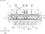
- FIG. 15 is a sectional view taken along line XV-XV in FIG. 3.
- FIG. 16 is an enlarged perspective view of a holder that constitutes a control terminal.
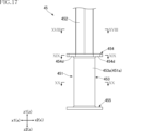
- FIG. 17 is a partially enlarged front view of the control terminal.
- FIG. 18 is a cross-sectional view taken along line XVIII-XVIII in FIG. 17.
- FIG. 19 is a sectional view taken along line XIX-XIX in FIG. 17.
- FIG. 20 is a sectional view taken along line XX-XX in FIG. 17.
- FIG. 21 is a plan view similar to FIG. 4, showing a semiconductor device according to a first modification of the first embodiment.
- FIG. 22 is a partially enlarged front view of a control terminal in a semiconductor device according to a first modification of the first embodiment.
- FIG. 23 is a cross-sectional view taken along line XXIII-XXIII in FIG. 22.
- FIG. 24 is a sectional view taken along line XXIV-XXIV in FIG. 22.
- FIG. 25 is a cross-sectional view taken along line XXV-XXV in FIG. 22.
- FIG. 26 is a partially enlarged front view showing another modification of the control terminal.
- FIG. 27 is a cross-sectional view taken along line XXVII-XXVII in FIG. 26.
- FIG. 28 is a cross-sectional view taken along line XXVIII-XXVIII in FIG. 26.
- FIG. 29 is a cross-sectional view taken along line XXIX-XXIX in FIG. 26.
- FIG. 30 is a sectional view taken along the line XXX-XXX in FIG. 26.
- a thing A is formed on a thing B and "a thing A is formed on a thing B” mean “a thing A is formed on a thing B” unless otherwise specified.
- "something A is placed on something B” and “something A is placed on something B” mean "something A is placed on something B” unless otherwise specified.
- a certain surface A faces (one side or the other side of) the direction B is not limited to the case where the angle of the surface A with respect to the direction B is 90 degrees; Including cases where it is tilted to the opposite direction.
- First embodiment: 1 to 20 show a semiconductor device according to a first embodiment of the present disclosure.
- the semiconductor device A1 of this embodiment includes a plurality of first semiconductor elements 10A, a plurality of second semiconductor elements 10B, a support substrate 3, a first main terminal 41, a second main terminal 42, a third main terminal 43, a plurality of control It includes a terminal 45 and a plurality of wires 51, 52, 53, 54, 551, 552, 561, 562.
- the semiconductor device A1 further includes a case 6, a heat sink 7, a sealing part 81, and a lid 82.
- FIG. 1 is a perspective view showing a semiconductor device A1.
- FIG. 2 is a plan view showing the semiconductor device A1.
- FIG. 3 is a plan view showing the semiconductor device A1, and for convenience of understanding, the lid 82 and the sealing part 81 are omitted.
- FIG. 4 is a plan view showing the semiconductor device A1, with the case 6 omitted from the plan view of FIG.
- FIG. 5 is an enlarged view in which the heat sink 7, the first main terminal 41, the second main terminal 42, and the third main terminal 43 are omitted from the plan view of FIG.
- FIG. 6 is a front view showing the semiconductor device A1.
- FIG. 7 is a rear view of the semiconductor device A1.
- FIG. 8 is a right side view showing the semiconductor device A1.
- FIG. 1 is a perspective view showing a semiconductor device A1.
- FIG. 2 is a plan view showing the semiconductor device A1.
- FIG. 3 is a plan view showing the semiconductor device A1, and for convenience of understanding, the lid 82 and the sealing
- FIG. 9 is a left side view showing the semiconductor device A1.
- FIG. 10 is a bottom view showing the semiconductor device A1.
- FIG. 11 is a cross-sectional view taken along line XI-XI in FIG. 3.
- FIG. 12 is a sectional view taken along line XII-XII in FIG. 3.
- FIG. 13 is a cross-sectional view taken along line XIII-XIII in FIG.
- FIG. 14 is a cross-sectional view taken along line XIV-XIV in FIG. 3.
- FIG. 15 is a sectional view taken along line XV-XV in FIG. 3.
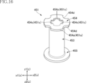
- FIG. 16 is an enlarged perspective view of the holder 451 that constitutes the control terminal 45. As shown in FIG. FIG. 17 is a partially enlarged front view of the control terminal.
- FIG. 17 is a partially enlarged front view of the control terminal.
- FIG. 18 is a cross-sectional view taken along line XVIII-XVIII in FIG. 17.
- FIG. 19 is a sectional view taken along line XIX-XIX in FIG. 17.
- FIG. 20 is a sectional view taken along line XX-XX in FIG. 17.
- the thickness direction of the support substrate 3 will be referred to as the "thickness direction z.”
- One direction perpendicular to the thickness direction z is referred to as a “first direction x.”
- a direction perpendicular to both the thickness direction z and the first direction x is referred to as a "second direction y.”
- the plurality of first semiconductor elements 10A and the plurality of second semiconductor elements 10B are each electronic components that serve as the functional center of the semiconductor device A1.
- the constituent material of each first semiconductor element 10A and each second semiconductor element 10B is, for example, a semiconductor material mainly composed of SiC (silicon carbide). This semiconductor material is not limited to SiC, and may be Si (silicon), GaN (gallium nitride), C (diamond), or the like.
- Each of the first semiconductor elements 10A and each of the second semiconductor elements 10B is a power semiconductor chip having a switching function, such as a MOSFET (Metal Oxide Semiconductor Field Effect Transistor).
- MOSFET Metal Oxide Semiconductor Field Effect Transistor
- first semiconductor element 10A and the second semiconductor element 10B are MOSFETs, but the present invention is not limited to this, and other transistors such as IGBTs (Insulated Gate Bipolar Transistors) can be used. There may be.
- Each first semiconductor element 10A and each second semiconductor element 10B are the same element.
- Each first semiconductor element 10A and each second semiconductor element 10B is, for example, an n-channel MOSFET, but may be a p-channel MOSFET.
- the first semiconductor element 10A and the second semiconductor element 10B each have an element main surface 101 and an element rear surface 102, as shown in FIGS. 11 to 13.
- the element main surface 101 and the element back surface 102 are separated in the thickness direction z.
- the element main surface 101 faces the z1 side in the thickness direction z
- the element back surface 102 faces the z2 side in the thickness direction z.
- the semiconductor device A1 includes six first semiconductor elements 10A and six second semiconductor elements 10B, but the number of first semiconductor elements 10A and the number of second semiconductor elements 10B are , is not limited to this configuration, and may be changed as appropriate depending on the performance required of the semiconductor device A1.
- six first semiconductor elements 10A and six second semiconductor elements 10B are arranged.
- the number of the first semiconductor elements 10A and the second semiconductor elements 10B may be four or five, or seven or more each.
- the number of first semiconductor elements 10A and the number of second semiconductor elements 10B may be equal or different.
- the number of first semiconductor elements 10A and second semiconductor elements 10B is determined by the current capacity handled by semiconductor device A1.
- the semiconductor device A1 is configured, for example, as a half-bridge switching circuit.
- the plurality of first semiconductor elements 10A constitute an upper arm circuit of the semiconductor device A1
- the plurality of second semiconductor elements 10B constitute a lower arm circuit.
- the plurality of first semiconductor elements 10A are connected to each other in parallel
- the first semiconductor elements 10A are connected to each other in parallel
- the plurality of second semiconductor elements 10B are connected to each other in parallel. connected in parallel.
- Each first semiconductor element 10A and each second semiconductor element 10B are connected in series and constitute a bridge layer.
- the plurality of first semiconductor elements 10A are each mounted on a first conductive portion 32A of the support substrate 3, which will be described later, as shown in FIGS. 3 to 5, FIG. 11, and the like. Each first semiconductor element 10A is conductively bonded to the first conductive portion 32A via a conductive bonding material 19. When each first semiconductor element 10A is joined to the first conductive part 32A, the element back surface 102 faces the first conductive part 32A.
- the plurality of first semiconductor elements 10A may be mounted on a metal member different from a part of the DBC substrate or the like. In this case, the metal member corresponds to the first conductive part in the present disclosure. This metal member may be supported by, for example, a DBC board or the like.
- the plurality of second semiconductor elements 10B are each mounted on a second conductive portion 32B of the support substrate 3, which will be described later, as shown in FIGS. 3 to 5, FIG. 11, and FIG. 12.
- Each second semiconductor element 10B is conductively bonded to a second conductive portion 32B via a conductive bonding material 19.
- the element back surface 102 faces the second conductive part 32B.
- the plurality of second semiconductor elements 10B may be mounted on a metal member different from a part of the DBC substrate or the like.
- the metal member corresponds to the second conductive part in the present disclosure. This metal member may be supported by, for example, a DBC board or the like.
- the plurality of first semiconductor elements 10A and the plurality of second semiconductor elements 10B each have a first main surface electrode 11, a second main surface electrode 12, a third main surface electrode 13, and a back electrode 15.
- the configurations of the first main surface electrode 11, second main surface electrode 12, third main surface electrode 13, and back surface electrode 15 described below are common to each first semiconductor element 10A and each second semiconductor element 10B.
- the first main surface electrode 11, the second main surface electrode 12, and the third main surface electrode 13 are provided on the element main surface 101.
- the first main surface electrode 11, the second main surface electrode 12, and the third main surface electrode 13 are insulated by an insulating film (not shown).
- the back electrode 15 is provided on the back surface 102 of the element.
- the first principal surface electrode 11 is, for example, a gate electrode, and a drive signal (for example, gate voltage) for driving the first semiconductor element 10A (second semiconductor element 10B) is input.
- the second main surface electrode 12 is, for example, a source electrode, through which a source current flows.
- the third main surface electrode 13 is, for example, a source sense electrode, through which a source current flows.
- the third main surface electrode 13 of the present embodiment is composed of two separate regions when viewed in the thickness direction z.
- the back electrode 15 is, for example, a drain electrode, through which a drain current flows.
- the back electrode 15 covers the entire area (or substantially the entire area) of the back surface 102 of the element.
- the back electrode 15 is made of, for example, Ag (silver) plating.
- each first semiconductor element 10A (each second semiconductor element 10B) changes between a conductive state and a disconnected state according to this drive signal. The state changes. In a conductive state, a current flows from the back electrode 15 (drain electrode) to the second main surface electrode 12 (source electrode), and in a cutoff state, this current does not flow. That is, each first semiconductor element 10A (each second semiconductor element 10B) performs a switching operation.
- the semiconductor device A1 converts the DC voltage input between the first main terminal 41 and the second main terminal 42 into, for example, an AC voltage by the switching function of the plurality of first semiconductor elements 10A and the plurality of second semiconductor elements 10B. After conversion, an AC voltage is output from the third main terminal 43.
- Each of the plurality of first semiconductor elements 10A and the plurality of second semiconductor elements 10B described above is an example of a "semiconductor element".
- the semiconductor device A1 includes a thermistor 17, as shown in FIGS. 3 to 5.
- the thermistor 17 is used as a temperature detection sensor. Note that, in addition to the thermistor 17, the configuration may include, for example, a temperature-sensitive diode, or the configuration may not include the thermistor 17 or the like.
- the support substrate 3 supports the plurality of first semiconductor elements 10A and the plurality of second semiconductor elements 10B.
- the specific structure of the support substrate 3 is not limited at all, and may be formed of, for example, a DBC (Direct Bonded Copper) substrate or an AMB (Active Metal Brazing) substrate.
- Support substrate 3 includes an insulating substrate 31, a support conductor 32, and a back metal layer 33.
- the dimension of the support substrate 3 in the z direction is, for example, 0.4 mm or more and 3.0 mm or less.
- the insulating substrate 31 is made of, for example, ceramics with excellent thermal conductivity. Such ceramics include, for example, SiN (silicon nitride).
- the insulating substrate 31 is not limited to ceramics, and may be an insulating resin sheet or the like.
- the insulating substrate 31 has, for example, a rectangular shape in plan view.
- the dimension of the insulating substrate 31 in the thickness direction z is not particularly limited, and is, for example, 0.05 mm or more and 1.0 mm or less.
- the support conductor 32 includes a first conductive portion 32A, a second conductive portion 32B, and a third conductive portion 32C.
- the support conductor 32 further includes a first gate section 326A, a second gate section 326B, a first detection section 327A, a second detection section 327B, and a thermistor mounting section 328.
- Each part of the support conductor 32 is laminated on the upper surface of the insulating substrate 31 (the surface facing the z1 side in the thickness direction z). As shown in FIGS.
- each part of the support conductor 32 (first conductive part 32A, second conductive part 32B, third conductive part 32C, first gate part 326A, second gate part 326B, first detection part 327A, second detection section 327B, and thermistor mounting section 328) have a main surface 320.
- the main surface 320 is a plane facing the z1 side in the thickness direction z.
- the constituent material of the support conductor 32 includes, for example, Cu (copper).
- the constituent material may include, for example, Al (aluminum) other than Cu (copper).
- the dimension of the support conductor 32 in the thickness direction z is not particularly limited, and is, for example, 0.1 mm or more and 1.5 mm or less.
- the first conductive part 32A supports the plurality of first semiconductor elements 10A. As shown in FIG. 11, a plurality of first semiconductor elements 10A are each bonded to the main surface 320 of the first conductive portion 32A via a conductive bonding material 19.
- the constituent material of the conductive bonding material 19 is not particularly limited, and may be, for example, solder, metal paste material, or sintered metal.
- the first conductive part 32A has a first wiring part 321, a second wiring part 322, and a first communication part 325A, as shown in FIGS. 4 and 5.
- the first wiring section 321 and the second wiring section 322 are spaced apart from each other on the x1 side of the first direction x and the x2 side of the first direction x, and each extends in the second direction y.
- the first wiring section 321 is located on the insulating substrate 31 at the end on the x1 side in the first direction x
- the second wiring section 322 is located on the insulating substrate 31 at the end on the x2 side in the first direction x. Located at the edge.
- a plurality of first semiconductor elements 10A are arranged in each of the first wiring section 321 and the second wiring section 322.
- three first semiconductor elements 10A are arranged in each of the first wiring part 321 and the second wiring part 322.
- the three first semiconductor elements 10A arranged in the first wiring section 321 are arranged at intervals along the second direction y.
- the interval between the first semiconductor elements 10A adjacent to each other in the second direction y on the first wiring portion 321 is greater than the length of the first semiconductor elements 10A in the second direction y.
- the three first semiconductor elements 10A arranged in the second wiring section 322 are similarly arranged at intervals along the second direction y.
- the interval between the first semiconductor elements 10A adjacent to each other in the second direction y on the second wiring portion 322 is greater than the length of the first semiconductor elements 10A in the second direction y.
- the first wiring section 321 has a first end 321a.
- the first end portion 321a is located on the y2 side in the second direction y in the first wiring portion 321.
- the second wiring section 322 has a second end 322a.
- the second end portion 322a is located on the y2 side of the second wiring portion 322 in the second direction y.
- the first communication portion 325A is connected to both the first end 321a and the second end 322a.
- the first communication portion 325A is located on the insulating substrate 31 closer to the y2 side in the second direction y. In the illustrated example, the first communication portion 325A is approximately U-shaped.
- the second conductive part 32B supports the plurality of second semiconductor elements 10B. As shown in FIGS. 12 and 13, a plurality of second semiconductor elements 10B are each bonded to the main surface 320 of the second conductive portion 32B via a conductive bonding material 19.
- the conductive bonding material 19 for bonding the plurality of first semiconductor elements 10A and the plurality of second semiconductor elements 10B to the main surface 320 is an example of a "second conductive bonding material.”
- the second conductive part 32B has a third wiring part 323, a fourth wiring part 324, and a second communication part 325B, as shown in FIGS. 4 and 5.
- the third wiring section 323 and the fourth wiring section 324 are spaced apart from each other on the x1 side in the first direction x and on the x2 side in the first direction x, and each extends in the second direction y.
- the third wiring section 323 and the fourth wiring section 324 are arranged between the first wiring section 321 and the second wiring section 322 in the first direction x.
- a plurality of second semiconductor elements 10B are arranged in each of the third wiring section 323 and the fourth wiring section 324.
- three second semiconductor elements 10B are arranged in each of the third wiring part 323 and the second wiring part 322.
- the three second semiconductor elements 10B arranged in the third wiring section 323 are arranged at intervals along the second direction y.
- the interval between adjacent second semiconductor elements 10B in the second direction y on the third wiring section 323 is greater than the length of the second semiconductor elements 10B in the second direction y.
- the three second semiconductor elements 10B arranged in the fourth wiring section 324 are similarly arranged at intervals along the second direction y.
- the interval between adjacent second semiconductor elements 10B in the second direction y on the fourth wiring section 324 is greater than the length of the second semiconductor elements 10B in the second direction y.
- the third wiring section 323 has a third end 323a.
- the third end portion 323a is located on the y2 side in the second direction y in the third wiring portion 323.
- the fourth wiring section 324 has a fourth end 324a.
- the fourth end portion 324a is located on the y2 side in the second direction y in the fourth wiring portion 324.
- the second communication portion 325B is connected to both the third end 323a and the fourth end 324a.
- the second communication portion 325B is located on the insulating substrate 31 closer to the y2 side in the second direction y.
- the plurality (three) of first semiconductor elements 10A arranged in the first wiring part 321 and the plurality (three) of second semiconductor elements 10B arranged in the third wiring part 323 are as follows. They are arranged alternately in the second direction y.
- "disposed alternately” means that the plurality of first semiconductor elements 10A on the first wiring part 321 and the plurality of second semiconductor elements 10B on the third wiring part 323 are arranged in the second direction y. It means an aspect in which the positions are not aligned intentionally but are shifted, and the same applies to the following description.
- the first semiconductor element 10A on the first wiring part 321 and the second semiconductor element 10B on the third wiring part 323 may partially overlap when viewed in the first direction x.
- one first semiconductor element 10A and one second semiconductor element 10B partially overlap when viewed in the first direction x.
- a plurality of (three) first semiconductor elements 10A arranged in the second wiring part 322 and a plurality (three) of second semiconductor elements 10B arranged in the fourth wiring part 324 are arranged in the second direction y. are arranged alternately.
- the first semiconductor element 10A on the second wiring part 322 and the second semiconductor element 10B on the fourth wiring part 324 may partially overlap when viewed in the first direction x.
- the plurality of first semiconductor elements 10A arranged in the second wiring part 322 and the plurality of second semiconductor elements 10B arranged in the fourth wiring part 324 overlap when viewed in the first direction x. No.
- the semiconductor device A1 also includes a plurality (three) of first semiconductor elements 10A arranged in the first wiring part 321 and a plurality (three) of first semiconductor elements 10A arranged in the second wiring part 322. are arranged alternately in the second direction y.
- the first semiconductor element 10A on the first wiring part 321 and the first semiconductor element 10A on the second wiring part 322 may partially overlap when viewed in the first direction x.
- one of the plurality of first semiconductor elements 10A arranged in the first wiring part 321 and the plurality of first semiconductor elements 10A arranged in the second wiring part 322 is one on the first wiring part 321.
- the two first semiconductor elements 10A and the one first semiconductor element 10A on the second wiring section 322 partially overlap when viewed in the first direction x.
- the third conductive portion 32C is disposed between the third wiring portion 323 and the fourth wiring portion 324 in the first direction x.
- the third conductive portion 32C extends in the second direction y.
- the first conductive part 32A, the second conductive part 32B, and the third conductive part 32C are switched by the plurality of first semiconductor elements 10A and the plurality of second semiconductor elements 10B together with the plurality of wires 51, 52, 53, and 54. Configure the main circuit current path.
- the first gate portion 326A is electrically connected to the first main surface electrode 11 of the plurality of first semiconductor elements 10A.
- the first gate portion 326A is arranged in a plurality of regions.
- the first gate section 326A is located between the first interconnect section 321 and the third interconnect section 323, between the second interconnect section 322 and the fourth interconnect section 324, and between the third conductive section 32C and the third interconnect section 323. 2 communication portion 325B.
- the first detection section 327A is electrically connected to the third main surface electrode 13 of the plurality of first semiconductor elements 10A.
- the first detection units 327A are arranged in multiple areas. In the illustrated example, the first detection section 327A is located between the first wiring section 321 and the third wiring section 323, between the second wiring section 322 and the fourth wiring section 324, and between the third conductive section 32C and the third wiring section 323. 2 communication portion 325B.
- the second gate portion 326B is electrically connected to the first main surface electrodes 11 of the plurality of second semiconductor elements 10B.
- the second gate section 326B is arranged between the third conductive section 32C and the fourth wiring section 324, and extends in the second direction y.
- the second detection section 327B is electrically connected to the third main surface electrodes 13 of the plurality of second semiconductor elements 10B.
- the second detection section 327B is arranged between the third conductive section 32C and the fourth wiring section 324, and extends in the second direction y.
- the thermistor mounting portions 328 are provided in pairs, as shown in FIG.
- the pair of thermistor mounting portions 328 are spaced apart from each other in the second direction y, and have the thermistor 17 mounted thereon.
- the pair of thermistor mounting parts 328 are located near the corners of the insulating substrate 31.
- the back metal layer 33 is formed on the lower surface of the insulating substrate 31 (the surface facing the z2 side in the thickness direction z).
- the constituent material of the back metal layer 33 is the same as that of the supporting conductor 32.
- Back metal layer 33 has a bottom surface 332 .
- the bottom surface 332 is a plane facing toward the z2 side in the thickness direction z.
- a heat sink 7, which will be described later, is attached to the bottom surface 332.
- the first main terminal 41, the second main terminal 42, and the third main terminal 43 are external connection terminals provided in the semiconductor device A1, as shown in FIGS. 1 to 4 and the like.
- the first main terminal 41, the second main terminal 42, and the third main terminal 43 are each made of a plate-shaped metal plate.
- This metal plate includes, for example, Cu (copper) or a Cu (copper) alloy.
- the thickness of the metal plate is not particularly limited, and is, for example, about 1.0 mm.
- the first main terminal 41 and the second main terminal 42 are connected to a DC power supply placed outside the semiconductor device A1.
- a DC voltage to be subjected to power conversion is input to the first main terminal 41 and the second main terminal 42 .
- the first main terminal 41 is a positive electrode (P terminal)
- the second main terminal 42 is a negative electrode (N terminal).
- the first main terminal 41 and the second main terminal 42 are arranged on the y1 side in the second direction y with respect to the support conductor 32 (the first conductive part 32A and the second conductive part 32B).
- the first main terminal 41 and the second main terminal 42 are supported by the case 6.
- the first main terminal 41 has an external connection part 411, an internal connection part 412, and an intermediate part 413.
- the external connection portion 411 is exposed from the semiconductor device A1 and has a flat plate shape orthogonal to the thickness direction z.
- a DC power cable or the like is connected to the external connection part 411.
- External connection part 411 is supported by case 6.
- the external connection portion 411 is provided with a connection hole 411a penetrating in the thickness direction z.
- a fastening member such as a bolt is inserted into the connection hole 411a.
- a nut 419 is fixed to the z2 side of the external connection portion 411 in the thickness direction z.
- the nut 419 is arranged corresponding to the connection hole 411a, and a fastening member such as a bolt inserted into the connection hole 411a fits into the nut 419.
- a fastening member such as a bolt inserted into the connection hole 411a fits into the nut 419.
- the surface of the external connection portion 411 may be plated with nickel (Ni).
- the internal connection part 412 is electrically connected to the first conductive part 32A.
- the internal connection portion 412 has a comb-teeth shape that is electrically connected to the first wiring portion 321 and the second wiring portion 322 of the first conductive portion 32A.
- internal connection portion 412 has four teeth. The plurality of teeth are bent in the thickness direction z. Therefore, the plurality of teeth are hook-shaped when viewed in the first direction x. Two teeth of the internal connection part 412 are electrically connected to the end of the first wiring part 321 on the y1 side in the second direction y, and the other two teeth of the internal connection part 412 are connected to the end of the first wiring part 321 on the y1 side in the second direction y.
- the intermediate portion 413 interconnects the external connection portion 411 and the internal connection portion 412.
- the intermediate portion 413 has an L-shaped cross section in the first direction x.
- the first main terminal 41 is electrically connected to the first conductive part 32A and, via the first conductive part 32A, to the back electrode 15 (drain electrode) of each first semiconductor element 10A.
- the second main terminal 42 has an external connection part 421, an internal connection part 422, and an intermediate part 423.
- the external connection portion 421 is exposed from the semiconductor device A1 and has a flat plate shape orthogonal to the thickness direction z.
- a DC power cable or the like is connected to the external connection part 421.
- the external connection section 421 is supported by the case 6.
- the external connection part 421 is arranged on the x1 side in the first direction x with respect to the external connection part 411 of the first main terminal 41.
- the external connection portion 421 is provided with a connection hole 421a that penetrates in the thickness direction z.
- a fastening member such as a bolt is inserted into the external connection portion 421 .
- a nut 429 is fixed to the z2 side of the external connection portion 421 in the thickness direction z.
- the nut 429 is arranged corresponding to the connection hole 421a, and a fastening member such as a bolt inserted into the connection hole 421a fits into the nut 429.
- a fastening member such as a bolt inserted into the connection hole 421a fits into the nut 429.
- the surface of the external connection portion 421 may be plated with nickel.
- the internal connection part 422 is electrically connected to the third conductive part 32C.
- the internal connection portion 422 has a comb-teeth shape that is electrically connected to the third conductive portion 32C.
- the internal connection portion 422 has four teeth, and these teeth are arranged along the first direction x.
- the plurality of teeth are bent in the thickness direction z. Therefore, the plurality of teeth are hook-shaped when viewed in the first direction x.
- the plurality of teeth of the internal connection part 412 are electrically connected to the end of the third conductive part 32C on the y1 side in the second direction y.
- the method of conductive bonding is not limited at all, and methods such as ultrasonic bonding, laser bonding, welding, or methods using solder, metal paste, silver sintered body, etc. are appropriately employed.
- the intermediate portion 423 interconnects the external connection portion 421 and the internal connection portion 422.
- the intermediate portion 423 has an L-shaped cross section in the first direction x.
- the third conductive portion 32C and the second main surface electrode 12 of each second semiconductor element 10B are electrically connected via wires 53, which will be described later.
- the second main terminal 42 is electrically connected to the third conductive portion 32C and, via the third conductive portion 32C, to the second main surface electrode 12 (source electrode) of each second semiconductor element 10B.
- the third main terminal 43 is connected to a power supply target placed outside the semiconductor device A1.
- the third main terminal 43 outputs an AC voltage whose power has been converted by the first semiconductor element 10A and the second semiconductor element 10B.
- the third main terminal 43 is arranged on the y2 side in the second direction y with respect to the support conductor 32 (the first conductive part 32A and the second conductive part 32B).
- the third main terminal 43 is supported by the case 6.
- the third main terminal 43 has an external connection part 431, an internal connection part 432, and an intermediate part 433.
- the external connection portion 431 is exposed from the semiconductor device A1 and has a flat plate shape orthogonal to the thickness direction z.
- a cable or the like that is electrically connected to the power supply target is connected to the external connection section 431 .
- the external connection portion 431 is provided with a connection hole 431a penetrating in the thickness direction z.
- a fastening member such as a bolt is inserted into the connection hole 411a.
- the surface of the external connection portion 431 may be plated with nickel.
- the internal connection part 432 is electrically connected to the second conductive part 32B.
- the internal connection portion 432 has a comb-teeth shape that is electrically connected to the second communication portion 325B of the second conductive portion 32B.
- the internal connection portion 432 has four teeth, and these teeth are arranged along the first direction x.
- the plurality of teeth are bent in the thickness direction z. Therefore, the plurality of teeth are hook-shaped when viewed in the first direction x.
- the plurality of teeth of the internal connection part 432 are electrically connected to the second communication part 325B of the second conductive part 32B.
- the method of conductive bonding is not limited at all, and methods such as ultrasonic bonding, laser bonding, welding, or methods using solder, metal paste, silver sintered body, etc. are appropriately employed.
- the intermediate portion 433 interconnects the external connection portion 431 and the internal connection portion 432.
- the intermediate portion 433 is connected to the external connection portion 431 and extends continuously, and has a flat plate shape orthogonal to the thickness direction z.
- the intermediate portion 433 is supported by the case 6.
- the third main terminal 43 is electrically connected to the second conductive portion 32B and, via the second conductive portion 32B, to the back electrode 15 (drain electrode) of each second semiconductor element 10B.
- Each of the plurality of control terminals 45 is a pin-shaped terminal for controlling the driving of each first semiconductor element 10A and each second semiconductor element 10B.
- Each of the plurality of control terminals 45 is, for example, a press-fit terminal.
- Each of the plurality of control terminals 45 is arranged on the main surface 320 of the support conductor 32 and extends toward the z1 side in the thickness direction z.
- the plurality of control terminals 45 include a plurality of first control terminals 46A-46E and a plurality of second control terminals 47A-47C.
- the plurality of first control terminals 46A to 46E are used for controlling each first semiconductor element 10A.
- the plurality of second control terminals 47A to 47C are used for controlling each second semiconductor element 10B.
- the plurality of first control terminals 46A to 46E are supported by the support substrate 3 (support conductor 32).
- the plurality of first control terminals 46A to 46E are arranged on the support substrate 3 closer to the y2 side in the second direction y.
- the first control terminal 46A is a terminal (gate terminal) for inputting a drive signal for the plurality of first semiconductor elements 10A.
- a drive signal for driving the plurality of first semiconductor elements 10A is input to the first control terminal 46A (for example, a gate voltage is applied).
- the first control terminal 46A is supported by the first gate portion 326A.
- the first control terminal 46B is a source signal detection terminal (source sense terminal) of the plurality of first semiconductor elements 10A.
- the voltage (voltage corresponding to the source current) applied to each second main surface electrode 12 (source electrode) of the plurality of first semiconductor elements 10A is detected from the first control terminal 46B.
- the first control terminal 46B is supported by the first detection section 327A.
- the first control terminal 46C is a drain signal detection terminal (drain sense terminal) of the plurality of first semiconductor elements 10A.
- the voltage (voltage corresponding to the drain current) applied to each back electrode 15 (drain electrode) of the plurality of first semiconductor elements 10A is detected from the first control terminal 46C.
- the first control terminal 46C is supported by the first conductive portion 32A (first end portion 321a of the first wiring portion 321).
- the first control terminal 46D and the first control terminal 46E are terminals that are electrically connected to the thermistor 17.
- the first control terminal 46D and the first control terminal 46E are each supported by the thermistor mounting portion 328.
- the plurality of second control terminals 47A to 47C are supported by the support substrate 3 (support conductor 32).
- the plurality of second control terminals 47A to 47C are arranged on the support substrate 3 closer to the y1 side in the second direction y.
- the second control terminal 47A is a terminal (gate terminal) for inputting drive signals for the plurality of second semiconductor elements 10B.
- a drive signal for driving the plurality of second semiconductor elements 10B is input to the second control terminal 47A (for example, a gate voltage is applied).
- the second control terminal 47A is supported by the second gate portion 326B.
- the second control terminal 47B is a source signal detection terminal (source sense terminal) of the plurality of second semiconductor elements 10B.
- the voltage (voltage corresponding to the source current) applied to each second main surface electrode 12 (source electrode) of the plurality of second semiconductor elements 10B is detected from the second control terminal 47B.
- the second control terminal 47B is supported by the second detection section 327B.
- the second control terminal 47C is a drain signal detection terminal (drain sense terminal) of the plurality of second semiconductor elements 10B.
- the voltage (voltage corresponding to the drain current) applied to each back electrode 15 (drain electrode) of the plurality of second semiconductor elements 10B is detected from the second control terminal 47C.
- the second control terminal 47C is supported by the second conductive portion 32B (fourth wiring portion 324).
- Each of the plurality of control terminals 45 (the plurality of first control terminals 46A to 46E and the plurality of second control terminals 47A to 47C) includes a holder 451 and a metal pin 452.
- the holder 451 is made of a conductive material. As shown in FIGS. 14 and 15, the holder 451 attaches each part of the supporting conductor 32 (the above-described first gate part 326A, first detection part 327A, first conductive part 32A, etc.) via a conductive bonding material 459. is joined to the main surface 320 of.
- the conductive bonding material 459 for bonding the holder 451 to the main surface 320 is an example of a "first conductive bonding material.”
- Holder 451 has an outer circumferential surface 451a and an inner circumferential surface 451b.
- the outer circumferential surface 451a is a surface facing outward in the radial direction of the holder 451 when viewed in the thickness direction z.
- the inner circumferential surface 451b faces opposite to the outer circumferential surface 451a, and is a surface facing inward in the radial direction of the holder 451 when viewed in the thickness direction z.
- the outer circumferential surface 451a includes a first outer circumferential surface 454a belonging to the first collar portion 454 and a second outer circumferential surface 453a belonging to the cylindrical portion 453.
- the inner circumferential surface 451b includes a first inner circumferential surface 454b belonging to the first collar portion 454 and a second inner circumferential surface 453b belonging to the cylindrical portion 453.
- the cylindrical portion 453 extends in the thickness direction z and has a cylindrical shape, for example.
- the cylindrical portion 453 has a second outer circumferential surface 453a and a second inner circumferential surface 453b.
- the first flange portion 454 is connected to the end portion of the cylindrical portion 453 on the z1 side in the thickness direction z.
- the first flange portion 454 extends radially outward from the cylindrical portion 453 when viewed in the thickness direction z.
- the first flange portion 454 has an annular shape when viewed in the thickness direction z.
- the first flange portion 454 has a first outer circumferential surface 454a and a first inner circumferential surface 454b.
- the second flange portion 455 is connected to the end of the cylindrical portion 453 on the z2 side in the thickness direction z.
- the second flange portion 455 extends radially outward from the cylindrical portion 453 when viewed in the thickness direction z.
- the second flange portion 455 is bonded to the main surface 320 (support conductor 32) via a conductive bonding material 459.
- a plurality of convex portions 451c are provided on the inner peripheral surface 451b of the holder 451.
- the convex portion 451c protrudes radially inward from the inner circumferential surface 451b.
- the plurality of convex portions 451c include a plurality of first convex portions 454c.
- the first convex portion 454c is provided on the first inner circumferential surface 454b of the first collar portion 454 among the convex portions 451c.
- a plurality (four) of first convex portions 454c are provided on the inner circumferential surface 451b of the holder 451 (the first inner circumferential surface 454b of the first collar portion 454).
- the plurality (four) of first convex portions 454c include two first convex portions 454c that face each other across the axis of the holder 451.
- two sets of two first convex portions 454c are provided that face each other across the axis of the holder 451, and one set and the other set are positioned at different positions in the circumferential direction around the axis of the holder 451. It's 90 degrees off.
- the method of forming the plurality of first convex portions 454c is not particularly limited, and may be formed by embossing, for example.
- a plurality (four) of first recesses 454d are formed in the first outer circumferential surface 454a of the first flange 454.
- the plurality of first concave portions 454d correspond to the plurality of first convex portions 454c, respectively, and are traces when the plurality of first convex portions 454c were formed.
- the metal pin 452 is a rod-shaped member extending in the thickness direction z.
- the cross-sectional shape of the metal pin 452 perpendicular to the thickness direction z is a rectangular shape.
- the metal pin 452 is supported by being press-fitted into the holder 451.
- a metal pin 452 is inserted through at least the first collar portion 454 and the cylindrical portion 453 of the holder 451 .
- the metal pin 452 is electrically connected to the support conductor 32 via the holder 451 and the conductive bonding material 459.
- the metal pin 452 when the metal pin 452 is press-fitted into the holder 451, the inner circumferential surface 451b of the holder 451 and the outer circumferential surface 452a of the metal pin 452 are in appropriate contact.
- the metal pin 452 has its four corners connected to a plurality of (four) first convex portions 454c provided on the first inner circumferential surface 454b of the first flange portion 454. It is press-fitted into the holder 451 with the orientation shifted by 45 degrees.
- the plurality of first convex portions 454c provided on the first inner circumferential surface 454b of the first collar portion 454 are in contact with the outer circumferential surface 452a of the metal pin 452.
- a pin recess 452d is formed on the outer circumferential surface 452a of the metal pin 452 at a portion where the first protrusion 454c comes into contact.
- the original cross-sectional shape of the metal pin 452 is represented by a dotted line.
- the four corners of the metal pin 452 are shown crushed inward in the radial direction with respect to the inner peripheral surface 451b, but the four corners of the metal pin 452
- the inner circumferential surface 451b may be expanded outward in the radial direction.
- the four corners of the metal pin 452 may be crushed radially inward with respect to the inner circumferential surface 451b, and the inner circumferential surface 451b may be pushed outward in the radial direction by the four corners of the metal pin 452. .
- the plurality of first protrusions 454c are formed by embossing as described above
- the pressing member By pressing, the first protrusion 454c and the first recess 454d are formed.
- the plurality of wires 51, 52, 53, 54 shown in FIG. 4 and FIG. 2 constitutes a path for the main circuit current switched by the semiconductor element 10B.
- the plurality of wires 51 are conductive members that connect the plurality of first semiconductor elements 10A and the third wiring section 323. Each of the plurality of wires 51 is connected to the second main surface electrode 12 (source electrode) of the first semiconductor element 10A arranged on the first wiring part 321 and the third wiring part 323, and is connected to the third wiring part 323. The second principal surface electrode 12 and the third wiring portion 323 are electrically connected. In the illustrated example, a plurality of (four) wires 51 are connected to one first semiconductor element 10A. Each wire 51 has a first part 511 and a second part 512.
- the first portion 511 is a bonded end portion bonded to the second main surface electrode 12 of the first semiconductor element 10A.
- the second portion 512 is a joint end portion joined to the third wiring portion 323.
- at least one of the second portions 512 of the plurality of wires 51 is arranged between the second semiconductor elements 10B adjacent to each other in the second direction y on the third wiring portion 323.
- the wire 51 is made of aluminum (Al) or copper (Cu), for example. Note that the constituent material, wire diameter, and number of wires 51 are not limited.
- the wire 51 is a conductive member connected to the second main surface electrode 12 (source electrode) of the first semiconductor element 10A and the third wiring section 323; Instead, it may be constructed from a metal plate.
- the plurality of wires 52 are conductive members that connect the plurality of first semiconductor elements 10A and the fourth wiring section 324. Each of the plurality of wires 52 is connected to the second main surface electrode 12 (source electrode) of the first semiconductor element 10A arranged on the second wiring part 322 and the fourth wiring part 324, and is connected to the fourth wiring part 324. The second principal surface electrode 12 and the fourth wiring portion 324 are electrically connected. In the illustrated example, a plurality of (four) wires 52 are connected to one first semiconductor element 10A. Each wire 52 has a third portion 521 and a fourth portion 522.
- the third portion 521 is a bonded end portion bonded to the second main surface electrode 12 of the first semiconductor element 10A.
- the fourth portion 522 is a joint end portion joined to the fourth wiring portion 324.
- at least one of the fourth portions 522 of the plurality of wires 52 is arranged between the second semiconductor elements 10B adjacent to each other in the second direction y on the fourth wiring portion 324.
- the wire 52 is made of aluminum (Al) or copper (Cu), for example. Note that the constituent material, wire diameter, and number of wires 52 are not limited.
- the wire 52 is a conductive member connected to the second main surface electrode 12 (source electrode) of the first semiconductor element 10A and the fourth wiring section 324; Instead, it may be constructed from a metal plate.
- the plurality of wires 53 are conductive members that connect the plurality of second semiconductor elements 10B and the third conductive portion 32C. Each of the plurality of wires 53 is connected to the second main surface electrode 12 (source electrode) of the second semiconductor element 10B arranged on the third wiring part 323 and the third conductive part 32C, and is connected to the third conductive part 32C. The second principal surface electrode 12 and the third conductive portion 32C are electrically connected. In the illustrated example, a plurality of (four) wires 53 are connected to one second semiconductor element 10B.
- the wire 53 is made of aluminum (Al) or copper (Cu), for example. Note that the constituent material, wire diameter, and number of wires 53 are not limited. Note that the wire 53 is a conductive member connected to the second main surface electrode 12 (source electrode) of the second semiconductor element 10B and the third conductive portion 32C; Instead, it may be constructed from a metal plate.
- the plurality of wires 54 are conductive members that connect the plurality of second semiconductor elements 10B and the third conductive portion 32C. Each of the plurality of wires 54 is connected to the second main surface electrode 12 (source electrode) of the second semiconductor element 10B disposed on the fourth wiring part 324 and the third conductive part 32C, and is connected to the third conductive part 32C. The second principal surface electrode 12 and the third conductive portion 32C are electrically connected. In the illustrated example, a plurality of (four) wires 54 are connected to one second semiconductor element 10B.
- the wire 54 is made of aluminum (Al) or copper (Cu), for example. Note that the constituent material, wire diameter, and number of wires 54 are not limited. Note that the wire 54 is a conductive member connected to the second main surface electrode 12 (source electrode) of the second semiconductor element 10B and the third conductive portion 32C; Instead, it may be constructed from a metal plate.
- the plurality of wires 551 are conductive members that connect the first control terminal 46A (gate terminal) and the first main surface electrode 11 (gate electrode) of the plurality of first semiconductor elements 10A.
- the plurality of wires 551 include wires connected to the first main surface electrode 11 of the first semiconductor element 10A and the first gate portion 326A, and wires connected to the first gate portions 326A spaced apart from each other.
- the constituent material of the wire 551 is not particularly limited, and is, for example, aluminum.
- the plurality of wires 552 are conductive members that connect the first control terminal 46B (source sense terminal) and the third main surface electrode 13 (source sense electrode) of the plurality of first semiconductor elements 10A.
- the plurality of wires 552 include one connected to the third main surface electrode 13 of the first semiconductor element 10A and the first detection section 327A, and one connected to the second main surface electrode 12 (source electrode) of the first semiconductor element 10A.
- the first detecting section 327A includes one connected to the first detecting section 327A, and the first detecting section 327A separated from each other.
- the constituent material of the wire 552 is not particularly limited, and may be aluminum, for example.
- the plurality of wires 561 are conductive members that connect the second control terminal 47A (gate terminal) and the first main surface electrodes 11 (gate electrodes) of the plurality of second semiconductor elements 10B. Each of the plurality of wires 561 is connected to the first main surface electrode 11 and the second gate portion 326B of the second semiconductor element 10B.
- the constituent material of the wire 561 is not particularly limited, and is, for example, aluminum.
- the plurality of wires 562 are conductive members that connect the second control terminal 47B (source sense terminal) and the third main surface electrode 13 (source sense electrode) of the plurality of second semiconductor elements 10B. Each of the plurality of wires 562 is connected to the third main surface electrode 13 of the second semiconductor element 10B and the second detection section 327B.
- the constituent material of the wire 562 is not particularly limited, and may be aluminum, for example.
- the case 6 is an electrically insulating member that surrounds the support substrate 3 when viewed in the thickness direction z, as shown in FIGS. 3, 6 to 9, and 11 to 15.
- the constituent material of the case 6 is not particularly limited, and may be a synthetic resin with excellent heat resistance, such as PPS (polyphenylene sulfide).
- the case 6 has a pair of first side walls 611, a pair of second side walls 612, a plurality of attachment parts 62, and terminal support parts 63, 64.
- the pair of first side walls 611 are separated from each other in the first direction x.
- the pair of first side walls 611 are arranged along both the second direction y and the thickness direction z.
- the pair of second side walls 612 are separated from each other in the second direction y.
- the pair of second side walls 612 are arranged along both the first direction x and the thickness direction z. Both ends of the pair of second side walls 612 in the first direction x are connected to the pair of first side walls 611.
- the plurality of attachment portions 62 are portions provided at the four corners of the case 6 when viewed in the thickness direction z.
- a through hole penetrating in the thickness direction z is formed in each of the plurality of attachment parts 62, and an attachment member 621 is fitted into each of the through holes.
- Each attachment member 621 is provided with an attachment hole 621a that penetrates in the thickness direction z.
- the semiconductor device A10 can be attached to an external device (not shown) by fitting a fastening member (not shown) into the mounting hole 621a, for example.
- the terminal support portion 63 extends outward in the second direction y (to the y1 side in the second direction y) from the second side wall 612 on the y1 side in the second direction y. It stands out.
- the terminal support portion 63 supports the first main terminal 41 and the second main terminal 42 .
- the terminal support portion 64 protrudes outward in the second direction y (the y2 side in the second direction y) from the second side wall 612 on the y2 side in the second direction y.
- the third main terminal 43 is supported by the terminal support portion 64 .
- the heat sink 7 has a plate portion 71 and a plurality of fins 72, as shown in FIGS. 6 to 15.
- the plate portion 71 is a flat metal plate, and has a generally rectangular shape when viewed in the thickness direction z.
- the plurality of fins 72 protrude and extend from the surface of the plate portion 71 on the z2 side in the thickness direction z to the z2 side in the thickness direction z.
- the plurality of fins 72 are arranged at appropriate intervals in the first direction x and the second direction y.
- the constituent material of the heat sink 7 is not particularly limited, and is composed of, for example, a metal material containing aluminum (Al) or copper (Cu).
- the bottom surface 332 of the support substrate 3 (back metal layer 33) is bonded to the surface of the plate portion 71 facing the z1 side in the thickness direction z via a bonding material 39. .
- the bonding material 39 may be any material that can bond the back metal layer 33 to the plate portion 71 (heat sink 7). From the viewpoint of efficiently transmitting heat from the back metal layer 33 to the heat sink 7, the bonding material 39 preferably has a higher thermal conductivity, and for example, silver paste, copper paste, solder, or the like is used. However, the bonding material 39 may be an insulating material such as epoxy resin or silicone resin. Further, as understood from FIG. 10 and the like, the case 6 is attached to the plate portion 71 by bolts 73 inserted into through holes formed at appropriate locations.
- the sealing part 81 is housed in an area surrounded by the case 6 and the heat sink 7, as shown in FIGS. 11 to 15.
- the plate portion 71 covers the plurality of first semiconductor elements 10A and the plurality of second semiconductor elements 10B.
- the constituent material of the sealing portion 81 is not particularly limited, and may be silicone gel, for example.
- the lid 82 is a member that closes the area in which the sealing part 81 is accommodated from the z1 side in the thickness direction z.
- the lid 82 is made of, for example, a synthetic resin having electrical insulation properties.
- a metal plate 821 made of, for example, copper (Cu) is embedded inside the lid 82 .
- a plurality of openings 822 are formed at appropriate locations in the lid 82.
- the opening 822 penetrates the lid 82 in the thickness direction z, and the control terminal 45 (metal pin 452) extends through the opening 822 so as to protrude from the lid 82 toward the z2 side in the thickness direction z.
- a locking pawl 611a is provided at a proper position on the first side wall 611 of the case 6, and when the lid 82 is attached, the lid 82 is locked by the locking pawl 611a.
- each control terminal 45 the inner peripheral surface 451b of the holder 451 into which the metal pin 452 is press-fitted is provided with a plurality of convex portions 451c that protrude radially inward.
- the plurality of convex portions 451c are in contact with the outer peripheral surface 452a of the metal pin 452. According to such a configuration, in each control terminal 45, the holding force of the metal pin 452 by the holder 451 can be increased. Therefore, in the semiconductor device A1 having such control terminals 45 (press-fit terminals), reliability can be improved.
- the plurality of convex portions 451c include two first convex portions 454c facing each other across the axis of the holder 451. According to such a configuration, the force with which the holder 451 presses and holds the metal pin 452 can be further increased. Further, in this embodiment, two sets of two convex portions 451c (first convex portions 454c) facing each other across the axis of the holder 451 are provided. Such a configuration is preferable for increasing the holding force of the metal pin 452 by the holder 451, and is suitable for improving the reliability of the semiconductor device A1.
- a pin recess 452d is formed on the outer peripheral surface 452a of the metal pin 452 at a portion where the first protrusion 454c comes into contact. According to such a configuration, the fitting retention force of the metal pin 452 by the holder 451 is further increased, which is more preferable in terms of improving reliability.
- a plurality of first convex portions 454c are provided on the first inner peripheral surface 454b of the first flange portion 454.
- the first flange portion 454 is located at the end of the holder 451 on the z1 side in the thickness direction z. According to such a configuration, the visibility of the first flange portion 454 is excellent. This improves workability when press-fitting the metal pin 452 into the holder 451.
- FIG. 21 to 25 show a semiconductor device according to a first modification of the first embodiment.
- FIG. 21 is a plan view similar to FIG. 4 of the above embodiment, showing a semiconductor device A11 of this modification.
- FIG. 22 is a partially enlarged front view of the control terminal 45 in the semiconductor device A11.
- FIG. 23 is a cross-sectional view taken along line XXIII-XXIII in FIG. 22.
- FIG. 24 is a sectional view taken along line XXIV-XXIV in FIG. 22.
- FIG. 25 is a cross-sectional view taken along line XXV-XXV in FIG. 22.
- FIG. 21 to 25 show a semiconductor device according to a first modification of the first embodiment.
- FIG. 21 is a plan view similar to FIG. 4 of the above embodiment, showing a semiconductor device A11 of this modification.
- FIG. 22 is a partially enlarged front view of the control terminal 45 in the semiconductor device A11.
- FIG. 23 is a cross-sectional view taken along
- the configuration of the holder 451 of the control terminal 45 is different from the semiconductor device A1 of the above embodiment.
- the plurality of convex portions 451c provided on the inner peripheral surface 451b of the holder 451 include a plurality of second convex portions 453c.
- the second convex portion 453c is provided on the second inner circumferential surface 453b of the cylindrical portion 453 among the convex portions 451c.
- a plurality (eight) of second convex portions 453c are provided on the inner circumferential surface 451b of the holder 451 (second inner circumferential surface 453b of the cylindrical portion 453).
- the plurality (eight) of second convex portions 453c include two second convex portions 453c that face each other across the axis of the holder 451.
- a plurality of sets of two second convex portions 453c facing each other across the axis of the holder 451 are provided.
- the two second convex portions 453c shown in FIG. 24 and the two second convex portions 453c shown in FIG. 25 are shifted by 90 degrees in circumferential position around the axis of the holder 451.
- the second convex portion 453c shown in FIG. 24 and the second convex portion 453c shown in FIG. Each location is different.
- the method of forming the plurality of second convex portions 453c is not particularly limited, and may be formed by embossing, for example.
- a plurality (eight) of second recesses 453d are formed in the second outer peripheral surface 453a of the cylindrical portion 453.
- the plurality of second concave portions 453d correspond to the plurality of second convex portions 453c, respectively, and are traces when the plurality of second convex portions 453c were formed.
- the metal pin 452 when the metal pin 452 is press-fitted into the holder 451, the inner circumferential surface 451b of the holder 451 and the outer circumferential surface 452a of the metal pin 452 are in appropriate contact.
- the metal pin 452 has a plurality of (eight) second convex portions 453c provided at the second inner peripheral surface 453b of the cylindrical portion 453 at four corners. It is press-fitted into the holder 451 with its circumferential position shifted by 45 degrees.
- the plurality of second convex portions 453c provided on the second inner peripheral surface 453b of the cylindrical portion 453 are in contact with the outer peripheral surface 452a of the metal pin 452.
- a pin recess 452d is formed on the outer circumferential surface 452a of the metal pin 452 at a portion where the second protrusion 453c comes into contact.
- the original cross-sectional shape of the metal pin 452 is represented by a dotted line.
- the four corners of the metal pin 452 are shown crushed inward in the radial direction with respect to the inner peripheral surface 451b, but the four corners of the metal pin 452
- the inner circumferential surface 451b may be expanded outward in the radial direction.
- the four corners of the metal pin 452 may be crushed radially inward with respect to the inner circumferential surface 451b, and the inner circumferential surface 451b may be pushed outward in the radial direction by the four corners of the metal pin 452. .
- the inner circumferential surface 451b of the holder 451 into which the metal pin 452 is press-fitted is provided with a plurality of convex portions 451c that protrude radially inward.
- the plurality of convex portions 451c are in contact with the outer peripheral surface 452a of the metal pin 452. According to such a configuration, in each control terminal 45, the holding force of the metal pin 452 by the holder 451 can be increased. Therefore, in the semiconductor device A11 having such control terminals 45 (press-fit terminals), reliability can be improved.
- the plurality of convex portions 451c (second convex portions 453c) include two second convex portions 453c facing each other across the axis of the holder 451. According to such a configuration, the force with which the holder 451 presses and holds the metal pin 452 can be further increased. Further, in this modification, the plurality of second convex portions 453c include two second convex portions 453c having different positions in the circumferential direction and in the thickness direction z on the second inner circumferential surface 453b.
- the configuration in which the plurality of second convex portions 453c are arranged in a dispersed manner on the second inner circumferential surface 453b is preferable for increasing the holding force of the metal pin 452 by the holder 451, and is effective for improving the reliability of the semiconductor device A11. Suitable.
- a pin recess 452d is formed on the outer circumferential surface 452a of the metal pin 452 at a portion where the second protrusion 453c comes into contact. According to such a configuration, the fitting retention force of the metal pin 452 by the holder 451 is further increased, which is more preferable in terms of improving reliability.
- FIG. 26 to 30 show other modifications of the control terminal 45.
- FIG. 26 is a partially enlarged front view showing the control terminal 45 of this modification.
- FIG. 27 is a cross-sectional view taken along line XXVII-XXVII in FIG. 26.
- FIG. 28 is a cross-sectional view taken along line XXVIII-XXVIII in FIG. 26.
- FIG. 29 is a cross-sectional view taken along line XXIX-XXIX in FIG. 26.
- FIG. 30 is a sectional view taken along the line XXX-XXX in FIG. 26.
- the plurality of convex portions 451c provided on the inner peripheral surface 451b of the holder 451 include a plurality of first convex portions 454c and a plurality of second convex portions 453c.
- the first convex portion 454c is provided on the first inner circumferential surface 454b of the first collar portion 454 among the convex portions 451c.
- the second convex portion 453c is provided on the second inner peripheral surface 453b of the cylindrical portion 453 among the convex portions 451c.
- a plurality of ( A plurality of (four) first convex portions 454c and a plurality (eight) of second convex portions 453c are provided.
- the plurality (four) of first convex portions 454c include two first convex portions 454c that face each other across the axis of the holder 451.
- two sets of two first convex portions 454c facing each other across the axis of the holder 451 are provided, and one set and the other set are arranged in the circumferential direction around the axis of the holder 451. The position of is shifted by 90°.
- the plurality (eight) of second convex portions 453c include two second convex portions 453c that face each other across the axis of the holder 451.
- a plurality of sets of two second convex portions 453c facing each other across the axis of the holder 451 are provided.
- the two second convex portions 453c shown in FIG. 29 and the two second convex portions 453c shown in FIG. 30 are shifted by 90° in circumferential position around the axis of the holder 451. Further, the second convex portion 453c shown in FIG. 29 and the second convex portion 453c shown in FIG. 30 are different in the position in the circumferential direction and the position in the thickness direction z on the second inner circumferential surface 453b, respectively.
- the method of forming the plurality of first convex portions 454c and the plurality of second convex portions 453c is not particularly limited, and may be formed, for example, by embossing.
- a plurality (four) of first recesses 454d are formed in the first outer circumferential surface 454a of the first flange 454.
- the plurality of first concave portions 454d correspond to the plurality of first convex portions 454c, respectively, and are traces when the plurality of first convex portions 454c were formed.
- a plurality (eight) of second recesses 453d are formed in the second outer peripheral surface 453a of the cylindrical portion 453.
- the plurality of second concave portions 453d correspond to the plurality of second convex portions 453c, respectively, and are traces when the plurality of second convex portions 453c were formed.
- the cross-sectional shape of the metal pin 452 perpendicular to the thickness direction z is circular.
- the outer diameter of the metal pin 452 (the diameter of the outer peripheral surface 452a) is smaller than the inner diameter of the holder 451 (the diameter of the inner peripheral surface 451b).
- a plurality of first convex portions 454c and a plurality of second convex portions 453c are formed on the outer peripheral surface 452a of the metal pin 452. It is press-fitted and supported by the holder 451 while making contact with it. As shown in FIG.
- a pin recess 452d is formed on the outer circumferential surface 452a of the metal pin 452 at a portion where the first protrusion 454c comes into contact. Further, as shown in FIGS. 29 and 30, a pin recess 452d is formed on the outer circumferential surface 452a of the metal pin 452 at a portion where the second convex portion 453c comes into contact. In FIGS. 28 to 30, the original cross-sectional shape of the metal pin 452 is represented by a dotted line.
- the inner circumferential surface 451b of the holder 451 into which the metal pin 452 is press-fitted is provided with a plurality of convex portions 451c that protrude radially inward.
- the plurality of convex portions 451c are in contact with the outer peripheral surface 452a of the metal pin 452. According to such a configuration, in each control terminal 45, the holding force of the metal pin 452 by the holder 451 can be increased. Therefore, in a semiconductor device having such control terminals 45 (press-fit terminals), reliability can be improved.
- the plurality of convex portions 451c include two first convex portions 454c facing each other across the axis of the holder 451. According to such a configuration, the force with which the holder 451 presses and holds the metal pin 452 can be further increased. Further, in this modification, two sets of two convex portions 451c (first convex portions 454c) facing each other across the axis of the holder 451 are provided. Such a configuration is preferable for increasing the holding force of the metal pin 452 by the holder 451, and is suitable for improving the reliability of the semiconductor device.
- the plurality of convex portions 451c (second convex portions 453c) include two second convex portions 453c facing each other across the axis of the holder 451. According to such a configuration, the force with which the holder 451 presses and holds the metal pin 452 can be further increased. Further, in this modification, the plurality of second convex portions 453c include two second convex portions 453c having different positions in the circumferential direction and in the thickness direction z on the second inner circumferential surface 453b.
- the configuration in which the plurality of second convex portions 453c are arranged in a dispersed manner on the second inner circumferential surface 453b is preferable for increasing the holding force of the metal pin 452 by the holder 451, and is suitable for improving the reliability of the semiconductor device. .
- a pin recess 452d is formed at a portion where the first protrusion 454c contacts and a portion where the second protrusion 453c contacts. According to such a configuration, the force of the holder 451 to fit and hold the metal pin 452 is further increased, which is more preferable in terms of improving reliability.
- first convex portions 454c are provided on the first inner circumferential surface 454b of the first flange portion 454.
- the first flange portion 454 is located at the end of the holder 451 on the z1 side in the thickness direction z. According to such a configuration, the visibility of the first flange portion 454 is excellent. This improves workability when press-fitting the metal pin 452 into the holder 451.
- the semiconductor device according to the present disclosure is not limited to the embodiments described above.
- the specific configuration of each part of the semiconductor device according to the present disclosure can be changed in design in various ways.
- a support substrate having a main surface facing one side in the thickness direction; At least one terminal including a holder disposed on the main surface and having conductivity, and a metal pin press-fitted into the inner peripheral surface of the holder and protruding from the holder to one side in the thickness direction. and, The inner circumferential surface of the holder is provided with at least one convex portion that protrudes radially inward, The semiconductor device, wherein the at least one protrusion is in contact with an outer peripheral surface of the metal pin.
- the semiconductor device according to appendix 2 wherein the plurality of convex portions include two convex portions facing each other across the axis of the holder.
- Appendix 4. The holder includes a cylindrical part extending in the thickness direction, and a first flange part connected to one end of the cylindrical part in the thickness direction,
- Appendix 5 The semiconductor device according to appendix 4, wherein the plurality of convex portions include at least one first convex portion provided on the first inner circumferential surface. Appendix 6.
- a plurality of the first convex portions are provided on the first inner circumferential surface, The semiconductor device according to appendix 5, wherein the plurality of first convex portions include two first convex portions facing each other across the axis of the holder. Appendix 7. 7. The semiconductor device according to any one of appendices 4 to 6, wherein the plurality of convex portions include at least one second convex portion provided on the second inner circumferential surface. Appendix 8. A plurality of the second convex portions are provided on the second inner circumferential surface, The semiconductor device according to appendix 7, wherein the plurality of second convex portions include two second convex portions having different positions in the circumferential direction and in the thickness direction of the second inner circumferential surface. Appendix 9. 9.
- the semiconductor device according to any one of appendices 1 to 11, wherein the at least one semiconductor element is disposed on the main surface of the support substrate.
- Appendix 13 The supporting substrate includes an insulating substrate, and a supporting conductor that is laminated on one side of the insulating substrate in the thickness direction and has the main surface, The holder of each of the at least one terminal is bonded to the main surface via a first conductive bonding material, The semiconductor device according to appendix 12, wherein each of the at least one semiconductor element is bonded to the main surface via a second conductive bonding material.
- Appendix 14. 14 The semiconductor device according to appendix 12 or 13, wherein the at least one terminal is a control terminal for controlling the at least one semiconductor element.
- Appendix 15. 15 The semiconductor device according to any one of appendices 12 to 14, further comprising a sealing portion that covers the at least one semiconductor element and a portion of each of the at least one terminal.
Landscapes
- Cooling Or The Like Of Semiconductors Or Solid State Devices (AREA)
Priority Applications (1)
| Application Number | Priority Date | Filing Date | Title |
|---|---|---|---|
| JP2024536876A JPWO2024024378A1 (https=) | 2022-07-26 | 2023-06-28 |
Applications Claiming Priority (2)
| Application Number | Priority Date | Filing Date | Title |
|---|---|---|---|
| JP2022-118714 | 2022-07-26 | ||
| JP2022118714 | 2022-07-26 |
Publications (1)
| Publication Number | Publication Date |
|---|---|
| WO2024024378A1 true WO2024024378A1 (ja) | 2024-02-01 |
Family
ID=89706064
Family Applications (1)
| Application Number | Title | Priority Date | Filing Date |
|---|---|---|---|
| PCT/JP2023/023922 Ceased WO2024024378A1 (ja) | 2022-07-26 | 2023-06-28 | 半導体装置 |
Country Status (2)
| Country | Link |
|---|---|
| JP (1) | JPWO2024024378A1 (https=) |
| WO (1) | WO2024024378A1 (https=) |
Citations (4)
| Publication number | Priority date | Publication date | Assignee | Title |
|---|---|---|---|---|
| US20090194884A1 (en) * | 2008-01-23 | 2009-08-06 | Infineon Technologies Ag | Power semiconductor module including a contact element |
| JP2010129670A (ja) * | 2008-11-26 | 2010-06-10 | Mitsubishi Electric Corp | 電力用半導体モジュール |
| WO2014069406A1 (ja) * | 2012-10-29 | 2014-05-08 | 富士電機株式会社 | 半導体装置 |
| JP2021190221A (ja) * | 2020-05-27 | 2021-12-13 | 富士電機株式会社 | 半導体装置 |
-
2023
- 2023-06-28 WO PCT/JP2023/023922 patent/WO2024024378A1/ja not_active Ceased
- 2023-06-28 JP JP2024536876A patent/JPWO2024024378A1/ja active Pending
Patent Citations (4)
| Publication number | Priority date | Publication date | Assignee | Title |
|---|---|---|---|---|
| US20090194884A1 (en) * | 2008-01-23 | 2009-08-06 | Infineon Technologies Ag | Power semiconductor module including a contact element |
| JP2010129670A (ja) * | 2008-11-26 | 2010-06-10 | Mitsubishi Electric Corp | 電力用半導体モジュール |
| WO2014069406A1 (ja) * | 2012-10-29 | 2014-05-08 | 富士電機株式会社 | 半導体装置 |
| JP2021190221A (ja) * | 2020-05-27 | 2021-12-13 | 富士電機株式会社 | 半導体装置 |
Also Published As
| Publication number | Publication date |
|---|---|
| JPWO2024024378A1 (https=) | 2024-02-01 |
Similar Documents
| Publication | Publication Date | Title |
|---|---|---|
| US8749977B2 (en) | Power semiconductor module and its attachment structure | |
| CN120751756B (zh) | 半导体装置 | |
| US20120235293A1 (en) | Semiconductor device including a base plate | |
| JP2000323593A (ja) | 半導体装置 | |
| US20240047433A1 (en) | Semiconductor device | |
| WO2023140050A1 (ja) | 半導体装置 | |
| US20250149405A1 (en) | Semiconductor device, electric power conversion unit and method for manufacturing semiconductor device | |
| WO2023190334A1 (ja) | 半導体装置 | |
| WO2022270306A1 (ja) | 半導体装置 | |
| WO2024029274A1 (ja) | 半導体装置 | |
| WO2024024378A1 (ja) | 半導体装置 | |
| EP3863045A1 (en) | Power semiconductor module arrangement and method for producing the same | |
| WO2023190180A1 (ja) | 半導体装置 | |
| WO2024247629A1 (ja) | 半導体装置および車両 | |
| WO2024116851A1 (ja) | 半導体装置および電力変換ユニット | |
| WO2023243464A1 (ja) | 半導体装置、半導体モジュール、および半導体モジュールの取付構造 | |
| WO2023017708A1 (ja) | 半導体装置 | |
| WO2025169688A1 (ja) | 半導体装置 | |
| WO2023189840A1 (ja) | 半導体装置 | |
| US20240136320A1 (en) | Semiconductor device | |
| WO2025154475A1 (ja) | 半導体装置および半導体装置の製造方法 | |
| JP2023130642A (ja) | 半導体装置 | |
| WO2025177812A1 (ja) | 半導体装置 | |
| WO2024257549A1 (ja) | 半導体装置および車両 | |
| WO2025164225A1 (ja) | 半導体装置 |
Legal Events
| Date | Code | Title | Description |
|---|---|---|---|
| 121 | Ep: the epo has been informed by wipo that ep was designated in this application |
Ref document number: 23846111 Country of ref document: EP Kind code of ref document: A1 |
|
| WWE | Wipo information: entry into national phase |
Ref document number: 2024536876 Country of ref document: JP |
|
| NENP | Non-entry into the national phase |
Ref country code: DE |
|
| 122 | Ep: pct application non-entry in european phase |
Ref document number: 23846111 Country of ref document: EP Kind code of ref document: A1 |