WO2024014207A1 - 反射型マスクブランク、反射型マスクブランクの製造方法、反射型マスク、反射型マスクの製造方法 - Google Patents
反射型マスクブランク、反射型マスクブランクの製造方法、反射型マスク、反射型マスクの製造方法 Download PDFInfo
- Publication number
- WO2024014207A1 WO2024014207A1 PCT/JP2023/021774 JP2023021774W WO2024014207A1 WO 2024014207 A1 WO2024014207 A1 WO 2024014207A1 JP 2023021774 W JP2023021774 W JP 2023021774W WO 2024014207 A1 WO2024014207 A1 WO 2024014207A1
- Authority
- WO
- WIPO (PCT)
- Prior art keywords
- film
- layer
- mask blank
- reflective mask
- absorber film
- Prior art date
- Legal status (The legal status is an assumption and is not a legal conclusion. Google has not performed a legal analysis and makes no representation as to the accuracy of the status listed.)
- Ceased
Links
Images

Classifications
-
- G—PHYSICS
- G03—PHOTOGRAPHY; CINEMATOGRAPHY; ANALOGOUS TECHNIQUES USING WAVES OTHER THAN OPTICAL WAVES; ELECTROGRAPHY; HOLOGRAPHY
- G03F—PHOTOMECHANICAL PRODUCTION OF TEXTURED OR PATTERNED SURFACES, e.g. FOR PRINTING, FOR PROCESSING OF SEMICONDUCTOR DEVICES; MATERIALS THEREFOR; ORIGINALS THEREFOR; APPARATUS SPECIALLY ADAPTED THEREFOR
- G03F1/00—Originals for photomechanical production of textured or patterned surfaces, e.g., masks, photo-masks, reticles; Mask blanks or pellicles therefor; Containers specially adapted therefor; Preparation thereof
- G03F1/22—Masks or mask blanks for imaging by radiation of 100nm or shorter wavelength, e.g. X-ray masks, extreme ultraviolet [EUV] masks; Preparation thereof
- G03F1/24—Reflection masks; Preparation thereof
-
- C—CHEMISTRY; METALLURGY
- C23—COATING METALLIC MATERIAL; COATING MATERIAL WITH METALLIC MATERIAL; CHEMICAL SURFACE TREATMENT; DIFFUSION TREATMENT OF METALLIC MATERIAL; COATING BY VACUUM EVAPORATION, BY SPUTTERING, BY ION IMPLANTATION OR BY CHEMICAL VAPOUR DEPOSITION, IN GENERAL; INHIBITING CORROSION OF METALLIC MATERIAL OR INCRUSTATION IN GENERAL
- C23C—COATING METALLIC MATERIAL; COATING MATERIAL WITH METALLIC MATERIAL; SURFACE TREATMENT OF METALLIC MATERIAL BY DIFFUSION INTO THE SURFACE, BY CHEMICAL CONVERSION OR SUBSTITUTION; COATING BY VACUUM EVAPORATION, BY SPUTTERING, BY ION IMPLANTATION OR BY CHEMICAL VAPOUR DEPOSITION, IN GENERAL
- C23C14/00—Coating by vacuum evaporation, by sputtering or by ion implantation of the coating forming material
- C23C14/06—Coating by vacuum evaporation, by sputtering or by ion implantation of the coating forming material characterised by the coating material
-
- G—PHYSICS
- G03—PHOTOGRAPHY; CINEMATOGRAPHY; ANALOGOUS TECHNIQUES USING WAVES OTHER THAN OPTICAL WAVES; ELECTROGRAPHY; HOLOGRAPHY
- G03F—PHOTOMECHANICAL PRODUCTION OF TEXTURED OR PATTERNED SURFACES, e.g. FOR PRINTING, FOR PROCESSING OF SEMICONDUCTOR DEVICES; MATERIALS THEREFOR; ORIGINALS THEREFOR; APPARATUS SPECIALLY ADAPTED THEREFOR
- G03F1/00—Originals for photomechanical production of textured or patterned surfaces, e.g., masks, photo-masks, reticles; Mask blanks or pellicles therefor; Containers specially adapted therefor; Preparation thereof
- G03F1/38—Masks having auxiliary features, e.g. special coatings or marks for alignment or testing; Preparation thereof
-
- G—PHYSICS
- G03—PHOTOGRAPHY; CINEMATOGRAPHY; ANALOGOUS TECHNIQUES USING WAVES OTHER THAN OPTICAL WAVES; ELECTROGRAPHY; HOLOGRAPHY
- G03F—PHOTOMECHANICAL PRODUCTION OF TEXTURED OR PATTERNED SURFACES, e.g. FOR PRINTING, FOR PROCESSING OF SEMICONDUCTOR DEVICES; MATERIALS THEREFOR; ORIGINALS THEREFOR; APPARATUS SPECIALLY ADAPTED THEREFOR
- G03F1/00—Originals for photomechanical production of textured or patterned surfaces, e.g., masks, photo-masks, reticles; Mask blanks or pellicles therefor; Containers specially adapted therefor; Preparation thereof
- G03F1/38—Masks having auxiliary features, e.g. special coatings or marks for alignment or testing; Preparation thereof
- G03F1/40—Electrostatic discharge [ESD] related features, e.g. antistatic coatings or a conductive metal layer around the periphery of the mask substrate
-
- G—PHYSICS
- G03—PHOTOGRAPHY; CINEMATOGRAPHY; ANALOGOUS TECHNIQUES USING WAVES OTHER THAN OPTICAL WAVES; ELECTROGRAPHY; HOLOGRAPHY
- G03F—PHOTOMECHANICAL PRODUCTION OF TEXTURED OR PATTERNED SURFACES, e.g. FOR PRINTING, FOR PROCESSING OF SEMICONDUCTOR DEVICES; MATERIALS THEREFOR; ORIGINALS THEREFOR; APPARATUS SPECIALLY ADAPTED THEREFOR
- G03F1/00—Originals for photomechanical production of textured or patterned surfaces, e.g., masks, photo-masks, reticles; Mask blanks or pellicles therefor; Containers specially adapted therefor; Preparation thereof
- G03F1/38—Masks having auxiliary features, e.g. special coatings or marks for alignment or testing; Preparation thereof
- G03F1/48—Protective coatings
-
- G—PHYSICS
- G03—PHOTOGRAPHY; CINEMATOGRAPHY; ANALOGOUS TECHNIQUES USING WAVES OTHER THAN OPTICAL WAVES; ELECTROGRAPHY; HOLOGRAPHY
- G03F—PHOTOMECHANICAL PRODUCTION OF TEXTURED OR PATTERNED SURFACES, e.g. FOR PRINTING, FOR PROCESSING OF SEMICONDUCTOR DEVICES; MATERIALS THEREFOR; ORIGINALS THEREFOR; APPARATUS SPECIALLY ADAPTED THEREFOR
- G03F1/00—Originals for photomechanical production of textured or patterned surfaces, e.g., masks, photo-masks, reticles; Mask blanks or pellicles therefor; Containers specially adapted therefor; Preparation thereof
- G03F1/54—Absorbers, e.g. of opaque materials
-
- G—PHYSICS
- G03—PHOTOGRAPHY; CINEMATOGRAPHY; ANALOGOUS TECHNIQUES USING WAVES OTHER THAN OPTICAL WAVES; ELECTROGRAPHY; HOLOGRAPHY
- G03F—PHOTOMECHANICAL PRODUCTION OF TEXTURED OR PATTERNED SURFACES, e.g. FOR PRINTING, FOR PROCESSING OF SEMICONDUCTOR DEVICES; MATERIALS THEREFOR; ORIGINALS THEREFOR; APPARATUS SPECIALLY ADAPTED THEREFOR
- G03F1/00—Originals for photomechanical production of textured or patterned surfaces, e.g., masks, photo-masks, reticles; Mask blanks or pellicles therefor; Containers specially adapted therefor; Preparation thereof
- G03F1/54—Absorbers, e.g. of opaque materials
- G03F1/58—Absorbers, e.g. of opaque materials having two or more different absorber layers, e.g. stacked multilayer absorbers
Definitions
- the present invention relates to a reflective mask used in EUV (Extreme Ultra Violet) exposure used in the exposure process of semiconductor manufacturing, a method for manufacturing the same, and a reflective mask blank, which is the original plate of the reflective mask, and the manufacturing method thereof. Regarding the method.
- EUV Extreme Ultra Violet
- a reflective optical system and a reflective mask are used due to the characteristics of EUV light.
- a reflective mask a multilayer reflective film that reflects EUV light is formed on a substrate, and an absorber film that absorbs EUV light is patterned on the multilayer reflective film.
- the absorber film only needs to have a low reflectance of EUV light as a result, and the absorber film may be formed of a material that has a high absorbance of EUV light, or may be a phase shift film.
- the phase shift film refers to a film that imparts a phase difference to the transmitted EUV light and reduces the reflectance of the EUV light due to interference between the EUV lights with the phase difference.
- a protective film is often provided between the multilayer reflective film and the absorber film for the purpose of protecting the multilayer reflective film.
- a reflective mask is obtained, for example, by patterning an absorber film of a reflective mask blank that includes a substrate, a multilayer reflective film that reflects EUV light, a protective film, and an absorber film in this order.
- EUV exposure using a reflective mask the EUV light that enters the reflective mask from the illumination optical system of the exposure device is reflected at the portions (openings) where there is no absorber film, and is reflected at the portions where the absorber film is present (openings). (non-aperture), the reflection is small.
- the mask pattern is transferred onto the wafer as a resist pattern through the reduction projection optical system of the exposure apparatus, and subsequent processing is performed.
- Patent Document 1 discloses a method that includes a multilayer reflective film, a protective film, a multilayer phase shift film, and an etching mask film on a substrate. Aspects are disclosed.
- an absorber film and a film disposed on the opposite side of the absorber film from the protective film may be processed to form alignment marks for positioning.
- processing of the absorber film and the film disposed on the opposite side of the absorber film from the protective film is performed by applying charged particle beams such as electron beams and ion beams to the absorber film and the absorber film. It may be carried out by irradiating a film disposed on the opposite side of the film from the protective film.
- processing of the absorber film using a charged particle beam may be performed.
- the present invention has been made in view of the above problems, and an object of the present invention is to provide a reflective mask blank that has small processing errors when processed using a charged particle beam. Another object of the present invention is to provide a method for manufacturing a reflective mask blank. Another object of the present invention is to provide a reflective mask and a method for manufacturing a reflective mask.
- the present inventors found that in a reflective mask blank, the interlayer electrical resistance between the outermost layer located on the surface side opposite to the substrate and the protective film is below a predetermined value. The inventors have discovered that charging can be suppressed when this is the case, and have completed the present invention.
- the sheet resistance value of the protective film is 1.0 ⁇ 10 3 ⁇ /sq.
- the reflective mask blank according to any one of [1] to [5], which is less than [7] The reflective mask blank according to any one of [1] to [6], wherein the insulating layer has a thickness of 30 nm or less.
- a side conductive part corresponding to the conductive part is arranged at least on a side surface of the insulating layer,
- a through conductive portion is disposed in the insulating layer in the thickness direction and corresponds to the conductive portion.
- the conductive portion contains at least one element selected from the group consisting of lithium, boron, carbon, fluorine, sodium, magnesium, aluminum, silicon, potassium, calcium, tin, and transition metal elements, [8 ] to [11].
- the reflective mask blank according to any one of [11].
- the outermost layer is a group consisting of titanium, chromium, cobalt, nickel, copper, zirconium, niobium, molybdenum, ruthenium, rhodium, palladium, indium, tin, hafnium, tantalum, tungsten, rhenium, osmium, iridium, and platinum.
- a method for manufacturing a reflective mask comprising the step of patterning the absorber film of the reflective mask blank according to any one of [1] to [14].
- Sheet resistance value is 1.0 ⁇ 10 3 ⁇ /sq.
- the sheet resistance value of the laminate including the above-mentioned insulating layer on the absorber film is 1.0 ⁇ 10 3 ⁇ /sq. 1.
- a method for manufacturing a reflective mask blank comprising: forming a conductive layer exhibiting less than or equal to 100 nm, and forming a side conductive portion that covers at least a side surface of the insulating layer and is electrically connected to the conductive layer.
- Sheet resistance value is 1.0 ⁇ 10 3 ⁇ /sq.
- the sheet resistance value of the laminate including the above-mentioned insulating layer on the absorber film is 1.0 ⁇ 10 3 ⁇ /sq.
- a method for producing a reflective mask blank comprising: forming an upper layer as a part of an absorbing film body, and forming a side conductive part that covers at least a side surface of the insulating layer and is electrically connected to the upper layer.
- a reflective mask blank with small processing errors when processed using a charged particle beam.
- a method for manufacturing a reflective mask blank can also be provided.
- a reflective mask and a method for manufacturing a reflective mask can also be provided.
- FIG. 1 is a schematic diagram showing an example of a reflective mask blank of the present invention.
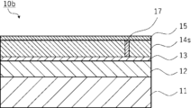
- FIG. 1 is a schematic diagram showing an example of a reflective mask blank of the present invention.
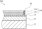
- FIG. 1 is a schematic diagram showing an example of a reflective mask blank of the present invention.
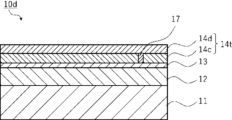
- FIG. 1 is a schematic diagram showing an example of a reflective mask blank of the present invention.
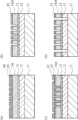
- FIG. 2 is a schematic diagram showing an example of a process for manufacturing a reflective mask using the reflective mask blank of the present invention.
- FIG. 3 is a schematic diagram for explaining processing errors in Examples.
- the reflective mask blank of the present invention is a reflective mask blank that includes a substrate, a multilayer reflective film that reflects EUV light, a protective film, and an absorber film in this order. has a sheet resistance value of 1.0 ⁇ 10 3 ⁇ /sq. between the outermost layer located on the opposite side and the protective film.
- the above insulating layer is arranged, and the interlayer electrical resistance value between the surface of the outermost layer opposite to the substrate side and the protective film is 100 k ⁇ or less.
- the inventors of the present invention speculate as follows.
- a charged particle beam is often used.
- the reflective mask blank for example, a layer of 1.0 ⁇ 10 3 ⁇ /sq.
- the above insulating layers may be arranged.
- the reflective mask blank of the present invention an insulating layer is disposed between the outermost layer and the protective film, and the interlayer electrical resistance value is 100 k ⁇ or less. That is, in the reflective mask blank of the present invention, charges easily move between the outermost layer and the protective film, and the outermost layer is less likely to be charged. As a result, it is estimated that the reflective mask blank of the present invention has smaller processing errors.
- FIG. 1 A first embodiment of the reflective mask blank of the present invention is shown in FIG.
- the reflective mask blank 10a shown in FIG. 1 includes a substrate 11, a multilayer reflective film 12, a protective film 13, an absorber film 14, and a conductive layer 15 in this order. Further, a side conductive portion 16 is arranged on the side surface of the absorber film 14 and the conductive layer 15. The side conductive portion 16 is in contact with the side surface of the conductive layer 15 and the surface of the protective film 13 .
- the absorber film 14 is composed of a first absorber film 14a and a second absorber film 14b from the substrate 11 side, and the second absorber film 14b has a sheet resistance value of 1.0 ⁇ 10 3 ⁇ /sq.
- the conductive layer 15 corresponds to the outermost layer located on the opposite side to the substrate 11 and closest to the surface.
- a second absorber film 14b corresponding to an insulating layer is disposed between the conductive layer 15, which is the outermost layer, and the protective film 13.
- the reflective mask blank 10a there is a side conductive part 16 disposed in contact with the side surface of the conductive layer 15 and the surface of the protective film 13, and the side conductive part 16 is arranged in contact with the conductive layer 15 and the surface of the protective film 13.
- the conductive layer which is the outermost layer It has been achieved that the interlayer electrical resistance value between the surface of layer 15 on the side opposite to substrate 11 and protective film 13 is 100 k ⁇ or less.
- the interlayer electrical resistance value even when the surface of the conductive layer 15 is processed using a charged particle beam, the charges in the conductive layer 15, which is the outermost layer, are transferred to the protective film 13. Therefore, charging of the conductive layer 15 is suppressed, and as a result, processing errors due to bending of the charged particle beam are less likely to occur.
- the interlayer electrical resistance value can be measured by the method shown below. First, a part of the protective film of the reflective mask blank is exposed by a method such as etching. The electrical resistance value between the exposed protective film and the surface of the outermost layer of the reflective mask blank on the side opposite to the substrate side is measured using a manual prober (manufactured by Hysol, model: HMP-400). . At this time, the straight distance in the plane direction of the substrate between the measurement terminal that is brought into contact with the protective film and the measurement terminal that is brought into contact with the outermost layer is set to 20 mm. According to the above method, when the electrical resistance value of the protective film is small, the interlayer electrical resistance value between the surface of the outermost layer opposite to the substrate side and the protective film can be measured.
- the interlayer electrical resistance value mainly depends on the electrical resistance value in the direction perpendicular to the substrate of the layer on the opposite side of the substrate side than the protective film, and the film thickness of that layer.
- the electrical resistance value of the substrate in the horizontal direction can be ignored. Therefore, even if the interlayer electrical resistance value is measured by changing the linear distance at the time of the measurement from 20 mm to 100 mm, the value will be equivalent to that in the case of 20 mm.
- the interlayer electrical resistance value is preferably 50 k ⁇ or less, more preferably 20 k ⁇ or less, even more preferably 10 k ⁇ or less, particularly preferably 1 k ⁇ or less, and most preferably 250 k ⁇ or less.
- the lower limit of the interlayer electrical resistance value is not particularly limited, but may be 0.01 ⁇ or more, often 50 ⁇ or more.
- the substrate included in the first embodiment of the reflective mask blank of the present invention preferably has a small coefficient of thermal expansion.
- the thermal expansion coefficient of the substrate at 20°C is preferably 0 ⁇ 1.0 ⁇ 10 ⁇ 7 /°C, more preferably 0 ⁇ 0.3 ⁇ 10 ⁇ 7 /°C.
- Materials with a small coefficient of thermal expansion include, but are not limited to, SiO 2 -TiO 2 glass, crystallized glass on which ⁇ -quartz solid solution is precipitated, quartz glass, metal silicon, and metal substrates. can also be used.
- SiO 2 -TiO 2 -based glass it is preferable to use silica glass containing 90 to 95% by mass of SiO 2 and 5 to 10% by mass of TiO 2 .
- the content of TiO 2 is 5 to 10% by mass, the linear expansion coefficient near room temperature is approximately zero, and almost no dimensional change occurs near room temperature.
- the SiO 2 -TiO 2 -based glass may contain trace components other than SiO 2 and TiO 2 .
- the surface of the substrate on which the multilayer reflective film is laminated (hereinafter also referred to as "first principal surface") has high surface smoothness.
- the surface smoothness of the first main surface can be evaluated by surface roughness.
- the surface roughness of the first principal surface is preferably root mean square roughness Rq of 0.15 nm or less. Note that the surface roughness can be measured using an atomic force microscope, and the surface roughness will be described as root mean square roughness Rq based on JIS-B0601.
- the first main surface is preferably surface-processed to have a predetermined flatness, since pattern transfer accuracy and positional accuracy of a reflective mask obtained using a reflective mask blank can be improved.
- the flatness of the substrate is preferably 100 nm or less, more preferably 50 nm or less, and even more preferably 30 nm or less in a predetermined area (for example, a 132 mm x 132 mm area) on the first main surface.
- the flatness can be measured using a flatness measuring device manufactured by Fujinon.
- the size, thickness, etc. of the substrate are appropriately determined based on the design values of the mask, etc.
- the outer shape may be 6 inches (152 mm) square, and the thickness may be 0.25 inches (6.3 mm).
- the substrate preferably has high rigidity in order to prevent deformation due to film stress of a film (multilayer reflective film, phase shift film, etc.) formed on the substrate.
- the Young's modulus of the substrate is preferably 65 GPa or more.
- the multilayer reflective film included in the first embodiment of the reflective mask blank of the present invention is not particularly limited as long as it has the desired characteristics as a reflective film for an EUV mask blank. It is preferable that the multilayer reflective film has a high reflectance for EUV light. Specifically, when EUV light is incident on the surface of the multilayer reflective film at an incident angle of 6°, EUV light with a wavelength of around 13.5 nm is reflected. The maximum value of the reflectance is preferably 60% or more, more preferably 65% or more. Furthermore, even when a protective film is laminated on the multilayer reflective film, the maximum reflectance of EUV light around a wavelength of 13.5 nm is preferably 60% or more, more preferably 65% or more. .
- a multilayer reflective film Since a multilayer reflective film can achieve a high reflectance of EUV light, it usually has a high refractive index layer that has a high refractive index for EUV light and a low refractive index layer that has a low refractive index for EUV light.
- a multilayer reflective film that is alternately laminated multiple times is used.
- the multilayer reflective film may be laminated in multiple periods, with one period having a laminated structure in which a high refractive index layer and a low refractive index layer are laminated in this order from the substrate side.
- a plurality of periods may be laminated, with a laminated structure laminated in sequence being one period.
- a layer containing Si can be used as the high refractive index layer.
- a Si compound containing Si and one or more selected from the group consisting of B, C, N, and O can be used.
- a high refractive index layer containing Si By using a high refractive index layer containing Si, a reflective mask with excellent reflectance for EUV light can be obtained.
- a layer containing a metal selected from the group consisting of Mo, Ru, Rh, and Pt, or an alloy thereof can be used.
- Si is widely used for the high refractive index layer
- Mo is widely used for the low refractive index layer. That is, Mo/Si multilayer reflective film is the most common.
- the multilayer reflective film is not limited to this, and includes Ru/Si multilayer reflective film, Mo/Be multilayer reflective film, Mo compound/Si compound multilayer reflective film, Si/Mo/Ru multilayer reflective film, and Si/Mo/Ru/ A Mo multilayer reflective film and a Si/Ru/Mo/Ru multilayer reflective film can also be used.
- each layer constituting the multilayer reflective film and the number of repeating units in the layer can be appropriately selected depending on the film material used and the EUV light reflectance required of the reflective layer.
- a Mo/Si multilayer reflective film as an example, in order to make a multilayer reflective film with a maximum EUV light reflectance of 60% or more, a Mo film with a film thickness of 2.3 ⁇ 0.1 nm and a film thickness of 4 .5 ⁇ 0.1 nm Si film may be laminated so that the number of repeating units is 30 to 60.
- each layer constituting the multilayer reflective film can be formed to a desired thickness using a known film forming method such as a magnetron sputtering method or an ion beam sputtering method.
- a known film forming method such as a magnetron sputtering method or an ion beam sputtering method.
- ion particles are supplied from an ion source to a target made of a high refractive index material and a target made of a low refractive index material.
- the multilayer reflective film is a Mo/Si multilayer reflective film
- a Si layer having a predetermined thickness is first formed on the substrate by ion beam sputtering using, for example, a Si target. Thereafter, a Mo layer having a predetermined thickness is formed using a Mo target.
- a Mo/Si multilayer reflective film is formed by laminating 30 to 60 cycles of the Si layer and Mo layer.
- the layer in contact with the protective film of the multilayer reflective film is preferably a layer made of a material that is difficult to oxidize.
- the layer made of a material that is not easily oxidized functions as a cap layer of the multilayer reflective film.
- An example of the layer made of a material that is difficult to oxidize is a Si layer.
- the layer in contact with the protective film functions as a cap layer. In that case, the thickness of the cap layer is preferably 11 ⁇ 2 nm.
- the protective film of the first embodiment of the reflective mask blank of the present invention prevents the multilayer reflective film from being damaged by the etching process when patterning the absorber film by an etching process (usually a dry etching process).
- an etching process usually a dry etching process.
- materials that can achieve the above object include materials containing at least one element selected from the group consisting of Ru and Rh. That is, the protective film preferably contains at least one element selected from the group consisting of Ru and Rh. More specifically, the above-mentioned materials include Ru metal alone, Ru alloy containing Ru and one or more metals selected from the group consisting of Si, Ti, Nb, Rh, and Zr, and Rh metal.
- materials that can achieve the above object include Al, nitrides containing these metals and nitrogen, and Al 2 O 3 .
- materials that can achieve the above object are preferably Ru metal alone, Ru alloy, Rh metal alone, or Rh alloy.
- As the Ru alloy a Ru--Si alloy is preferred, and as the Rh alloy, a Rh--Si alloy is preferred.
- the thickness of the protective film is not particularly limited as long as it can function as a protective film.
- the thickness of the protective film is preferably 1 to 10 nm, more preferably 1.5 to 6 nm, and even more preferably 2 to 5 nm.
- the material of the protective film is Ru metal alone, Ru alloy, Rh metal alone, or Rh alloy, and that the thickness of the protective film is the above-mentioned preferred thickness.
- the protective film may be a film consisting of a single layer or a multilayer film consisting of multiple layers.
- each layer constituting the multilayer film is preferably made of the above-mentioned preferred material.
- the protective film is a multilayer film, it is also preferable that the total film thickness of the multilayer film falls within the above-mentioned preferable range.
- the sheet resistance value of the protective film is 1.0 ⁇ 10 3 ⁇ /sq., since processing errors are smaller when processing with a charged particle beam. It is preferably less than 7.5 ⁇ 10 2 ⁇ /sq. The following is more preferable, 5.0 ⁇ 10 2 ⁇ /sq. The following are more preferred.
- the lower limit of the sheet resistance value of the protective film is not particularly limited, but is 1.0 ⁇ 10 ⁇ 1 ⁇ /sq. The above is mentioned, and 1.0 ⁇ 10 0 ⁇ /sq. The above is preferable.
- the sheet resistance value can be measured by bringing the measurement terminal into contact with the protective film using the four-probe method.
- the sheet resistance value can be measured with a surface resistivity meter (Loresta GX MCP-T700, manufactured by Nitto Seiko Analytech).
- the sheet resistance value of the protective film may be measured, for example, by exposing the protective film of a reflective mask blank by a method such as etching.
- the sheet resistance value of the protective film can be determined by analyzing the components and thickness of the protective film using a known analysis method (for example, transmission scanning electron microscopy - energy dispersive X-ray spectroscopy), and measuring the same components and thickness.
- the sample for measurement may be prepared on another substrate (for example, an insulating substrate) and then measured, or the sample for measurement may be prepared on another substrate (for example, an insulating substrate) under the same conditions as those for forming the protective film. It may also be prepared and measured.
- the sheet resistance value of the protective film may be measured using a laminate in the process of manufacturing a reflective mask blank, that is, for example, a sample in which a substrate, a multilayer reflective film, and a protective film are formed. According to the method described above, similar sheet resistance values can be obtained.
- the protective film can be formed using a known film forming method such as a magnetron sputtering method or an ion beam sputtering method.
- a known film forming method such as a magnetron sputtering method or an ion beam sputtering method.
- an Ru target as a target and Ar gas as a sputtering gas.
- the absorber film (the first absorber film and the second absorber film) included in the first embodiment of the reflective mask blank of the present invention is capable of absorbing EUV that is reflected by the multilayer reflective film when the absorber film is patterned. A high contrast between the light and the EUV light reflected by the absorber film is required.
- the patterned absorber film (absorber film pattern) may absorb EUV light and function as a binary mask, and may reflect EUV light while interfering with EUV light from the multilayer reflective film to create contrast. It may also function as a phase shift mask. Further, examples of the absorber film include a film having a so-called antireflection function.
- the layer disposed on the opposite side of the absorber film from the protective film side receives the inspection light (for example, wavelength 193 to 248 nm). It may also be an anti-reflection film when inspecting an absorber film pattern.
- materials constituting the absorber film include Cr, Co, Ni, Cu, Nb, Mo, Au, Ag, Ru, Rh, Pd, In, Sn, Hf, Ta, W, Re, Os, Ir, and A material containing at least one element (first element) selected from the group consisting of Pt is preferable.
- the absorber film When using an absorber film pattern as a binary mask, the absorber film must absorb EUV light and have a low reflectance of EUV light. Specifically, when the surface of the absorber film is irradiated with EUV light, the maximum reflectance of EUV light around a wavelength of 13.5 nm is preferably 2% or less.
- the absorber film (the first absorber film and the second absorber film) contains one or more elements selected from the group consisting of Ta, Ti, Sn, and Cr, and O, N, B, Hf, and H. It is preferable to include one or more elements selected from the group consisting of: Among these, it is preferable to include N or B.
- the crystalline state of the absorber film can be made into an amorphous or microcrystalline structure.
- the thickness of the absorber film is preferably 40 to 70 nm, more preferably 50 to 65 nm.
- the EUV light reflectance of the absorber film is preferably 2% or more. In order to obtain a sufficient phase shift effect, the EUV light reflectance of the absorber film is preferably 9 to 15%.
- Using an absorber film as a phase shift mask improves the contrast of the optical image on the wafer and increases the exposure margin.
- materials forming the phase shift mask include materials containing one or more elements selected from the group consisting of Cr, Nb, Ru, Ta, Re, Ir, Ag, Os, Au, Pd, and Pt. It will be done.
- the absorber film includes a first layer containing a first element selected from the group consisting of Ru, Re, Ir, Ag, Os, Au, Pd and Pt, and a first layer containing a first element selected from the group consisting of Nb, Ta and Cr. It is preferable to include a second layer containing two elements. It is also preferable that the first layer and the second layer contain at least one element selected from the group consisting of N, O, B, Si, and C. It is also preferable that the first layer corresponds to the above-mentioned first absorbent film, and the second layer corresponds to the above-mentioned second absorbent film.
- Examples of materials for forming the phase shift mask include simple substances of the above elements, alloys containing the above elements, oxides of the above elements, nitrides of the above elements, oxynitrides of the above elements, borides of the above elements, and borides of the above elements.
- materials for forming the phase shift mask include Ru metal alone, Ru nitride, Ru oxynitride, Ta nitride, Ta oxynitride, Ru and Cr, Au, Pt, Re, Hf, Ti, and Si.
- the material of the phase shift mask forming the layer in contact with the protective film is selected from a material different from the material forming the protective film.
- the thickness of the absorber film is preferably 30 to 60 nm, more preferably 35 to 55 nm.
- the crystalline state of the absorber film is preferably amorphous. This improves the smoothness and flatness of the absorber film. Furthermore, when the smoothness and flatness of the absorber film increases, the edge roughness of the absorber film pattern becomes smaller, and the dimensional accuracy of the absorber film pattern can be increased.
- the absorber film can be formed using a known film forming method such as magnetron sputtering or ion beam sputtering.
- a known film forming method such as magnetron sputtering or ion beam sputtering.
- the absorber film can be formed by performing sputtering using a Ru target and supplying a gas containing Ar gas and oxygen gas.
- the absorbent film 14 has a two-layer structure of a first absorbent film 14a and a second absorbent film 14b.
- the second absorber film 14b has a sheet resistance value of 1.0 ⁇ 10 3 ⁇ /sq. This is the layer.
- the second absorber film 14b functions as an absorber film and corresponds to an insulating layer whose sheet resistance value is equal to or greater than a predetermined value.
- the sheet resistance value can be measured by the same method as the method for measuring the sheet resistance value of the protective film.
- the material constituting the second absorber film 14b include a material containing the second element and an element selected from the group consisting of O and B. More specifically, Ta oxide, Ta oxynitride, Ta boride, Ta oxyboride, Cr oxide, Cr oxynitride, and Cr oxyboride can be mentioned.
- the thickness of the second absorber film 14b is preferably 50 nm or less, more preferably 30 nm or less.
- the lower limit is not particularly limited, but may be 1 nm or more, often 5 nm or more.
- the sheet resistance value of the first absorber film 14a is 1.0 ⁇ 10 3 ⁇ /sq. It is preferably less than 7.5 ⁇ 10 2 ⁇ /sq. The following is more preferable, 5.0 ⁇ 10 2 ⁇ /sq. The following are more preferred.
- the lower limit of the sheet resistance value of the first absorber film 14a is not particularly limited, but may be 1.0 ⁇ 10 ⁇ 1 ⁇ or more, preferably 1.0 ⁇ 10 0 ⁇ or more.
- the sheet resistance value can be measured by the same method as the method for measuring the sheet resistance value of the protective film.
- the material constituting the first absorber film 14a is exemplified by, for example, a material containing the above-mentioned first element.
- Ru metal alone Ru nitride, Ru oxide, Ru oxynitride, Ru boride, Ir metal alone, Ir nitride, Ir oxide, Ir oxynitride, Ir boride, Ta nitride. and Pt metal alone.
- the conductive layer of the first embodiment of the reflective mask blank of the present invention is also the outermost layer located on the surface side of the reflective mask blank opposite to the substrate.
- the sheet resistance value of the conductive layer is 1.0 ⁇ 10 3 ⁇ /sq. It is preferably less than 7.5 ⁇ 10 2 ⁇ /sq. The following is more preferable, 5.0 ⁇ 10 2 ⁇ /sq. The following are more preferred.
- the lower limit of the sheet resistance value of the conductive layer is not particularly limited, but is 1.0 ⁇ 10 ⁇ 1 ⁇ /sq. The above is mentioned, and 1.0 ⁇ 10 0 ⁇ /sq. The above is preferable.
- the sheet resistance value can be measured according to the method for measuring the sheet resistance value of a protective film.
- the materials constituting the outermost conductive layer include Ti, Cr, Co, Ni, Cu, Zr, Nb, Mo, Ru, Rh, Pd, In, Sn, Hf, Ta, W, Re, Os, At least one element (first metal element) selected from the group consisting of Ir and Pt is included. Moreover, it is preferable that the conductive layer, which is the outermost layer, contains one or more elements (first nonmetallic element) selected from the group consisting of N, O, B, Si, and C. The conductive layer, which is the outermost layer, may contain the first metal element and the first non-metal element.
- the conductive layer included in the first embodiment of the reflective mask blank of the present invention may be a hard mask film.
- the elements contained in the material constituting the hard mask film include the first metal elements mentioned above, including Ti, Cr, Co, Ni, Cu, Zr, Nb, Mo, Ru, Rh, Pd, In, Sn, and Hf. , Ta, and Ir are preferred.
- the hard mask film it is preferable to use a material with high resistance to dry etching, such as a Si-based film, a Cr-based film, a Nb-based film, a Mo-based film, a Ru-based film, and a Ta-based film.
- the hard mask film is preferably a film made of a material containing the above element and one or more elements selected from the group consisting of O, N, C, B, and H, and is made of a material containing the above element and N and C.
- a film made of a material containing one or more elements selected from the group is more preferable.
- a material containing Cr and O will also be written as "CrO”
- a material containing Cr, O, and N will also be written as "CrON”.
- Examples of the material constituting the Cr-based film include Cr (single Cr), CrC, CrB, CrBN, CrO, CrN, and CrON, with Cr or CrN being preferred.
- Examples of the material constituting the Nb-based film include Nb (Nb alone), NbC, NbB, NbBN, NbO, NbN, and NbON, with Nb or NbN being preferred.
- Examples of the material constituting the Mo-based film include Mo (Mo alone), MoC, MoB, MoBN, MoO, MoN, and MoON, with Mo or MoN being preferred.
- Examples of the material constituting the Ru-based film include Ru (Ru alone), RuC, RuB, RuBN, RuO, RuN, and RuON, with RuO, RuN, and RuON being preferred.
- Examples of the material constituting the Ta-based film include Ta (single Ta), TaC, TaB, TaBN, TaO, TaN, and TaON, with Ta or TaN being preferred.
- the thickness of the hard mask film is preferably 1 to 20 nm, more preferably 5 to 15 nm.
- the hard mask film can be formed by a known film forming method, for example, by a magnetron sputtering method or an ion beam sputtering method.
- a reaction using a Ru target is performed in a gas atmosphere containing a mixture of an inert gas containing at least one of He, Ar, Ne, Kr, and Xe, oxygen gas, and nitrogen gas.
- a physical sputtering method may be used.
- the insulating layer of the first embodiment of the reflective mask blank of the present invention has a sheet resistance value of 1.0 ⁇ 10 3 ⁇ /sq. These are the layers above.
- the second absorber film 14b corresponds to the insulating layer.
- the thickness of the insulating layer is preferably 50 nm or less, more preferably 30 nm or less. The lower limit is not particularly limited, but may be 1 nm or more, often 5 nm or more.
- the sheet resistance value of the layer adjacent to the insulating layer is 1.0 ⁇ 10 3 ⁇ /sq. It is preferably less than 7.5 ⁇ 10 2 ⁇ /sq. The following is more preferable, 5.0 ⁇ 10 2 ⁇ /sq. The following are more preferred.
- the sheet resistance of the conductive layer 15 and the first absorber film 14a is the above-mentioned preferable value.
- the side conductive portion of the first embodiment of the reflective mask blank of the present invention is arranged on the side surfaces of the absorber film and the conductive layer.
- the side conductive portion is in contact with the side surface of the conductive layer and the surface of the protective film, and is a member that ensures electrical continuity between the conductive layer, which is the outermost layer, and the protective film.
- the side conductive portion 16 includes the first absorber film 14a and the conductive layer 15, which are arranged adjacently on both sides of the second absorber film 14b, which is an insulating layer, and the conductive layer 15, which is an insulating layer. , are in contact with the protective film 13.
- the material constituting the side conductive portion includes, for example, at least one element selected from the group consisting of Li, B, C, F, Na, Mg, Al, Si, K, Ca, Sn, and transition metal elements. It is preferable. In particular, from the viewpoint of productivity, it is preferable that the material forming the side conductive portion is the same as the material forming the conductive layer.
- the method for forming the side conductive part is not particularly limited, but for example, a multilayer reflective layer, a protective film, an absorber film, and a conductive layer are formed on the substrate, and then the material constituting the side face conductive part is sputtered, etc. It can be formed using the following method. Note that when the side conductive portion is made of the same material as the conductive layer, the side conductive portion may be formed simultaneously with the formation of the conductive layer. More specifically, for example, first, a multilayer reflective film and a protective film are formed on the substrate in this order.
- the absorber film is formed by limiting the region in which the absorber film is to be formed so that the end portion of the absorber film to be formed is closer to the center of the substrate than the end portion of the formed protective film.
- a conductive layer is formed on the absorber film, and at the same time, a side conductive portion made of the same material as the conductive layer is formed on the side surface of the absorber film.
- a more detailed manufacturing procedure will be shown in the latter part.
- the first embodiment of the reflective mask blank of the present invention may have a back conductive film on the surface (second main surface) opposite to the first main surface of the substrate.
- the reflective mask blank can be handled using an electrostatic chuck.
- the back conductive film has a low sheet resistance value.
- the sheet resistance value of the back conductive film is, for example, 200 ⁇ /sq.
- the following is preferable, 100 ⁇ /sq.
- the constituent material of the back conductive film can be selected from a wide range of materials described in known literature. For example, a high dielectric constant coating described in Japanese Patent Publication No.
- the constituent material of the back conductive film is a Cr compound containing Cr and one or more selected from the group consisting of B, N, O, and C, or a Cr compound containing Ta and one or more selected from the group consisting of B, N, O, and C. It may also be a Ta compound containing one or more selected from the group consisting of:
- the thickness of the back conductive film is preferably 10 to 1000 nm, more preferably 10 to 400 nm. Further, the back conductive film may have a function of adjusting stress on the second main surface side of the reflective mask blank.
- the back conductive film can be adjusted to flatten the reflective mask blank by balancing stress from various films formed on the first main surface side.
- the back conductive film can be formed using a known film forming method, for example, a sputtering method such as a magnetron sputtering method or an ion beam sputtering method, a CVD method, a vacuum evaporation method, or an electrolytic plating method.
- the absorber film has a two-layer structure, but the present invention is not limited to this embodiment.
- the absorber film may have a structure of three or more layers, and any one of the layers may correspond to the above-mentioned insulating layer.
- the absorber film may have a single layer structure, and the single layer itself may correspond to the above-mentioned insulating layer.
- all layers included in the absorber film may be insulating layers.
- any of the layers located between the outermost layer and the protective film may be any of the above-mentioned insulating layers, and unlike the embodiment shown in FIG.
- an insulating layer may be included as another member.
- the present invention is not limited to this embodiment as long as the value is within a predetermined range.
- the sheet resistance value of the first absorber film 14a is 1.0 ⁇ 10 3 ⁇ /sq. If it is less than 1, the side conductive portion may be disposed so as to cover at least the side surface of the second absorber film 14b, which is an insulating layer, and to be in contact with the conductive layer 15 and the first absorber film 14a.
- the conductive layer 15 disposed adjacent to both sides of the first absorber film 14a, which is an insulating layer, and the first absorber film 14a can be electrically connected by the side conductive portions, and as described above.
- the interlayer electrical resistance value was achieved. That is, it is preferable that the side conductive portion is disposed at least on the side surface of the insulating layer and contacts layers disposed adjacent to each other on both sides of the insulating layer to ensure conduction between the two.
- the body membrane and the ends of the conductive layer are located at the center of the substrate, the invention is not limited to this embodiment.
- the positions of the ends of the protective film, the absorbent film, and the conductive layer may be substantially coincident, and the side conductive portions may be arranged on the side surfaces of the protective film, the absorbent film, and the conductive layer.
- the positions of the ends of the substrate, the multilayer reflective film, the protective film, the absorber film, and the conductive layer may substantially coincide with each other, and the side conductive portions may be arranged on all sides of the reflective mask blank.
- FIG. 2 A second embodiment of the reflective mask blank of the present invention is shown in FIG.
- the reflective mask blank 10b shown in FIG. 2 includes a substrate 11, a multilayer reflective film 12, a protective film 13, an absorber film 14s, and a conductive layer 15 in this order. Further, a through conductive portion 17 that penetrates in the thickness direction is arranged in the absorber film 14s. Penetrating conductive portion 17 is in contact with conductive layer 15 and protective film 13 .
- the absorber film 14s has a sheet resistance value of 1.0 ⁇ 10 3 ⁇ /sq. This corresponds to the insulating layer described above.
- the conductive layer 15 corresponds to the outermost layer located on the opposite side to the substrate 11 and closest to the surface.
- an absorber film 14s corresponding to an insulating layer is disposed between the conductive layer 15, which is the outermost layer, and the protective film 13.
- the conductive layer 15, which is the outermost layer even if the absorber film 14s, which is an insulating layer, is disposed between the conductive layer 15, which is the outermost layer, and the protective film 13, the conductive layer 15, which is the outermost layer, It has been achieved that the interlayer electrical resistance value between the surface opposite to the substrate 11 side and the protective film 13 is 100 k ⁇ or less.
- the interlayer electrical resistance value between the surface opposite to the substrate 11 side and the protective film 13 is 100 k ⁇ or less.
- the method for measuring the interlayer electrical resistance value between the outermost layer and the protective film in the second embodiment of the reflective mask blank of the present invention is the method for measuring the interlayer electrical resistance value described in the first embodiment of the reflective mask blank. is the same as Further, the preferred range of the interlayer electrical resistance value in the second embodiment of the reflective mask blank of the present invention is the same as the preferred range of the interlayer electrical resistance value described in the first embodiment of the reflective mask blank.
- the reflective mask blank 10b shown in FIG. 2 does not have a side conductive part but has a through conductive part. Since they have the same configuration, a description of the same configuration will be omitted, and in the latter part, only the through conductive portion will be mainly described.
- the through conductive portion included in the second embodiment of the reflective mask blank of the present invention is provided within the absorber film, which is an insulating layer.
- the through conductive portion is a member that is in contact with the surface of the conductive layer and the surface of the protective film, and ensures electrical continuity between the conductive layer, which is the outermost layer, and the protective film. More specifically, in FIG. 2, the through conductive portion 17 is in contact with the protective film 13 and the conductive layer 15, which are arranged adjacently on both sides of the absorber film 14s, which is an insulating layer.
- the material constituting the through conductive portion includes, for example, at least one element selected from the group consisting of Li, B, C, F, Na, Mg, Al, Si, K, Ca, Sn, and transition metal elements. It is preferable. In particular, from the viewpoint of productivity, it is preferable that the material forming the through-hole conductive portion is the same as the material forming the conductive layer.
- the through conductive portion 17 is provided at only one location, but the conductive portion may be provided at two or more locations.
- the shape of the through conductive portion is not particularly limited, and may be any one of a columnar shape, a polygonal columnar shape, a conical shape, a polygonal pyramid shape, a truncated cone shape, a truncated polygonal pyramid shape, a spherical shape, a polyhedral shape, and the like.
- the maximum width in cross section of the through conductive portion is preferably 1 nm to 100 ⁇ m, more preferably 10 nm to 15 ⁇ m.
- the through conductive portion 17 is filled with the material that constitutes the through conductive portion in the cross section of the through conductive portion 17, but if electrical continuity between the conductive layer and the protective film can be ensured,
- the through conductive portion does not need to be completely filled with the material constituting the through conductive portion. That is, in the cross section of the through conductive part, it is sufficient that a part of the material constituting the through conductive part exists, and there may be a hollow part or a part where another material exists.
- the method of forming the through conductive portion is not particularly limited, but for example, a method of forming a through hole in the insulating layer during or after forming the insulating layer (the absorber film in FIG. 2), and then forming a conductive layer. can be mentioned.
- the through conductive portion is formed of the same material as the material forming the conductive layer.
- particles having a height equal to or greater than the thickness of the insulating layer to be formed are placed on the surface of the layer forming the insulating layer.
- There is also a method of arranging and forming an insulating layer. Examples of the method for arranging the particles include a method in which pre-generated particles are placed on the surface of the layer forming the insulating layer using a manipulator or the like.
- the absorber film is composed of one layer, but the present invention is not limited to this embodiment. That is, the absorbent film may be a multilayer film (multilayer absorbent film) consisting of two or more layers. If the absorber film is a multilayer film and one or more layers constituting the absorber film correspond to an insulating layer, the through conductive part corresponds to an insulating layer among the layers constituting the absorber film. It is arranged so as to penetrate the layer in the thickness direction.
- the absorber film is an insulating layer, but the present invention is not limited to this embodiment.
- an embodiment may be adopted in which an insulating layer is included as a member separate from the absorber film.
- the sheet resistance value of the layer adjacent to the insulating layer is 1.0 ⁇ 10 3 ⁇ /sq. It is preferably less than 7.5 ⁇ 10 2 ⁇ /sq. The following is more preferable, 5.0 ⁇ 10 2 ⁇ /sq. The following are more preferred.
- the sheet resistance of the conductive layer 15 and the protective film 13 is the above-mentioned preferable value.
- the second embodiment of the reflective mask blank of the present invention may have a back conductive film on the surface (second main surface) opposite to the first main surface of the substrate.
- the configuration of the back conductive film is as described in the first embodiment of the reflective mask blank described above.
- FIG. 3 A third embodiment of the reflective mask blank of the present invention is shown in FIG.
- the reflective mask blank 10c shown in FIG. 3 includes a substrate 11, a multilayer reflective film 12, a protective film 13, and an absorber film 14t in this order. Furthermore, a side conductive portion 16 is arranged on the side surface of the absorber film 14t. The side conductive portion 16 is in contact with the side surface of the absorber film 14t and the surface of the protective film 13.
- the absorber film 14t is composed of a first absorber film 14c and a second absorber film 14d from the substrate 11 side, and the first absorber film 14c has a sheet resistance value of 1.0 ⁇ 10 3 ⁇ /sq. This corresponds to the insulating layer described above.
- the sheet resistance value of the second absorber film 14d is 1.0 ⁇ 10 3 ⁇ /sq. less than Further, in the reflective mask blank 10c, the second absorber film 14d corresponds to the outermost layer (upper layer) located at the outermost surface side on the opposite side from the substrate 11. In the reflective mask blank 10c shown in FIG. 3, a first absorber film 14c corresponding to an insulating layer is disposed between a second absorber film 14d, which is the outermost layer, and the protective film 13. On the other hand, in the reflective mask blank 10c, there is a side conductive portion 16 disposed in contact with the side surface of the second absorber film 14d and the surface of the protective film 13. The conductivity between the protective film 13 and the protective film 13 is ensured.
- the first absorber film 14c which is an insulating layer
- the first absorber film 14c which is the outermost layer
- the interlayer electrical resistance value between the surface of the 2-absorber film 14d on the side opposite to the substrate 11 side and the protective film 13 is 100 k ⁇ or less.
- the method for measuring the interlayer electrical resistance value between the outermost layer and the protective film in the third embodiment of the reflective mask blank of the present invention is the method for measuring the interlayer electrical resistance value described in the first embodiment of the reflective mask blank. is the same as Further, the preferred range of the interlayer electrical resistance value in the third embodiment of the reflective mask blank of the present invention is the same as the preferred range of the interlayer electrical resistance value described in the first embodiment of the reflective mask blank.
- the absorber film has a two-layer structure of a first absorber film 14c and a second absorber film 14d.
- the first absorber film 14c has a sheet resistance value of 1.0 ⁇ 10 3 ⁇ /sq. This is the layer. That is, the first absorbent film 14c is a layer that functions as an absorbent film and has a sheet resistance value equal to or greater than a predetermined value. The sheet resistance value can be measured by the same method as the method for measuring the sheet resistance value of the protective film.
- the material constituting the first absorber film 14c include a material containing the second element and O. More specifically, Ta oxide, Ta oxynitride, and Ta oxyboride, or Cr oxide, Cr oxynitride, and Cr oxyboride are mentioned.
- the sheet resistance value of the second absorber film 14d is 1.0 ⁇ 10 3 ⁇ /sq. It is preferably less than 7.5 ⁇ 10 2 ⁇ /sq. The following is more preferable, 5.0 ⁇ 10 2 ⁇ /sq. The following are more preferred.
- the lower limit of the sheet resistance value of the second absorber film 14d is not particularly limited, but is 1.0 ⁇ 10 0 ⁇ /sq. The above is mentioned, and 1.0 ⁇ 10 1 ⁇ /sq. The above is preferable.
- the sheet resistance value can be measured by the same method as the method for measuring the sheet resistance value of the protective film.
- the material constituting the second absorber film 14d is exemplified by, for example, a material containing the above-mentioned first element.
- the materials constituting the second absorber film 14d include Ru metal alone, Ru nitride, Ru oxide, Ru oxynitride, Ru boride, Ir metal alone, Ir nitride, and Ir oxide. , Ir oxynitride, Ir boride, Ta nitride, and simple Pt metal.
- the side conductive portion is arranged on the side surface of the absorber film.
- the side conductive portion is in contact with the side surface of the absorber film and the surface of the protective film, and is a member that ensures electrical continuity between the second absorber film, which is the outermost layer, and the protective film. More specifically, in FIG. 3, the side conductive portion 16 is in contact with the second absorber film 14d and the protective film 13, which are arranged adjacently on both sides of the first absorber film 14c, which is an insulating layer. ing.
- the material constituting the side conductive portion includes, for example, at least one element selected from the group consisting of Li, B, C, F, Na, Mg, Al, Si, K, Ca, Sn, and transition metal elements. It is preferable. In particular, from the viewpoint of productivity, it is preferable that the material forming the side conductive portion is the same as the material forming the conductive layer.
- the method for forming the side conductive part is not particularly limited, but for example, a multilayer reflective layer, a protective film, and an absorber film are formed on the substrate, and then the material constituting the side conductive part is formed by a method such as sputtering. do it.
- the side conductive portion is made of the same material as the second absorber film, the side conductive portion may be formed simultaneously with the formation of the second absorber film. More specifically, for example, first, a multilayer reflective film and a protective film are formed on the substrate in this order. Next, the area in which the first absorber film is formed is limited so that the end of the first absorber film to be formed is closer to the center of the substrate than the end of the formed protective film, and the first absorber film is formed.
- a second absorber film is formed on the first absorber film, and at the same time, a side conductive portion made of the same material as the second absorber film is formed on the side surface of the first absorber film. form. In addition, a more detailed manufacturing procedure will be shown in the latter part.
- the absorber film has a two-layer structure, but the present invention is not limited to this embodiment.
- the absorber film may have a structure of three or more layers, and any one of the layers may correspond to the above-mentioned insulating layer.
- the absorber film may have a three-layer structure, a first absorber film, a second absorber film, and a third absorber film are arranged from the substrate side, and the second absorber film is an insulating layer, good.
- the third absorbent film corresponds to the upper layer.
- the sheet resistance value of the layer adjacent to the insulating layer is 1.0 ⁇ 10 3 ⁇ /sq.
- the sheet resistance of the second absorbent film 14d and the protective film 13 be the above-mentioned preferable values.
- the end of the absorber film is located closer to the center of the substrate than the end of the protective film.
- the invention is not limited to this embodiment.
- the positions of the end portions of the protective film and the absorber film may be substantially coincident, and the side conductive portion may be arranged on the side surface of the absorber film.
- the positions of the ends of the substrate, the multilayer reflective film, the protective film, the absorber film, and the conductive layer may substantially coincide with each other, and the side conductive portions may be arranged on all sides of the reflective mask blank.
- the third embodiment of the reflective mask blank of the present invention may have a back conductive film on the surface (second main surface) opposite to the first main surface of the substrate.
- the configuration of the back conductive film is as described in the first embodiment of the reflective mask blank described above.
- FIG. 4 A fourth embodiment of the reflective mask blank of the present invention is shown in FIG.
- the reflective mask blank 10d shown in FIG. 4 includes a substrate 11, a multilayer reflective film 12, a protective film 13, and an absorber film 14t in this order.
- the absorber film 14t is composed of a first absorber film 14c and a second absorber film 14d from the substrate 11 side, and the first absorber film 14c has a sheet resistance value of 1.0 ⁇ 10 3 ⁇ /sq. This corresponds to the insulating layer described above.
- the sheet resistance value of the second absorber film 14d is 1.0 ⁇ 10 3 ⁇ /sq.
- the second absorber film 14d corresponds to the outermost layer (upper layer) located on the outermost side of the surface opposite to the substrate 11. Further, a through conductive portion 17 that penetrates in the thickness direction is arranged in the first absorber film 14c. The through conductive portion 17 is in contact with the second absorber film 14d and the protective film 13. In the reflective mask blank 10d shown in FIG. 4, a first absorber film 14c, which corresponds to an insulating layer, is arranged between a second absorber film 14d, which is the outermost layer, and the protective film 13.
- the reflective mask blank 10d there is a through conductive portion 17 that penetrates the first absorber film 14c in the thickness direction, and the through conductive portion 17 is located between the second absorber film 14d and the protective film 13. Ensures conductivity. Therefore, in the reflective mask blank 10d, even if the first absorber film 14c, which is an insulating layer, is disposed between the second absorber film 14d, which is the outermost layer, and the protective film 13, the first absorber film 14c, which is the outermost layer, It has been achieved that the interlayer electrical resistance value between the surface of the second absorber film 14d opposite to the substrate 11 side and the protective film 13 is 100 k ⁇ or less.
- the method for measuring the interlayer electrical resistance value between the outermost layer and the protective film in the fourth embodiment of the reflective mask blank of the present invention is the method for measuring the interlayer electrical resistance value described in the first embodiment of the reflective mask blank. is the same as Further, the preferred range of the interlayer electrical resistance value in the fourth embodiment of the reflective mask blank of the present invention is the same as the preferred range of the interlayer electrical resistance value described in the first embodiment of the reflective mask blank.
- the reflective mask blank 10d shown in FIG. 4 does not have a side conductive part but has a through conductive part. Since they have the same configuration, a description of the same configuration will be omitted, and in the latter part, only the through conductive portion will be mainly described.
- the through conductive portion included in the fourth embodiment of the reflective mask blank of the present invention is provided within the first absorber film, which is an insulating layer.
- the through conductive portion is in contact with the surface of the second absorbent film and the surface of the protective film, and is a member that ensures electrical continuity between the second absorbent film, which is the outermost layer, and the protective film. More specifically, in FIG. 4, the through conductive portion 17 is in contact with the protective film 13 and the second absorber film 14d, which are arranged adjacently on both sides of the first absorber film 14c, which is an insulating layer. ing.
- the material constituting the through conductive portion includes, for example, at least one element selected from the group consisting of Li, B, C, F, Na, Mg, Al, Si, K, Ca, Sn, and transition metal elements. It is preferable. In particular, from the viewpoint of productivity, it is preferable that the material forming the through-hole conductive portion is the same as the material forming the conductive layer.
- the through conductive portion 17 is provided at only one location, but the conductive portion may be provided at two or more locations.
- the shape of the conductive through portion and the maximum width in the cross section of the conductive through portion are preferably the same as the preferred aspect of the conductive through portion in the second embodiment.
- the method for forming the through conductive portion is not particularly limited, but for example, a through hole may be provided in the insulating layer during or after the formation of the insulating layer (the first absorber film in FIG. 4), and then a conductive layer may be formed.
- a through hole may be provided in the insulating layer during or after the formation of the insulating layer (the first absorber film in FIG. 4), and then a conductive layer may be formed.
- the through conductive portion is formed of the same material as the material forming the conductive layer.
- particles having a height equal to or greater than the thickness of the insulating layer to be formed are placed on the surface of the layer forming the insulating layer.
- the absorber film has a two-layer structure, but the present invention is not limited to this embodiment.
- the absorber film may have a structure of three or more layers, and any one of the layers may correspond to the above-mentioned insulating layer.
- a first absorber film, a second absorber film, and a third absorber film are arranged from the substrate side, and the second absorber film is an insulating layer, good.
- the through conductive portion is arranged to penetrate through the second insulating layer in the thickness direction.
- the third absorbent film corresponds to the upper layer.
- the first absorber film is an insulating layer, but the present invention is not limited to this embodiment.
- an embodiment may be adopted in which an insulating layer is included as a member separate from the absorber film.
- the sheet resistance of the layer adjacent to the insulating layer is 1.0 ⁇ 10 3 ⁇ /sq. It is preferably less than 7.5 ⁇ 10 2 ⁇ /sq. The following is more preferable, 5.0 ⁇ 10 2 ⁇ /sq. The following are more preferred.
- the sheet resistance values of the second absorbent film 14d and the protective film 13 are preferably the above-mentioned preferred values.
- the fourth embodiment of the reflective mask blank of the present invention may have a back conductive film on the surface (second main surface) opposite to the first main surface of the substrate.
- the configuration of the back conductive film is as described in the first embodiment of the reflective mask blank described above.
- a substrate, a multilayer reflective film that reflects EUV light, a protective film, and an absorber film having a single-layer structure or a multi-layer structure are formed in this order.
- the sheet resistance value is 1.0 ⁇ 10 3 ⁇ /sq. on the absorber film side than the protective film.
- the sheet resistance value of the laminate including the above insulating layer on the absorber film is 1.0 ⁇ 10 3 ⁇ /sq.
- the present invention includes a step of forming a conductive layer exhibiting less than or equal to 100 nm, and forming a side conductive portion that covers at least the side surface of the insulating layer and is electrically connected to the conductive layer.
- a first embodiment of the method for manufacturing a reflective mask blank of the present invention will be described with reference to FIG. 1.
- a multilayer reflective film 12 that reflects EUV light, a protective film 13, an absorber film 14, and a conductive layer 15 are provided on a substrate 11 in this order.
- a reflective mask blank 10a in which side conductive portions 16 are disposed on the side surfaces of conductive layer 15 can be manufactured.
- a substrate 11 is prepared, and a multilayer reflective film 12 is formed on the substrate 11.
- the multilayer reflective film 12 can be formed by the method described above, and each layer constituting the multilayer reflective film is formed to a desired thickness using a known film forming method such as magnetron sputtering or ion beam sputtering. can.
- a protective film 13 is formed on the multilayer reflective film 12.
- the protective film 13 can be formed by the method described above, and can be formed by a known film forming method such as magnetron sputtering method or ion beam sputtering method.
- an absorber film 14 is formed on the protective film 13.
- the absorber film 14 can be formed by the method described above, or by using a known film forming method such as magnetron sputtering or ion beam sputtering. It is also preferable that the absorber film 14 formed corresponds to the above-mentioned insulating layer.
- the region where the absorber film 14 is formed is narrower than the region where the protective film 13 is formed.
- a mask is provided to cover a part of the protective film 13 to limit the area where the absorber film 14 is formed. A method of forming a film may be mentioned.
- the mask that covers part of the protective film 13 is preferably an end mask that covers a certain area from the end of the protective film 13.
- the end mask preferably covers 0.05 to 5.0 mm from the end of the protective film 13, and preferably covers 0.1 to 1.0 mm.
- the end mask may cover a part of the end of the protective film 13, or may cover all of the end of the protective film 13.
- a conductive layer 15 is formed on the absorber film 14.
- the sheet resistance value of the conductive layer 15 to be formed is 1.0 ⁇ 10 3 ⁇ /sq. less than The sheet resistance value can be measured by the method described above.
- a side conductive portion 16 is formed that covers at least the side surface of the insulating layer (second absorber film) and is electrically connected to the conductive layer. Formation of the conductive layer 15 and formation of the side conductive portions 16 may be performed simultaneously or separately, but from the viewpoint of productivity, it is preferable to perform them simultaneously.
- An example of this method is to arrange at least a portion of the target to be used and form the side conductive portions 16 on the side surfaces of the absorber film 14.
- Another method is to make the region where the absorber film 14 is formed narrower than the protective film 13 using the edge mask etc., and then form the conductive layer 15 without using the edge mask etc.
- One method is to do so.
- Another method is to make the region where the absorber film 14 is formed narrower than the protective film 13 using the edge mask, etc., so that the opening is smaller than the mask used to form the absorber film 14.
- a method of forming the conductive layer 15 using a large mask can be mentioned. Another method is to make the area where the absorber film 14 is formed narrower than the protective film 13 by using the end mask, etc., and rotate the end mask by about 0.1 to 10 degrees to form a conductive film. A method for forming the layer 15 may be mentioned. According to the method described above, the same material as the conductive layer 15 is formed not only on the upper surface of the absorber film 14 but also on the side surfaces of the absorber film 14, so that the side surfaces of the absorber film 14 are formed with the conductive layer 15. Covered with similar material.
- the first embodiment of the method for manufacturing a reflective mask blank of the present invention it is possible to manufacture a reflective mask blank with small processing errors when processed using a charged particle beam.
- the preferred embodiments of the reflective mask blank to be manufactured and the preferred embodiments of each configuration are as described above.
- the reflective mask blank to be manufactured may be a reflective mask blank having a mode other than that shown in FIG. 1 as described above.
- a second embodiment of the method for manufacturing a reflective mask blank of the present invention includes, in this order, a substrate, a multilayer reflective film that reflects EUV light, a protective film, and a single-layer or multi-layer absorber film.
- the sheet resistance value is 1.0 ⁇ 10 3 ⁇ /sq. on the absorber film side than the protective film.
- the sheet resistance value of the laminate including the above insulating layer on the absorber film is 1.0 ⁇ 10 3 ⁇ /sq.
- the present invention includes a step of forming an upper layer exhibiting less than or equal to 100% as a part of the absorbing film body, and forming a side conductive portion that covers at least the side surface of the insulating layer and is electrically connected to the upper layer.
- a second embodiment of the method for manufacturing a reflective mask blank of the present invention will be described with reference to FIG. 3.
- a multilayer reflective film 12 that reflects EUV light, a protective film 13, and an absorber film 14t are provided on the substrate 11 in this order, and the absorber film 14t is disposed on the protective film 13 side.
- a reflective film is composed of a first absorber film 14c arranged on the side opposite to the protective film 13, and a second absorber film 14d arranged on the side opposite to the protective film 13, and a side conductive part 16 is arranged on the side surface of the absorber film 14.
- a mold mask blank 10c can be manufactured.
- the first absorber film 14c has a sheet resistance value of 1.0 ⁇ 10 3 ⁇ /sq.
- the second absorber film 14d corresponds to the above-mentioned insulating layer, and the second absorber film 14d corresponds to the above-mentioned upper layer, and the sheet resistance value of the second absorber film 14d is 1.0 ⁇ 10 3 ⁇ /sq. less than
- a substrate 11 is prepared, and a multilayer reflective film 12 is formed on the substrate 11.
- the multilayer reflective film 12 can be formed by the method described above, and each layer constituting the multilayer reflective film is formed to a desired thickness using a known film forming method such as magnetron sputtering or ion beam sputtering. can.
- a protective film 13 is formed on the multilayer reflective film 12.
- the protective film 13 can be formed by the method described above, and can be formed by a known film forming method such as magnetron sputtering or ion beam sputtering.
- the first absorber film 14c is formed on the protective film 13.
- the first absorber film 14c can be formed by the method described above, and can be formed by using a known film forming method such as magnetron sputtering or ion beam sputtering. It is also preferable that the first absorber film 14c formed corresponds to the above-mentioned insulating layer.
- the region where the first absorbent film 14c is formed is narrower than the region where the protective film 13 is formed.
- the method of narrowing the region where the first absorber film 14c is formed and its preferred mode are the same as the method of narrowing the region where the absorber film 14 is formed and its preferred mode described in the first embodiment. Therefore, the explanation will be omitted.
- a second absorbent film 14d is formed on the first absorbent film 14c.
- the sheet resistance value of the second absorber film 14d to be formed is 1.0 ⁇ 10 3 ⁇ /sq. less than The sheet resistance value can be measured by the method described above.
- a side conductive portion 16 is formed that covers at least the side surface of the insulating layer (first absorber film 14c) and is electrically connected to the second absorber film 14d.
- the formation of the second absorber film 14d and the formation of the side conductive portions 16 may be performed simultaneously or separately, but from the viewpoint of productivity, it is preferable to perform them simultaneously.
- the second absorber film 14d can be formed by the method described above, or by using a known film forming method such as magnetron sputtering or ion beam sputtering.
- the second absorber film 14d is formed at the end of the first absorber film 14c in a direction opposite to the center side of the substrate 11.
- An example of this method is to arrange at least a part of the target used in forming the film 14d and form the side conductive portion 16 on the side surface of the first absorber film 14c.
- Another method is to make the area where the first absorber film 14c is formed narrower than the protective film 13 using the edge mask etc.
- An example of this method is to form the second absorber film 14d in this state.
- Another method is to make the area where the first absorber film 14c is formed narrower than the protective film 13 using the end mask described in the first embodiment, and form the first absorber film 14c.
- a method of forming the second absorber film 14d using a mask having a larger opening than the mask used for forming the film is exemplified.
- Another method is to make the area where the first absorber film 14c is formed narrower than the protective film 13 by using the end mask described in the first embodiment, and adjust the end mask to 0.1 to
- a method of forming the second absorber film 14d by rotating it by about 10 degrees is exemplified.
- the same material as the second absorber film 14d is formed not only on the top surface of the first absorber film 14c but also on the side surfaces of the first absorber film 14c, and the first absorber film 14c The side surfaces of the absorbent film 14d are coated with the same material as the second absorbent film 14d.
- the second embodiment of the method for manufacturing a reflective mask blank of the present invention it is possible to manufacture a reflective mask blank with small processing errors when processed using a charged particle beam.
- the preferable aspect of the reflective mask blank manufactured and the preferable aspect of each structure are as each mentioned above.
- the reflective mask blank to be manufactured may be a reflective mask blank in a mode other than that shown in FIG. 3 as described above.
- the absorber film may have a structure of three or more layers, and any one of the layers may correspond to the above-mentioned insulating layer.
- the absorber film has a three-layer structure, a first absorber film, a second absorber film, and a third absorber film are arranged from the substrate side, and the second absorber film is an insulating layer, good.
- the third absorber film corresponds to the above-mentioned upper layer, and the sheet resistance value of the third absorber film is 1.0 ⁇ 10 3 ⁇ /sq. less than
- the reflective mask is obtained by patterning the absorber film included in the reflective mask blank of the present invention.
- An example of a method for manufacturing a reflective mask will be described with reference to FIG. Note that, although a method for manufacturing a reflective mask using the reflective mask blank 10b of the second embodiment described in FIG. can.
- FIG. 5A shows a state in which a resist pattern 40 is formed on a reflective mask blank having a substrate 11, a multilayer reflective film 12, a protective film 13, an absorber film 14s, and a conductive layer 15 in this order. show.
- a known method can be used to form the resist pattern 40. For example, a resist is applied onto the conductive layer 15 of a reflective mask blank, and exposed and developed to form the resist pattern 40. Note that the resist pattern 40 corresponds to a pattern formed on a wafer using a reflective mask. Thereafter, using the resist pattern 40 in FIG. 5(a) as a mask, the absorber film 14s and the conductive layer 15 are etched and patterned, and the resist pattern 40 is removed. A laminate having a film pattern 14pt is obtained.
- the conductive layer 15 corresponds to a hard mask film
- the conductive layer 15 disposed in the opening of the resist pattern 40 is removed by etching, and the absorber film is removed by etching. 14s may be etched and patterned.
- a resist pattern 41 corresponding to the frame of the exposure area is formed on the laminate shown in FIG. 5B, and the resist pattern 41 in FIG. 5C is masked. Perform dry etching as follows. Dry etching is performed until the substrate 11 is reached. After dry etching, the resist pattern 41 is removed to obtain a reflective mask shown in FIG. 5(d).
- Examples of the dry etching used to form the absorber film pattern 14pt include dry etching using a Cl-based gas and dry etching using an F-based gas.
- the conductive layer 15 disposed in the opening of the resist pattern 40 may be etched by wet etching using a chemical solution or by dry etching. It is also preferable to select a method for etching the conductive layer 15 in which the conductive layer 15 is etched but the absorber film 14s is not etched.
- the resist pattern 40 or 41 may be removed by a known method, such as using a cleaning solution.
- cleaning liquid examples include sulfuric acid-hydrogen peroxide aqueous solution (SPM), sulfuric acid, aqueous ammonia, ammonia-hydrogen peroxide aqueous solution (APM), OH radical cleaning water, and ozone water.
- SPM sulfuric acid-hydrogen peroxide aqueous solution
- APM ammonia-hydrogen peroxide aqueous solution
- OH radical cleaning water ozone water.
- the reflective mask obtained by patterning the phase shift film of the reflective mask blank of the present invention can be suitably applied as a reflective mask used for exposure with EUV light.
- a reflective mask blank of Example 1 was manufactured according to the following procedure.
- a SiO 2 -TiO 2 -based glass substrate (outer size: 152 mm square, thickness: approximately 6.3 mm) was used.
- This glass substrate has a coefficient of thermal expansion of 0.2 ⁇ 10 ⁇ 7 /° C., a Young's modulus of 67 GPa, a Poisson's ratio of 0.17, and a specific rigidity of 3.07 ⁇ 10 7 m 2 /s 2 .
- the glass substrate was used after being polished so that the surface roughness (root mean square height Sq) of the main surface was 0.15 nm or less and the flatness was 100 nm or less.
- a CrN layer with a thickness of about 100 nm was formed using a magnetron sputtering method to form a back conductive film for an electrostatic chuck. .
- the sheet resistance value of the CrN layer is approximately 100 ⁇ /sq. Met.
- the glass substrate was fixed in a film forming chamber by electrostatic adsorption.
- a multilayer reflective film was formed on the first main surface (processed surface) of the glass substrate.
- an ion beam sputtering method was used to deposit a Mo layer with a thickness of 2.3 nm and a Si layer with a thickness of 4.5 nm 40 times alternately.
- a film was formed.
- the Mo layer was formed by ion beam sputtering using a Mo target in an Ar gas atmosphere (gas pressure: 0.02 Pa).
- the applied voltage was 700 V, and the film formation rate was 3.84 nm/min.
- the Si layer ion beam sputtering was performed in an Ar gas atmosphere using a boron-doped Si target (gas pressure: 0.02 Pa).
- the applied voltage was 700 V, and the film formation rate was 4.62 nm/min.
- the protective film had a two-layer structure consisting of an Ru layer and a Rh layer in order from the substrate side.
- the Ru layer was formed by ion beam sputtering using an Ru target in an Ar gas atmosphere (gas pressure: 0.02 Pa).
- the applied voltage was 700 V, and the film formation rate was 3.12 nm/min.
- the thickness of the Ru layer was 1.0 nm.
- the Rh layer was formed by ion beam sputtering using an Rh target in an Ar gas atmosphere (gas pressure: 0.027 Pa).
- the applied voltage was 600 V, and the film formation rate was 4.62 nm/min.
- the thickness of the Rh layer was 1.5 nm.
- an absorber film was formed on the protective film by ion beam sputtering and magnetron sputtering.
- the absorber film had a three-layer structure consisting of a RuN layer, a TaN layer, and a TaON layer in order from the substrate side. Note that the absorber film was formed in a 148 mm square area by partially masking it.
- magnetron sputtering was performed using a Ru target in an atmosphere of a mixed gas of Ar gas and N2 gas (Ar gas: 80% by volume, N2 gas: 20% by volume) (gas Pressure: 0.2 Pa).
- the applied voltage was 700 V, and the film formation rate was 3.0 nm/min.
- the thickness of the RuN layer was 29 nm.
- the TaN layer magnetron sputtering was performed using a Ta target in an atmosphere of a mixed gas of Ar gas and N2 gas (Ar gas: 95% by volume, N2 gas: 5% by volume). .
- the film formation rate was 1.74 nm/min, and the thickness of the TaN layer was 8 nm.
- a Ta target was used to form a mixed gas of Ar gas, N 2 gas, and O 2 gas (Ar gas: 60% by volume, N 2 gas: 30% by volume, O 2 gas: 10% by volume).
- Magnetron sputtering was carried out in an atmosphere of %).
- the film formation rate was 0.6 nm/min, and the thickness of the TaON layer was 14 nm.
- a conductive layer was formed on the absorber film by magnetron sputtering.
- This conductive layer corresponds to a hard mask film.
- the conductive layer was an Ru layer. Note that the conductive layer was formed in a 149 mm square area by partially masking.
- the Ru layer was formed by ion beam sputtering using an Ru target in an Ar gas atmosphere (gas pressure: 0.2 Pa).
- the applied voltage was 700 V, and the film formation rate was 3.0 nm/min.
- the thickness of the Ru layer was 10 nm.
- a side conductive portion was formed that covered the side surface of the absorber film and the side surface of the conductive layer and was in contact with the surface of the protective film.
- a reflective mask blank of Example 1 was obtained by the above procedure.
- the sheet resistance values of the conductive layers of the reflective mask blanks of Example 1 and Examples 2 to 7 to be described later were measured by the above method, and the results are shown in the table below.
- the reflective mask blank of Example 2 was manufactured in the same manner as the reflective mask blank of Example 1, except that the conductive layer was a RuN layer.
- the conditions for forming the RuN layer were the same as those for the RuN layer described above, and the thickness of the RuN layer was 10 nm.
- the reflective mask blank of Example 3 was manufactured in the same manner as the reflective mask blank of Example 1, except that the conductive layer was a CrN layer.
- ion beam sputtering was performed using a Cr target in an atmosphere of a mixed gas of Ar gas and N2 gas (Ar gas: 85% by volume, N2 gas: 15% by volume) ( Gas pressure: 0.2 Pa).
- the film formation rate was 1.6 nm/min.
- the thickness of the CrN layer was 10 nm.
- the reflective mask blank of Example 4 was manufactured in the same manner as the reflective mask blank of Example 1, except that the conductive layer was a TaN layer.
- the conditions for forming the TaN layer were the same as those for forming the TaN described above, and the thickness of the TaN layer was 10 nm. Note that the TaN layer formed as a conductive layer corresponds to an absorber film.
- the reflective mask blank of Example 5 was manufactured using the following procedure. First, in the same way as the reflective mask blank of Example 2, a multilayer reflective film, a protective film, and an absorber film were formed. However, the absorber film was formed on the entire surface of the protective film without using a mask. After forming the absorber film, a 10 ⁇ m square hole was formed in the absorber film, with the center position being 7.1 mm away from one corner of the substrate toward the center of the substrate. The holes were formed so that the RuN layer of the absorber film was exposed. Note that a focused ion beam processing device, which will be described later, was used to form the holes.
- the reflective mask blank of Example 6 was manufactured in the same manner as the reflective mask blank of Example 1, except that no conductive layer was provided. In the reflective mask blank of Example 6, no side conductive portions were formed.
- a multilayer reflective film was first formed on the substrate in the same manner as the reflective mask blank of Example 1.
- a protective film was formed on the multilayer reflective film by high frequency sputtering.
- the protective film was an SiO layer.
- the SiO layer was formed by high frequency sputtering in an Ar gas atmosphere using a SiO 2 target.
- the thickness of the SiO layer was 2.6 nm.
- the absorber film was formed on the protective film by magnetron sputtering.
- the absorber film had a two-layer structure consisting of a RuCrON layer and a RuCrO layer in order from the substrate side.
- the RuCrON layer was formed using a Ru target and a Cr target, using a mixed gas of Ar gas and N2 gas (Ar gas: 70% by volume, N2 gas: 20% by volume, O2 gas: 10% by volume). ) Magnetron sputtering was performed in an atmosphere of The thickness of the RuCrON layer was 33.5 nm.
- the RuCrO layer was formed by magnetron sputtering using a Ru target and a Cr target in an atmosphere of a mixed gas of Kr gas and O 2 gas (Ar gas: 50 volume %, O 2 gas: 50 volume %). was carried out.
- the thickness of the RuCrO layer was 8.5 nm.
- a hard mask film was formed on the absorber film by magnetron sputtering.
- the hard mask film was a SiN layer.
- the SiN layer was formed by magnetron sputtering in an N2 gas atmosphere using a Si target.
- the thickness of the SiN layer was 20 nm.
- a reflective mask blank of Example 7 was obtained by the above procedure.
- the protective film was exposed by bringing the area where the protective film was to be exposed into contact with the treatment solution heated to 80° C. for 30 minutes. After the contact, the sample was rinsed with pure water and dried to obtain a sample to be used for interlayer electrical resistance measurement. In the treatment using the treatment liquid, the Rh layer is not dissolved and exposed.
- the reflective mask blank of Example 6 after contacting with 85% by mass phosphoric acid at 160°C for 30 minutes, it was contacted with 9% by mass diammonium cerium (IV) nitrate and 6% by mass at 25°C. A solution containing perchloric acid was brought into contact with the sample for 30 minutes to obtain a sample for measurement of interlayer electrical resistance.
- an absorber film or the like was formed by masking the same area as the area where the above-mentioned protective film was exposed, and the protective film was exposed.
- a sample to be used for measuring the interlayer electrical resistance value was also prepared. When the interlayer electrical resistance values of the sample formed by masking as described above and the sample obtained by etching were compared, no significant difference was confirmed.
- Processing errors of the reflective mask blanks of each example were evaluated using the following procedure.
- the reflective mask blank was processed with a charged particle beam to form a shape for evaluation using a focused ion beam processing device (manufactured by Hitachi High-Tech Corporation, model number SMI3050R). Ga was used as the ion species of the ion beam to be irradiated, and the acceleration voltage was 30 kV.
- the design shape of the evaluation shape was a rectangular parallelepiped with a length of 1 ⁇ m, a width of 10 ⁇ m, and a depth of 0.1 ⁇ m.
- the processing conditions of the focused ion beam processing apparatus were such that the above-mentioned shape for evaluation could be accurately formed for the sample in which the reflective mask blank of Example 1 was formed up to the Ru layer of the protective film.
- an observation sample was prepared in which a Pt film was formed as an antistatic coating for a scanning electron microscope.
- the shape of the processed area was observed using a field emission scanning electron microscope (manufactured by Hitachi High-Technology, S-4800) from a direction perpendicular to the first principal surface of the substrate of the observation sample.
- the design shape of the evaluation shape and the shape of the machining area were compared to evaluate the machining error.
- FIG. 6 is a schematic diagram of an observation example when evaluating processing errors in the example.
- the area indicated by a dashed line is a virtual area representing the designed shape 30, and the area indicated by a solid line is a processed area 32 formed by processing.
- the protruding portion 34A is an area outside the area of the designed shape 30 and within the area of the processing area 32.
- the chipped portion 34S is an area within the area of the designed shape 30 and outside the area of the processing area 32.
- the area S A of the protruding portion in the above formula is the total area of the protruding portion 34A.
- the area S S of the chipped portion is the total area of the chipped portion 34S.
- the processing error was evaluated based on the above processing error E (%) using the following criteria. Practically speaking, an evaluation of A or B is preferable.
- Table 1 shows the layer structure, sheet resistance value, interlayer electrical resistance value, and processing error evaluation results for each example. Note that the sheet resistance value of each layer was measured by the method described above using a sample formed up to each layer.
- the "insulating layer sheet resistance value” column shows the layer corresponding to the insulating layer and its sheet resistance value. Note that when there are two or more layers corresponding to the insulating layer, the layer with the largest sheet resistance value is described as the insulating layer.
- the description ">40M” in the "Outermost layer sheet resistance value” column and the “Insulating layer sheet resistance value” column means that the sheet resistance value is 40M ⁇ /sq. This indicates that the above was the case.
- “k” in the description of "50k” represents the SI prefix "kilo”, and the sheet resistance value is 50 k ⁇ /sq. It means that it was.
Landscapes
- Physics & Mathematics (AREA)
- General Physics & Mathematics (AREA)
- Chemical & Material Sciences (AREA)
- Chemical Kinetics & Catalysis (AREA)
- Engineering & Computer Science (AREA)
- Materials Engineering (AREA)
- Mechanical Engineering (AREA)
- Metallurgy (AREA)
- Organic Chemistry (AREA)
- Preparing Plates And Mask In Photomechanical Process (AREA)
- Exposure Of Semiconductors, Excluding Electron Or Ion Beam Exposure (AREA)
Abstract
Description
なお、上記吸収体膜のパターニングの際に、多層反射膜を保護する目的で、多層反射膜と吸収体膜との間に保護膜が設けられることも多い。
また、反射型マスクのマスクパターンの修正のため、荷電粒子線による吸収体膜の加工が実施される場合がある。
ここで、半導体デバイスの更なる微細化に対応するため、荷電粒子線を用いた加工において、より加工誤差が小さい反射型マスクブランクが求められている。
また、本発明は、反射型マスクブランクの製造方法の提供も課題とする。
また、本発明は、反射型マスク、および、反射型マスクの製造方法の提供も課題とする。
〔1〕 基板と、
EUV光を反射する多層反射膜と、
保護膜と、
単層構造または複層構造の吸収体膜とをこの順で有する反射型マスクブランクであって、
上記反射型マスクブランク中の上記基板とは反対側の最も表面側に位置する最表層と、上記保護膜との間に位置する層のいずれかが、シート抵抗値が1.0×10³Ω/sq.以上を示す絶縁層であり、
上記最表層の上記基板側とは反対側の表面と、上記保護膜との間の層間電気抵抗値が、100kΩ以下である、反射型マスクブランク。
〔2〕 上記吸収体膜上に、シート抵抗値が1.0×10³Ω/sq.未満である導電性層がさらに配置され、上記導電性層が上記最表層である、〔1〕に記載の反射型マスクブランク。
〔3〕 上記吸収体膜が、上記絶縁層に対応する層を含む、〔2〕に記載の反射型マスクブランク。
〔4〕 上記吸収体膜が、複層構造であり、
上記吸収体膜中の最も上記基板とは離れた位置にある上層のシート抵抗値が1.0×10³Ω/sq.未満であり、上記上層が上記最表層である、〔1〕に記載の反射型マスクブランク。
〔5〕 上記吸収体膜が、上記絶縁層に対応する層を含む、〔4〕に記載の反射型マスクブランク。
〔6〕 上記保護膜のシート抵抗値が、1.0×10³Ω/sq.未満である、〔1〕~〔5〕のいずれか一つに記載の反射型マスクブランク。
〔7〕 上記絶縁層の厚みが30nm以下である、〔1〕~〔6〕のいずれか一つに記載の反射型マスクブランク。
〔8〕 上記最表層と上記保護膜との間に、上記絶縁層の両側にそれぞれ隣接して配置される層同士を導通させる導電部を有する、〔1〕~〔7〕のいずれか一つに記載の反射型マスクブランク。
〔9〕 少なくとも上記絶縁層の側面に、上記導電部に対応する側面導電部が配置され、
上記側面導電部は、少なくとも、上記絶縁層の両側にそれぞれ隣接して配置される層と接触している、〔8〕に記載の反射型マスクブランク。
〔10〕 上記側面導電部が、上記最表層と上記保護膜との間に位置する全ての層の側面に配置される、〔9〕に記載の反射型マスクブランク。
〔11〕 上記絶縁層内に、厚み方向に貫通し、上記導電部に対応する貫通導電部が配置される、〔8〕に記載の反射型マスクブランク。
〔12〕 上記導電部が、リチウム、ホウ素、炭素、フッ素、ナトリウム、マグネシウム、アルミニウム、ケイ素、カリウム、カルシウム、錫および遷移金属元素からなる群から選択される少なくとも1種の元素を含む、〔8〕~〔11〕のいずれか一つに記載の反射型マスクブランク。
〔13〕 上記最表層が、チタン、クロム、コバルト、ニッケル、銅、ジルコニウム、ニオブ、モリブデン、ルテニウム、ロジウム、パラジウム、インジウム、錫、ハフニウム、タンタル、タングステン、レニウム、オスミウム、イリジウムおよび白金からなる群から選択される少なくとも1種の元素を含む、〔1〕~〔12〕のいずれか一つに記載の反射型マスクブランク。
〔14〕 上記最表層が、窒素、酸素、ホウ素、ケイ素および炭素からなる群から選択される少なくとも1種の元素を含む、〔1〕~〔13〕のいずれか一つに記載の反射型マスクブランク。
〔15〕 〔1〕~〔14〕のいずれか1つに記載の反射型マスクブランクの上記吸収体膜をパターニングして形成される吸収体膜パターンを有する、反射型マスク。
〔16〕 〔1〕~〔14〕のいずれか1つに記載の反射型マスクブランクの上記吸収体膜をパターニングする工程を含む、反射型マスクの製造方法。
〔17〕 基板と、EUV光を反射する多層反射膜と、保護膜と、単層構造または複層構造の吸収体膜とをこの順で有し、上記保護膜よりも上記吸収体膜側にシート抵抗値が1.0×10³Ω/sq.以上を示す絶縁層を含む積層体の、上記吸収体膜上にシート抵抗値が1.0×103Ω/sq.未満を示す導電性層を形成し、かつ、上記絶縁層の側面を少なくとも覆い、上記導電性層と導通する側面導電部を形成する工程を有する、反射型マスクブランクの製造方法。
〔18〕 基板と、EUV光を反射する多層反射膜と、保護膜と、単層構造または複層構造の吸収体膜とをこの順で有し、上記保護膜よりも上記吸収体膜側にシート抵抗値が1.0×10³Ω/sq.以上を示す絶縁層を含む積層体の、上記吸収体膜上にシート抵抗値が1.0×103Ω/sq.未満を示す上層を吸収膜体の一部として形成し、かつ、上記絶縁層の側面を少なくとも覆い、上記上層と導通する側面導電部を形成する工程を有する、反射型マスクブランクの製造方法。
また、本発明によれば、反射型マスクブランクの製造方法も提供できる。
また、本発明によれば、反射型マスク、および、反射型マスクの製造方法も提供できる。
以下に記載する構成要件の説明は、本発明の代表的な実施態様に基づいてなされる場合があるが、本発明はそのような実施態様に制限されない。
本明細書において、「~」を用いて表される数値範囲は、「~」の前後に記載される数値を下限値および上限値として含む範囲を意味する。
本明細書において、各元素は、それぞれ対応する元素記号で表す場合がある。
本発明の反射型マスクブランクは、基板と、EUV光を反射する多層反射膜と、保護膜と、吸収体膜とをこの順で有する反射型マスクブランクであって、反射型マスクブランクの基板とは反対側の最も表面側に位置する最表層と、保護膜との間に、シート抵抗値が1.0×10³Ω/sq.以上の絶縁層が配置され、最表層の基板側とは反対側の表面と、保護膜との間の層間電気抵抗値が、100kΩ以下である。
反射型マスクブランクを加工する際(特に、吸収体膜のパターニングを行う際)には、荷電粒子線を用いる場合が多い。
一方、反射型マスクブランクにおいて、例えば、プラズマエッチングでエッチングされにくい層として、最表層と、保護膜との間に、1.0×10³Ω/sq.以上の絶縁層が配置されることがある。
反射型マスクブランクが上記のような絶縁層を有する場合、荷電粒子線による加工を続けていくと、最表層は、荷電粒子線の荷電粒子が有する電荷の符号と同じ符号に帯電しやすい。最表層が荷電粒子の電荷の符号と同じ符号に帯電すると、荷電粒子と、最表層との間で反発力が生じ、荷電粒子線が曲がり、加工誤差が生じやすいと考えられる。特に、絶縁層が反射型マスクブランクの最表層に位置する際に、上記問題が顕著に生じやすい。
ここで、本発明の反射型マスクブランクでは、最表層と、保護膜との間に絶縁層が配置されるが、層間電気抵抗値が100kΩ以下である。つまり、本発明の反射型マスクブランクにおいては、最表層と保護膜との間で電荷が移動しやすく、最表層が帯電しにくい。結果として、本発明の反射型マスクブランクは、加工誤差が小さくなると推測される。
本発明の反射型マスクブランクの第1実施態様を図1に示す。
図1に示す、反射型マスクブランク10aは、基板11と、多層反射膜12と、保護膜13と、吸収体膜14と、導電性層15とをこの順に有する。また、吸収体膜14および導電性層15の側面に、側面導電部16が配置されている。側面導電部16は、導電性層15の側面および保護膜13の表面と接している。吸収体膜14は、基板11側から第1吸収体膜14aと、第2吸収体膜14bとから構成され、第2吸収体膜14bはシート抵抗値が1.0×10³Ω/sq.以上を示す絶縁層に該当する。また、反射型マスクブランク10aにおいて、導電性層15が、基板11とは反対側の最も表面側に位置する最表層に該当する。
図1に示す、反射型マスクブランク10aにおいては、最表層である導電性層15と、保護膜13との間に、絶縁層に該当する第2吸収体膜14bが配置されている。一方で、反射型マスクブランク10aにおいては、導電性層15の側面と保護膜13の表面と接して配置される側面導電部16が存在し、側面導電部16が導電性層15と保護膜13との間の導電性を確保している。従って、反射型マスクブランク10aにおいては、最表層である導電性層15と保護膜13との間において、絶縁層である第2吸収体膜14bが配置されていても、最表層である導電性層15の基板11側とは反対側の表面と、保護膜13との間の層間電気抵抗値が100kΩ以下であることが達成されている。このような層間電気抵抗値が達成されることにより、導電性層15の表面から荷電粒子線による加工がなされた際においても、最表層である導電性層15中の電荷が保護膜13に移動しやすく、導電性層15の帯電が抑制され、結果として、荷電粒子線の曲がりによる加工誤差が生じにくい。
まず、反射型マスクブランクの保護膜の一部の領域を、エッチング等の方法で露出させる。露出させた保護膜と、反射型マスクブランクの最表層の基板側とは反対側の表面との間の電気抵抗値を、マニュアルプローバー(ハイソル社製、型式:HMP-400)を用いて測定する。この際、保護膜に接触させる測定端子と、最表層に接触させる測定端子の基板平面方向の直線距離が、20mmとなるようにする。
なお、上記方法によれば、保護膜の電気抵抗値が小さい場合、最表層の基板側とは反対側の表面と、保護膜との間の層間電気抵抗値が測定できる。
また、保護膜の電気抵抗値が小さい場合、層間電気抵抗値は、主に保護膜よりも基板側とは反対側に存在する層の基板垂直方向の電気抵抗値およびその層の膜厚に依存し、基板の水平方向の電気抵抗値は無視できる。したがって、上記測定時の直線距離を20mmから100mmに変更して層間電気抵抗値を測定しても、20mmの場合と同等の値となる。
本発明の反射型マスクブランクの第1実施態様が有する基板は、熱膨張係数が小さいことが好ましい。基板の熱膨張係数が小さい方が、EUV光による露光時の熱により、吸収体膜パターンに歪みが生じることを抑制できる。
基板の熱膨張係数は、20℃において、0±1.0×10⁻⁷/℃が好ましく、0±0.3×10-7/℃がより好ましい。
熱膨張係数が小さい材料としては、SiO2-TiO2系ガラス等が挙げられるが、これに限定されず、β石英固溶体を析出した結晶化ガラス、石英ガラス、金属シリコン、および、金属等の基板も使用できる。
SiO2-TiO2系ガラスは、SiO2を90~95質量%、TiO2を5~10質量%含む石英ガラスを用いることが好ましい。TiO2の含有量が5~10質量%であると、室温付近での線膨張係数が略ゼロであり、室温付近での寸法変化がほとんど生じない。なお、SiO2-TiO2系ガラスは、SiO2およびTiO2以外の微量成分を含んでもよい。
第1主面は、反射型マスクブランクを用いて得られる反射型マスクのパターン転写精度および位置精度を高められる点で、所定の平坦度となるように表面加工されることが好ましい。基板は、第1主面の所定の領域(例えば、132mm×132mmの領域)において、平坦度は、100nm以下が好ましく、50nm以下がより好ましく、30nm以下がさらに好ましい。平坦度は、フジノン社製平坦度測定器によって測定できる。
基板の大きさおよび厚さ等は、マスクの設計値等により適宜決定される。例えば、外形は6インチ(152mm)角、および、厚さは0.25インチ(6.3mm)等が挙げられる。
さらに、基板は、基板上に形成される膜(多層反射膜、位相シフト膜等)の膜応力による変形を防止する点で、高い剛性を有することが好ましい。例えば、基板のヤング率は、65GPa以上が好ましい。
本発明の反射型マスクブランクの第1実施態様が有する多層反射膜は、EUVマスクブランクの反射膜として所望の特性を有する限り特に限定されない。多層反射膜は、EUV光に対して高い反射率を有することが好ましく、具体的には、EUV光が入射角6°で多層反射膜の表面に入射した際、波長13.5nm付近のEUV光の反射率の最大値は、60%以上が好ましく、65%以上がより好ましい。また、多層反射膜の上に、保護膜が積層されている場合でも、同様に、波長13.5nm付近のEUV光の反射率の最大値は、60%以上が好ましく、65%以上がより好ましい。
多層反射膜は、高屈折率層と低屈折率層とを基板側からこの順に積層した積層構造を1周期として複数周期積層してもよいし、低屈折率層と高屈折率層とをこの順に積層した積層構造を1周期として複数周期積層してもよい。
高屈折率層としては、Siを含む層を用いることができる。Siを含む材料としては、Si単体の他に、Siに、B、C、N、およびOからなる群から選択される1種以上を含むSi化合物を用いることができる。Siを含む高屈折率層を用いることによって、EUV光の反射率に優れた反射型マスクが得られる。
低屈折率層としては、Mo、Ru、Rh、およびPtからなる群から選択される金属、またはこれらの合金を含む層を用いることができる。
上記高屈折率層には、Siが広く使用され、低屈折率層にはMoが広く使用される。すなわち、Mo/Si多層反射膜が最も一般的である。但し、多層反射膜はこれに限定されず、Ru/Si多層反射膜、Mo/Be多層反射膜、Mo化合物/Si化合物多層反射膜、Si/Mo/Ru多層反射膜、Si/Mo/Ru/Mo多層反射膜、Si/Ru/Mo/Ru多層反射膜も使用できる。
本発明の反射型マスクブランクの第1実施態様が有する保護膜は、エッチングプロセス(通常はドライエッチングプロセス)により吸収体膜にパターン形成する際に、多層反射膜がエッチングプロセスによるダメージを受けないよう、多層反射膜を保護する目的で設けられる。
上記目的を達成できる材料としては、Ru、および、Rhからなる群から選択される少なくとも1つの元素を含む材料が挙げられる。すなわち、保護膜は、Ru、および、Rhからなる群から選択される少なくとも1つの元素を含むことが好ましい。
より具体的には、上記材料として、Ru金属単体、Ruと、Si、Ti、Nb、Rh、および、Zrからなる群から選択される1種以上の金属とを含むRu合金、ならびに、Rh金属単体、Rhと、Si、Ti、Nb、Rh、Ta、および、Zrからなる群から選択される1種以上の金属とを含むRh合金、上記Rh合金と窒素とを含むRh含有窒化物、および、上記Rh合金と窒素と酸素とを含むRh含有酸窒化物等のRh系材料が挙げられる。
また、上記目的を達成できる材料として、Alおよびこれらの金属と窒素とを含む窒化物、および、Al2O3等も例示される。
なかでも、上記目的を達成できる材料としては、Ru金属単体、Ru合金、Rh金属単体、または、Rh合金が好ましい。Ru合金としては、Ru-Si合金が好ましく、Rh合金としては、Rh-Si合金が好ましい。
保護膜の材料が、Ru金属単体、Ru合金、Rh金属単体、または、Rh合金であって、保護膜の膜厚が上記好ましい膜厚であることも好ましい。
シート抵抗値は、四探針法で保護膜に測定端子を接触させて測定できる。より具体的には、シート抵抗値は、表面抵抗率計(日東精工アナリテック社製、ロレスタGX MCP-T700)で測定できる。
保護膜のシート抵抗値は、例えば、反射型マスクブランクの保護膜を、エッチング等の方法で露出させて測定してもよい。また、保護膜のシート抵抗値は、保護膜の成分および厚さを公知の分析方法(例えば、透過型走査電子顕微鏡-エネルギー分散型X線分光)で分析し、同様の成分および厚さの測定用サンプルを他の基板(例えば絶縁性の基板)上に作製して測定してもよいし、保護膜の作製条件と同様の条件で測定用サンプルを他の基板(例えば絶縁性の基板)上に作製して測定してもよい。
なお、保護膜のシート抵抗値は、反射型マスクブランクを製造する途中の状態の積層体、すなわち、例えば、基板、多層反射膜および保護膜を形成したサンプルを用いて測定してもよい。
上述した方法によれば、同様のシート抵抗値が得られる。
本発明の反射型マスクブランクの第1実施態様が有する吸収体膜(第1吸収体膜および第2吸収体膜)は、吸収体膜をパターン化した際に、多層反射膜で反射されるEUV光と、吸収体膜で反射されるEUV光とのコントラストが高いことが求められる。
パターン化された吸収体膜(吸収体膜パターン)は、EUV光を吸収してバイナリマスクとして機能してもよく、EUV光を反射しつつ多層反射膜からのEUV光と干渉してコントラストを生じせしめる位相シフトマスクとして機能してもよい。
また、吸収体膜としては、いわゆる反射防止機能を有する膜も挙げられる。つまり、吸収体膜が多層膜(複層構造の吸収体膜)である場合、吸収体膜の保護膜側とは反対側に配置される層は、検査光(例えば、波長193~248nm)を用いて吸収体膜パターン検査する際の反射防止膜であってもよい。
吸収体膜を構成する材料としては、例えば、Cr、Co、Ni、Cu、Nb、Mo、Au、Ag、Ru、Rh、Pd、In、Sn、Hf、Ta、W、Re、Os、IrおよびPtからなる群から選択される少なくとも1種の元素(第1元素)を含む材料が好ましい。
吸収体膜(第1吸収体膜および第2吸収体膜)は、Ta、Ti、SnおよびCrからなる群から選択される1種以上の元素と、O、N、B、Hf、および、Hからなる群から選択される1種以上の元素とを含むことが好ましい。これらの中でも、NまたはBを含むことが好ましい。NまたはBを含むことで、吸収体膜の結晶状態をアモルファスまたは微結晶の構造にできる。
吸収体膜パターンをバイナリマスクとして用いる場合、吸収体膜の膜厚は、40~70nmが好ましく、50~65nmがより好ましい。
位相シフトマスクを形成する材料としては、例えば、Cr、Nb、Ru、Ta、Re、Ir、Ag、Os、Au、PdおよびPtからなる群から選択される1種以上の元素を含む材料が挙げられる。
吸収体膜は、Ru、Re、Ir、Ag、Os、Au、PdおよびPtからなる群から選択される第1元素を含む第1層と、Nb、TaおよびCrからなる群から選択される第2元素を含む第2層とを含むことが好ましい。上記第1層および第2層は、N、O、B、SiおよびCからなる群から選択される少なくとも1種の元素を含むことも好ましい。第1層が上記第1吸収体膜に該当し、第2層が上記第2吸収体膜に該当することも好ましい。
位相シフトマスクを形成する材料としては、例えば、上記元素の単体、上記元素を含む合金、上記元素の酸化物、上記元素の窒化物、上記元素の酸窒化物、上記元素のホウ化物、上記元素のケイ化物(シリサイド)、および、上記元素の炭化物、ならびに、上記元素を1種以上含む複合酸化物、上記元素を1種以上含む複合窒化物、上記元素を1種以上含む複合酸窒化物、上記元素を1種以上含む複合ホウ化物、上記元素を1種以上含む複合ケイ化物、および、上記元素を1種以上含む複合炭化物が挙げられる。
例えば、位相シフトマスクを形成する材料としては、Ru金属単体、Ru窒化物、Ru酸窒化物、Ta窒化物、Ta酸窒化物、RuとCr、Au、Pt、Re、Hf、TiおよびSiからなる群から選択される1種以上の金属とを含むRu合金、TaとNbとの合金、Ru合金またはTaNb合金と酸素とを含む酸化物、Ru合金またはTaNb合金と窒素とを含む窒化物、Ru合金またはTaNb合金と酸素と窒素とを含む酸窒化物等が例示される。
ただし、上記保護膜と接する層を形成する位相シフトマスクの材料は、上記保護膜を形成する材料とは異なる材料を選択する。
吸収体膜パターンを位相シフトマスクとして用いる場合、吸収体膜の膜厚は、30~60nmが好ましく、35~55nmがより好ましい。
第2吸収体膜14bは、上述したように、シート抵抗値が1.0×10³Ω/sq.以上である層である。つまり、第2吸収体膜14bは、吸収体膜として機能すると共に、シート抵抗値が所定値以上である絶縁層に該当する。
上記シート抵抗値は、保護膜のシート抵抗値の測定方法と同様の方法で測定できる。
第2吸収体膜14bを構成する材料は、例えば、上記第2元素と、OおよびBからなる群から選択される元素とを含む材料が例示される。より具体的には、Ta酸化物、Ta酸窒化物、Taホウ化物、Ta酸ホウ化物、Cr酸化物、Cr酸窒化物およびCr酸ホウ化物が挙げられる。
上記シート抵抗値は、保護膜のシート抵抗値の測定方法と同様の方法で測定できる。
第1吸収体膜14aを構成する材料は、例えば、上記第1元素を含む材料が例示される。より具体的には、Ru金属単体、Ru窒化物、Ru酸化物、Ru酸窒化物、Ruホウ化物、Ir金属単体、Ir窒化物、Ir酸化物、Ir酸窒化物、Irホウ化物、Ta窒化物、および、Pt金属単体が挙げられる。
本発明の反射型マスクブランクの第1実施態様が有する導電性層は、反射型マスクブランクの基板とは反対側の最も表面側に位置する最表層でもある。
導電性層のシート抵抗値は、1.0×10³Ω/sq.未満が好ましく、7.5×102Ω/sq.以下がより好ましく、5.0×102Ω/sq.以下がさらに好ましい。導電性層のシート抵抗値の下限は特に制限されないが、1.0×10-1Ω/sq.以上が挙げられ、1.0×100Ω/sq.以上が好ましい。
シート抵抗値は、保護膜のシート抵抗値の測定方法に準じて測定できる。
また、最表層である導電性層は、N、O、B、SiおよびCからなる群から選択される1種以上の元素(第1非金属元素)を含むことが好ましい。
最表層である導電性層は、上記第1金属元素および上記第1非金属元素を含んでいてもよい。
ハードマスク膜を構成する材料に含まれる元素としては、上記第1金属元素が挙げられ、Ti、Cr、Co、Ni、Cu、Zr、Nb、Mo、Ru、Rh、Pd、In、Sn、Hf、TaおよびIrからなる群から選択される少なくとも1種の元素が好ましい。
ハードマスク膜としては、Si系膜、Cr系膜、Nb系膜、Mo系膜、Ru系膜、および、Ta系膜等、ドライエッチングに対して耐性の高い材料が用いられることが好ましい。上記ハードマスク膜は、上記元素と、O、N、C、BおよびHからなる群から選択される1種以上の元素とを含む材料からなる膜が好ましく、上記元素と、NおよびCからなる群から選択される1種以上の元素とを含む材料からなる膜がより好ましい。なお、以下、CrとOとを含む材料を、「CrO」のように、また、CrとOとNとを含む材料を「CrON」のようにも記載する。
Cr系膜を構成する材料としては、例えば、Cr(Cr単体)、CrC、CrB、CrBN、CrO、CrN、および、CrON等が挙げられ、CrまたはCrNが好ましい。
Nb系膜を構成する材料としては、例えば、Nb(Nb単体)、NbC、NbB、NbBN、NbO、NbN、および、NbON等が挙げられ、NbまたはNbNが好ましい。
Mo系膜を構成する材料としては、例えば、Mo(Mo単体)、MoC、MoB、MoBN、MoO、MoN、および、MoON等が挙げられ、MoまたはMoNが好ましい。
Ru系膜を構成する材料としては、例えば、Ru(Ru単体)、RuC、RuB、RuBN、RuO、RuN、および、RuON等が挙げられ、RuO、RuN、または、RuONが好ましい。
Ta系膜を構成する材料としては、例えば、Ta(Ta単体)、TaC、TaB、TaBN、TaO、TaN、および、TaON等が挙げられ、TaまたはTaNが好ましい。
スパッタリング法によって、RuON膜を形成する場合、He、Ar、Ne、Kr、Xeのうち少なくともひとつを含む不活性ガスと酸素ガスと窒素ガスとを混合したガス雰囲気中で、Ruターゲットを用いた反応性スパッタリング法を実施すればよい。
本発明の反射型マスクブランクの第1実施態様が有する絶縁層は、シート抵抗値が1.0×10³Ω/sq.以上の層である。
図1に示す態様においては、第2吸収体膜14bが絶縁層に該当する。
絶縁層の厚みは、50nm以下が好ましく、30nm以下がより好ましい。下限は特に制限されないが、1nm以上が挙げられ、5nm以上の場合が多い。
なお、絶縁層に隣接する層のシート抵抗値は、1.0×10³Ω/sq.未満が好ましく、7.5×102Ω/sq.以下がより好ましく、5.0×102Ω/sq.以下がさらに好ましい。図1に示す態様においては、導電性層15および第1吸収体膜14aのシート抵抗が、上記好ましい値であることが好ましい。
本発明の反射型マスクブランクの第1実施態様が有する側面導電部は、吸収体膜および導電性層の側面に配置されている。側面導電部は、導電性層の側面および保護膜の表面と接しており、最表層である導電性層と保護膜との電気的な導通を確保する部材である。より具体的には、図1においては、側面導電部16は、絶縁層である第2吸収体膜14bの両側にそれぞれ隣接して配置される第1吸収体膜14aおよび導電性層15、並びに、保護膜13と接触している。
側面導電部を構成する材料は、例えば、Li、B、C、F、Na、Mg、Al、Si、K、Ca、Snおよび遷移金属元素からなる群から選択される少なくとも1種の元素を含むことが好ましい。
なかでも、生産性の点から、側面導電部を構成する材料は、導電性層を構成する材料と同じであることが好ましい。
なお、側面導電部が導電性層と同様の材料で構成される場合、導電性層の形成と同時に、側面導電部を形成してもよい。
より具体的には、例えば、まず、基板上に多層反射膜および保護膜をこの順で形成する。次いで、形成される吸収体膜の端部が、形成した保護膜の端部よりも基板の中央側となるように、吸収体膜を形成する領域を制限して吸収体膜を形成する。吸収体膜を形成後、導電性層を吸収体膜上に形成し、同時に、吸収体膜の側面に導電性層と同じ材料で構成される側面導電部を形成する。
なお、後段により詳細な製造手順を示す。
本発明の反射型マスクブランクの第1実施態様は、基板の上記第1主面とは反対側の面(第2主面)に、裏面導電膜を有していてもよい。裏面導電膜を備えることにより、反射型マスクブランクは、静電チャックによる取り扱いが可能となる。
裏面導電膜は、シート抵抗値が低いことが好ましい。裏面導電膜のシート抵抗値は、例えば、200Ω/sq.以下が好ましく、100Ω/sq.以下がより好ましい。
裏面導電膜の構成材料としては、公知の文献に記載されているものから広く選択できる。例えば、特表2003-501823号公報に記載の高誘電率のコーティング、具体的には、Si、Mo、Cr、CrON、または、TaSiからなるコーティングを適用できる。また、裏面導電膜の構成材料は、Crと、B、N、O、およびCからなる群から選択される1種以上とを含むCr化合物、または、Taと、B、N、O、およびCからなる群から選択される1種以上をと含むTa化合物であってもよい。
裏面導電膜の厚さは、10~1000nmが好ましく、10~400nmがより好ましい。
また、裏面導電膜は、反射型マスクブランクの第2主面側の応力調整の機能を備えていてもよい。すなわち、裏面導電膜は、第1主面側に形成された各種膜からの応力とバランスをとって、反射型マスクブランクを平坦にするように調整できる。
裏面導電膜は、公知の成膜方法、例えば、マグネトロンスパッタリング法、イオンビームスパッタリング法といったスパッタリング法、CVD法、真空蒸着法、電解メッキ法を用いて形成できる。
例えば、吸収体膜が3層以上の構造であり、そのうちのいずれかの層が上述した絶縁層に該当する態様であってもよい。例えば、吸収体膜が3層構造であり、基板側から第1吸収体膜、第2吸収体膜、および、第3吸収体膜が配置され、第3吸収体膜が絶縁層であってもよい。
また、吸収体膜が単層の構造であり、その単層自体が上述した絶縁層に該当する態様であってもよい。
例えば、吸収体膜の含まれる全ての層が絶縁層であってもよい。
また、本発明の反射型マスクブランクにおいては、最表層と保護膜との間の位置する層のいずれか上述した絶縁層であればよく、図1に示す実施態様とは異なり、吸収体膜とは別の部材として絶縁層が含まれる態様であってもよい。
例えば、上述したように、図1において第1吸収体膜14aのシート抵抗値が1.0×10³Ω/sq.未満である場合、側面導電部は少なくとも絶縁層である第2吸収体膜14bの側面を覆い、かつ、導電性層15と第1吸収体膜14aと接するように配置されていればよい。このような場合、絶縁層である第1吸収体膜14aの両側に隣接して配置される導電性層15と第1吸収体膜14aとの間を側面導電部によって導通させることができ、上述した層間電気抵抗値を達成でいる。つまり、側面導電部は、少なくとも、絶縁層の側面に配置され、絶縁層の両側にそれぞれ隣接して配置される層と接触して両者の導通を確保することが好ましい。
例えば、保護膜、吸収体膜および導電性層の端部の位置が略一致し、保護膜、吸収体膜および導電性層の側面に側面導電部が配置されていてもよい。また、基板、多層反射膜、保護膜、吸収体膜および導電性層の端部の位置が略一致し、側面導電部が反射型マスクブランクの側面全部に配置されていてもよい。
本発明の反射型マスクブランクの第2実施態様を図2に示す。
図2に示す反射型マスクブランク10bは、基板11と、多層反射膜12と、保護膜13と、吸収体膜14sと、導電性層15とをこの順に有する。また、吸収体膜14sには、厚み方向に貫通する貫通導電部17が配置されている。貫通導電部17は、導電性層15および保護膜13と接している。吸収体膜14sは、シート抵抗値が1.0×10³Ω/sq.以上を示す絶縁層に該当する。また、反射型マスクブランク10aにおいて、導電性層15が、基板11とは反対側の最も表面側に位置する最表層に該当する。
図2に示す反射型マスクブランク10bにおいては、最表層である導電性層15と、保護膜13との間に、絶縁層に該当する吸収体膜14sが配置されている。一方で、反射型マスクブランク10bにおいては、吸収体膜14sに厚み方向を貫通する貫通導電部17が存在し、貫通導電部17が導電性層15と保護膜13との間の導電性を確保している。従って、反射型マスクブランク10bにおいては、最表層である導電性層15と保護膜13との間において絶縁層である吸収体膜14sが配置されていても、最表層である導電性層15の基板11側とは反対側の表面と、保護膜13との間の層間電気抵抗値が100kΩ以下であることが達成されている。このような層間電気抵抗値が達成されることにより、導電性層15の表面から荷電粒子線による加工がなされた際においても、最表層である導電性層15中の電荷が保護膜13に移動しやすく、導電性層15の帯電が抑制され、結果として、荷電粒子線の曲がりによる加工誤差が生じにくい。
また、本発明の反射型マスクブランクの第2実施態様における上記層間電気抵抗値の好適範囲は、反射型マスクブランクの第1実施態様で述べた層間電気抵抗値の好適範囲と同じである。
本発明の反射型マスクブランクの第2実施態様が有する貫通導電部は、絶縁層である吸収体膜内に設けられている。貫通導電部は、導電性層の表面および保護膜の表面と接しており、最表層である導電性層と保護膜との電気的な導通を確保する部材である。より具体的には、図2においては、貫通導電部17は、絶縁層である吸収体膜14sの両側にそれぞれ隣接して配置される保護膜13および導電性層15と接触している。
貫通導電部を構成する材料は、例えば、Li、B、C、F、Na、Mg、Al、Si、K、Ca、Snおよび遷移金属元素からなる群から選択される少なくとも1種の元素を含むことが好ましい。
なかでも、生産性の点から、貫通導電部を構成する材料は、導電性層を構成する材料と同じであることが好ましい。
貫通導電部の断面における最大幅は、1nm~100μmが好ましく、10nm~15μmがより好ましい。
また、貫通導電部を絶縁層の厚み方向に貫通するように設ける方法として、絶縁層の形成時、絶縁層を形成する層の表面上に、形成する絶縁層の厚み以上の高さを有する粒子を配置し、絶縁層を形成する方法も挙げられる。上記粒子を配置する方法としては、例えば、予め生成した粒子を、絶縁層を形成する層の表面にマニピュレータ等で配置する方法が挙げられる。
例えば、吸収体膜とは別の部材として絶縁層が含まれる態様であってもよい。
なお、絶縁層に隣接する層のシート抵抗値は、1.0×10³Ω/sq.未満が好ましく、7.5×102Ω/sq.以下がより好ましく、5.0×102Ω/sq.以下がさらに好ましい。図2に示す態様においては、導電性層15および保護膜13のシート抵抗が、上記好ましい値であることが好ましい。
本発明の反射型マスクブランクの第3実施態様を図3に示す。
図3に示す、反射型マスクブランク10cは、基板11と、多層反射膜12と、保護膜13と、吸収体膜14tとをこの順に有する。また、吸収体膜14tの側面に、側面導電部16が配置されている。側面導電部16は、吸収体膜14tの側面および保護膜13の表面と接している。吸収体膜14tは、基板11側から第1吸収体膜14cと、第2吸収体膜14dとから構成され、第1吸収体膜14cはシート抵抗値が1.0×10³Ω/sq.以上を示す絶縁層に該当する。第2吸収体膜14dのシート抵抗値は、1.0×103Ω/sq.未満である。また、反射型マスクブランク10cにおいて、第2吸収体膜14dが、基板11とは反対側の最も表面側に位置にある最表層(上層)に該当する。
図3に示す反射型マスクブランク10cにおいては、最表層である第2吸収体膜14dと、保護膜13との間に、絶縁層に該当する第1吸収体膜14cが配置されている。一方で、反射型マスクブランク10cにおいては、第2吸収体膜14dの側面と保護膜13の表面と接して配置される側面導電部16が存在し、側面導電部16が第2吸収体膜14dと保護膜13との間の導電性を確保している。従って、反射型マスクブランク10cにおいては、最表層である第2吸収体膜14dと保護膜13との間において絶縁層である第1吸収体膜14cが配置されていても、最表層である第2吸収体膜14dの基板11側とは反対側の表面と、保護膜13との間の層間電気抵抗値が100kΩ以下であることが達成されている。このような層間電気抵抗値が達成されることにより、第2吸収体膜14dの表面から荷電粒子線による加工がなされた際においても、最表層である第2吸収体膜14d中の電荷が保護膜13に移動しやすく、第2吸収体膜14dの帯電が抑制され、結果として、荷電粒子線の曲がりによる加工誤差が生じにくい。
また、本発明の反射型マスクブランクの第3実施態様における上記層間電気抵抗値の好適範囲は、反射型マスクブランクの第1実施態様で述べた層間電気抵抗値の好適範囲と同じである。
第1吸収体膜14cは、上述したように、シート抵抗値が1.0×10³Ω/sq.以上である層である。つまり、第1吸収体膜14cは、吸収体膜として機能すると共に、シート抵抗値が所定値以上である層である。
上記シート抵抗値は、保護膜のシート抵抗値の測定方法と同様の方法で測定できる。
第1吸収体膜14cを構成する材料は、例えば、上記第2元素と、Oを含む材料が例示される。より具体的には、Ta酸化物、Ta酸窒化物、および、Ta酸ホウ化物または、Cr酸化物、Cr酸窒化物、および、Cr酸ホウ化物が挙げられる。
上記シート抵抗値は、保護膜のシート抵抗値の測定方法と同様の方法で測定できる。
第2吸収体膜14dを構成する材料は、例えば、上記第1元素を含む材料が例示される。より具体的には、第2吸収体膜14dを構成する材料として、Ru金属単体、Ru窒化物、Ru酸化物、Ru酸窒化物、Ruホウ化物、Ir金属単体、Ir窒化物、Ir酸化物、Ir酸窒化物、Irホウ化物、Ta窒化物、および、Pt金属単体が挙げられる。
側面導電部を構成する材料は、例えば、Li、B、C、F、Na、Mg、Al、Si、K、Ca、Snおよび遷移金属元素からなる群から選択される少なくとも1種の元素を含むことが好ましい。
なかでも、生産性の点から、側面導電部を構成する材料は、導電性層を構成する材料と同じであることが好ましい。
なお、側面導電部が第2吸収体膜と同様の材料で構成される場合、第2吸収体膜の形成と同時に、側面導電部を形成してもよい。
より具体的には、例えば、まず、基板上に多層反射膜および保護膜をこの順で形成する。次いで、形成される第1吸収体膜の端部が、形成した保護膜の端部よりも基板の中央側となるように、第1吸収体膜を形成する領域を制限して、第1吸収体膜を形成する。第1吸収体膜を形成後、第2吸収体膜を第1吸収体膜上に形成し、同時に、第1吸収体膜の側面に第2吸収体膜と同じ材料で構成される側面導電部を形成する。
なお、後段により詳細な製造手順を示す。
例えば、吸収体膜が3層以上の構造であり、そのうちのいずれかの層が上述した絶縁層に該当する態様であってもよい。例えば、吸収体膜が3層構造であり、基板側から第1吸収体膜、第2吸収体膜、および、第3吸収体膜が配置され、第2吸収体膜が絶縁層であってもよい。この場合、第3吸収体膜が上層に該当する。
なお、絶縁層に隣接する層のシート抵抗値は、1.0×10³Ω/sq.未満が好ましく、7.5×102Ω/sq.以下がより好ましく、5.0×102Ω/sq.以下がさらに好ましい。図3に示す態様においては、第2吸収体膜14dおよび保護膜13のシート抵抗が、上記好ましい値であることが好ましい。
例えば、保護膜および吸収体膜の端部の位置が略一致し、吸収体膜の側面に側面導電部が配置されていてもよい。また、基板、多層反射膜、保護膜、吸収体膜および導電性層の端部の位置が略一致し、側面導電部が反射型マスクブランクの側面全部に配置されていてもよい。
本発明の反射型マスクブランクの第4実施態様を図4に示す。
図4に示す反射型マスクブランク10dは、基板11と、多層反射膜12と、保護膜13と、吸収体膜14tとをこの順に有する。吸収体膜14tは、基板11側から第1吸収体膜14cと、第2吸収体膜14dとから構成され、第1吸収体膜14cはシート抵抗値が1.0×10³Ω/sq.以上を示す絶縁層に該当する。第2吸収体膜14dのシート抵抗値は、1.0×103Ω/sq.未満である。また、反射型マスクブランク10cにおいて、第2吸収体膜14dが、基板11とは反対側の最も表面側に位置する最表層(上層)に該当する。また、第1吸収体膜14cには、厚み方向に貫通する貫通導電部17が配置されている。貫通導電部17は、第2吸収体膜14dおよび保護膜13と接している。
図4に示す反射型マスクブランク10dにおいては、最表層である第2吸収体膜14dと、保護膜13との間に、絶縁層に該当する第1吸収体膜14cが配置されている。一方で、反射型マスクブランク10dにおいては、第1吸収体膜14cに厚み方向を貫通する貫通導電部17が存在し、貫通導電部17が第2吸収体膜14dと保護膜13との間の導電性を確保している。従って、反射型マスクブランク10dにおいては、最表層である第2吸収体膜14dと保護膜13との間において絶縁層である第1吸収体膜14cが配置されていても、最表層である第2吸収体膜14dの基板11側とは反対側の表面と保護膜13との間の層間電気抵抗値が100kΩ以下であることが達成されている。このような層間電気抵抗値が達成されることにより、第2吸収体膜14dの表面から荷電粒子線による加工がなされた際においても、最表層である第2吸収体膜14d中の電荷が保護膜13に移動しやすく、第2吸収体膜14dの帯電が抑制され、結果として、荷電粒子線の曲がりによる加工誤差が生じにくい。
また、本発明の反射型マスクブランクの第4実施態様における上記層間電気抵抗値の好適範囲は、反射型マスクブランクの第1実施態様で述べた層間電気抵抗値の好適範囲と同じである。
本発明の反射型マスクブランクの第4実施態様が有する貫通導電部は、絶縁層である第1吸収体膜内に設けられている。貫通導電部は、第2吸収体膜の表面および保護膜の表面と接しており、最表層である第2吸収体膜と保護膜との電気的な導通を確保する部材である。より具体的には、図4においては、貫通導電部17は、絶縁層である第1吸収体膜14cの両側にそれぞれ隣接して配置される保護膜13および第2吸収体膜14dと接触している。
貫通導電部を構成する材料は、例えば、Li、B、C、F、Na、Mg、Al、Si、K、Ca、Snおよび遷移金属元素からなる群から選択される少なくとも1種の元素を含むことが好ましい。
なかでも、生産性の点から、貫通導電部を構成する材料は、導電性層を構成する材料と同じであることが好ましい。
また、貫通導電部を絶縁層の厚み方向に貫通するように設ける方法として、絶縁層の形成時、絶縁層を形成する層の表面上に、形成する絶縁層の厚み以上の高さを有する粒子を配置し、絶縁層を形成する方法も挙げられる。上記粒子を配置する方法は、第2実施態様で述べた方法と同様である。
例えば、吸収体膜が3層以上の構造であり、そのうちのいずれかの層が上述した絶縁層に該当する態様であってもよい。例えば、吸収体膜が3層構造であり、基板側から第1吸収体膜、第2吸収体膜、および、第3吸収体膜が配置され、第2吸収体膜が絶縁層であってもよい。上記態様の場合、貫通導電部は、第2絶縁層の厚み方向に貫通するように配置される。この場合、第3吸収体膜が上層に該当する。
例えば、吸収体膜とは別の部材として絶縁層が含まれる態様であってもよい。
なお、絶縁層に隣接する層のシート抵抗は、1.0×10³Ω/sq.未満が好ましく、7.5×102Ω/sq.以下がより好ましく、5.0×102Ω/sq.以下がさらに好ましい。図4に示す態様においては、第2吸収体膜14dおよび保護膜13のシート抵抗値が、上記好ましい値であることが好ましい。
以下、反射型マスクブランクの製造方法の第1実施態様および第2実施態様について説明する。
[第1実施態様]
本発明の反射型マスクブランクの製造方法の第1実施態様は、基板と、EUV光を反射する多層反射膜と、保護膜と、単層構造または複層構造の吸収体膜とをこの順で有し、保護膜よりも吸収体膜側にシート抵抗値が1.0×10³Ω/sq.以上を示す絶縁層を含む積層体の、吸収体膜上にシート抵抗値が1.0×103Ω/sq.未満を示す導電性層を形成し、かつ、絶縁層の側面を少なくとも覆い、導電性層と導通する側面導電部を形成する工程を有する。
本発明の反射型マスクブランクの製造方法の第1実施態様について、図1を参照しながら説明する。第1実施態様では、例えば、基板11上に、EUV光を反射する多層反射膜12と、保護膜13と、吸収体膜14と、導電性層15とをこの順に有し、吸収体膜14および導電性層15の側面に、側面導電部16が配置されている反射型マスクブランク10aが製造できる。
次いで、多層反射膜12上に、保護膜13を形成する。保護膜13は、上述した方法で形成でき、マグネトロンスパッタリング法、イオンビームスパッタリング法等の公知の成膜方法を用いて成膜できる。
次いで、保護膜13上に、吸収体膜14を形成する。吸収体膜14は、上述した方法で形成でき、マグネトロンスパッタリング法やイオンビームスパッタリング法等の公知の成膜方法を用いて形成できる。形成される吸収体膜14は、上述した絶縁層に該当することも好ましい。
吸収体膜14を形成する際、保護膜13が形成された領域よりも吸収体膜14が形成される領域が狭くなるようにすることも好ましい。吸収体膜14が形成される領域を狭くする方法としては、吸収体膜14を形成する際、保護膜13の一部を覆うマスクを設けて吸収体膜14が形成される領域を制限して成膜する方法が挙げられる。保護膜13の一部を覆うマスクは、保護膜13の端部からの一定領域を覆う端部マスクが好ましい。上記端部マスクは、保護膜13の端部から0.05~5.0mmを覆っていることが好ましく、0.1~1.0mmを覆っていることが好ましい。上記端部マスクは、保護膜13の端部の一部を覆っていてもよく、保護膜13の端部の全てを覆っていてもよい。
また、導電性層15の形成の際に、絶縁層(第2吸収体膜)の側面を少なくとも覆い、導電性層と導通する側面導電部16を形成する。
導電性層15の形成と側面導電部16の形成は同時に行ってもよいし、別々に行ってもよいが、生産性の点から同時に行うことが好ましい。
導電性層15の形成と側面導電部16の形成とを同時に行う場合、例えば、吸収体膜14の端部の基板11の中心側とは反対側の方向に、導電性層15の成膜時に用いるターゲットの少なくとも一部を配置し、吸収体膜14の側面に側面導電部16を形成する方法が挙げられる。
他の方法としては、上記端部マスク等を用いて、吸収体膜14が形成される領域を保護膜13よりも狭くし、上記端部マスク等を用いない状態で導電性層15を成膜する方法が挙げられる。
他の方法としては、上記端部マスク等を用いて、吸収体膜14が形成される領域を保護膜13より狭くし、吸収体膜14を成膜するのに使用したマスクよりも開口部が大きなマスクを用いて、導電性層15を成膜する方法が挙げられる。
他の方法としては、上記端部マスク等を用いて、吸収体膜14が形成される領域を保護膜13より狭くし、上記端部マスクを0.1~10度程度回転させて、導電性層15を成膜する方法が挙げられる。
上述した方法によれば、吸収体膜14の上面だけでなく、吸収体膜14の側面にも導電性層15と同様の材料が成膜され、吸収体膜14の側面が導電性層15と同様の材料で被覆される。
なお、製造される反射型マスクブランクの好ましい態様および各構成の好ましい態様は、それぞれ上述した通りである。また、製造される反射型マスクブランクは、上述したような図1以外の態様の反射型マスクブランクあってもよい。
本発明の反射型マスクブランクの製造方法の第2実施態様は、基板と、EUV光を反射する多層反射膜と、保護膜と、単層または複層の吸収体膜とをこの順で有し、保護膜よりも吸収体膜側にシート抵抗値が1.0×10³Ω/sq.以上を示す絶縁層を含む積層体の、吸収体膜上にシート抵抗値が1.0×103Ω/sq.未満を示す上層を吸収膜体の一部として形成し、かつ、絶縁層の側面を少なくとも覆い、上層と導通する側面導電部を形成する工程を有する。
本発明の反射型マスクブランクの製造方法の第2実施態様について、図3を参照しながら説明する。第2実施態様では、基板11上に、EUV光を反射する多層反射膜12と、保護膜13と、吸収体膜14tとをこの順に有し、吸収体膜14tが、保護膜13側に配置される第1吸収体膜14cと、保護膜13側とは反対側に配置される第2吸収体膜14dから構成され、吸収体膜14の側面に、側面導電部16が配置されている反射型マスクブランク10cが製造できる。なお、第1吸収体膜14cが、シート抵抗値が1.0×10³Ω/sq.以上を示す絶縁層に該当し、第2吸収体膜14dが、上記上層に該当し、第2吸収体膜14dのシート抵抗値は、1.0×103Ω/sq.未満である。
次いで、多層反射膜12上に、保護膜13を形成する。保護膜13は、上述した方法で形成でき、マグネトロンスパッタリング法、イオンビームスパッタリング法等の公知の成膜方法を用いて成膜できる。
第1吸収体膜14cを形成する際、保護膜13が形成された領域よりも第1吸収体膜14cが形成される領域が狭くなるようにすることも好ましい。第1吸収体膜14cが形成される領域を狭くする方法およびその好ましい態様は、第1実施態様で説明した、吸収体膜14が形成される領域を狭くする方法およびその好ましい態様と同様であるので、説明を省略する。
また、第2吸収体膜14dの形成の際に、絶縁層(第1吸収体膜14c)の側面を少なくとも覆い、第2吸収体膜14dと導通する側面導電部16を形成する。
第2吸収体膜14dの形成と側面導電部16の形成は同時に行ってもよいし、別々に行ってもよいが、生産性の点から同時に行うことが好ましい。
第2吸収体膜14dは、上述した方法で形成でき、マグネトロンスパッタリング法やイオンビームスパッタリング法等の公知の成膜方法を用いて形成できる。
第2吸収体膜14dの形成と側面導電部16の形成とを同時に行う場合、例えば、第1吸収体膜14cの端部の基板11の中心側とは反対側の方向に、第2吸収体膜14dの成膜時に用いるターゲットの少なくとも一部を配置し、第1吸収体膜14cの側面に側面導電部16を形成する方法が挙げられる。
他の方法としては、第1実施態様で説明した上記端部マスク等を用いて、第1吸収体膜14cが形成される領域を保護膜13よりも狭くし、上記端部マスク等を用いない状態で第2吸収体膜14dを成膜する方法が挙げられる。
他の方法としては、第1実施態様で説明した上記端部マスク等を用いて、第1吸収体膜14cが形成される領域を保護膜13よりも狭くし、第1吸収体膜14cを成膜するのに使用したマスクよりも開口部が大きなマスクを用いて、第2吸収体膜14dを成膜する方法が挙げられる。
他の方法としては、第1実施態様で説明した上記端部マスク等を用いて、第1吸収体膜14cが形成される領域を保護膜13より狭くし、上記端部マスクを0.1~10度程度回転させて、第2吸収体膜14dを成膜する方法が挙げられる。
上述した方法によれば、第1吸収体膜14cの上面だけでなく、第1吸収体膜14cの側面にも第2吸収体膜14dと同様の材料が成膜され、第1吸収体膜14cの側面が第2吸収体膜14dと同様の材料で被覆される。
なお、製造される反射型マスクブランクの好ましい態様および各構成の好ましい態様は、それぞれ上述した通りである。また、製造される反射型マスクブランクは、上述したような図3以外の態様の反射型マスクブランクあってもよい。
例えば、吸収体膜が3層以上の構造であり、そのうちのいずれかの層が上述した絶縁層に該当する態様であってもよい。例えば、吸収体膜が3層構造であり、基板側から第1吸収体膜、第2吸収体膜、および、第3吸収体膜が配置され、第2吸収体膜が絶縁層であってもよい。この場合、第3吸収体膜が、上記上層に該当し、第3吸収体膜のシート抵抗値が、1.0×10³Ω/sq.未満である。
反射型マスクは、本発明の反射型マスクブランクが有する吸収体膜をパターニングして得られる。反射型マスクの製造方法の一例を、図5を参照しながら説明する。なお、以下、図2で説明した第2実施態様の反射型マスクブランク10bを用いて反射型マスクを製造する方法について説明するが、上記他の態様であっても、同様に反射型マスクを製造できる。
その後、図5の(a)のレジストパターン40をマスクとして、吸収体膜14sおよび導電性層15をエッチングしてパターニングし、レジストパターン40を除去して、図5の(b)に示す吸収体膜パターン14ptを有する積層体を得る。
なお、導電性層15がハードマスク膜に該当する場合、吸収体膜14sのエッチングを行う前に、レジストパターン40の開口部に配置されている導電性層15をエッチングで除去し、吸収体膜14sをエッチングしてパターニングしてもよい。
次いで、図5の(c)に示すように、図5の(b)の積層体上に露光領域の枠に対応するレジストパターン41を形成し、図5の(c)のレジストパターン41をマスクとしてドライエッチングを行う。ドライエッチングは、基板11に到達するまで実施する。ドライエッチング後、レジストパターン41を除去し、図5の(d)に示す反射型マスクを得る。
導電性層15がハードマスク膜に該当する場合、レジストパターン40の開口部に配置されている導電性層15のエッチングは、薬液を用いたウェットエッチングでもよく、ドライエッチングでもよい。導電性層15のエッチングは、導電性層15がエッチングされ、かつ、吸収体膜14sがエッチングされない方法を選択することも好ましい。
レジストパターン40または41の除去は、公知の方法で行えばよく、洗浄液による除去が挙げられる。洗浄液としては、硫酸-過酸化水素水溶液(SPM)、硫酸、アンモニア水、アンモニア-過酸化水素水溶液(APM)、OHラジカル洗浄水、および、オゾン水等が挙げられる。
以下の実施例に示す材料、使用量、割合、処理内容、および、処理手順等は、本発明の趣旨を逸脱しない限り適宜変更できる。したがって、本発明の範囲は以下に示す実施例により限定的に解釈されるべきではない。
なお、後述する例1~5は実施例であり、例6および7は比較例である。
以下の手順で、例1の反射型マスクブランクを製造した。
基板としては、SiO2-TiO2系のガラス基板(外形が152mm角、厚さが約6.3mm)を使用した。このガラス基板は、熱膨張率が0.2×10⁻⁷/℃、ヤング率が67GPa、ポアソン比が0.17、比剛性が3.07×107m2/s2である。ガラス基板は、主面の表面粗さ(二乗平均平方根高さSq)が0.15nm以下、平坦度が100nm以下となるように研磨して使用した。
ガラス基板の裏面(加工した面とは反対側の面)上には、マグネトロンスパッタリング法を用いて、厚さが約100nmのCrN層を成膜し、静電チャック用の裏面導電膜を形成した。CrN層のシート抵抗値は約100Ω/sq.であった。
多層反射膜の成膜には、イオンビームスパッタリング法を用い、厚さ2.3nmのMo層と、厚さ4.5nmのSi層とを交互に40回ずつ成膜し、Mo/Si多層反射膜を形成した。
Mo層の成膜には、Moターゲットを用い、Arガス雰囲気下でイオンビームスパッタリングを実施した(ガス圧:0.02Pa)。印加電圧は700Vとし、成膜速度は3.84nm/minとした。
一方、Si層の成膜には、ホウ素をドープしたSiターゲットを用い、Arガス雰囲気下でイオンビームスパッタリングを実施した(ガス圧:0.02Pa)。印加電圧は700Vとし、成膜速度は4.62nm/minとした。
多層反射膜の合計厚さ(目標値)は、(2.3nm+4.5nm)×40回=272nmである。なお、多層反射膜の最上層は、Si層とした。
保護膜は、基板側から順に、Ru層およびRh層の2層構成とした。
Ru層の成膜には、Ruターゲットを用いて、Arガス雰囲気下でイオンビームスパッタリングを実施した(ガス圧:0.02Pa)。印加電圧は700Vとし、成膜速度は3.12nm/minとした。Ru層の膜厚は、1.0nmとした。
Rh層の成膜には、Rhターゲットを用いて、Arガス雰囲気下でイオンビームスパッタリングを実施した(ガス圧:0.027Pa)。印加電圧は600Vとし、成膜速度は4.62nm/minとした。Rh層の膜厚は、1.5nmとした。
吸収体膜は、基板側から順に、RuN層、TaN層およびTaON層の3層構成とした。なお、吸収体膜は、一部をマスクして148mm角の領域に形成した。
RuN層の成膜には、Ruターゲットを用いて、ArガスとN2ガスとの混合ガス(Arガス:80体積%、N2ガス:20体積%)雰囲気下でマグネトロンスパッタリングを実施した(ガス圧:0.2Pa)。印加電圧は700Vとし、成膜速度は3.0nm/minとした。RuN層の膜厚は、29nmとした。
TaN層の成膜には、Taターゲットを用いて、ArガスとN2ガスとの混合ガス(Arガス:95体積%、N2ガス:5体積%)の雰囲気下で、マグネトロンスパッタリングを実施した。成膜速度は、1.74nm/minとし、TaN層の膜厚は、8nmとした。
TaON層の成膜には、Taターゲットを用いて、ArガスとN2ガスとO2ガスとの混合ガス(Arガス:60体積%、N2ガス:30体積%、O2ガス:10体積%)の雰囲気下で、マグネトロンスパッタリングを実施した。成膜速度は、0.6nm/minとし、TaON層の膜厚は、14nmとした。
導電性層は、Ru層とした。なお、導電性層は、一部をマスクして149mm角の領域に形成した。
Ru層の成膜には、Ruターゲットを用いて、Arガス雰囲気下でイオンビームスパッタリングを実施した(ガス圧:0.2Pa)。印加電圧は700Vとし、成膜速度は3.0nm/minとした。Ru層の膜厚は、10nmとした。
なお、上記製造の際には、図1で示すように、吸収体膜の側面および導電性層の側面を覆い、保護膜の表面と接している側面導電部が形成されていた。
RuN層の成膜条件は、上記RuN層の成膜条件と同様にし、RuN層の膜厚は、10nmとした。
CrN層の成膜には、Crターゲットを用いて、ArガスとN2ガスとの混合ガス(Arガス:85体積%、N2ガス:15体積%)雰囲気下でイオンビームスパッタリングを実施した(ガス圧:0.2Pa)。成膜速度は1.6nm/minとした。CrN層の膜厚は、10nmとした。
TaN層の成膜条件は、上記TaNの成膜条件と同様にし、TaN層の膜厚は、10nmとした。
なお、導電性層として形成したTaN層は、吸収体膜に該当する。
まず、例2の反射型マスクブランクと同様に、多層反射膜、保護膜、および吸収体膜を形成した。ただし、吸収体膜は、マスクを用いず保護膜の全面に形成した。
吸収体膜の形成後、基板の1つの隅から基板中心方向に7.1mm離れた位置を中心位置として、吸収体膜に10μm角の孔を形成した。上記孔は、吸収体膜のうち、RuN層が露出するように形成した。なお、上記孔の形成には、後述する収束イオンビーム加工装置を用いた。
上記と同様の手順で、他の3つの隅から基板中心方向に7.1mm離れた位置にも吸収体膜に10μm角の孔を形成した。
孔を形成した後、例2の反射型マスクブランクと同様の手順で、導電性層を形成し、例5の反射型マスクブランクを製造した。
なお、上記製造の際には、図2で示すように、導電性層の表面および保護膜の表面と接する貫通導電部が形成されていた。
例6の反射型マスクブランクには、側面導電部は形成されていない。
次に、高周波スパッタリング法により、多層反射膜の上に保護膜を形成した。
保護膜は、SiO層とした。
SiO層の成膜には、SiO2ターゲットを用いて、Arガス雰囲気下で高周波スパッタリングを実施した。SiO層の膜厚は、2.6nmとした。
吸収体膜は、基板側から順に、RuCrON層およびRuCrO層の2層構成とした。
RuCrON層の成膜には、RuターゲットおよびCrターゲットを用いて、ArガスとN2ガスとの混合ガス(Arガス:70体積%、N2ガス:20体積%、O2ガス:10体積%)の雰囲気下で、マグネトロンスパッタリングを実施した。RuCrON層の膜厚は、33.5nmとした。
RuCrO層の成膜には、RuターゲットおよびCrターゲットを用いて、KrガスとO2ガスとの混合ガス(Arガス:50体積%、O2ガス:50体積%)の雰囲気下で、マグネトロンスパッタリングを実施した。RuCrO層の膜厚は、8.5nmとした。
ハードマスク膜は、SiN層とした。
SiN層の成膜には、Siターゲットを用いて、N2ガス雰囲気下でマグネトロンスパッタリングを実施した。SiN層の膜厚は、20nmとした。
上記手順により、例7の反射型マスクブランクを得た。
(層間電気抵抗値の測定)
保護膜と、反射型マスクブランクの最表層との間の電気抵抗値を、マニュアルプローバー(ハイソル社製、型式:HMP-400)を用いて測定した。測定条件は上述した通りである。
なお、層間電気抵抗値の測定に供するサンプルの作製、すなわち、保護膜の露出は、保護膜を露出させる領域に処理液を接触させ、エッチングにより実施した。
処理液として、処理液全質量に対して45質量%の水酸化カリウムと、処理液全質量に対して1質量%の過ヨウ素酸ナトリウムとを含むものを用いた。保護膜の露出は、保護膜を露出させる領域と、80℃とした上記処理液とを30分間接触させて行った。接触後、純水でリンスし、乾燥させて層間電気抵抗値の測定に供するサンプルを得た。
上記処理液による処理では、Rh層は溶解せず、Rh層が露出する。なお、例6の反射型マスクブランクについては、160℃とした85質量%のリン酸と30分間接触させた後、25℃とした9質量%の硝酸二アンモニウムセリウム(IV)と6質量%の過塩素酸とを含む液を30分間接触させ、層間電気抵抗値の測定に供するサンプルを得た。
以下の手順で、各例の反射型マスクブランクの加工誤差を評価した。
反射型マスクブランクに対して、収束イオンビーム加工装置(日立ハイテク社製、型番SMI3050R)を用いて、評価用形状を形成する荷電粒子線による加工を行った。照射するイオンビームのイオン種には、Gaを用い、加速電圧は30 kVとした。評価用形状の設計形状は、縦1μm、横10μm、深さ0.1μmの直方体形状とした。
収束イオンビーム加工装置の加工条件は、例1の反射型マスクブランクの製造において、保護膜のRu層までを形成したサンプルについて、上記評価用形状が正確に形成できる条件で行った。
反射型マスクブランクに対して評価用形状を形成する加工を行って加工領域を形成した後、走査型電子顕微鏡の帯電防止用のコーティングとして、Pt膜を形成した観察用サンプルを作製した。観察用サンプルについて、観察用サンプルの基板の第1主面と垂直な方向から、電解放出型走査型電子顕微鏡(日立ハイテク社製、S-4800)で加工領域の形状を観察した。
E=(SA+SS)/S
・A:Eが1%未満
・B:Eが1%以上5%未満
・C:Eが5%以上
各例の層構成と、シート抵抗値、層間電気抵抗値、および、加工誤差の評価結果を表1に示す。
なお、各層のシート抵抗値は、各層までを形成したサンプルを用い、上述した方法で測定した。
表1中、「絶縁層シート抵抗値」欄は、絶縁層に該当する層と、そのシート抵抗値を示す。なお、絶縁層に該当する層が2層以上存在する場合には、最もシート抵抗値の大きい層を絶縁層として記載する。
表1中、「最表層シート抵抗値」欄および「絶縁層シート抵抗値」欄の「>40M」の記載は、シート抵抗値が40MΩ/sq.以上であったことを表す。また、「50k」の記載中の「k」は、SI接頭辞の「キロ」を表し、シート抵抗値が50kΩ/sq.であったことを表す。

なお、2022年7月14日に出願された日本特許出願2022-113391号の明細書、特許請求の範囲、図面および要約書の全内容をここに引用し、本発明の開示として取り入れるものである。
11 基板
12 多層反射膜
13 保護膜
14,14s,14t 吸収体膜
14a,14c 第1吸収体膜
14b,14d 第2吸収体膜
14pt 吸収体膜パターン
15 導電性層
16 側面導電部
17 貫通導電部
30 設計形状
32 加工領域
34S 欠け部分
34A はみ出し部分
40,41 レジストパターン
Claims (18)
- 基板と、
EUV光を反射する多層反射膜と、
保護膜と、
単層構造または複層構造の吸収体膜とをこの順で有する反射型マスクブランクであって、
前記反射型マスクブランク中の前記基板とは反対側の最も表面側に位置する最表層と、前記保護膜との間に位置する層のいずれかが、シート抵抗値が1.0×10³Ω/sq.以上を示す絶縁層であり、
前記最表層の前記基板側とは反対側の表面と、前記保護膜との間の層間電気抵抗値が、100kΩ以下である、反射型マスクブランク。 - 前記吸収体膜上に、シート抵抗値が1.0×10³Ω/sq.未満である導電性層がさらに配置され、前記導電性層が前記最表層である、請求項1に記載の反射型マスクブランク。
- 前記吸収体膜が、前記絶縁層に対応する層を含む、請求項2に記載の反射型マスクブランク。
- 前記吸収体膜が、複層構造であり、
前記吸収体膜中の最も前記基板とは離れた位置にある上層のシート抵抗値が1.0×10³Ω/sq.未満であり、前記上層が前記最表層である、請求項1に記載の反射型マスクブランク。 - 前記吸収体膜が、前記絶縁層に対応する層を含む、請求項4に記載の反射型マスクブランク。
- 前記保護膜のシート抵抗値が、1.0×10³Ω/sq.未満である、請求項1に記載の反射型マスクブランク。
- 前記絶縁層の厚みが30nm以下である、請求項1に記載の反射型マスクブランク。
- 前記最表層と前記保護膜との間に、前記絶縁層の両側にそれぞれ隣接して配置される層同士を導通させる導電部を有する、請求項1に記載の反射型マスクブランク。
- 少なくとも前記絶縁層の側面に、前記導電部に対応する側面導電部が配置され、
前記側面導電部は、少なくとも、前記絶縁層の両側にそれぞれ隣接して配置される層と接触している、請求項8に記載の反射型マスクブランク。 - 前記側面導電部が、前記最表層と前記保護膜との間に位置する全ての層の側面に配置される、請求項9に記載の反射型マスクブランク。
- 前記絶縁層内に、厚み方向に貫通し、前記導電部に対応する貫通導電部が配置される、請求項8に記載の反射型マスクブランク。
- 前記導電部が、リチウム、ホウ素、炭素、フッ素、ナトリウム、マグネシウム、アルミニウム、ケイ素、カリウム、カルシウム、錫および遷移金属元素からなる群から選択される少なくとも1種の元素を含む、請求項8に記載の反射型マスクブランク。
- 前記最表層が、チタン、クロム、コバルト、ニッケル、銅、ジルコニウム、ニオブ、モリブデン、ルテニウム、ロジウム、パラジウム、インジウム、錫、ハフニウム、タンタル、タングステン、レニウム、オスミウム、イリジウムおよび白金からなる群から選択される少なくとも1種の元素を含む、請求項1に記載の反射型マスクブランク。
- 前記最表層が、窒素、酸素、ホウ素、ケイ素および炭素からなる群から選択される少なくとも1種の元素を含む、請求項1に記載の反射型マスクブランク。
- 請求項1~14のいずれか1項に記載の反射型マスクブランクの前記吸収体膜をパターニングして形成される吸収体膜パターンを有する、反射型マスク。
- 請求項1~14のいずれか1項に記載の反射型マスクブランクの前記吸収体膜をパターニングする工程を含む、反射型マスクの製造方法。
- 基板と、EUV光を反射する多層反射膜と、保護膜と、単層構造または複層構造の吸収体膜とをこの順で有し、前記保護膜よりも前記吸収体膜側にシート抵抗値が1.0×10³Ω/sq.以上を示す絶縁層を含む積層体の、前記吸収体膜上にシート抵抗値が1.0×103Ω/sq.未満を示す導電性層を形成し、かつ、前記絶縁層の側面を少なくとも覆い、前記導電性層と導通する側面導電部を形成する工程を有する、反射型マスクブランクの製造方法。
- 基板と、EUV光を反射する多層反射膜と、保護膜と、単層構造または複層構造の吸収体膜とをこの順で有し、前記保護膜よりも前記吸収体膜側にシート抵抗値が1.0×10³Ω/sq.以上を示す絶縁層を含む積層体の、前記吸収体膜上にシート抵抗値が1.0×103Ω/sq.未満を示す上層を吸収膜体の一部として形成し、かつ、前記絶縁層の側面を少なくとも覆い、前記上層と導通する側面導電部を形成する工程を有する、反射型マスクブランクの製造方法。
Priority Applications (3)
| Application Number | Priority Date | Filing Date | Title |
|---|---|---|---|
| JP2024533587A JPWO2024014207A1 (ja) | 2022-07-14 | 2023-06-12 | |
| KR1020257000755A KR20250037751A (ko) | 2022-07-14 | 2023-06-12 | 반사형 마스크 블랭크, 반사형 마스크 블랭크의 제조 방법, 반사형 마스크, 반사형 마스크의 제조 방법 |
| US19/013,708 US20250147407A1 (en) | 2022-07-14 | 2025-01-08 | Reflection-type mask blank, method for producing reflection-type mask blank, reflection-type mask, and method for producing reflection-type mask |
Applications Claiming Priority (2)
| Application Number | Priority Date | Filing Date | Title |
|---|---|---|---|
| JP2022113391 | 2022-07-14 | ||
| JP2022-113391 | 2022-07-14 |
Related Child Applications (1)
| Application Number | Title | Priority Date | Filing Date |
|---|---|---|---|
| US19/013,708 Continuation US20250147407A1 (en) | 2022-07-14 | 2025-01-08 | Reflection-type mask blank, method for producing reflection-type mask blank, reflection-type mask, and method for producing reflection-type mask |
Publications (1)
| Publication Number | Publication Date |
|---|---|
| WO2024014207A1 true WO2024014207A1 (ja) | 2024-01-18 |
Family
ID=89536554
Family Applications (1)
| Application Number | Title | Priority Date | Filing Date |
|---|---|---|---|
| PCT/JP2023/021774 Ceased WO2024014207A1 (ja) | 2022-07-14 | 2023-06-12 | 反射型マスクブランク、反射型マスクブランクの製造方法、反射型マスク、反射型マスクの製造方法 |
Country Status (5)
| Country | Link |
|---|---|
| US (1) | US20250147407A1 (ja) |
| JP (1) | JPWO2024014207A1 (ja) |
| KR (1) | KR20250037751A (ja) |
| TW (1) | TW202403433A (ja) |
| WO (1) | WO2024014207A1 (ja) |
Cited By (2)
| Publication number | Priority date | Publication date | Assignee | Title |
|---|---|---|---|---|
| JP2024011445A (ja) * | 2022-07-14 | 2024-01-25 | Agc株式会社 | 反射型マスクブランク、反射型マスク、反射型マスクの製造方法 |
| EP4636476A3 (en) * | 2024-04-17 | 2025-11-05 | Shin-Etsu Chemical Co., Ltd., | Reflective photomask blank, and method for manufacturing reflective photomask |
Citations (16)
| Publication number | Priority date | Publication date | Assignee | Title |
|---|---|---|---|---|
| US6178221B1 (en) * | 1998-12-04 | 2001-01-23 | Advanced Micro Devices, Inc. | Lithography reflective mask |
| JP2002237447A (ja) * | 2001-02-08 | 2002-08-23 | Pd Service:Kk | ステンシル多層マスク |
| JP2005251968A (ja) * | 2004-03-04 | 2005-09-15 | Toppan Printing Co Ltd | 極限紫外線露光用マスク、ブランク、およびマスクの製造方法、並びにパターン転写方法 |
| WO2006033442A1 (ja) * | 2004-09-22 | 2006-03-30 | Nikon Corporation | 反射型マスク、反射型マスクの製造方法及び露光装置 |
| JP2006352134A (ja) * | 2005-06-15 | 2006-12-28 | Infineon Technologies Ag | Euvマスクおよびその製造方法 |
| JP2007013149A (ja) * | 2005-06-28 | 2007-01-18 | Asml Netherlands Bv | マスクをアースに電気的に接続するためのシステム、マスク |
| JP2010079110A (ja) * | 2008-09-27 | 2010-04-08 | Hoya Corp | マスクブランク及び転写用マスクの製造方法 |
| JP2011166039A (ja) * | 2010-02-15 | 2011-08-25 | Dainippon Printing Co Ltd | 反射型マスクの製造方法 |
| JP2013120868A (ja) * | 2011-12-08 | 2013-06-17 | Dainippon Printing Co Ltd | 反射型マスクブランクス、反射型マスク、および、それらの製造方法 |
| JP2014143385A (ja) * | 2012-12-26 | 2014-08-07 | Toppan Printing Co Ltd | 反射型マスク、反射型マスクブランク、反射型マスクの製造方法および反射型マスクブランクの製造方法 |
| US20150131069A1 (en) * | 2012-06-15 | 2015-05-14 | Nikon Corporation | Mask protection device, exposure apparatus, and method for manufacturing device |
| JP2016009744A (ja) * | 2014-06-24 | 2016-01-18 | 凸版印刷株式会社 | 反射型マスクおよび反射型マスクブランク |
| JP2016151695A (ja) * | 2015-02-18 | 2016-08-22 | 凸版印刷株式会社 | フォトマスクブランクおよびその製造方法 |
| US20190155139A1 (en) * | 2017-11-21 | 2019-05-23 | Taiwan Semiconductor Manufacturing Co., Ltd. | Method for discharging static charges on reticle |
| KR20200010148A (ko) * | 2018-11-19 | 2020-01-30 | 부경호 | 반사 구조체 및 반사형 포토 마스크 |
| JP2021149032A (ja) * | 2020-03-23 | 2021-09-27 | Hoya株式会社 | マスクブランク及び転写用マスクの製造方法 |
-
2023
- 2023-06-12 WO PCT/JP2023/021774 patent/WO2024014207A1/ja not_active Ceased
- 2023-06-12 JP JP2024533587A patent/JPWO2024014207A1/ja active Pending
- 2023-06-12 KR KR1020257000755A patent/KR20250037751A/ko active Pending
- 2023-06-20 TW TW112123138A patent/TW202403433A/zh unknown
-
2025
- 2025-01-08 US US19/013,708 patent/US20250147407A1/en active Pending
Patent Citations (16)
| Publication number | Priority date | Publication date | Assignee | Title |
|---|---|---|---|---|
| US6178221B1 (en) * | 1998-12-04 | 2001-01-23 | Advanced Micro Devices, Inc. | Lithography reflective mask |
| JP2002237447A (ja) * | 2001-02-08 | 2002-08-23 | Pd Service:Kk | ステンシル多層マスク |
| JP2005251968A (ja) * | 2004-03-04 | 2005-09-15 | Toppan Printing Co Ltd | 極限紫外線露光用マスク、ブランク、およびマスクの製造方法、並びにパターン転写方法 |
| WO2006033442A1 (ja) * | 2004-09-22 | 2006-03-30 | Nikon Corporation | 反射型マスク、反射型マスクの製造方法及び露光装置 |
| JP2006352134A (ja) * | 2005-06-15 | 2006-12-28 | Infineon Technologies Ag | Euvマスクおよびその製造方法 |
| JP2007013149A (ja) * | 2005-06-28 | 2007-01-18 | Asml Netherlands Bv | マスクをアースに電気的に接続するためのシステム、マスク |
| JP2010079110A (ja) * | 2008-09-27 | 2010-04-08 | Hoya Corp | マスクブランク及び転写用マスクの製造方法 |
| JP2011166039A (ja) * | 2010-02-15 | 2011-08-25 | Dainippon Printing Co Ltd | 反射型マスクの製造方法 |
| JP2013120868A (ja) * | 2011-12-08 | 2013-06-17 | Dainippon Printing Co Ltd | 反射型マスクブランクス、反射型マスク、および、それらの製造方法 |
| US20150131069A1 (en) * | 2012-06-15 | 2015-05-14 | Nikon Corporation | Mask protection device, exposure apparatus, and method for manufacturing device |
| JP2014143385A (ja) * | 2012-12-26 | 2014-08-07 | Toppan Printing Co Ltd | 反射型マスク、反射型マスクブランク、反射型マスクの製造方法および反射型マスクブランクの製造方法 |
| JP2016009744A (ja) * | 2014-06-24 | 2016-01-18 | 凸版印刷株式会社 | 反射型マスクおよび反射型マスクブランク |
| JP2016151695A (ja) * | 2015-02-18 | 2016-08-22 | 凸版印刷株式会社 | フォトマスクブランクおよびその製造方法 |
| US20190155139A1 (en) * | 2017-11-21 | 2019-05-23 | Taiwan Semiconductor Manufacturing Co., Ltd. | Method for discharging static charges on reticle |
| KR20200010148A (ko) * | 2018-11-19 | 2020-01-30 | 부경호 | 반사 구조체 및 반사형 포토 마스크 |
| JP2021149032A (ja) * | 2020-03-23 | 2021-09-27 | Hoya株式会社 | マスクブランク及び転写用マスクの製造方法 |
Cited By (3)
| Publication number | Priority date | Publication date | Assignee | Title |
|---|---|---|---|---|
| JP2024011445A (ja) * | 2022-07-14 | 2024-01-25 | Agc株式会社 | 反射型マスクブランク、反射型マスク、反射型マスクの製造方法 |
| JP7838421B2 (ja) | 2022-07-14 | 2026-04-01 | Agc株式会社 | 反射型マスクブランク、反射型マスク、反射型マスクの製造方法 |
| EP4636476A3 (en) * | 2024-04-17 | 2025-11-05 | Shin-Etsu Chemical Co., Ltd., | Reflective photomask blank, and method for manufacturing reflective photomask |
Also Published As
| Publication number | Publication date |
|---|---|
| KR20250037751A (ko) | 2025-03-18 |
| US20250147407A1 (en) | 2025-05-08 |
| TW202403433A (zh) | 2024-01-16 |
| JPWO2024014207A1 (ja) | 2024-01-18 |
Similar Documents
| Publication | Publication Date | Title |
|---|---|---|
| JP6929983B1 (ja) | 反射型マスクブランクおよび反射型マスク、並びに半導体デバイスの製造方法 | |
| JP5590044B2 (ja) | Euvリソグラフィ用光学部材 | |
| JP5348140B2 (ja) | Euvリソグラフィ用反射型マスクブランク | |
| TWI786243B (zh) | 附導電膜之基板、附多層反射膜之基板、反射型光罩基底、反射型光罩以及半導體裝置之製造方法 | |
| JP2019035848A (ja) | 反射型マスクブランク、および反射型マスク | |
| WO2018135468A1 (ja) | 導電膜付き基板、多層反射膜付き基板、反射型マスクブランク、反射型マスク及び半導体装置の製造方法 | |
| US20250147407A1 (en) | Reflection-type mask blank, method for producing reflection-type mask blank, reflection-type mask, and method for producing reflection-type mask | |
| JP2015073013A (ja) | Euvリソグラフィ用反射型マスクブランクの製造方法 | |
| CN103026296B (zh) | Euv光刻用带反射层的基板和euv光刻用反射型掩模底版 | |
| TW202527069A (zh) | 反射型光罩基底、反射型光罩、及半導體裝置之製造方法 | |
| WO2021200325A1 (ja) | 多層反射膜付き基板、反射型マスクブランク、反射型マスク、及び半導体装置の製造方法 | |
| WO2018235721A1 (ja) | 多層反射膜付き基板、反射型マスクブランク及び反射型マスク、並びに半導体装置の製造方法 | |
| JP7838421B2 (ja) | 反射型マスクブランク、反射型マスク、反射型マスクの製造方法 | |
| JP2021148928A (ja) | 多層反射膜付き基板、反射型マスクブランク、反射型マスク、及び半導体装置の製造方法 | |
| WO2022065144A1 (ja) | 多層反射膜付き基板、反射型マスクブランク、反射型マスクの製造方法、及び半導体装置の製造方法 | |
| TW202144901A (zh) | 反射型遮罩基底、反射型遮罩、及半導體裝置之製造方法 | |
| US20250036020A1 (en) | Reflective mask blank, reflective mask blank manufacturing method, reflective mask, and reflective mask manufacturing method | |
| WO2024154535A1 (ja) | 反射型マスクブランク、反射型マスク、反射型マスクの製造方法 | |
| JP7697609B1 (ja) | 反射型マスクブランク、反射型マスクブランクの製造方法、反射型マスク、反射型マスクの製造方法 | |
| WO2023171582A1 (ja) | 反射型マスクブランク、並びに、反射型マスク及びその製造方法 | |
| WO2025126804A1 (ja) | 導電膜付き基板、多層反射膜付き基板、反射型マスクブランク、反射型マスク、および半導体装置の製造方法 | |
| WO2025037533A1 (ja) | 多層反射膜付き基板、多層反射膜付き基板の製造方法、反射型マスクブランク、反射型マスク、反射型マスクの製造方法 | |
| WO2025239179A1 (ja) | 反射型マスクブランク、反射型マスク、反射型マスクの製造方法 | |
| WO2026058621A1 (ja) | 多層反射膜付き基板、反射型マスクブランク、反射型マスクブランクの製造方法、反射型マスク | |
| JP2026035547A (ja) | 反射型マスクブランク、反射型マスク、反射型マスクの製造方法、反射型マスクブランクの製造方法 |
Legal Events
| Date | Code | Title | Description |
|---|---|---|---|
| 121 | Ep: the epo has been informed by wipo that ep was designated in this application |
Ref document number: 23839383 Country of ref document: EP Kind code of ref document: A1 |
|
| WWE | Wipo information: entry into national phase |
Ref document number: 2024533587 Country of ref document: JP |
|
| WWE | Wipo information: entry into national phase |
Ref document number: 11202408244Q Country of ref document: SG |
|
| NENP | Non-entry into the national phase |
Ref country code: DE |
|
| WWP | Wipo information: published in national office |
Ref document number: 1020257000755 Country of ref document: KR |
|
| 122 | Ep: pct application non-entry in european phase |
Ref document number: 23839383 Country of ref document: EP Kind code of ref document: A1 |