WO2024014176A1 - 積層セラミックコンデンサ - Google Patents
積層セラミックコンデンサ Download PDFInfo
- Publication number
- WO2024014176A1 WO2024014176A1 PCT/JP2023/020659 JP2023020659W WO2024014176A1 WO 2024014176 A1 WO2024014176 A1 WO 2024014176A1 JP 2023020659 W JP2023020659 W JP 2023020659W WO 2024014176 A1 WO2024014176 A1 WO 2024014176A1
- Authority
- WO
- WIPO (PCT)
- Prior art keywords
- corner
- main
- layer
- insulating
- internal electrode
- Prior art date
- Legal status (The legal status is an assumption and is not a legal conclusion. Google has not performed a legal analysis and makes no representation as to the accuracy of the status listed.)
- Ceased
Links
Images






Classifications
-
- H—ELECTRICITY
- H01—ELECTRIC ELEMENTS
- H01G—CAPACITORS; CAPACITORS, RECTIFIERS, DETECTORS, SWITCHING DEVICES, LIGHT-SENSITIVE OR TEMPERATURE-SENSITIVE DEVICES OF THE ELECTROLYTIC TYPE
- H01G4/00—Fixed capacitors; Processes of their manufacture
- H01G4/30—Stacked capacitors
-
- H—ELECTRICITY
- H01—ELECTRIC ELEMENTS
- H01G—CAPACITORS; CAPACITORS, RECTIFIERS, DETECTORS, SWITCHING DEVICES, LIGHT-SENSITIVE OR TEMPERATURE-SENSITIVE DEVICES OF THE ELECTROLYTIC TYPE
- H01G4/00—Fixed capacitors; Processes of their manufacture
- H01G4/002—Details
- H01G4/005—Electrodes
- H01G4/008—Selection of materials
- H01G4/0085—Fried electrodes
-
- H—ELECTRICITY
- H01—ELECTRIC ELEMENTS
- H01G—CAPACITORS; CAPACITORS, RECTIFIERS, DETECTORS, SWITCHING DEVICES, LIGHT-SENSITIVE OR TEMPERATURE-SENSITIVE DEVICES OF THE ELECTROLYTIC TYPE
- H01G4/00—Fixed capacitors; Processes of their manufacture
- H01G4/002—Details
- H01G4/005—Electrodes
- H01G4/012—Form of non-self-supporting electrodes
-
- H—ELECTRICITY
- H01—ELECTRIC ELEMENTS
- H01G—CAPACITORS; CAPACITORS, RECTIFIERS, DETECTORS, SWITCHING DEVICES, LIGHT-SENSITIVE OR TEMPERATURE-SENSITIVE DEVICES OF THE ELECTROLYTIC TYPE
- H01G4/00—Fixed capacitors; Processes of their manufacture
- H01G4/002—Details
- H01G4/018—Dielectrics
- H01G4/06—Solid dielectrics
- H01G4/08—Inorganic dielectrics
- H01G4/12—Ceramic dielectrics
-
- H—ELECTRICITY
- H01—ELECTRIC ELEMENTS
- H01G—CAPACITORS; CAPACITORS, RECTIFIERS, DETECTORS, SWITCHING DEVICES, LIGHT-SENSITIVE OR TEMPERATURE-SENSITIVE DEVICES OF THE ELECTROLYTIC TYPE
- H01G4/00—Fixed capacitors; Processes of their manufacture
- H01G4/002—Details
- H01G4/018—Dielectrics
- H01G4/06—Solid dielectrics
- H01G4/08—Inorganic dielectrics
- H01G4/12—Ceramic dielectrics
- H01G4/1209—Ceramic dielectrics characterised by the ceramic dielectric material
- H01G4/1218—Ceramic dielectrics characterised by the ceramic dielectric material based on titanium oxides or titanates
- H01G4/1227—Ceramic dielectrics characterised by the ceramic dielectric material based on titanium oxides or titanates based on alkaline earth titanates
-
- H—ELECTRICITY
- H01—ELECTRIC ELEMENTS
- H01G—CAPACITORS; CAPACITORS, RECTIFIERS, DETECTORS, SWITCHING DEVICES, LIGHT-SENSITIVE OR TEMPERATURE-SENSITIVE DEVICES OF THE ELECTROLYTIC TYPE
- H01G4/00—Fixed capacitors; Processes of their manufacture
- H01G4/002—Details
- H01G4/224—Housing; Encapsulation
-
- H—ELECTRICITY
- H01—ELECTRIC ELEMENTS
- H01G—CAPACITORS; CAPACITORS, RECTIFIERS, DETECTORS, SWITCHING DEVICES, LIGHT-SENSITIVE OR TEMPERATURE-SENSITIVE DEVICES OF THE ELECTROLYTIC TYPE
- H01G4/00—Fixed capacitors; Processes of their manufacture
- H01G4/002—Details
- H01G4/228—Terminals
- H01G4/232—Terminals electrically connecting two or more layers of a stacked or rolled capacitor
-
- H—ELECTRICITY
- H01—ELECTRIC ELEMENTS
- H01G—CAPACITORS; CAPACITORS, RECTIFIERS, DETECTORS, SWITCHING DEVICES, LIGHT-SENSITIVE OR TEMPERATURE-SENSITIVE DEVICES OF THE ELECTROLYTIC TYPE
- H01G4/00—Fixed capacitors; Processes of their manufacture
- H01G4/002—Details
- H01G4/228—Terminals
- H01G4/252—Terminals the terminals being coated on the capacitive element
Definitions
- the present invention relates to a multilayer ceramic electronic component, particularly a multilayer ceramic capacitor.
- Patent Document 1 describes a related technology.
- an object of the present invention is to provide a multilayer ceramic capacitor that is small in size and has a large capacity, yet can suppress deterioration in moisture resistance.
- a multilayer ceramic capacitor includes a plurality of stacked dielectric layers, and has a first main surface and a second main surface facing each other in a stacking direction, and a first main section facing in a width direction perpendicular to the stacking direction.
- a side surface and a second main part side surface, a first end surface and a second end surface facing each other in a length direction perpendicular to the lamination direction and the width direction, and the plurality of dielectric layers are alternately laminated, and the A first internal electrode layer exposed on the first end surface, the first main part side surface, and the second main part side surface is alternately laminated with the plurality of dielectric layers, and a capacitor main part including a second internal electrode layer exposed on a main part side surface and a second main part side surface of the capacitor main part, and a first insulating part disposed on a first main part side surface of the capacitor main part.
- a second insulating part disposed on a side surface of a second main part of the capacitor main part, from the first end surface to the first main surface, the second main surface, a first external electrode provided so as to wrap around the surface of the first insulating section and the surface of the second insulating section; and a first external electrode extending from the second end surface to the first principal surface and the second principal surface.
- a second external electrode provided so as to wrap around the surface of the first insulating part and the surface of the second insulating part, and the capacitor main part includes a first main part of the capacitor main part.
- first corner that is curved across the surface and the side surface of the first main part; a second corner that is curved across the second main surface and the side surface of the first main part; a third corner curved across the surface and the second main part side surface; and a fourth corner curved across the second main surface and the second main part side surface;
- the first insulating part covers the first corner and the second corner, the second insulating part covers the third corner and the fourth corner, and the second insulating part covers the third corner and the fourth corner, and the second insulating part covers the third corner and the fourth corner.
- the surface of the first insulating section that is opposite to the surface in contact with the side surface of the first main portion is the first side surface of the laminate
- the surface of the second insulating section that is in contact with the side surface of the second main portion is the first side surface of the laminate.
- the opposing surface is a second side surface of the laminate
- the first insulating section is located at a first outer corner where the first main surface and the first side surface intersect, and at a first outer corner where the first main surface and the first side surface intersect.
- the second insulating section has a third outer corner where the first main surface and the second side surface intersect; and a fourth outer corner where the second main surface and the second side surface intersect, the roughness of the first corner is greater than the roughness of the first outer corner;
- the roughness of the second corner is greater than the roughness of the second outer corner, the roughness of the third corner is greater than the roughness of the third outer corner, and the roughness of the third outer corner is greater than the roughness of the third outer corner.
- the roughness of the fourth outer corner is greater than that of the fourth outer corner.
- the present invention it is possible to provide a multilayer ceramic capacitor that is small in size and has a large capacity, yet is capable of suppressing deterioration in moisture resistance.
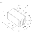
- FIG. 1 is a perspective view of a multilayer ceramic capacitor according to an embodiment of the present invention.
- FIG. 1 is a perspective view of a laminate according to an embodiment of the present invention.
- FIG. 2 is a perspective view of a main part of a capacitor according to an embodiment of the present invention.
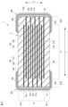
- FIG. 2 is a sectional view taken along the line II in FIG. 1; 2 is a sectional view taken along the line II-II in FIG. 1.
- FIG. (a) is a cross-sectional view taken along the line III--III in FIG. 2, and (b) is a view corresponding to the cross-sectional view taken along the line III--III in FIG. 2 in a conventional multilayer ceramic capacitor.
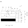
- FIG. 3 is a diagram corresponding to a cross-sectional view taken along line III-III in FIG. 2 in another embodiment of the present invention.
- 8 is a diagram showing region R in FIG. 7 in another embodiment of the present invention.
- FIG. FIG. 2 is a perspective view showing a part of the main part of a capacitor according to an embodiment of the present invention.
- FIG. 7 is a perspective view showing a part of the main part of a capacitor according to another embodiment of the present invention.
- FIG. 1 is a perspective view showing a multilayer ceramic capacitor 1 of this embodiment.
- the multilayer ceramic capacitor 1 includes a multilayer body 2 and an external electrode 20.
- the external electrode 20 includes a first external electrode 20a and a second external electrode 20b.
- FIGS. 1 to 7 an L direction, a W direction, and a T direction are shown.
- the L direction is the length direction L of the multilayer ceramic capacitor 1.
- the W direction is the width direction W of the multilayer ceramic capacitor 1.
- the T direction is the lamination direction T of the multilayer ceramic capacitor 1.
- the cross section shown in FIG. 4 is referred to as the LT cross section, and the cross section shown in FIG. 5 is referred to as the WT cross section.
- the length direction L, the width direction W, and the lamination direction T do not necessarily have to be perpendicular to each other.
- the length direction L, the width direction W, and the lamination direction T may intersect with each other.
- the laminate 2 has a substantially rectangular parallelepiped shape.
- the laminate 2 has two main surfaces M, two end surfaces E, and two side surfaces S.
- the main surface M is a surface facing the stacking direction T.
- the end surface E is a surface facing the length direction L.
- the side surface S is a surface facing in the width direction W.
- the two main surfaces M are referred to as a first main surface M1 and a second main surface M2.
- the two end faces E are referred to as a first end face E1 and a second end face E2.
- the two side surfaces S are referred to as a first side surface S1 and a second side surface S2.
- the corners of the laminate 2 are preferably rounded.
- a corner is a portion where at least two sides of the laminate 2 intersect.
- irregularities or the like may be formed on a part or all of the two main surfaces M, the two end surfaces E, and the two side surfaces S. Note that the size of the laminate 2 is not particularly limited.
- FIG. 2 is a perspective view of the laminate 2 according to the embodiment of the present invention.
- FIG. 3 is a perspective view of the capacitor main portion 3 according to the embodiment of the present invention.
- Laminated body 2 includes a capacitor main part 3 and two insulating parts 8. One of the two insulating parts 8 is a first insulating part 8a, and the other is a second insulating part 8b.
- the capacitor main portion 3 has a plurality of dielectric layers 4 and a plurality of internal electrode layers 10. The plurality of dielectric layers 4 and the plurality of internal electrode layers 10 are stacked on each other in the stacking direction T.
- the internal electrode layer 10 includes a first internal electrode layer 10a and a second internal electrode layer 10b. Details of the internal electrode layer 10 will be explained later.
- main portion side surfaces SS two surfaces facing each other in the width direction W are defined as main portion side surfaces SS.
- one of the two main-portion side surfaces SS is designated as a first main-portion side surface SS1
- the other is designated as a second main-portion side surface SS2.
- the laminate 2 is formed by disposing an insulating section 8 on each of the two main section side surfaces SS of the capacitor main section 3.
- the first insulating part 8a is arranged on the first main part side surface SS1
- the second insulating part 8b is arranged on the second main part side surface SS2.
- the insulating portion 8 is a member disposed on two main portion side surfaces SS of the capacitor main portion 3.
- the insulating section 8 has a sheet-like shape.
- the material constituting the insulating portion 8 is not particularly limited as long as it has insulating properties.
- the material constituting the insulating portion 8 may have the same main component as the material constituting the dielectric layer 4 .
- the material constituting the insulating portion 8 may be a resin component.
- the laminate 2 is configured such that the insulating parts 8 are arranged on the two main part side surfaces SS of the capacitor main part 3. Therefore, the end surface E of the laminate 2 is the same as the end surface E of the capacitor main portion 3. Similarly, the main surface M of the laminate 2 is the same as the main surface M of the capacitor main part 3.
- the side surface M of the laminate 2 becomes the surface of the insulating part 8 disposed on the main part side surface SS of the capacitor main part 3.
- the surface of the first insulating portion 8a that faces the first main portion side surface SS1 becomes the first side surface S1 of the stacked body 2.
- the surface of the second insulating portion 8b that faces the second main portion side surface SS2 becomes the second side surface S2 of the stacked body 2.
- the internal electrode layer 10 is exposed from the two main part side surfaces SS and the two end faces E of the capacitor main part 3. Specifically, the first internal electrode layer 10a is exposed from the first end surface E1 of the capacitor main section 3, and the second internal electrode layer 10b is exposed from the second end surface E2 of the capacitor main section 3. ing. Further, the first internal electrode layer 10a and the second internal electrode layer 10b are exposed from the first main part side surface SS1 and the second main part side surface SS2 of the capacitor main part 3. The first internal electrode layer 10a and the second internal electrode layer 10b exposed from the first main part side surface SS1 and the second main part side surface SS2 have a first insulating part on the first main part side surface SS1.
- the first internal electrode layer 10a and the second internal electrode layer 10b may not be exposed from the first main part side surface SS1 and the second main part side surface SS2. That is, the first internal electrode layer 10a and the second internal electrode layer 10b may be covered with the dielectric layer 4 at the first main part side surface SS1 and the second main part side surface SS2.
- the specific configuration of the capacitor main section 3 will be explained with reference to FIGS. 4 and 5.
- FIG. 4 is a sectional view taken along line II of the multilayer ceramic capacitor shown in FIG.
- the cross section of the portion of the laminate 2 shown in FIG. 4 is the LT cross section of the corresponding portion of the capacitor main portion 3.
- the laminate 2 includes a plurality of dielectric layers 4 and a plurality of internal electrode layers 10. The plurality of dielectric layers 4 and the plurality of internal electrode layers 10 are stacked on each other in the stacking direction T.
- the laminate 2 has an inner layer part IL and two outer layer parts OL in the lamination direction T.
- the outer layer portion OL includes a first outer layer portion OL1 and a second outer layer portion OL2.
- the first outer layer portion OL1 and the second outer layer portion OL2 are arranged to sandwich the inner layer portion IL.
- the inner layer portion IL includes a portion of the plurality of dielectric layers 4 and the plurality of internal electrode layers 10.
- a plurality of internal electrode layers 10 are arranged facing each other with the dielectric layer 4 interposed therebetween.
- the inner layer portion IL is a portion that forms a capacitance and substantially functions as a capacitor. From this, the inner layer part IL is also called an effective part.
- the first outer layer part OL1 is arranged on the first main surface M1 side of the laminate 2, and the second outer layer part OL2 is arranged on the second main surface M2 side of the laminate 2.
- the first outer layer portion OL1 is arranged between the internal electrode layer 10 closest to the first main surface M1 among the plurality of internal electrode layers 10 and the first main surface M1.
- the second outer layer portion OL2 is arranged between the internal electrode layer 10 closest to the second main surface M2 among the plurality of internal electrode layers 10 and the second main surface M2.
- the first outer layer portion OL1 and the second outer layer portion OL2 do not include the internal electrode layer 10, and the remaining dielectric layers 4 excluding the dielectric layer 4 for the inner layer portion IL among the plurality of dielectric layers 4 including.
- the first outer layer portion OL1 and the second outer layer portion OL2 function as a protective layer for the inner layer portion IL.
- the dielectric layer 4 includes an outer dielectric layer 5 and an inner dielectric layer 6.
- the outer dielectric layer 5 is the dielectric layer 4 that constitutes the first outer layer portion OL1 and the second outer layer portion OL2 among the dielectric layers 4.
- the outer dielectric layer 5 is arranged between the first main surface M1 and the internal electrode layer 10 closest to the first main surface M1, and between the second main surface M2 and the inner electrode layer 10 closest to the second main surface M2. It is located between the adjacent internal electrode layer 10.
- the inner dielectric layer 6 is the dielectric layer 4 that is located between the internal electrode layers 10 and forms the inner layer portion IL together with the internal electrode layers 10.
- the inner dielectric layer 6 is located between a first internal electrode layer 10a and a second internal electrode layer 10b, which will be described below.
- the number of dielectric layers 4 stacked on the laminate 2 can be, for example, 5 or more and 2000 or less.
- the number of dielectric layers 4 includes the number of outer dielectric layers 5 and the number of inner dielectric layers 6.
- a material for the dielectric layer 4 for example, a dielectric ceramic mainly composed of BaTiO 3 , CaTiO 3 , SrTiO 3 , CaZrO 3 or the like can be used. Further, a material obtained by adding subcomponents such as a Mn compound, a Fe compound, a Cr compound, a Co compound, or a Ni compound to these main components may also be used.
- the dielectric layer 4 can have a plurality of crystal grains containing a perovskite compound having a basic structure of BaTiO 3 .
- piezoelectric ceramic when used for the laminate 2, the laminate ceramic electronic component functions as a ceramic piezoelectric element.
- specific examples of piezoelectric ceramic materials include PZT (lead zirconate titanate) ceramic materials.
- the laminate ceramic electronic component functions as a thermistor element.
- semiconductor ceramic materials include, for example, spinel-based ceramic materials.
- the laminate ceramic electronic component functions as an inductor element. Furthermore, when the multilayer ceramic electronic component functions as an inductor element, the internal electrode layer becomes a coil-shaped conductor.
- magnetic ceramic materials include ferrite ceramic materials.
- the thickness of the dielectric layer 4 can be, for example, 0.3 um or more and 100 um or less. Furthermore, the number of outer dielectric layers 5 may be plural or one.
- the internal electrode layer 10 includes a first internal electrode layer 10a and a second internal electrode layer 10b.
- the first internal electrode layer 10a is the internal electrode layer 10 connected to the first external electrode 20a.
- the second internal electrode layer 10b is the internal electrode layer 10 connected to the second external electrode 20b.
- the external electrode 20 will be explained later.
- the first internal electrode layer 10a extends from the first end surface E1 toward the second end surface E2.
- the second internal electrode layer 10b extends from the second end surface E2 toward the first end surface E1.
- the first internal electrode layer 10a and the second internal electrode layer 10b each have a counter electrode section 11 and an extraction electrode section 12.
- the counter electrode portion 11 is a portion of the internal electrode layer 10 where the first internal electrode layer 10a and the second internal electrode layer 10b face each other in the stacking direction T.
- the extraction electrode portion 12 is a portion of the internal electrode layer 10 that is extracted from the counter electrode portion 11 to the end surface E1 or end surface E2 of the laminate 2.
- the counter electrode part 11 of the first internal electrode layer 10a is the first counter electrode part 11a
- the extraction electrode part 12 of the first internal electrode layer 10a is the first extraction electrode part 12a.
- the first extraction electrode portion 12a is a portion extracted from the first opposing electrode portion 11a to the first end surface E1 of the stacked body 2.
- the counter electrode portion 11 of the second internal electrode layer 10b is referred to as the second counter electrode portion 11b
- the extraction electrode portion 12 of the second internal electrode layer 10b is referred to as the second extraction electrode portion 12b.
- the second extraction electrode portion 12b is a portion extracted from the second opposing electrode portion 11b to the second end surface E2 of the stacked body 2.
- the number of internal electrode layers 10 can be, for example, 10 or more and 2000 or less.
- the number of internal electrode layers 10 includes the number of first internal electrode layers 10a and the number of second internal electrode layers 10b.
- the thickness of the internal electrode layer 10 can be, for example, 0.1 ⁇ m or more and 5.0 ⁇ m or less, preferably 0.2 ⁇ m or more and 2.0 ⁇ m or less.
- a plating film tends to grow when forming the metal layer of the external electrode 20 by plating. The metal layer will be explained later.
- the material of the internal electrode layer 10 can be, for example, metals such as Ni, Cu, Ag, Pd, and Au, alloys of Ni and Cu, alloys of Ag and Pd, and the like.
- the material of the internal electrode layer 10 may include dielectric particles having the same composition as the ceramic contained in the dielectric layer 4.
- the laminate 2 has an electrode facing portion LF and two end gap portions EG in the length direction L.
- the end gap portion EG has a first end gap portion EG1 and a second end gap portion EG2.
- the electrode facing portion LF is a portion where the first internal electrode layer 10a and the second internal electrode layer 10b face each other in the stacking direction T.
- the first opposing electrode portion 11a and the second opposing electrode portion 11b face each other in the stacking direction T.
- the electrode facing portion LF is located at the center of the laminate 2 in the longitudinal direction L.
- a capacitance is formed by the first counter electrode section 11a and the second counter electrode section 11b facing each other with the inner dielectric layer 6 interposed therebetween. Therefore, the electrode facing portion LF is also referred to as an effective portion.
- the end gap portion is a portion where the first internal electrode layer 10a and the second internal electrode layer 10b do not face each other in the stacking direction T. Specifically, in the stacking direction T, a portion where the first internal electrode layer 10a is disposed but where the second internal electrode layer 10b is not disposed is the first end gap portion EG1. Similarly, a portion where the second internal electrode layer 10b is placed but where the first internal electrode layer 10a is not placed is the second end gap portion EG2.
- the first end gap part EG1 corresponds to the part where the first extraction electrode part 12a is arranged
- the second end gap part EG2 corresponds to the part where the second extraction electrode part 12b is arranged. do.
- the first end gap portion EG1 functions as an extraction electrode to the first end surface E1 of the first internal electrode layer 10a
- the second end gap portion EG2 functions as a lead electrode to the first end surface E1 of the first internal electrode layer 10b. It functions as an extraction electrode to the end surface E2. Since the end gap portion EG is a division in the length direction L, it is also called an L gap.
- the length of the end gap portion EG in the longitudinal direction L can be, for example, 5 ⁇ m or more and 30 ⁇ m or less.
- the shape of the first opposing electrode portion 11a of the first internal electrode layer 10a is not particularly limited, but is preferably rectangular.
- the corner portions may be rounded, or the corner portions may be formed diagonally. That is, the corner portion may be tapered.
- the first counter electrode portion 11a may have a tapered shape that is inclined toward one of the edges.
- the shape of the second opposing electrode portion 11b of the second internal electrode layer 10b is not particularly limited, but is preferably rectangular.
- the corner portions may be rounded, or the corner portions may be formed diagonally. That is, the corner portion may be tapered.
- the second counter electrode portion 11b may have a tapered shape that is inclined toward one of the edges.
- the shape of the first extraction electrode portion 12a of the first internal electrode layer 10a is not particularly limited, but is preferably rectangular. However, the corner portions may be rounded, or the corner portions may be formed diagonally. That is, the corner portion may be tapered. Alternatively, the first extraction electrode portion 12a may have a tapered shape that is inclined toward one of the edges.
- the shape of the second extraction electrode portion 12b of the second internal electrode layer 10b is not particularly limited, but is preferably rectangular.
- the corner portions may be rounded, or the corner portions may be formed diagonally. That is, the corner portion may be tapered.
- the second extraction electrode portion 12b may have a tapered shape that is inclined toward one of the edges.
- the width of the first counter electrode part 11a of the first internal electrode layer 10a and the width of the first extraction electrode part 12a of the first internal electrode layer 10a may be formed to have the same width, or One side may be formed to have a narrow width.
- the width of the second counter electrode part 11b of the second internal electrode layer 10b and the width of the second extraction electrode part 12b of the second internal electrode layer 10b may be formed to have the same width, or One side may be formed to have a narrow width.
- the first extraction electrode portion 12a of the first internal electrode layer 10a may be curved toward the center of the first end surface E1 of the laminate 2.
- the second extraction electrode portion 12b of the second internal electrode layer 10b may be curved toward the center of the second end surface E2 of the laminate 2.
- the distance between the internal electrode layer 10 closest to the first main surface M1 of the internal electrode layer 10 drawn out to each end surface E and the internal electrode layer 10 closest to the second main surface M2 is the distance between the internal electrode layer 10 closest to the second main surface M2, The distance may be shorter than the distance between the opposing electrode section 11 on the main surface M1 side and the opposing electrode section 11 closest to the second main surface M2 side.
- the multilayer ceramic capacitor 1 of this embodiment a capacitance is formed by the opposing electrode parts 11 of the internal electrode layers 10 facing each other with the dielectric layer 4 interposed therebetween, and the characteristics of the capacitor are exhibited.
- the coverage of the LW surface of the internal electrode layer 10 is preferably 90% or more.
- the coverage of the LW plane is defined as the ratio of the remaining area after subtracting the area of the void from the area inside the edge of the internal electrode layer 10 when the internal electrode layer 10 is viewed from the LW plane. Ru.
- the higher the coverage of the LW surface the higher the capacitance of the capacitor. Note that when the coverage of the LW plane is low, the dielectric layers 4 are bonded to each other through gaps, so the bonding strength between the layers is increased, and delamination is less likely to occur.
- the thickness of the edge portion in the width direction W may be thicker than the thickness of the center portion in the width direction W.
- a step layer may be arranged in the L gap, that is, the end gap portion EG.
- the step layer is a dielectric layer 4 that is additionally disposed in the end gap part EG in order to reduce the difference in length in the stacking direction T between the end gap part EG and the electrode facing part LF.
- the step layer may be arranged such that the internal electrode layer 10 partially covers the step layer. Or, on the contrary, the step layer may be arranged to cover a part of the internal electrode layer 10.
- the step layer has the same thickness as the internal electrode layer 10.
- the step layer has the same components as the dielectric layer 4.
- the components of the dielectric layer 4 are not limited to these.
- a dummy electrode layer may be placed in the L gap.
- the dummy electrode layer can be arranged in at least one of the inner layer part IL and the outer layer part OL.
- the outer layer portion OL includes a first outer layer portion OL1 and a second outer layer portion OL2.
- the dummy electrode layer is preferably arranged on a portion corresponding to a location where the L gap is translated in the stacking direction T. That is, the dummy electrode layer is preferably arranged at a position corresponding to the L gap in the length direction L of the outer layer portion OL.
- the dummy electrode layer can include a first dummy electrode layer and a second dummy electrode layer.
- the first dummy electrode layer preferably has a thickness similar to the total thickness of the first internal electrode layers 10a. In other words, the thickness of the first dummy electrode layer is preferably equal to the thickness of the first internal electrode layer 10a x the number of first internal electrode layers 10a.
- the first dummy electrode layer may be one or more than one, as long as it has the same thickness as the total thickness of the first internal electrode layers 10a.
- the second dummy electrode layer is also similar to the first dummy electrode layer. That is, the second dummy electrode layer preferably has a thickness similar to the total thickness of the second internal electrode layers 10b. In other words, the second dummy electrode layer preferably has a thickness equal to the thickness of the second internal electrode layer 10b x the number of second internal electrode layers 10b.
- the second dummy electrode layer may be one or more than one, as long as it has the same thickness as the total thickness of the second internal electrode layers 10b.
- the external electrode 20 includes a first external electrode 20a and a second external electrode 20b.
- the first external electrode 20a is an external electrode 20 disposed on the first end surface E1 of the stacked body 2.
- the first external electrode 20a is electrically connected to the first internal electrode layer 10a.
- the second external electrode 20b is the external electrode 20 disposed on the second end surface E2 of the stacked body 2.
- the second external electrode 20b is electrically connected to the second internal electrode layer 10b.
- the external electrode 20 extends from the end surface E to part of the two main faces M and to part of the two side faces S.
- a portion of the external electrode 20 disposed on the end surface E is referred to as an end surface external electrode 25.
- a portion of the external electrode 20 disposed on a part of the main surface M is referred to as a main surface external electrode 26 .
- a portion of the external electrode 20 disposed on a part of the side surface S is referred to as a side surface external electrode 27 .
- the portion of the first external electrode 20a disposed on the first end surface E1 is the first end surface external electrode 25a.
- a portion of the first external electrode 20a that is disposed on a part of the first main surface M1 or a part of the second main surface M2 is referred to as a first main surface external electrode 26a.
- a portion disposed on a portion of the first side surface S1 or a portion of the second side surface S2 is referred to as a first side surface external electrode 27a.
- the portion of the second external electrode 20b disposed on the second end surface E2 is the second end surface external electrode 25b.
- a portion of the second external electrode 20b that is disposed on a part of the first main surface M1 or a part of the second main surface M2 is defined as a second main surface external electrode 26b.
- a portion of the second external electrode 20b that is disposed on a portion of the first side surface S1 or a portion of the second side surface S2 is referred to as a second side surface external electrode 27b.
- the layer structure of the external electrode 20 will be explained based on FIGS. 4 and 5.
- the external electrode 20 includes three layers: a base electrode layer 21 , an inner plating layer 23 , and a surface plating layer 24 . These layers are arranged in this order from the end surface E of the laminate 2: base electrode layer 21, inner plating layer 23, and surface plating layer 24.
- the first external electrode 20a includes a first base electrode layer 21a, a first inner plating layer 23a, and a first surface plating layer 24a.
- the second external electrode 20b includes a second base electrode layer 21b, a second inner plating layer 23b, and a second surface plating layer 24b.
- the first base electrode layer 21a is disposed on the first end surface E1 of the laminate 2, and covers the first end surface E1.
- the first base electrode layer 21a extends from the first end surface E1 to a part of the first main surface M1, a part of the second main surface M2, a part of the first side surface S1, and a second side surface S2. It may extend to a part of the
- the second base electrode layer 21b is arranged on the second end surface E2 of the laminate 2, and covers the second end surface E2.
- the second base electrode layer 21b extends from the second end surface E2 to a part of the first main surface M1, a part of the second main surface M2, a part of the first side surface S1, and a second side surface S2. It may extend to a part of the
- the first base electrode layer 21a and the second base electrode layer 21b include at least one selected from a baked layer, a conductive resin layer, a thin film layer, a direct plating layer, and the like.
- the baking layer contains a glass component and a metal.
- the glass component includes at least one selected from B, Si, Ba, Mg, Al, Li, and the like.
- the metal includes, for example, at least one selected from Cu, Ni, Ag, Pd, Ag-Pd alloy, Au, and the like.
- the baking layer may have multiple layers. The baked layer is obtained by applying a conductive paste containing a glass component and a metal to the laminate 2, and then baking it. This baking, that is, firing, may be performed simultaneously with the firing of the internal electrode layer 10, or may be performed separately after the internal electrode layer 10 is fired.
- the thickness is preferably, for example, 0.1 ⁇ m or more and 200 ⁇ m or less.
- the longitudinal direction of the base electrode layer 21 on each surface is The thickness of the baked layer at the center is preferably, for example, 0.1 ⁇ m or more and 200 ⁇ m or less.
- the conductive resin layer contains a thermosetting resin and a metal.
- the conductive resin layer contains thermosetting resin. Therefore, it is more flexible than, for example, a conductive layer made of a plated film or a fired product of conductive paste. Therefore, even if a ceramic electronic component such as the multilayer ceramic capacitor 1 is subjected to physical shock or shock due to thermal cycles, the conductive resin layer functions as a buffer layer and prevents cracks in the capacitor. be able to.
- the metal contained in the conductive resin layer Ag, Cu, or an alloy thereof can be used. Further, as the metal, metal powder whose surface is coated with Ag can be used. When using a metal powder whose surface is coated with Ag, it is preferable to use Cu or Ni as the metal powder. Further, as the metal, Cu which has been subjected to oxidation prevention treatment can also be used.
- the reason for using Ag conductive metal powder as a conductive metal is that Ag has the lowest specific resistance among metals, making it suitable for electrode materials, and since Ag is a noble metal, it does not oxidize and has high resistance. It's for a reason. Note that the reason for using Ag-coated metal is that it is possible to reduce the amount of Ag used while making the most of the above characteristics of Ag, and to make the base metal cheaper.
- the metal is contained in an amount of 35 vol% or more and 75 vol% or less based on the volume of the entire conductive resin.
- the shape of the metal contained in the conductive resin layer is not particularly limited.
- the shape of the metal in other words, the shape of the conductive filler may be spherical or flat.
- the average particle size of the metal contained in the conductive resin layer is not particularly limited.
- the average particle size of the metal, for example, the conductive filler can be, for example, about 0.3 ⁇ m or more and 10 ⁇ m or less.
- the metal contained in the conductive resin layer is mainly responsible for the conductivity of the conductive resin layer. Specifically, when the conductive fillers come into contact with each other, a current-carrying path is formed inside the conductive resin layer.
- the metal contained in the conductive resin layer can be spherical or flat, but it is preferable to use a mixture of spherical metal powder and flat metal powder.
- thermosetting resins such as epoxy resin, phenol resin, urethane resin, silicone resin, and polyimide resin can be used.
- epoxy resin is one of the most suitable resins because of its excellent heat resistance, moisture resistance, and adhesion.
- the resin contained in the conductive resin layer is contained in an amount of 25 vol% or more and 65 vol% or less with respect to the total volume of the conductive resin.
- the conductive resin layer contains a curing agent together with the thermosetting resin.
- the curing agent when an epoxy resin is used as the base resin, various known compounds such as phenol, amine, acid anhydride, and imidazole compounds can be used as the curing agent for the epoxy resin.
- the conductive resin layer may be placed on the baking layer so as to cover the baking layer, or may be placed directly on the laminate 2. Further, the conductive resin layer may have multiple layers.
- the thickness of the conductive resin layer is preferably about 10 ⁇ m or more and 200 ⁇ m or less, for example.
- the length of the base electrode layer 21 on each surface is preferably, for example, 5 ⁇ m or more and 50 ⁇ m or less.
- the thin film layer is formed by a thin film forming method such as a sputtering method or a vapor deposition method, and the metal particles are deposited. It can be made into a layer with a thickness of 1 ⁇ m or less.
- the external electrode 20 may include a direct plating layer.
- the direct plating layer is a plating layer directly formed on the surface of the laminate 2. That is, the multilayer ceramic capacitor 1 may have a structure including a direct plating layer electrically connected to the first internal electrode layer 10a or the second internal electrode layer 10b. In the case of directly forming the plating layer, the plating layer may be formed directly after disposing a catalyst on the surface of the laminate 2 as a pretreatment.
- the direct plating layer preferably contains at least one metal selected from, for example, Cu, Ni, Sn, Pb, Au, Ag, Pd, Bi, or Zn, or an alloy containing the metal.
- the direct plating layer is preferably formed using Cu, which has good bonding properties with Ni.
- the thickness of each directly plated layer is preferably 1.0 ⁇ m or more and 15 ⁇ m or less. Moreover, it is preferable that the plating layer does not contain glass.
- the metal ratio per unit volume of the plating layer is preferably 99% by volume or more.
- the plating layer on the base electrode layer 21 may be one layer or multiple layers.
- the plating layer is two-layered, it is preferable to order the Ni plating layer and the Sn plating layer from the bottom layer.
- the plating layer is made into three layers, it is preferable to set it as a Sn plating layer, a Ni plating layer, and a Sn plating layer from the bottom.
- a two-layer structure of Ni plating and Sn plating is preferred. In the following, a case where the plating layer is two layers, the inner plating layer 23 and the front plating layer 24, will be explained.
- the inner plating layer 23 is disposed on the base electrode layer 21 and covers at least a portion of the base electrode layer 21.
- the surface plating layer 24 is disposed on the inner plating layer 23 and covers at least a portion of the inner plating layer 23.
- the plating layers including the inner plating layer 23 and the surface plating layer 24, are made of at least one selected from metals such as Cu, Ni, Ag, Pd, Au and Sn, and alloys such as Ag-Pd alloy. It is preferable to include.
- the inner plating layer 23 is preferably a Ni plating layer
- the surface plating layer 24 is preferably a Sn plating layer.
- the Ni plating layer can prevent the base electrode layer from being eroded by solder when mounting the ceramic electronic component.
- the Sn plating layer improves the wettability of solder when mounting ceramic electronic components, and can facilitate mounting.
- the thickness of each plating layer is preferably 1.0 ⁇ m or more and 15 ⁇ m or less.
- FIG. 5 is a sectional view taken along the line II-II of the multilayer ceramic capacitor shown in FIG.
- the laminate 2 has, in the width direction W, an electrode facing part WF where the internal electrode layer 10 faces, and a side gap part SG.
- the side gap portion SG includes a first side gap portion SG1 and a second side gap portion SG2.
- the first side gap portion SG1 and the second side gap portion SG2 are arranged to sandwich the electrode facing portion WF.
- the first side gap portion SG1 is located between the electrode facing portion WF and the first side surface S1
- the second side gap portion SG2 is located between the electrode facing portion WF and the second side surface S2. do.
- the first side gap portion SG1 is located between the end of the internal electrode layer 10 on the first side surface S1 side and the first side surface S1
- the second side gap portion SG2 is located between the inner electrode layer 10 and the first side surface S1. It is located between the end of the electrode layer 10 on the second side surface S2 and the second side surface S2.
- the first side gap portion SG1 and the second side gap portion SG2 do not include the internal electrode layer 10 but only include the dielectric layer 4.
- the first side gap portion SG1 and the second side gap portion SG2 function as a protective layer for the internal electrode layer 10. Since the side gap portion SG is a division in the width direction W, it is also called a W gap.
- the length of the side gap portion SG in the width direction W can be, for example, 5 ⁇ m or more and 50 ⁇ m or less.
- the size of the multilayer ceramic capacitor 1 is not particularly limited.
- the size of the multilayer ceramic capacitor 1 can be set as follows, for example. That is, the dimension in the length direction L of the multilayer ceramic capacitor 1 including the laminate 2 and the external electrode 20 is defined as the L dimension.
- the L dimension is preferably 0.2 mm or more and 6.5 mm or less.
- the dimension of the multilayer ceramic capacitor 1 including the multilayer body 2 and the external electrode 20 in the stacking direction T is defined as the T dimension.
- the T dimension is preferably 0.1 mm or more and 6.5 mm or less.
- the dimension in the width direction W of the multilayer ceramic capacitor 1 including the laminate 2 and the external electrode 20 is defined as the W dimension.
- the W dimension is preferably 0.1 mm or more and 5.5 mm or less. Note that the length of each part of the laminate 2 and the external electrode 20 can be measured with a micrometer or an optical microscope.
- the multilayer ceramic capacitor 1 is a two-terminal capacitor.
- the multilayer ceramic capacitor 1 of this embodiment is characterized by the corner portions of the capacitor main portion 3. This will be explained based on FIGS. 6 and 7.
- 6(a) is a cross-sectional view taken along the line III-III in FIG. 2
- FIG. 6(b) is a view corresponding to the cross-sectional view taken along the line III-III in FIG. 2 in a conventional multilayer ceramic capacitor.
- FIG. 7 is a diagram corresponding to a sectional view taken along line III-III in FIG. 2 in another embodiment of the present invention.
- a corner C which is a portion where the main surface M and the main portion side surface SS intersect, is curved.
- the insulating portion 8 covers the corner C.
- the corner where the first main surface M1 and the first main part side surface SS1 intersect is the corner C1
- the corner where the second main surface M2 and the first main part side surface SS1 intersect. is the corner C2.
- the corner where the first main surface M1 and the second main section side surface SS2 intersect is defined as a corner section C3, and the second main surface M2 and the second main section side surface SS2 intersect. The corner where they intersect is called corner C4.
- the corner C is curved. As shown in FIG. 6(b), in the conventional multilayer ceramic capacitor 1, the corner C is bent at a substantially right angle when viewed from the length direction L of the capacitor main portion 3, in other words, in the WT cross section. .
- the corner C is curved, as shown in FIG. 6(a).
- the corner C1 is curved across the first main surface M1 and the first main portion side surface SS1.
- the corner C2 is curved across the second main surface M2 and the first main portion side surface SS1.
- the corner portion C3 is curved across the first main surface M1 and the second main portion side surface SS2.
- the corner C4 is curved across the second main surface M2 and the second main portion side surface SS2.
- the insulating portion 8 covers this curved corner C. That is, as shown in FIG. 6A, the insulating portion 8 covers the corner C when viewed from the length direction L of the capacitor main portion 3, in other words, in the WT cross section.
- the second corner C2 will be explained as an example.
- the outer edge of the second corner C2 does not pass through a point P3, which is a point where the second main surface M2 and the first main portion side surface SS1 intersect. This is because the second corner C2 is curved due to the absence of the outer dielectric layer 5 near the point P3.
- a point on the first main surface M1 side of the point P3 on the first main part side surface SS1 is defined as a point P2. Further, a point on the second main surface M2 that is closer to the second main portion side surface SS2 than the point P3 is referred to as a point P4.
- the second corner C2 is curved to connect the point P2 and the point P4 with a curved line.
- the first insulating portion 8a is also arranged in a portion surrounded by points P2, P3, and P4. Thereby, the second corner C2 is covered by the first insulating portion 8a from point P2 to point P4.
- first insulating part 8a covers the first corner C1 and the second corner C2
- second insulating part 8b covers the third corner C3 and the fourth corner C4. Covered.
- the insulating portion 8 continuously covers the corner C when the capacitor main portion 3 is viewed from the length direction L thereof.
- the insulating portion 8 starts from an end point on the main side surface SS of the corner C, and continuously covers the corner C from the starting point.
- the second corner C2 will be explained as an example. As shown in FIG. 6(a), at the second corner C2, the first insulating section 8a continues from point P2 to point P4 without separating from the capacitor main section 3. Covers C2.
- the point P2 is the end point of the second corner C2 above the first main part side surface SS1. Therefore, it can be said that the first insulating portion 8a continuously covers the second corner C2 from the first main portion side surface SS1 when the laminate 2 is viewed from the length direction L thereof. The same applies to corners C other than the second corner C2.
- the first insulating part 8a continuously covers the first corner C1 and the second corner C2, and similarly , the second insulating portion 8b, the third corner C3, and the fourth corner C4 are continuously covered.
- the insulating part 8 is extended from the upper end point of the main part side surface SS of the corner part C along the shape of the corner part C to the 50th corner of the corner part C. % or more.
- the second corner C2 will be explained as an example. As shown in FIG. 6(a), at the second corner C2, the first insulating section 8a continues from point P2 to point P4 without separating from the capacitor main section 3. Covers C2. Point P2 is the end point of the second corner C2 above the first main portion side surface SS1.
- the first insulating portion 8a moves the second corner C2 from the point P2, which is the upper end point of the first main portion side surface SS1, to the second corner C2. 50% or more of the second corner C2 is covered along the shape of the corner C2. The same applies to corners C other than the second corner C2.
- the first insulating part 8a is located above the first main part side surface SS1 of the first corner C1 and the second corner C2. From the end point, cover 50% or more of the first corner C1 and the second corner C2 along the shapes of the first corner C1 and the second corner C2, and similarly cover the second corner C1 and the second corner C2.
- the insulating portion 8b extends from the end points of the third corner C3 and the fourth corner C4 above the second main part side surface SS2 along the shapes of the third corner C3 and the fourth corner C4. , covering 50% or more of the third corner C3 and the fourth corner C4.
- the roughness of the corner C is greater than the roughness of the insulating portion 8 located above the corner C.
- the roughness of the corner C is greater than the roughness of the corner of the laminate 2 corresponding to the corner C. This will be explained below.
- first outer corner K1 the corner where the first main surface M1 and the first side surface S1 intersect is referred to as a first outer corner K1.
- second outer corner K2 the corner where the second main surface M2 and the first side surface S1 intersect is defined as a second outer corner K2.
- the corner where the first main surface M1 and the second side surface S2 intersect is defined as a third outer corner K3.
- the corner where the second main surface M2 and the second side surface S2 intersect is defined as a third outer corner K4.
- the first side surface S1 is the surface of the first insulating portion 8a that faces the surface that is in contact with the first main portion side surface SS1.
- the second side surface S2 is a surface of the second insulating portion 8b that faces the surface that is in contact with the second main portion side surface SS2.
- the roughness of the first corner C1 is greater than the roughness of the first outer corner K1.
- the roughness of the second corner C2 is greater than the roughness of the second outer corner K2
- the roughness of the third corner C3 is greater than the roughness of the third outer corner K3.
- the roughness of the fourth corner C4 is greater than the roughness of the fourth outer corner K4.
- the adhesion force between the capacitor main part 3 and the insulating part 8 can be increased due to the anchor effect due to the surface shape of the corner C. Thereby, the occurrence of peeling can be prevented or suppressed.
- the roughness of the corner C is preferably 0.05 um or more and less than 1.00 um.
- the roughness is less than 0.05 um, the anchoring effect tends to be insufficient.
- the roughness is 1.00 um or more, the surface unevenness becomes too large, so that the capacitor main part 3 and the insulating part 8 cannot be sufficiently adhered to each other, and air entrapment or peeling may occur.
- Surface roughness can be measured as follows. That is, a 1/2WT plane cross section of the laminate 2 is observed using a SEM. Then, the laminated body 2 and the insulating part 8 are binarized, and the roughness of the corner C of the capacitor main part 3 and the outer corner K of the laminated body 2 is measured. Note that the outer corner K of the laminate 2 and the outer corner K of the insulating section 8 have the same meaning and indicate the same position. More specifically, the roughness was measured using image analysis software using a Keyence digital microscope based on the contour lines of the corner C of the capacitor main part 3 and the outer corner K of the laminate 2. did. The roughness measured by this image analysis software is surface roughness Sa in accordance with the ISO-25178 standard.
- FIG. 7 is a diagram corresponding to a sectional view taken along line III-III in FIG. 2 in another embodiment of the present invention.
- the corner C is provided with a convex portion V that protrudes in the width direction W.
- a first convex portion V1 that protrudes in the direction of the first insulating portion 8a is arranged at the corner C1
- a third convex portion V3 that protrudes in the direction of the second insulating portion 8b is arranged at the corner C3.
- a second convex portion V2 protruding in the direction of the first insulating portion 8a is disposed at the corner C2
- a second convex portion V2 protruding toward the first insulating portion 8a is disposed at the corner C4.
- a fourth convex portion V4 is arranged to protrude in the direction of the insulating portion 8b.
- the second corner C2 will be explained as an example.
- the apex of the second convex portion V2 in the direction of the first insulating portion 8a is indicated by a point P5.
- a point P5 which is the apex of the second convex portion V2, protrudes from the first main part side surface SS1 of the capacitor main part 3 toward the first side surface S1 of the laminate 2. .
- the length D5 by which the point P5, which is the apex of the second convex portion V2, protrudes from the first main side surface SS1 of the capacitor main portion 3 in the direction of the first side surface S1 of the laminate 2 is, for example, 0.5 ⁇ m.
- the thickness can be set to 10.0 ⁇ m or more.
- the thickness of the second outer layer portion OL2 in the stacking direction T is indicated by D1.
- the point P5, which is the apex of the second convex portion V2 is located in the range from the line L1 to the line L2 in the stacking direction T in the second outer layer portion OL2. That is, the point P5, which is the apex of the second convex portion V2, is located at a position with a length of 10% or more and 60% or less of the thickness of the second outer layer portion OL2 in the stacking direction T from the second main surface M2. ing.
- the arrangement of the second convex portion V2 is the same for convex portions V other than the second convex portion V2.
- the convex portion V is located at a position at a length of 10% or more and 60% or less from the first main surface M1 or the second main surface M2 of the thickness in the stacking direction T of the laminate 2 of the outer layer portion OL. It is located in Note that the position of the convex portion V is the position of the apex of the convex portion V in the width direction W.
- FIG. 8 is a diagram showing a convex portion V of another form.
- FIG. 8 is a diagram corresponding to region R in FIGS. 8 and 7.
- a flat portion V4F is provided between the convex portion V4 and the inner layer portion IL in the stacking direction T.
- This flat portion V4F is a straight portion on the edge surface of the outer dielectric layer 5 that is parallel to the second main portion side surface SS2.
- the adhesion between the capacitor main portion 3 and the second insulating portion 8b at the boundary between the second outer layer portion OL2 and the inner layer portion IL is determined on the second main portion side surface SS2. It becomes easier to improve. This further suppresses delamination between the second outer layer part OL2 and the inner layer part IL and moisture etc. from entering between the second outer layer part OL2 and the inner layer part IL. I can do it.
- FIG. 9 is a perspective view showing a part of the capacitor main section 3.
- FIG. 10 is a perspective view showing a part of the capacitor main part 3 of another form. More specifically, FIGS. 9 and 10 show a part of the capacitor main part 3 up to a part of the length in the length direction L of the capacitor main part 3 included in the region R in FIG. FIG.
- the convex portion V shown in FIG. 9 and the convex portion V shown in FIG. 10 differ in the value of D5, which is the height of the convex portion V, in the length direction L.
- the height D5 of the convex portion V shown in FIG. 9 is constant in the length direction L. That is, the convex portions V are formed continuously in the length direction L.
- the convex portions V do not need to be formed continuously in the length direction L as shown in FIG.
- the height D5 of the convex portion V in the length direction L it is also possible to create a configuration in which a plurality of peaks are present. That is, the convex portions V can be made non-uniform or discontinuous in the length direction L. Also, in the discontinuous form, the peaks may be arranged at regular intervals or at irregular intervals.
- FIG. 10 shows an example of a configuration in which multiple mountains exist.
- Point P5 in FIG. 10 indicates the point where D5 is maximum in the length direction L. That is, point P5 indicates the position of the top of the mountain.
- point B1 in FIG. 10 indicates the point where D5 is the minimum in the length direction L. That is, point B1 indicates the position of the valley between the peaks.
- the convex portion V can be formed such that point P5 and point B1 repeat multiple times in the length direction L. Thereby, it is possible to realize a convex portion V having a plurality of peaks in the length direction L.
- the convex portion V is not in contact with either the first internal electrode layer 10a or the second internal electrode layer 10b.
- the second convex portion V2 will be explained as an example.
- a point P1 indicates the boundary between the first outer layer portion OL1 and the inner layer portion IL on the first main portion side surface SS1.
- the second convex portion V2 does not extend beyond the point P1 and within the range of the inner layer portion IL. Therefore, the second convex portion V2 is not in contact with either the first internal electrode layer 10a or the second internal electrode layer 10b.
- the convex portion V is not in contact with either the first internal electrode layer 10a or the second internal electrode layer 10b. In other words, the convex portion V is not joined to the internal electrode layer 10.
- the protrusion V can be a protrusion different from the protrusion due to roughness on the corner C. That is, the unevenness of the corner C can be a discontinuous convexity.
- the convex portion V may be a convex portion that is continuous with the concave and convex portions of the corner portion C. That is, the protrusion V can be a protrusion extending from the corner C.
- the width of the protrusion of the convex portion V is wider than the width of the protrusion related to the roughness of the corner portion C.
- the width of the protrusion and convexity means the width in the WT cross section.
- the main component of the material forming the convex portions V be the same as that of the dielectric layer 4.
- the convex portions V By arranging the convex portions V as described above, when moisture enters from the interface between the laminate 2 and the insulating portion 8, the convex portions V can prevent moisture from entering the effective portion.
- the insulating section will be explained below.
- the thickness of the insulating portion 8 is preferably 10 um or more and 50 um or less. If the thickness of the insulating part 8 is less than 10 um, it will not be possible to sufficiently cover the interface exposed on the main part side surface SS of the capacitor main part 3. Therefore, moisture resistance reliability may decrease. On the other hand, if the thickness of the insulating portion 8 is 50 um or more, the dimensions of the laminate 2 will become too large. Therefore, the degree of freedom in mounting the multilayer ceramic capacitor 1 is reduced.
- the insulating section 8 may have one layer or two layers.
- the total thickness of the two layers may be 10 um or more and 50 um or less, or the thickness of each layer may be 10 um or more and 50 um or less.
- first to fourth corners C were explained as being uniform.
- the first to fourth corners C are not uniform, and for example, the above-mentioned shapes can be made different for each corner C.
- ⁇ Preparation of laminated block> Prepare conductive paste for dielectric sheets and internal electrode layers.
- the conductive paste for the dielectric sheet and internal electrode layer contains a binder and a solvent. Known organic binders and organic solvents can be used as the binder and solvent.
- a conductive paste for the internal electrode layer is printed in a predetermined pattern on the dielectric sheet by, for example, screen printing or gravure printing to form a pattern for the internal electrode layer.
- a predetermined number of dielectric sheets for the outer layer on which the internal electrode layer pattern is not printed are laminated, then dielectric sheets on which the internal electrode layer pattern is printed are laminated one after another, and then the other dielectric sheet for the outer layer is layered on top of that.
- a predetermined number of dielectric sheets are laminated to produce a laminated sheet. The laminated sheet is pressed in the lamination direction by means such as a hydrostatic press to produce a laminated block.
- ⁇ Preparation of laminated chip> Cut the laminated block to a specified size and cut out the laminated chip.
- the laminated chip becomes the capacitor main part 3 by firing.
- the capacitor main part 3 before firing may be referred to as a capacitor main part precursor.
- the corners of the laminated chips are rounded by barrel polishing. At that time, by changing the barrel polishing time, rotation speed, or both, a convex portion is formed around the corner.
- the surfaces of the corners can be roughened by sandpapering, sandblasting, etc. so that the corners have a desired roughness.
- the surface of the corner can be made rougher by using sandpaper with a coarser roughness.
- the desired roughness can be achieved by changing the amount of sandpaper applied.
- the desired roughness can be achieved by controlling the intensity and/or duration of the blasting. Note that the method for roughening the corners so that they have the desired roughness is not limited to the above-mentioned method, and various methods can be used.
- the convex portion V when rounding the corners of the laminated chip, for example, by changing the amount of pressing of the sandpaper, it is possible to form the convex portion V in a desired shape.
- the method for forming the convex portions V is not limited to this.
- the convex portions V can also be formed by depositing the scraped material.
- insulating parts 8 are formed on the two main part side surfaces SS of the precursor of the capacitor main part 3 having a predetermined corner shape.
- the insulating portion 8 may be formed by punching an insulating sheet onto the side surface SS of the main portion, or may be formed on the side surface SS of the main portion using a dip method.
- the elastic body used for punching has the desired hardness and the amount of pushing is adjusted so that the insulating part 8 can be formed from the side surface SS of the main part. It can be formed to cover any corner part.
- the insulating part 8 When forming the insulating part 8 by the Dipping method, the insulating part can be formed into a desired shape by changing the amount of pressing during dipping, the amount of insulating paste, or both.
- the laminated chips are fired to produce a laminated body 2.
- the firing temperature depends on the materials of the dielectric layer 4 and the internal electrode layer 10, it is preferably 900° C. or more and 1400° C. or less.
- the insulating part 8 may be formed after the laminated chip is fired, or the insulating part 8 may be formed before firing, and the laminated chip provided with the insulating part 8 may be fired.
- the outer corner K of the laminate 2 in other words, the outer corner K of the insulating part 8, before or after the above-described firing. Further, in this case, the outer corner K can also be roughened to a predetermined roughness.
- the method for rounding and roughening the surface can be the same as the method for processing the corners of the laminated chip described above.
- ⁇ External electrode> Formation of the external electrode 20 will be explained.
- a conductive paste that will become the base electrode layer 21 is applied to both end faces E of the laminate 2 to form the base electrode layer 21.
- a conductive paste containing a glass component and a metal is applied, for example, by a method such as dipping, and then a baking process is performed to form the base electrode layer 21.
- the temperature of the baking treatment at that time is preferably 700°C or more and 900°C or less. Thereafter, if necessary, the surface of the baked layer is plated.
- the conductive resin layer can be formed by the following method.
- the conductive resin layer may be formed on the surface of the baked layer, or the conductive resin layer alone may be directly formed on the laminate 2 without forming the baked layer.
- a conductive resin paste containing a thermosetting resin and a metal component is applied onto the baking layer or the laminate 2, and heat treatment is performed at a temperature of 250° C. or higher and 550° C. or lower.
- the resin is thermoset to form a conductive resin layer.
- the atmosphere during the heat treatment at this time is preferably a N 2 atmosphere. Further, in order to prevent resin scattering and oxidation of various metal components, it is preferable to suppress the oxygen concentration to 100 ppm or less.
- the base electrode layer 21 can be formed by a thin film forming method such as a sputtering method or a vapor deposition method.
- the base electrode layer 21 formed of a thin film layer is a layer with a thickness of 1 ⁇ m or less on which metal particles are deposited.
- a plating layer may be provided directly on the exposed portion of the internal electrode layer 10 of the laminate 2.
- it can be formed by the following method. That is, plating is performed on the first end surface E1 and the second end surface E2 of the laminate 2, and a plating film is formed directly on the exposed portion of the internal electrode layer 10.
- electrolytic plating requires pretreatment with a catalyst or the like in order to improve the plating deposition rate, which has the disadvantage of complicating the process. Therefore, it is usually preferable to employ electrolytic plating.
- As the plating method it is preferable to use barrel plating.
- an upper layer plating electrode which is normally formed on the surface of the lower layer plating electrode, may be formed in the same manner.
- a plating layer is formed on the surface of the base electrode layer, the surface of the conductive resin layer, or the surface of the direct plating layer.
- a Ni plating layer and a Sn plating layer were formed on the baked layer.
- the Ni plating layer and the Sn plating layer are sequentially formed by, for example, a barrel plating method. In this way, a multilayer ceramic capacitor 1 is obtained.
- the method for forming the external electrode 20 is not limited to the method described above.
- Ni is screen printed on the two end faces E of the laminate 2. Thereafter, the two end faces E are dipped in Cu to form a Cu layer on the Ni. After that, Ni and Sn plating may be performed to form the external electrodes 20.
- the explanation was centered on the portion where the two surfaces of the laminate 2 or the capacitor main portion 3 intersect.
- the fact that the corner is curved and that the corner has a predetermined roughness is not limited to the corner where two surfaces intersect.
- the portion where the three surfaces of the laminate 2 or the capacitor main portion 3 intersect can be similarly curved, the surface roughened, or both.
- ⁇ 1> including a plurality of stacked dielectric layers; A first main surface and a second main surface facing each other in the stacking direction; a first main part side surface and a second main part side surface facing each other in the width direction perpendicular to the lamination direction; a first end face and a second end face facing each other in a length direction perpendicular to the lamination direction and the width direction; a first internal electrode layer stacked alternately with the plurality of dielectric layers and exposed on the first end surface, the first main part side surface, and the second main part side surface; a capacitor main part including a second internal electrode layer stacked alternately with the plurality of dielectric layers and exposed on the second end face, the first main part side surface, and the second main part side surface; a first insulating portion disposed on a side surface of a first main portion of the capacitor main portion; a second insulating portion disposed on a side surface of a second main portion of the capacitor main portion; a first external electrode provided so as to extend from the first end
- the first insulating part covers the first corner and the second corner, The second insulating part covers the third corner and the fourth corner, A surface of the first insulating portion that faces a surface in contact with a side surface of the first main portion is a first side surface of the laminate; A surface of the second insulating section that faces a surface in contact with a side surface of the second main portion is a second side surface of the laminate;
- the first insulating section includes a first outer corner where the first main surface and the first side surface intersect, and a second outer corner where the second main surface and the first side surface intersect.
- the second insulating section includes a third outer corner where the first main surface and the second side surface intersect, and a fourth outer corner where the second main surface and the second side surface intersect. has a corner,
- the roughness of the first corner is greater than the roughness of the first outer corner
- the roughness of the second corner is greater than the roughness of the second outer corner
- the roughness of the third corner is greater than the roughness of the third outer corner
- the roughness of the fourth corner is greater than the roughness of the fourth outer corner.
- the surface roughness of the first corner, the second corner, the third corner, and the fourth corner is 0.05 um or more and 1.00 um or less,
- the main part of the capacitor is an inner layer portion in which the first internal electrode layer, the dielectric layer, and the second internal electrode layer are alternately laminated; a first outer layer portion made of the dielectric layer and located on the first main surface side of the inner layer portion in the lamination direction; a second outer layer portion that is located on the second main surface side of the inner layer portion in the lamination direction and is made of the dielectric layer; Projects in the direction of the first insulating part from the first main surface of the first outer layer part at a position that is 10% or more and 60% or less of the thickness of the first outer layer part in the lamination direction.
- a third protrusion protruding in the direction of the first protrusion and the second insulating part is arranged, Projects in the direction of the first insulating part from the second main surface of the second outer layer part at a position that is 10% or more and 60% or less of the thickness of the second outer layer part in the lamination direction. a second convex portion and a fourth convex portion protruding in the direction of the second insulating portion;
- the first protrusion, the second protrusion, the third protrusion, and the fourth protrusion are not in contact with either the first internal electrode layer or the second internal electrode layer.
- the thickness of the first insulating part and the second insulating part in the width direction is 10.0 um or more and 50.0 um or less,
- the first insulating part continuously covers the first corner and the second corner
- the second insulating portion continuously covers the third corner and the fourth corner
- the multilayer ceramic capacitor according to any one of ⁇ 1> to ⁇ 5>.
- the first insulating part When viewed from the length direction of the capacitor main part, the first insulating part extends from the end point of the first corner part and the second corner part above the side surface of the first main part to the first insulating part. covering 50% or more of the first corner and the second corner along the shapes of the corner and the second corner, The second insulating portion extends from the upper end points of the third corner and the fourth corner on the side surfaces of the second main portion to the shape of the third corner and the fourth corner. covering 50% or more of the third corner and the fourth corner along the The multilayer ceramic capacitor according to any one of ⁇ 1> to ⁇ 6>.
- Multilayer ceramic capacitor 2 Laminated body 3 Main part of capacitor 4 Dielectric layer 5 Outer dielectric layer 6 Inner dielectric layer 8 Insulating part 10 Inner electrode layer 11 Counter electrode part 12 Leading electrode part 20 Outer electrode 21 Base electrode layer 23 Inner plating Layer 24 Surface plating layer 25 End surface external electrode 26 Main surface external electrode 27 Side surface external electrode IL Inner layer portion OL Outer layer portion LF Electrode opposing portion EG End gap portion WF Electrode opposing portion SG Side gap portion C Corner portion K Outer corner portion V Convex portion M Main surface E End surface S Side surface SS Main part side surface T Lamination direction L Length direction W Width direction
Landscapes
- Engineering & Computer Science (AREA)
- Power Engineering (AREA)
- Manufacturing & Machinery (AREA)
- Microelectronics & Electronic Packaging (AREA)
- Chemical & Material Sciences (AREA)
- Ceramic Engineering (AREA)
- Inorganic Chemistry (AREA)
- Materials Engineering (AREA)
- Fixed Capacitors And Capacitor Manufacturing Machines (AREA)
- Ceramic Capacitors (AREA)
Abstract
Description
図1に基づいて、積層セラミックコンデンサ1の外観の概要を説明する。図1は、本実施形態の積層セラミックコンデンサ1を示す斜視図である。積層セラミックコンデンサ1は、積層体2及び外部電極20を備える。外部電極20は、第1の外部電極20a及び第2の外部電極20bを含む。
図1から図7には、L方向、W方向及びT方向が示されている。L方向は、積層セラミックコンデンサ1の長さ方向Lである。W方向は、積層セラミックコンデンサ1の幅方向Wである。T方向は、積層セラミックコンデンサ1の積層方向Tである。これにより、図4に示す断面はLT断面と称され、図5に示す断面はWT断面と称される。長さ方向L、幅方向W及び積層方向Tは、必ずしも互いに直交する関係でなくてもよい。長さ方向L、幅方向W及び積層方向Tは、互いに交差する関係であってもよい。
積層体2は、図1に示すように、略直方体型の形状を有する。積層体2は、2つの主面M、2つの端面E及び2つの側面Sを有する。主面Mは、積層方向Tに対向する面である。端面Eは、長さ方向Lに対向する面である。側面Sは、幅方向Wに対向する面である。2つの主面Mを、第1の主面M1及び第2の主面M2とする。2つの端面Eを、第1の端面E1及び第2の端面E2とする。2つの側面Sを、第1の側面S1及び第2の側面S2とする。
積層体2の構成について、図2及び図3に基づいて説明する。図2は、本発明の実施形態の積層体2の斜視図である。図3は、本発明の実施形態のコンデンサ主部3の斜視図である。積層体2は、コンデンサ主部3及び2つの絶縁部8を含む。2つの絶縁部8の一方は第1の絶縁部8aであり、他方は第2の絶縁部8bである。コンデンサ主部3は、複数の誘電体層4及び複数の内部電極層10を有する。複数の誘電体層4及び複数の内部電極層10は、互いに積層方向Tに積層されている。内部電極層10は、第1の内部電極層10a及び第2の内部電極層10bを含む。内部電極層10の詳細については後に説明する。
絶縁部8は、コンデンサ主部3の2つの主部側面SSに配置される部材である。絶縁部8は、シート状の形状を有する。絶縁部8を構成する材料は、絶縁性を有すれば特には限定されない。絶縁部8を構成する材料は、その主成分が誘電体層4を構成する材料と同様の成分であってもよい。又は、絶縁部8を構成する材料は、樹脂成分であっても良い。
前述のように、積層体2は、コンデンサ主部3の2つの主部側面SSに絶縁部8が配置されることで構成されている。そのため、積層体2の端面Eは、コンデンサ主部3における端面Eと同じである。同様に、積層体2の主面Mは、コンデンサ主部3における主面Mと同じである。これに対して、積層体2の側面Mは、コンデンサ主部3の主部側面SSに配置された絶縁部8の表面となる。具体的には、第1の絶縁部8aにおける第1の主部側面SS1に対向する表面が、積層体2の第1の側面S1となる。同様に、第2の絶縁部8bにおける第2の主部側面SS2に対向する表面が、積層体2の第2の側面S2となる。
図4に基づいて、積層体2の内部構造について説明する。図4は、図1に示す積層セラミックコンデンサのI-I線断面図である。図4に示す積層体2の部分の断面は、コンデンサ主部3の対応する部分のLT断面である。積層体2は、図4に示すように、複数の誘電体層4及び複数の内部電極層10を有する。複数の誘電体層4及び複数の内部電極層10は、互いに積層方向Tに積層されている。
積層体2は、積層方向Tにおいて、内層部IL及び2つの外層部OLを有する。外層部OLは、第1の外層部OL1及び第2の外層部OL2を含む。第1の外層部OL1及び第2の外層部OL2は、内層部ILを挟み込むように配置されている。
誘電体層4は、外層誘電体層5及び内層誘電体層6を含む。
<外層誘電体層>
外層誘電体層5は、誘電体層4のうち、第1の外層部OL1及び第2の外層部OL2を構成する誘電体層4である。外層誘電体層5は、第1の主面M1と、第1の主面M1に最も近い内部電極層10との間、及び、第2の主面M2と、第2の主面M2に最も近い内部電極層10との間に位置する。
内層誘電体層6は、内部電極層10の間に位置し、内部電極層10とともに内層部ILを構成する誘電体層4である。内層誘電体層6は、以下に説明する第1の内部電極層10aと、第2の内部電極層10bとの間に位置する。
積層体2に積層する誘電体層4の枚数は、例えば、5枚以上2000枚以下とすることができる。この誘電体層4の枚数は、外層誘電体層5の枚数及び内層誘電体層6の枚数を含む枚数である。
誘電体層4の材料としては、例えば、BaTiO3、CaTiO3、SrTiO3、CaZrO3などの主成分からなる誘電体セラミックを用いることができる。また、これらの主成分にMn化合物、Fe化合物、Cr化合物、Co化合物、Ni化合物などの副成分を添加したものを用いてもよい。
誘電体層4の厚みは、例えば、0.3um以上100um以下とすることができる。また、外層誘電体層5は、複数枚でもあっても、一枚であっても良い。
内部電極層10は、第1の内部電極層10a及び第2の内部電極層10bを含む。第1の内部電極層10aは、第1の外部電極20aに接続された内部電極層10である。第2の内部電極層10bは、第2の外部電極20bに接続された内部電極層10である。外部電極20については、後に説明する。第1の内部電極層10aは、第1の端面E1から、第2の端面E2に向かって延在する。第2の内部電極層10bは、第2の端面E2から、第1の端面E1に向かって延在する。
第1の内部電極層10a及び第2の内部電極層10bは、それぞれ、対向電極部11及び引き出し電極部12を有する。対向電極部11は、内部電極層10において、第1の内部電極層10aと第2の内部電極層10bとが積層方向Tにおいて対向する部分である。引き出し電極部12は、内部電極層10において、対向電極部11から、積層体2の端面E1又は端面E2まで引き出された部分である。
内部電極層10の枚数は、例えば、10枚以上2000枚以下とすることができる。この内部電極層10の枚数は、第1の内部電極層10aの枚数及び第2の内部電極層10bの枚数を含む枚数である。
内部電極層10の厚みは、例えば、0.1μm以上5.0μm以下、好ましくは、0.2um以上2.0um以下とすることができる。内部電極層10の厚みが0.5μm以上である場合には、外部電極20の金属層をめっきにより形成する際に、めっき膜が成長しやすくなる。金属層については、後に説明する。
内部電極層10の材料は、例えば、Ni、Cu、Ag、Pd、及びAuなどの金属や、NiとCuの合金やAgとPdの合金などとすることができる。内部電極層10の材料は、それに加えて、誘電体層4に含まれるセラミックと同一組成系の誘電体粒子を含んでいてもよい。
積層体2の長さ方向Lの区分について説明する。積層体2は、長さ方向Lにおいて、電極対向部LF、及び2つのエンドギャップ部EGを有する。エンドギャップ部EGは、第1のエンドギャップ部EG1及び第2のエンドギャップ部EG2を有する。電極対向部LFは、第1の内部電極層10aと第2の内部電極層10bとが積層方向Tにおいて対向する部分である。電極対向部LFでは、第1の対向電極部11aと第2の対向電極部11bとが積層方向Tにおいて対向している。電極対向部LFは、積層体2の長さ方向Lにおいて、中央部分に位置する。第1の対向電極部11aと第2の対向電極部11bとが内層誘電体層6を介して対向することで容量が形成される。これより、電極対向部LFは、有効部とも言われる。
エンドギャップ部は、第1の内部電極層10aと第2の内部電極層10bとが積層方向Tにおいて対向しない部分である。具体的には、積層方向Tにおいて、第1の内部電極層10aは配置されているものの、第2の内部電極層10bが配置されていない部分が、第1のエンドギャップ部EG1である。同様に、第2の内部電極層10bは配置されているものの、第1の内部電極層10aが配置されていない部分が、第2のエンドギャップ部EG2である。
また、Lギャップ、すなわちエンドギャップ部EGには、段差層が配置されていてもよい。段差層とは、エンドギャップ部EGと電極対向部LFとの、積層方向Tの長さの差を小さくするために、エンドギャップ部EGに追加して配置される誘電体層4である。段差層は、内部電極層10がその段差層の一部を覆うように配置されていても良い。又は、それとは逆に、段差層が内部電極層10の一部を覆うように配置されていても良い。段差層は、内部電極層10と同様の厚みを有すことが好ましい。また、段差層は、誘電体層4と同様の成分を有することが好ましい。ただし、誘電体層4の成分は、これに限定されるものではない。
Lギャップには、ダミー電極層が配置されていてもよい。ダミー電極層は、内層部IL及び外層部OLのうちの少なくとも一方に配置することができる。ここで、外層部OLは、第1の外層部OL1及び第2の外層部OL2を含む。ダミー電極層を外層部OLに配置する場合、ダミー電極層は、Lギャップを積層方向Tに平行移動した場所に該当する部分上に配置されることが好ましい。すなわち、ダミー電極層は、外層部OLの長さ方向LにおけるLギャップに対応する位置に配置されることが好ましい。
外部電極20は、第1の外部電極20a及び第2の外部電極20bを含む。
<第1の外部電極>
第1の外部電極20aは、積層体2の第1の端面E1に配置された外部電極20である。第1の外部電極20aは、第1の内部電極層10aと電気的に接続されている。
第2の外部電極20bは、積層体2の第2の端面E2に配置された外部電極20である。第2の外部電極20bは、第2の内部電極層10bと電気的に接続されている。
外部電極20は、端面Eから、2つの主面Mの一部まで及び2つの側面Sの一部まで延在する。外部電極20のうち、端面Eに配置された部分を端面外部電極25とする。外部電極20のうち、主面Mの一部に配置された部分を主面外部電極26とする。外部電極20のうち、側面Sの一部に配置された部分を側面外部電極27とする。
外部電極20の層構成を、図4及び図5に基づいて説明する。外部電極20は、下地電極層21、内めっき層23及び表めっき層24の3層を含む。これらの層は、積層体2の端面Eから、下地電極層21、内めっき層23、表めっき層24の順に配置されている。具体的には、第1の外部電極20aは、第1の下地電極層21a、第1の内めっき層23a及び第1の表めっき層24aを含む。同様に、第2の外部電極20bは、第2の下地電極層21b、第2の内めっき層23b及び第2の表めっき層24bを含む。
第1の下地電極層21aは、積層体2の第1の端面E1の上に配置されており、第1の端面E1を覆う。第1の下地電極層21aは、第1の端面E1から、第1の主面M1の一部、第2の主面M2の一部、第1の側面S1の一部及び第2の側面S2の一部に延びていてもよい。
焼き付け層は、ガラス成分及び金属を含む。ガラス成分としては、B、Si、Ba、Mg、Al、Liなどから選ばれる少なくとも1つを含む。金属としては、例えば、Cu、Ni、Ag、Pd、Ag-Pd合金、Auなどから選ばれる少なくとも1つを含む。焼き付け層は、複数層であってもよい。また、焼き付け層は、ガラス成分及び金属を含む導電性ペーストを積層体2に塗布し、その後焼き付けたものである。この焼き付け、すなわち焼成は、内部電極層10の焼成と同時でもよく、又は、内部電極層10を焼成した後に、別途焼成してもよい。
次に、第1の下地電極層21a及び第2の下地電極層21bが、導電性樹脂層を含む場合について説明する。
次に、第1の下地電極層21a及び第2の下地電極層21bが、薄膜層を含む場合には、薄膜層は、スパッタ法又は蒸着法等の薄膜形成法により形成され、金属粒子が堆積された1μm以下の層とすることができる。
外部電極20は、直接めっき層を含むことができる。直接めっき層は積層体2の表面に直接形成されるめっき層である。すなわち、積層セラミックコンデンサ1は、第1の内部電極層10a又は第2の内部電極層10bに電気的に接続される直接めっき層を含む構造であってもよい。直接めっき層を形成する場合、前処理として積層体2の表面に触媒を配設した後で、直接めっき層が形成されるようにしてもよい。
内めっき層23は、下地電極層21の上に配置されており、下地電極層21の少なくとも一部を覆う。
表めっき層24は、内めっき層23の上に配置されており、内めっき層23の少なくとも一部を覆う。
図5に基づいて、積層体2の内部構造、特には、第2の端面E2から内部構造を説明する。図5は、図1に示す積層セラミックコンデンサのII-II線断面図である。積層体2は、幅方向Wにおいて、内部電極層10が対向する電極対向部WF、及びサイドギャップ部SGを有する。サイドギャップ部SGは、第1のサイドギャップ部SG1及び第2のサイドギャップ部SG2を含む。第1のサイドギャップ部SG1及び第2のサイドギャップ部SG2は、電極対向部WFを挟み込むように配置されている。第1のサイドギャップ部SG1は、電極対向部WFと第1の側面S1との間に位置し、第2のサイドギャップ部SG2は、電極対向部WFと第2の側面S2との間に位置する。
積層セラミックコンデンサ1の大きさ特には限定されない。積層セラミックコンデンサ1の大きさは、例えば下記のようにすることができる。すなわち、積層体2及び外部電極20を含む積層セラミックコンデンサ1の長さ方向Lの寸法をL寸法とする。L寸法は、0.2mm以上6.5mm以下であることが好ましい。また、積層体2及び外部電極20を含む積層セラミックコンデンサ1の積層方向Tの寸法をT寸法とする。T寸法は、0.1mm以上6.5mm以下であることが好ましい。さらに、積層体2及び外部電極20を含む積層セラミックコンデンサ1の幅方向Wの寸法をW寸法とする。W寸法は、0.1mm以上5.5mm以下であることが好ましい。なお、積層体2及び外部電極20の各部の長さは、マイクロメータ又は光学顕微鏡で測定することができる。
本実施形態の積層セラミックコンデンサ1は、コンデンサ主部3の角部に特徴がある。図6及び図7に基づいて説明する。図6(a)は図2のIII-III線断面図であり、(b)は、従来の積層セラミックコンデンサにおける、図2のIII-III線断面図に相当する図である。図7は、本発明の他の実施形態における、図2のIII-III線断面図に相当する図である。
コンデンサ主部3において、第1の主面M1と第1の主部側面SS1とが交わる角部を角部C1とし、第2の主面M2と第1の主部側面SS1とが交わる角部を角部C2とする。同様に、コンデンサ主部3において、第1の主面M1と第2の主部側面SS2とが交わる角部を角部C3とし、第2の主面M2と第2の主部側面SS2とが交わる角部を角部C4とする。
本実施形態の積層セラミックコンデンサ1では、角部Cは湾曲している。図6(b)に示すように、従来の積層セラミックコンデンサ1では、角部Cは、コンデンサ主部3の長さ方向Lから見たとき、言い換えると、WT断面において、略直角に折れ曲がっている。これに対して、本実施形態の積層セラミックコンデンサ1では、図6(a)に示すように、角部Cは湾曲している。具体的には、角部C1は、第1の主面M1と第1の主部側面SS1とに跨って湾曲している。他の角部Cも同様である。角部C2は、第2の主面M2と第1の主部側面SS1とに跨って湾曲している。角部C3は、第1の主面M1と第2の主部側面SS2とに跨って湾曲している。角部C4は、第2の主面M2と第2の主部側面SS2とに跨って湾曲している。
絶縁部8は、この湾曲した角部Cを被覆している。すなわち、図6(a)に示すように、絶縁部8は、コンデンサ主部3の長さ方向Lから見たとき、言い換えると、WT断面において、角部Cを被覆している。
絶縁部8は、コンデンサ主部3をその長さ方向Lから見たとき、角部Cを連続して被覆している。特には、絶縁部8は、角部Cをその主部側面SSの上の端点を起点として、その起点から連続して角部Cを被覆している。第2の角部C2を例にして説明する。図6(a)に示すように、第2の角部C2において、第1の絶縁部8aは、点P2から点P4まで、コンデンサ主部3と離れることなく、連続して第2の角部C2を被覆している。
また、絶縁部8は、コンデンサ主部3をその長さ方向Lから見たとき、角部Cの主部側面SSの上の端点から、角部Cの形状に沿って、角部Cの50%以上を被覆している。第2の角部C2を例にして説明する。図6(a)に示すように、第2の角部C2において、第1の絶縁部8aは、点P2から点P4まで、コンデンサ主部3と離れることなく、連続して第2の角部C2を被覆している。点P2は、第2の角部C2における、第1の主部側面SS1の上の端点である。したがって、第1の絶縁部8aは、積層体2をその長さ方向Lから見たとき、第2の角部C2を第1の主部側面SS1の上の端点である点P2から、第2の角部C2の形状に沿って、第2の角部C2の50%以上を被覆している。第2の角部C2以外の角部Cについても同様である。
次に、角部Cの粗さについて説明する。本実施形態の積層セラミックコンデンサ1では、角部Cの粗さは、角部Cの上に位置する絶縁部8の粗さよりも大きい。言い換えると、角部Cの粗さは、その角部Cに対応する積層体2の角部の粗さよりも大きい。以下、説明する。
第1の絶縁部8aにおいて、第1の主面M1と第1の側面S1とが交わる角部を第1の外側角部K1とする。また、第1の絶縁部8aにおいて、第2の主面M2と第1の側面S1とが交わる角部を第2の外側角部K2とする。同様に、第2の絶縁部8bにおいて、第1の主面M1と第2の側面S2とが交わる角部を第3の外側角部K3とする。また、第2の絶縁部8bにおいて、第2の主面M2と第2の側面S2とが交わる角部を第3の外側角部K4とする。なお、前述のように、第1の側面S1とは、第1の絶縁部8aにおける、第1の主部側面SS1に接する面と対向する面である。また、第2の側面S2とは、第2の絶縁部8bにおける、第2の主部側面SS2に接する面と対向する面である。
表面の粗さの測定は、以下のようにして行うことができる。すなわち、積層体2の1/2WT面断面をSEMで観察する。そして、積層体2と絶縁部8とで二値化し、コンデンサ主部3の角部C、及び、積層体2の外側角部Kの粗さを測定する。なお、積層体2の外側角部Kと、絶縁部8の外側角部Kとは同じ意味であり、同じ位置を示す。より具体的には、コンデンサ主部3の角部C、及び、積層体2の外側角部Kの輪郭線をもとにキーエンス製のデジタルマイクロスコープを用いて、画像解析ソフトで粗さを計測した。この画像解析ソフトで計測される粗さは、ISO-25178規格に準拠した表面粗さSaである。
角部Cの他の形状について説明する。図7は、本発明の他の実施形態における、図2のIII-III線断面図に相当する図である。図7に示す他の実施形態においては、角部Cに、幅方向Wに向けて突出した凸部Vが設けられている。具体的には、図7に示すように、第1の外層部OL1において、角部C1には、第1の絶縁部8aの方向に突出する第1の凸部V1が配置されており、また、角部C3には、第2の絶縁部8bの方向に突出する第3の凸部V3が配置されている。 同様に、第2の外層部OL2において、角部C2には、第1の絶縁部8aの方向に突出する第2の凸部V2が配置されており、また、角部C4には、第2の絶縁部8bの方向に突出する第4の凸部V4が配置されている。
なお、凸部Vの形状には種々の変形が可能である。図8に基づいてその一例を示す。図8は、他の形態の凸部Vの示す図である。図8、図7の領域Rに対応する図である。図7に示した凸部V4では、外層誘電体層5の積層方向Tの全域にわたるように凸部V4が形成されていた。言い換えると、外層誘電体層5の縁面に、第2の主部側面SS2と平行な直線部分は含まれていなかった。これに対して、図8に示す凸部V4は、積層方向Tにおいて、凸部V4と内層部ILとの間に、平坦部V4Fが設けられている。この平坦部V4Fは、外層誘電体層5の縁面において、第2の主部側面SS2と平行な直線部分である。
次に、図9及び図10に基づいて、凸部Vの長さ方向Lの形状について説明する。図9は、コンデンサ主部3の一部を示す斜視図である。図10は、他の形態のコンデンサ主部3の一部を示す斜視図である。より詳しくは、図9及び図10は、図7の領域Rに含まれるコンデンサ主部3について、コンデンサ主部3の長さ方向Lの長さの一部分までを示す、コンデンサ主部3の一部斜視図である。図9に示す凸部Vと、図10に示す凸部Vとは、凸部Vの高さであるD5の値が長さ方向Lで異なっている。
以下、絶縁部について、説明する。絶縁部8の厚みは、10um以上50um以下であることが好ましい。絶縁部8の厚みが10um以下になると、コンデンサ主部3の主部側面SSに露出された界面を十分に覆うことができなくなる。そのため、耐湿信頼性が低下する場合がある。一方、絶縁部8の厚みが50um以上になると、積層体2の寸法が大きくなりすぎてしまう。そのため、積層セラミックコンデンサ1の実装の自由度が低下する。
次に、積層セラミックコンデンサ1を例にして、積層セラミック電子部品の製造方法を説明する。以下の説明では、本実施形態の積層セラミックコンデンサ1の製造方法において、特徴的な部分を中心に説明する。
誘電体シート及び内部電極層用の導電性ペーストを準備する。誘電体シート及び内部電極層用の導電性ペーストには、バインダ及び溶剤が含まれる。このバインダ及び溶剤には、公知の有機バインダ及び有機溶剤を用いることができる。誘電体シート上に、例えば、スクリーン印刷やグラビア印刷などにより所定のパターンで内部電極層用の導電性ペーストを印刷し、内部電極層のパターンを形成する。内部電極層のパターンが印刷されていない外層用の誘電体シートを所定枚数積層し、その上に内部電極層のパターンが印刷された誘電体シートを順次積層し、その上にもう一方の外層用の誘電体シートを所定枚数積層し、積層シートを作製する。積層シートを静水圧プレスなどの手段により積層方向にプレスし積層ブロックを作製する。
積層ブロックを所定のサイズにカットし、積層チップを切り出す。積層チップは、焼成することで、コンデンサ主部3となる。以下、焼成前のコンデンサ主部3を、コンデンサ主部前駆体ということがある。積層チップを切り出した後、バレル研磨などにより積層チップの角部に丸みをつける。その際、バレル研磨の時間若しくは回転速度、又はその両方を変更することで、角部の周辺に凸部を形成する。
積層チップの角部に丸みをつける際、角部が所望の粗さを持つように、サンドペーパーで削ること、又はサンドブラスト法などによって、角部の表面をあらすことができる。サンドペーパーを用いる場合には、粗さの粗いサンドペーパーを用いることで、角部の表面をより粗くすることができる。また、サンドペーパーの押し付け量を変えることで所望の粗さにすることができる。サンドブラスト法を用いる場合には、吹付の強さ若しくは時間、又はその両方を制御することで所望の粗さにすることができる。なお、角部が所望の粗さを有するように角部をあらす方法は、前述の方法に限定されず、種々の方法を用いることができる。
角部を加工した後、所定の角部の形状を持ったコンデンサ主部3の前駆体の2つの主部側面SSにそれぞれ絶縁部8を形成する。絶縁部8は、絶縁シートを主部側面SSに打ち抜く方法をとっても良いし、Dip法によって主部側面SSに絶縁部8を形成してもよい。
次に、積層チップを焼成し積層体2を作製する。焼成温度は、誘電体層4や内部電極層10の材料にもよるが、900℃以上1400℃以下であることが好ましい。なお、積層チップを焼成してから絶縁部8を形成しても良いし、又は、焼成前に絶縁部8を形成し、絶縁部8が設けられた積層チップを焼成しても良い。
次に、外部電極20の形成について説明する。
<下地電極層が焼き付け層の場合>
まず、積層体2の両方の端面Eに下地電極層21となる導電性ペーストを塗布し、下地電極層21を形成する。焼き付け層を形成する場合には、ガラス成分と金属とを含む導電性ペーストを例えばディッピングなどの方法により、塗布し、その後、焼き付け処理を行うことで、下地電極層21を形成する。その際の焼き付け処理の温度は、700℃以上900℃以下であることが好ましい。その後、必要に応じて、焼き付け層の表面にめっきを施す。
下地電極層21を導電性樹脂層で形成する場合には、以下の方法で導電性樹脂層を形成することができる。なお、導電性樹脂層は、焼き付け層の表面に形成されてもよく、焼き付け層を形成せずに導電性樹脂層を単体で積層体2の上に直接形成してもよい。導電性樹脂層の形成方法としては、熱硬化性樹脂及び金属成分を含む導電性樹脂ペーストを焼き付け層上もしくは積層体2の上に塗布し、250℃以上550℃以下の温度で熱処理を行い、樹脂を熱硬化させ、導電性樹脂層を形成する。この時の熱処理時の雰囲気は、N2雰囲気であることが好ましい。また、樹脂の飛散を防ぎ、かつ、各種金属成分の酸化を防ぐため、酸素濃度は100ppm以下に抑えることが好ましい。
下地電極層21を薄膜層で形成する場合は、スパッタ法又は蒸着法等の薄膜形成法により下地電極層21を形成することができる。薄膜層で形成された下地電極層21は金属粒子が堆積された1μm以下の層とする。
積層体2の内部電極層10の露出部に直接めっき層を設けてもよい。その場合は、以下の方法で形成することができる。すなわち、積層体2の第1の端面E1及び第2の端面E2にめっき処理を施し、内部電極層10の露出部上に直接めっき膜を形成する。めっき処理を行うにあたっては、電解めっき、無電解めっきのどちらを採用してもよい。ただし、無電解めっきには、めっき析出速度を向上させるために、触媒などによる前処理が必要となり、工程が複雑化するというデメリットがある。したがって、通常は、電解めっきを採用することが好ましい。めっき工法としては、バレルめっきを用いることが好ましい。また、必要に応じて、通常は下層めっき電極の表面に形成される上層めっき電極を、同様に形成してもよい。
積層された複数の誘電体層を含み、
積層方向に相対する第1の主面及び第2の主面と、
前記積層方向に直交する幅方向に相対する第1の主部側面及び第2の主部側面と、
前記積層方向及び前記幅方向に直交する長さ方向に相対する第1の端面及び第2の端面と、
前記複数の誘電体層と交互に積層され、前記第1の端面、第1の主部側面及び第2の主部側面に露出された第1の内部電極層と、
前記複数の誘電体層と交互に積層され、前記第2の端面、第1の主部側面及び第2の主部側面に露出された第2の内部電極層と、を含むコンデンサ主部と、
前記コンデンサ主部の第1の主部側面に配置された第1の絶縁部と、
前記コンデンサ主部の第2の主部側面に配置された第2の絶縁部と、を備える積層体と、
前記第1の端面から前記第1の主面、前記第2の主面、前記第1の絶縁部の表面及び前記第2の絶縁部の表面に回り込むように設けられた第1の外部電極と、
前記第2の端面から前記第1の主面、前記第2の主面、前記第1の絶縁部の表面及び前記第2の絶縁部の表面に回り込むように設けられた第2の外部電極と、を備え、
前記コンデンサ主部は、前記コンデンサ主部の第1の主面と第1の主部側面に跨って湾曲している第1の角部、第2の主面と第1の主部側面に跨って湾曲している第2の角部、第1の主面と第2の主部側面に跨って湾曲している第3の角部、及び第2の主面と第2の主部側面に跨って湾曲している第4の角部を有し、
前記第1の絶縁部は、前記第1の角部及び第2の角部を被覆し、
前記第2の絶縁部は、前記第3の角部及び第4の角部を被覆し、
前記第1の絶縁部における、前記第1の主部側面に接する面と対向する面を前記積層体の第1の側面とし、
前記第2の絶縁部における、前記第2の主部側面に接する面と対向する面を前記積層体の第2の側面とし、
前記第1の絶縁部は、前記第1の主面と前記第1の側面とが交わる第1の外側角部、及び前記第2の主面と前記第1の側面とが交わる第2の外側角部を有し、
前記第2の絶縁部は、前記第1の主面と前記第2の側面とが交わる第3の外側角部、及び前記第2の主面と前記第2の側面とが交わる第4の外側角部を有し、
前記第1の角部の粗さは、前記第1の外側角部の粗さより大きく、
前記第2の角部の粗さは、前記第2の外側角部の粗さより大きく、
前記第3の角部の粗さは、前記第3の外側角部の粗さより大きく、
前記第4の角部の粗さは、前記第4の外側角部の粗さより大きい、
積層セラミックコンデンサ。
前記第1の角部、前記第2の角部、前記第3の角部及び前記第4の角部の表面粗さは、0.05um以上1.00um以下である、
<1>に記載の積層セラミックコンデンサ。
前記コンデンサ主部は、
前記第1の内部電極層、前記誘電体層及び前記第2の内部電極層が交互に積層されてなる内層部と、
前記積層方向において、前記内層部の前記第1の主面の側に位置し、前記誘電体層からなる第1の外層部と、
前記積層方向において、前記内層部の前記第2の主面の側に位置し、前記誘電体層からなる第2の外層部と、を含み、
前記第1の外層部における、前記第1の主面から、前記第1の外層部の前記積層方向における厚みの10%以上60%以下の位置に、前記第1の絶縁部の方向に突出する第1の凸部及び前記第2の絶縁部の方向に突出する第3の凸部が配置されており、
前記第2の外層部における、前記第2の主面から、前記第2の外層部の前記積層方向における厚みの10%以上60%以下の位置に、前記第1の絶縁部の方向に突出する第2の凸部及び前記第2の絶縁部の方向に突出する第4の凸部が配置されている、
<1>又は<2>に記載の積層セラミックコンデンサ。
前記第1の凸部、前記第2の凸部、前記第3の凸部及び前記第4の凸部は、前記第1の内部電極層及び前記第2の内部電極層の何れとも接していない、
<3>に記載の積層セラミックコンデンサ。
前記第1の絶縁部及び前記第2の絶縁部の、前記幅方向の厚みは、10.0um以上50.0um以下である、
<1>から<4>のいずれか1つに記載の積層セラミックコンデンサ。
前記コンデンサ主部の長さ方向から見たとき、
前記第1の絶縁部は、前記第1の角部及び前記第2の角部を連続して被覆し、
前記第2の絶縁部は、前記第3の角部及び前記第4の角部を連続して被覆している、
<1>から<5>のいずれか1つに記載の積層セラミックコンデンサ。
前記コンデンサ主部の長さ方向から見たとき
前記第1の絶縁部は、前記第1の角部及び前記第2の角部の前記第1の主部側面の上の端点から、前記第1の角部及び前記第2の角部の形状に沿って、前記第1の角部及び前記第2の角部の50%以上を被覆し、
前記第2の絶縁部は、前記第3の角部及び前記第4の角部の前記第2の主部側面の上の端点から、前記第3の角部及び前記第4の角部の形状に沿って、前記第3の角部及び前記第4の角部の50%以上を被覆している、
<1>から<6>のいずれか1つに記載の積層セラミックコンデンサ。
2 積層体
3 コンデンサ主部
4 誘電体層
5 外層誘電体層
6 内層誘電体層
8 絶縁部
10 内部電極層
11 対向電極部
12 引き出し電極部
20 外部電極
21 下地電極層
23 内めっき層
24 表めっき層
25 端面外部電極
26 主面外部電極
27 側面外部電極
IL 内層部
OL 外層部
LF 電極対向部
EG エンドギャップ部
WF 電極対向部
SG サイドギャップ部
C 角部
K 外側角部
V 凸部
M 主面
E 端面
S 側面
SS 主部側面
T 積層方向
L 長さ方向
W 幅方向
Claims (7)
- 積層された複数の誘電体層を含み、
積層方向に相対する第1の主面及び第2の主面と、
前記積層方向に直交する幅方向に相対する第1の主部側面及び第2の主部側面と、
前記積層方向及び前記幅方向に直交する長さ方向に相対する第1の端面及び第2の端面と、
前記複数の誘電体層と交互に積層され、前記第1の端面、第1の主部側面及び第2の主部側面に露出された第1の内部電極層と、
前記複数の誘電体層と交互に積層され、前記第2の端面、第1の主部側面及び第2の主部側面に露出された第2の内部電極層と、
を含むコンデンサ主部と、
前記コンデンサ主部の第1の主部側面に配置された第1の絶縁部と、
前記コンデンサ主部の第2の主部側面に配置された第2の絶縁部と、を備える積層体と、
前記第1の端面から前記第1の主面、前記第2の主面、前記第1の絶縁部の表面及び前記第2の絶縁部の表面に回り込むように設けられた第1の外部電極と、
前記第2の端面から前記第1の主面、前記第2の主面、前記第1の絶縁部の表面及び前記第2の絶縁部の表面に回り込むように設けられた第2の外部電極と、を備え、
前記コンデンサ主部は、前記コンデンサ主部の第1の主面と第1の主部側面に跨って湾曲している第1の角部、第2の主面と第1の主部側面に跨って湾曲している第2の角部、第1の主面と第2の主部側面に跨って湾曲している第3の角部、及び第2の主面と第2の主部側面に跨って湾曲している第4の角部を有し、
前記第1の絶縁部は、前記第1の角部及び第2の角部を被覆し、
前記第2の絶縁部は、前記第3の角部及び第4の角部を被覆し、
前記第1の絶縁部における、前記第1の主部側面に接する面と対向する面を前記積層体の第1の側面とし、
前記第2の絶縁部における、前記第2の主部側面に接する面と対向する面を前記積層体の第2の側面とし、
前記第1の絶縁部は、前記第1の主面と前記第1の側面とが交わる第1の外側角部、及び前記第2の主面と前記第1の側面とが交わる第2の外側角部を有し、
前記第2の絶縁部は、前記第1の主面と前記第2の側面とが交わる第3の外側角部、及び前記第2の主面と前記第2の側面とが交わる第4の外側角部を有し、
前記第1の角部の粗さは、前記第1の外側角部の粗さより大きく、
前記第2の角部の粗さは、前記第2の外側角部の粗さより大きく、
前記第3の角部の粗さは、前記第3の外側角部の粗さより大きく、
前記第4の角部の粗さは、前記第4の外側角部の粗さより大きい、
積層セラミックコンデンサ。 - 前記第1の角部、前記第2の角部、前記第3の角部及び前記第4の角部の表面粗さは、0.05um以上1.00um以下である、
請求項1に記載の積層セラミックコンデンサ。 - 前記コンデンサ主部は、
前記第1の内部電極層、前記誘電体層及び前記第2の内部電極層が交互に積層されてなる内層部と、
前記積層方向において、前記内層部の前記第1の主面の側に位置し、前記誘電体層からなる第1の外層部と、
前記積層方向において、前記内層部の前記第2の主面の側に位置し、前記誘電体層からなる第2の外層部と、を含み、
前記第1の外層部における、前記第1の主面から、前記第1の外層部の前記積層方向における厚みの10%以上60%以下の位置に、前記第1の絶縁部の方向に突出する第1の凸部及び前記第2の絶縁部の方向に突出する第3の凸部が配置されており、
前記第2の外層部における、前記第2の主面から、前記第2の外層部の前記積層方向における厚みの10%以上60%以下の位置に、前記第1の絶縁部の方向に突出する第2の凸部及び前記第2の絶縁部の方向に突出する第4の凸部が配置されている、
請求項1又は2に記載の積層セラミックコンデンサ。 - 前記第1の凸部、前記第2の凸部、前記第3の凸部及び前記第4の凸部は、前記第1の内部電極層及び前記第2の内部電極層の何れとも接していない、
請求項3に記載の積層セラミックコンデンサ。 - 前記第1の絶縁部及び前記第2の絶縁部の、前記幅方向の厚みは、10.0um以上50.0um以下である、
請求項1又は2に記載の積層セラミックコンデンサ。 - 前記コンデンサ主部の長さ方向から見たとき、
前記第1の絶縁部は、前記第1の角部及び前記第2の角部を連続して被覆し、
前記第2の絶縁部は、前記第3の角部及び前記第4の角部を連続して被覆している、
請求項1又は2に記載の積層セラミックコンデンサ。 - 前記コンデンサ主部の長さ方向から見たとき
前記第1の絶縁部は、前記第1の角部及び前記第2の角部の前記第1の主部側面の上の端点から、前記第1の角部及び前記第2の角部の形状に沿って、前記第1の角部及び前記第2の角部の50%以上を被覆し、
前記第2の絶縁部は、前記第3の角部及び前記第4の角部の前記第2の主部側面の上の端点から、前記第3の角部及び前記第4の角部の形状に沿って、前記第3の角部及び前記第4の角部の50%以上を被覆している、
請求項1又は2に記載の積層セラミックコンデンサ。
Priority Applications (3)
| Application Number | Priority Date | Filing Date | Title |
|---|---|---|---|
| JP2024533567A JP7736197B2 (ja) | 2022-07-14 | 2023-06-02 | 積層セラミックコンデンサ |
| CN202380052716.3A CN119522462A (zh) | 2022-07-14 | 2023-06-02 | 层叠陶瓷电容器 |
| US18/760,093 US20240355543A1 (en) | 2022-07-14 | 2024-07-01 | Multilayer ceramic capacitor |
Applications Claiming Priority (2)
| Application Number | Priority Date | Filing Date | Title |
|---|---|---|---|
| JP2022113262 | 2022-07-14 | ||
| JP2022-113262 | 2022-07-14 |
Related Child Applications (1)
| Application Number | Title | Priority Date | Filing Date |
|---|---|---|---|
| US18/760,093 Continuation US20240355543A1 (en) | 2022-07-14 | 2024-07-01 | Multilayer ceramic capacitor |
Publications (1)
| Publication Number | Publication Date |
|---|---|
| WO2024014176A1 true WO2024014176A1 (ja) | 2024-01-18 |
Family
ID=89536645
Family Applications (1)
| Application Number | Title | Priority Date | Filing Date |
|---|---|---|---|
| PCT/JP2023/020659 Ceased WO2024014176A1 (ja) | 2022-07-14 | 2023-06-02 | 積層セラミックコンデンサ |
Country Status (4)
| Country | Link |
|---|---|
| US (1) | US20240355543A1 (ja) |
| JP (1) | JP7736197B2 (ja) |
| CN (1) | CN119522462A (ja) |
| WO (1) | WO2024014176A1 (ja) |
Citations (3)
| Publication number | Priority date | Publication date | Assignee | Title |
|---|---|---|---|---|
| JP2019186394A (ja) * | 2018-04-11 | 2019-10-24 | 太陽誘電株式会社 | 積層セラミックコンデンサ及びその製造方法 |
| JP2021174970A (ja) * | 2020-04-30 | 2021-11-01 | 株式会社村田製作所 | 積層セラミックコンデンサおよび積層セラミックコンデンサの実装構造 |
| JP2022099069A (ja) * | 2020-12-22 | 2022-07-04 | 株式会社村田製作所 | 積層セラミックコンデンサ及び積層セラミックコンデンサの製造方法 |
Family Cites Families (3)
| Publication number | Priority date | Publication date | Assignee | Title |
|---|---|---|---|---|
| JP2020068226A (ja) * | 2018-10-22 | 2020-04-30 | 株式会社村田製作所 | 積層セラミック電子部品、及び、積層セラミック電子部品の製造方法 |
| KR102144766B1 (ko) * | 2018-11-12 | 2020-08-14 | 삼성전기주식회사 | 적층형 커패시터 |
| KR20220063556A (ko) * | 2020-11-10 | 2022-05-17 | 삼성전기주식회사 | 적층형 커패시터 및 그 실장 기판 |
-
2023
- 2023-06-02 JP JP2024533567A patent/JP7736197B2/ja active Active
- 2023-06-02 CN CN202380052716.3A patent/CN119522462A/zh active Pending
- 2023-06-02 WO PCT/JP2023/020659 patent/WO2024014176A1/ja not_active Ceased
-
2024
- 2024-07-01 US US18/760,093 patent/US20240355543A1/en active Pending
Patent Citations (3)
| Publication number | Priority date | Publication date | Assignee | Title |
|---|---|---|---|---|
| JP2019186394A (ja) * | 2018-04-11 | 2019-10-24 | 太陽誘電株式会社 | 積層セラミックコンデンサ及びその製造方法 |
| JP2021174970A (ja) * | 2020-04-30 | 2021-11-01 | 株式会社村田製作所 | 積層セラミックコンデンサおよび積層セラミックコンデンサの実装構造 |
| JP2022099069A (ja) * | 2020-12-22 | 2022-07-04 | 株式会社村田製作所 | 積層セラミックコンデンサ及び積層セラミックコンデンサの製造方法 |
Also Published As
| Publication number | Publication date |
|---|---|
| JPWO2024014176A1 (ja) | 2024-01-18 |
| JP7736197B2 (ja) | 2025-09-09 |
| US20240355543A1 (en) | 2024-10-24 |
| CN119522462A (zh) | 2025-02-25 |
Similar Documents
| Publication | Publication Date | Title |
|---|---|---|
| US8717738B2 (en) | Multilayer ceramic electronic component | |
| JP2020202220A (ja) | 積層セラミック電子部品 | |
| JP6981438B2 (ja) | 積層セラミックコンデンサ | |
| JP2021044317A (ja) | 積層セラミック電子部品 | |
| WO2024161743A1 (ja) | 積層セラミックコンデンサ | |
| JP2020188081A (ja) | 積層セラミック電子部品 | |
| KR20250140456A (ko) | 적층 세라믹 콘덴서 | |
| JP7736197B2 (ja) | 積層セラミックコンデンサ | |
| US12456581B2 (en) | Multilayer ceramic electronic component | |
| JP2024022341A (ja) | 積層セラミックコンデンサおよび積層セラミックコンデンサの実装構造 | |
| JP7859501B2 (ja) | 積層セラミック電子部品 | |
| JP2021125673A (ja) | 積層セラミックコンデンサ | |
| US20260128216A1 (en) | Multilayer ceramic electronic component | |
| US20260142092A1 (en) | Multilayer ceramic electronic component | |
| JP7751261B2 (ja) | 積層セラミックコンデンサ | |
| US20260128229A1 (en) | Multilayer ceramic capacitor | |
| US20260135039A1 (en) | Multilayer ceramic capacitor | |
| US20240312709A1 (en) | Multilayer ceramic capacitor and multilayer ceramic capacitor-mounted structure | |
| US20250372308A1 (en) | Multilayer ceramic capacitor | |
| EP4730378A1 (en) | Multilayer ceramic electronic component | |
| JP2023154359A (ja) | 貫通型積層セラミックコンデンサ | |
| JP2019169496A (ja) | 積層セラミックコンデンサの製造方法 | |
| WO2024029188A1 (ja) | 積層セラミック電子部品 | |
| WO2024034240A1 (ja) | 積層セラミック電子部品 | |
| WO2024224760A1 (ja) | 積層セラミック電子部品 |
Legal Events
| Date | Code | Title | Description |
|---|---|---|---|
| 121 | Ep: the epo has been informed by wipo that ep was designated in this application |
Ref document number: 23839352 Country of ref document: EP Kind code of ref document: A1 |
|
| WWE | Wipo information: entry into national phase |
Ref document number: 202417068055 Country of ref document: IN |
|
| WWE | Wipo information: entry into national phase |
Ref document number: 2024533567 Country of ref document: JP |
|
| WWE | Wipo information: entry into national phase |
Ref document number: 202380052716.3 Country of ref document: CN |
|
| NENP | Non-entry into the national phase |
Ref country code: DE |
|
| WWP | Wipo information: published in national office |
Ref document number: 202380052716.3 Country of ref document: CN |
|
| 122 | Ep: pct application non-entry in european phase |
Ref document number: 23839352 Country of ref document: EP Kind code of ref document: A1 |