WO2024009502A1 - 半導体光利得素子及び光半導体装置 - Google Patents
半導体光利得素子及び光半導体装置 Download PDFInfo
- Publication number
- WO2024009502A1 WO2024009502A1 PCT/JP2022/027114 JP2022027114W WO2024009502A1 WO 2024009502 A1 WO2024009502 A1 WO 2024009502A1 JP 2022027114 W JP2022027114 W JP 2022027114W WO 2024009502 A1 WO2024009502 A1 WO 2024009502A1
- Authority
- WO
- WIPO (PCT)
- Prior art keywords
- layer
- lower cladding
- optical gain
- semiconductor optical
- semiconductor
- Prior art date
- Legal status (The legal status is an assumption and is not a legal conclusion. Google has not performed a legal analysis and makes no representation as to the accuracy of the status listed.)
- Ceased
Links
Images


















Classifications
-
- H—ELECTRICITY
- H01—ELECTRIC ELEMENTS
- H01S—DEVICES USING THE PROCESS OF LIGHT AMPLIFICATION BY STIMULATED EMISSION OF RADIATION [LASER] TO AMPLIFY OR GENERATE LIGHT; DEVICES USING STIMULATED EMISSION OF ELECTROMAGNETIC RADIATION IN WAVE RANGES OTHER THAN OPTICAL
- H01S5/00—Semiconductor lasers
- H01S5/20—Structure or shape of the semiconductor body to guide the optical wave ; Confining structures perpendicular to the optical axis, e.g. index or gain guiding, stripe geometry, broad area lasers, gain tailoring, transverse or lateral reflectors, special cladding structures, MQW barrier reflection layers
- H01S5/2004—Confining in the direction perpendicular to the layer structure
- H01S5/2018—Optical confinement, e.g. absorbing-, reflecting- or waveguide-layers
- H01S5/2031—Optical confinement, e.g. absorbing-, reflecting- or waveguide-layers characterized by special waveguide layers, e.g. asymmetric waveguide layers or defined bandgap discontinuities
-
- G—PHYSICS
- G02—OPTICS
- G02B—OPTICAL ELEMENTS, SYSTEMS OR APPARATUS
- G02B6/00—Light guides; Structural details of arrangements comprising light guides and other optical elements, e.g. couplings
- G02B6/10—Light guides; Structural details of arrangements comprising light guides and other optical elements, e.g. couplings of the optical waveguide type
- G02B6/12—Light guides; Structural details of arrangements comprising light guides and other optical elements, e.g. couplings of the optical waveguide type of the integrated circuit kind
-
- G—PHYSICS
- G02—OPTICS
- G02B—OPTICAL ELEMENTS, SYSTEMS OR APPARATUS
- G02B6/00—Light guides; Structural details of arrangements comprising light guides and other optical elements, e.g. couplings
- G02B6/10—Light guides; Structural details of arrangements comprising light guides and other optical elements, e.g. couplings of the optical waveguide type
- G02B6/12—Light guides; Structural details of arrangements comprising light guides and other optical elements, e.g. couplings of the optical waveguide type of the integrated circuit kind
- G02B6/122—Basic optical elements, e.g. light-guiding paths
- G02B6/124—Geodesic lenses or integrated gratings
-
- G—PHYSICS
- G02—OPTICS
- G02B—OPTICAL ELEMENTS, SYSTEMS OR APPARATUS
- G02B6/00—Light guides; Structural details of arrangements comprising light guides and other optical elements, e.g. couplings
- G02B6/24—Coupling light guides
- G02B6/42—Coupling light guides with opto-electronic elements
-
- H—ELECTRICITY
- H01—ELECTRIC ELEMENTS
- H01S—DEVICES USING THE PROCESS OF LIGHT AMPLIFICATION BY STIMULATED EMISSION OF RADIATION [LASER] TO AMPLIFY OR GENERATE LIGHT; DEVICES USING STIMULATED EMISSION OF ELECTROMAGNETIC RADIATION IN WAVE RANGES OTHER THAN OPTICAL
- H01S5/00—Semiconductor lasers
- H01S5/02—Structural details or components not essential to laser action
- H01S5/026—Monolithically integrated components, e.g. waveguides, monitoring photo-detectors, drivers
-
- H—ELECTRICITY
- H01—ELECTRIC ELEMENTS
- H01S—DEVICES USING THE PROCESS OF LIGHT AMPLIFICATION BY STIMULATED EMISSION OF RADIATION [LASER] TO AMPLIFY OR GENERATE LIGHT; DEVICES USING STIMULATED EMISSION OF ELECTROMAGNETIC RADIATION IN WAVE RANGES OTHER THAN OPTICAL
- H01S5/00—Semiconductor lasers
- H01S5/10—Construction or shape of the optical resonator, e.g. extended or external cavity, coupled cavities, bent-guide, varying width, thickness or composition of the active region
- H01S5/1028—Coupling to elements in the cavity, e.g. coupling to waveguides adjacent the active region, e.g. forward coupled [DFC] structures
- H01S5/1032—Coupling to elements comprising an optical axis that is not aligned with the optical axis of the active region
-
- H—ELECTRICITY
- H01—ELECTRIC ELEMENTS
- H01S—DEVICES USING THE PROCESS OF LIGHT AMPLIFICATION BY STIMULATED EMISSION OF RADIATION [LASER] TO AMPLIFY OR GENERATE LIGHT; DEVICES USING STIMULATED EMISSION OF ELECTROMAGNETIC RADIATION IN WAVE RANGES OTHER THAN OPTICAL
- H01S5/00—Semiconductor lasers
- H01S5/10—Construction or shape of the optical resonator, e.g. extended or external cavity, coupled cavities, bent-guide, varying width, thickness or composition of the active region
- H01S5/12—Construction or shape of the optical resonator, e.g. extended or external cavity, coupled cavities, bent-guide, varying width, thickness or composition of the active region the resonator having a periodic structure, e.g. in distributed feedback [DFB] lasers
- H01S5/125—Distributed Bragg reflector [DBR] lasers
-
- H—ELECTRICITY
- H01—ELECTRIC ELEMENTS
- H01S—DEVICES USING THE PROCESS OF LIGHT AMPLIFICATION BY STIMULATED EMISSION OF RADIATION [LASER] TO AMPLIFY OR GENERATE LIGHT; DEVICES USING STIMULATED EMISSION OF ELECTROMAGNETIC RADIATION IN WAVE RANGES OTHER THAN OPTICAL
- H01S5/00—Semiconductor lasers
- H01S5/20—Structure or shape of the semiconductor body to guide the optical wave ; Confining structures perpendicular to the optical axis, e.g. index or gain guiding, stripe geometry, broad area lasers, gain tailoring, transverse or lateral reflectors, special cladding structures, MQW barrier reflection layers
- H01S5/2004—Confining in the direction perpendicular to the layer structure
- H01S5/2018—Optical confinement, e.g. absorbing-, reflecting- or waveguide-layers
- H01S5/2027—Reflecting region or layer, parallel to the active layer, e.g. to modify propagation of the mode in the laser or to influence transverse modes
Definitions
- the present disclosure relates to a semiconductor optical gain element and an optical semiconductor device.
- US Patent Application Publication No. 2021/0181427 discloses an integrated grating coupler system.
- the integrated grating coupler system includes a first optical chip and a second optical chip.
- the first optical chip includes an InP substrate, an InGaAsP waveguide layer formed on the InP substrate, and an InP cladding layer formed on the InGaAsP waveguide layer.
- a first grating coupler is formed in the InGaAsP waveguide layer.
- the second optical chip includes a Si substrate, an embedded SiO 2 layer formed on the Si substrate, a Si waveguide layer formed on the embedded SiO 2 layer, and a SiO 2 cladding formed on the Si waveguide layer. layer.
- a second grating coupler is formed in the Si waveguide layer.
- the first optical chip is mounted on the second optical chip.
- the InP substrate of the first optical chip faces the second optical chip.
- the first grating coupler is a long-period grating, and diffracts the light propagating through the InGaAsP waveguide layer of the first optical chip only toward the InP substrate side.
- a second grating coupler is optically coupled to the first grating coupler. The light diffracted by the first grating coupler is coupled to the second grating coupler and propagates through the Si waveguide.
- the InP substrate is the thickest member of the first optical chip, and is the member with the largest thickness variation among the first optical chips.
- the thickness of the InP substrate varies, the position from which light is emitted from the first optical chip varies. Therefore, in the integrated grating coupler system disclosed in Patent Document 1, it is necessary to improve the mounting accuracy of the first optical chip with respect to the second optical chip.
- the present disclosure has been made in view of the above-mentioned problems, and its purpose is to provide a semiconductor optical gain element and optical device that can reduce the mounting precision for an optical waveguide chip and improve the efficiency of optical coupling to the optical waveguide chip.
- An object of the present invention is to provide a semiconductor device.
- the semiconductor optical gain device of the present disclosure includes a substrate, an active part formed on the substrate, and a passive part formed on the substrate.
- the active part includes an active layer.
- the passive portion includes a first core layer optically coupled to the active layer, a reflective portion, and a top surface opposite the substrate with respect to the first core layer.
- a first grating coupler is formed in the first core layer. The first grating coupler diffracts the light output from the active layer to generate a first diffracted light directed from the first grating coupler toward the top surface and a second diffracted light directed from the first grating coupler toward the substrate.
- the reflecting section is disposed between the first grating coupler and the substrate, reflects the second diffracted light toward the top surface of the passive section, and includes at least one air layer.
- the optical semiconductor device of the present disclosure includes the semiconductor optical gain element of the present disclosure and an optical waveguide chip disposed facing the top surface of the passive part.
- the optical waveguide chip includes a second core layer.
- a second grating coupler is formed in the second core layer and optically couples to the first grating coupler.
- Variations in the emission positions of the first diffracted light and the second diffracted light from the semiconductor optical gain element are reduced.
- the mounting accuracy of the semiconductor optical gain element on the optical waveguide chip can be relaxed.
- the optical coupling efficiency from the semiconductor optical gain element to the optical waveguide chip can be improved.
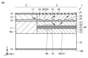
- FIG. 1 is a schematic cross-sectional view of a semiconductor optical gain element of Embodiment 1.
- FIG. 2 is a schematic partial enlarged sectional view of region IIA shown in FIG. 1 of the semiconductor optical gain device of Embodiment 1.
- FIG. 3 is a schematic partial enlarged cross-sectional view showing a first modification of the reflection section of the semiconductor optical gain element of Embodiment 1.
- FIG. 3 is a schematic partial enlarged cross-sectional view showing a second modification of the reflection section of the semiconductor optical gain element of the first embodiment.
- FIG. 3 is a schematic partially enlarged cross-sectional view showing one step of the method for manufacturing the passive part of the semiconductor optical gain device according to the first embodiment.
- FIG. 3 is a schematic partially enlarged cross-sectional view showing one step of the method for manufacturing the passive part of the semiconductor optical gain device according to the first embodiment.
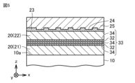
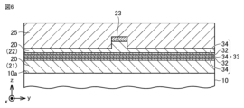
- FIG. 5 is a schematic partially enlarged cross-sectional view showing a step subsequent to the step shown in FIGS. 3 and 4 in the method for manufacturing the passive part of the semiconductor optical gain device according to the first embodiment.
- FIG. 5 is a schematic partially enlarged cross-sectional view showing a step subsequent to the step shown in FIGS. 3 and 4 in the method for manufacturing the passive part of the semiconductor optical gain device according to the first embodiment.
- FIG. 7 is a schematic partially enlarged cross-sectional view showing a step subsequent to the step shown in FIGS. 5 and 6 in the method for manufacturing the passive part of the semiconductor optical gain device of Embodiment 1.
- FIG. 5 is a schematic partially enlarged cross-sectional view showing a step subsequent to the step shown in FIGS. 3 and 4 in the method for manufacturing the passive part of the semiconductor optical gain device of Embodiment 1.
- FIG. 7 is a schematic partially enlarged cross-sectional view showing a step subsequent to the step shown in FIGS. 5 and 6 in the method for manufacturing the passive part of the semiconductor optical gain device of Embodiment 1.
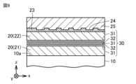
- FIG. FIG. 9 is a schematic partially enlarged cross-sectional view showing a step subsequent to the step shown in FIGS. 7 and 8 in the method for manufacturing the passive part of the semiconductor optical gain device according to the first embodiment.
- FIG. 9 is a schematic partially enlarged cross-sectional view showing a step subsequent to the step shown in FIGS. 7 and 8 in the method for manufacturing the passive part of the semiconductor optical gain device according to the first embodiment.
- FIG. 7 is a diagram showing a graph representing the reflectance of a reflective portion of a semiconductor optical gain element of a comparative example.
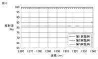
- FIG. 6 is a diagram showing a graph representing the reflectance of the reflecting portion of the semiconductor optical gain device of the first example, the second example, and the third example.
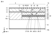
- FIG. 3 is a schematic cross-sectional view of a semiconductor optical gain device according to a second embodiment.
- 14 is a schematic partially enlarged cross-sectional view of region XIV shown in FIG. 13 of the semiconductor optical gain device of Embodiment 2.
- FIG. FIG. 7 is a schematic partially enlarged plan view of a reflection section of a semiconductor optical gain device according to a second embodiment.
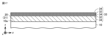
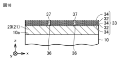
- FIG. 7 is a schematic partially enlarged cross-sectional view showing one step of a method for manufacturing a passive part of a semiconductor optical gain device according to a second embodiment.
- FIG. 7 is a schematic partially enlarged cross-sectional view showing one step of a method for manufacturing a passive part of a semiconductor optical gain device according to a second embodiment.
- FIG. 18 is a schematic partially enlarged cross-sectional view showing a step subsequent to the step shown in FIGS. 16 and 17 in a method for manufacturing a passive part of a semiconductor optical gain device according to a second embodiment.
- FIG. 18 is a schematic partially enlarged cross-sectional view showing a step subsequent to the step shown in FIGS. 16 and 17 in a method for manufacturing a passive part of a semiconductor optical gain device according to a second embodiment.
- FIG. 20 is a schematic partially enlarged sectional view showing a step subsequent to the step shown in FIGS.
- FIG. 20 is a schematic partially enlarged sectional view showing a step subsequent to the step shown in FIGS. 18 and 19 in a method for manufacturing a passive part of a semiconductor optical gain device according to a second embodiment.
- FIG. 22 is a schematic partially enlarged cross-sectional view showing a step subsequent to the step shown in FIGS. 20 and 21 in the method for manufacturing a passive part of a semiconductor optical gain device according to the second embodiment.
- FIG. 22 is a schematic partially enlarged cross-sectional view showing a step subsequent to the step shown in FIGS. 20 and 21 in the method for manufacturing a passive part of a semiconductor optical gain device according to the second embodiment.
- FIG. 22 is a schematic partially enlarged cross-sectional view showing a step subsequent to the step shown in FIGS. 20 and 21 in the method for manufacturing a passive part of a semiconductor optical gain device according to the second embodiment.
- FIG. 20 is a schematic partially enlarged sectional view showing a step subsequent to the step shown in FIGS. 20 and 21 in the method for manufacturing
- FIG. 24 is a schematic partially enlarged cross-sectional view showing a step subsequent to the step shown in FIGS. 22 and 23 in the method of manufacturing a passive part of a semiconductor optical gain device according to the second embodiment.
- FIG. 24 is a schematic partially enlarged cross-sectional view showing a step subsequent to the step shown in FIGS. 22 and 23 in the method of manufacturing a passive part of a semiconductor optical gain device according to the second embodiment.
- FIG. 3 is a schematic cross-sectional view of a semiconductor optical gain device according to a third embodiment.
- 27 is a schematic partial enlarged cross-sectional view taken along cross-sectional line XXVI-XXVI shown in FIG. 26 of the semiconductor optical gain device of Embodiment 3.
- FIG. 28 is a schematic partial enlarged cross-sectional view taken along cross-sectional line XXVIII-XXVIII shown in FIG. 27 of the semiconductor optical gain device of Embodiment 3.
- FIG. 28 is a schematic partial enlarged cross-sectional view taken along cross-sectional line XXIX-XXIX shown in FIG. 27 of the semiconductor optical gain device of Embodiment 3.
- FIG. 28 is a schematic partially enlarged cross-sectional view taken along the cross-sectional line XXX-XXX shown in FIG. 27 of the semiconductor optical gain device of Embodiment 3.
- FIG. FIG. 7 is a schematic partially enlarged cross-sectional view showing one step of a method for manufacturing a passive part of a semiconductor optical gain device according to a third embodiment.
- FIG. 7 is a schematic partially enlarged cross-sectional view showing one step of a method for manufacturing a passive part of a semiconductor optical gain device according to a third embodiment.
- FIG. 7 is a schematic partially enlarged cross-sectional view showing one step of a method for manufacturing a passive part of a semiconductor optical gain device according to a third embodiment.
- 34 is a schematic partially enlarged sectional view showing a step subsequent to the steps shown in FIGS. 31 to 33 in the method for manufacturing a passive part of a semiconductor optical gain device according to the third embodiment.
- FIG. 34 is a schematic partially enlarged sectional view showing a step subsequent to the steps shown in FIGS. 31 to 33 in the method for manufacturing a passive part of a semiconductor optical gain device according to the third embodiment.
- FIG. 34 is a schematic partially enlarged sectional view showing a step subsequent to the steps shown in FIGS. 31 to 33 in the method for manufacturing a passive part of a semiconductor optical gain device according to the third embodiment.
- FIG. 34 is a schematic partially enlarged sectional view showing a step subsequent to the steps shown in FIGS. 31 to 33 in the method for manufacturing a passive part of a semiconductor optical gain device according to the third embodiment.
- FIG. 37 is a schematic partially enlarged sectional view showing a step subsequent to the steps shown in FIGS. 34 to 36 in the method for manufacturing a passive part of a semiconductor optical gain device according to the third embodiment.
- FIG. 37 is a schematic partially enlarged sectional view showing a step subsequent to the steps shown in FIGS. 34 to 36 in the method for manufacturing a passive part of a semiconductor optical gain device according to the third embodiment.
- FIG. 37 is a schematic partially enlarged sectional view showing a step subsequent to the steps shown in FIGS.
- FIG. 40 is a schematic partially enlarged cross-sectional view showing a step subsequent to the steps shown in FIGS. 37 to 39 in the method for manufacturing a passive part of a semiconductor optical gain device according to the third embodiment.
- FIG. 40 is a schematic partially enlarged cross-sectional view showing a step subsequent to the steps shown in FIGS. 37 to 39 in the method for manufacturing a passive part of a semiconductor optical gain device according to the third embodiment.
- FIG. 40 is a schematic partially enlarged cross-sectional view showing a step subsequent to the steps shown in FIGS. 37 to 39 in the method for manufacturing a passive part of a semiconductor optical gain device according to the third embodiment.
- FIG. 40 is a schematic partially enlarged cross-sectional view showing a step subsequent to the steps shown in FIGS. 37 to 39 in the method for manufacturing a passive part of a semiconductor optical gain device according to the third embodiment.
- FIG. 40 is a schematic partially enlarged cross-sectional view showing a step subsequent to the steps shown in FIGS. 37 to 39 in the method
- FIG. 43 is a schematic partially enlarged cross-sectional view showing a step subsequent to the steps shown in FIGS. 40 to 42 in the method for manufacturing a passive part of a semiconductor optical gain device according to Embodiment 3.
- FIG. 43 is a schematic partially enlarged cross-sectional view showing a step subsequent to the steps shown in FIGS. 40 to 42 in the method for manufacturing a passive part of a semiconductor optical gain device according to Embodiment 3.
- FIG. 43 is a schematic partially enlarged cross-sectional view showing a step subsequent to the steps shown in FIGS. 40 to 42 in the method for manufacturing a passive part of a semiconductor optical gain device according to Embodiment 3.
- FIG. FIG. 7 is a schematic cross-sectional view of an optical semiconductor device according to a fourth embodiment.
- Embodiment 1 A semiconductor optical gain device 1 according to a first embodiment will be described with reference to FIGS. 1 and 2A.
- the semiconductor optical gain device 1 includes a substrate 10, an active part 2, and a passive part 3.
- a substrate 10 is a semiconductor substrate made of a compound semiconductor such as InP or GaAs, for example.
- Substrate 10 includes a main surface 10a and a main surface 10b opposite to main surface 10a.
- the main surface 10a and the main surface 10b each extend in the x direction and the y direction perpendicular to the x direction.
- the normal direction of the main surface 10a and the normal direction of the main surface 10b are the z direction perpendicular to the x direction and the y direction, respectively.
- active part 2 is formed on substrate 10.
- the active part 2 outputs light 17.
- the direction in which light 17 is emitted from the active region 2 is the x direction, and the width direction of the active region 2 is the y direction.
- Active section 2 includes a lower cladding layer 11, an active layer 12, an upper cladding layer 13, and electrodes 14 and 15.
- Lower cladding layer 11 is formed on main surface 10a of substrate 10 by, for example, epitaxial growth.
- the active layer 12 is formed on the lower cladding layer 11 by, for example, epitaxial growth.
- Upper cladding layer 13 is formed on active layer 12 by, for example, epitaxial growth.
- the electrode 14 is formed on the main surface 10b of the substrate 10 by, for example, vapor deposition.
- Electrode 15 is formed on upper cladding layer 13, for example by vapor deposition.
- the active layer 12 has a higher refractive index and a smaller band gap energy than the lower cladding layer 11 and the upper cladding layer 13.
- the active layer 12 is made of a compound semiconductor such as AlGaInAs or InGaAsP, for example.
- the lower cladding layer 11 and the upper cladding layer 13 are made of a compound semiconductor such as InP or GaAs, for example.
- Light 17 is output from the active layer 12 .
- the active part 2 is a laser diode or a semiconductor optical amplifier (SOA).
- the passive part 3 is formed on the main surface 10a of the substrate 10.
- the light propagation direction in the passive part 3 is the x direction, and the width direction of the passive part 3 is the y direction.
- the passive section 3 includes a lower cladding layer 20 , a first core layer 23 , an upper cladding layer 25 , an insulating layer 26 , and a reflective section 30 .
- the lower cladding layer 20 is formed on the main surface 10a of the substrate 10 by, for example, epitaxial growth.
- the lower cladding layer 20 is arranged between the first core layer 23 and the substrate 10.
- the lower cladding layer 20 includes a first lower cladding partial layer 21 and a second lower cladding partial layer 22 .
- the first lower cladding partial layer 21 is disposed between the reflective section 30 and the substrate 10 .
- the second lower cladding partial layer 22 is arranged between the reflective section 30 and the first core layer 23.
- the first core layer 23 is formed on the lower cladding layer 20 (more specifically, on the second lower cladding partial layer 22) by, for example, epitaxial growth.
- the longitudinal direction of the first core layer 23 is the x direction, and the width direction of the first core layer 23 is the y direction.
- First core layer 23 is optically coupled to active layer 12 .
- Light 17 output from the active layer 12 is coupled to the first core layer 23 and propagated through the first core layer 23 .
- Passive section 3 includes a passive waveguide.
- the upper cladding layer 25 is formed on the first core layer 23 by, for example, epitaxial growth.
- the insulating layer 26 is formed on the upper cladding layer 25 by, for example, chemical vapor deposition (CVD) or sputtering.
- the insulating layer 26 is a silicon oxide layer (SiO 2 layer).
- Insulating layer 26 includes top surface 27 of passive section 3 .
- the top surface 27 of the passive part 3 is a surface of the passive part 3 that is on the opposite side of the substrate 10 with respect to the first core layer 23 .
- the top surface 27 of the passive part 3 extends in the x direction and the y direction.
- the normal direction of the top surface 27 of the passive part 3 is the z direction.
- the first core layer 23 has a higher refractive index than the lower cladding layer 20 (more specifically, the second lower cladding partial layer 22) and the upper cladding layer 25.
- the first core layer 23 has a larger bandgap energy than the active layer 12.
- the first core layer 23 has a bandgap energy larger than the energy of the light 17 output from the active layer 12.
- the first core layer 23 is made of a compound semiconductor such as AlGaInAs or InGaAsP, for example.
- the lower cladding layer 20 and the upper cladding layer 25 are made of a compound semiconductor such as InP or GaAs, for example.
- the lower cladding layer 20 may be formed of the same material as the lower cladding layer 11.
- the upper cladding layer 25 may be formed of the same material as the upper cladding layer 13.
- a first grating coupler 24 is formed in the first core layer 23.
- the first grating coupler 24 diffracts the light 17 output from the active layer 12 and converts the first diffracted light 18 from the first grating coupler 24 toward the top surface 27 of the passive part 3 and the first diffracted light 18 from the first grating coupler 24 to the substrate. 10 (or the reflection section 30).
- the grating pitch of the first grating coupler 24 is set such that the second diffracted light 19 reflected by the reflection part 30 is emitted from the top surface 27 of the passive part 3 to the outside of the semiconductor optical gain element 1.
- the second diffracted light 19 reflected by the second diffracted light 19 is set so as not to be totally reflected by the top surface 27 of the passive part 3.
- the grating pitch of the first grating coupler 24 is shorter than the wavelength of the light 17, and the first grating coupler 24 is a short period grating.
- the incident angle of the second diffracted light 19 to the reflection section 30 is less than 18°
- the grating pitch of the first grating coupler 24 is less than 0.58 ⁇ m.
- the angle of incidence of the second diffracted light 19 on the reflecting section 30 is defined as the angle between the direction of incidence of the second diffracted light 19 on the reflecting section 30 and the normal line (z direction) of the reflecting section 30. be done.
- the reflecting section 30 is arranged between the first grating coupler 24 and the substrate 10.
- the reflective section 30 is arranged in the lower cladding layer 20. Specifically, the reflective section 30 is formed on the first lower cladding partial layer 21 and is arranged between the first lower cladding partial layer 21 and the second lower cladding partial layer 22 .
- the reflecting section 30 reflects the second diffracted light 19 generated by the first grating coupler 24 toward the top surface 27 of the passive section 3 . Therefore, among the light 17 output from the active layer 12, the light (first diffracted light 18 and second diffracted light 19) that is diffracted by the first grating coupler 24 is transmitted from the top surface 27 of the passive section 3 to the semiconductor optical gain element. It is emitted to the outside of 1.
- the reflective section 30 is, for example, a multilayer reflective film in which air layers 31 as low refractive index layers and semiconductor layers 32 as high refractive index layers are alternately laminated.
- the reflecting section 30 is, for example, a distributed Bragg reflector (DBR).
- DBR distributed Bragg reflector
- the number of air layers 31 included in the reflecting section 30 is not limited to two or more, and may be one as shown in FIGS. 2B and 2C. That is, the reflecting section 30 only needs to include at least one air layer 31.
- one air layer 31 may be placed between two semiconductor layers 32 as shown in FIG. 2B, or one air layer 31 may be placed between two semiconductor layers 32 as shown in FIG. 2C.
- FIG. 1 and 2A the reflective section 30 is, for example, a multilayer reflective film in which air layers 31 as low refractive index layers and semiconductor layers 32 as high refractive index layers are alternately laminated.
- the reflecting section 30 is, for example, a distributed Bragg reflector (DBR).
- the semiconductor layer 32 may not be included in the reflective portion 30 and one air layer 31 may be disposed between the first lower cladding portion layer 21 and the second lower cladding portion layer 22.
- the number of air layers 31 included in the reflective section 30 is two, the number of semiconductor layers 32 included in the reflective section 30 is one or more.
- the reflective section 30 includes a plurality of semiconductor layers 32.
- the semiconductor layer 32 may be formed of the same material as the lower cladding layer 20.
- the semiconductor layer 32 may be formed of the same material as the first lower cladding partial layer 21 or the same material as the second lower cladding partial layer 22.
- the semiconductor layer 32 is made of a compound semiconductor such as InP or GaAs, for example.
- the semiconductor layer 32 is supported by, for example, the lower cladding layer 11.
- the thickness of the air layer 31 and the thickness of the semiconductor layer 32 are set, for example, so that the reflectance of the reflection section 30 for the second diffracted light 19 is maximized.
- the thickness of the semiconductor layer 32 may be larger than the reference thickness, which is the thickness of the semiconductor layer 32 at which the reflectance of the reflection section 30 for the second diffracted light 19 becomes maximum. Therefore, the mechanical strength of the reflecting section 30 is improved, and the mechanical strength of the semiconductor optical gain element 1 is improved.
- the active portion 2 of the semiconductor optical gain device 1 is manufactured by a known method.
- An example of a method for manufacturing the passive section 3 of the semiconductor optical gain device 1 of this embodiment will be described with reference to FIGS. 3 to 10.
- a first lower cladding partial layer 21 is formed on the main surface 10a of the substrate 10 by epitaxial growth.
- the first lower cladding portion layer 21 is made of a compound semiconductor such as InP or GaAs, for example.
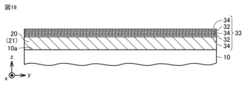
- a multilayer film 33 is formed on the main surface 10a of the substrate 10 by epitaxial growth.
- the multilayer film 33 is formed by alternately stacking semiconductor layers 32 and sacrificial layers 34.
- the sacrificial layer 34 is formed of a material having a higher etching rate than the semiconductor layer 32 with respect to the etchant used in the etching process shown in FIGS. 9 and 10.
- the semiconductor layer 32 is formed of a compound semiconductor such as InP or GaAs.
- the sacrificial layer 34 is made of a compound semiconductor such as InGaAsP, AlGaInAs, InGaAs, or AlInAs.
- the second lower cladding partial layer 22 is formed on the multilayer film 33 by epitaxial growth.
- the second lower cladding partial layer 22 is made of the same material as the first lower cladding partial layer 21, for example.
- the second lower cladding partial layer 22 is made of a compound semiconductor such as InP or GaAs, for example.
- a first core layer 23 is formed on the lower cladding layer 20 by epitaxial growth. By etching the second lower cladding partial layer 22 and the first core layer 23, a mesa structure is formed in the second lower cladding partial layer 22 and the first core layer 23.
- a first grating coupler 24 is formed in the first core layer 23 by etching the first core layer 23 .
- An upper cladding layer 25 is formed on the second lower cladding partial layer 22 and the first core layer 23 by epitaxial growth. The mesa structure is filled with an upper cladding layer 25.
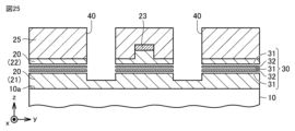
- grooves 40 are formed on both sides of the first core layer 23 by etching the upper cladding layer 25, the second lower cladding partial layer 22, the multilayer film 33, and the first lower cladding partial layer 21. form.
- the groove 40 a portion of the multilayer film 33 is exposed.
- a hole may be formed instead of the groove 40.
- an etchant for example, an etching solution
- the sacrificial layer 34 of the multilayer film 33 is selectively etched by the etchant. Since the semiconductor layer 32 has a lower etching rate with respect to the etchant than the sacrificial layer 34, it is hardly etched by the etchant.
- the sacrificial layer 34 becomes the air layer 31, and the multilayer film 33 becomes the reflective section 30.
- An insulating layer 26 is formed on the upper cladding layer 25 by chemical vapor deposition (CVD), sputtering, or the like. In this way, the passive section 3 of the semiconductor optical gain device 1 is obtained.
- the operation of the semiconductor optical gain device 1 will be explained.
- a current is injected into the active layer 12 from the electrodes 14 and 15, a stimulated emission phenomenon occurs in the active layer 12.
- Light 17 is output from the active layer 12 .
- Light 17 couples to first core layer 23 and propagates through first core layer 23 .
- the first grating coupler 24 diffracts the light 17 to generate a first diffracted light 18 and a second diffracted light 19.
- the reflecting section 30 reflects the second diffracted light 19 toward the top surface 27 of the passive section 3 .
- the first diffracted light 18 and the second diffracted light 19 are emitted from the top surface 27 of the passive section 3 .
- the operation of the semiconductor optical gain device 1 will be explained.
- the first diffracted light 18 passes through the upper cladding layer 25 and is emitted from the semiconductor optical gain element 1 .
- the second diffracted light 19 passes through the second lower cladding partial layer 22 , the first core layer 23 , and the upper cladding layer 25 and is emitted from the semiconductor optical gain device 1 .
- the thickness of the upper cladding layer 25, the thickness of the first core layer 23, and the thickness of the second lower cladding partial layer 22 are each sufficiently smaller than the thickness of the substrate 10. Therefore, the thickness variations of the upper cladding layer 25, the thickness variations of the first core layer 23, and the thickness variations of the second lower cladding partial layer 22 are each larger than the thickness variations of the substrate 10. Small enough.
- the first diffracted light 18 and the second diffracted light 19 are emitted from the semiconductor optical gain element 1 without passing through the substrate 10, which has the largest variation in thickness among the semiconductor optical gain elements 1. Variations in the emission positions of the first diffracted light 18 and the second diffracted light 19 from the semiconductor optical gain element 1 are reduced.
- the mounting precision of semiconductor optical gain element 1 to optical waveguide chip 6 can be relaxed.
- the reflecting section 30 includes at least one air layer 31, the reflectance of the reflecting section 30 with respect to the second diffracted light 19 increases. Therefore, the efficiency of optical coupling from the semiconductor optical gain element 1 to the optical waveguide chip 6 can be improved.
- the semiconductor optical gain device of the comparative example has the same configuration as the semiconductor optical gain device 1 of the present embodiment, but the configuration of the reflecting section 30 is different.
- the reflective section 30 is a multilayer reflective film in which InGaAsP layers as high refractive index layers and InP layers as low refractive index layers are alternately laminated.
- the reflective section 30 of the comparative example does not include the air layer 31 as a low refractive index layer.
- the reflective section 30 of the comparative example has a thirty-layer structure.
- the wavelength of the second diffracted light 19 is 1300 nm
- the refractive index of the InGaAsP layer is 3.41
- the refractive index of the InP layer is 3.21
- the angle of incidence of the second diffracted light 19 on the reflection section 30 is 12.7. °.
- the thickness of the InGaAsP layer and the thickness of the InP layer are set so that the reflectance of the reflection section 30 for the second diffracted light 19 is maximized. As shown in FIG. 11, the reflectance of the reflective section 30 of the comparative example with respect to the second diffracted light 19 is about 55%.
- the reflection section 30 includes an InP layer as a high refractive index layer (semiconductor layer 32), an air layer 31 as a low refractive index layer, and a high refractive index layer (Semiconductor layer 32), an air layer 31 as a low refractive index layer, and a high refractive index layer (Semiconductor layer 32), which an InP layer (as a semiconductor layer 32) is laminated. That is, the air layer 31 included in the reflective section 30 of the first embodiment is one layer, the InP layer (semiconductor layer 32) included in the reflective section 30 of the first embodiment is two layers, and the air layer 31 included in the reflective section 30 of the first embodiment is two layers.
- the reflective section 30 has a three-layer structure.
- the reflection section 30 includes an InP layer as a high refractive index layer (semiconductor layer 32) and an air layer as a low refractive index layer.
- This is a multilayer reflective film in which 31 and 31 are alternately laminated.
- the air layer 31 included in the reflective section 30 of the second embodiment is two layers
- the InP layer (semiconductor layer 32) included in the reflective section 30 of the second embodiment is three layers
- the reflective section 30 of the second embodiment has three layers.
- the section 30 has a five-layer structure.
- the air layer 31 included in the reflective section 30 of the third embodiment is three layers
- the InP layer (semiconductor layer 32) included in the reflective section 30 of the third embodiment is four layers
- the reflective section 30 of the third embodiment has four layers.
- the section 30 has a seven-layer structure.
- the wavelength of the second diffracted light 19 is 1300 nm
- the refractive index of the air layer 31 is 1.00
- the refractive index of the InP layer is 3.21
- the reflective part 30 is The angle of incidence of the second diffracted light 19 on the second diffracted light 19 is assumed to be 12.7°.
- the thickness of the air layer 31 and the thickness of the InP layer are set so that the reflectance of the reflection section 30 for the second diffracted light 19 is maximized. As shown in FIG.
- the reflectance of the reflecting section 30 of the first embodiment with respect to the second diffracted light 19 is about 81.5%, and the reflectance of the reflecting section 30 of the second embodiment with respect to the second diffracted light 19 is approximately 81.5%.
- the reflectance is about 98.9%, and the reflectance of the reflecting section 30 of the third embodiment for the second diffracted light 19 is about 99.9%.
- the reflectance of the reflection part 30 for the second diffracted light 19 is greatly improved by including the at least one air layer 31 in the reflection part 30.
- the reason for this is that in each of the first to third embodiments, the low refractive index layer (air layer 31) of the reflective section 30 and the layer adjacent to the low refractive index layer (for example, the high refractive index layer of the reflective section 30) (InP layer of the reflective section 30 which is the semiconductor layer 32), the refractive index difference between the low refractive index layer (for example, InP layer) of the reflective section 30 in the comparative example and the layer adjacent to the low refractive index layer ( This is because the refractive index difference is larger than the refractive index difference between the high refractive index layer (InGaAsP layer of the reflective section 30) and the high refractive index layer of the reflective section 30. Therefore, the optical coupling efficiency from the semiconductor optical gain element 1 to the optical waveguide chip 6 (see FIG. 46)
- the reflectance of the reflecting section 30 for the second diffracted light 19 is further improved. . Therefore, the optical coupling efficiency from the semiconductor optical gain element 1 to the optical waveguide chip 6 (see FIG. 46) is further improved.
- the semiconductor optical gain device 1 of this embodiment includes a substrate 10, an active section 2 formed on the substrate 10, and a passive section 3 formed on the substrate 10.
- Active section 2 includes an active layer 12 .
- the passive part 3 includes a first core layer 23 optically coupled to the active layer 12 , a reflective part 30 , and a top surface 27 on the opposite side of the substrate 10 with respect to the first core layer 23 .
- a first grating coupler 24 is formed in the first core layer 23 .
- the first grating coupler 24 diffracts the light 17 output from the active layer 12 to produce a first diffracted light 18 directed from the first grating coupler 24 toward the top surface 27 and a first diffracted light 18 directed from the first grating coupler 24 toward the substrate 10. 2 diffracted light 19 is generated.
- the reflecting section 30 is arranged between the first grating coupler 24 and the substrate 10, and reflects the second diffracted light 19 toward the top surface 27 of the passive section 3, and also reflects at least one air layer 31. include.
- the semiconductor optical gain element 1 includes the reflecting section 30, not only the first diffracted light 18 but also the second diffracted light 19 are emitted from the top surface 27 of the passive section 3.
- the first diffracted light 18 and the second diffracted light 19 are emitted from the semiconductor optical gain element 1 without passing through the substrate 10, which has the largest variation in thickness among the semiconductor optical gain elements 1. Therefore, variations in the emission positions of the first diffracted light 18 and the second diffracted light 19 from the semiconductor optical gain element 1 are reduced.
- the mounting precision of the semiconductor optical gain device 1 on the optical waveguide chip 6 can be relaxed.
- the reflecting section 30 includes at least one air layer 31, the reflectance of the reflecting section 30 with respect to the second diffracted light 19 increases. Therefore, the efficiency of optical coupling from the semiconductor optical gain element 1 to the optical waveguide chip 6 can be improved.
- At least one air layer 31 is a plurality of air layers 31.
- the reflective section 30 is a multilayer reflective film including a plurality of air layers 31 and at least one semiconductor layer 32.
- the reflecting section 30 includes the plurality of air layers 31, the reflectance of the reflecting section 30 for the second diffracted light 19 further increases. Therefore, the optical coupling efficiency from the semiconductor optical gain element 1 to the optical waveguide chip 6 can be further improved.
- the reflecting section 30 is a distributed Bragg reflector. Therefore, the mounting precision of the semiconductor optical gain device 1 to the optical waveguide chip 6 can be relaxed, and the optical coupling efficiency from the semiconductor optical gain device 1 to the optical waveguide chip 6 can be improved.
- the first grating coupler 24 has a grating pitch of less than 0.58 ⁇ m.
- the second diffracted light 19 is emitted to the outside of the semiconductor optical gain element 1 without being totally reflected on the top surface 27 of the passive section 3.
- the optical coupling efficiency from the semiconductor optical gain element 1 to the optical waveguide chip 6 can be improved.
- Embodiment 2 A semiconductor optical gain device 1b according to a second embodiment will be described with reference to FIGS. 13 and 14.
- the semiconductor optical gain device 1b of this embodiment has the same configuration as the semiconductor optical gain device 1 of the first embodiment, but differs mainly in the following points.
- the passive section 3 further includes a support member 36.
- the support member 36 extends through the air layer 31 from the first lower cladding partial layer 21 to the second lower cladding partial layer 22 .
- the support member 36 supports the second lower cladding portion layer 22 and the semiconductor layer 32.
- the support member 36 is disposed within the reflective portion 30 in a plan view of the top surface 27 of the passive portion 3 .
- a hole 37 is formed in the reflective section 30.
- a support member 36 is formed within the bore 37.
- a groove may be formed in the multilayer film 33, and the support member 36 may be formed within the groove.
- the support member 36 is, for example, a support column or a support wall.
- the support member 36 is made of, for example, a semiconductor. Support member 36 may be formed of the same material as semiconductor layer 32. Support member 36 may be formed of the same material as lower cladding layer 20. The support member 36 may be formed of the same material as the first lower cladding partial layer 21 or the same material as the second lower cladding partial layer 22, for example. The support member 36 is made of a compound semiconductor such as InP or GaAs, for example.
- the number of air layers 31 included in the reflecting section 30 is not limited to two or more, and may be one. That is, the reflecting section 30 only needs to include at least one air layer 31.
- the semiconductor layer 32 may not be included in the reflective section 30, and the supporting member 36 may support the second lower cladding partial layer 22. good.
- the method for manufacturing the passive section 3 of the semiconductor optical gain device 1b of the present embodiment includes the same steps as the method of manufacturing the passive section 3 of the semiconductor optical gain device 1 of the first embodiment, but is different from the embodiment in the following points.
- the method for manufacturing the passive section 3 of the semiconductor optical gain device 1 of the first embodiment is different from that of the first embodiment.
- the main surface 10a of the substrate 10 is manufactured by a process similar to that shown in FIGS.
- a first lower cladding partial layer 21 and a multilayer film 33 are formed thereon.
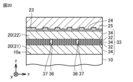
- the multilayer film 33 is etched to form holes 37 in the multilayer film 33.
- a support member 36 is formed in the hole 37 by, for example, epitaxial growth.
- a groove may be formed in the multilayer film 33 instead of the hole 37, and the support member 36 may be formed within the groove.
- Support member 36 is formed within multilayer membrane 33 .
- the support member 36 is formed of a material having a lower etching rate than the sacrificial layer 34 with respect to the etchant used in the etching process shown in FIGS. 24 and 25.
- the support member 36 is made of a compound semiconductor such as InP or GaAs, for example.
- multilayer film 33 and support member 36 a second lower cladding partial layer 22, a first core layer 23, and an upper cladding layer 25 are formed.
- a first grating coupler 24 is formed in the first core layer 23 .
- first core layer 23 is formed by the same steps as those shown in FIGS. 7 and 8 in the method for manufacturing passive part 3 of semiconductor optical gain device 1 of the first embodiment.
- Grooves 40 are formed on both sides. Instead of the groove 40, a hole may be formed. In the groove 40, a portion of the multilayer film 33 is exposed.
- groove 40 is filled with an etchant (e.g. , etching solution) to selectively etch the sacrificial layer 34 of the multilayer film 33 with the etchant. Since the semiconductor layer 32 and the support member 36 have a lower etching rate with respect to the etchant than the sacrificial layer 34, they are hardly etched by the etchant.
- the sacrificial layer 34 becomes the air layer 31, and the multilayer film 33 becomes the reflective section 30.
- An insulating layer 26 is formed on the upper cladding layer 25 by chemical vapor deposition (CVD), sputtering, or the like. In this way, the passive part 3 of the semiconductor optical gain element 1b is obtained.
- CVD chemical vapor deposition
- the semiconductor optical gain element 1b of this embodiment has the following effects.
- the passive section 3 includes a lower cladding layer 20 disposed between the first core layer 23 and the substrate 10, and a support member 36.
- the lower cladding layer 20 includes a first lower cladding partial layer 21 disposed between the reflective section 30 and the substrate 10 and a second lower cladding layer disposed between the reflective section 30 and the first core layer 23.
- the partial layer 22 is included.
- the support member 36 extends from the first lower cladding partial layer 21 to the second lower cladding partial layer 22, supports the second lower cladding partial layer 22, and is reflective in a plan view of the top surface 27 of the passive part 3. It is arranged in the section 30.
- the mechanical strength of the reflecting section 30 is improved by the support member 36. Therefore, damage to the semiconductor optical gain element 1b can be prevented during manufacture of the semiconductor optical gain element 1b. The manufacturing yield of the semiconductor optical gain device 1b is improved. Furthermore, damage to the semiconductor optical gain element 1b due to thermal stress applied to the semiconductor optical gain element 1b can be prevented while the semiconductor optical gain element 1b is used for a long period of time. The life of the semiconductor optical gain element 1b is extended.
- the passive section 3 includes a lower cladding layer 20 disposed between the first core layer 23 and the substrate 10, and a support member 36.
- the lower cladding layer 20 includes a first lower cladding partial layer 21 disposed between the reflective section 30 and the substrate 10 and a second lower cladding layer disposed between the reflective section 30 and the first core layer 23.
- the partial layer 22 is included.
- the support member 36 extends from the first lower cladding part layer 21 to the second lower cladding part layer 22, supports the second lower cladding part layer 22 and at least one semiconductor layer 32, and supports the passive part 3. It is arranged in the reflecting section 30 when viewed from above on the top surface 27 .
- the mechanical strength of the reflecting section 30 is improved by the support member 36. Therefore, damage to the semiconductor optical gain element 1b can be prevented during manufacture of the semiconductor optical gain element 1b. The manufacturing yield of the semiconductor optical gain device 1b is improved. Furthermore, damage to the semiconductor optical gain element 1b due to thermal stress applied to the semiconductor optical gain element 1b can be prevented while the semiconductor optical gain element 1b is used for a long period of time. The life of the semiconductor optical gain element 1b is extended.
- Embodiment 3 A semiconductor optical gain device 1c according to the third embodiment will be described with reference to FIGS. 26 to 30.
- the semiconductor optical gain device 1c of this embodiment has the same configuration as the semiconductor optical gain device 1 of the first embodiment, but differs mainly in the following points.
- the reflective portion 30 is smaller than the top surface 27 of the passive portion 3 when viewed from above.
- the reflective part 30 is smaller than the upper cladding layer 25.
- the reflecting section 30 is selectively formed in a region where the second diffracted light 19 is distributed in a plan view of the top surface 27 of the passive section 3.
- the passive part 3 further includes a support member 36.
- the support member 36 extends from the first lower cladding partial layer 21 to the second lower cladding partial layer 22 .
- the support member 36 supports the second lower cladding portion layer 22 and the semiconductor layer 32.
- the support member 36 is arranged around the reflective section 30 when viewed from above on the top surface 27 of the passive section 3 .
- a hole 38 communicating with the air layer 31 of the reflection section 30 is provided in the support member 36 .
- the support member 36 is, for example, a wall, and the hole 38 is provided in the wall.
- the air layer 31 and semiconductor layer 32 that constitute the reflective section 30 are also present within the hole 38 .
- the support member 36 may be made of a semiconductor, for example.
- the support member 36 may be formed of the same material as the semiconductor layer 32, for example.
- the support member 36 may be formed of the same material as the lower cladding layer 20, for example.
- the support member 36 may be formed of the same material as the first lower cladding partial layer 21 or the same material as the second lower cladding partial layer 22, for example.
- the support member 36 is made of a compound semiconductor such as InP or GaAs, for example.
- the number of air layers 31 included in the reflecting section 30 is not limited to two or more, and may be one. That is, the reflecting section 30 only needs to include at least one air layer 31.
- the semiconductor layer 32 may not be included in the reflective section 30, and the supporting member 36 may support the second lower cladding partial layer 22. good.
- FIGS. 31 to 45 An example of a method for manufacturing the passive section 3 of the semiconductor optical gain device 1c of this embodiment will be described with reference to FIGS. 31 to 45.
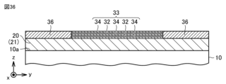
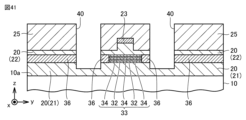
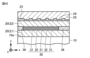
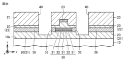
- 32, FIG. 35, FIG. 38, FIG. 41, and FIG. 44 are schematic partial enlarged sectional views of a portion of the passive part 3 corresponding to FIG. 29. 33, FIG. 36, FIG. 39, FIG. 42, and FIG. 45 are schematic partial enlarged sectional views of a portion of the passive part 3 corresponding to FIG. 30.
- the method for manufacturing the passive portion 3 of the semiconductor optical gain device 1c of the present embodiment includes the same steps as the method of manufacturing the passive portion 3 of the semiconductor optical gain device 1 of the first embodiment, but is different from the method in the following points.
- the method for manufacturing the passive section 3 of the semiconductor optical gain device 1 of the first embodiment is different from that of the first embodiment.
- the main surface 10a of the substrate 10 is manufactured by a process similar to that shown in FIGS.
- a first lower cladding partial layer 21 and a multilayer film 33 are formed thereon.
- the multilayer film 33 is etched.
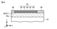
- a support member 36 is formed around the multilayer film 33 by, for example, epitaxial growth.
- Support member 36 is formed around multilayer film 33 .
- a hole 38 (see FIG. 27) is provided in the support member 36, and the multilayer film 33 is also located within the hole 38.
- the support member 36 is formed of a material that has a lower etching rate than the sacrificial layer 34 with respect to the etchant used in the etching process shown in FIGS. 43 to 45.
- the support member 36 is made of a compound semiconductor such as InP or GaAs, for example.
- the multilayer film 33 and the support member are manufactured by the same steps as those shown in FIGS. 36, a second lower cladding partial layer 22, a first core layer 23, and an upper cladding layer 25 are formed.
- a first grating coupler 24 is formed in the first core layer 23 .
- the upper cladding layer 25, the second lower Grooves 40 are formed on both sides of the first core layer 23 by etching the cladding partial layer 22, the multilayer film 33, the support member 36, and the first lower cladding partial layer 21.
- Grooves 40 formed on both sides of the first core layer 23 are connected to holes 38 in the support member 36 .
- a portion of the multilayer film 33 is exposed. Instead of the groove 40, a hole may be formed.
- grooves 40 are filled with an etchant (for example, , etching solution) to selectively etch the sacrificial layer 34 of the multilayer film 33 with the etchant.
- the etchant flows into the inside of the support member 36 through the holes 38 in the support member 36 while etching the sacrificial layer 34 . Since the semiconductor layer 32 and the support member 36 have a lower etching rate with respect to the etchant than the sacrificial layer 34, they are hardly etched by the etchant.
- the sacrificial layer 34 becomes the air layer 31, and the multilayer film 33 becomes the reflective section 30. Air layer 31 communicates with hole 38 and groove 40 .
- An insulating layer 26 is formed on the upper cladding layer 25 by chemical vapor deposition (CVD), sputtering, or the like. In this way, the passive part 3 of the semiconductor optical gain element 1c is obtained.
- the semiconductor optical gain element 1c of this embodiment has the following effects.
- the passive section 3 includes a lower cladding layer 20 disposed between the first core layer 23 and the substrate 10, and a support member 36.
- the lower cladding layer 20 includes a first lower cladding partial layer 21 disposed between the reflective section 30 and the substrate 10 and a second lower cladding layer disposed between the reflective section 30 and the first core layer 23.
- the partial layer 22 is included.
- the support member 36 extends from the first lower cladding partial layer 21 to the second lower cladding partial layer 22, supports the second lower cladding partial layer 22, and is reflective in a plan view of the top surface 27 of the passive part 3. are arranged around the section 30.
- the mechanical strength of the reflecting section 30 is improved by the support member 36. Therefore, damage to the semiconductor optical gain element 1c can be prevented during manufacture of the semiconductor optical gain element 1c. The manufacturing yield of the semiconductor optical gain device 1c is improved. Furthermore, damage to the semiconductor optical gain element 1c due to thermal stress applied to the semiconductor optical gain element 1c can be prevented while the semiconductor optical gain element 1c is used for a long period of time. The life of the semiconductor optical gain element 1c is extended.
- the passive section 3 includes a lower cladding layer 20 disposed between the first core layer 23 and the substrate 10, and a support member 36.
- the lower cladding layer 20 includes a first lower cladding partial layer 21 disposed between the reflective section 30 and the substrate 10 and a second lower cladding layer disposed between the reflective section 30 and the first core layer 23.
- the partial layer 22 is included.
- the support member 36 extends from the first lower cladding part layer 21 to the second lower cladding part layer 22, supports the second lower cladding part layer 22 and at least one semiconductor layer 32, and supports the passive part 3. They are arranged around the reflective section 30 in a plan view of the top surface 27 .
- the mechanical strength of the reflecting section 30 is improved by the support member 36. Therefore, damage to the semiconductor optical gain element 1c can be prevented during manufacture of the semiconductor optical gain element 1c. The manufacturing yield of the semiconductor optical gain device 1c is improved. Furthermore, damage to the semiconductor optical gain element 1c due to thermal stress applied to the semiconductor optical gain element 1c can be prevented while the semiconductor optical gain element 1c is used for a long period of time. The life of the semiconductor optical gain element 1c is extended.
- the support member 36 is provided with a hole 38 that communicates with at least one air layer 31.
- the etchant is applied to the support member 36 from the hole 38 of the support member 36 while etching the sacrificial layer 34. flows inside.
- the manufacturing of the reflective section 30 including the air layer 31 is facilitated.
- Optical semiconductor device 5 includes semiconductor optical gain element 1 of Embodiment 1, optical waveguide chip 6, and bonding member 50.
- the optical waveguide chip 6 includes a substrate 43, a lower cladding layer 44, a second core layer 45, an upper cladding layer 47, and a top surface 48.
- the substrate 43 is, for example, a semiconductor substrate such as a Si substrate.
- Substrate 43 may be formed of a different material from substrate 10.
- the lower cladding layer 44 is formed on the substrate 43 by, for example, chemical vapor deposition (CVD) or sputtering.
- the lower cladding layer 44 is arranged between the second core layer 45 and the substrate 43.
- the lower cladding layer 44 is, for example, a silicon oxide layer (SiO 2 layer).
- the second core layer 45 is formed on the lower cladding layer 44 by, for example, chemical vapor deposition (CVD) or sputtering.
- the second core layer 45 has a higher refractive index than the lower cladding layer 44 and the upper cladding layer 47.
- the second core layer 45 is made of a different material from the first core layer 23, for example.
- the second core layer 45 is made of silicon (Si) or silicon nitride (Si 3 N 4 ), for example.
- the refractive index difference between the second core layer 45 and the upper cladding layer 47 and the refractive index difference between the second core layer 45 and the lower cladding layer 44 are different from that between the first core layer 23 and the upper cladding layer 47, respectively.
- the light confinement in the second core layer 45 in the optical waveguide chip 6 may be stronger than the light confinement in the first core layer 23 in the passive part 3 chip.
- the upper cladding layer 47 is formed on the second core layer 45 by, for example, chemical vapor deposition (CVD) or sputtering.
- the upper cladding layer 47 is, for example, a silicon oxide layer (SiO 2 layer).
- the top surface 48 of the optical waveguide chip 6 is the surface of the optical waveguide chip 6 that is opposite to the substrate 43 .
- Upper cladding layer 47 includes a top surface 48 .
- a second grating coupler 46 that optically couples to the first grating coupler 24 is formed in the second core layer 45 .
- the second grating coupler 46 is formed, for example, by etching the second core layer 45.
- the first diffracted light 18 and the second diffracted light 19 are coupled to the second grating coupler 46 and propagate through the second core layer 45 .
- the semiconductor optical gain element 1c is flip-chip mounted to the optical waveguide chip 6 using a bonding member 50.
- the top surface 27 of the passive part 3 is arranged facing the optical waveguide chip 6 (more specifically, the top surface 48).
- the joining member 50 is, for example, an Au bump or solder.
- the operation of the optical semiconductor device 5 will be explained.
- a current is injected into the active layer 12 from the electrodes 14 and 15, a stimulated emission phenomenon occurs in the active layer 12.
- Light 17 is output from the active layer 12 .
- Light 17 couples to first core layer 23 and propagates through first core layer 23 .
- the first grating coupler 24 diffracts the light 17 to generate a first diffracted light 18 and a second diffracted light 19.
- the reflecting section 30 reflects the second diffracted light 19 toward the top surface 27 of the passive section 3 .
- the first diffracted light 18 and the second diffracted light 19 are emitted from the top surface 27 of the passive section 3 .
- the first diffracted light 18 and the second diffracted light 19 are coupled to the second grating coupler 46 and propagate through the second core layer 45 .
- the optical semiconductor device 5 includes the semiconductor optical gain element 1b of the second embodiment or the semiconductor optical gain element 1c of the third embodiment instead of the semiconductor optical gain element 1 of the first embodiment. may be provided.
- the optical semiconductor device 5 of this embodiment includes semiconductor optical gain elements 1, 1b, and 1c, and an optical waveguide chip 6 disposed facing the top surface 27 of the passive section 3.
- Optical waveguide chip 6 includes a second core layer 45 .
- a second grating coupler 46 that optically couples to the first grating coupler 24 is formed in the second core layer 45 .
- the mounting precision of the semiconductor optical gain elements 1, 1b, 1c to the optical waveguide chip 6 can be relaxed, and the optical coupling efficiency from the semiconductor optical gain elements 1, 1b, 1c to the optical waveguide chip 6 can be improved.
- the first core layer 23 is formed of a compound semiconductor.
- the second core layer 45 is made of silicon (Si) or silicon nitride (Si 3 N 4 ).
- the second core layer 45 is formed of a different material from the first core layer 23
- the mounting accuracy of the semiconductor optical gain elements 1, 1b, 1c on the optical waveguide chip 6 can be relaxed, and the semiconductor optical The optical coupling efficiency from the gain elements 1, 1b, 1c to the optical waveguide chip 6 can be improved.
- Embodiments 1-4 disclosed this time should be considered to be illustrative in all respects and not restrictive. Unless there is a contradiction, at least two of the embodiments 1 to 4 disclosed herein may be combined.
- the scope of the present disclosure is indicated by the claims rather than the above description, and is intended to include meanings equivalent to the claims and all changes within the range.
Landscapes
- Physics & Mathematics (AREA)
- General Physics & Mathematics (AREA)
- Optics & Photonics (AREA)
- Condensed Matter Physics & Semiconductors (AREA)
- Electromagnetism (AREA)
- Geometry (AREA)
- Engineering & Computer Science (AREA)
- Microelectronics & Electronic Packaging (AREA)
- Optical Integrated Circuits (AREA)
- Semiconductor Lasers (AREA)
- Optical Couplings Of Light Guides (AREA)
Priority Applications (4)
| Application Number | Priority Date | Filing Date | Title |
|---|---|---|---|
| CN202280097574.8A CN119452282A (zh) | 2022-07-08 | 2022-07-08 | 半导体光增益元件以及光半导体装置 |
| JP2022560307A JP7199617B1 (ja) | 2022-07-08 | 2022-07-08 | 半導体光利得素子及び光半導体装置 |
| PCT/JP2022/027114 WO2024009502A1 (ja) | 2022-07-08 | 2022-07-08 | 半導体光利得素子及び光半導体装置 |
| US18/876,678 US20250372954A1 (en) | 2022-07-08 | 2022-07-08 | Semiconductor optical gain device and optical semiconductor apparatus |
Applications Claiming Priority (1)
| Application Number | Priority Date | Filing Date | Title |
|---|---|---|---|
| PCT/JP2022/027114 WO2024009502A1 (ja) | 2022-07-08 | 2022-07-08 | 半導体光利得素子及び光半導体装置 |
Publications (1)
| Publication Number | Publication Date |
|---|---|
| WO2024009502A1 true WO2024009502A1 (ja) | 2024-01-11 |
Family
ID=84784189
Family Applications (1)
| Application Number | Title | Priority Date | Filing Date |
|---|---|---|---|
| PCT/JP2022/027114 Ceased WO2024009502A1 (ja) | 2022-07-08 | 2022-07-08 | 半導体光利得素子及び光半導体装置 |
Country Status (4)
| Country | Link |
|---|---|
| US (1) | US20250372954A1 (https=) |
| JP (1) | JP7199617B1 (https=) |
| CN (1) | CN119452282A (https=) |
| WO (1) | WO2024009502A1 (https=) |
Citations (4)
| Publication number | Priority date | Publication date | Assignee | Title |
|---|---|---|---|---|
| JP2001358403A (ja) * | 2000-06-12 | 2001-12-26 | Nippon Telegr & Teleph Corp <Ntt> | 面発光レーザ |
| US20140003458A1 (en) * | 2012-06-28 | 2014-01-02 | Yale University | Lateral electrochemical etching of iii-nitride materials for microfabrication |
| US20150260913A1 (en) * | 2012-08-17 | 2015-09-17 | Oracle International Corporation | Grating coupler for inter-chip optical coupling |
| JP2019500753A (ja) * | 2015-12-17 | 2019-01-10 | フィニサー コーポレイション | 表面結合システム |
Family Cites Families (2)
| Publication number | Priority date | Publication date | Assignee | Title |
|---|---|---|---|---|
| US20180081118A1 (en) * | 2014-07-14 | 2018-03-22 | Biond Photonics Inc. | Photonic integration by flip-chip bonding and spot-size conversion |
| US10495815B2 (en) * | 2016-12-22 | 2019-12-03 | Nokia Of America Corporation | Optical grating coupler with back-side reflector |
-
2022
- 2022-07-08 WO PCT/JP2022/027114 patent/WO2024009502A1/ja not_active Ceased
- 2022-07-08 US US18/876,678 patent/US20250372954A1/en active Pending
- 2022-07-08 JP JP2022560307A patent/JP7199617B1/ja active Active
- 2022-07-08 CN CN202280097574.8A patent/CN119452282A/zh active Pending
Patent Citations (4)
| Publication number | Priority date | Publication date | Assignee | Title |
|---|---|---|---|---|
| JP2001358403A (ja) * | 2000-06-12 | 2001-12-26 | Nippon Telegr & Teleph Corp <Ntt> | 面発光レーザ |
| US20140003458A1 (en) * | 2012-06-28 | 2014-01-02 | Yale University | Lateral electrochemical etching of iii-nitride materials for microfabrication |
| US20150260913A1 (en) * | 2012-08-17 | 2015-09-17 | Oracle International Corporation | Grating coupler for inter-chip optical coupling |
| JP2019500753A (ja) * | 2015-12-17 | 2019-01-10 | フィニサー コーポレイション | 表面結合システム |
Also Published As
| Publication number | Publication date |
|---|---|
| US20250372954A1 (en) | 2025-12-04 |
| JP7199617B1 (ja) | 2023-01-05 |
| JPWO2024009502A1 (https=) | 2024-01-11 |
| CN119452282A (zh) | 2025-02-14 |
Similar Documents
| Publication | Publication Date | Title |
|---|---|---|
| JP5387671B2 (ja) | 半導体レーザ及び集積素子 | |
| JP5692387B2 (ja) | 半導体光素子 | |
| US7796666B2 (en) | Structure having photonic crystal layer and surface emitting laser including the same | |
| JPWO2007080891A1 (ja) | 半導体レーザ、モジュール、及び、光送信機 | |
| US20020003824A1 (en) | Surface-emitting laser devices with integrated beam-shaping optics and power-monitoring detectors | |
| JP6961621B2 (ja) | 光集積素子および光送信機モジュール | |
| KR20080068281A (ko) | 반도체 광소자 및 그 제조 방법 | |
| JP6717733B2 (ja) | 半導体光集積回路 | |
| JP2012019041A (ja) | 面発光レーザ | |
| JP3667209B2 (ja) | 半導体レーザ | |
| JP7026854B1 (ja) | グレーティングカプラ | |
| JP2010226056A (ja) | 半導体レーザ装置 | |
| JP7199617B1 (ja) | 半導体光利得素子及び光半導体装置 | |
| JP2003255164A (ja) | 光結合素子及び光デバイス | |
| JP2004266095A (ja) | 半導体光増幅器 | |
| US20230296841A1 (en) | Optical component | |
| CN1399810A (zh) | 泵式激光器的选模刻面层 | |
| JP2002064245A (ja) | 半導体レーザとこれを用いたデジタル光通信システムと方法 | |
| JP5029239B2 (ja) | 半導体光素子およびその製造方法 | |
| WO2005060058A1 (ja) | 半導体レーザーおよびその製造方法 | |
| US11777274B2 (en) | Semiconductor optical device and method for manufacturing the same | |
| KR20030042565A (ko) | 곡선형 광도파로를 갖는 능동형 광반도체 | |
| JP3249321U (ja) | 製造可能なガリウムおよび窒素含有結合導波路デバイス | |
| JP2013243291A (ja) | Soaを備えた波長可変レーザ | |
| JP5374196B2 (ja) | 半導体光素子 |
Legal Events
| Date | Code | Title | Description |
|---|---|---|---|
| WWE | Wipo information: entry into national phase |
Ref document number: 2022560307 Country of ref document: JP |
|
| 121 | Ep: the epo has been informed by wipo that ep was designated in this application |
Ref document number: 22950296 Country of ref document: EP Kind code of ref document: A1 |
|
| WWE | Wipo information: entry into national phase |
Ref document number: 18876678 Country of ref document: US |
|
| WWE | Wipo information: entry into national phase |
Ref document number: 202280097574.8 Country of ref document: CN |
|
| NENP | Non-entry into the national phase |
Ref country code: DE |
|
| WWP | Wipo information: published in national office |
Ref document number: 202280097574.8 Country of ref document: CN |
|
| 122 | Ep: pct application non-entry in european phase |
Ref document number: 22950296 Country of ref document: EP Kind code of ref document: A1 |
|
| WWP | Wipo information: published in national office |
Ref document number: 18876678 Country of ref document: US |