WO2024009405A1 - インダクタ、コアセットおよびインダクタ製造方法 - Google Patents
インダクタ、コアセットおよびインダクタ製造方法 Download PDFInfo
- Publication number
- WO2024009405A1 WO2024009405A1 PCT/JP2022/026734 JP2022026734W WO2024009405A1 WO 2024009405 A1 WO2024009405 A1 WO 2024009405A1 JP 2022026734 W JP2022026734 W JP 2022026734W WO 2024009405 A1 WO2024009405 A1 WO 2024009405A1
- Authority
- WO
- WIPO (PCT)
- Prior art keywords
- core
- adhesive
- groove
- gap material
- gap
- Prior art date
- Legal status (The legal status is an assumption and is not a legal conclusion. Google has not performed a legal analysis and makes no representation as to the accuracy of the status listed.)
- Ceased
Links
Images


Classifications
-
- H—ELECTRICITY
- H01—ELECTRIC ELEMENTS
- H01F—MAGNETS; INDUCTANCES; TRANSFORMERS; SELECTION OF MATERIALS FOR THEIR MAGNETIC PROPERTIES
- H01F17/00—Fixed inductances of the signal type
- H01F17/04—Fixed inductances of the signal type with magnetic core
- H01F17/06—Fixed inductances of the signal type with magnetic core with core substantially closed in itself, e.g. toroid
-
- H—ELECTRICITY
- H01—ELECTRIC ELEMENTS
- H01F—MAGNETS; INDUCTANCES; TRANSFORMERS; SELECTION OF MATERIALS FOR THEIR MAGNETIC PROPERTIES
- H01F27/00—Details of transformers or inductances, in general
- H01F27/24—Magnetic cores
-
- H—ELECTRICITY
- H01—ELECTRIC ELEMENTS
- H01F—MAGNETS; INDUCTANCES; TRANSFORMERS; SELECTION OF MATERIALS FOR THEIR MAGNETIC PROPERTIES
- H01F41/00—Apparatus or processes specially adapted for manufacturing or assembling magnets, inductances or transformers; Apparatus or processes specially adapted for manufacturing materials characterised by their magnetic properties
- H01F41/02—Apparatus or processes specially adapted for manufacturing or assembling magnets, inductances or transformers; Apparatus or processes specially adapted for manufacturing materials characterised by their magnetic properties for manufacturing cores, coils, or magnets
Definitions
- the present invention relates to an inductor, a core set that constitutes such an inductor, and a method of manufacturing such an inductor.
- Some inductors have a plurality of magnetic cores surrounding a conductor and a gap material placed between the magnetic cores to provide a gap between the magnetic cores. Specifically, a conductor is fitted into a groove formed on the top surface of a U-shaped core or an E-shaped core, a gap material is placed on the top surface, and the gap material is connected to a U-shaped core or an E-shaped core. There is an inductor in which an I-shaped core is further placed between the core and the I-shaped core. The U-shaped core or the E-shaped core is bonded to the I-shaped core using an adhesive or the like.
- the conductor (2) is arranged so as to fit into the central groove of the U-shaped magnetic core (1b).
- the conductor (2) is integrally formed with a gap material (6), and the gap material (6) is provided in the middle of the length of the conductor (2) in the extending direction, and is orthogonal to the conductor (2). It is formed like this.
- the adhesive (4) is applied to the four corners of the upper surface of the U-shaped magnetic core (1b) where the grooves are provided. That is, the gap material (6) is arranged on the inside in the extending direction of the conductor (2) when viewed from the adhesive (4).
- the I-type magnetic core (1a) is placed on top of the U-type magnetic core (1b), and is pressurized and heat-cured to form the I-type magnetic core (1a), the U-type magnetic core (1b), and the gap material ( 6) are each fixed.
- Both ends of the conductor (2) extend from the groove and are bent along the outer surface of the U-shaped magnetic core (1b) to become mounting terminals. Specifically, both ends of the conductor (2) are each bent twice to form an upright portion along the side surface of the U-shaped magnetic core (1b) and a flat portion along the lower surface of the U-shaped magnetic core (1b). A mounting terminal is formed.
- a mounting terminal of the inductor and a mounting board are bonded together using a conductive bonding agent such as solder.
- solder When the mounting terminal has an upright portion and a flat portion as in the inductor of Patent Document 1, in addition to solder joining the opposing flat portion and the mounting board, solder also rises on the upright portion along the side surface of the inductor.
- a triangular prism-shaped (triangular shape in side view) solder fillet is formed between the solder fillet and the mounting board.
- the surface of the mounting terminal of the inductor has good solder wettability.
- solder wettability is good, when the mounting terminal and the mounting board are soldered together, the solder will sufficiently rise and extend along the raised portion of the mounting terminal, and a solder fillet will be formed in the desired size and shape. It's for a reason. If the solder fillet is well formed, the bond between the mounting terminal and the mounting board will be strong, and the conductivity between the mounting terminal and the mounting board will also be good.
- the adhesive When configuring an inductor as in Patent Document 1, when the I-type magnetic core (1a) is placed on the U-type magnetic core (1b), the adhesive (4) connects the U-type magnetic core (1b) and the I-type magnetic core.
- the present invention has been made in view of the above-mentioned problems, and provides an inductor with good wettability on the terminal surface.
- the inductor of the present invention includes a first core made of a magnetic material having a groove on its upper surface, a conductor disposed to fit into the groove, and a magnetic material combined with the first core so as to cover the groove. a second core; a gap material disposed between the first core and the second core to separate the first core and the second core; and a gap material between the first core and the second core.
- both ends of the conductor extending from the groove and being respectively disposed along mutually opposing first and second side surfaces of the first core;
- the distance between the first side surface and the adhesive when viewed in the extending direction of the groove is equal to or smaller than the distance between the second side surface and the adhesive, and the gap material is It is characterized in that it is disposed between the adhesive and the first side surface.
- the core set of the present invention includes a first core that is a magnetic material having a groove on its upper surface, a second core that is a magnetic material that is used in combination with the first core so as to cover the groove, and a second core that is a magnetic material that is used in combination with the first core so as to cover the groove. and a gap material disposed on the upper surface, and the gap material is disposed on both sides of the groove in the extending direction of the groove.
- the method for manufacturing an inductor of the present invention includes: a first core having a groove on its upper surface; a conductor disposed to fit into the groove; and a second core combined with the first core so as to cover the groove. , a gap material that is sandwiched between the first core and the second core to separate the first core and the second core; and an adhesive that joins the first core and the second core.
- a method for manufacturing an inductor comprising: an arrangement step in which an insulating material is arranged on the first core so as to cover the upper surface; and regions of the insulating material on both sides in the extending direction of the groove are gap materials.
- a cutting step in which a portion of the insulating material excluding the gap material is removed; and a removal step in which the adhesive is applied to a position corresponding to the removed portion to separate the first core and the first core. and a joining step of joining the two cores.
- the adhesive that is sandwiched between the first core and the second core and tries to spread in the extending direction of the conductor is stopped by the gap material. This prevents the adhesive from leaking to the side surface of the first core along which both ends of the conductor lie, and maintains good wettability on the surface of the mounting terminal.
- the inductor, core set, and inductor manufacturing method of the present invention it is possible to provide an inductor with good terminal surface wettability.
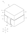
- FIG. 1 is a perspective view showing an example of an inductor according to a first embodiment of the present invention.
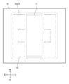
- FIG. 3 is a top view of the inductor according to the first embodiment (however, illustration of the second core is omitted).
- FIG. 2 is a front view of the inductor according to the first embodiment.
- FIG. 3 is a bottom view of the inductor according to the first embodiment.
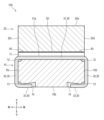
- FIG. 4 is a longitudinal sectional view of the inductor according to the first embodiment taken along the dashed line shown in FIG. 3 and viewed in the direction of the arrow VV.
- FIG. 3 is a top view of the first core in a cutting step in the inductor manufacturing method according to the first embodiment.
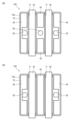
- (a) and (b) are examples of top views of an inductor in which the first core has two grooves (however, the second core is not shown).
- the various components of the inductor of the present invention do not need to exist individually, and multiple components may be formed as a single member, or one component may be formed from a plurality of members. It is allowed that a certain component is a part of another component, that a part of a certain component overlaps with a part of another component, etc.
- the inductor manufacturing method of the present invention may be explained using a plurality of steps described in order, the order of the description does not limit the order or timing of performing the plurality of steps. Therefore, when carrying out the inductor manufacturing method of the present invention, the order of the plurality of steps can be changed within a range that does not affect the content, and some or all of the execution timings of the plurality of steps overlap with each other. You may do so.
- a plane as used in the present invention means a shape physically formed with a plane as a target, and of course does not need to be a geometrically perfect plane.
- terminal portion 33 and the mounting board are joined by solder
- present invention is not limited to this.
- the terminal portion 33 and the mounting board may be joined using not only solder but also other metal solder.
- the inductor 100 includes a first core 10, a conductor 30, a second core 20, a gap material 40, and an adhesive 50.
- the first core 10 is a magnetic material having a groove 11 on the upper surface 10a.
- the conductor 30 is disposed so as to fit into the groove 11 .
- the second core 20 is a magnetic material that is combined with the first core 10 so as to cover the groove portion 11 .
- the gap material 40 is disposed between the first core 10 and the second core 20 to separate the first core 10 and the second core 20 from each other.
- An adhesive 50 is applied between the first core 10 and the second core 20.
- Both ends of the conductor 30 extend from the groove 11 and are respectively arranged along the first and second side surfaces (the front surface 10c and the back surface 10d) of the first core 10 that face each other.
- the distance between the first side surface (front surface 10c or back surface 10d) and the adhesive 50 is the same as the distance between the second side surface (back surface 10d or front surface 10c) and the adhesive 50 when viewed in the extending direction (front-back direction) of the groove 11. Equal to or less than.
- the gap material 40 is disposed between the adhesive 50 and the first side surface (front surface 10c or back surface 10d) when viewed in the extending direction of the groove portion 11.
- the first core 10 and the second core 20 are magnetic bodies that together form a closed magnetic path around the conductor 30.
- the first core 10 and the second core 20 are integrally molded from a magnetic material such as ferrite.
- the first core 10 and the second core 20 have a substantially rectangular parallelepiped shape, and the first core 10 and the second core 20 together have a substantially cubic shape. There is.
- the first core 10 and the second core 20 each have an upper surface (10a, 20a) facing upward, a lower surface (10b, 20b) facing downward, and a front surface (10c, 20c) facing forward, It has a back surface (10d, 20d) facing rearward, a left surface (10e, 20e) facing leftward, and a right surface (10f, 20f) facing rightward.
- the top surface (10a, 20a) and the bottom surface (10b, 20b), the front surface (10c, 20c) and the back surface (10d, 20d), and the left surface (10e, 20e) and right surface (10f, 20f) are opposed to each other. There is.
- the first core 10 and the second core 20 have an upper surface and a lower surface each having a larger area than each of the front surface, back surface, left surface, and right surface, and have a flat shape as a whole.
- the shapes of the first core 10 and the second core 20 are not limited to rectangular parallelepipeds, and may be, for example, prisms with polygonal bottoms.
- the surfaces constituting the first core 10 and the second core 20 do not need to be perfectly flat, and may be curved or distorted.
- the groove portion 11 is a recessed portion formed in the upper surface 10a of the first core 10 so that the conductor 30 fits therein.
- the groove portion 11 is formed as a long groove recessed from the front to the rear in the upper surface 10a of the first core 10.
- the groove portion 11 may be formed in a straight line or may be formed in a curved manner.
- the first core 10 is a U-core having one groove 11 formed on the upper surface 10a, but a plurality of grooves 11 may be formed on the upper surface 10a.
- the first core 10 may be an E-core in which two grooves 11 are formed side by side on the upper surface 10a.
- the groove portion 11 is provided at the center in the width direction of the upper surface 10a, but it may be provided on the left side or right side of the center in the width direction.
- the depth of the groove portion 11 is greater than or equal to the thickness of the fitting portion 31 of the conductor 30, which will be described later.
- the depth of the groove portion 11 and the thickness of the fitting portion 31 of the conductor 30 may be approximately the same, and the top surface 31a of the fitting portion 31 of the conductor 30 and the top surface 10a of the first core 10 may be at the same height.
- the width (length in the width direction) of the groove portion 11 is greater than or equal to the width of the fitting portion 31 of the conductor 30 .
- the width of the groove portion 11 is larger than the width of the conductor 30. Further, as shown in FIG. 3, the conductor 30 is arranged at the center of the groove 11 in the width direction, and a gap is created between the conductor 30 and the groove 11 on both sides of the conductor 30 in the left and right direction. .
- the second core 20 is combined with the first core 10 so as to cover the groove 11
- the second core 20 is combined with the first core 10 so that substantially the entire groove 11 overlaps with the second core 20 when viewed from above. This means that it is placed on the core 10. More specifically, this means that the lower surface 20b of the second core 20 and the groove portion 11 overlap. A part of the groove part 11 does not need to overlap with the second core 20.
- the second core 20 has a shape and dimensions that can cover substantially the entire upper surface 10a of the first core 10 including the groove 11, and when viewed from above, the second core 20 It is placed so that it overlaps with Specifically, the shape and dimensions of the upper surface 10a of the first core 10 and the shape and dimensions of the lower surface 20b of the second core 20 are substantially the same. Furthermore, the front faces (10c, 20c) of the first core 10 and the second core 20, the back faces (10d, 20d), the left faces (10e, 20e), and the right faces (10f, 20f) are on the same plane without any difference in level. The second core 20 is placed on top of the first core 10 so as to be flush with each other.
- the conductor 30 is a member through which current is passed, and is made of a conductive material such as metal.
- the conductor 30 is a generally elongated plate-like member.
- the conductor 30 is arranged along the outer surface of the first core 10 as shown in FIG. Specifically, the intermediate portion of the conductor 30 is fitted into the groove portion 11 of the first core 10 as a fitting portion 31 . Both sides of the fitting part 31 extend from the groove part 11, and the part extending from the groove part 11 is bent with respect to the fitting part 31, and extends along the front surface 10c and the back surface 10d of the first core 10. It is located.
- the portion of the conductor 30 disposed on the front surface 10c and the rear surface 10d of the first core 10 is referred to as an outer surface arrangement portion 32.
- the entire outer surface arrangement portion 32 exists outside the front surface 10c or the back surface 10d of the first core 10.
- the portions of the front surface 10c and back surface 10d of the first core 10 where the outer surface arrangement section 32 extends are formed as recesses, and a part or all of the outer surface arrangement section 32 is formed in the envelope volume of the first core 10. It may also be made to exist within.
- Both ends of the conductor 30 are arranged as terminal parts 33 in the terminal arrangement part 14 provided on the lower surface 10b of the first core 10, and are substantially parallel to the lower surface 10b of the first core 10. That is, the conductor 30 disposed along the front surface 10c or the rear surface 10d is bent toward the lower surface 10b near the boundary between the front surface 10c or the rear surface 10d and the lower surface 10b.
- the terminal portion 33 is a portion of the conductor 30 that is joined to the mounting board by soldering or the like.
- the terminal placement portion 14 is a portion on the lower surface 10b of the first core 10 where the terminal portion 33 of the conductor 30 is placed.
- the first core 10 is formed as an upwardly concave concave portion on the lower surface 10b. As illustrated in FIG.
- the width of the terminal placement portion 14 is greater than or equal to the width of the terminal portion 33
- the length of the terminal placement portion 14 in the front-rear direction is greater than or equal to the length of the terminal portion 33 in the front-rear direction.
- the depth of the recess of the terminal arrangement portion 14 (the length to the bottom of the recess with respect to the lower surface 10b) is smaller in the area closer to the periphery of the lower surface 10b, and larger in the area closer to the center of the lower surface. It has become. That is, the bottom of the concave portion of the terminal arrangement portion 14 is formed in an inclined shape that becomes deeper toward the center of the lower surface 10b.
- the conductor 30 is arranged around the first core 10 in a bent state.
- the terminal portion 33 of the conductor 30 can be placed in a sufficiently bent state so as to bite into the terminal placement portion 14. That is, the terminal portion 33 and the outer surface arrangement portion 32 can be bent so that the angle formed is smaller than 90 degrees. This prevents the terminal portion 33 from floating with respect to the mounting board due to insufficient bending of the terminal portion 33 and the outer surface arrangement portion 32.
- the depth of the shallowest part of the bottom of the recess in the terminal placement part 14 is smaller than the thickness of the terminal part 33.
- the corners that are the boundaries between the groove 11 and the front surface 10c, and between the groove 11 and the rear surface 10d are chamfered, and the upper chamfered portion 12 is preferably formed. Further, it is preferable that the corners that are the boundaries between the terminal placement portion 14 and the front surface 10c and between the terminal placement portion 14 and the back surface 10d are also chamfered to form the lower chamfered portion 13. In this embodiment, the upper chamfered portion 12 and the lower chamfered portion 13 are formed as a step-like chamfered shape.
- the upper chamfered portion 12 and the lower chamfered portion 13 are not limited to the stepped shape described above.
- the upper chamfered portion 12 and the lower chamfered portion 13 may have a C-chamfered shape or an R-chamfered shape.
- the bent portion of the conductor 30 may be in an angular state or may be in an arc shape (R shape).
- R shape arc shape
- the bent portion of the conductor 30 is arc-shaped as in this embodiment, by chamfering the corners of the first core 10 at the positions where the conductor 30 is bent, the sides of the first core 10 and the groove 11 can be The conductor 30 can be in contact with the conductor 30 almost entirely.
- the gap material 40 is a member that separates the upper surface 10a of the first core 10 and the lower surface 20b of the second core 20, as shown in FIG. That is, the gap material 40 separates the first core 10 and the second core 20 so that the distance between the first core 10 and the second core 20 becomes the thickness of the gap material 40.
- the gap material 40 is obtained by cutting the insulating material 60 into a desired shape.
- the insulating material 60 includes a material having insulating properties such as resin, and is formed into a thin sheet having a substantially uniform thickness. By using the insulating material 60 with a predetermined thickness, the gap between the upper surface 10a of the first core 10 and the lower surface 20b of the second core 20 can be adjusted to obtain a desired inductance value.
- the insulating material 60 may be configured by laminating a base material layer and an adhesive layer. For example, in the inductor manufacturing method described below, if the gap material 40 is arranged on the upper surface 10a of the first core 10 so that the adhesive layer is on the first core 10 side, the gap material 40 will be displaced on the upper surface 10a of the first core 10. This can be prevented.
- a tape made of an insulating resin layer such as polyimide coated with an adhesive layer may be used as the insulating material 60.
- a tape having adhesive layers laminated on both sides of a base layer may be used. That is, the gap material 40 and the first core 10 or the second core 20 may be adhered to each other via an adhesive layer.
- the first core 10 and the second core 20 may be bonded together via a gap material 40, and the bonding between the first core 10 and the second core 20 may be assisted by an adhesive 50.
- the gap material 40 is arranged on the upper surface 10a of the first core 10 and the second core 20 is placed so that the gap material 40 is sandwiched between the first core 10, but the present invention is not limited to this.
- the first core 10 may be disposed on the side (lower side) of the gap material 40 disposed on the second core 20.
- the adhesive 50 is a material for bonding the first core 10 and the second core 20 together. That is, the first core 10 and the second core 20 are joined together without being separated by the adhesive 50.
- adhesive resins such as epoxy resins, phenol resins, and acrylic resins can be used.
- the adhesive 50 only needs to be applied in contact with the first core 10 and the second core 20, and may be applied to either the first core 10 or the second core 20 during the manufacturing process. That is, the adhesive 50 may be applied to the first core 10, and the second core 20 may be combined with the side to which the adhesive 50 is applied, or the adhesive 50 may be applied to the second core 20, and the adhesive 50 may be applied to the second core 20.
- the first core 10 may be combined with the coated side.
- the adhesive 50 is sandwiched between the first core 10 and the second core 20 and tends to spread thinly, but even if it spreads thinly, it still has a constant thickness.
- the distance between the first core 10 and the second core 20 can be controlled regardless of the thickness of the adhesive 50. Can be done. Specifically, the distance between the first core 10 and the second core 20 can be the thickness of the gap material 40.
- the first side surface and the second side surface each refer to one of the pair of surfaces (the front surface 10c and the back surface 10d in this embodiment) of the first core 10 along which the conductor 30 is arranged.
- the distance between the adhesive 50 and the first side surface is equal to or shorter than the distance between the adhesive 50 and the second side surface. That is, between the front surface 10c and the back surface 10d, the one that is closer or the same distance from the adhesive 50 is the first side surface, and the other side is the second side surface.
- the adhesive 50 is applied to a region of the upper surface 10a closer to the front surface 10c than the center in the front-rear direction, the first side surface is the front surface 10c, and the second side surface is the rear surface 10d.
- the first side surface is the rear surface 10d
- the second side surface is the front surface 10c.
- any one of the front surface 10c and the rear surface 10d is the first side surface, and the other is the second side surface.
- the adhesive 50 is applied to the center of the upper surface 10a in the front-rear direction, so the first side surface will be described below as the front surface 10c and the second side surface as the back surface 10d.
- the back surface 10d and the second side surface may be the front surface 10c.
- first side surface and the second side surface are defined for each application position of the adhesive 50.
- adhesive 50 (50a, 50b) is applied to the upper surface 10a at one location on each of the left and right regions with the groove 11 in between, and the adhesive 50 is applied at a position from the front surface 10c in the front-rear direction.
- the distance and the distance from the back surface 10d are the same. Therefore, in both the adhesive 50a applied to the left region and the adhesive 50b applied to the right region, the first side surface may be the front surface 10c and the second side surface may be the back surface.
- the first side surface for the adhesive 50a in the left region is the front surface 10c.
- the first side surface of the adhesive 50b in the right side region is the back surface 10d.
- the gap material 40 is disposed in a region (first region 10g) between the adhesive 50 and the first side surface of the adhesive 50 when viewed in the front-rear direction.
- the gap material 40 is disposed in a region (first region 10g) sandwiched between the adhesive 50 and the first side surface in the front-rear direction.
- the adhesive 50 that sandwiches the gap material 40 in the front-rear direction with the first side surface means the main volume portion of the applied adhesive. That is, it refers to the area where the adhesive 50 is dropped onto the first core 10 or the second core 20.
- the adhesive 50 when the adhesive 50 is dropped onto the upper surface 10a of the first core 10 during the manufacturing process of the inductor 100, the adhesive 50 may accidentally scatter. Further, a part of the adhesive 50 that is sandwiched between the first core 10 and the second core 20 and tries to spread laterally crosses over the gap material 40 and becomes between the gap material 40 and the second core 20. Sometimes I get caught up in it unexpectedly. In these cases, the adhesive 50 in the meaning of "the gap material 40 is disposed between the adhesive 50 and the first side surface when viewed in the front-rear direction" refers to the adhesive 50 intentionally applied. This refers to the main volume portion, and does not include the adhesive 50 that accidentally splatters or the adhesive 50 that unexpectedly rides on the gap material 40.
- the adhesive 50 e.g. adhesive 50b
- An upright end surface of the gap material 40 is disposed between the first side surface (front surface 10c) and the first side surface (front surface 10c).
- the adhesive 50 is applied to two places on the top surface 10a (one place on each side with the groove 11 in between), and the adhesive 50 corresponds to each of the two places where the adhesive 50 was applied.
- the gap material 40 is disposed between the first side surface and the first side surface, the present invention is not limited thereto.
- the gap material 40 is disposed between the adhesive 50 and the first side surface at at least one location of the adhesive 50 applied on the upper surface 10a.
- a gap material 40 is disposed between each adhesive 50 and the corresponding first side surface.
- the gap material 40 only needs to be disposed at least in the first region 10g, and may or may not be disposed at other positions on the upper surface 10a.
- the gap material 40 is also arranged in a region between the adhesive 50 and the second side surface (second region 10i) and a third region 10h, which will be described later, when viewed in the front-rear direction, and the gap material 40 is disposed in the groove of the adhesive 50.
- No gap material 40 is arranged on the 11 side. It is not necessary to arrange the gap material 40 in the second region 10i or the third region 10h, and the gap material 40 may be arranged on the groove 11 side of the adhesive 50.
- the gap material 40 is disposed on substantially the entire surface of the first region 10g, but the present invention is not limited to this.
- the gap material 40 may be arranged only on the adhesive 50 side of the first region 10g, or the gap material 40 may be arranged only on the first side surface (front surface 10c) side.
- FIG. 2 only the first region 10g, second region 10i, and third region 10h for the adhesive 50b applied to the right region across the groove 11 on the upper surface 10a are shown.
- the first region 10g, second region 10i and third region 10h of the adhesive 50a applied to the left region sandwich the groove 11 of the first region 10g, second region 10i and third region 10h of the adhesive 50b. exists in a mirror-symmetrical position.
- the adhesive 50 tries to spread radially between the first core 10 and the second core 20 by being sandwiched between the first core 10 and the second core 20.
- the adhesive 50 trying to spread in the extending direction of the conductor 30 is stopped by the gap material 40 disposed in the first region 10g.
- the solder wettability in the outer surface arrangement portion 32 and the terminal portion 33 is maintained well, and a solder fillet is easily formed when bonding to a mounting board by soldering or the like.
- the first core 10 has third and fourth side surfaces (left side 10e and right side 10f in this embodiment) that are arranged in an orthogonal direction (left-right direction) orthogonal to the extending direction (front-back direction) of the groove 11 and are opposed to each other.
- the gap material 40 is further arranged between the adhesive 50 and a third side surface of the third and fourth side surfaces that is close to the adhesive 50 when viewed in the left-right direction.
- a third side surface adjacent to the adhesive 50 is a side surface of the upper surface 10a of the first core 10 in the left-right direction with respect to the adhesive 50, among a pair of side surfaces arranged in the left-right direction and facing each other in the first core 10. These are the sides that are at a distance of less than half the length.
- the third side surface is a side surface disposed on the outside in the width direction on the side opposite to the side where the groove 11 is located when viewed from the adhesive 50
- the fourth side surface is a side surface disposed on the outside in the width direction when viewed from the adhesive 50. This is the side surface located beyond the groove portion 11.
- the third side surface and the fourth side surface are either the left surface 10e or the right surface 10f, respectively.
- the third side surface is the left surface 10e
- the fourth side surface is the right surface 10f.
- the third side surface of the adhesive 50b applied to the region on the right side of the groove portion 11 is the right surface 10f
- the fourth side surface is the left surface 10e.
- the gap material 40 is disposed on the upper surface 10a in a region (third region 10h) between the adhesive 50 and the third side surface when viewed in the left-right direction. In this embodiment, a mode is shown in which the gap material 40 is disposed on substantially the entire surface of the third region 10h, but the present invention is not limited to this.
- the gap material 40 may be arranged only on the adhesive 50 side of the third region 10h, or the gap material 40 may be arranged only on the third side surface side.
- the adhesive 50 that has spread to the opposite side of the groove 11 due to being sandwiched between the first core 10 and the second core 20 is blocked by the gap material 40 disposed in the third region 10h. Thereby, the appearance of the inductor 100 can be kept good without the adhesive 50 leaking to the left or right side of the inductor 100 and causing the appearance of the inductor 100 to deteriorate.
- the gap material 40 disposed between the adhesive 50 and the first side surface and the gap material 40 disposed between the adhesive 50 and the third side surface are continuous. It is formed.
- the gap materials 40 are formed continuously, it does not mean that they are formed as one gap material 40, but also that two gap materials 40 are in contact with each other with an extremely small gap or no gap.
- the gap member 40 may be formed of one member or may be divided into two or more members. For example, one L-shaped gap material 40 is formed, which is disposed astride the first region 10g and the third region 10h.
- the gap material 40 disposed in the first region 10g (for example, the gap material 40g described later) and the gap material 40 disposed in the third region (for example, the gap material 40h described later) come into contact with each other, resulting in an L-shape as a whole. It may be .
- the adhesive 50 leaks to the outer surface of the inductor 100 through the gap. You can prevent it from coming out.
- the gap material 40 is further disposed between the adhesive 50 and the second side surface, and continuously surrounds the adhesive 50 in at least three directions.
- the three directions are the front-rear direction and the opposite side of the groove 11 in the adhesive 50.
- the gap material 40 may also be placed in the area of the adhesive 50 on the groove 11 side, and the entire circumference of the adhesive 50 may be surrounded by the gap material 40, or the gap material 40 may be placed in the area of the adhesive 50 on the groove 11 side. It is not necessary to place .
- the gap material 40 is not disposed at least in a portion of the adhesive 50 on the groove 11 side, and the groove 11 communicates with an enclosing region 10j, which will be described later.
- the adhesive 50 that tends to spread toward the second side surface (back surface 10d) can be dammed up by the gap material 40i. This prevents the adhesive 50 from adhering to the conductor 30 disposed along the second side surface (back surface 10d), and improves the wettability of the terminal portion on the second side surface (back surface 10d) side. can be kept.
- the adhesive 50 that is sandwiched between the first core 10 and the second core 20 and tries to spread can be prevented by the gap material 40. 40, it is dammed in three directions.
- the adhesive 50 leaking from the space surrounded by the gap material 40 spreads toward the groove 11 side, and a portion of the adhesive 50 flows into the groove 11 or onto the conductor 30. This makes it possible to suppress leakage of the adhesive 50 to the outside of the inductor 100 and to prevent the adhesive 50 from leaking over the gap material 40 to the outer surface of the inductor 100. Furthermore, by preventing the adhesive 50 from entering between the gap material 40 and the first core 10 or the second core 20, the gap between the first core 10 and the second core 20 is reduced to the thickness of the adhesive 50. The distance can be controlled to a desired distance without depending on the distance, and the influence on the inductance value can be suppressed.
- the adhesive 50 spreads in the front, back, left and right directions until the thickness of the adhesive 50 becomes equal to or less than the thickness of the gap material 40. That is, the thickness of the adhesive 50 is preferably equal to or less than the thickness of the gap material 40.
- the shape and dimensions of the gap material 40 are such that the volume of the space surrounded by the gap material 40 is larger than the amount of the adhesive 50 to be applied. It is recommended that the
- the gap material 40 has a smaller shape and size than the upper surface 10a of the first core 10. That is, a gap exists between the gap material 40 and the first side surface, the second side surface, the third side surface, or the groove part 11, and there is a distance between them. Since there is a gap between the gap material 40 and the first side surface, the second side surface, or the third side surface, the gap material A space exists on the outer side in the front-rear direction of 40 and on the outer side in the width direction opposite to the groove portion 11.
- the adhesive 50 sandwiched between the first core 10 and the second core 20 unexpectedly enters between the gap material 40 and the first core 10 or the second core 20 and spreads.
- the adhesive 50 can be accommodated in the space. This can better prevent the adhesive 50 from leaking in the front-rear and left-right directions of the inductor 100.
- the joining between the first core 10 and the second core 20 can be confirmed from a front view as shown in FIG.
- the distance L1 between the gap material 40 and the groove portion 11 is smaller than the length in the width direction of the surrounding area 10j, which will be described later. Further, the distance L1 between the gap material 40 and the groove portion 11 is the distance L2 between the gap material 40 and the first side surface, the distance L3 between the gap material 40 and the second side surface, and the distance L3 between the gap material 40 and the third side surface. It is preferable that the length is shorter than or equal to the distance L4.
- the distance L1 between the gap material 40 and the groove portion 11 is smaller than the length L5 in the front-rear direction of the gap material 40 disposed in front or behind the adhesive 50 when viewed in the front-rear direction. Thereby, it is possible to suppress the adhesive 50 from leaking forward or backward of the inductor 100 through the gap between the gap material 40 and the groove portion 11.
- a portion of the adhesive 50 is in contact with a portion of the end surface of the gap material 40.
- the end surface of the gap material 40 is a surface connecting the surface of the gap material 40 that is in contact with the first core 10 and the surface that is in contact with the second core 20, that is, the side surface of the gap material 40. It is sufficient that at least a portion of the adhesive 50 is in contact with at least a portion of the end surface of the gap material 40. In other words, a portion of the adhesive 50 contacts a portion of the end surface of the gap material 40 that faces the adhesive 50 .
- the adhesive 50 when the adhesive 50 is in contact with the end surface of the gap material 40, it means that a portion of the adhesive 50 is in contact with only the end surface of the gap material 40, and that a portion of the adhesive 50 is in contact with the end surface of the gap material 40, and This includes contacting the main surface of the gap material 40. That is, the adhesive 50 may be in contact with the end surface of the gap material 40 and spread between the gap material 40 and the first core 10 or between the gap material 40 and the second core 20.
- the adhesive 50 comes into contact with the end surface of the gap material 40, the adhesive 50 that is sandwiched between the first core 10 and the second core 20 and tends to spread can be stopped by the gap material 40. Further, since the adhesive 50 comes into contact with the end surface of the gap material 40, the space surrounded by the gap material 40 is filled with the adhesive 50, and the volume of the space containing air in the space can be reduced. Thereby, even when the inductor 100 is used in an environment with severe temperature fluctuations, repeated stress loads on the adhesive 50 due to expansion and contraction of the air in the space can be suppressed. As a result, deterioration of the inductor 100 due to long-term use in an environment with severe temperature fluctuations can be suppressed.
- the adhesive 50 may be present on the conductor 30 or inside the groove 11.
- the adhesive 50 dammed by the gap material 40 spreads to the side where the gap material 40 is not disposed (the groove 11 side), and spreads inside the groove 11 and onto the conductor 30. This prevents the adhesive 50 dammed up by the gap material 40 from leaking beyond the gap material 40.
- the groove 11 and the conductor 30 can be fixed to each other.
- the adhesive 50 is applied to the upper surface 10a of the first core 10 on both sides of the groove 11, and a pair of gap materials 40 are applied to extend the groove 11 with the groove 11 in between. They are arranged on both sides of the orthogonal direction (left-right direction).
- the gap material 40 is disposed in the first region 10g of each of the adhesives 50 applied on both sides of the groove 11 in the left-right direction, preferably further in the third region 10h, and more preferably further in the third region 10h. It is arranged in two areas 10i.
- the gap material 40 is formed and arranged with the same symmetry as the adhesive 50 is arranged.
- the gap material 40 is also arranged in mirror-symmetrical positions with respect to the groove 11. It is formed in a mirror-symmetrical shape and is placed in a mirror-symmetrical position. Further, when the adhesive 50 is arranged in a point-symmetrical position with respect to the center point of the upper surface 10a of the first core, the gap material 40 is point-symmetrical with respect to the center point of the upper surface 10a of the first core 10. It is formed into a shape and arranged in point-symmetrical positions.
- the adhesive 50 and the gap material 40 may be applied and arranged on both sides of the groove 11 on the upper surface 10a of the first core 10 when the inductor 100 is provided.
- the adhesive 50 is applied to the lower surface of the second core 20 and the gap material 40 is placed, and when the first core 10 is assembled, the adhesive 50 is applied to both sides of the groove 11.
- the gap material 40 may be applied and the gap material 40 may be placed.
- the adhesive 50 is applied to both sides (the left side and the right side) of at least one of the grooves 11, and the gap material 40 is disposed.
- the adhesive 50 is applied to both sides (the left side and the right side) of at least one of the grooves 11, and the gap material 40 is disposed.
- the adhesive 50 when disposing the gap material 40 or the adhesive 50 in the entire area divided by the groove 11, the adhesive 50 is applied to all three areas divided by the groove 11, as shown in FIG. 7(a). You can.
- the gap material 40 is arranged on both sides of the adhesive 50 in the front-rear direction. Further, in the adhesive 50 applied to the outside in the left-right direction, the gap material 40 is also arranged in a region on the opposite side to the groove portion 11. Alternatively, only the gap material 40 may be placed in the area of the upper surface 10a sandwiched between the two grooves 11, as shown in FIG. 7(b).
- the joining between the first core 10 and the second core 20 can be strengthened. Furthermore, by disposing the gap material 40 in the first region 10g, second region 10i, or third region 10h of the adhesive 50 applied on both sides of the groove 11, each adhesive 50 is exposed to the outside of the inductor 100. It can prevent leakage. Moreover, by arranging the gap material 40 on both sides of the upper surface 10a across the groove 11, the gap between the first core 10 and the second core 20 can be maintained at a desired distance over the entire upper surface 10a.
- the first core 10, second core 20, and gap material 40 can also be provided as a core set that does not include the conductor 30 or the adhesive 50.
- the core set includes a first core 10, a second core 20, and a gap material 40.
- the first core 10 is a magnetic material having the groove 11 on the upper surface 10a
- the second core 20 is a magnetic material used in combination with the first core 10 so as to cover the groove 11.
- the gap material 40 (40g, 40h, 40i) is arranged on the upper surface 10a of the first core 10.
- the gap materials 40 (40g, 40i) are disposed on the upper surface 10a of the first core 10 on both sides of the groove 11 in the extending direction (front-back direction).
- the regions on both sides of the groove portion 11 in the extending direction refer to both one side (front side) and the other side (rear side) with respect to the center of the length of the upper surface 10a in the front-rear direction. That is, at least one gap material 40g is arranged in front of the center of the upper surface 10a in the front-rear direction, and at least one gap material 40i is arranged in the rear. As shown in FIG. 2, the gap material 40g and the gap material 40i have a width that can cover almost the entire width from the third side surface (left surface 10e or right surface 10f) to the groove portion 11. Not limited to.
- the gap material 40g and the gap material 40i only need to cover part of the width from the third side surface to the groove part 11, and do not need to cover part of the width. It is preferable that the gap material 40g disposed on the front side and the gap material 40i disposed on the rear side at least partially overlap when viewed from either one of the extending directions of the groove portion 11. More preferably, the entire gap material 40g disposed on the front side and the entire gap material 40i disposed on the rear side overlap when viewed from either one of the extending directions of the groove portion 11. A part of the area sandwiched between the gap materials 40 arranged on both sides in the front-rear direction is a planned area to which the adhesive 50 is applied (adhesive application planned area 10k). It is desirable that the gap material 40 is fixed to the upper surface 10a of the first core 10. For example, as described above, the gap material 40 having an adhesive layer may be used to attach the gap material 40 to the upper surface 10a of the first core 10.
- the core set is manufactured by arranging the conductor 30 so as to fit into the groove 11 of the first core 10, and applying adhesive 50 to the upper surface 10a of the first core 10 or the lower surface 20b of the second core 20. and the second core 20 are used.
- the adhesive 50 is applied between the first core 10 and the second core 20.
- the adhesive 50 that spreads in the front-rear direction is blocked by the gap material 40g and the gap material 40i.
- the adhesive 50 is prevented from leaking to the front and rear of the inductor 100, the adhesive 50 is difficult to adhere to the conductors 30 disposed on the front surface 10c and the rear surface 10d, and the solder wettability of the conductors 30 is good. is maintained.
- the gap material 40g and the gap material 40i arranged on both sides in the front-rear direction are continuous on the side opposite to the groove 11 in the direction perpendicular to the front-rear direction (left-right direction), and the gap material 40 is arranged in a partial area (surrounding) of the upper surface 10a. It may surround at least three sides of the region 10j). That is, the gap material 40h may be arranged on the side opposite to the groove portion 11 between the gap material 40g and the gap material 40i.
- the surrounding area 10j is an area on the upper surface 10a defined by the gap material 40.
- the gap material 40g, the gap material 40h, and the gap material 40i may be different members, or may be a single member.
- the surrounding area 10j only needs to be surrounded by the gap material 40 on at least three sides in the extending direction of the groove 11 and the opposite side of the groove 11, and even if the groove 11 side is surrounded by the gap material 40, it is not It doesn't have to be.
- Adhesive 50 is applied within the surrounding area 10j. That is, the surrounding area 10j and the adhesive application scheduled area 10k overlap. In this embodiment, substantially the entire adhesive application scheduled area 10k is within the surrounding area 10j, and a part of the adhesive application scheduled area 10k includes the outside of the surrounding area 10j on the groove 11 side. Instead of this embodiment, the entire adhesive application scheduled area 10k may be completely included in the surrounding area 10j. Further, in this embodiment, the center of the adhesive application scheduled area 10k (adhesive application center 10l) exists within the surrounding area 10j. Specifically, the adhesive application center 10l is located at the center of the length of the surrounding area 10j in the front-rear direction.
- the adhesive application center 10l is located closer to the groove portion 11 than the center of the length of the enclosing region 10j in the left-right direction. Specifically, it is located at the center between the groove 11 and the boundary of the surrounding area 10j on the opposite side to the groove 11. Instead of this embodiment, the adhesive application center 10l may be located at the center of the length of the surrounding area 10j in the left-right direction.
- the adhesive 50 By applying the adhesive 50 to the surrounding area 10j, the adhesive 50 that is sandwiched between the first core 10 and the second core 20 and spreads to the opposite side of the groove 11 is blocked by the gap material 40. This can prevent the adhesive 50 from leaking to the outer surface of the inductor 100.
- the inductor 100 manufactured by this method includes the first core 10, the second core 20, the conductor 30, the gap material 40, and the adhesive 50 as described above.
- the first core 10 is a magnetic material having a groove 11 on the upper surface 10a, and the conductor 30 is disposed to fit into the groove 11.
- the second core 20 is a magnetic material that is combined with the first core 10 so as to cover the groove portion 11 .
- the gap material 40 is sandwiched between the first core 10 and the second core 20 to separate the first core 10 and the second core 20 from each other.
- Adhesive 50 joins first core 10 and second core 20 together.
- the method includes a placing step, a cutting step, a removing step, and a bonding step.
- the insulating material 60 is placed so as to cover the upper surface 10a of the first core 10, as shown in FIG.
- the insulating material 60 is a sheet-like material having insulation properties.
- the insulating material 60 may be configured by laminating a base material layer and an adhesive layer as described above, and an example thereof is a tape in which an adhesive layer is coated on an insulating resin layer such as polyimide.
- the adhesive layer is placed in contact with the upper surface 10a of the first core 10, and the insulating material 60 and the first core 10 are fixed. This can prevent the insulating material 60 from shifting from the first core 10 during the cutting process.
- the insulating material 60 may cover at least a portion of the upper surface 10a of the first core 10. Specifically, the insulating material 60 is arranged so as to cover at least the area on the upper surface 10a where the adhesive 50 is to be applied and the periphery thereof. More preferably, the entire area on the left side or right side of the groove 11 of the upper surface 10a is covered, and still more preferably the entire upper surface 10a is covered. Preferably, the insulating material 60 has a shape and dimensions that include the upper surface 10a of the first core 10. Thereby, in the cutting process, the gap materials 40 disposed on both sides of the groove 11 can be cut out at the same time.
- regions of the insulating material 60 on both sides in the extending direction of the groove portion 11 are cut out as the gap material 40 .
- the regions on both sides of the groove 11 in the extending direction refer to any region on the front side and any region on the rear side with respect to the center of the length of the upper surface 10a in the front-rear direction, as described above.
- the insulating material 60 disposed in the front region and the rear region are each cut out as gap material 40 (40g, 40i). It is preferable that the gap material 40g cut out from the front region and the gap material 40i cut out from the rear region at least partially overlap when viewed from either one of the extending directions of the groove portion 11. More preferably, the entire gap material 40g cut out from the front region and the entire gap material 40i cut out from the rear region overlap when viewed from either one of the extending directions of the groove portion 11.
- the gap material 40 is also used in the region connecting the regions on both sides of the groove in the direction in which the groove extends. You can extract it as That is, the gap material 40h may be cut out in a shape that continuously connects the front region and the rear region of the upper surface 10a on the side opposite to the groove portion 11. In this case, the gap material 40 surrounds a partial region of the upper surface 10a in at least three directions.
- a region of the upper surface 10a other than the above-mentioned region may be cut out as the gap material 40.
- a region connecting the front region and the rear region of the upper surface 10a on the groove portion 11 side may also be cut out as the gap material 40.
- Examples of means for cutting out the insulating material 60 include thermal cutting such as laser cutting and physical cutting using a cutting blade.
- the gap material 40 can be cut into a desired shape by irradiating the peripheral edge (dotted chain line in FIG. 6) of the gap material 40 cut out from the insulating material 60 with a laser from above.
- the insulating material 60 excluding the gap material 40 is removed.
- the portion of the insulating material 60 excluding the gap material 40 is continuous. Therefore, the insulating material 60 other than the gap material 40 can be removed from the upper surface 10a at once.
- the gap material 40 It is necessary to remove the outer insulating material 60 and the inner insulating material 60, respectively. Since the portion of the insulating material 60 excluding the gap material 40 is continuous, the portion can be removed at once, and the efficiency of the removal process can be increased.
- the removal step it is preferable to peel off the insulating material 60 in either direction in the extending direction of the groove portion 11.
- the portion of the insulating material 60 excluding the gap material 40 has a protruding portion corresponding to the surrounding area 10j.
- the surrounding area 10j is rectangular.
- the surrounding area 10j may have a shape that becomes narrower outward in the left-right direction.
- the shape may be a semicircle, a trapezoid, or a triangle. Thereby, it is possible to better prevent the protruding portion from being left unpeeled. Further, the flow of the excess adhesive 50 to the groove portion 11 is promoted.
- the conductor 30 is arranged to fit into the groove 11.
- the conductor 30 is bent along the first core 10 and attached to the first core 10.
- the conductor 30 extending from the groove 11 is bent and arranged along the front surface 10c and the rear surface 10d of the first core 10.
- the conductor 30 is bent so that both ends thereof are in contact with the lower surface of the first core 10 and placed in the terminal placement portion 14 of the first core 10 .
- the conductor 30 that has been bent in advance along the first core 10 may be temporarily expanded outward in the extending direction of the fitting portion 31 and then attached to the first core 10 .
- the process of fitting the conductor 30 into the groove and arranging it along the first core 10 may be performed after the removal process or before the placement process.
- adhesive 50 is applied to a position corresponding to the removed portion to join the first core 10 and the second core 20. Specifically, the adhesive 50 is applied to the adhesive application area 10k between the gap material 40 cut out on both sides of the groove 11 in the extending direction. More specifically, an adhesive supply unit such as a nozzle that dispenses the adhesive 50 is arranged above the adhesive application center 10l, and the adhesive 50 is dispensed and applied onto the upper surface 10a of the first core 10. If the region opposite to the groove 11 that connects the gap materials 40 on both sides in the extending direction of the groove 11 is also cut out as the gap material 40, the adhesive 50 is applied to the region of the upper surface 10a surrounded by the gap material 40. . The second core 20 is placed on the first core 10 so as to cover the groove 11, and the first core 10 and the second core 20 are bonded by the adhesive 50 by heating and pressurizing.
- an adhesive supply unit such as a nozzle that dispenses the adhesive 50 is arranged above the adhesive application center 10l, and the adhesive 50 is
- the gap material 40 By cutting out the gap material 40 on both sides of the top surface 10a of the first core 10 in the front-rear direction and applying the adhesive 50 between the gap materials 40, the gap material 40 is sandwiched between the first core 10 and the second core 20 in the joining process.
- the adhesive 50 that spreads is blocked by the gap material 40. This prevents the gap material 40 from leaking forward and backward of the inductor 100, and prevents the adhesive 50 from adhering to the terminal portion 33. This prevents the solder wettability of the terminal portion 33 from deteriorating.
- the gap material 40 can be cut out in accordance with the shape and position of the groove portion 11 of the first core 10. This makes it easy to position the area to be cut out as the gap material 40.
- the area opposite to the groove part 11 that connects the gap materials 40 on both sides in the extending direction of the groove part 11 is also cut out as the gap material 40, and the adhesive 50 is applied to the area surrounded by the gap material 40. This also prevents the liquid from leaking to the surface opposite to the groove portion 11. This better prevents the adhesive 50 from leaking to the outer surface of the inductor 100, and maintains a good appearance of the inductor 100.
- the gap members 40 are arranged on both sides of the upper surface 10a of the first core 10 with the groove 11 in between, that is, on the upper surface 10a excluding the groove 11, but the present invention is not limited to this. I can't do it.
- the gap material 40 may be placed on the conductor 30.
- the gap material 40 may be disposed on the upper surface 31a of the conductor 30.
- the gap members 40 disposed on both sides of the groove portion 11 may be connected to each other on the conductor 30.
- the gap members 40 formed continuously in the first region 10g, the second region 10i, and the third region 10h on both sides of the groove 11 are moved in the extending direction of the groove 11 on the conductor 30. may be connected on both sides. That is, the gap material 40 may be placed on the conductor 30 so as to cross the groove 11 . Thereby, the gap material 40 may be formed to have a hollow rectangular shape that straddles the groove portion 11 as a whole.
- the position where the adhesive 50 is applied is not limited to the upper surface 10a of the first core 10.
- the adhesive 50 may be applied to the upper surface 31a of the conductor 30.
- the adhesive 50 may be applied to the upper surface 31a of the conductor 30.
- the adhesive 50 may be applied discretely to each area on the upper surface 31a of the first core 10 on both sides of the conductor 30 in the left-right direction and to the area above the conductor 30, and the adhesive 50 may be applied across the conductor 30 in the left-right direction.
- the adhesive may be applied in a linear manner.
- the adhesive 50 is applied to the upper surface 10a of the conductor 30, it is preferable that gap members 40 are also disposed on both sides of the adhesive 50 on the upper surface 31a of the conductor 30 in the direction in which the groove 11 extends. Further, if the upper surface 31a of the conductor 30 and the upper surface 10a of the first core 10 are flush with each other, or the upper surface 31a of the conductor 30 is at approximately the same height as the upper surface 10a of the first core 10. In this case, the adhesive 50 may be applied only on the conductor 30 and the gap material 40 may be placed.
- the adhesive 50 is applied to each of the upper surface 10a of the first core 10 at one location on both sides of the groove 11, but the present invention is not limited thereto.
- the adhesive 50 may be applied to two or more locations in one region of the upper surface 10a with the groove 11 interposed therebetween. That is, the adhesive 50 may be applied to a plurality of positions in each region on both sides of the groove 11 on the upper surface 10a, and the gap material 40 may be arranged. In that case, it is sufficient that the gap material 40 is disposed in the first region 10g of the adhesive 50 applied to at least one place, and the gap material 40 is disposed in the first region 10g of all the adhesives 50. preferable.
- the first side surface does not necessarily refer to the same side surface.
- the first side surface of the adhesive 50 applied to the front side is the front surface 10c
- the first side surface of the adhesive 50 applied to the rear side is the front side 10c.
- the first side is the back surface 10d.
- the insulating material 60 is mainly made of a laminated adhesive layer and a base material layer, but the gap material 40 may be formed from the insulating material 60 without an adhesive layer.
- the first core 10 and the insulating material 60 are each not shown. It may be fixed to a holding jig to prevent the first core 10 and the insulating material 60 from shifting.
- the adhesive 50 comes into contact with the end surface of the gap material 40, so that the first core 10, the second core 20, and the gap material 40 are bonded together. can be fixed to each other.
- the conductor 30 is entirely a plate-shaped member, but the present invention is not limited to this.
- the terminal portions 33 at both ends of the conductor 30 may have a planar shape, and the middle of the conductor 30 may be a wire.
- both ends of the conductor 30 are composed of a terminal portion 33 disposed on the lower surface 20b of the first core 10 and an upright portion disposed vertically on the side surface of the inductor 100.
- the wire is wound around the magnetic legs of the core. Both ends of the wire may be tied to a binding terminal electrically connected to the upright portion, and the wire and the terminal portion 33 may be electrically connected.
- a first core that is a magnetic material having a groove on its upper surface, a conductor disposed to fit into the groove, and a second core that is a magnetic material that is combined with the first core so as to cover the groove.
- a core a gap material disposed between the first core and the second core to separate the first core and the second core, and applied between the first core and the second core.
- an adhesive wherein both ends of the conductor extend from the groove and are respectively disposed along mutually opposing first and second side surfaces of the first core, and the conductor has an adhesive extending from the groove.
- the distance between the first side surface and the adhesive when viewed in the extending direction is equal to or smaller than the distance between the second side surface and the adhesive, and the gap material is the distance between the adhesive when viewed in the extending direction. and the first side surface.
- the first core has third and fourth side surfaces disposed in an orthogonal direction perpendicular to the extending direction and facing each other, and the gap material has the adhesive when viewed in the orthogonal direction. and the third side surface that is close to the adhesive among the third and fourth side surfaces, the inductor according to (1).
- the gap material disposed between the adhesive and the first side surface and the gap material disposed between the adhesive and the third side surface are formed in a continuous manner. The inductor according to (2).
- a core set comprising: a gap material disposed on the top surface, and the gap material being disposed on both sides of the groove in the extending direction.
- the gap materials disposed on both sides of the extending direction are continuous on a side opposite to the groove in a direction perpendicular to the extending direction, and the gap materials are arranged on at least three sides of a partial area of the upper surface.
- a first core having a groove on its upper surface; a conductor disposed to fit into the groove; a second core combined with the first core so as to cover the groove; and a first core.
- Manufacturing an inductor comprising: a gap material that is sandwiched between the second core and separates the first core and the second core; and an adhesive that joins the first core and the second core.
- the method includes an arrangement step in which an insulating material is arranged on the first core so as to cover the upper surface, and a cutting step in which regions of the insulating material on both sides in the extending direction of the groove are cut out as gap material.
- Bonding process and inductor manufacturing method including. (10) In the cutting step, a region of the insulating material that connects the regions on both sides on the side opposite to the groove in a direction orthogonal to the extending direction is also cut out as the gap material.
- a method of manufacturing an inductor is also cut out as the gap material.
Landscapes
- Engineering & Computer Science (AREA)
- Power Engineering (AREA)
- Microelectronics & Electronic Packaging (AREA)
- Manufacturing & Machinery (AREA)
- Coils Or Transformers For Communication (AREA)
Priority Applications (3)
| Application Number | Priority Date | Filing Date | Title |
|---|---|---|---|
| JP2024531804A JPWO2024009405A1 (https=) | 2022-07-05 | 2022-07-05 | |
| CN202280096009.XA CN119173966A (zh) | 2022-07-05 | 2022-07-05 | 电感器、芯组件和电感器制造方法 |
| PCT/JP2022/026734 WO2024009405A1 (ja) | 2022-07-05 | 2022-07-05 | インダクタ、コアセットおよびインダクタ製造方法 |
Applications Claiming Priority (1)
| Application Number | Priority Date | Filing Date | Title |
|---|---|---|---|
| PCT/JP2022/026734 WO2024009405A1 (ja) | 2022-07-05 | 2022-07-05 | インダクタ、コアセットおよびインダクタ製造方法 |
Publications (1)
| Publication Number | Publication Date |
|---|---|
| WO2024009405A1 true WO2024009405A1 (ja) | 2024-01-11 |
Family
ID=89453023
Family Applications (1)
| Application Number | Title | Priority Date | Filing Date |
|---|---|---|---|
| PCT/JP2022/026734 Ceased WO2024009405A1 (ja) | 2022-07-05 | 2022-07-05 | インダクタ、コアセットおよびインダクタ製造方法 |
Country Status (3)
| Country | Link |
|---|---|
| JP (1) | JPWO2024009405A1 (https=) |
| CN (1) | CN119173966A (https=) |
| WO (1) | WO2024009405A1 (https=) |
Citations (5)
| Publication number | Priority date | Publication date | Assignee | Title |
|---|---|---|---|---|
| JPH01199415A (ja) * | 1988-02-04 | 1989-08-10 | Matsushita Electric Ind Co Ltd | インダクタンス素子及びその製造方法 |
| JP2000315610A (ja) * | 1999-04-28 | 2000-11-14 | Tokin Corp | チョークコイル |
| JP2006294830A (ja) * | 2005-04-11 | 2006-10-26 | Sumitomo Electric Ind Ltd | コア及びリアクトル |
| JP2008021836A (ja) * | 2006-07-13 | 2008-01-31 | Mitsubishi Electric Corp | 電磁デバイス |
| CN207651307U (zh) * | 2017-11-30 | 2018-07-24 | 东莞市华昕电子有限公司 | K系数变压器改进结构 |
Family Cites Families (4)
| Publication number | Priority date | Publication date | Assignee | Title |
|---|---|---|---|---|
| JPS549818U (https=) * | 1977-06-23 | 1979-01-23 | ||
| JPH0319306A (ja) * | 1989-06-16 | 1991-01-28 | Tokyo Electric Co Ltd | 電磁装置 |
| CN105185531A (zh) * | 2015-09-14 | 2015-12-23 | 广东新昇电业科技股份有限公司 | 一种新型电抗器铁芯结构及其生产工艺 |
| JP2020021770A (ja) * | 2018-07-30 | 2020-02-06 | Njコンポーネント株式会社 | コイル部品 |
-
2022
- 2022-07-05 JP JP2024531804A patent/JPWO2024009405A1/ja active Pending
- 2022-07-05 WO PCT/JP2022/026734 patent/WO2024009405A1/ja not_active Ceased
- 2022-07-05 CN CN202280096009.XA patent/CN119173966A/zh active Pending
Patent Citations (5)
| Publication number | Priority date | Publication date | Assignee | Title |
|---|---|---|---|---|
| JPH01199415A (ja) * | 1988-02-04 | 1989-08-10 | Matsushita Electric Ind Co Ltd | インダクタンス素子及びその製造方法 |
| JP2000315610A (ja) * | 1999-04-28 | 2000-11-14 | Tokin Corp | チョークコイル |
| JP2006294830A (ja) * | 2005-04-11 | 2006-10-26 | Sumitomo Electric Ind Ltd | コア及びリアクトル |
| JP2008021836A (ja) * | 2006-07-13 | 2008-01-31 | Mitsubishi Electric Corp | 電磁デバイス |
| CN207651307U (zh) * | 2017-11-30 | 2018-07-24 | 东莞市华昕电子有限公司 | K系数变压器改进结构 |
Also Published As
| Publication number | Publication date |
|---|---|
| JPWO2024009405A1 (https=) | 2024-01-11 |
| CN119173966A (zh) | 2024-12-20 |
Similar Documents
| Publication | Publication Date | Title |
|---|---|---|
| US11304308B2 (en) | Flexible circuit board interconnection and methods | |
| US11462347B2 (en) | Coil component and method of manufacturing coil component | |
| JP6303341B2 (ja) | コイル部品 | |
| JP7816933B2 (ja) | コイル装置 | |
| TW201342403A (zh) | 線圈零件 | |
| US11664145B2 (en) | Inductor | |
| JP2026032156A (ja) | コイル装置 | |
| WO2024009405A1 (ja) | インダクタ、コアセットおよびインダクタ製造方法 | |
| CN208258175U (zh) | 双面柔性印刷电路组件及用于热压熔锡焊接柔性印刷电路组件的系统 | |
| JP2015084405A (ja) | コイル装置 | |
| JP2025014451A (ja) | コイル装置 | |
| JP2012081481A (ja) | 電子部品における電極の接続構造 | |
| JP7510826B2 (ja) | コイル装置 | |
| JPH06283836A (ja) | プリント基板の接続構造および接続方法 | |
| KR20180069943A (ko) | 양면냉각 파워모듈 및 그 제조방법 | |
| US7009142B2 (en) | System and method for joining flat flexible cables | |
| JP2022043352A (ja) | コイル部品 | |
| JP7569643B2 (ja) | コイル装置 | |
| WO2024100792A1 (ja) | インダクタ | |
| JPH10107513A (ja) | 非可逆回路素子及びその電気部品の接続方法 | |
| JP4747667B2 (ja) | 巻線型コイル部品 | |
| KR101197036B1 (ko) | 온도휴즈 | |
| JP3445072B2 (ja) | シートトランス | |
| JP2524131Y2 (ja) | 導波管型終端器 | |
| JPH04326783A (ja) | 半導体レーザ装置用ステムの製造方法 |
Legal Events
| Date | Code | Title | Description |
|---|---|---|---|
| 121 | Ep: the epo has been informed by wipo that ep was designated in this application |
Ref document number: 22950199 Country of ref document: EP Kind code of ref document: A1 |
|
| WWE | Wipo information: entry into national phase |
Ref document number: 2024531804 Country of ref document: JP |
|
| NENP | Non-entry into the national phase |
Ref country code: DE |
|
| 122 | Ep: pct application non-entry in european phase |
Ref document number: 22950199 Country of ref document: EP Kind code of ref document: A1 |