WO2024009405A1 - Inductor, core set, and method for manufacturing inductor - Google Patents
Inductor, core set, and method for manufacturing inductor Download PDFInfo
- Publication number
- WO2024009405A1 WO2024009405A1 PCT/JP2022/026734 JP2022026734W WO2024009405A1 WO 2024009405 A1 WO2024009405 A1 WO 2024009405A1 JP 2022026734 W JP2022026734 W JP 2022026734W WO 2024009405 A1 WO2024009405 A1 WO 2024009405A1
- Authority
- WO
- WIPO (PCT)
- Prior art keywords
- core
- adhesive
- groove
- gap material
- gap
- Prior art date
Links
- 238000000034 method Methods 0.000 title claims description 25
- 238000004519 manufacturing process Methods 0.000 title claims description 23
- 239000000463 material Substances 0.000 claims abstract description 271
- 239000000853 adhesive Substances 0.000 claims abstract description 250
- 230000001070 adhesive effect Effects 0.000 claims abstract description 250
- 239000004020 conductor Substances 0.000 claims abstract description 101
- 239000011810 insulating material Substances 0.000 claims description 48
- 239000000696 magnetic material Substances 0.000 claims description 21
- 238000005520 cutting process Methods 0.000 claims description 19
- 238000005304 joining Methods 0.000 claims description 10
- 238000004026 adhesive bonding Methods 0.000 claims 1
- 229910000679 solder Inorganic materials 0.000 description 19
- 239000012790 adhesive layer Substances 0.000 description 14
- 239000010410 layer Substances 0.000 description 8
- 238000005476 soldering Methods 0.000 description 4
- 239000002184 metal Substances 0.000 description 3
- 239000011347 resin Substances 0.000 description 3
- 229920005989 resin Polymers 0.000 description 3
- 239000004642 Polyimide Substances 0.000 description 2
- 238000010030 laminating Methods 0.000 description 2
- 229920001721 polyimide Polymers 0.000 description 2
- 239000004925 Acrylic resin Substances 0.000 description 1
- 229920000178 Acrylic resin Polymers 0.000 description 1
- 239000004840 adhesive resin Substances 0.000 description 1
- 229920006223 adhesive resin Polymers 0.000 description 1
- 238000005452 bending Methods 0.000 description 1
- 239000007767 bonding agent Substances 0.000 description 1
- 238000005219 brazing Methods 0.000 description 1
- 239000000470 constituent Substances 0.000 description 1
- 230000008602 contraction Effects 0.000 description 1
- 230000006866 deterioration Effects 0.000 description 1
- 230000002542 deteriorative effect Effects 0.000 description 1
- 238000005516 engineering process Methods 0.000 description 1
- 239000003822 epoxy resin Substances 0.000 description 1
- 238000007667 floating Methods 0.000 description 1
- LNEPOXFFQSENCJ-UHFFFAOYSA-N haloperidol Chemical compound C1CC(O)(C=2C=CC(Cl)=CC=2)CCN1CCCC(=O)C1=CC=C(F)C=C1 LNEPOXFFQSENCJ-UHFFFAOYSA-N 0.000 description 1
- 238000010438 heat treatment Methods 0.000 description 1
- 238000009413 insulation Methods 0.000 description 1
- 230000001678 irradiating effect Effects 0.000 description 1
- 238000003698 laser cutting Methods 0.000 description 1
- 239000007788 liquid Substances 0.000 description 1
- 230000007774 longterm Effects 0.000 description 1
- 238000012986 modification Methods 0.000 description 1
- 230000004048 modification Effects 0.000 description 1
- 230000002093 peripheral effect Effects 0.000 description 1
- 239000005011 phenolic resin Substances 0.000 description 1
- 229920000647 polyepoxide Polymers 0.000 description 1
- 229910000859 α-Fe Inorganic materials 0.000 description 1
Images


Classifications
-
- H—ELECTRICITY
- H01—ELECTRIC ELEMENTS
- H01F—MAGNETS; INDUCTANCES; TRANSFORMERS; SELECTION OF MATERIALS FOR THEIR MAGNETIC PROPERTIES
- H01F17/00—Fixed inductances of the signal type
- H01F17/04—Fixed inductances of the signal type with magnetic core
- H01F17/06—Fixed inductances of the signal type with magnetic core with core substantially closed in itself, e.g. toroid
-
- H—ELECTRICITY
- H01—ELECTRIC ELEMENTS
- H01F—MAGNETS; INDUCTANCES; TRANSFORMERS; SELECTION OF MATERIALS FOR THEIR MAGNETIC PROPERTIES
- H01F27/00—Details of transformers or inductances, in general
- H01F27/24—Magnetic cores
-
- H—ELECTRICITY
- H01—ELECTRIC ELEMENTS
- H01F—MAGNETS; INDUCTANCES; TRANSFORMERS; SELECTION OF MATERIALS FOR THEIR MAGNETIC PROPERTIES
- H01F41/00—Apparatus or processes specially adapted for manufacturing or assembling magnets, inductances or transformers; Apparatus or processes specially adapted for manufacturing materials characterised by their magnetic properties
- H01F41/02—Apparatus or processes specially adapted for manufacturing or assembling magnets, inductances or transformers; Apparatus or processes specially adapted for manufacturing materials characterised by their magnetic properties for manufacturing cores, coils, or magnets
Definitions
- the present invention relates to an inductor, a core set that constitutes such an inductor, and a method of manufacturing such an inductor.
- Some inductors have a plurality of magnetic cores surrounding a conductor and a gap material placed between the magnetic cores to provide a gap between the magnetic cores. Specifically, a conductor is fitted into a groove formed on the top surface of a U-shaped core or an E-shaped core, a gap material is placed on the top surface, and the gap material is connected to a U-shaped core or an E-shaped core. There is an inductor in which an I-shaped core is further placed between the core and the I-shaped core. The U-shaped core or the E-shaped core is bonded to the I-shaped core using an adhesive or the like.
- the conductor (2) is arranged so as to fit into the central groove of the U-shaped magnetic core (1b).
- the conductor (2) is integrally formed with a gap material (6), and the gap material (6) is provided in the middle of the length of the conductor (2) in the extending direction, and is orthogonal to the conductor (2). It is formed like this.
- the adhesive (4) is applied to the four corners of the upper surface of the U-shaped magnetic core (1b) where the grooves are provided. That is, the gap material (6) is arranged on the inside in the extending direction of the conductor (2) when viewed from the adhesive (4).
- the I-type magnetic core (1a) is placed on top of the U-type magnetic core (1b), and is pressurized and heat-cured to form the I-type magnetic core (1a), the U-type magnetic core (1b), and the gap material ( 6) are each fixed.
- Both ends of the conductor (2) extend from the groove and are bent along the outer surface of the U-shaped magnetic core (1b) to become mounting terminals. Specifically, both ends of the conductor (2) are each bent twice to form an upright portion along the side surface of the U-shaped magnetic core (1b) and a flat portion along the lower surface of the U-shaped magnetic core (1b). A mounting terminal is formed.
- a mounting terminal of the inductor and a mounting board are bonded together using a conductive bonding agent such as solder.
- solder When the mounting terminal has an upright portion and a flat portion as in the inductor of Patent Document 1, in addition to solder joining the opposing flat portion and the mounting board, solder also rises on the upright portion along the side surface of the inductor.
- a triangular prism-shaped (triangular shape in side view) solder fillet is formed between the solder fillet and the mounting board.
- the surface of the mounting terminal of the inductor has good solder wettability.
- solder wettability is good, when the mounting terminal and the mounting board are soldered together, the solder will sufficiently rise and extend along the raised portion of the mounting terminal, and a solder fillet will be formed in the desired size and shape. It's for a reason. If the solder fillet is well formed, the bond between the mounting terminal and the mounting board will be strong, and the conductivity between the mounting terminal and the mounting board will also be good.
- the adhesive When configuring an inductor as in Patent Document 1, when the I-type magnetic core (1a) is placed on the U-type magnetic core (1b), the adhesive (4) connects the U-type magnetic core (1b) and the I-type magnetic core.
- the present invention has been made in view of the above-mentioned problems, and provides an inductor with good wettability on the terminal surface.
- the inductor of the present invention includes a first core made of a magnetic material having a groove on its upper surface, a conductor disposed to fit into the groove, and a magnetic material combined with the first core so as to cover the groove. a second core; a gap material disposed between the first core and the second core to separate the first core and the second core; and a gap material between the first core and the second core.
- both ends of the conductor extending from the groove and being respectively disposed along mutually opposing first and second side surfaces of the first core;
- the distance between the first side surface and the adhesive when viewed in the extending direction of the groove is equal to or smaller than the distance between the second side surface and the adhesive, and the gap material is It is characterized in that it is disposed between the adhesive and the first side surface.
- the core set of the present invention includes a first core that is a magnetic material having a groove on its upper surface, a second core that is a magnetic material that is used in combination with the first core so as to cover the groove, and a second core that is a magnetic material that is used in combination with the first core so as to cover the groove. and a gap material disposed on the upper surface, and the gap material is disposed on both sides of the groove in the extending direction of the groove.
- the method for manufacturing an inductor of the present invention includes: a first core having a groove on its upper surface; a conductor disposed to fit into the groove; and a second core combined with the first core so as to cover the groove. , a gap material that is sandwiched between the first core and the second core to separate the first core and the second core; and an adhesive that joins the first core and the second core.
- a method for manufacturing an inductor comprising: an arrangement step in which an insulating material is arranged on the first core so as to cover the upper surface; and regions of the insulating material on both sides in the extending direction of the groove are gap materials.
- a cutting step in which a portion of the insulating material excluding the gap material is removed; and a removal step in which the adhesive is applied to a position corresponding to the removed portion to separate the first core and the first core. and a joining step of joining the two cores.
- the adhesive that is sandwiched between the first core and the second core and tries to spread in the extending direction of the conductor is stopped by the gap material. This prevents the adhesive from leaking to the side surface of the first core along which both ends of the conductor lie, and maintains good wettability on the surface of the mounting terminal.
- the inductor, core set, and inductor manufacturing method of the present invention it is possible to provide an inductor with good terminal surface wettability.
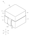
- FIG. 1 is a perspective view showing an example of an inductor according to a first embodiment of the present invention.
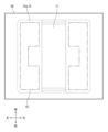
- FIG. 3 is a top view of the inductor according to the first embodiment (however, illustration of the second core is omitted).
- FIG. 2 is a front view of the inductor according to the first embodiment.
- FIG. 3 is a bottom view of the inductor according to the first embodiment.
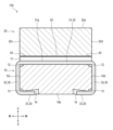
- FIG. 4 is a longitudinal sectional view of the inductor according to the first embodiment taken along the dashed line shown in FIG. 3 and viewed in the direction of the arrow VV.
- FIG. 3 is a top view of the first core in a cutting step in the inductor manufacturing method according to the first embodiment.
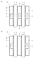
- (a) and (b) are examples of top views of an inductor in which the first core has two grooves (however, the second core is not shown).
- the various components of the inductor of the present invention do not need to exist individually, and multiple components may be formed as a single member, or one component may be formed from a plurality of members. It is allowed that a certain component is a part of another component, that a part of a certain component overlaps with a part of another component, etc.
- the inductor manufacturing method of the present invention may be explained using a plurality of steps described in order, the order of the description does not limit the order or timing of performing the plurality of steps. Therefore, when carrying out the inductor manufacturing method of the present invention, the order of the plurality of steps can be changed within a range that does not affect the content, and some or all of the execution timings of the plurality of steps overlap with each other. You may do so.
- a plane as used in the present invention means a shape physically formed with a plane as a target, and of course does not need to be a geometrically perfect plane.
- terminal portion 33 and the mounting board are joined by solder
- present invention is not limited to this.
- the terminal portion 33 and the mounting board may be joined using not only solder but also other metal solder.
- the inductor 100 includes a first core 10, a conductor 30, a second core 20, a gap material 40, and an adhesive 50.
- the first core 10 is a magnetic material having a groove 11 on the upper surface 10a.
- the conductor 30 is disposed so as to fit into the groove 11 .
- the second core 20 is a magnetic material that is combined with the first core 10 so as to cover the groove portion 11 .
- the gap material 40 is disposed between the first core 10 and the second core 20 to separate the first core 10 and the second core 20 from each other.
- An adhesive 50 is applied between the first core 10 and the second core 20.
- Both ends of the conductor 30 extend from the groove 11 and are respectively arranged along the first and second side surfaces (the front surface 10c and the back surface 10d) of the first core 10 that face each other.
- the distance between the first side surface (front surface 10c or back surface 10d) and the adhesive 50 is the same as the distance between the second side surface (back surface 10d or front surface 10c) and the adhesive 50 when viewed in the extending direction (front-back direction) of the groove 11. Equal to or less than.
- the gap material 40 is disposed between the adhesive 50 and the first side surface (front surface 10c or back surface 10d) when viewed in the extending direction of the groove portion 11.
- the first core 10 and the second core 20 are magnetic bodies that together form a closed magnetic path around the conductor 30.
- the first core 10 and the second core 20 are integrally molded from a magnetic material such as ferrite.
- the first core 10 and the second core 20 have a substantially rectangular parallelepiped shape, and the first core 10 and the second core 20 together have a substantially cubic shape. There is.
- the first core 10 and the second core 20 each have an upper surface (10a, 20a) facing upward, a lower surface (10b, 20b) facing downward, and a front surface (10c, 20c) facing forward, It has a back surface (10d, 20d) facing rearward, a left surface (10e, 20e) facing leftward, and a right surface (10f, 20f) facing rightward.
- the top surface (10a, 20a) and the bottom surface (10b, 20b), the front surface (10c, 20c) and the back surface (10d, 20d), and the left surface (10e, 20e) and right surface (10f, 20f) are opposed to each other. There is.
- the first core 10 and the second core 20 have an upper surface and a lower surface each having a larger area than each of the front surface, back surface, left surface, and right surface, and have a flat shape as a whole.
- the shapes of the first core 10 and the second core 20 are not limited to rectangular parallelepipeds, and may be, for example, prisms with polygonal bottoms.
- the surfaces constituting the first core 10 and the second core 20 do not need to be perfectly flat, and may be curved or distorted.
- the groove portion 11 is a recessed portion formed in the upper surface 10a of the first core 10 so that the conductor 30 fits therein.
- the groove portion 11 is formed as a long groove recessed from the front to the rear in the upper surface 10a of the first core 10.
- the groove portion 11 may be formed in a straight line or may be formed in a curved manner.
- the first core 10 is a U-core having one groove 11 formed on the upper surface 10a, but a plurality of grooves 11 may be formed on the upper surface 10a.
- the first core 10 may be an E-core in which two grooves 11 are formed side by side on the upper surface 10a.
- the groove portion 11 is provided at the center in the width direction of the upper surface 10a, but it may be provided on the left side or right side of the center in the width direction.
- the depth of the groove portion 11 is greater than or equal to the thickness of the fitting portion 31 of the conductor 30, which will be described later.
- the depth of the groove portion 11 and the thickness of the fitting portion 31 of the conductor 30 may be approximately the same, and the top surface 31a of the fitting portion 31 of the conductor 30 and the top surface 10a of the first core 10 may be at the same height.
- the width (length in the width direction) of the groove portion 11 is greater than or equal to the width of the fitting portion 31 of the conductor 30 .
- the width of the groove portion 11 is larger than the width of the conductor 30. Further, as shown in FIG. 3, the conductor 30 is arranged at the center of the groove 11 in the width direction, and a gap is created between the conductor 30 and the groove 11 on both sides of the conductor 30 in the left and right direction. .
- the second core 20 is combined with the first core 10 so as to cover the groove 11
- the second core 20 is combined with the first core 10 so that substantially the entire groove 11 overlaps with the second core 20 when viewed from above. This means that it is placed on the core 10. More specifically, this means that the lower surface 20b of the second core 20 and the groove portion 11 overlap. A part of the groove part 11 does not need to overlap with the second core 20.
- the second core 20 has a shape and dimensions that can cover substantially the entire upper surface 10a of the first core 10 including the groove 11, and when viewed from above, the second core 20 It is placed so that it overlaps with Specifically, the shape and dimensions of the upper surface 10a of the first core 10 and the shape and dimensions of the lower surface 20b of the second core 20 are substantially the same. Furthermore, the front faces (10c, 20c) of the first core 10 and the second core 20, the back faces (10d, 20d), the left faces (10e, 20e), and the right faces (10f, 20f) are on the same plane without any difference in level. The second core 20 is placed on top of the first core 10 so as to be flush with each other.
- the conductor 30 is a member through which current is passed, and is made of a conductive material such as metal.
- the conductor 30 is a generally elongated plate-like member.
- the conductor 30 is arranged along the outer surface of the first core 10 as shown in FIG. Specifically, the intermediate portion of the conductor 30 is fitted into the groove portion 11 of the first core 10 as a fitting portion 31 . Both sides of the fitting part 31 extend from the groove part 11, and the part extending from the groove part 11 is bent with respect to the fitting part 31, and extends along the front surface 10c and the back surface 10d of the first core 10. It is located.
- the portion of the conductor 30 disposed on the front surface 10c and the rear surface 10d of the first core 10 is referred to as an outer surface arrangement portion 32.
- the entire outer surface arrangement portion 32 exists outside the front surface 10c or the back surface 10d of the first core 10.
- the portions of the front surface 10c and back surface 10d of the first core 10 where the outer surface arrangement section 32 extends are formed as recesses, and a part or all of the outer surface arrangement section 32 is formed in the envelope volume of the first core 10. It may also be made to exist within.
- Both ends of the conductor 30 are arranged as terminal parts 33 in the terminal arrangement part 14 provided on the lower surface 10b of the first core 10, and are substantially parallel to the lower surface 10b of the first core 10. That is, the conductor 30 disposed along the front surface 10c or the rear surface 10d is bent toward the lower surface 10b near the boundary between the front surface 10c or the rear surface 10d and the lower surface 10b.
- the terminal portion 33 is a portion of the conductor 30 that is joined to the mounting board by soldering or the like.
- the terminal placement portion 14 is a portion on the lower surface 10b of the first core 10 where the terminal portion 33 of the conductor 30 is placed.
- the first core 10 is formed as an upwardly concave concave portion on the lower surface 10b. As illustrated in FIG.
- the width of the terminal placement portion 14 is greater than or equal to the width of the terminal portion 33
- the length of the terminal placement portion 14 in the front-rear direction is greater than or equal to the length of the terminal portion 33 in the front-rear direction.
- the depth of the recess of the terminal arrangement portion 14 (the length to the bottom of the recess with respect to the lower surface 10b) is smaller in the area closer to the periphery of the lower surface 10b, and larger in the area closer to the center of the lower surface. It has become. That is, the bottom of the concave portion of the terminal arrangement portion 14 is formed in an inclined shape that becomes deeper toward the center of the lower surface 10b.
- the conductor 30 is arranged around the first core 10 in a bent state.
- the terminal portion 33 of the conductor 30 can be placed in a sufficiently bent state so as to bite into the terminal placement portion 14. That is, the terminal portion 33 and the outer surface arrangement portion 32 can be bent so that the angle formed is smaller than 90 degrees. This prevents the terminal portion 33 from floating with respect to the mounting board due to insufficient bending of the terminal portion 33 and the outer surface arrangement portion 32.
- the depth of the shallowest part of the bottom of the recess in the terminal placement part 14 is smaller than the thickness of the terminal part 33.
- the corners that are the boundaries between the groove 11 and the front surface 10c, and between the groove 11 and the rear surface 10d are chamfered, and the upper chamfered portion 12 is preferably formed. Further, it is preferable that the corners that are the boundaries between the terminal placement portion 14 and the front surface 10c and between the terminal placement portion 14 and the back surface 10d are also chamfered to form the lower chamfered portion 13. In this embodiment, the upper chamfered portion 12 and the lower chamfered portion 13 are formed as a step-like chamfered shape.
- the upper chamfered portion 12 and the lower chamfered portion 13 are not limited to the stepped shape described above.
- the upper chamfered portion 12 and the lower chamfered portion 13 may have a C-chamfered shape or an R-chamfered shape.
- the bent portion of the conductor 30 may be in an angular state or may be in an arc shape (R shape).
- R shape arc shape
- the bent portion of the conductor 30 is arc-shaped as in this embodiment, by chamfering the corners of the first core 10 at the positions where the conductor 30 is bent, the sides of the first core 10 and the groove 11 can be The conductor 30 can be in contact with the conductor 30 almost entirely.
- the gap material 40 is a member that separates the upper surface 10a of the first core 10 and the lower surface 20b of the second core 20, as shown in FIG. That is, the gap material 40 separates the first core 10 and the second core 20 so that the distance between the first core 10 and the second core 20 becomes the thickness of the gap material 40.
- the gap material 40 is obtained by cutting the insulating material 60 into a desired shape.
- the insulating material 60 includes a material having insulating properties such as resin, and is formed into a thin sheet having a substantially uniform thickness. By using the insulating material 60 with a predetermined thickness, the gap between the upper surface 10a of the first core 10 and the lower surface 20b of the second core 20 can be adjusted to obtain a desired inductance value.
- the insulating material 60 may be configured by laminating a base material layer and an adhesive layer. For example, in the inductor manufacturing method described below, if the gap material 40 is arranged on the upper surface 10a of the first core 10 so that the adhesive layer is on the first core 10 side, the gap material 40 will be displaced on the upper surface 10a of the first core 10. This can be prevented.
- a tape made of an insulating resin layer such as polyimide coated with an adhesive layer may be used as the insulating material 60.
- a tape having adhesive layers laminated on both sides of a base layer may be used. That is, the gap material 40 and the first core 10 or the second core 20 may be adhered to each other via an adhesive layer.
- the first core 10 and the second core 20 may be bonded together via a gap material 40, and the bonding between the first core 10 and the second core 20 may be assisted by an adhesive 50.
- the gap material 40 is arranged on the upper surface 10a of the first core 10 and the second core 20 is placed so that the gap material 40 is sandwiched between the first core 10, but the present invention is not limited to this.
- the first core 10 may be disposed on the side (lower side) of the gap material 40 disposed on the second core 20.
- the adhesive 50 is a material for bonding the first core 10 and the second core 20 together. That is, the first core 10 and the second core 20 are joined together without being separated by the adhesive 50.
- adhesive resins such as epoxy resins, phenol resins, and acrylic resins can be used.
- the adhesive 50 only needs to be applied in contact with the first core 10 and the second core 20, and may be applied to either the first core 10 or the second core 20 during the manufacturing process. That is, the adhesive 50 may be applied to the first core 10, and the second core 20 may be combined with the side to which the adhesive 50 is applied, or the adhesive 50 may be applied to the second core 20, and the adhesive 50 may be applied to the second core 20.
- the first core 10 may be combined with the coated side.
- the adhesive 50 is sandwiched between the first core 10 and the second core 20 and tends to spread thinly, but even if it spreads thinly, it still has a constant thickness.
- the distance between the first core 10 and the second core 20 can be controlled regardless of the thickness of the adhesive 50. Can be done. Specifically, the distance between the first core 10 and the second core 20 can be the thickness of the gap material 40.
- the first side surface and the second side surface each refer to one of the pair of surfaces (the front surface 10c and the back surface 10d in this embodiment) of the first core 10 along which the conductor 30 is arranged.
- the distance between the adhesive 50 and the first side surface is equal to or shorter than the distance between the adhesive 50 and the second side surface. That is, between the front surface 10c and the back surface 10d, the one that is closer or the same distance from the adhesive 50 is the first side surface, and the other side is the second side surface.
- the adhesive 50 is applied to a region of the upper surface 10a closer to the front surface 10c than the center in the front-rear direction, the first side surface is the front surface 10c, and the second side surface is the rear surface 10d.
- the first side surface is the rear surface 10d
- the second side surface is the front surface 10c.
- any one of the front surface 10c and the rear surface 10d is the first side surface, and the other is the second side surface.
- the adhesive 50 is applied to the center of the upper surface 10a in the front-rear direction, so the first side surface will be described below as the front surface 10c and the second side surface as the back surface 10d.
- the back surface 10d and the second side surface may be the front surface 10c.
- first side surface and the second side surface are defined for each application position of the adhesive 50.
- adhesive 50 (50a, 50b) is applied to the upper surface 10a at one location on each of the left and right regions with the groove 11 in between, and the adhesive 50 is applied at a position from the front surface 10c in the front-rear direction.
- the distance and the distance from the back surface 10d are the same. Therefore, in both the adhesive 50a applied to the left region and the adhesive 50b applied to the right region, the first side surface may be the front surface 10c and the second side surface may be the back surface.
- the first side surface for the adhesive 50a in the left region is the front surface 10c.
- the first side surface of the adhesive 50b in the right side region is the back surface 10d.
- the gap material 40 is disposed in a region (first region 10g) between the adhesive 50 and the first side surface of the adhesive 50 when viewed in the front-rear direction.
- the gap material 40 is disposed in a region (first region 10g) sandwiched between the adhesive 50 and the first side surface in the front-rear direction.
- the adhesive 50 that sandwiches the gap material 40 in the front-rear direction with the first side surface means the main volume portion of the applied adhesive. That is, it refers to the area where the adhesive 50 is dropped onto the first core 10 or the second core 20.
- the adhesive 50 when the adhesive 50 is dropped onto the upper surface 10a of the first core 10 during the manufacturing process of the inductor 100, the adhesive 50 may accidentally scatter. Further, a part of the adhesive 50 that is sandwiched between the first core 10 and the second core 20 and tries to spread laterally crosses over the gap material 40 and becomes between the gap material 40 and the second core 20. Sometimes I get caught up in it unexpectedly. In these cases, the adhesive 50 in the meaning of "the gap material 40 is disposed between the adhesive 50 and the first side surface when viewed in the front-rear direction" refers to the adhesive 50 intentionally applied. This refers to the main volume portion, and does not include the adhesive 50 that accidentally splatters or the adhesive 50 that unexpectedly rides on the gap material 40.
- the adhesive 50 e.g. adhesive 50b
- An upright end surface of the gap material 40 is disposed between the first side surface (front surface 10c) and the first side surface (front surface 10c).
- the adhesive 50 is applied to two places on the top surface 10a (one place on each side with the groove 11 in between), and the adhesive 50 corresponds to each of the two places where the adhesive 50 was applied.
- the gap material 40 is disposed between the first side surface and the first side surface, the present invention is not limited thereto.
- the gap material 40 is disposed between the adhesive 50 and the first side surface at at least one location of the adhesive 50 applied on the upper surface 10a.
- a gap material 40 is disposed between each adhesive 50 and the corresponding first side surface.
- the gap material 40 only needs to be disposed at least in the first region 10g, and may or may not be disposed at other positions on the upper surface 10a.
- the gap material 40 is also arranged in a region between the adhesive 50 and the second side surface (second region 10i) and a third region 10h, which will be described later, when viewed in the front-rear direction, and the gap material 40 is disposed in the groove of the adhesive 50.
- No gap material 40 is arranged on the 11 side. It is not necessary to arrange the gap material 40 in the second region 10i or the third region 10h, and the gap material 40 may be arranged on the groove 11 side of the adhesive 50.
- the gap material 40 is disposed on substantially the entire surface of the first region 10g, but the present invention is not limited to this.
- the gap material 40 may be arranged only on the adhesive 50 side of the first region 10g, or the gap material 40 may be arranged only on the first side surface (front surface 10c) side.
- FIG. 2 only the first region 10g, second region 10i, and third region 10h for the adhesive 50b applied to the right region across the groove 11 on the upper surface 10a are shown.
- the first region 10g, second region 10i and third region 10h of the adhesive 50a applied to the left region sandwich the groove 11 of the first region 10g, second region 10i and third region 10h of the adhesive 50b. exists in a mirror-symmetrical position.
- the adhesive 50 tries to spread radially between the first core 10 and the second core 20 by being sandwiched between the first core 10 and the second core 20.
- the adhesive 50 trying to spread in the extending direction of the conductor 30 is stopped by the gap material 40 disposed in the first region 10g.
- the solder wettability in the outer surface arrangement portion 32 and the terminal portion 33 is maintained well, and a solder fillet is easily formed when bonding to a mounting board by soldering or the like.
- the first core 10 has third and fourth side surfaces (left side 10e and right side 10f in this embodiment) that are arranged in an orthogonal direction (left-right direction) orthogonal to the extending direction (front-back direction) of the groove 11 and are opposed to each other.
- the gap material 40 is further arranged between the adhesive 50 and a third side surface of the third and fourth side surfaces that is close to the adhesive 50 when viewed in the left-right direction.
- a third side surface adjacent to the adhesive 50 is a side surface of the upper surface 10a of the first core 10 in the left-right direction with respect to the adhesive 50, among a pair of side surfaces arranged in the left-right direction and facing each other in the first core 10. These are the sides that are at a distance of less than half the length.
- the third side surface is a side surface disposed on the outside in the width direction on the side opposite to the side where the groove 11 is located when viewed from the adhesive 50
- the fourth side surface is a side surface disposed on the outside in the width direction when viewed from the adhesive 50. This is the side surface located beyond the groove portion 11.
- the third side surface and the fourth side surface are either the left surface 10e or the right surface 10f, respectively.
- the third side surface is the left surface 10e
- the fourth side surface is the right surface 10f.
- the third side surface of the adhesive 50b applied to the region on the right side of the groove portion 11 is the right surface 10f
- the fourth side surface is the left surface 10e.
- the gap material 40 is disposed on the upper surface 10a in a region (third region 10h) between the adhesive 50 and the third side surface when viewed in the left-right direction. In this embodiment, a mode is shown in which the gap material 40 is disposed on substantially the entire surface of the third region 10h, but the present invention is not limited to this.
- the gap material 40 may be arranged only on the adhesive 50 side of the third region 10h, or the gap material 40 may be arranged only on the third side surface side.
- the adhesive 50 that has spread to the opposite side of the groove 11 due to being sandwiched between the first core 10 and the second core 20 is blocked by the gap material 40 disposed in the third region 10h. Thereby, the appearance of the inductor 100 can be kept good without the adhesive 50 leaking to the left or right side of the inductor 100 and causing the appearance of the inductor 100 to deteriorate.
- the gap material 40 disposed between the adhesive 50 and the first side surface and the gap material 40 disposed between the adhesive 50 and the third side surface are continuous. It is formed.
- the gap materials 40 are formed continuously, it does not mean that they are formed as one gap material 40, but also that two gap materials 40 are in contact with each other with an extremely small gap or no gap.
- the gap member 40 may be formed of one member or may be divided into two or more members. For example, one L-shaped gap material 40 is formed, which is disposed astride the first region 10g and the third region 10h.
- the gap material 40 disposed in the first region 10g (for example, the gap material 40g described later) and the gap material 40 disposed in the third region (for example, the gap material 40h described later) come into contact with each other, resulting in an L-shape as a whole. It may be .
- the adhesive 50 leaks to the outer surface of the inductor 100 through the gap. You can prevent it from coming out.
- the gap material 40 is further disposed between the adhesive 50 and the second side surface, and continuously surrounds the adhesive 50 in at least three directions.
- the three directions are the front-rear direction and the opposite side of the groove 11 in the adhesive 50.
- the gap material 40 may also be placed in the area of the adhesive 50 on the groove 11 side, and the entire circumference of the adhesive 50 may be surrounded by the gap material 40, or the gap material 40 may be placed in the area of the adhesive 50 on the groove 11 side. It is not necessary to place .
- the gap material 40 is not disposed at least in a portion of the adhesive 50 on the groove 11 side, and the groove 11 communicates with an enclosing region 10j, which will be described later.
- the adhesive 50 that tends to spread toward the second side surface (back surface 10d) can be dammed up by the gap material 40i. This prevents the adhesive 50 from adhering to the conductor 30 disposed along the second side surface (back surface 10d), and improves the wettability of the terminal portion on the second side surface (back surface 10d) side. can be kept.
- the adhesive 50 that is sandwiched between the first core 10 and the second core 20 and tries to spread can be prevented by the gap material 40. 40, it is dammed in three directions.
- the adhesive 50 leaking from the space surrounded by the gap material 40 spreads toward the groove 11 side, and a portion of the adhesive 50 flows into the groove 11 or onto the conductor 30. This makes it possible to suppress leakage of the adhesive 50 to the outside of the inductor 100 and to prevent the adhesive 50 from leaking over the gap material 40 to the outer surface of the inductor 100. Furthermore, by preventing the adhesive 50 from entering between the gap material 40 and the first core 10 or the second core 20, the gap between the first core 10 and the second core 20 is reduced to the thickness of the adhesive 50. The distance can be controlled to a desired distance without depending on the distance, and the influence on the inductance value can be suppressed.
- the adhesive 50 spreads in the front, back, left and right directions until the thickness of the adhesive 50 becomes equal to or less than the thickness of the gap material 40. That is, the thickness of the adhesive 50 is preferably equal to or less than the thickness of the gap material 40.
- the shape and dimensions of the gap material 40 are such that the volume of the space surrounded by the gap material 40 is larger than the amount of the adhesive 50 to be applied. It is recommended that the
- the gap material 40 has a smaller shape and size than the upper surface 10a of the first core 10. That is, a gap exists between the gap material 40 and the first side surface, the second side surface, the third side surface, or the groove part 11, and there is a distance between them. Since there is a gap between the gap material 40 and the first side surface, the second side surface, or the third side surface, the gap material A space exists on the outer side in the front-rear direction of 40 and on the outer side in the width direction opposite to the groove portion 11.
- the adhesive 50 sandwiched between the first core 10 and the second core 20 unexpectedly enters between the gap material 40 and the first core 10 or the second core 20 and spreads.
- the adhesive 50 can be accommodated in the space. This can better prevent the adhesive 50 from leaking in the front-rear and left-right directions of the inductor 100.
- the joining between the first core 10 and the second core 20 can be confirmed from a front view as shown in FIG.
- the distance L1 between the gap material 40 and the groove portion 11 is smaller than the length in the width direction of the surrounding area 10j, which will be described later. Further, the distance L1 between the gap material 40 and the groove portion 11 is the distance L2 between the gap material 40 and the first side surface, the distance L3 between the gap material 40 and the second side surface, and the distance L3 between the gap material 40 and the third side surface. It is preferable that the length is shorter than or equal to the distance L4.
- the distance L1 between the gap material 40 and the groove portion 11 is smaller than the length L5 in the front-rear direction of the gap material 40 disposed in front or behind the adhesive 50 when viewed in the front-rear direction. Thereby, it is possible to suppress the adhesive 50 from leaking forward or backward of the inductor 100 through the gap between the gap material 40 and the groove portion 11.
- a portion of the adhesive 50 is in contact with a portion of the end surface of the gap material 40.
- the end surface of the gap material 40 is a surface connecting the surface of the gap material 40 that is in contact with the first core 10 and the surface that is in contact with the second core 20, that is, the side surface of the gap material 40. It is sufficient that at least a portion of the adhesive 50 is in contact with at least a portion of the end surface of the gap material 40. In other words, a portion of the adhesive 50 contacts a portion of the end surface of the gap material 40 that faces the adhesive 50 .
- the adhesive 50 when the adhesive 50 is in contact with the end surface of the gap material 40, it means that a portion of the adhesive 50 is in contact with only the end surface of the gap material 40, and that a portion of the adhesive 50 is in contact with the end surface of the gap material 40, and This includes contacting the main surface of the gap material 40. That is, the adhesive 50 may be in contact with the end surface of the gap material 40 and spread between the gap material 40 and the first core 10 or between the gap material 40 and the second core 20.
- the adhesive 50 comes into contact with the end surface of the gap material 40, the adhesive 50 that is sandwiched between the first core 10 and the second core 20 and tends to spread can be stopped by the gap material 40. Further, since the adhesive 50 comes into contact with the end surface of the gap material 40, the space surrounded by the gap material 40 is filled with the adhesive 50, and the volume of the space containing air in the space can be reduced. Thereby, even when the inductor 100 is used in an environment with severe temperature fluctuations, repeated stress loads on the adhesive 50 due to expansion and contraction of the air in the space can be suppressed. As a result, deterioration of the inductor 100 due to long-term use in an environment with severe temperature fluctuations can be suppressed.
- the adhesive 50 may be present on the conductor 30 or inside the groove 11.
- the adhesive 50 dammed by the gap material 40 spreads to the side where the gap material 40 is not disposed (the groove 11 side), and spreads inside the groove 11 and onto the conductor 30. This prevents the adhesive 50 dammed up by the gap material 40 from leaking beyond the gap material 40.
- the groove 11 and the conductor 30 can be fixed to each other.
- the adhesive 50 is applied to the upper surface 10a of the first core 10 on both sides of the groove 11, and a pair of gap materials 40 are applied to extend the groove 11 with the groove 11 in between. They are arranged on both sides of the orthogonal direction (left-right direction).
- the gap material 40 is disposed in the first region 10g of each of the adhesives 50 applied on both sides of the groove 11 in the left-right direction, preferably further in the third region 10h, and more preferably further in the third region 10h. It is arranged in two areas 10i.
- the gap material 40 is formed and arranged with the same symmetry as the adhesive 50 is arranged.
- the gap material 40 is also arranged in mirror-symmetrical positions with respect to the groove 11. It is formed in a mirror-symmetrical shape and is placed in a mirror-symmetrical position. Further, when the adhesive 50 is arranged in a point-symmetrical position with respect to the center point of the upper surface 10a of the first core, the gap material 40 is point-symmetrical with respect to the center point of the upper surface 10a of the first core 10. It is formed into a shape and arranged in point-symmetrical positions.
- the adhesive 50 and the gap material 40 may be applied and arranged on both sides of the groove 11 on the upper surface 10a of the first core 10 when the inductor 100 is provided.
- the adhesive 50 is applied to the lower surface of the second core 20 and the gap material 40 is placed, and when the first core 10 is assembled, the adhesive 50 is applied to both sides of the groove 11.
- the gap material 40 may be applied and the gap material 40 may be placed.
- the adhesive 50 is applied to both sides (the left side and the right side) of at least one of the grooves 11, and the gap material 40 is disposed.
- the adhesive 50 is applied to both sides (the left side and the right side) of at least one of the grooves 11, and the gap material 40 is disposed.
- the adhesive 50 when disposing the gap material 40 or the adhesive 50 in the entire area divided by the groove 11, the adhesive 50 is applied to all three areas divided by the groove 11, as shown in FIG. 7(a). You can.
- the gap material 40 is arranged on both sides of the adhesive 50 in the front-rear direction. Further, in the adhesive 50 applied to the outside in the left-right direction, the gap material 40 is also arranged in a region on the opposite side to the groove portion 11. Alternatively, only the gap material 40 may be placed in the area of the upper surface 10a sandwiched between the two grooves 11, as shown in FIG. 7(b).
- the joining between the first core 10 and the second core 20 can be strengthened. Furthermore, by disposing the gap material 40 in the first region 10g, second region 10i, or third region 10h of the adhesive 50 applied on both sides of the groove 11, each adhesive 50 is exposed to the outside of the inductor 100. It can prevent leakage. Moreover, by arranging the gap material 40 on both sides of the upper surface 10a across the groove 11, the gap between the first core 10 and the second core 20 can be maintained at a desired distance over the entire upper surface 10a.
- the first core 10, second core 20, and gap material 40 can also be provided as a core set that does not include the conductor 30 or the adhesive 50.
- the core set includes a first core 10, a second core 20, and a gap material 40.
- the first core 10 is a magnetic material having the groove 11 on the upper surface 10a
- the second core 20 is a magnetic material used in combination with the first core 10 so as to cover the groove 11.
- the gap material 40 (40g, 40h, 40i) is arranged on the upper surface 10a of the first core 10.
- the gap materials 40 (40g, 40i) are disposed on the upper surface 10a of the first core 10 on both sides of the groove 11 in the extending direction (front-back direction).
- the regions on both sides of the groove portion 11 in the extending direction refer to both one side (front side) and the other side (rear side) with respect to the center of the length of the upper surface 10a in the front-rear direction. That is, at least one gap material 40g is arranged in front of the center of the upper surface 10a in the front-rear direction, and at least one gap material 40i is arranged in the rear. As shown in FIG. 2, the gap material 40g and the gap material 40i have a width that can cover almost the entire width from the third side surface (left surface 10e or right surface 10f) to the groove portion 11. Not limited to.
- the gap material 40g and the gap material 40i only need to cover part of the width from the third side surface to the groove part 11, and do not need to cover part of the width. It is preferable that the gap material 40g disposed on the front side and the gap material 40i disposed on the rear side at least partially overlap when viewed from either one of the extending directions of the groove portion 11. More preferably, the entire gap material 40g disposed on the front side and the entire gap material 40i disposed on the rear side overlap when viewed from either one of the extending directions of the groove portion 11. A part of the area sandwiched between the gap materials 40 arranged on both sides in the front-rear direction is a planned area to which the adhesive 50 is applied (adhesive application planned area 10k). It is desirable that the gap material 40 is fixed to the upper surface 10a of the first core 10. For example, as described above, the gap material 40 having an adhesive layer may be used to attach the gap material 40 to the upper surface 10a of the first core 10.
- the core set is manufactured by arranging the conductor 30 so as to fit into the groove 11 of the first core 10, and applying adhesive 50 to the upper surface 10a of the first core 10 or the lower surface 20b of the second core 20. and the second core 20 are used.
- the adhesive 50 is applied between the first core 10 and the second core 20.
- the adhesive 50 that spreads in the front-rear direction is blocked by the gap material 40g and the gap material 40i.
- the adhesive 50 is prevented from leaking to the front and rear of the inductor 100, the adhesive 50 is difficult to adhere to the conductors 30 disposed on the front surface 10c and the rear surface 10d, and the solder wettability of the conductors 30 is good. is maintained.
- the gap material 40g and the gap material 40i arranged on both sides in the front-rear direction are continuous on the side opposite to the groove 11 in the direction perpendicular to the front-rear direction (left-right direction), and the gap material 40 is arranged in a partial area (surrounding) of the upper surface 10a. It may surround at least three sides of the region 10j). That is, the gap material 40h may be arranged on the side opposite to the groove portion 11 between the gap material 40g and the gap material 40i.
- the surrounding area 10j is an area on the upper surface 10a defined by the gap material 40.
- the gap material 40g, the gap material 40h, and the gap material 40i may be different members, or may be a single member.
- the surrounding area 10j only needs to be surrounded by the gap material 40 on at least three sides in the extending direction of the groove 11 and the opposite side of the groove 11, and even if the groove 11 side is surrounded by the gap material 40, it is not It doesn't have to be.
- Adhesive 50 is applied within the surrounding area 10j. That is, the surrounding area 10j and the adhesive application scheduled area 10k overlap. In this embodiment, substantially the entire adhesive application scheduled area 10k is within the surrounding area 10j, and a part of the adhesive application scheduled area 10k includes the outside of the surrounding area 10j on the groove 11 side. Instead of this embodiment, the entire adhesive application scheduled area 10k may be completely included in the surrounding area 10j. Further, in this embodiment, the center of the adhesive application scheduled area 10k (adhesive application center 10l) exists within the surrounding area 10j. Specifically, the adhesive application center 10l is located at the center of the length of the surrounding area 10j in the front-rear direction.
- the adhesive application center 10l is located closer to the groove portion 11 than the center of the length of the enclosing region 10j in the left-right direction. Specifically, it is located at the center between the groove 11 and the boundary of the surrounding area 10j on the opposite side to the groove 11. Instead of this embodiment, the adhesive application center 10l may be located at the center of the length of the surrounding area 10j in the left-right direction.
- the adhesive 50 By applying the adhesive 50 to the surrounding area 10j, the adhesive 50 that is sandwiched between the first core 10 and the second core 20 and spreads to the opposite side of the groove 11 is blocked by the gap material 40. This can prevent the adhesive 50 from leaking to the outer surface of the inductor 100.
- the inductor 100 manufactured by this method includes the first core 10, the second core 20, the conductor 30, the gap material 40, and the adhesive 50 as described above.
- the first core 10 is a magnetic material having a groove 11 on the upper surface 10a, and the conductor 30 is disposed to fit into the groove 11.
- the second core 20 is a magnetic material that is combined with the first core 10 so as to cover the groove portion 11 .
- the gap material 40 is sandwiched between the first core 10 and the second core 20 to separate the first core 10 and the second core 20 from each other.
- Adhesive 50 joins first core 10 and second core 20 together.
- the method includes a placing step, a cutting step, a removing step, and a bonding step.
- the insulating material 60 is placed so as to cover the upper surface 10a of the first core 10, as shown in FIG.
- the insulating material 60 is a sheet-like material having insulation properties.
- the insulating material 60 may be configured by laminating a base material layer and an adhesive layer as described above, and an example thereof is a tape in which an adhesive layer is coated on an insulating resin layer such as polyimide.
- the adhesive layer is placed in contact with the upper surface 10a of the first core 10, and the insulating material 60 and the first core 10 are fixed. This can prevent the insulating material 60 from shifting from the first core 10 during the cutting process.
- the insulating material 60 may cover at least a portion of the upper surface 10a of the first core 10. Specifically, the insulating material 60 is arranged so as to cover at least the area on the upper surface 10a where the adhesive 50 is to be applied and the periphery thereof. More preferably, the entire area on the left side or right side of the groove 11 of the upper surface 10a is covered, and still more preferably the entire upper surface 10a is covered. Preferably, the insulating material 60 has a shape and dimensions that include the upper surface 10a of the first core 10. Thereby, in the cutting process, the gap materials 40 disposed on both sides of the groove 11 can be cut out at the same time.
- regions of the insulating material 60 on both sides in the extending direction of the groove portion 11 are cut out as the gap material 40 .
- the regions on both sides of the groove 11 in the extending direction refer to any region on the front side and any region on the rear side with respect to the center of the length of the upper surface 10a in the front-rear direction, as described above.
- the insulating material 60 disposed in the front region and the rear region are each cut out as gap material 40 (40g, 40i). It is preferable that the gap material 40g cut out from the front region and the gap material 40i cut out from the rear region at least partially overlap when viewed from either one of the extending directions of the groove portion 11. More preferably, the entire gap material 40g cut out from the front region and the entire gap material 40i cut out from the rear region overlap when viewed from either one of the extending directions of the groove portion 11.
- the gap material 40 is also used in the region connecting the regions on both sides of the groove in the direction in which the groove extends. You can extract it as That is, the gap material 40h may be cut out in a shape that continuously connects the front region and the rear region of the upper surface 10a on the side opposite to the groove portion 11. In this case, the gap material 40 surrounds a partial region of the upper surface 10a in at least three directions.
- a region of the upper surface 10a other than the above-mentioned region may be cut out as the gap material 40.
- a region connecting the front region and the rear region of the upper surface 10a on the groove portion 11 side may also be cut out as the gap material 40.
- Examples of means for cutting out the insulating material 60 include thermal cutting such as laser cutting and physical cutting using a cutting blade.
- the gap material 40 can be cut into a desired shape by irradiating the peripheral edge (dotted chain line in FIG. 6) of the gap material 40 cut out from the insulating material 60 with a laser from above.
- the insulating material 60 excluding the gap material 40 is removed.
- the portion of the insulating material 60 excluding the gap material 40 is continuous. Therefore, the insulating material 60 other than the gap material 40 can be removed from the upper surface 10a at once.
- the gap material 40 It is necessary to remove the outer insulating material 60 and the inner insulating material 60, respectively. Since the portion of the insulating material 60 excluding the gap material 40 is continuous, the portion can be removed at once, and the efficiency of the removal process can be increased.
- the removal step it is preferable to peel off the insulating material 60 in either direction in the extending direction of the groove portion 11.
- the portion of the insulating material 60 excluding the gap material 40 has a protruding portion corresponding to the surrounding area 10j.
- the surrounding area 10j is rectangular.
- the surrounding area 10j may have a shape that becomes narrower outward in the left-right direction.
- the shape may be a semicircle, a trapezoid, or a triangle. Thereby, it is possible to better prevent the protruding portion from being left unpeeled. Further, the flow of the excess adhesive 50 to the groove portion 11 is promoted.
- the conductor 30 is arranged to fit into the groove 11.
- the conductor 30 is bent along the first core 10 and attached to the first core 10.
- the conductor 30 extending from the groove 11 is bent and arranged along the front surface 10c and the rear surface 10d of the first core 10.
- the conductor 30 is bent so that both ends thereof are in contact with the lower surface of the first core 10 and placed in the terminal placement portion 14 of the first core 10 .
- the conductor 30 that has been bent in advance along the first core 10 may be temporarily expanded outward in the extending direction of the fitting portion 31 and then attached to the first core 10 .
- the process of fitting the conductor 30 into the groove and arranging it along the first core 10 may be performed after the removal process or before the placement process.
- adhesive 50 is applied to a position corresponding to the removed portion to join the first core 10 and the second core 20. Specifically, the adhesive 50 is applied to the adhesive application area 10k between the gap material 40 cut out on both sides of the groove 11 in the extending direction. More specifically, an adhesive supply unit such as a nozzle that dispenses the adhesive 50 is arranged above the adhesive application center 10l, and the adhesive 50 is dispensed and applied onto the upper surface 10a of the first core 10. If the region opposite to the groove 11 that connects the gap materials 40 on both sides in the extending direction of the groove 11 is also cut out as the gap material 40, the adhesive 50 is applied to the region of the upper surface 10a surrounded by the gap material 40. . The second core 20 is placed on the first core 10 so as to cover the groove 11, and the first core 10 and the second core 20 are bonded by the adhesive 50 by heating and pressurizing.
- an adhesive supply unit such as a nozzle that dispenses the adhesive 50 is arranged above the adhesive application center 10l, and the adhesive 50 is
- the gap material 40 By cutting out the gap material 40 on both sides of the top surface 10a of the first core 10 in the front-rear direction and applying the adhesive 50 between the gap materials 40, the gap material 40 is sandwiched between the first core 10 and the second core 20 in the joining process.
- the adhesive 50 that spreads is blocked by the gap material 40. This prevents the gap material 40 from leaking forward and backward of the inductor 100, and prevents the adhesive 50 from adhering to the terminal portion 33. This prevents the solder wettability of the terminal portion 33 from deteriorating.
- the gap material 40 can be cut out in accordance with the shape and position of the groove portion 11 of the first core 10. This makes it easy to position the area to be cut out as the gap material 40.
- the area opposite to the groove part 11 that connects the gap materials 40 on both sides in the extending direction of the groove part 11 is also cut out as the gap material 40, and the adhesive 50 is applied to the area surrounded by the gap material 40. This also prevents the liquid from leaking to the surface opposite to the groove portion 11. This better prevents the adhesive 50 from leaking to the outer surface of the inductor 100, and maintains a good appearance of the inductor 100.
- the gap members 40 are arranged on both sides of the upper surface 10a of the first core 10 with the groove 11 in between, that is, on the upper surface 10a excluding the groove 11, but the present invention is not limited to this. I can't do it.
- the gap material 40 may be placed on the conductor 30.
- the gap material 40 may be disposed on the upper surface 31a of the conductor 30.
- the gap members 40 disposed on both sides of the groove portion 11 may be connected to each other on the conductor 30.
- the gap members 40 formed continuously in the first region 10g, the second region 10i, and the third region 10h on both sides of the groove 11 are moved in the extending direction of the groove 11 on the conductor 30. may be connected on both sides. That is, the gap material 40 may be placed on the conductor 30 so as to cross the groove 11 . Thereby, the gap material 40 may be formed to have a hollow rectangular shape that straddles the groove portion 11 as a whole.
- the position where the adhesive 50 is applied is not limited to the upper surface 10a of the first core 10.
- the adhesive 50 may be applied to the upper surface 31a of the conductor 30.
- the adhesive 50 may be applied to the upper surface 31a of the conductor 30.
- the adhesive 50 may be applied discretely to each area on the upper surface 31a of the first core 10 on both sides of the conductor 30 in the left-right direction and to the area above the conductor 30, and the adhesive 50 may be applied across the conductor 30 in the left-right direction.
- the adhesive may be applied in a linear manner.
- the adhesive 50 is applied to the upper surface 10a of the conductor 30, it is preferable that gap members 40 are also disposed on both sides of the adhesive 50 on the upper surface 31a of the conductor 30 in the direction in which the groove 11 extends. Further, if the upper surface 31a of the conductor 30 and the upper surface 10a of the first core 10 are flush with each other, or the upper surface 31a of the conductor 30 is at approximately the same height as the upper surface 10a of the first core 10. In this case, the adhesive 50 may be applied only on the conductor 30 and the gap material 40 may be placed.
- the adhesive 50 is applied to each of the upper surface 10a of the first core 10 at one location on both sides of the groove 11, but the present invention is not limited thereto.
- the adhesive 50 may be applied to two or more locations in one region of the upper surface 10a with the groove 11 interposed therebetween. That is, the adhesive 50 may be applied to a plurality of positions in each region on both sides of the groove 11 on the upper surface 10a, and the gap material 40 may be arranged. In that case, it is sufficient that the gap material 40 is disposed in the first region 10g of the adhesive 50 applied to at least one place, and the gap material 40 is disposed in the first region 10g of all the adhesives 50. preferable.
- the first side surface does not necessarily refer to the same side surface.
- the first side surface of the adhesive 50 applied to the front side is the front surface 10c
- the first side surface of the adhesive 50 applied to the rear side is the front side 10c.
- the first side is the back surface 10d.
- the insulating material 60 is mainly made of a laminated adhesive layer and a base material layer, but the gap material 40 may be formed from the insulating material 60 without an adhesive layer.
- the first core 10 and the insulating material 60 are each not shown. It may be fixed to a holding jig to prevent the first core 10 and the insulating material 60 from shifting.
- the adhesive 50 comes into contact with the end surface of the gap material 40, so that the first core 10, the second core 20, and the gap material 40 are bonded together. can be fixed to each other.
- the conductor 30 is entirely a plate-shaped member, but the present invention is not limited to this.
- the terminal portions 33 at both ends of the conductor 30 may have a planar shape, and the middle of the conductor 30 may be a wire.
- both ends of the conductor 30 are composed of a terminal portion 33 disposed on the lower surface 20b of the first core 10 and an upright portion disposed vertically on the side surface of the inductor 100.
- the wire is wound around the magnetic legs of the core. Both ends of the wire may be tied to a binding terminal electrically connected to the upright portion, and the wire and the terminal portion 33 may be electrically connected.
- a first core that is a magnetic material having a groove on its upper surface, a conductor disposed to fit into the groove, and a second core that is a magnetic material that is combined with the first core so as to cover the groove.
- a core a gap material disposed between the first core and the second core to separate the first core and the second core, and applied between the first core and the second core.
- an adhesive wherein both ends of the conductor extend from the groove and are respectively disposed along mutually opposing first and second side surfaces of the first core, and the conductor has an adhesive extending from the groove.
- the distance between the first side surface and the adhesive when viewed in the extending direction is equal to or smaller than the distance between the second side surface and the adhesive, and the gap material is the distance between the adhesive when viewed in the extending direction. and the first side surface.
- the first core has third and fourth side surfaces disposed in an orthogonal direction perpendicular to the extending direction and facing each other, and the gap material has the adhesive when viewed in the orthogonal direction. and the third side surface that is close to the adhesive among the third and fourth side surfaces, the inductor according to (1).
- the gap material disposed between the adhesive and the first side surface and the gap material disposed between the adhesive and the third side surface are formed in a continuous manner. The inductor according to (2).
- a core set comprising: a gap material disposed on the top surface, and the gap material being disposed on both sides of the groove in the extending direction.
- the gap materials disposed on both sides of the extending direction are continuous on a side opposite to the groove in a direction perpendicular to the extending direction, and the gap materials are arranged on at least three sides of a partial area of the upper surface.
- a first core having a groove on its upper surface; a conductor disposed to fit into the groove; a second core combined with the first core so as to cover the groove; and a first core.
- Manufacturing an inductor comprising: a gap material that is sandwiched between the second core and separates the first core and the second core; and an adhesive that joins the first core and the second core.
- the method includes an arrangement step in which an insulating material is arranged on the first core so as to cover the upper surface, and a cutting step in which regions of the insulating material on both sides in the extending direction of the groove are cut out as gap material.
- Bonding process and inductor manufacturing method including. (10) In the cutting step, a region of the insulating material that connects the regions on both sides on the side opposite to the groove in a direction orthogonal to the extending direction is also cut out as the gap material.
- a method of manufacturing an inductor is also cut out as the gap material.
Abstract
A gap material (40) is disposed between a first core (10) and a second core (20), and separates the first core (10) and the second core (20) from each other. An adhesive (50) is applied between the first core (10) and the second core (20). Both ends of a conductor (30) extend out from a groove (11), and are respectively arranged along first and second opposing lateral surfaces of the first core (10). The distance between the first lateral surface and the adhesive (50) when viewed in the extending direction of the groove (11) is equal to or less than that between the second lateral surface and the adhesive (50). The gap material (40) is disposed between the adhesive (50) and the first lateral surface when viewed in the extending direction of the groove (11).
Description
本発明は、インダクタ、かかるインダクタを構成するコアセットおよびかかるインダクタの製造方法に関する。
The present invention relates to an inductor, a core set that constitutes such an inductor, and a method of manufacturing such an inductor.
インダクタには、複数の磁気コアで導電体を包囲し、磁気コア同士の間にギャップ材を配置することで磁気コア同士に間隙を設けたものがある。具体的にはU字状コアやE字状コアの上面に形成された凹溝に導電体が嵌合され、この上面上にギャップ材が配置され、ギャップ材をU字状コアまたはE字状コアとの間に挟むようにさらにI字状コアが配置されたインダクタがある。U字状コアまたはE字状コアはI字状コアと接着剤等により接着される。
Some inductors have a plurality of magnetic cores surrounding a conductor and a gap material placed between the magnetic cores to provide a gap between the magnetic cores. Specifically, a conductor is fitted into a groove formed on the top surface of a U-shaped core or an E-shaped core, a gap material is placed on the top surface, and the gap material is connected to a U-shaped core or an E-shaped core. There is an inductor in which an I-shaped core is further placed between the core and the I-shaped core. The U-shaped core or the E-shaped core is bonded to the I-shaped core using an adhesive or the like.
この種の技術に関し、下記特許文献1には以下のようなインダクタが開示されている。U型磁気コア(1b)の中央の溝に嵌合するように導電体(2)が配置されている。導電体(2)はギャップ材(6)と一体形成されており、ギャップ材(6)は導電体(2)の延在方向の長さ中途部に設けられ、導電体(2)と直交するように形成されている。接着剤(4)は、U型磁気コア(1b)の溝が設けられている上面の四隅に塗布されている。すなわち、ギャップ材(6)は接着剤(4)からみて導電体(2)の延在方向の内側に配置されている。I型磁気コア(1a)はU型磁気コア(1b)の上側に載置され、加圧、加熱硬化されることでI型磁気コア(1a)、U型磁気コア(1b)およびギャップ材(6)は各々固着される。導電体(2)の両端部は溝から延出し、U型磁気コア(1b)の外面に沿って曲げ加工され、実装端子となる。具体的には、導電体(2)の両端部はそれぞれ2回折り曲げられ、U型磁気コア(1b)の側面に沿う起立部分と、U型磁気コア(1b)の下面に沿う平面部分とを有する実装端子が形成されている。
Regarding this type of technology, the following inductor is disclosed in Patent Document 1 below. The conductor (2) is arranged so as to fit into the central groove of the U-shaped magnetic core (1b). The conductor (2) is integrally formed with a gap material (6), and the gap material (6) is provided in the middle of the length of the conductor (2) in the extending direction, and is orthogonal to the conductor (2). It is formed like this. The adhesive (4) is applied to the four corners of the upper surface of the U-shaped magnetic core (1b) where the grooves are provided. That is, the gap material (6) is arranged on the inside in the extending direction of the conductor (2) when viewed from the adhesive (4). The I-type magnetic core (1a) is placed on top of the U-type magnetic core (1b), and is pressurized and heat-cured to form the I-type magnetic core (1a), the U-type magnetic core (1b), and the gap material ( 6) are each fixed. Both ends of the conductor (2) extend from the groove and are bent along the outer surface of the U-shaped magnetic core (1b) to become mounting terminals. Specifically, both ends of the conductor (2) are each bent twice to form an upright portion along the side surface of the U-shaped magnetic core (1b) and a flat portion along the lower surface of the U-shaped magnetic core (1b). A mounting terminal is formed.
一般的にインダクタは、インダクタの実装端子と実装基板とがはんだ等の導電性の接合剤によって接合される。特許文献1のインダクタのように実装端子が起立部分と平面部分を有する場合、対向する平面部分と実装基板とがはんだ接合されることに加えて、インダクタの側面に沿う起立部分にもはんだが立ち上がって延び、実装基板との間に三角柱状(側面視で三角形状)のはんだフィレットが形成される。ここで、インダクタの実装端子表面ははんだ濡れ性が良好な状態であることが好ましい。はんだ濡れ性が良好である場合、実装端子と実装基板をはんだ付けしたときに、はんだが実装端子の起立部分に沿って十分に立ち上がって延び、はんだフィレットが所望の大きさおよび形状で形成されるためである。はんだフィレットが良好に形成されると、実装端子と実装基板の接合が強固となり、また実装端子と実装基板との導電性も良好となる。
特許文献1のようにインダクタを構成する場合、U型磁気コア(1b)にI型磁気コア(1a)を載置したとき、接着剤(4)がU型磁気コア(1b)とI型磁気コア(1a)とに挟まれて押しつぶされて延び広がり、インダクタの外部に漏れ出し、実装端子に付着しうる。実装端子に接着剤(4)が付着した場合、実装端子表面のはんだ濡れ性が悪化し、実装端子と実装基板との間においてはんだ付けの不良が起こるという問題が生じる。
このような問題ははんだに限らず、その他の金属ろうを用いたろう接全般において生じるものである。 Generally, in an inductor, a mounting terminal of the inductor and a mounting board are bonded together using a conductive bonding agent such as solder. When the mounting terminal has an upright portion and a flat portion as in the inductor of Patent Document 1, in addition to solder joining the opposing flat portion and the mounting board, solder also rises on the upright portion along the side surface of the inductor. A triangular prism-shaped (triangular shape in side view) solder fillet is formed between the solder fillet and the mounting board. Here, it is preferable that the surface of the mounting terminal of the inductor has good solder wettability. If the solder wettability is good, when the mounting terminal and the mounting board are soldered together, the solder will sufficiently rise and extend along the raised portion of the mounting terminal, and a solder fillet will be formed in the desired size and shape. It's for a reason. If the solder fillet is well formed, the bond between the mounting terminal and the mounting board will be strong, and the conductivity between the mounting terminal and the mounting board will also be good.
When configuring an inductor as in Patent Document 1, when the I-type magnetic core (1a) is placed on the U-type magnetic core (1b), the adhesive (4) connects the U-type magnetic core (1b) and the I-type magnetic core. It is squeezed between the core (1a), expands and leaks out of the inductor, and may adhere to the mounting terminals. When the adhesive (4) adheres to the mounting terminal, the solder wettability of the surface of the mounting terminal deteriorates, causing a problem of poor soldering between the mounting terminal and the mounting board.
Such problems occur not only in soldering but also in general brazing using other metal solders.
本発明は上述のような課題に鑑みてなされたものであり、端子表面の濡れ性が良好なインダクタを提供するものである。
The present invention has been made in view of the above-mentioned problems, and provides an inductor with good wettability on the terminal surface.
本発明のインダクタは、上面に溝部を有する磁性体である第一コアと、前記溝部に嵌合して配置された導電体と、前記溝部を覆うように前記第一コアと組み合わされる磁性体である第二コアと、前記第一コアと前記第二コアとの間に配置されて前記第一コアと前記第二コアとを離間させるギャップ材と、前記第一コアと前記第二コアとの間に塗布された接着剤と、を有し、前記導電体の両端は前記溝部より延出して前記第一コアの互いに対向する第一および第二の側面に沿ってそれぞれ配置されており、前記溝部の延在方向にみて前記第一の側面と前記接着剤との距離は前記第二の側面と前記接着剤との距離と等しいかまたはより小さく、前記ギャップ材が、前記延在方向にみて前記接着剤と前記第一の側面との間に配置されていることを特徴とする。
The inductor of the present invention includes a first core made of a magnetic material having a groove on its upper surface, a conductor disposed to fit into the groove, and a magnetic material combined with the first core so as to cover the groove. a second core; a gap material disposed between the first core and the second core to separate the first core and the second core; and a gap material between the first core and the second core. an adhesive applied therebetween, both ends of the conductor extending from the groove and being respectively disposed along mutually opposing first and second side surfaces of the first core; The distance between the first side surface and the adhesive when viewed in the extending direction of the groove is equal to or smaller than the distance between the second side surface and the adhesive, and the gap material is It is characterized in that it is disposed between the adhesive and the first side surface.
本発明のコアセットは、上面に溝部を有する磁性体である第一コアと、前記溝部を覆うように前記第一コアと組み合わせて用いられる磁性体である第二コアと、前記第一コアの前記上面上に配置されたギャップ材と、を有し、前記ギャップ材が、前記上面上であって前記溝部の延在方向の両側に配置されていることを特徴とする。
The core set of the present invention includes a first core that is a magnetic material having a groove on its upper surface, a second core that is a magnetic material that is used in combination with the first core so as to cover the groove, and a second core that is a magnetic material that is used in combination with the first core so as to cover the groove. and a gap material disposed on the upper surface, and the gap material is disposed on both sides of the groove in the extending direction of the groove.
本発明のインダクタの製造方法は、上面に溝部を有する第一コアと、前記溝部に嵌合して配置された導電体と、前記溝部を覆うように前記第一コアと組み合わされる第二コアと、前記第一コアと前記第二コアとの間に挟まれて前記第一コアと前記第二コアとを離間させるギャップ材と、前記第一コアと前記第二コアとを接合する接着剤と、を有するインダクタの製造方法であって、前記上面を覆うように前記第一コアに絶縁材が配置される配置工程と、前記絶縁材のうち前記溝部の延在方向の両側の領域がギャップ材として切り出される切出工程と、前記絶縁材のうち前記ギャップ材を除く部位が除去される除去工程と、除去された部位に対応する位置に前記接着剤を塗布して前記第一コアと前記第二コアとを接合する接合工程と、を含む。
The method for manufacturing an inductor of the present invention includes: a first core having a groove on its upper surface; a conductor disposed to fit into the groove; and a second core combined with the first core so as to cover the groove. , a gap material that is sandwiched between the first core and the second core to separate the first core and the second core; and an adhesive that joins the first core and the second core. A method for manufacturing an inductor, comprising: an arrangement step in which an insulating material is arranged on the first core so as to cover the upper surface; and regions of the insulating material on both sides in the extending direction of the groove are gap materials. a cutting step in which a portion of the insulating material excluding the gap material is removed; and a removal step in which the adhesive is applied to a position corresponding to the removed portion to separate the first core and the first core. and a joining step of joining the two cores.
第一コアと第二コアとに挟まれて導電体の延在方向に延び広がろうとする接着剤は、ギャップ材によって堰き止められる。これにより、導電体の両端が沿う第一コアの側面に接着剤が漏れ出すことが防止され、実装端子表面の濡れ性が良好に保たれる。
The adhesive that is sandwiched between the first core and the second core and tries to spread in the extending direction of the conductor is stopped by the gap material. This prevents the adhesive from leaking to the side surface of the first core along which both ends of the conductor lie, and maintains good wettability on the surface of the mounting terminal.
本発明のインダクタ、コアセットおよびインダクタ製造方法によれば、端子表面の濡れ性が良好なインダクタを提供することができる。
According to the inductor, core set, and inductor manufacturing method of the present invention, it is possible to provide an inductor with good terminal surface wettability.
上述した目的、およびその他の目的、特徴および利点は、以下に述べる好適な実施の形態、およびそれに付随する以下の図面によってさらに明らかになる。
The above-mentioned objects, and other objects, features, and advantages will become clearer from the following preferred embodiments and the accompanying drawings.
本発明のインダクタの各種の構成要素は、個々に独立した存在である必要はなく、複数の構成要素が一個の部材として形成されていること、一つの構成要素が複数の部材で形成されていること、ある構成要素が他の構成要素の一部であること、ある構成要素の一部と他の構成要素の一部とが重複していること、等を許容する。
また、本発明のインダクタ製造方法を、順番に記載された複数の工程を用いて説明する場合があるが、その記載の順番は複数の工程を実行する順番やタイミングを限定するものではない。このため、本発明のインダクタ製造方法を実施するときには、その複数の工程の順番は内容的に支障のない範囲で変更することができ、また複数の工程の実行タイミングの一部または全部が互いに重複していてもよい。 The various components of the inductor of the present invention do not need to exist individually, and multiple components may be formed as a single member, or one component may be formed from a plurality of members. It is allowed that a certain component is a part of another component, that a part of a certain component overlaps with a part of another component, etc.
Further, although the inductor manufacturing method of the present invention may be explained using a plurality of steps described in order, the order of the description does not limit the order or timing of performing the plurality of steps. Therefore, when carrying out the inductor manufacturing method of the present invention, the order of the plurality of steps can be changed within a range that does not affect the content, and some or all of the execution timings of the plurality of steps overlap with each other. You may do so.
以下、本発明の実施形態を図面に基づいて説明する。尚、各図面において、対応する構成要素には共通の符号を付し、重複する説明は適宜省略する。
なお、本実施形態では各図に図示するように前後左右上下の方向を規定して説明する。しかし、これは構成要素の相対関係を簡単に説明するために便宜的に規定するものであり、本発明を実施する製品の製造時や使用時の方向を限定するものではない。また、上下方向を縦方向と呼ぶことがある。また、縦方向と直交する方向を横方向と呼ぶことがある。導電体の延在方向と直交する方向(左右方向)を幅方向と呼ぶことがある。
本発明でいう平面とは、平面を目標として物理的に形成した形状を意味しており、当然ながら幾何学的に完全な平面であることは要しない。 Embodiments of the present invention will be described below based on the drawings. Note that in each drawing, corresponding components are denoted by common reference numerals, and overlapping explanations will be omitted as appropriate.
In addition, in this embodiment, the directions of front, back, left, right, top and bottom will be defined and explained as shown in each figure. However, this is defined for convenience in order to simply explain the relative relationship of the constituent elements, and does not limit the direction in which a product embodying the present invention is manufactured or used. Further, the vertical direction is sometimes called the vertical direction. Further, the direction perpendicular to the vertical direction is sometimes called the horizontal direction. The direction (left-right direction) orthogonal to the extending direction of the conductor is sometimes called the width direction.
A plane as used in the present invention means a shape physically formed with a plane as a target, and of course does not need to be a geometrically perfect plane.
以下、端子部33と実装基板とをはんだによって接合するものとして説明するが、本発明はこれに限られない。はんだに限らず、その他の金属ろうによって端子部33と実装基板とを接合してもよい。
Although the following description assumes that the terminal portion 33 and the mounting board are joined by solder, the present invention is not limited to this. The terminal portion 33 and the mounting board may be joined using not only solder but also other metal solder.
<第一実施形態>
(インダクタ)
図1から図5の各図を用いて第一実施形態のインダクタ100を説明する。 <First embodiment>
(inductor)
Theinductor 100 of the first embodiment will be explained using each figure of FIGS. 1 to 5.
(インダクタ)
図1から図5の各図を用いて第一実施形態のインダクタ100を説明する。 <First embodiment>
(inductor)
The
はじめに、本実施形態のインダクタ100の概要について説明する。
インダクタ100は、第一コア10と、導電体30と、第二コア20と、ギャップ材40と、接着剤50とを有する。第一コア10は上面10aに溝部11を有する磁性体である。導電体30は溝部11に嵌合して配置される。第二コア20は溝部11を覆うように第一コア10と組み合わされる磁性体である。ギャップ材40は第一コア10と第二コア20との間に配置されて第一コア10と第二コア20とを離間させる。接着剤50は第一コア10と第二コア20との間に塗布される。導電体30の両端は溝部11より延出して第一コア10の互いに対向する第一および第二の側面(前面10cおよび背面10d)に沿ってそれぞれ配置されている。溝部11の延在方向(前後方向)にみて第一の側面(前面10cまたは背面10d)と接着剤50との距離は第二の側面(背面10dまたは前面10c)と接着剤50との距離と等しいか、またはより小さい。ギャップ材40は、溝部11の延在方向にみて接着剤50と第一の側面(前面10cまたは背面10d)との間に配置されている。 First, an overview of theinductor 100 of this embodiment will be explained.
Theinductor 100 includes a first core 10, a conductor 30, a second core 20, a gap material 40, and an adhesive 50. The first core 10 is a magnetic material having a groove 11 on the upper surface 10a. The conductor 30 is disposed so as to fit into the groove 11 . The second core 20 is a magnetic material that is combined with the first core 10 so as to cover the groove portion 11 . The gap material 40 is disposed between the first core 10 and the second core 20 to separate the first core 10 and the second core 20 from each other. An adhesive 50 is applied between the first core 10 and the second core 20. Both ends of the conductor 30 extend from the groove 11 and are respectively arranged along the first and second side surfaces (the front surface 10c and the back surface 10d) of the first core 10 that face each other. The distance between the first side surface (front surface 10c or back surface 10d) and the adhesive 50 is the same as the distance between the second side surface (back surface 10d or front surface 10c) and the adhesive 50 when viewed in the extending direction (front-back direction) of the groove 11. Equal to or less than. The gap material 40 is disposed between the adhesive 50 and the first side surface (front surface 10c or back surface 10d) when viewed in the extending direction of the groove portion 11.
インダクタ100は、第一コア10と、導電体30と、第二コア20と、ギャップ材40と、接着剤50とを有する。第一コア10は上面10aに溝部11を有する磁性体である。導電体30は溝部11に嵌合して配置される。第二コア20は溝部11を覆うように第一コア10と組み合わされる磁性体である。ギャップ材40は第一コア10と第二コア20との間に配置されて第一コア10と第二コア20とを離間させる。接着剤50は第一コア10と第二コア20との間に塗布される。導電体30の両端は溝部11より延出して第一コア10の互いに対向する第一および第二の側面(前面10cおよび背面10d)に沿ってそれぞれ配置されている。溝部11の延在方向(前後方向)にみて第一の側面(前面10cまたは背面10d)と接着剤50との距離は第二の側面(背面10dまたは前面10c)と接着剤50との距離と等しいか、またはより小さい。ギャップ材40は、溝部11の延在方向にみて接着剤50と第一の側面(前面10cまたは背面10d)との間に配置されている。 First, an overview of the
The
次に、本実施形態のインダクタ100について詳細に説明する。
第一コア10および第二コア20は合わせて導電体30の周囲に閉磁路を構成する磁性体である。第一コア10および第二コア20はフェライト等の磁性材料により一体成形されている。
本実施形態において図1で図示するように第一コア10および第二コア20は略直方体の形状をしており、第一コア10と第二コア20とは合わせて略立方体の形状をしている。第一コア10および第二コア20はそれぞれ上方を向いている上面(10a、20a)と、下方を向いている下面(10b、20b)と、前方を向いている前面(10c、20c)と、後方を向いている背面(10d、20d)と、左方を向いている左面(10e、20e)と、右方を向いている右面(10f、20f)を有している。また、上面(10a、20a)と下面(10b、20b)、前面(10c、20c)と背面(10d、20d)、左面(10e、20e)と右面(10f、20f)とはそれぞれ互いに対向している。第一コア10および第二コア20は前面、背面、左面および右面のそれぞれの面積より上面および下面のそれぞれの面積が大きく、全体として偏平な形状を有している。
第一コア10および第二コア20の形状は直方体に限られず、例えば底面が多角形の角柱でもよい。第一コア10および第二コア20を構成する面は完全な平面である必要はなく、湾曲していても、歪んでいてもよい。 Next, theinductor 100 of this embodiment will be explained in detail.
Thefirst core 10 and the second core 20 are magnetic bodies that together form a closed magnetic path around the conductor 30. The first core 10 and the second core 20 are integrally molded from a magnetic material such as ferrite.
In this embodiment, as shown in FIG. 1, thefirst core 10 and the second core 20 have a substantially rectangular parallelepiped shape, and the first core 10 and the second core 20 together have a substantially cubic shape. There is. The first core 10 and the second core 20 each have an upper surface (10a, 20a) facing upward, a lower surface (10b, 20b) facing downward, and a front surface (10c, 20c) facing forward, It has a back surface (10d, 20d) facing rearward, a left surface (10e, 20e) facing leftward, and a right surface (10f, 20f) facing rightward. In addition, the top surface (10a, 20a) and the bottom surface (10b, 20b), the front surface (10c, 20c) and the back surface (10d, 20d), and the left surface (10e, 20e) and right surface (10f, 20f) are opposed to each other. There is. The first core 10 and the second core 20 have an upper surface and a lower surface each having a larger area than each of the front surface, back surface, left surface, and right surface, and have a flat shape as a whole.
The shapes of thefirst core 10 and the second core 20 are not limited to rectangular parallelepipeds, and may be, for example, prisms with polygonal bottoms. The surfaces constituting the first core 10 and the second core 20 do not need to be perfectly flat, and may be curved or distorted.
第一コア10および第二コア20は合わせて導電体30の周囲に閉磁路を構成する磁性体である。第一コア10および第二コア20はフェライト等の磁性材料により一体成形されている。
本実施形態において図1で図示するように第一コア10および第二コア20は略直方体の形状をしており、第一コア10と第二コア20とは合わせて略立方体の形状をしている。第一コア10および第二コア20はそれぞれ上方を向いている上面(10a、20a)と、下方を向いている下面(10b、20b)と、前方を向いている前面(10c、20c)と、後方を向いている背面(10d、20d)と、左方を向いている左面(10e、20e)と、右方を向いている右面(10f、20f)を有している。また、上面(10a、20a)と下面(10b、20b)、前面(10c、20c)と背面(10d、20d)、左面(10e、20e)と右面(10f、20f)とはそれぞれ互いに対向している。第一コア10および第二コア20は前面、背面、左面および右面のそれぞれの面積より上面および下面のそれぞれの面積が大きく、全体として偏平な形状を有している。
第一コア10および第二コア20の形状は直方体に限られず、例えば底面が多角形の角柱でもよい。第一コア10および第二コア20を構成する面は完全な平面である必要はなく、湾曲していても、歪んでいてもよい。 Next, the
The
In this embodiment, as shown in FIG. 1, the
The shapes of the
溝部11は導電体30が嵌合するために第一コア10の上面10aに凹んで形成された部位である。溝部11は第一コア10の上面10aにおいて前方から後方にかけて凹んだ長溝として形成される。溝部11は直線上に形成されていてもよく、湾曲して形成されていてもよい。
本実施形態では第一コア10は上面10aに溝部11が一つ形成されたUコアである態様を示しているが、溝部11は上面10aに複数形成されてもよい。例えば、第一コア10は上面10aに二つの溝部11が横並びに形成されたEコアでもよい。また、本実施形態では溝部11は上面10aの幅方向の中央に設けられているが、幅方向の中央より左側または右側に設けられていても良い。
溝部11の深さは、後述する導電体30の嵌合部31における厚み以上である。溝部11の深さと導電体30の嵌合部31における厚みが同程度で導電体30の嵌合部31の上面31aと第一コア10の上面10aが同じ高さとなっていてもよい。
溝部11の幅(幅方向の長さ)は導電体30の嵌合部31の幅以上である。本実施形態では、溝部11の幅は導電体30の幅より大きい。また、図3に図示するように導電体30は溝部11の幅方向の中央に配置されており、導電体30の左右方向の両側において、導電体30と溝部11の間に隙間が生じている。 Thegroove portion 11 is a recessed portion formed in the upper surface 10a of the first core 10 so that the conductor 30 fits therein. The groove portion 11 is formed as a long groove recessed from the front to the rear in the upper surface 10a of the first core 10. The groove portion 11 may be formed in a straight line or may be formed in a curved manner.
In this embodiment, thefirst core 10 is a U-core having one groove 11 formed on the upper surface 10a, but a plurality of grooves 11 may be formed on the upper surface 10a. For example, the first core 10 may be an E-core in which two grooves 11 are formed side by side on the upper surface 10a. Further, in this embodiment, the groove portion 11 is provided at the center in the width direction of the upper surface 10a, but it may be provided on the left side or right side of the center in the width direction.
The depth of thegroove portion 11 is greater than or equal to the thickness of the fitting portion 31 of the conductor 30, which will be described later. The depth of the groove portion 11 and the thickness of the fitting portion 31 of the conductor 30 may be approximately the same, and the top surface 31a of the fitting portion 31 of the conductor 30 and the top surface 10a of the first core 10 may be at the same height.
The width (length in the width direction) of thegroove portion 11 is greater than or equal to the width of the fitting portion 31 of the conductor 30 . In this embodiment, the width of the groove portion 11 is larger than the width of the conductor 30. Further, as shown in FIG. 3, the conductor 30 is arranged at the center of the groove 11 in the width direction, and a gap is created between the conductor 30 and the groove 11 on both sides of the conductor 30 in the left and right direction. .
本実施形態では第一コア10は上面10aに溝部11が一つ形成されたUコアである態様を示しているが、溝部11は上面10aに複数形成されてもよい。例えば、第一コア10は上面10aに二つの溝部11が横並びに形成されたEコアでもよい。また、本実施形態では溝部11は上面10aの幅方向の中央に設けられているが、幅方向の中央より左側または右側に設けられていても良い。
溝部11の深さは、後述する導電体30の嵌合部31における厚み以上である。溝部11の深さと導電体30の嵌合部31における厚みが同程度で導電体30の嵌合部31の上面31aと第一コア10の上面10aが同じ高さとなっていてもよい。
溝部11の幅(幅方向の長さ)は導電体30の嵌合部31の幅以上である。本実施形態では、溝部11の幅は導電体30の幅より大きい。また、図3に図示するように導電体30は溝部11の幅方向の中央に配置されており、導電体30の左右方向の両側において、導電体30と溝部11の間に隙間が生じている。 The
In this embodiment, the
The depth of the
The width (length in the width direction) of the
ここで、第二コア20が溝部11を覆うように第一コア10と組み合わされる、とは上から見たとき溝部11の略全体が第二コア20と重複するよう第二コア20が第一コア10の上に載置されることをいう。より具体的には第二コア20の下面20bと溝部11が重複していることをいう。溝部11の一部が第二コア20と重複していなくてもよい。
本実施形態において第二コア20は、溝部11も含めて第一コア10の上面10aの略全体を覆うことができる形状および寸法を有しており、かつ、上から見たとき第一コア10と重複するように載置されている。具体的には、第一コア10の上面10aの形状および寸法と第二コア20の下面20bの形状および寸法とは略同一である。さらに、第一コア10および第二コア20の前面(10c、20c)同士、背面(10d、20d)同士、左面(10e、20e)同士、右面(10f、20f)同士がそれぞれ段差なく同一面上にあり、面一となるよう、第二コア20は第一コア10の上に載置されている。 Here, "thesecond core 20 is combined with the first core 10 so as to cover the groove 11" means that the second core 20 is combined with the first core 10 so that substantially the entire groove 11 overlaps with the second core 20 when viewed from above. This means that it is placed on the core 10. More specifically, this means that the lower surface 20b of the second core 20 and the groove portion 11 overlap. A part of the groove part 11 does not need to overlap with the second core 20.
In this embodiment, thesecond core 20 has a shape and dimensions that can cover substantially the entire upper surface 10a of the first core 10 including the groove 11, and when viewed from above, the second core 20 It is placed so that it overlaps with Specifically, the shape and dimensions of the upper surface 10a of the first core 10 and the shape and dimensions of the lower surface 20b of the second core 20 are substantially the same. Furthermore, the front faces (10c, 20c) of the first core 10 and the second core 20, the back faces (10d, 20d), the left faces (10e, 20e), and the right faces (10f, 20f) are on the same plane without any difference in level. The second core 20 is placed on top of the first core 10 so as to be flush with each other.
本実施形態において第二コア20は、溝部11も含めて第一コア10の上面10aの略全体を覆うことができる形状および寸法を有しており、かつ、上から見たとき第一コア10と重複するように載置されている。具体的には、第一コア10の上面10aの形状および寸法と第二コア20の下面20bの形状および寸法とは略同一である。さらに、第一コア10および第二コア20の前面(10c、20c)同士、背面(10d、20d)同士、左面(10e、20e)同士、右面(10f、20f)同士がそれぞれ段差なく同一面上にあり、面一となるよう、第二コア20は第一コア10の上に載置されている。 Here, "the
In this embodiment, the
導電体30は電流が通される部材であり、金属等の導電性材料からなる。本実施形態において導電体30は全体的に長尺の板状の部材である。
導電体30は図5に図示するように第一コア10の外面に沿って配置されている。具体的には導電体30の中間部は嵌合部31として第一コア10の溝部11に嵌合している。嵌合部31の両側は溝部11から延出しており、溝部11から延出した部位は嵌合部31に対して折り曲げられた状態にあり、第一コア10の前面10cおよび背面10dに沿って配置されている。ここで第一コア10の前面10cおよび背面10dに配置される導電体30の部位を外面配置部32という。
本実施形態において、外面配置部32の全体は第一コア10の前面10cまたは背面10dよりも外部に存在する。本実施形態に代えて、第一コア10の前面10cおよび背面10dにおいて外面配置部32が延在する部分を凹部として形成し、外面配置部32の一部または全部が第一コア10の包絡体積内に存在するようにしてもよい。 Theconductor 30 is a member through which current is passed, and is made of a conductive material such as metal. In this embodiment, the conductor 30 is a generally elongated plate-like member.
Theconductor 30 is arranged along the outer surface of the first core 10 as shown in FIG. Specifically, the intermediate portion of the conductor 30 is fitted into the groove portion 11 of the first core 10 as a fitting portion 31 . Both sides of the fitting part 31 extend from the groove part 11, and the part extending from the groove part 11 is bent with respect to the fitting part 31, and extends along the front surface 10c and the back surface 10d of the first core 10. It is located. Here, the portion of the conductor 30 disposed on the front surface 10c and the rear surface 10d of the first core 10 is referred to as an outer surface arrangement portion 32.
In this embodiment, the entire outer surface arrangement portion 32 exists outside thefront surface 10c or the back surface 10d of the first core 10. Instead of this embodiment, the portions of the front surface 10c and back surface 10d of the first core 10 where the outer surface arrangement section 32 extends are formed as recesses, and a part or all of the outer surface arrangement section 32 is formed in the envelope volume of the first core 10. It may also be made to exist within.
導電体30は図5に図示するように第一コア10の外面に沿って配置されている。具体的には導電体30の中間部は嵌合部31として第一コア10の溝部11に嵌合している。嵌合部31の両側は溝部11から延出しており、溝部11から延出した部位は嵌合部31に対して折り曲げられた状態にあり、第一コア10の前面10cおよび背面10dに沿って配置されている。ここで第一コア10の前面10cおよび背面10dに配置される導電体30の部位を外面配置部32という。
本実施形態において、外面配置部32の全体は第一コア10の前面10cまたは背面10dよりも外部に存在する。本実施形態に代えて、第一コア10の前面10cおよび背面10dにおいて外面配置部32が延在する部分を凹部として形成し、外面配置部32の一部または全部が第一コア10の包絡体積内に存在するようにしてもよい。 The
The
In this embodiment, the entire outer surface arrangement portion 32 exists outside the
導電体30の両端は、端子部33として第一コア10の下面10bに設けられた端子配置部14に配置され、第一コア10の下面10bと略平行となっている。すなわち、前面10cまたは背面10dに沿って配置された導電体30は前面10cまたは背面10dと下面10bとの境界付近で下面10b側に折り曲げられている。
端子部33は、実装基板とはんだ付け等によって接合される導電体30の部位である。
端子配置部14とは、第一コア10の下面10bにおいて導電体30の端子部33が配置される部位である。本実施形態では、第一コア10の下面10bにおいて上向きに凹状をなす凹部として形成されている。図4に図示するように、端子配置部14の幅は端子部33の幅以上であり、端子配置部14の前後方向の長さは端子部33の前後方向の長さ以上である。
図5に示すように、端子配置部14の凹部の深さ(下面10bを基準とした凹部の底までの長さ)は下面10bの周縁に近い領域ほど小さく、下面の中央側の領域ほど大きくなっている。すなわち、端子配置部14の凹部の底は下面10bの中央に向けて深くなる傾斜状に形成されている。
後述するインダクタ100の製造方法で説明するように、導電体30は第一コア10の周囲に折り曲げられた状態で配置される。端子配置部14の底において下面10bの中央側を深くすることで導電体30の端子部33を端子配置部14に食い込ませるように、十分に折り曲げた状態で配置することができる。すなわち端子部33と外面配置部32がなす角度が90度より小さい状態に折り曲げておくことができる。これにより、端子部33と外面配置部32との折り曲げが不十分であることで実装基板に対して端子部33が浮くことが防止される。
また、本実施形態において端子配置部14における凹部の底のうち最も浅い部分の深さは、端子部33の厚さより小さい。これにより、端子部33の一部は端子配置部14の凹部内に存在するが、端子部33の他の一部は第一コア10の下面10bよりも下側(実装基板側)に突出する。これにより、実装基板との接触が良好となる。 Both ends of theconductor 30 are arranged as terminal parts 33 in the terminal arrangement part 14 provided on the lower surface 10b of the first core 10, and are substantially parallel to the lower surface 10b of the first core 10. That is, the conductor 30 disposed along the front surface 10c or the rear surface 10d is bent toward the lower surface 10b near the boundary between the front surface 10c or the rear surface 10d and the lower surface 10b.
The terminal portion 33 is a portion of theconductor 30 that is joined to the mounting board by soldering or the like.
Theterminal placement portion 14 is a portion on the lower surface 10b of the first core 10 where the terminal portion 33 of the conductor 30 is placed. In this embodiment, the first core 10 is formed as an upwardly concave concave portion on the lower surface 10b. As illustrated in FIG. 4 , the width of the terminal placement portion 14 is greater than or equal to the width of the terminal portion 33 , and the length of the terminal placement portion 14 in the front-rear direction is greater than or equal to the length of the terminal portion 33 in the front-rear direction.
As shown in FIG. 5, the depth of the recess of the terminal arrangement portion 14 (the length to the bottom of the recess with respect to thelower surface 10b) is smaller in the area closer to the periphery of the lower surface 10b, and larger in the area closer to the center of the lower surface. It has become. That is, the bottom of the concave portion of the terminal arrangement portion 14 is formed in an inclined shape that becomes deeper toward the center of the lower surface 10b.
As will be explained later in the method for manufacturing theinductor 100, the conductor 30 is arranged around the first core 10 in a bent state. By deepening the center side of the lower surface 10b at the bottom of the terminal placement portion 14, the terminal portion 33 of the conductor 30 can be placed in a sufficiently bent state so as to bite into the terminal placement portion 14. That is, the terminal portion 33 and the outer surface arrangement portion 32 can be bent so that the angle formed is smaller than 90 degrees. This prevents the terminal portion 33 from floating with respect to the mounting board due to insufficient bending of the terminal portion 33 and the outer surface arrangement portion 32.
Further, in the present embodiment, the depth of the shallowest part of the bottom of the recess in theterminal placement part 14 is smaller than the thickness of the terminal part 33. As a result, a part of the terminal part 33 exists in the recess of the terminal arrangement part 14, but another part of the terminal part 33 protrudes below the lower surface 10b of the first core 10 (toward the mounting board side). . This provides good contact with the mounting board.
端子部33は、実装基板とはんだ付け等によって接合される導電体30の部位である。
端子配置部14とは、第一コア10の下面10bにおいて導電体30の端子部33が配置される部位である。本実施形態では、第一コア10の下面10bにおいて上向きに凹状をなす凹部として形成されている。図4に図示するように、端子配置部14の幅は端子部33の幅以上であり、端子配置部14の前後方向の長さは端子部33の前後方向の長さ以上である。
図5に示すように、端子配置部14の凹部の深さ(下面10bを基準とした凹部の底までの長さ)は下面10bの周縁に近い領域ほど小さく、下面の中央側の領域ほど大きくなっている。すなわち、端子配置部14の凹部の底は下面10bの中央に向けて深くなる傾斜状に形成されている。
後述するインダクタ100の製造方法で説明するように、導電体30は第一コア10の周囲に折り曲げられた状態で配置される。端子配置部14の底において下面10bの中央側を深くすることで導電体30の端子部33を端子配置部14に食い込ませるように、十分に折り曲げた状態で配置することができる。すなわち端子部33と外面配置部32がなす角度が90度より小さい状態に折り曲げておくことができる。これにより、端子部33と外面配置部32との折り曲げが不十分であることで実装基板に対して端子部33が浮くことが防止される。
また、本実施形態において端子配置部14における凹部の底のうち最も浅い部分の深さは、端子部33の厚さより小さい。これにより、端子部33の一部は端子配置部14の凹部内に存在するが、端子部33の他の一部は第一コア10の下面10bよりも下側(実装基板側)に突出する。これにより、実装基板との接触が良好となる。 Both ends of the
The terminal portion 33 is a portion of the
The
As shown in FIG. 5, the depth of the recess of the terminal arrangement portion 14 (the length to the bottom of the recess with respect to the
As will be explained later in the method for manufacturing the
Further, in the present embodiment, the depth of the shallowest part of the bottom of the recess in the
図5で図示するように溝部11と前面10c、および溝部11と背面10dとの境界である角(仮に面取りがされなかった場合における第一コア10の角)は面取りされ、上面取形状部12が形成されることが好ましい。また、端子配置部14と前面10c、端子配置部14と背面10dとの境界である角も面取りされ、下面取形状部13が形成されることが好ましい。
本実施形態において上面取形状部12および下面取形状部13は一段の階段状の面取形状として形成されている。すなわち、上面10aから下方へ、または下面10bから上方へ向かう傾斜状の面と、上面10aまたは下面10bと平行な面と、で構成されている。上面取形状部12および下面取形状部13の形状は上述の階段状に限られない。例えば上面取形状部12および下面取形状部13をC面取り形状またはR面取り形状としてもよい。
第一コア10において導電体30が折れ曲がる位置の角がそれぞれ面取りされることで、第一コア10と導電体30とが干渉せず、第一コア10および導電体30が摩耗することを防止できる。
また、導電体30の折曲げられた部分は角張った状態であっても、弧状(R形状)であってもよい。本実施形態のように導電体30における折り曲げられた部分が弧状である場合、第一コア10における導電体30が折れ曲がる位置の角をそれぞれ面取りすることで、第一コア10の側面や溝部11と導電体30とが略全体に渡って接することができる。 As shown in FIG. 5, the corners that are the boundaries between thegroove 11 and the front surface 10c, and between the groove 11 and the rear surface 10d (corners of the first core 10 in the case where they are not chamfered) are chamfered, and the upper chamfered portion 12 is preferably formed. Further, it is preferable that the corners that are the boundaries between the terminal placement portion 14 and the front surface 10c and between the terminal placement portion 14 and the back surface 10d are also chamfered to form the lower chamfered portion 13.
In this embodiment, the upper chamferedportion 12 and the lower chamfered portion 13 are formed as a step-like chamfered shape. That is, it is composed of an inclined surface that extends downward from the upper surface 10a or upward from the lower surface 10b, and a surface that is parallel to the upper surface 10a or the lower surface 10b. The shapes of the upper chamfered portion 12 and the lower chamfered portion 13 are not limited to the stepped shape described above. For example, the upper chamfered portion 12 and the lower chamfered portion 13 may have a C-chamfered shape or an R-chamfered shape.
By chamfering the corners of thefirst core 10 at the positions where the conductor 30 is bent, the first core 10 and the conductor 30 do not interfere with each other, and it is possible to prevent the first core 10 and the conductor 30 from being worn out. .
Moreover, the bent portion of theconductor 30 may be in an angular state or may be in an arc shape (R shape). When the bent portion of the conductor 30 is arc-shaped as in this embodiment, by chamfering the corners of the first core 10 at the positions where the conductor 30 is bent, the sides of the first core 10 and the groove 11 can be The conductor 30 can be in contact with the conductor 30 almost entirely.
本実施形態において上面取形状部12および下面取形状部13は一段の階段状の面取形状として形成されている。すなわち、上面10aから下方へ、または下面10bから上方へ向かう傾斜状の面と、上面10aまたは下面10bと平行な面と、で構成されている。上面取形状部12および下面取形状部13の形状は上述の階段状に限られない。例えば上面取形状部12および下面取形状部13をC面取り形状またはR面取り形状としてもよい。
第一コア10において導電体30が折れ曲がる位置の角がそれぞれ面取りされることで、第一コア10と導電体30とが干渉せず、第一コア10および導電体30が摩耗することを防止できる。
また、導電体30の折曲げられた部分は角張った状態であっても、弧状(R形状)であってもよい。本実施形態のように導電体30における折り曲げられた部分が弧状である場合、第一コア10における導電体30が折れ曲がる位置の角をそれぞれ面取りすることで、第一コア10の側面や溝部11と導電体30とが略全体に渡って接することができる。 As shown in FIG. 5, the corners that are the boundaries between the
In this embodiment, the upper chamfered
By chamfering the corners of the
Moreover, the bent portion of the
ギャップ材40は図3で示すように第一コア10の上面10aと第二コア20の下面20bとを離間させる部材である。すなわち、ギャップ材40は第一コア10と第二コア20との間の距離がギャップ材40の厚みとなるよう、第一コア10と第二コア20とを離間させる。
ギャップ材40は絶縁材60を所望の形状に切出したものである。絶縁材60は、樹脂等の絶縁性を有する材料を含み、薄く略均一な厚さのシート状に形成されている。所定の厚みの絶縁材60を用いることで、第一コア10の上面10aと第二コア20の下面20bとの間隙を調整し、所望のインダクタンス値を得ることができる。
絶縁材60は基材層と粘着層が積層されて構成されていてもよい。例えば、後述するインダクタの製造方法において、粘着層が第一コア10側になるようギャップ材40を第一コア10の上面10aに配置すれば、第一コア10の上面10aにおいてギャップ材40がずれることを防止することができる。例えば、絶縁材60としてポリイミドなどの絶縁性の樹脂層に粘着層が塗装されたテープを用いても良い。また、絶縁材60として基材層の両面に粘着層が積層されたテープを用いても良い。すなわち、ギャップ材40と第一コア10または第二コア20とは、粘着層を介して接着していても良い。第一コア10と第二コア20とがギャップ材40を介して接着され、接着剤50により第一コア10と第二コア20との接合を補助していてもよい。
本実施形態においてはギャップ材40を第一コア10の上面10aに配置してギャップ材40を第一コア10との間に挟むように第二コア20を載置したとして説明するが、本発明はこれに限られない。ギャップ材40は第二コア20の下面20bに配置されたあとに第二コア20に配置されたギャップ材40側(下側)に第一コア10を配置してもよい。 Thegap material 40 is a member that separates the upper surface 10a of the first core 10 and the lower surface 20b of the second core 20, as shown in FIG. That is, the gap material 40 separates the first core 10 and the second core 20 so that the distance between the first core 10 and the second core 20 becomes the thickness of the gap material 40.
Thegap material 40 is obtained by cutting the insulating material 60 into a desired shape. The insulating material 60 includes a material having insulating properties such as resin, and is formed into a thin sheet having a substantially uniform thickness. By using the insulating material 60 with a predetermined thickness, the gap between the upper surface 10a of the first core 10 and the lower surface 20b of the second core 20 can be adjusted to obtain a desired inductance value.
The insulatingmaterial 60 may be configured by laminating a base material layer and an adhesive layer. For example, in the inductor manufacturing method described below, if the gap material 40 is arranged on the upper surface 10a of the first core 10 so that the adhesive layer is on the first core 10 side, the gap material 40 will be displaced on the upper surface 10a of the first core 10. This can be prevented. For example, a tape made of an insulating resin layer such as polyimide coated with an adhesive layer may be used as the insulating material 60. Further, as the insulating material 60, a tape having adhesive layers laminated on both sides of a base layer may be used. That is, the gap material 40 and the first core 10 or the second core 20 may be adhered to each other via an adhesive layer. The first core 10 and the second core 20 may be bonded together via a gap material 40, and the bonding between the first core 10 and the second core 20 may be assisted by an adhesive 50.
In this embodiment, explanation will be given assuming that thegap material 40 is arranged on the upper surface 10a of the first core 10 and the second core 20 is placed so that the gap material 40 is sandwiched between the first core 10, but the present invention is not limited to this. After the gap material 40 is disposed on the lower surface 20b of the second core 20, the first core 10 may be disposed on the side (lower side) of the gap material 40 disposed on the second core 20.
ギャップ材40は絶縁材60を所望の形状に切出したものである。絶縁材60は、樹脂等の絶縁性を有する材料を含み、薄く略均一な厚さのシート状に形成されている。所定の厚みの絶縁材60を用いることで、第一コア10の上面10aと第二コア20の下面20bとの間隙を調整し、所望のインダクタンス値を得ることができる。
絶縁材60は基材層と粘着層が積層されて構成されていてもよい。例えば、後述するインダクタの製造方法において、粘着層が第一コア10側になるようギャップ材40を第一コア10の上面10aに配置すれば、第一コア10の上面10aにおいてギャップ材40がずれることを防止することができる。例えば、絶縁材60としてポリイミドなどの絶縁性の樹脂層に粘着層が塗装されたテープを用いても良い。また、絶縁材60として基材層の両面に粘着層が積層されたテープを用いても良い。すなわち、ギャップ材40と第一コア10または第二コア20とは、粘着層を介して接着していても良い。第一コア10と第二コア20とがギャップ材40を介して接着され、接着剤50により第一コア10と第二コア20との接合を補助していてもよい。
本実施形態においてはギャップ材40を第一コア10の上面10aに配置してギャップ材40を第一コア10との間に挟むように第二コア20を載置したとして説明するが、本発明はこれに限られない。ギャップ材40は第二コア20の下面20bに配置されたあとに第二コア20に配置されたギャップ材40側(下側)に第一コア10を配置してもよい。 The
The
The insulating
In this embodiment, explanation will be given assuming that the
接着剤50は第一コア10と第二コア20とを接合するための素材である。すなわち、第一コア10と第二コア20とは接着剤50によって離れずにつなぎ合わされている。接着剤50としてはエポキシ樹脂、フェノール樹脂、アクリル樹脂のような接着用の樹脂が使用できる。
接着剤50は第一コア10と第二コア20とに接して塗布されていればよく、製造過程において第一コア10と第二コア20とのどちらに塗布されてもよい。すなわち、第一コア10に接着剤50が塗布され、接着剤50が塗布された側に第二コア20が組み合わされてもよく、第二コア20に接着剤50が塗布され、接着剤50が塗布された側に第一コア10が組み合わされても良い。
接着剤50は第一コア10の上面10aまたは第二コア20の下面20bのうち、ギャップ材40が配置されない位置に塗布することが望ましい。接着剤50は第一コア10と第二コア20とに挟まれて薄く広がろうとするが、薄く広がってもなお一定の厚みを有する。ギャップ材40を避けて接着剤50を第一コア10または第二コア20に塗布することで、第一コア10と第二コア20との距離を接着剤50の厚さに依らず制御することができる。具体的には、第一コア10と第二コア20との距離をギャップ材40の厚みとすることができる。 The adhesive 50 is a material for bonding thefirst core 10 and the second core 20 together. That is, the first core 10 and the second core 20 are joined together without being separated by the adhesive 50. As the adhesive 50, adhesive resins such as epoxy resins, phenol resins, and acrylic resins can be used.
The adhesive 50 only needs to be applied in contact with thefirst core 10 and the second core 20, and may be applied to either the first core 10 or the second core 20 during the manufacturing process. That is, the adhesive 50 may be applied to the first core 10, and the second core 20 may be combined with the side to which the adhesive 50 is applied, or the adhesive 50 may be applied to the second core 20, and the adhesive 50 may be applied to the second core 20. The first core 10 may be combined with the coated side.
It is desirable to apply the adhesive 50 to a position of theupper surface 10a of the first core 10 or the lower surface 20b of the second core 20 where the gap material 40 is not placed. The adhesive 50 is sandwiched between the first core 10 and the second core 20 and tends to spread thinly, but even if it spreads thinly, it still has a constant thickness. By applying the adhesive 50 to the first core 10 or the second core 20 while avoiding the gap material 40, the distance between the first core 10 and the second core 20 can be controlled regardless of the thickness of the adhesive 50. Can be done. Specifically, the distance between the first core 10 and the second core 20 can be the thickness of the gap material 40.
接着剤50は第一コア10と第二コア20とに接して塗布されていればよく、製造過程において第一コア10と第二コア20とのどちらに塗布されてもよい。すなわち、第一コア10に接着剤50が塗布され、接着剤50が塗布された側に第二コア20が組み合わされてもよく、第二コア20に接着剤50が塗布され、接着剤50が塗布された側に第一コア10が組み合わされても良い。
接着剤50は第一コア10の上面10aまたは第二コア20の下面20bのうち、ギャップ材40が配置されない位置に塗布することが望ましい。接着剤50は第一コア10と第二コア20とに挟まれて薄く広がろうとするが、薄く広がってもなお一定の厚みを有する。ギャップ材40を避けて接着剤50を第一コア10または第二コア20に塗布することで、第一コア10と第二コア20との距離を接着剤50の厚さに依らず制御することができる。具体的には、第一コア10と第二コア20との距離をギャップ材40の厚みとすることができる。 The adhesive 50 is a material for bonding the
The adhesive 50 only needs to be applied in contact with the
It is desirable to apply the adhesive 50 to a position of the
ここで、第一の側面および第二の側面とは、導電体30が沿って配置された第一コア10の一対の面(本実施形態では前面10cおよび背面10d)のいずれかをそれぞれ指す。接着剤50と第一の側面との距離は接着剤50と第二の側面との距離と同等または短い。すなわち、前面10cと背面10dとのうち、接着剤50との距離がより近いまたは同等の距離である方が第一の側面であり、他方が第二の側面である。例えば、接着剤50が上面10aにおける前後方向の中央より前面10c側の領域に塗布された場合、第一の側面は前面10cであり、第二の側面は背面10dである。接着剤50が上面10aにおいて前後方向の中央より背面10d側の領域に塗布された場合、第一の側面は背面10dであり、第二の側面は前面10cである。また、接着剤50が上面10aにおいて前後方向の中央に塗布された場合、前面10cおよび背面10dのうち任意の一方が第一の側面であり、他方が第二の側面である。
本実施形態において、接着剤50は上面10aにおいて前後方向の中央に塗布されているため、以下において第一の側面を前面10c、第二の側面を背面10dとして説明するが、第一の側面を背面10d、第二の側面を前面10cとしてもよい。 Here, the first side surface and the second side surface each refer to one of the pair of surfaces (thefront surface 10c and the back surface 10d in this embodiment) of the first core 10 along which the conductor 30 is arranged. The distance between the adhesive 50 and the first side surface is equal to or shorter than the distance between the adhesive 50 and the second side surface. That is, between the front surface 10c and the back surface 10d, the one that is closer or the same distance from the adhesive 50 is the first side surface, and the other side is the second side surface. For example, when the adhesive 50 is applied to a region of the upper surface 10a closer to the front surface 10c than the center in the front-rear direction, the first side surface is the front surface 10c, and the second side surface is the rear surface 10d. When the adhesive 50 is applied to a region of the upper surface 10a closer to the rear surface 10d than the center in the front-rear direction, the first side surface is the rear surface 10d, and the second side surface is the front surface 10c. Further, when the adhesive 50 is applied to the center of the upper surface 10a in the front-rear direction, any one of the front surface 10c and the rear surface 10d is the first side surface, and the other is the second side surface.
In this embodiment, the adhesive 50 is applied to the center of theupper surface 10a in the front-rear direction, so the first side surface will be described below as the front surface 10c and the second side surface as the back surface 10d. The back surface 10d and the second side surface may be the front surface 10c.
本実施形態において、接着剤50は上面10aにおいて前後方向の中央に塗布されているため、以下において第一の側面を前面10c、第二の側面を背面10dとして説明するが、第一の側面を背面10d、第二の側面を前面10cとしてもよい。 Here, the first side surface and the second side surface each refer to one of the pair of surfaces (the
In this embodiment, the adhesive 50 is applied to the center of the
また、第一の側面および第二の側面は、接着剤50のそれぞれの塗布位置ごとに規定される。本実施形態において、上面10aには溝部11を挟んだ左右の領域の一箇所ずつに接着剤50(50a、50b)が塗布されており、接着剤50の塗布位置は前後方向における前面10cからの距離および背面10dからの距離は同じである。このため、左側領域に塗布された接着剤50aと右側領域に塗布された接着剤50bとにおいて、ともに第一の側面を前面10cとし、第二の側面を背面としてよい。例えば、左側領域の接着剤50aが前面10c側に塗布され、右側領域の接着剤50bが背面10d側に塗布されていた場合、左側領域の接着剤50aにとっての第一の側面は前面10cであり、右側領域の接着剤50bにとっても第一の側面は背面10dである。
Further, the first side surface and the second side surface are defined for each application position of the adhesive 50. In this embodiment, adhesive 50 (50a, 50b) is applied to the upper surface 10a at one location on each of the left and right regions with the groove 11 in between, and the adhesive 50 is applied at a position from the front surface 10c in the front-rear direction. The distance and the distance from the back surface 10d are the same. Therefore, in both the adhesive 50a applied to the left region and the adhesive 50b applied to the right region, the first side surface may be the front surface 10c and the second side surface may be the back surface. For example, if the adhesive 50a in the left region is applied to the front surface 10c and the adhesive 50b in the right region is applied to the rear surface 10d, the first side surface for the adhesive 50a in the left region is the front surface 10c. , the first side surface of the adhesive 50b in the right side region is the back surface 10d.
図2に示すように、ギャップ材40は、前後方向にみて接着剤50と当該接着剤50にとっての第一の側面との間の領域(第一領域10g)に配置されている。インダクタ100を上面視したとき、前後方向で接着剤50と第一の側面とに挟まれた領域(第一領域10g)にギャップ材40が配置されている。
ここで第一の側面とともにギャップ材40を前後方向に挟んでいる接着剤50とは、塗布された接着剤のうちの主たる体積部分を意味する。すなわち、第一コア10または第二コア20に対して接着剤50が滴下された領域を指す。ここで、例えば、インダクタ100の製造過程において第一コア10の上面10a上に接着剤50を滴下した際に不測に接着剤50が飛び散ることがある。また、第一コア10と第二コア20との間に挟まれて横方向に広がろうとする接着剤50の一部がギャップ材40を乗り越えてギャップ材40と第二コア20との間に不測に入りこんでしまうことがある。これらの場合において、「前後方向にみて接着剤50と第一の側面との間にギャップ材40が配置されている」との意味における接着剤50とは、意図的に接着剤50を塗布した主たる体積部分を指し、不測に飛び散った接着剤50や不測にギャップ材40に乗り上げた接着剤50を含まない。図2に示す本実施形態に関して言えば、第一コア10の上面10a上に塗布されている接着剤50(例:接着剤50b)における略円形の主たる体積部分から前後方向(前方)にみて、第一の側面(前面10c)との間に、ギャップ材40の起立した端面が配置されている。
本実施形態では、上面10aの二箇所(溝部11を挟んで両側に一箇所ずつ)に接着剤50が塗布されており、接着剤50が塗布された二箇所それぞれと各接着剤50に対応する第一の側面との間にギャップ材40が配置されているが、これに限られない。上面10a上に塗布された接着剤50のうち少なくとも一箇所について、接着剤50と第一の側面との間にギャップ材40が配置されていればよい。好ましくは、上面10a上に塗布されたすべての接着剤50について、各接着剤50と対応する第一の側面との間にギャップ材40が配置されている。 As shown in FIG. 2, thegap material 40 is disposed in a region (first region 10g) between the adhesive 50 and the first side surface of the adhesive 50 when viewed in the front-rear direction. When the inductor 100 is viewed from above, the gap material 40 is disposed in a region (first region 10g) sandwiched between the adhesive 50 and the first side surface in the front-rear direction.
Here, the adhesive 50 that sandwiches thegap material 40 in the front-rear direction with the first side surface means the main volume portion of the applied adhesive. That is, it refers to the area where the adhesive 50 is dropped onto the first core 10 or the second core 20. Here, for example, when the adhesive 50 is dropped onto the upper surface 10a of the first core 10 during the manufacturing process of the inductor 100, the adhesive 50 may accidentally scatter. Further, a part of the adhesive 50 that is sandwiched between the first core 10 and the second core 20 and tries to spread laterally crosses over the gap material 40 and becomes between the gap material 40 and the second core 20. Sometimes I get caught up in it unexpectedly. In these cases, the adhesive 50 in the meaning of "the gap material 40 is disposed between the adhesive 50 and the first side surface when viewed in the front-rear direction" refers to the adhesive 50 intentionally applied. This refers to the main volume portion, and does not include the adhesive 50 that accidentally splatters or the adhesive 50 that unexpectedly rides on the gap material 40. Regarding the present embodiment shown in FIG. 2, when viewed from the approximately circular main volume portion of the adhesive 50 (e.g. adhesive 50b) applied on the upper surface 10a of the first core 10 in the front-rear direction (front), An upright end surface of the gap material 40 is disposed between the first side surface (front surface 10c) and the first side surface (front surface 10c).
In this embodiment, the adhesive 50 is applied to two places on thetop surface 10a (one place on each side with the groove 11 in between), and the adhesive 50 corresponds to each of the two places where the adhesive 50 was applied. Although the gap material 40 is disposed between the first side surface and the first side surface, the present invention is not limited thereto. It is sufficient that the gap material 40 is disposed between the adhesive 50 and the first side surface at at least one location of the adhesive 50 applied on the upper surface 10a. Preferably, for all the adhesives 50 applied on the upper surface 10a, a gap material 40 is disposed between each adhesive 50 and the corresponding first side surface.
ここで第一の側面とともにギャップ材40を前後方向に挟んでいる接着剤50とは、塗布された接着剤のうちの主たる体積部分を意味する。すなわち、第一コア10または第二コア20に対して接着剤50が滴下された領域を指す。ここで、例えば、インダクタ100の製造過程において第一コア10の上面10a上に接着剤50を滴下した際に不測に接着剤50が飛び散ることがある。また、第一コア10と第二コア20との間に挟まれて横方向に広がろうとする接着剤50の一部がギャップ材40を乗り越えてギャップ材40と第二コア20との間に不測に入りこんでしまうことがある。これらの場合において、「前後方向にみて接着剤50と第一の側面との間にギャップ材40が配置されている」との意味における接着剤50とは、意図的に接着剤50を塗布した主たる体積部分を指し、不測に飛び散った接着剤50や不測にギャップ材40に乗り上げた接着剤50を含まない。図2に示す本実施形態に関して言えば、第一コア10の上面10a上に塗布されている接着剤50(例:接着剤50b)における略円形の主たる体積部分から前後方向(前方)にみて、第一の側面(前面10c)との間に、ギャップ材40の起立した端面が配置されている。
本実施形態では、上面10aの二箇所(溝部11を挟んで両側に一箇所ずつ)に接着剤50が塗布されており、接着剤50が塗布された二箇所それぞれと各接着剤50に対応する第一の側面との間にギャップ材40が配置されているが、これに限られない。上面10a上に塗布された接着剤50のうち少なくとも一箇所について、接着剤50と第一の側面との間にギャップ材40が配置されていればよい。好ましくは、上面10a上に塗布されたすべての接着剤50について、各接着剤50と対応する第一の側面との間にギャップ材40が配置されている。 As shown in FIG. 2, the
Here, the adhesive 50 that sandwiches the
In this embodiment, the adhesive 50 is applied to two places on the
ギャップ材40は少なくとも第一領域10gに配置されていればよく、上面10aの他の位置に配置されていても、されていなくてもよい。例えば、本実施形態では前後方向にみて接着剤50と第二の側面との間の領域(第二領域10i)および後述する第三領域10hにもギャップ材40が配置され、接着剤50の溝部11側にはギャップ材40が配置されていない。第二領域10iまたは第三領域10hにギャップ材40を配置しなくてもよく、接着剤50の溝部11側にギャップ材40を配置してもよい。
また、本実施形態では第一領域10gの略全面にギャップ材40を配置した態様を示したが、これに限られない。例えば、第一領域10gのうち接着剤50側のみにギャップ材40を配置してもよく、第一の側面(前面10c)側のみにギャップ材40が配置されていてもよい。
図2においては上面10aにおける溝部11を挟んで右側の領域に塗布された接着剤50bにとっての第一領域10g、第二領域10iおよび第三領域10hのみを示した。左側の領域に塗布された接着剤50aにおける第一領域10g、第二領域10iおよび第三領域10hは、接着剤50bにおける第一領域10g、第二領域10iおよび第三領域10hの溝部11を挟んで鏡面対称の位置に存在する。 Thegap material 40 only needs to be disposed at least in the first region 10g, and may or may not be disposed at other positions on the upper surface 10a. For example, in the present embodiment, the gap material 40 is also arranged in a region between the adhesive 50 and the second side surface (second region 10i) and a third region 10h, which will be described later, when viewed in the front-rear direction, and the gap material 40 is disposed in the groove of the adhesive 50. No gap material 40 is arranged on the 11 side. It is not necessary to arrange the gap material 40 in the second region 10i or the third region 10h, and the gap material 40 may be arranged on the groove 11 side of the adhesive 50.
Further, in this embodiment, a mode is shown in which thegap material 40 is disposed on substantially the entire surface of the first region 10g, but the present invention is not limited to this. For example, the gap material 40 may be arranged only on the adhesive 50 side of the first region 10g, or the gap material 40 may be arranged only on the first side surface (front surface 10c) side.
In FIG. 2, only thefirst region 10g, second region 10i, and third region 10h for the adhesive 50b applied to the right region across the groove 11 on the upper surface 10a are shown. The first region 10g, second region 10i and third region 10h of the adhesive 50a applied to the left region sandwich the groove 11 of the first region 10g, second region 10i and third region 10h of the adhesive 50b. exists in a mirror-symmetrical position.
また、本実施形態では第一領域10gの略全面にギャップ材40を配置した態様を示したが、これに限られない。例えば、第一領域10gのうち接着剤50側のみにギャップ材40を配置してもよく、第一の側面(前面10c)側のみにギャップ材40が配置されていてもよい。
図2においては上面10aにおける溝部11を挟んで右側の領域に塗布された接着剤50bにとっての第一領域10g、第二領域10iおよび第三領域10hのみを示した。左側の領域に塗布された接着剤50aにおける第一領域10g、第二領域10iおよび第三領域10hは、接着剤50bにおける第一領域10g、第二領域10iおよび第三領域10hの溝部11を挟んで鏡面対称の位置に存在する。 The
Further, in this embodiment, a mode is shown in which the
In FIG. 2, only the
インダクタ100の製造過程において、第一コア10と第二コア20とに挟まれることで接着剤50は第一コア10と第二コア20との間を放射状に広がろうとする。導電体30の延在方向に広がろうとする接着剤50は、第一領域10gに配置されたギャップ材40によって堰き止められる。これにより、接着剤50がインダクタ100の前方または後方に漏れ出ることが防止され、インダクタ100の前方や後方に配置されている導電体30の外面配置部32や端子部33に接着剤50が付着しづらくなる。結果として、外面配置部32や端子部33におけるはんだ濡れ性が良好に保たれ、はんだ付け等により実装基板と接合する際、はんだフィレットが形成されやすくなる。
In the manufacturing process of the inductor 100, the adhesive 50 tries to spread radially between the first core 10 and the second core 20 by being sandwiched between the first core 10 and the second core 20. The adhesive 50 trying to spread in the extending direction of the conductor 30 is stopped by the gap material 40 disposed in the first region 10g. This prevents the adhesive 50 from leaking to the front or rear of the inductor 100, and the adhesive 50 adheres to the outer surface arrangement portion 32 and terminal portion 33 of the conductor 30 disposed in the front or rear of the inductor 100. It becomes difficult to do. As a result, the solder wettability in the outer surface arrangement portion 32 and the terminal portion 33 is maintained well, and a solder fillet is easily formed when bonding to a mounting board by soldering or the like.
第一コア10は溝部11の延在方向(前後方向)と直交する直交方向(左右方向)に配置されて互いに対向する第三および第四の側面(本実施形態における左面10eおよび右面10f)を有する。ギャップ材40は、左右方向にみて接着剤50と、第三および第四の側面のうち接着剤50に近接する第三の側面と、の間に更に配置されている。
接着剤50と近接する第三の側面とは、第一コア10において左右方向に配置されて互いに対向する一対の側面のうち、接着剤50を基準として第一コア10の上面10aにおける左右方向の長さの半分以下の距離にある側面である。本実施形態の場合、第三の側面とは接着剤50からみて溝部11が有る側とは反対側の幅方向外側に配置されている側面であり、第四の側面とは接着剤50からみて溝部11を超えた先に配置されている側面である。
本実施形態において第三の側面および第四の側面はそれぞれ左面10eまたは右面10fのいずれかである。例えば、上面10aにおいて溝部11より左側の領域に塗布された接着剤50aにとっての第三の側面とは左面10eであり、第四の側面とは右面10fである。溝部11より右側の領域に塗布された接着剤50bにとっての第三の側面とは右面10fであり、第四の側面とは左面10eである。
ギャップ材40は、上面10aのうち、左右方向にみて接着剤50と第三の側面との間の領域(第三領域10h)に配置されている。本実施形態では第三領域10hの略全面にギャップ材40を配置した態様を示したが、これに限られない。例えば、第三領域10hのうち接着剤50側のみにギャップ材40を配置してもよく、第三の側面側のみにギャップ材40が配置されていてもよい。 Thefirst core 10 has third and fourth side surfaces (left side 10e and right side 10f in this embodiment) that are arranged in an orthogonal direction (left-right direction) orthogonal to the extending direction (front-back direction) of the groove 11 and are opposed to each other. have The gap material 40 is further arranged between the adhesive 50 and a third side surface of the third and fourth side surfaces that is close to the adhesive 50 when viewed in the left-right direction.
A third side surface adjacent to the adhesive 50 is a side surface of theupper surface 10a of the first core 10 in the left-right direction with respect to the adhesive 50, among a pair of side surfaces arranged in the left-right direction and facing each other in the first core 10. These are the sides that are at a distance of less than half the length. In the case of the present embodiment, the third side surface is a side surface disposed on the outside in the width direction on the side opposite to the side where the groove 11 is located when viewed from the adhesive 50, and the fourth side surface is a side surface disposed on the outside in the width direction when viewed from the adhesive 50. This is the side surface located beyond the groove portion 11.
In this embodiment, the third side surface and the fourth side surface are either theleft surface 10e or the right surface 10f, respectively. For example, for the adhesive 50a applied to the region to the left of the groove 11 on the upper surface 10a, the third side surface is the left surface 10e, and the fourth side surface is the right surface 10f. The third side surface of the adhesive 50b applied to the region on the right side of the groove portion 11 is the right surface 10f, and the fourth side surface is the left surface 10e.
Thegap material 40 is disposed on the upper surface 10a in a region (third region 10h) between the adhesive 50 and the third side surface when viewed in the left-right direction. In this embodiment, a mode is shown in which the gap material 40 is disposed on substantially the entire surface of the third region 10h, but the present invention is not limited to this. For example, the gap material 40 may be arranged only on the adhesive 50 side of the third region 10h, or the gap material 40 may be arranged only on the third side surface side.
接着剤50と近接する第三の側面とは、第一コア10において左右方向に配置されて互いに対向する一対の側面のうち、接着剤50を基準として第一コア10の上面10aにおける左右方向の長さの半分以下の距離にある側面である。本実施形態の場合、第三の側面とは接着剤50からみて溝部11が有る側とは反対側の幅方向外側に配置されている側面であり、第四の側面とは接着剤50からみて溝部11を超えた先に配置されている側面である。
本実施形態において第三の側面および第四の側面はそれぞれ左面10eまたは右面10fのいずれかである。例えば、上面10aにおいて溝部11より左側の領域に塗布された接着剤50aにとっての第三の側面とは左面10eであり、第四の側面とは右面10fである。溝部11より右側の領域に塗布された接着剤50bにとっての第三の側面とは右面10fであり、第四の側面とは左面10eである。
ギャップ材40は、上面10aのうち、左右方向にみて接着剤50と第三の側面との間の領域(第三領域10h)に配置されている。本実施形態では第三領域10hの略全面にギャップ材40を配置した態様を示したが、これに限られない。例えば、第三領域10hのうち接着剤50側のみにギャップ材40を配置してもよく、第三の側面側のみにギャップ材40が配置されていてもよい。 The
A third side surface adjacent to the adhesive 50 is a side surface of the
In this embodiment, the third side surface and the fourth side surface are either the
The
第一コア10と第二コア20とに挟まれることで溝部11と反対側に広がった接着剤50は第三領域10hに配置されたギャップ材40によって堰き止められる。これにより、インダクタ100の左方または右方に接着剤50が漏れ出ることでインダクタ100の外観が悪化することなく、インダクタ100の外観を良好に保つことができる。
The adhesive 50 that has spread to the opposite side of the groove 11 due to being sandwiched between the first core 10 and the second core 20 is blocked by the gap material 40 disposed in the third region 10h. Thereby, the appearance of the inductor 100 can be kept good without the adhesive 50 leaking to the left or right side of the inductor 100 and causing the appearance of the inductor 100 to deteriorate.
本実施形態においては、接着剤50と第一の側面との間に配置されたギャップ材40と、接着剤50と第三の側面との間に配置されたギャップ材40と、がひと続きに形成されている。
ここでギャップ材40がひと続きに形成されるとは、一つのギャップ材40として形成されることだけでなく、二つのギャップ材40が限りなく隙間の小さい、または隙間のない状態で互いに当接していることも含む。すなわち、ギャップ材40は一部材で形成されていても、二つ以上の部材に分かれていてもよい。例えば第一領域10gと第三領域10hとに跨がって配置されたL字型の一つのギャップ材40が形成される。または、第一領域10gに配置されたギャップ材40(例えば後述するギャップ材40g)と第三領域に配置されたギャップ材40(例えば後述するギャップ材40h)とが当接して全体としてL字型となっていてもよい。 In this embodiment, thegap material 40 disposed between the adhesive 50 and the first side surface and the gap material 40 disposed between the adhesive 50 and the third side surface are continuous. It is formed.
Here, when thegap materials 40 are formed continuously, it does not mean that they are formed as one gap material 40, but also that two gap materials 40 are in contact with each other with an extremely small gap or no gap. It also includes the fact that That is, the gap member 40 may be formed of one member or may be divided into two or more members. For example, one L-shaped gap material 40 is formed, which is disposed astride the first region 10g and the third region 10h. Alternatively, the gap material 40 disposed in the first region 10g (for example, the gap material 40g described later) and the gap material 40 disposed in the third region (for example, the gap material 40h described later) come into contact with each other, resulting in an L-shape as a whole. It may be .
ここでギャップ材40がひと続きに形成されるとは、一つのギャップ材40として形成されることだけでなく、二つのギャップ材40が限りなく隙間の小さい、または隙間のない状態で互いに当接していることも含む。すなわち、ギャップ材40は一部材で形成されていても、二つ以上の部材に分かれていてもよい。例えば第一領域10gと第三領域10hとに跨がって配置されたL字型の一つのギャップ材40が形成される。または、第一領域10gに配置されたギャップ材40(例えば後述するギャップ材40g)と第三領域に配置されたギャップ材40(例えば後述するギャップ材40h)とが当接して全体としてL字型となっていてもよい。 In this embodiment, the
Here, when the
第一領域10gに配置されたギャップ材40と第三領域10hに配置されたギャップ材40との間の隙間が限りなく小さいまたはないことにより、当該隙間を通じてインダクタ100の外面に接着剤50が漏れ出ることを防止できる。
Because the gap between the gap material 40 disposed in the first region 10g and the gap material 40 disposed in the third region 10h is extremely small or nonexistent, the adhesive 50 leaks to the outer surface of the inductor 100 through the gap. You can prevent it from coming out.
本実施形態では、ギャップ材40が接着剤50と第二の側面との間にさらに配置され、接着剤50の少なくとも三方向をひと続きに取り囲んでいる。ここで三方向とは、接着剤50において前後方向および溝部11の反対側である。接着剤50における溝部11側の領域にもギャップ材40を配置し、接着剤50の全周をひと続きにギャップ材40で取り囲んでもよいし、接着剤50における溝部11側の領域にギャップ材40を配置しなくてもよい。本実施形態では、接着剤50の溝部11側の少なくとも一部にはギャップ材40が配置されておらず、後述する包囲領域10jと溝部11とは通じている。
In this embodiment, the gap material 40 is further disposed between the adhesive 50 and the second side surface, and continuously surrounds the adhesive 50 in at least three directions. Here, the three directions are the front-rear direction and the opposite side of the groove 11 in the adhesive 50. The gap material 40 may also be placed in the area of the adhesive 50 on the groove 11 side, and the entire circumference of the adhesive 50 may be surrounded by the gap material 40, or the gap material 40 may be placed in the area of the adhesive 50 on the groove 11 side. It is not necessary to place . In this embodiment, the gap material 40 is not disposed at least in a portion of the adhesive 50 on the groove 11 side, and the groove 11 communicates with an enclosing region 10j, which will be described later.
第二領域10iにもさらにギャップ材40を配置することで、第二の側面(背面10d)側へ広がろうとする接着剤50をギャップ材40iによって堰き止めることができる。これにより、第二の側面(背面10d)に沿って配置される導電体30に接着剤50が付着することが防止され、第二の側面(背面10d)側の端子部の濡れ性をも良好に保つことができる。
本実施形態のように接着剤50の溝部11以外の三方向をギャップ材40で取り囲むことで、第一コア10と第二コア20とに挟まれて広がろうとする接着剤50は、ギャップ材40により三方向で堰き止められる。また、ギャップ材40に囲まれた空間から漏れ出た接着剤50は、溝部11側へ広がり、接着剤50の一部は溝部11内または導電体30上に流れる。これにより、インダクタ100の外部への接着剤50の漏出を抑えつつ、接着剤50がギャップ材40を乗り越えてインダクタ100の外面側へ漏出することを防止することができる。また、ギャップ材40と第一コア10または第二コア20との間に接着剤50が入りこむことを防止することで、第一コア10と第二コア20との間隙を接着剤50の厚みに依らず所望の距離に制御することができ、インダクタンス値への影響を抑えることができる。
また、接着剤50の厚みがギャップ材40の厚みと同等かそれ以下になるまで接着剤50は前後左右方向に広がるとよい。すなわち、接着剤50の厚みはギャップ材40の厚み以下であることが好ましい。
本実施形態に代えて接着剤50の全周囲をギャップ材40で取り囲む場合は、塗布する接着剤50の量よりギャップ材40で取り囲まれる空間の体積が大きくなるような形状および寸法をギャップ材40が有するようにするとよい。 By further arranging thegap material 40 in the second region 10i, the adhesive 50 that tends to spread toward the second side surface (back surface 10d) can be dammed up by the gap material 40i. This prevents the adhesive 50 from adhering to the conductor 30 disposed along the second side surface (back surface 10d), and improves the wettability of the terminal portion on the second side surface (back surface 10d) side. can be kept.
By surrounding the adhesive 50 in three directions other than thegroove 11 with the gap material 40 as in this embodiment, the adhesive 50 that is sandwiched between the first core 10 and the second core 20 and tries to spread can be prevented by the gap material 40. 40, it is dammed in three directions. Further, the adhesive 50 leaking from the space surrounded by the gap material 40 spreads toward the groove 11 side, and a portion of the adhesive 50 flows into the groove 11 or onto the conductor 30. This makes it possible to suppress leakage of the adhesive 50 to the outside of the inductor 100 and to prevent the adhesive 50 from leaking over the gap material 40 to the outer surface of the inductor 100. Furthermore, by preventing the adhesive 50 from entering between the gap material 40 and the first core 10 or the second core 20, the gap between the first core 10 and the second core 20 is reduced to the thickness of the adhesive 50. The distance can be controlled to a desired distance without depending on the distance, and the influence on the inductance value can be suppressed.
Further, it is preferable that the adhesive 50 spreads in the front, back, left and right directions until the thickness of the adhesive 50 becomes equal to or less than the thickness of thegap material 40. That is, the thickness of the adhesive 50 is preferably equal to or less than the thickness of the gap material 40.
In place of this embodiment, when the entire circumference of the adhesive 50 is surrounded by thegap material 40, the shape and dimensions of the gap material 40 are such that the volume of the space surrounded by the gap material 40 is larger than the amount of the adhesive 50 to be applied. It is recommended that the
本実施形態のように接着剤50の溝部11以外の三方向をギャップ材40で取り囲むことで、第一コア10と第二コア20とに挟まれて広がろうとする接着剤50は、ギャップ材40により三方向で堰き止められる。また、ギャップ材40に囲まれた空間から漏れ出た接着剤50は、溝部11側へ広がり、接着剤50の一部は溝部11内または導電体30上に流れる。これにより、インダクタ100の外部への接着剤50の漏出を抑えつつ、接着剤50がギャップ材40を乗り越えてインダクタ100の外面側へ漏出することを防止することができる。また、ギャップ材40と第一コア10または第二コア20との間に接着剤50が入りこむことを防止することで、第一コア10と第二コア20との間隙を接着剤50の厚みに依らず所望の距離に制御することができ、インダクタンス値への影響を抑えることができる。
また、接着剤50の厚みがギャップ材40の厚みと同等かそれ以下になるまで接着剤50は前後左右方向に広がるとよい。すなわち、接着剤50の厚みはギャップ材40の厚み以下であることが好ましい。
本実施形態に代えて接着剤50の全周囲をギャップ材40で取り囲む場合は、塗布する接着剤50の量よりギャップ材40で取り囲まれる空間の体積が大きくなるような形状および寸法をギャップ材40が有するようにするとよい。 By further arranging the
By surrounding the adhesive 50 in three directions other than the
Further, it is preferable that the adhesive 50 spreads in the front, back, left and right directions until the thickness of the adhesive 50 becomes equal to or less than the thickness of the
In place of this embodiment, when the entire circumference of the adhesive 50 is surrounded by the
図2に図示するように、本実施形態においてギャップ材40は第一コア10の上面10aよりも小さい形状および寸法を有している。すなわち、ギャップ材40と第一の側面、第二の側面、第三の側面または溝部11との間には隙間が存在しており、互いに距離がある。
ギャップ材40と第一の側面、第二の側面または第三の側面との間に隙間があることで、第一コア10の上面10aと第二コア20の下面20bとの間において、ギャップ材40の前後方向の外側および溝部11と反対側にあたる幅方向外側には空間が存在する。仮に、第一コア10と第二コア20とに挟まれた接着剤50がギャップ材40と第一コア10または第二コア20との間に不測に入りこんで広がり、ギャップ材40よりも前後方向の外側または溝部11と反対側にあたる幅方向外側まで少量漏出してしまったとする。この場合も、接着剤50は当該空間に収容されることができる。これによって、インダクタ100の前後方向および左右方向に接着剤50が漏れ出すことをより良好に防止できる。
また、ギャップ材40と溝部11との間に隙間があることにより、図3のように、第一コア10と第二コア20との接合を正面視によって確認できる。すなわち、正面からインダクタ100を見たとき、溝部11とギャップ材40との間の隙間から、接着剤50によって第一コア10と第二コア20とが接合されていることが確認できる。
図2に図示するように、ギャップ材40と溝部11との間の距離L1は、後述する包囲領域10jの幅方向の長さより小さい。また、ギャップ材40と溝部11との間の距離L1は、ギャップ材40と第一の側面との距離L2、ギャップ材40と第二の側面との距離L3およびギャップ材40と第三の側面との距離L4より短いか、同等の長さであることが好ましい。また、前後方向にみて接着剤50より前方または後方に配置されるギャップ材40の前後方向の長さL5より、ギャップ材40と溝部11との距離L1は小さい。これにより、接着剤50がギャップ材40と溝部11との間の隙間を通じてインダクタ100の前方または後方に漏出することを抑制することができる。 As illustrated in FIG. 2, in this embodiment, thegap material 40 has a smaller shape and size than the upper surface 10a of the first core 10. That is, a gap exists between the gap material 40 and the first side surface, the second side surface, the third side surface, or the groove part 11, and there is a distance between them.
Since there is a gap between thegap material 40 and the first side surface, the second side surface, or the third side surface, the gap material A space exists on the outer side in the front-rear direction of 40 and on the outer side in the width direction opposite to the groove portion 11. If the adhesive 50 sandwiched between the first core 10 and the second core 20 unexpectedly enters between the gap material 40 and the first core 10 or the second core 20 and spreads, Suppose that a small amount leaks to the outside of the groove 11 or to the outside in the width direction opposite to the groove 11. Also in this case, the adhesive 50 can be accommodated in the space. This can better prevent the adhesive 50 from leaking in the front-rear and left-right directions of the inductor 100.
Further, since there is a gap between thegap material 40 and the groove portion 11, the joining between the first core 10 and the second core 20 can be confirmed from a front view as shown in FIG. That is, when looking at the inductor 100 from the front, it can be confirmed that the first core 10 and the second core 20 are joined by the adhesive 50 from the gap between the groove part 11 and the gap material 40.
As illustrated in FIG. 2, the distance L1 between thegap material 40 and the groove portion 11 is smaller than the length in the width direction of the surrounding area 10j, which will be described later. Further, the distance L1 between the gap material 40 and the groove portion 11 is the distance L2 between the gap material 40 and the first side surface, the distance L3 between the gap material 40 and the second side surface, and the distance L3 between the gap material 40 and the third side surface. It is preferable that the length is shorter than or equal to the distance L4. Further, the distance L1 between the gap material 40 and the groove portion 11 is smaller than the length L5 in the front-rear direction of the gap material 40 disposed in front or behind the adhesive 50 when viewed in the front-rear direction. Thereby, it is possible to suppress the adhesive 50 from leaking forward or backward of the inductor 100 through the gap between the gap material 40 and the groove portion 11.
ギャップ材40と第一の側面、第二の側面または第三の側面との間に隙間があることで、第一コア10の上面10aと第二コア20の下面20bとの間において、ギャップ材40の前後方向の外側および溝部11と反対側にあたる幅方向外側には空間が存在する。仮に、第一コア10と第二コア20とに挟まれた接着剤50がギャップ材40と第一コア10または第二コア20との間に不測に入りこんで広がり、ギャップ材40よりも前後方向の外側または溝部11と反対側にあたる幅方向外側まで少量漏出してしまったとする。この場合も、接着剤50は当該空間に収容されることができる。これによって、インダクタ100の前後方向および左右方向に接着剤50が漏れ出すことをより良好に防止できる。
また、ギャップ材40と溝部11との間に隙間があることにより、図3のように、第一コア10と第二コア20との接合を正面視によって確認できる。すなわち、正面からインダクタ100を見たとき、溝部11とギャップ材40との間の隙間から、接着剤50によって第一コア10と第二コア20とが接合されていることが確認できる。
図2に図示するように、ギャップ材40と溝部11との間の距離L1は、後述する包囲領域10jの幅方向の長さより小さい。また、ギャップ材40と溝部11との間の距離L1は、ギャップ材40と第一の側面との距離L2、ギャップ材40と第二の側面との距離L3およびギャップ材40と第三の側面との距離L4より短いか、同等の長さであることが好ましい。また、前後方向にみて接着剤50より前方または後方に配置されるギャップ材40の前後方向の長さL5より、ギャップ材40と溝部11との距離L1は小さい。これにより、接着剤50がギャップ材40と溝部11との間の隙間を通じてインダクタ100の前方または後方に漏出することを抑制することができる。 As illustrated in FIG. 2, in this embodiment, the
Since there is a gap between the
Further, since there is a gap between the
As illustrated in FIG. 2, the distance L1 between the
また、本実施形態において接着剤50の一部がギャップ材40の端面の一部に接している。ギャップ材40の端面とは、ギャップ材40において第一コア10に接する面と第二コア20に接する面とを繋ぐ面、すなわちギャップ材40の側面である。接着剤50の少なくとも一部がギャップ材40の端面の少なくとも一部に接していればよい。言い換えると、接着剤50の一部がギャップ材40の端面のうち接着剤50に対向している面の一部に接する。
ここで接着剤50がギャップ材40の端面に接するとは、接着剤50の一部がギャップ材40の端面のみに接すること、および接着剤50の一部がギャップ材40の端面に接し、さらにギャップ材40の主面に接することを含む。すなわち、接着剤50がギャップ材40の端面に接し、かつ、ギャップ材40と第一コア10またはギャップ材40と第二コア20との間に広がっていてもよい。 Further, in this embodiment, a portion of the adhesive 50 is in contact with a portion of the end surface of thegap material 40. The end surface of the gap material 40 is a surface connecting the surface of the gap material 40 that is in contact with the first core 10 and the surface that is in contact with the second core 20, that is, the side surface of the gap material 40. It is sufficient that at least a portion of the adhesive 50 is in contact with at least a portion of the end surface of the gap material 40. In other words, a portion of the adhesive 50 contacts a portion of the end surface of the gap material 40 that faces the adhesive 50 .
Here, when the adhesive 50 is in contact with the end surface of thegap material 40, it means that a portion of the adhesive 50 is in contact with only the end surface of the gap material 40, and that a portion of the adhesive 50 is in contact with the end surface of the gap material 40, and This includes contacting the main surface of the gap material 40. That is, the adhesive 50 may be in contact with the end surface of the gap material 40 and spread between the gap material 40 and the first core 10 or between the gap material 40 and the second core 20.
ここで接着剤50がギャップ材40の端面に接するとは、接着剤50の一部がギャップ材40の端面のみに接すること、および接着剤50の一部がギャップ材40の端面に接し、さらにギャップ材40の主面に接することを含む。すなわち、接着剤50がギャップ材40の端面に接し、かつ、ギャップ材40と第一コア10またはギャップ材40と第二コア20との間に広がっていてもよい。 Further, in this embodiment, a portion of the adhesive 50 is in contact with a portion of the end surface of the
Here, when the adhesive 50 is in contact with the end surface of the
接着剤50がギャップ材40の端面に接することで、第一コア10と第二コア20とに挟まれて広がろうとする接着剤50をギャップ材40によって堰き止めることができる。
また、接着剤50がギャップ材40の端面に接することで、ギャップ材40に囲まれた空間が接着剤50で満たされ、当該空間内における空気を含有する空間の体積を低減できる。これにより、温度変動の激しい環境でインダクタ100が使用された場合でも、当該空間内の空気の膨張および収縮に伴う接着剤50への繰り返しの応力負荷を小さく抑えることができる。結果、温度変動の激しい環境での経年使用によるインダクタ100の劣化を抑制できる。 Since the adhesive 50 comes into contact with the end surface of thegap material 40, the adhesive 50 that is sandwiched between the first core 10 and the second core 20 and tends to spread can be stopped by the gap material 40.
Further, since the adhesive 50 comes into contact with the end surface of thegap material 40, the space surrounded by the gap material 40 is filled with the adhesive 50, and the volume of the space containing air in the space can be reduced. Thereby, even when the inductor 100 is used in an environment with severe temperature fluctuations, repeated stress loads on the adhesive 50 due to expansion and contraction of the air in the space can be suppressed. As a result, deterioration of the inductor 100 due to long-term use in an environment with severe temperature fluctuations can be suppressed.
また、接着剤50がギャップ材40の端面に接することで、ギャップ材40に囲まれた空間が接着剤50で満たされ、当該空間内における空気を含有する空間の体積を低減できる。これにより、温度変動の激しい環境でインダクタ100が使用された場合でも、当該空間内の空気の膨張および収縮に伴う接着剤50への繰り返しの応力負荷を小さく抑えることができる。結果、温度変動の激しい環境での経年使用によるインダクタ100の劣化を抑制できる。 Since the adhesive 50 comes into contact with the end surface of the
Further, since the adhesive 50 comes into contact with the end surface of the
また、接着剤50は導電体30の上または溝部11内部に存在していてもよい。ギャップ材40に堰き止められた接着剤50はギャップ材40が配置されていない側(溝部11側)に広がり、溝部11内や導電体30上に広がる。これにより、ギャップ材40に堰き止められた接着剤50がギャップ材40を越えて漏出することが防止される。また、溝部11と導電体30とに接着剤50が付着することで、溝部11と導電体30とを固着させることができる。
Furthermore, the adhesive 50 may be present on the conductor 30 or inside the groove 11. The adhesive 50 dammed by the gap material 40 spreads to the side where the gap material 40 is not disposed (the groove 11 side), and spreads inside the groove 11 and onto the conductor 30. This prevents the adhesive 50 dammed up by the gap material 40 from leaking beyond the gap material 40. Furthermore, by adhering the adhesive 50 to the groove 11 and the conductor 30, the groove 11 and the conductor 30 can be fixed to each other.
図2に示すように、接着剤50は第一コア10の上面10a上であって溝部11を挟む両側にそれぞれ塗布されており、一対のギャップ材40が溝部11を挟んで溝部11の延在方向と直交する直交方向(左右方向)の両側にそれぞれ配置されている。
具体的には、ギャップ材40は、溝部11を挟んだ左右方向の両側に塗布した接着剤50のそれぞれにおける第一領域10gに配置され、好ましくは更に第三領域10hに、より好ましくは更に第二領域10iに配置される。
本実施形態において、ギャップ材40は接着剤50が配置された対称性と同じ対称性で形成され、また配置されている。すなわち、接着剤50が第一コア10の上面10aにおいて溝部11(左右方向の中央を通る線)に対して互いに鏡面対称の位置に配置されている場合、ギャップ材40も溝部11に対して互いに鏡面対称の形状に形成され、また鏡面対称の位置に配置されている。また、接着剤50が第一コアの上面10aの中心点に対して点対称の位置に配置されている場合、ギャップ材40は第一コア10の上面10aの中心点に対して点対称となる形状に形成され、また点対称の位置に配置されている。
また、接着剤50およびギャップ材40は、インダクタ100が提供されるときに第一コア10の上面10a上の溝部11を挟む両側に塗布され、配置されていればよい。例えば、インダクタ100を製造する過程において、第二コア20の下面に接着剤50を塗布してギャップ材40を配置し、第一コア10を組み合わせたときに溝部11を挟む両側に接着剤50が塗布され、ギャップ材40が配置されるようにしてもよい。 As shown in FIG. 2, the adhesive 50 is applied to theupper surface 10a of the first core 10 on both sides of the groove 11, and a pair of gap materials 40 are applied to extend the groove 11 with the groove 11 in between. They are arranged on both sides of the orthogonal direction (left-right direction).
Specifically, thegap material 40 is disposed in the first region 10g of each of the adhesives 50 applied on both sides of the groove 11 in the left-right direction, preferably further in the third region 10h, and more preferably further in the third region 10h. It is arranged in two areas 10i.
In this embodiment, thegap material 40 is formed and arranged with the same symmetry as the adhesive 50 is arranged. In other words, when the adhesive 50 is arranged in mirror-symmetrical positions with respect to the groove 11 (a line passing through the center in the left-right direction) on the upper surface 10a of the first core 10, the gap material 40 is also arranged in mirror-symmetrical positions with respect to the groove 11. It is formed in a mirror-symmetrical shape and is placed in a mirror-symmetrical position. Further, when the adhesive 50 is arranged in a point-symmetrical position with respect to the center point of the upper surface 10a of the first core, the gap material 40 is point-symmetrical with respect to the center point of the upper surface 10a of the first core 10. It is formed into a shape and arranged in point-symmetrical positions.
Further, the adhesive 50 and thegap material 40 may be applied and arranged on both sides of the groove 11 on the upper surface 10a of the first core 10 when the inductor 100 is provided. For example, in the process of manufacturing the inductor 100, the adhesive 50 is applied to the lower surface of the second core 20 and the gap material 40 is placed, and when the first core 10 is assembled, the adhesive 50 is applied to both sides of the groove 11. Alternatively, the gap material 40 may be applied and the gap material 40 may be placed.
具体的には、ギャップ材40は、溝部11を挟んだ左右方向の両側に塗布した接着剤50のそれぞれにおける第一領域10gに配置され、好ましくは更に第三領域10hに、より好ましくは更に第二領域10iに配置される。
本実施形態において、ギャップ材40は接着剤50が配置された対称性と同じ対称性で形成され、また配置されている。すなわち、接着剤50が第一コア10の上面10aにおいて溝部11(左右方向の中央を通る線)に対して互いに鏡面対称の位置に配置されている場合、ギャップ材40も溝部11に対して互いに鏡面対称の形状に形成され、また鏡面対称の位置に配置されている。また、接着剤50が第一コアの上面10aの中心点に対して点対称の位置に配置されている場合、ギャップ材40は第一コア10の上面10aの中心点に対して点対称となる形状に形成され、また点対称の位置に配置されている。
また、接着剤50およびギャップ材40は、インダクタ100が提供されるときに第一コア10の上面10a上の溝部11を挟む両側に塗布され、配置されていればよい。例えば、インダクタ100を製造する過程において、第二コア20の下面に接着剤50を塗布してギャップ材40を配置し、第一コア10を組み合わせたときに溝部11を挟む両側に接着剤50が塗布され、ギャップ材40が配置されるようにしてもよい。 As shown in FIG. 2, the adhesive 50 is applied to the
Specifically, the
In this embodiment, the
Further, the adhesive 50 and the
第一コア10が溝部11を複数有する場合は、少なくともいずれか一つの溝部11の両側(左側および右側)に接着剤50が塗布され、ギャップ材40が配置されていればよい。例えば、上面10aに前後方向に延在する二つの溝部11が横並びかつ平行に設けられ、上面10aが溝部11によって三つの領域に区画されている場合、三領域のうち任意の二つの領域または全領域に接着剤50が塗布され、ギャップ材40が配置されていればよい。第一コア10が溝部11を複数有する場合、好ましくはすべての溝部11における両側に接着剤50が塗布され、ギャップ材40が配置される。
例えば、溝部11で区画された全領域にギャップ材40または接着剤50を配置する場合、図7(a)で図示するように、溝部11によって分けられた三領域すべてに接着剤50を塗布してもよい。ギャップ材40は接着剤50の前後方向の両側に配置されている。さらに左右方向の外側に塗布した接着剤50においては、溝部11と反対側の領域にもギャップ材40を配置している。他にも、図7(b)に図示するように、二つの溝部11に挟まれた上面10aの領域には、ギャップ材40のみを配置してもよい。 When thefirst core 10 has a plurality of grooves 11, it is sufficient that the adhesive 50 is applied to both sides (the left side and the right side) of at least one of the grooves 11, and the gap material 40 is disposed. For example, if two grooves 11 extending in the front-rear direction are provided on the upper surface 10a in parallel and side by side, and the upper surface 10a is divided into three regions by the grooves 11, any two of the three regions or all It is sufficient that the adhesive 50 is applied to the area and the gap material 40 is placed. When the first core 10 has a plurality of grooves 11, preferably the adhesive 50 is applied to both sides of all the grooves 11, and the gap material 40 is disposed.
For example, when disposing thegap material 40 or the adhesive 50 in the entire area divided by the groove 11, the adhesive 50 is applied to all three areas divided by the groove 11, as shown in FIG. 7(a). You can. The gap material 40 is arranged on both sides of the adhesive 50 in the front-rear direction. Further, in the adhesive 50 applied to the outside in the left-right direction, the gap material 40 is also arranged in a region on the opposite side to the groove portion 11. Alternatively, only the gap material 40 may be placed in the area of the upper surface 10a sandwiched between the two grooves 11, as shown in FIG. 7(b).
例えば、溝部11で区画された全領域にギャップ材40または接着剤50を配置する場合、図7(a)で図示するように、溝部11によって分けられた三領域すべてに接着剤50を塗布してもよい。ギャップ材40は接着剤50の前後方向の両側に配置されている。さらに左右方向の外側に塗布した接着剤50においては、溝部11と反対側の領域にもギャップ材40を配置している。他にも、図7(b)に図示するように、二つの溝部11に挟まれた上面10aの領域には、ギャップ材40のみを配置してもよい。 When the
For example, when disposing the
上面10aにおいて溝部11を挟んだ両側で第一コア10と第二コア20とを接合することで、第一コア10と第二コア20との接合を強固にすることができる。また、溝部11を挟んだ両側に塗布した接着剤50の第一領域10g、第二領域10iまたは第三領域10hにギャップ材40を配置することで、それぞれの接着剤50がインダクタ100の外部に漏れ出すことを防ぐことができる。
また、ギャップ材40を上面10aにおける溝部11を挟んだ両側に配置することで、上面10a全体にわたって第一コア10と第二コア20との間隙を所望の距離に保つことができる。 By joining thefirst core 10 and the second core 20 on both sides of the groove 11 on the upper surface 10a, the joining between the first core 10 and the second core 20 can be strengthened. Furthermore, by disposing the gap material 40 in the first region 10g, second region 10i, or third region 10h of the adhesive 50 applied on both sides of the groove 11, each adhesive 50 is exposed to the outside of the inductor 100. It can prevent leakage.
Moreover, by arranging thegap material 40 on both sides of the upper surface 10a across the groove 11, the gap between the first core 10 and the second core 20 can be maintained at a desired distance over the entire upper surface 10a.
また、ギャップ材40を上面10aにおける溝部11を挟んだ両側に配置することで、上面10a全体にわたって第一コア10と第二コア20との間隙を所望の距離に保つことができる。 By joining the
Moreover, by arranging the
本実施形態にかかる第一コア10、第二コア20およびギャップ材40は、導電体30や接着剤50を含まないコアセットとして提供することもできる。
コアセットは、第一コア10と第二コア20とギャップ材40とを有する。上述の通り、第一コア10は上面10aに溝部11を有する磁性体であり、第二コア20は溝部11を覆うように第一コア10と組み合わせて用いられる磁性体である。ギャップ材40(40g、40h、40i)は第一コア10の上面10a上に配置されている。
ギャップ材40(40g、40i)は、第一コア10の上面10a上であって溝部11の延在方向(前後方向)の両側に配置されている。ここで溝部11の延在方向の両側の領域とは、上面10aにおける前後方向の長さの中央を基準とした一方側(前方側)と他方側(後方側)の両方のことである。すなわち、上面10aにおける前後方向の中央より前方に少なくとも一つのギャップ材40gが配置され、後方に少なくとも一つのギャップ材40iが配置されている。
図2に示すように、ギャップ材40gおよびギャップ材40iは、第三の側面(左面10eまたは右面10f)から溝部11までの幅の略全体を覆うことができる幅を有しているが、これに限られない。ギャップ材40gおよびギャップ材40iは、第三の側面から溝部11までの幅の一部を覆っていればよく、一部は覆われていなくてもよい。
前方側に配置されたギャップ材40gと後方側に配置されたギャップ材40iとは、溝部11の延在方向のいずれか一方からみて少なくとも一部が重複していることが好ましい。さらに好ましくは、前方側に配置されたギャップ材40gの全体と後方側に配置されたギャップ材40iの全体とが、溝部11の延在方向のいずれか一方からみて重複している。
前後方向の両側に配置されたギャップ材40の間に挟まれた領域の一部が接着剤50を塗布する予定領域(接着剤塗布予定領域10k)である。
ギャップ材40は第一コア10の上面10aに固着されていることが望ましい。例えば、上述のように粘着層を有するギャップ材40を用い、ギャップ材40を第一コア10の上面10aに貼り付けてもよい。 Thefirst core 10, second core 20, and gap material 40 according to this embodiment can also be provided as a core set that does not include the conductor 30 or the adhesive 50.
The core set includes afirst core 10, a second core 20, and a gap material 40. As described above, the first core 10 is a magnetic material having the groove 11 on the upper surface 10a, and the second core 20 is a magnetic material used in combination with the first core 10 so as to cover the groove 11. The gap material 40 (40g, 40h, 40i) is arranged on the upper surface 10a of the first core 10.
The gap materials 40 (40g, 40i) are disposed on theupper surface 10a of the first core 10 on both sides of the groove 11 in the extending direction (front-back direction). Here, the regions on both sides of the groove portion 11 in the extending direction refer to both one side (front side) and the other side (rear side) with respect to the center of the length of the upper surface 10a in the front-rear direction. That is, at least one gap material 40g is arranged in front of the center of the upper surface 10a in the front-rear direction, and at least one gap material 40i is arranged in the rear.
As shown in FIG. 2, thegap material 40g and the gap material 40i have a width that can cover almost the entire width from the third side surface (left surface 10e or right surface 10f) to the groove portion 11. Not limited to. The gap material 40g and the gap material 40i only need to cover part of the width from the third side surface to the groove part 11, and do not need to cover part of the width.
It is preferable that thegap material 40g disposed on the front side and the gap material 40i disposed on the rear side at least partially overlap when viewed from either one of the extending directions of the groove portion 11. More preferably, the entire gap material 40g disposed on the front side and the entire gap material 40i disposed on the rear side overlap when viewed from either one of the extending directions of the groove portion 11.
A part of the area sandwiched between thegap materials 40 arranged on both sides in the front-rear direction is a planned area to which the adhesive 50 is applied (adhesive application planned area 10k).
It is desirable that thegap material 40 is fixed to the upper surface 10a of the first core 10. For example, as described above, the gap material 40 having an adhesive layer may be used to attach the gap material 40 to the upper surface 10a of the first core 10.
コアセットは、第一コア10と第二コア20とギャップ材40とを有する。上述の通り、第一コア10は上面10aに溝部11を有する磁性体であり、第二コア20は溝部11を覆うように第一コア10と組み合わせて用いられる磁性体である。ギャップ材40(40g、40h、40i)は第一コア10の上面10a上に配置されている。
ギャップ材40(40g、40i)は、第一コア10の上面10a上であって溝部11の延在方向(前後方向)の両側に配置されている。ここで溝部11の延在方向の両側の領域とは、上面10aにおける前後方向の長さの中央を基準とした一方側(前方側)と他方側(後方側)の両方のことである。すなわち、上面10aにおける前後方向の中央より前方に少なくとも一つのギャップ材40gが配置され、後方に少なくとも一つのギャップ材40iが配置されている。
図2に示すように、ギャップ材40gおよびギャップ材40iは、第三の側面(左面10eまたは右面10f)から溝部11までの幅の略全体を覆うことができる幅を有しているが、これに限られない。ギャップ材40gおよびギャップ材40iは、第三の側面から溝部11までの幅の一部を覆っていればよく、一部は覆われていなくてもよい。
前方側に配置されたギャップ材40gと後方側に配置されたギャップ材40iとは、溝部11の延在方向のいずれか一方からみて少なくとも一部が重複していることが好ましい。さらに好ましくは、前方側に配置されたギャップ材40gの全体と後方側に配置されたギャップ材40iの全体とが、溝部11の延在方向のいずれか一方からみて重複している。
前後方向の両側に配置されたギャップ材40の間に挟まれた領域の一部が接着剤50を塗布する予定領域(接着剤塗布予定領域10k)である。
ギャップ材40は第一コア10の上面10aに固着されていることが望ましい。例えば、上述のように粘着層を有するギャップ材40を用い、ギャップ材40を第一コア10の上面10aに貼り付けてもよい。 The
The core set includes a
The gap materials 40 (40g, 40i) are disposed on the
As shown in FIG. 2, the
It is preferable that the
A part of the area sandwiched between the
It is desirable that the
コアセットは、第一コア10の溝部11に嵌合するよう導電体30を配置し、第一コア10の上面10aまたは第二コア20の下面20bに接着剤50を塗布して第一コア10と第二コア20とを接合して用いられる。接着剤50を溝部11の延在方向の両側に配置されたギャップ材40gおよびギャップ材40iの間の接着剤塗布予定領域10kに塗布することで、第一コア10と第二コア20とに挟まれて前後方向へ広がる接着剤50はギャップ材40gおよびギャップ材40iによって堰き止められる。接着剤50がインダクタ100の前方および後方に漏出することが防がれるため、前面10cおよび背面10dに配置された導電体30に接着剤50が付着しづらく、導電体30のはんだ濡れ性が良好に保たれる。
The core set is manufactured by arranging the conductor 30 so as to fit into the groove 11 of the first core 10, and applying adhesive 50 to the upper surface 10a of the first core 10 or the lower surface 20b of the second core 20. and the second core 20 are used. By applying the adhesive 50 to the adhesive application area 10k between the gap material 40g and the gap material 40i arranged on both sides of the groove portion 11 in the extending direction, the adhesive 50 is applied between the first core 10 and the second core 20. The adhesive 50 that spreads in the front-rear direction is blocked by the gap material 40g and the gap material 40i. Since the adhesive 50 is prevented from leaking to the front and rear of the inductor 100, the adhesive 50 is difficult to adhere to the conductors 30 disposed on the front surface 10c and the rear surface 10d, and the solder wettability of the conductors 30 is good. is maintained.
また、前後方向の両側に配置されたギャップ材40gおよびギャップ材40iは、前後方向の直交方向(左右方向)において溝部11と反対側で連なって、ギャップ材40が上面10aの一部領域(包囲領域10j)の少なくとも三方を取り囲んでいてもよい。すなわち、ギャップ材40gとギャップ材40iとの間における溝部11と反対側にギャップ材40hを配置してもよい。包囲領域10jはギャップ材40により画成された上面10a上の領域である。
ギャップ材40g、ギャップ材40hおよびギャップ材40iはそれぞれ異なる部材であってもよく、一つの部材であってもよい。
包囲領域10jは、少なくとも溝部11の延在方向の両側と溝部11の反対側との三方がギャップ材40で囲まれていればよく、溝部11側はギャップ材40で囲まれていても囲まれていなくてもよい。 Further, thegap material 40g and the gap material 40i arranged on both sides in the front-rear direction are continuous on the side opposite to the groove 11 in the direction perpendicular to the front-rear direction (left-right direction), and the gap material 40 is arranged in a partial area (surrounding) of the upper surface 10a. It may surround at least three sides of the region 10j). That is, the gap material 40h may be arranged on the side opposite to the groove portion 11 between the gap material 40g and the gap material 40i. The surrounding area 10j is an area on the upper surface 10a defined by the gap material 40.
Thegap material 40g, the gap material 40h, and the gap material 40i may be different members, or may be a single member.
The surroundingarea 10j only needs to be surrounded by the gap material 40 on at least three sides in the extending direction of the groove 11 and the opposite side of the groove 11, and even if the groove 11 side is surrounded by the gap material 40, it is not It doesn't have to be.
ギャップ材40g、ギャップ材40hおよびギャップ材40iはそれぞれ異なる部材であってもよく、一つの部材であってもよい。
包囲領域10jは、少なくとも溝部11の延在方向の両側と溝部11の反対側との三方がギャップ材40で囲まれていればよく、溝部11側はギャップ材40で囲まれていても囲まれていなくてもよい。 Further, the
The
The surrounding
接着剤50は包囲領域10j内に塗布される。すなわち、包囲領域10jおよび接着剤塗布予定領域10kは重複する。本実施形態では、接着剤塗布予定領域10kの略全体が包囲領域10j内にあり、接着剤塗布予定領域10kの一部は包囲領域10jの溝部11側の外部を含む。本実施形態に代えて、接着剤塗布予定領域10kの全体が包囲領域10jに完全に含まれていてもよい。
また、本実施形態において、接着剤塗布予定領域10kの中心(接着剤塗布中心10l)は包囲領域10j内に存在する。具体的には、接着剤塗布中心10lは、包囲領域10jの前後方向の長さ中央に位置する。また、接着剤塗布中心10lは包囲領域10jの左右方向の長さ中心より溝部11側に位置する。具体的には、溝部11と包囲領域10jにおける溝部11に対して反対側の境界と、の中央に位置する。本実施形態に代えて接着剤塗布中心10lを包囲領域10jの左右方向の長さ中心に位置するようにしてもよい。Adhesive 50 is applied within the surrounding area 10j. That is, the surrounding area 10j and the adhesive application scheduled area 10k overlap. In this embodiment, substantially the entire adhesive application scheduled area 10k is within the surrounding area 10j, and a part of the adhesive application scheduled area 10k includes the outside of the surrounding area 10j on the groove 11 side. Instead of this embodiment, the entire adhesive application scheduled area 10k may be completely included in the surrounding area 10j.
Further, in this embodiment, the center of the adhesive application scheduledarea 10k (adhesive application center 10l) exists within the surrounding area 10j. Specifically, the adhesive application center 10l is located at the center of the length of the surrounding area 10j in the front-rear direction. Furthermore, the adhesive application center 10l is located closer to the groove portion 11 than the center of the length of the enclosing region 10j in the left-right direction. Specifically, it is located at the center between the groove 11 and the boundary of the surrounding area 10j on the opposite side to the groove 11. Instead of this embodiment, the adhesive application center 10l may be located at the center of the length of the surrounding area 10j in the left-right direction.
また、本実施形態において、接着剤塗布予定領域10kの中心(接着剤塗布中心10l)は包囲領域10j内に存在する。具体的には、接着剤塗布中心10lは、包囲領域10jの前後方向の長さ中央に位置する。また、接着剤塗布中心10lは包囲領域10jの左右方向の長さ中心より溝部11側に位置する。具体的には、溝部11と包囲領域10jにおける溝部11に対して反対側の境界と、の中央に位置する。本実施形態に代えて接着剤塗布中心10lを包囲領域10jの左右方向の長さ中心に位置するようにしてもよい。
Further, in this embodiment, the center of the adhesive application scheduled
接着剤50を包囲領域10jに塗布することで、第一コア10と第二コア20とに挟まれて溝部11の反対側へ広がる接着剤50はギャップ材40によって堰き止められる。これにより、インダクタ100の外面へ接着剤50が漏出することを防止できる。
By applying the adhesive 50 to the surrounding area 10j, the adhesive 50 that is sandwiched between the first core 10 and the second core 20 and spreads to the opposite side of the groove 11 is blocked by the gap material 40. This can prevent the adhesive 50 from leaking to the outer surface of the inductor 100.
(インダクタの製造方法)
以下、本実施形態のインダクタの製造方法(以下、本方法という場合がある。)について説明する。 (Inductor manufacturing method)
The method for manufacturing an inductor according to the present embodiment (hereinafter sometimes referred to as the present method) will be described below.
以下、本実施形態のインダクタの製造方法(以下、本方法という場合がある。)について説明する。 (Inductor manufacturing method)
The method for manufacturing an inductor according to the present embodiment (hereinafter sometimes referred to as the present method) will be described below.
はじめに、本方法の概要について説明する。
本方法で製造するインダクタ100は、上述のとおり第一コア10と第二コア20と導電体30とギャップ材40と接着剤50と、を有する。第一コア10は上面10aに溝部11を有する磁性体であり、導電体30は溝部11に嵌合して配置されている。第二コア20は溝部11を覆うように第一コア10と組み合わされる磁性体である。ギャップ材40は第一コア10と第二コア20との間に挟まれて第一コア10と第二コア20とを離間させる。接着剤50は第一コア10と第二コア20とを接合する。本方法は、配置工程と、切出工程と、除去工程と、接合工程とを含む。 First, an overview of this method will be explained.
Theinductor 100 manufactured by this method includes the first core 10, the second core 20, the conductor 30, the gap material 40, and the adhesive 50 as described above. The first core 10 is a magnetic material having a groove 11 on the upper surface 10a, and the conductor 30 is disposed to fit into the groove 11. The second core 20 is a magnetic material that is combined with the first core 10 so as to cover the groove portion 11 . The gap material 40 is sandwiched between the first core 10 and the second core 20 to separate the first core 10 and the second core 20 from each other. Adhesive 50 joins first core 10 and second core 20 together. The method includes a placing step, a cutting step, a removing step, and a bonding step.
本方法で製造するインダクタ100は、上述のとおり第一コア10と第二コア20と導電体30とギャップ材40と接着剤50と、を有する。第一コア10は上面10aに溝部11を有する磁性体であり、導電体30は溝部11に嵌合して配置されている。第二コア20は溝部11を覆うように第一コア10と組み合わされる磁性体である。ギャップ材40は第一コア10と第二コア20との間に挟まれて第一コア10と第二コア20とを離間させる。接着剤50は第一コア10と第二コア20とを接合する。本方法は、配置工程と、切出工程と、除去工程と、接合工程とを含む。 First, an overview of this method will be explained.
The
つぎに、本方法を詳細に説明する。
配置工程においては、図6に示すように第一コア10の上面10aを覆うように絶縁材60が配置される。
絶縁材60は、絶縁性を有するシート状の素材である。絶縁材60は上述したように基材層と粘着層が積層されて構成されたものでもよく、例えばポリイミドなどの絶縁性の樹脂層に粘着層が塗装されたテープが例示される。絶縁材60が基材層と粘着層が積層されたものである場合、粘着層が第一コア10の上面10aに接するように配置され、絶縁材60と第一コア10とが固着される。これにより切出工程において第一コア10から絶縁材60がずれることを防止できる。
絶縁材60は第一コア10の上面10aの少なくとも一部を覆えばよい。具体的には、接着剤50を塗布する予定の上面10a上の領域とその周辺を少なくとも覆うように絶縁材60が配置される。より好ましくは上面10aのうち溝部11の左側または右側の全領域をそれぞれ覆い、さらに好ましくは上面10a全体を覆う。
絶縁材60は第一コア10の上面10aを含む形状および寸法を有していることが好ましい。これにより、切出工程において溝部11を挟む両側に配置するギャップ材40を同時に切り出すことができる。 Next, this method will be explained in detail.
In the placement process, the insulatingmaterial 60 is placed so as to cover the upper surface 10a of the first core 10, as shown in FIG.
The insulatingmaterial 60 is a sheet-like material having insulation properties. The insulating material 60 may be configured by laminating a base material layer and an adhesive layer as described above, and an example thereof is a tape in which an adhesive layer is coated on an insulating resin layer such as polyimide. When the insulating material 60 is a laminated layer of a base material layer and an adhesive layer, the adhesive layer is placed in contact with the upper surface 10a of the first core 10, and the insulating material 60 and the first core 10 are fixed. This can prevent the insulating material 60 from shifting from the first core 10 during the cutting process.
The insulatingmaterial 60 may cover at least a portion of the upper surface 10a of the first core 10. Specifically, the insulating material 60 is arranged so as to cover at least the area on the upper surface 10a where the adhesive 50 is to be applied and the periphery thereof. More preferably, the entire area on the left side or right side of the groove 11 of the upper surface 10a is covered, and still more preferably the entire upper surface 10a is covered.
Preferably, the insulatingmaterial 60 has a shape and dimensions that include the upper surface 10a of the first core 10. Thereby, in the cutting process, the gap materials 40 disposed on both sides of the groove 11 can be cut out at the same time.
配置工程においては、図6に示すように第一コア10の上面10aを覆うように絶縁材60が配置される。
絶縁材60は、絶縁性を有するシート状の素材である。絶縁材60は上述したように基材層と粘着層が積層されて構成されたものでもよく、例えばポリイミドなどの絶縁性の樹脂層に粘着層が塗装されたテープが例示される。絶縁材60が基材層と粘着層が積層されたものである場合、粘着層が第一コア10の上面10aに接するように配置され、絶縁材60と第一コア10とが固着される。これにより切出工程において第一コア10から絶縁材60がずれることを防止できる。
絶縁材60は第一コア10の上面10aの少なくとも一部を覆えばよい。具体的には、接着剤50を塗布する予定の上面10a上の領域とその周辺を少なくとも覆うように絶縁材60が配置される。より好ましくは上面10aのうち溝部11の左側または右側の全領域をそれぞれ覆い、さらに好ましくは上面10a全体を覆う。
絶縁材60は第一コア10の上面10aを含む形状および寸法を有していることが好ましい。これにより、切出工程において溝部11を挟む両側に配置するギャップ材40を同時に切り出すことができる。 Next, this method will be explained in detail.
In the placement process, the insulating
The insulating
The insulating
Preferably, the insulating
切出工程においては、絶縁材60のうち溝部11の延在方向の両側の領域がギャップ材40として切り出される。ここで溝部11の延在方向の両側の領域とは、上述したように上面10aにおける前後方向の長さの中央を基準とした前方側の任意の領域および後方側の任意の領域のことである。
前方側の領域および後方側の領域に配置された絶縁材60はそれぞれギャップ材40(40g、40i)として切り出される。前方側の領域から切り出されるギャップ材40gと後方側の領域から切り出されるギャップ材40iとは、溝部11の延在方向のいずれか一方からみて少なくとも一部が重複していることが好ましい。さらに好ましくは、前方側の領域から切り出されるギャップ材40g全体と後方側の領域から切り出されるギャップ材40i全体とが、溝部11の延在方向のいずれか一方からみて重複している。 In the cutting process, regions of the insulatingmaterial 60 on both sides in the extending direction of the groove portion 11 are cut out as the gap material 40 . Here, the regions on both sides of the groove 11 in the extending direction refer to any region on the front side and any region on the rear side with respect to the center of the length of the upper surface 10a in the front-rear direction, as described above. .
The insulatingmaterial 60 disposed in the front region and the rear region are each cut out as gap material 40 (40g, 40i). It is preferable that the gap material 40g cut out from the front region and the gap material 40i cut out from the rear region at least partially overlap when viewed from either one of the extending directions of the groove portion 11. More preferably, the entire gap material 40g cut out from the front region and the entire gap material 40i cut out from the rear region overlap when viewed from either one of the extending directions of the groove portion 11.
前方側の領域および後方側の領域に配置された絶縁材60はそれぞれギャップ材40(40g、40i)として切り出される。前方側の領域から切り出されるギャップ材40gと後方側の領域から切り出されるギャップ材40iとは、溝部11の延在方向のいずれか一方からみて少なくとも一部が重複していることが好ましい。さらに好ましくは、前方側の領域から切り出されるギャップ材40g全体と後方側の領域から切り出されるギャップ材40i全体とが、溝部11の延在方向のいずれか一方からみて重複している。 In the cutting process, regions of the insulating
The insulating
切出工程においては、図2のように絶縁材60のうち溝部11の延在方向に対する直交方向における溝部11と反対側において、溝部の延在方向の両側の領域同士を繋ぐ領域もギャップ材40として切り出してよい。すなわち、上面10aの前方側の領域と後方側の領域とを溝部11と反対側でひと続きに繋ぐような形にギャップ材40hを切出してもよい。この場合、ギャップ材40は上面10aの一部領域の少なくとも三方向を取り囲んでいる。
In the cutting process, as shown in FIG. 2, on the side of the insulating material 60 opposite to the groove 11 in the direction perpendicular to the direction in which the groove 11 extends, the gap material 40 is also used in the region connecting the regions on both sides of the groove in the direction in which the groove extends. You can extract it as That is, the gap material 40h may be cut out in a shape that continuously connects the front region and the rear region of the upper surface 10a on the side opposite to the groove portion 11. In this case, the gap material 40 surrounds a partial region of the upper surface 10a in at least three directions.
上述した領域以外の上面10aの領域をギャップ材40として切出してもよい。例えば、上面10aの前方側の領域と後方側の領域とを溝部11側で繋ぐ領域もギャップ材40として切出してもよい。
A region of the upper surface 10a other than the above-mentioned region may be cut out as the gap material 40. For example, a region connecting the front region and the rear region of the upper surface 10a on the groove portion 11 side may also be cut out as the gap material 40.
絶縁材60を切出す手段として、レーザー切断等の熱切断や切刃による物理的な切断が例示される。例えば、絶縁材60から切出すギャップ材40の周縁(図6における一点鎖線)に対して上方側からレーザー照射し、所望の形状にギャップ材40を切出すことができる。
Examples of means for cutting out the insulating material 60 include thermal cutting such as laser cutting and physical cutting using a cutting blade. For example, the gap material 40 can be cut into a desired shape by irradiating the peripheral edge (dotted chain line in FIG. 6) of the gap material 40 cut out from the insulating material 60 with a laser from above.
除去工程においては、絶縁材60のうちギャップ材40を除く部位が除去される。除去工程によって上面10aにギャップ材40として切出された絶縁材60のみが残り、ギャップ材40以外の絶縁材60は除去される。
本実施形態では、絶縁材60のうちギャップ材40を除く部分がひと続きとなる。このため、ギャップ材40以外の絶縁材60を上面10aから一度に取り除くことができる。例えば後述するように導電体30の上面31aと第一コア10の上面10aを面一にし、第一コアの上面10aの周囲に中空の長方形状にギャップ材40を設けた場合、ギャップ材40の外側の絶縁材60と内側の絶縁材60をそれぞれ除去する必要がある。絶縁材60におけるギャップ材40を除く部分がひと続きになっていることで、当該部分を一度に取り除くことができ、除去工程の効率を上げることができる。 In the removal process, a portion of the insulatingmaterial 60 excluding the gap material 40 is removed. In the removal process, only the insulating material 60 cut out as the gap material 40 remains on the upper surface 10a, and the insulating material 60 other than the gap material 40 is removed.
In this embodiment, the portion of the insulatingmaterial 60 excluding the gap material 40 is continuous. Therefore, the insulating material 60 other than the gap material 40 can be removed from the upper surface 10a at once. For example, as will be described later, when the upper surface 31a of the conductor 30 and the upper surface 10a of the first core 10 are flush with each other and the gap material 40 is provided in a hollow rectangular shape around the upper surface 10a of the first core, the gap material 40 It is necessary to remove the outer insulating material 60 and the inner insulating material 60, respectively. Since the portion of the insulating material 60 excluding the gap material 40 is continuous, the portion can be removed at once, and the efficiency of the removal process can be increased.
本実施形態では、絶縁材60のうちギャップ材40を除く部分がひと続きとなる。このため、ギャップ材40以外の絶縁材60を上面10aから一度に取り除くことができる。例えば後述するように導電体30の上面31aと第一コア10の上面10aを面一にし、第一コアの上面10aの周囲に中空の長方形状にギャップ材40を設けた場合、ギャップ材40の外側の絶縁材60と内側の絶縁材60をそれぞれ除去する必要がある。絶縁材60におけるギャップ材40を除く部分がひと続きになっていることで、当該部分を一度に取り除くことができ、除去工程の効率を上げることができる。 In the removal process, a portion of the insulating
In this embodiment, the portion of the insulating
また、除去工程において、溝部11の延在方向のいずれかの向きで絶縁材60を剥がすとよい。本実施形態において、絶縁材60におけるギャップ材40を除く部分は、包囲領域10jに対応する突形状部分を有する。突形状部分の突出向きと反対向きの成分を含まない向きで絶縁材60が剥がされることで、突形状部分が除去されず残ることを防止できる。
本実施形態では、包囲領域10jは矩形である。本実施形態に代えて、包囲領域10jを左右方向の外向きに幅狭になる形状としてもよい。例えば半円や台形、三角形の形状が例示できる。これにより、突形状部分の剥がし残しをより良好に防止できる。また、余剰の接着剤50が溝部11へ流れることが促進される。 Further, in the removal step, it is preferable to peel off the insulatingmaterial 60 in either direction in the extending direction of the groove portion 11. In this embodiment, the portion of the insulating material 60 excluding the gap material 40 has a protruding portion corresponding to the surrounding area 10j. By peeling off the insulating material 60 in a direction that does not include a component opposite to the protruding direction of the protruding portion, it is possible to prevent the protruding portion from remaining without being removed.
In this embodiment, the surroundingarea 10j is rectangular. Instead of this embodiment, the surrounding area 10j may have a shape that becomes narrower outward in the left-right direction. For example, the shape may be a semicircle, a trapezoid, or a triangle. Thereby, it is possible to better prevent the protruding portion from being left unpeeled. Further, the flow of the excess adhesive 50 to the groove portion 11 is promoted.
本実施形態では、包囲領域10jは矩形である。本実施形態に代えて、包囲領域10jを左右方向の外向きに幅狭になる形状としてもよい。例えば半円や台形、三角形の形状が例示できる。これにより、突形状部分の剥がし残しをより良好に防止できる。また、余剰の接着剤50が溝部11へ流れることが促進される。 Further, in the removal step, it is preferable to peel off the insulating
In this embodiment, the surrounding
導電体30は溝部11に嵌合するように配置される。導電体30は第一コア10に沿うように曲げられており、第一コア10に装着される。具体的には、溝部11から延出した導電体30が折り曲げられて第一コア10の前面10cおよび背面10dに沿って配置される。導電体30の両端が第一コア10の下面に接するように折り曲げられて、第一コア10の端子配置部14に配置される。別の方法としては、予め第一コア10に沿うように曲げられた導電体30を嵌合部31の延在方向外向きに一時的に広げて、第一コア10に装着してもよい。
導電体30を溝部に嵌合させ、第一コア10に沿って配置する工程は、除去工程の後に実施してもよく、配置工程の前に実施してもよい。 Theconductor 30 is arranged to fit into the groove 11. The conductor 30 is bent along the first core 10 and attached to the first core 10. Specifically, the conductor 30 extending from the groove 11 is bent and arranged along the front surface 10c and the rear surface 10d of the first core 10. The conductor 30 is bent so that both ends thereof are in contact with the lower surface of the first core 10 and placed in the terminal placement portion 14 of the first core 10 . Alternatively, the conductor 30 that has been bent in advance along the first core 10 may be temporarily expanded outward in the extending direction of the fitting portion 31 and then attached to the first core 10 .
The process of fitting theconductor 30 into the groove and arranging it along the first core 10 may be performed after the removal process or before the placement process.
導電体30を溝部に嵌合させ、第一コア10に沿って配置する工程は、除去工程の後に実施してもよく、配置工程の前に実施してもよい。 The
The process of fitting the
接合工程においては、除去された部位に対応する位置に接着剤50を塗布して第一コア10と第二コア20とを接合する。具体的には、溝部11の延在方向の両側において切出されたギャップ材40との間の接着剤塗布予定領域10kに接着剤50を塗布する。より具体的には、ノズル等の接着剤50を繰出す接着剤供給部を接着剤塗布中心10l上に配置し、第一コア10の上面10aに接着剤50を繰出して塗布する。
溝部11の延在方向の両側のギャップ材40同士を繋ぐ溝部11と反対側の領域もギャップ材40として切出した場合は、ギャップ材40で取り囲まれた上面10aの領域に接着剤50を塗布する。第一コア10の上に溝部11を覆うように第二コア20を載置し、加熱・加圧することで接着剤50により第一コア10と第二コア20を接合する。 In the joining process, adhesive 50 is applied to a position corresponding to the removed portion to join thefirst core 10 and the second core 20. Specifically, the adhesive 50 is applied to the adhesive application area 10k between the gap material 40 cut out on both sides of the groove 11 in the extending direction. More specifically, an adhesive supply unit such as a nozzle that dispenses the adhesive 50 is arranged above the adhesive application center 10l, and the adhesive 50 is dispensed and applied onto the upper surface 10a of the first core 10.
If the region opposite to thegroove 11 that connects the gap materials 40 on both sides in the extending direction of the groove 11 is also cut out as the gap material 40, the adhesive 50 is applied to the region of the upper surface 10a surrounded by the gap material 40. . The second core 20 is placed on the first core 10 so as to cover the groove 11, and the first core 10 and the second core 20 are bonded by the adhesive 50 by heating and pressurizing.
溝部11の延在方向の両側のギャップ材40同士を繋ぐ溝部11と反対側の領域もギャップ材40として切出した場合は、ギャップ材40で取り囲まれた上面10aの領域に接着剤50を塗布する。第一コア10の上に溝部11を覆うように第二コア20を載置し、加熱・加圧することで接着剤50により第一コア10と第二コア20を接合する。 In the joining process, adhesive 50 is applied to a position corresponding to the removed portion to join the
If the region opposite to the
第一コア10の上面10a上の前後方向の両側でギャップ材40を切出、ギャップ材40の間に接着剤50を塗布することで、接合工程において第一コア10と第二コア20に挟まれて広がる接着剤50がギャップ材40に堰き止められる。これにより、ギャップ材40がインダクタ100の前方および後方に漏れ出すことが防止され、端子部33に接着剤50が付着することが防がれる。これにより、端子部33のはんだ濡れ性が悪化することが予防される。
また、第一コア10に絶縁材60を配置した上でギャップ材40を切出すことで、第一コア10の溝部11の形状や位置に合わせてギャップ材40を切出すことができる。これにより、ギャップ材40として切出す領域の位置決めをしやすい。 By cutting out thegap material 40 on both sides of the top surface 10a of the first core 10 in the front-rear direction and applying the adhesive 50 between the gap materials 40, the gap material 40 is sandwiched between the first core 10 and the second core 20 in the joining process. The adhesive 50 that spreads is blocked by the gap material 40. This prevents the gap material 40 from leaking forward and backward of the inductor 100, and prevents the adhesive 50 from adhering to the terminal portion 33. This prevents the solder wettability of the terminal portion 33 from deteriorating.
Moreover, by arranging the insulatingmaterial 60 on the first core 10 and then cutting out the gap material 40, the gap material 40 can be cut out in accordance with the shape and position of the groove portion 11 of the first core 10. This makes it easy to position the area to be cut out as the gap material 40.
また、第一コア10に絶縁材60を配置した上でギャップ材40を切出すことで、第一コア10の溝部11の形状や位置に合わせてギャップ材40を切出すことができる。これにより、ギャップ材40として切出す領域の位置決めをしやすい。 By cutting out the
Moreover, by arranging the insulating
溝部11の延在方向の両側のギャップ材40同士を繋ぐ溝部11と反対側の領域もギャップ材40として切出し、ギャップ材40に囲まれた領域に接着剤50を塗布することで、接着剤50が溝部11と反対側の面に漏れ出すことも防がれる。これにより、接着剤50がインダクタ100の外面に漏出することがより良好に防止され、インダクタ100の外観が良好に保たれる。
The area opposite to the groove part 11 that connects the gap materials 40 on both sides in the extending direction of the groove part 11 is also cut out as the gap material 40, and the adhesive 50 is applied to the area surrounded by the gap material 40. This also prevents the liquid from leaking to the surface opposite to the groove portion 11. This better prevents the adhesive 50 from leaking to the outer surface of the inductor 100, and maintains a good appearance of the inductor 100.
なお、本発明は上述の実施形態に限定されるものではなく、本発明の目的が達成される限りにおける種々の変形、改良等の態様も含む。
Note that the present invention is not limited to the above-described embodiments, but also includes various modifications and improvements as long as the object of the present invention is achieved.
本実施形態では、第一コア10の上面10a上において溝部11を挟んで両側のそれぞれに、すなわち溝部11を除いた上面10a上にギャップ材40が配置されているが、本発明はこれに限られない。例えば、導電体30の上面31aと第一コア10の上面10aとが同一面で面一となる場合、ギャップ材40を導電体30上に配置してもよい。また、導電体30の上面31aが第一コア10の上面10aより下側に配置されている場合も、ギャップ材40を導電体30の上面31aに配置してもよい。
例えば、溝部11の両側に配置されたギャップ材40同士が導電体30上で連なるようにしてもよい。具体的には、溝部11を挟んだ両側においてそれぞれ、第一領域10g、第二領域10iおよび第三領域10hに連なって形成されたギャップ材40を、導電体30上の溝部11の延在方向の両側で連ならせてもよい。すなわち、導電体30上で溝部11を横切るようなギャップ材40を配置してもよい。これにより、全体として溝部11を跨ぐ中空の長方形状となるようにギャップ材40を形成してもよい。 In the present embodiment, thegap members 40 are arranged on both sides of the upper surface 10a of the first core 10 with the groove 11 in between, that is, on the upper surface 10a excluding the groove 11, but the present invention is not limited to this. I can't do it. For example, when the upper surface 31a of the conductor 30 and the upper surface 10a of the first core 10 are flush with each other, the gap material 40 may be placed on the conductor 30. Furthermore, even when the upper surface 31a of the conductor 30 is disposed below the upper surface 10a of the first core 10, the gap material 40 may be disposed on the upper surface 31a of the conductor 30.
For example, thegap members 40 disposed on both sides of the groove portion 11 may be connected to each other on the conductor 30. Specifically, the gap members 40 formed continuously in the first region 10g, the second region 10i, and the third region 10h on both sides of the groove 11 are moved in the extending direction of the groove 11 on the conductor 30. may be connected on both sides. That is, the gap material 40 may be placed on the conductor 30 so as to cross the groove 11 . Thereby, the gap material 40 may be formed to have a hollow rectangular shape that straddles the groove portion 11 as a whole.
例えば、溝部11の両側に配置されたギャップ材40同士が導電体30上で連なるようにしてもよい。具体的には、溝部11を挟んだ両側においてそれぞれ、第一領域10g、第二領域10iおよび第三領域10hに連なって形成されたギャップ材40を、導電体30上の溝部11の延在方向の両側で連ならせてもよい。すなわち、導電体30上で溝部11を横切るようなギャップ材40を配置してもよい。これにより、全体として溝部11を跨ぐ中空の長方形状となるようにギャップ材40を形成してもよい。 In the present embodiment, the
For example, the
また、接着剤50を塗布する位置も第一コア10の上面10aのみに限られない。例えば、導電体30の上面31aと第一コア10の上面10aとが同一面で面一となる場合、導電体30の上面31aに接着剤50を塗布しても良い。導電体30の上面31aが第一コア10の上面10aより下に配置されている場合も、導電体30の上面31aに接着剤50を塗布しても良い。導電体30の左右方向の両側における第一コア10の上面31a上のそれぞれの領域および導電体30上の領域に接着剤50を離散的に塗布してもよく、導電体30を左右方向に横切るように線状に接着剤を塗布してもよい。導電体30の上面10aに接着剤50を塗布した場合、導電体30の上面31a上の接着剤50において溝部11の延在方向両側にもギャップ材40が配置されていることが好ましい。
さらに、導電体30の上面31aと第一コア10の上面10aとが同一面で面一となる場合、または導電体30の上面31aが第一コア10の上面10aと同程度の高さにある場合、導電体30上のみに接着剤50を塗布し、ギャップ材40を配置してもよい。 Further, the position where the adhesive 50 is applied is not limited to theupper surface 10a of the first core 10. For example, when the upper surface 31a of the conductor 30 and the upper surface 10a of the first core 10 are flush with each other, the adhesive 50 may be applied to the upper surface 31a of the conductor 30. Even when the upper surface 31a of the conductor 30 is disposed below the upper surface 10a of the first core 10, the adhesive 50 may be applied to the upper surface 31a of the conductor 30. The adhesive 50 may be applied discretely to each area on the upper surface 31a of the first core 10 on both sides of the conductor 30 in the left-right direction and to the area above the conductor 30, and the adhesive 50 may be applied across the conductor 30 in the left-right direction. The adhesive may be applied in a linear manner. When the adhesive 50 is applied to the upper surface 10a of the conductor 30, it is preferable that gap members 40 are also disposed on both sides of the adhesive 50 on the upper surface 31a of the conductor 30 in the direction in which the groove 11 extends.
Further, if theupper surface 31a of the conductor 30 and the upper surface 10a of the first core 10 are flush with each other, or the upper surface 31a of the conductor 30 is at approximately the same height as the upper surface 10a of the first core 10. In this case, the adhesive 50 may be applied only on the conductor 30 and the gap material 40 may be placed.
さらに、導電体30の上面31aと第一コア10の上面10aとが同一面で面一となる場合、または導電体30の上面31aが第一コア10の上面10aと同程度の高さにある場合、導電体30上のみに接着剤50を塗布し、ギャップ材40を配置してもよい。 Further, the position where the adhesive 50 is applied is not limited to the
Further, if the
本実施形態では、第一コア10の上面10aにおいて溝部11を挟んで双方の領域のそれぞれ一箇所に接着剤50が塗布されているが、本発明はこれに限られない。上面10aにおける溝部11を挟んで一方の領域の二箇所以上に接着剤50を塗布してもよい。つまり、上面10a上の溝部11を挟んだ両側のそれぞれの領域の複数の位置に接着剤50を塗布し、ギャップ材40を配置してもよい。その場合、少なくとも一箇所に塗布された接着剤50の第一領域10gにギャップ材40が配置されていればよく、すべての接着剤50の第一領域10gにギャップ材40が配置されていれば好ましい。
また、上述したように複数箇所に塗布された接着剤50において第一の側面が互いに同じ側面を指すとは限らない。例えば、前方側と後方側に一箇所ずつ接着剤50が塗布された場合、前方側に塗布された接着剤50における第一の側面は前面10cであり、後方側に塗布された接着剤50における第一の側面は背面10dである。 In this embodiment, the adhesive 50 is applied to each of theupper surface 10a of the first core 10 at one location on both sides of the groove 11, but the present invention is not limited thereto. The adhesive 50 may be applied to two or more locations in one region of the upper surface 10a with the groove 11 interposed therebetween. That is, the adhesive 50 may be applied to a plurality of positions in each region on both sides of the groove 11 on the upper surface 10a, and the gap material 40 may be arranged. In that case, it is sufficient that the gap material 40 is disposed in the first region 10g of the adhesive 50 applied to at least one place, and the gap material 40 is disposed in the first region 10g of all the adhesives 50. preferable.
Further, as described above, in the adhesive 50 applied to multiple locations, the first side surface does not necessarily refer to the same side surface. For example, when the adhesive 50 is applied to the front side and the rear side, the first side surface of the adhesive 50 applied to the front side is thefront surface 10c, and the first side surface of the adhesive 50 applied to the rear side is the front side 10c. The first side is the back surface 10d.
また、上述したように複数箇所に塗布された接着剤50において第一の側面が互いに同じ側面を指すとは限らない。例えば、前方側と後方側に一箇所ずつ接着剤50が塗布された場合、前方側に塗布された接着剤50における第一の側面は前面10cであり、後方側に塗布された接着剤50における第一の側面は背面10dである。 In this embodiment, the adhesive 50 is applied to each of the
Further, as described above, in the adhesive 50 applied to multiple locations, the first side surface does not necessarily refer to the same side surface. For example, when the adhesive 50 is applied to the front side and the rear side, the first side surface of the adhesive 50 applied to the front side is the
また、本実施形態では主として絶縁材60として粘着層と基材層が積層されたものを使用するとして説明したが、粘着層を有さない絶縁材60からギャップ材40を形成してもよい。
この場合、インダクタ100の製造工程の切出工程においては、粘着層によりギャップ材40を第一コア10の上面10aに固定することに代えて、第一コア10と絶縁材60とをそれぞれ図示しない保持治具に固定して、第一コア10と絶縁材60とのずれを防いでもよい。
粘着層により第一コア10または第二コア20とギャップ材40とを固定しない場合、接着剤50がギャップ材40の端面に接することで、第一コア10と第二コア20とギャップ材40とを互いに固着することができる。 Further, in the present embodiment, the insulatingmaterial 60 is mainly made of a laminated adhesive layer and a base material layer, but the gap material 40 may be formed from the insulating material 60 without an adhesive layer.
In this case, in the cutting process of the manufacturing process of theinductor 100, instead of fixing the gap material 40 to the upper surface 10a of the first core 10 using an adhesive layer, the first core 10 and the insulating material 60 are each not shown. It may be fixed to a holding jig to prevent the first core 10 and the insulating material 60 from shifting.
When thefirst core 10 or the second core 20 and the gap material 40 are not fixed with an adhesive layer, the adhesive 50 comes into contact with the end surface of the gap material 40, so that the first core 10, the second core 20, and the gap material 40 are bonded together. can be fixed to each other.
この場合、インダクタ100の製造工程の切出工程においては、粘着層によりギャップ材40を第一コア10の上面10aに固定することに代えて、第一コア10と絶縁材60とをそれぞれ図示しない保持治具に固定して、第一コア10と絶縁材60とのずれを防いでもよい。
粘着層により第一コア10または第二コア20とギャップ材40とを固定しない場合、接着剤50がギャップ材40の端面に接することで、第一コア10と第二コア20とギャップ材40とを互いに固着することができる。 Further, in the present embodiment, the insulating
In this case, in the cutting process of the manufacturing process of the
When the
また、本実施形態では導電体30を全体が板状の部材としているが、これに限られない。例えば、導電体30の両端の端子部33は平面形状を有し、導電体30の中途は線材であってもよい。具体的には、導電体30の両端は第一コア10の下面20bに配置された端子部33とインダクタ100の側面に縦方向に配置される起立部とで構成される。線材はコアの磁脚部等に巻回される。線材の両端は起立部と電気的に接続した絡げ端子に絡げられ、線材と端子部33が電気的に接続していてもよい。
Further, in this embodiment, the conductor 30 is entirely a plate-shaped member, but the present invention is not limited to this. For example, the terminal portions 33 at both ends of the conductor 30 may have a planar shape, and the middle of the conductor 30 may be a wire. Specifically, both ends of the conductor 30 are composed of a terminal portion 33 disposed on the lower surface 20b of the first core 10 and an upright portion disposed vertically on the side surface of the inductor 100. The wire is wound around the magnetic legs of the core. Both ends of the wire may be tied to a binding terminal electrically connected to the upright portion, and the wire and the terminal portion 33 may be electrically connected.
上記実施形態は、以下の技術思想を包含するものである。
(1)上面に溝部を有する磁性体である第一コアと、前記溝部に嵌合して配置された導電体と、前記溝部を覆うように前記第一コアと組み合わされる磁性体である第二コアと、前記第一コアと前記第二コアとの間に配置されて前記第一コアと前記第二コアとを離間させるギャップ材と、前記第一コアと前記第二コアとの間に塗布された接着剤と、を有し、前記導電体の両端は前記溝部より延出して前記第一コアの互いに対向する第一および第二の側面に沿ってそれぞれ配置されており、前記溝部の延在方向にみて前記第一の側面と前記接着剤との距離は前記第二の側面と前記接着剤との距離と等しいかまたはより小さく、前記ギャップ材が、前記延在方向にみて前記接着剤と前記第一の側面との間に配置されていることを特徴とするインダクタ。
(2)前記第一コアが、前記延在方向と直交する直交方向に配置されて互いに対向する第三および第四の側面を有し、前記ギャップ材が、前記直交方向にみて、前記接着剤と、前記第三および前記第四の側面のうち前記接着剤に近接する前記第三の側面と、の間にあたる側方に更に配置されている(1)に記載のインダクタ。
(3)前記接着剤と前記第一の側面との間に配置された前記ギャップ材と、前記接着剤と前記第三の側面との間に配置された前記ギャップ材と、がひと続きに形成されている、(2)に記載のインダクタ。
(4)前記ギャップ材が、前記接着剤と前記第二の側面との間に更に配置され、前記接着剤の少なくとも三方向をひと続きに取り囲んでいる(3)に記載のインダクタ。
(5)前記接着剤の一部が、前記ギャップ材の端面の一部に接していることを特徴とする、(1)から(4)のいずれか一項に記載のインダクタ。
(6)前記接着剤が前記第一コアの前記上面上であって前記溝部を挟む両側にそれぞれ塗布されており、一対の前記ギャップ材が前記溝部を挟んで前記溝部の延在方向と直交する直交方向の両側にそれぞれ配置されている(1)から(5)のいずれか一項に記載のインダクタ。
(7)上面に溝部を有する磁性体である第一コアと、前記溝部を覆うように前記第一コアと組み合わせて用いられる磁性体である第二コアと、前記第一コアの前記上面上に配置されたギャップ材と、を有し、前記ギャップ材が、前記上面上であって前記溝部の延在方向の両側に配置されていることを特徴とするコアセット。
(8)前記延在方向の両側に配置された前記ギャップ材が、前記延在方向の直交方向において前記溝部と反対側で連なっており、前記ギャップ材が、前記上面の一部領域の少なくとも三方を取り囲んでいる(7)に記載のコアセット。
(9)上面に溝部を有する第一コアと、前記溝部に嵌合して配置された導電体と、前記溝部を覆うように前記第一コアと組み合わされる第二コアと、前記第一コアと前記第二コアとの間に挟まれて前記第一コアと前記第二コアとを離間させるギャップ材と、前記第一コアと前記第二コアとを接合する接着剤と、を有するインダクタの製造方法であって、前記上面を覆うように前記第一コアに絶縁材が配置される配置工程と、前記絶縁材のうち前記溝部の延在方向の両側の領域がギャップ材として切り出される切出工程と、前記絶縁材のうち前記ギャップ材を除く部位が除去される除去工程と、除去された部位に対応する位置に前記接着剤を塗布して前記第一コアと前記第二コアとを接合する接合工程と、含むインダクタの製造方法。
(10)前記切出工程においては、前記絶縁材のうち前記延在方向の直交方向における前記溝部と反対側において前記両側の領域同士を繋ぐ領域も前記ギャップ材として切り出される、(9)に記載のインダクタの製造方法。 The above embodiment includes the following technical ideas.
(1) A first core that is a magnetic material having a groove on its upper surface, a conductor disposed to fit into the groove, and a second core that is a magnetic material that is combined with the first core so as to cover the groove. a core, a gap material disposed between the first core and the second core to separate the first core and the second core, and applied between the first core and the second core. an adhesive, wherein both ends of the conductor extend from the groove and are respectively disposed along mutually opposing first and second side surfaces of the first core, and the conductor has an adhesive extending from the groove. The distance between the first side surface and the adhesive when viewed in the extending direction is equal to or smaller than the distance between the second side surface and the adhesive, and the gap material is the distance between the adhesive when viewed in the extending direction. and the first side surface.
(2) The first core has third and fourth side surfaces disposed in an orthogonal direction perpendicular to the extending direction and facing each other, and the gap material has the adhesive when viewed in the orthogonal direction. and the third side surface that is close to the adhesive among the third and fourth side surfaces, the inductor according to (1).
(3) The gap material disposed between the adhesive and the first side surface and the gap material disposed between the adhesive and the third side surface are formed in a continuous manner. The inductor according to (2).
(4) The inductor according to (3), wherein the gap material is further disposed between the adhesive and the second side surface and continuously surrounds the adhesive in at least three directions.
(5) The inductor according to any one of (1) to (4), wherein a portion of the adhesive is in contact with a portion of an end surface of the gap material.
(6) The adhesive is applied to both sides of the upper surface of the first core that sandwich the groove, and the pair of gap materials sandwich the groove and are perpendicular to the extending direction of the groove. The inductor according to any one of (1) to (5), which is arranged on both sides in the orthogonal direction.
(7) a first core that is a magnetic material having a groove on its upper surface; a second core that is a magnetic material that is used in combination with the first core so as to cover the groove; and a second core that is a magnetic material that is used in combination with the first core so as to cover the groove; A core set comprising: a gap material disposed on the top surface, and the gap material being disposed on both sides of the groove in the extending direction.
(8) The gap materials disposed on both sides of the extending direction are continuous on a side opposite to the groove in a direction perpendicular to the extending direction, and the gap materials are arranged on at least three sides of a partial area of the upper surface. The core set described in (7) surrounding.
(9) a first core having a groove on its upper surface; a conductor disposed to fit into the groove; a second core combined with the first core so as to cover the groove; and a first core. Manufacturing an inductor comprising: a gap material that is sandwiched between the second core and separates the first core and the second core; and an adhesive that joins the first core and the second core. The method includes an arrangement step in which an insulating material is arranged on the first core so as to cover the upper surface, and a cutting step in which regions of the insulating material on both sides in the extending direction of the groove are cut out as gap material. a removal step of removing a portion of the insulating material except for the gap material; and applying the adhesive to a position corresponding to the removed portion to join the first core and the second core. Bonding process and inductor manufacturing method including.
(10) In the cutting step, a region of the insulating material that connects the regions on both sides on the side opposite to the groove in a direction orthogonal to the extending direction is also cut out as the gap material. A method of manufacturing an inductor.
Claims (10)
- 上面に溝部を有する磁性体である第一コアと、
前記溝部に嵌合して配置された導電体と、
前記溝部を覆うように前記第一コアと組み合わされる磁性体である第二コアと、
前記第一コアと前記第二コアとの間に配置されて前記第一コアと前記第二コアとを離間させるギャップ材と、
前記第一コアと前記第二コアとの間に塗布された接着剤と、を有し、
前記導電体の両端は前記溝部より延出して前記第一コアの互いに対向する第一および第二の側面に沿ってそれぞれ配置されており、
前記溝部の延在方向にみて前記第一の側面と前記接着剤との距離は前記第二の側面と前記接着剤との距離と等しいかまたはより小さく、
前記ギャップ材が、前記延在方向にみて前記接着剤と前記第一の側面との間に配置されていることを特徴とするインダクタ。 a first core that is a magnetic material having a groove on its upper surface;
a conductor disposed to fit in the groove;
a second core that is a magnetic material that is combined with the first core so as to cover the groove;
a gap material disposed between the first core and the second core to separate the first core and the second core;
an adhesive applied between the first core and the second core,
Both ends of the conductor extend from the groove and are respectively disposed along mutually opposing first and second side surfaces of the first core,
The distance between the first side surface and the adhesive when viewed in the extending direction of the groove is equal to or smaller than the distance between the second side surface and the adhesive,
The inductor, wherein the gap material is disposed between the adhesive and the first side surface when viewed in the extending direction. - 前記第一コアが、前記延在方向と直交する直交方向に配置されて互いに対向する第三および第四の側面を有し、
前記ギャップ材が、前記直交方向にみて、前記接着剤と、前記第三および前記第四の側面のうち前記接着剤に近接する前記第三の側面と、の間にあたる側方に更に配置されている請求項1に記載のインダクタ。 The first core has third and fourth side surfaces arranged in a direction orthogonal to the extending direction and facing each other,
The gap material is further arranged at a side between the adhesive and the third side surface of the third and fourth side surfaces that is close to the adhesive when viewed in the orthogonal direction. The inductor according to claim 1. - 前記接着剤と前記第一の側面との間に配置された前記ギャップ材と、前記接着剤と前記第三の側面との間に配置された前記ギャップ材と、がひと続きに形成されている、請求項2に記載のインダクタ。 The gap material disposed between the adhesive and the first side surface and the gap material disposed between the adhesive and the third side surface are formed in a continuous manner. , the inductor according to claim 2.
- 前記ギャップ材が、前記接着剤と前記第二の側面との間に更に配置され、前記接着剤の少なくとも三方向をひと続きに取り囲んでいる請求項3に記載のインダクタ。 The inductor according to claim 3, wherein the gap material is further disposed between the adhesive and the second side surface and continuously surrounds the adhesive in at least three directions.
- 前記接着剤の一部が、
前記ギャップ材の端面の一部に接していることを特徴とする、請求項1から4のいずれか一項に記載のインダクタ。 A portion of the adhesive is
The inductor according to any one of claims 1 to 4, wherein the inductor is in contact with a part of an end face of the gap material. - 前記接着剤が前記第一コアの前記上面上であって前記溝部を挟む両側にそれぞれ塗布されており、
一対の前記ギャップ材が前記溝部を挟んで前記溝部の延在方向と直交する直交方向の両側にそれぞれ配置されている請求項1から5のいずれか一項に記載のインダクタ。 The adhesive is applied to both sides of the upper surface of the first core, sandwiching the groove,
The inductor according to any one of claims 1 to 5, wherein the pair of gap members are arranged on both sides of the groove in a direction orthogonal to an extending direction of the groove. - 上面に溝部を有する磁性体である第一コアと、
前記溝部を覆うように前記第一コアと組み合わせて用いられる磁性体である第二コアと、
前記第一コアの前記上面上に配置されたギャップ材と、を有し、
前記ギャップ材が、前記上面上であって前記溝部の延在方向の両側に配置されていることを特徴とするコアセット。 a first core that is a magnetic material having a groove on its upper surface;
a second core that is a magnetic material used in combination with the first core so as to cover the groove;
a gap material disposed on the upper surface of the first core;
A core set characterized in that the gap material is disposed on the upper surface and on both sides of the groove in the extending direction. - 前記延在方向の両側に配置された前記ギャップ材が、前記延在方向の直交方向において前記溝部と反対側で連なっており、
前記ギャップ材が、前記上面の一部領域の少なくとも三方を取り囲んでいる請求項7に記載のコアセット。 The gap members disposed on both sides of the extending direction are continuous on a side opposite to the groove in a direction orthogonal to the extending direction,
The core set according to claim 7, wherein the gap material surrounds a partial area of the upper surface on at least three sides. - 上面に溝部を有する第一コアと、
前記溝部に嵌合して配置された導電体と、
前記溝部を覆うように前記第一コアと組み合わされる第二コアと、
前記第一コアと前記第二コアとの間に挟まれて前記第一コアと前記第二コアとを離間させるギャップ材と、
前記第一コアと前記第二コアとを接合する接着剤と、を有するインダクタの製造方法であって、
前記上面を覆うように前記第一コアに絶縁材が配置される配置工程と、
前記絶縁材のうち前記溝部の延在方向の両側の領域がギャップ材として切り出される切出工程と、
前記絶縁材のうち前記ギャップ材を除く部位が除去される除去工程と、
除去された部位に対応する位置に前記接着剤を塗布して前記第一コアと前記第二コアとを接合する接合工程と、
を含むインダクタの製造方法。 a first core having a groove on the top surface;
a conductor disposed to fit in the groove;
a second core combined with the first core so as to cover the groove;
a gap material that is sandwiched between the first core and the second core to separate the first core and the second core;
A method for manufacturing an inductor, the method comprising: an adhesive bonding the first core and the second core,
an arrangement step in which an insulating material is arranged on the first core so as to cover the upper surface;
a cutting step in which regions of the insulating material on both sides in the extending direction of the groove are cut out as gap material;
a removal step in which a portion of the insulating material excluding the gap material is removed;
a joining step of joining the first core and the second core by applying the adhesive to a position corresponding to the removed portion;
A method of manufacturing an inductor including: - 前記切出工程においては、
前記絶縁材のうち前記延在方向の直交方向における前記溝部と反対側において前記両側の領域同士を繋ぐ領域も前記ギャップ材として切り出される、請求項9に記載のインダクタの製造方法。 In the cutting step,
10. The method for manufacturing an inductor according to claim 9, wherein a region of the insulating material that connects the regions on both sides of the insulating material on the opposite side to the groove in a direction orthogonal to the extending direction is also cut out as the gap material.
Priority Applications (1)
| Application Number | Priority Date | Filing Date | Title |
|---|---|---|---|
| PCT/JP2022/026734 WO2024009405A1 (en) | 2022-07-05 | 2022-07-05 | Inductor, core set, and method for manufacturing inductor |
Applications Claiming Priority (1)
| Application Number | Priority Date | Filing Date | Title |
|---|---|---|---|
| PCT/JP2022/026734 WO2024009405A1 (en) | 2022-07-05 | 2022-07-05 | Inductor, core set, and method for manufacturing inductor |
Publications (1)
| Publication Number | Publication Date |
|---|---|
| WO2024009405A1 true WO2024009405A1 (en) | 2024-01-11 |
Family
ID=89453023
Family Applications (1)
| Application Number | Title | Priority Date | Filing Date |
|---|---|---|---|
| PCT/JP2022/026734 WO2024009405A1 (en) | 2022-07-05 | 2022-07-05 | Inductor, core set, and method for manufacturing inductor |
Country Status (1)
| Country | Link |
|---|---|
| WO (1) | WO2024009405A1 (en) |
Citations (5)
| Publication number | Priority date | Publication date | Assignee | Title |
|---|---|---|---|---|
| JPH01199415A (en) * | 1988-02-04 | 1989-08-10 | Matsushita Electric Ind Co Ltd | Inductance element and manufacture thereof |
| JP2000315610A (en) * | 1999-04-28 | 2000-11-14 | Tokin Corp | Choke coil |
| JP2006294830A (en) * | 2005-04-11 | 2006-10-26 | Sumitomo Electric Ind Ltd | Core and reactor |
| JP2008021836A (en) * | 2006-07-13 | 2008-01-31 | Mitsubishi Electric Corp | Electromagnetic device |
| CN207651307U (en) * | 2017-11-30 | 2018-07-24 | 东莞市华昕电子有限公司 | K-factor transformer improvement structure |
-
2022
- 2022-07-05 WO PCT/JP2022/026734 patent/WO2024009405A1/en unknown
Patent Citations (5)
| Publication number | Priority date | Publication date | Assignee | Title |
|---|---|---|---|---|
| JPH01199415A (en) * | 1988-02-04 | 1989-08-10 | Matsushita Electric Ind Co Ltd | Inductance element and manufacture thereof |
| JP2000315610A (en) * | 1999-04-28 | 2000-11-14 | Tokin Corp | Choke coil |
| JP2006294830A (en) * | 2005-04-11 | 2006-10-26 | Sumitomo Electric Ind Ltd | Core and reactor |
| JP2008021836A (en) * | 2006-07-13 | 2008-01-31 | Mitsubishi Electric Corp | Electromagnetic device |
| CN207651307U (en) * | 2017-11-30 | 2018-07-24 | 东莞市华昕电子有限公司 | K-factor transformer improvement structure |
Similar Documents
| Publication | Publication Date | Title |
|---|---|---|
| US11304308B2 (en) | Flexible circuit board interconnection and methods | |
| US11462347B2 (en) | Coil component and method of manufacturing coil component | |
| US9305698B2 (en) | Coil component | |
| US20100237973A1 (en) | Surface mount magnetic device, coil structure thereof and fabricating process thereof | |
| US10453587B2 (en) | Conductor assembly, electronic component using same, and manufacturing method thereof | |
| TW201342403A (en) | Coil component | |
| JP2014099586A (en) | Coil component | |
| WO2024009405A1 (en) | Inductor, core set, and method for manufacturing inductor | |
| CN208258175U (en) | Double-side flexible printed circuit component and the system that tin welding flexible print circuit component is melted for hot pressing | |
| TW202215460A (en) | Coil device | |
| GB2414349A (en) | Method of joining flat flexible cables | |
| JP2015084405A (en) | Coil apparatus | |
| CN112165840B (en) | Edge-covered radiating fin and electronic equipment | |
| KR20180069943A (en) | Dual side cooling power module and manufacturing method of the same | |
| US11664145B2 (en) | Inductor | |
| JPH06283836A (en) | Connection structure and connection method for printed board | |
| JPH10229223A (en) | Thermoelectric element | |
| JP2022033703A (en) | Coil device | |
| JP4747667B2 (en) | Wire-wound coil parts | |
| JP5395341B2 (en) | Manufacturing method of laminate | |
| JPH10107513A (en) | Irreversible circuit element and connection method for its electric component | |
| KR101197036B1 (en) | thermal fuse | |
| JP3445072B2 (en) | Sheet transformer | |
| JP2012081481A (en) | Connection structure of electrode in electronic component | |
| JPH04326783A (en) | Manufacture of stem for semiconductor laser device |
Legal Events
| Date | Code | Title | Description |
|---|---|---|---|
| 121 | Ep: the epo has been informed by wipo that ep was designated in this application |
Ref document number: 22950199 Country of ref document: EP Kind code of ref document: A1 |