WO2024009185A1 - 蓄電システム - Google Patents
蓄電システム Download PDFInfo
- Publication number
- WO2024009185A1 WO2024009185A1 PCT/IB2023/056820 IB2023056820W WO2024009185A1 WO 2024009185 A1 WO2024009185 A1 WO 2024009185A1 IB 2023056820 W IB2023056820 W IB 2023056820W WO 2024009185 A1 WO2024009185 A1 WO 2024009185A1
- Authority
- WO
- WIPO (PCT)
- Prior art keywords
- voltage
- positive electrode
- charging
- active material
- electrode active
- Prior art date
- Legal status (The legal status is an assumption and is not a legal conclusion. Google has not performed a legal analysis and makes no representation as to the accuracy of the status listed.)
- Ceased
Links
Images


Classifications
-
- H—ELECTRICITY
- H02—GENERATION; CONVERSION OR DISTRIBUTION OF ELECTRIC POWER
- H02J—ELECTRIC POWER NETWORKS; CIRCUIT ARRANGEMENTS OR SYSTEMS FOR SUPPLYING OR DISTRIBUTING ELECTRIC POWER; SYSTEMS FOR STORING ELECTRIC ENERGY
- H02J7/00—Circuit arrangements for charging or discharging batteries or for supplying loads from batteries
- H02J7/02—Circuit arrangements for charging or discharging batteries or for supplying loads from batteries for charging batteries from AC mains by converters
-
- H—ELECTRICITY
- H01—ELECTRIC ELEMENTS
- H01M—PROCESSES OR MEANS, e.g. BATTERIES, FOR THE DIRECT CONVERSION OF CHEMICAL ENERGY INTO ELECTRICAL ENERGY
- H01M4/00—Electrodes
- H01M4/02—Electrodes composed of, or comprising, active material
- H01M4/36—Selection of substances as active materials, active masses, active liquids
- H01M4/48—Selection of substances as active materials, active masses, active liquids of inorganic oxides or hydroxides
- H01M4/52—Selection of substances as active materials, active masses, active liquids of inorganic oxides or hydroxides of nickel, cobalt or iron
- H01M4/525—Selection of substances as active materials, active masses, active liquids of inorganic oxides or hydroxides of nickel, cobalt or iron of mixed oxides or hydroxides containing iron, cobalt or nickel for inserting or intercalating light metals, e.g. LiNiO2, LiCoO2 or LiCoOxFy
-
- H—ELECTRICITY
- H01—ELECTRIC ELEMENTS
- H01M—PROCESSES OR MEANS, e.g. BATTERIES, FOR THE DIRECT CONVERSION OF CHEMICAL ENERGY INTO ELECTRICAL ENERGY
- H01M10/00—Secondary cells; Manufacture thereof
- H01M10/05—Accumulators with non-aqueous electrolyte
- H01M10/052—Li-accumulators
-
- H—ELECTRICITY
- H01—ELECTRIC ELEMENTS
- H01M—PROCESSES OR MEANS, e.g. BATTERIES, FOR THE DIRECT CONVERSION OF CHEMICAL ENERGY INTO ELECTRICAL ENERGY
- H01M10/00—Secondary cells; Manufacture thereof
- H01M10/05—Accumulators with non-aqueous electrolyte
- H01M10/052—Li-accumulators
- H01M10/0525—Rocking-chair batteries, i.e. batteries with lithium insertion or intercalation in both electrodes; Lithium-ion batteries
-
- H—ELECTRICITY
- H01—ELECTRIC ELEMENTS
- H01M—PROCESSES OR MEANS, e.g. BATTERIES, FOR THE DIRECT CONVERSION OF CHEMICAL ENERGY INTO ELECTRICAL ENERGY
- H01M10/00—Secondary cells; Manufacture thereof
- H01M10/42—Methods or arrangements for servicing or maintenance of secondary cells or secondary half-cells
- H01M10/425—Structural combination with electronic components, e.g. electronic circuits integrated to the outside of the casing
-
- H—ELECTRICITY
- H01—ELECTRIC ELEMENTS
- H01M—PROCESSES OR MEANS, e.g. BATTERIES, FOR THE DIRECT CONVERSION OF CHEMICAL ENERGY INTO ELECTRICAL ENERGY
- H01M10/00—Secondary cells; Manufacture thereof
- H01M10/42—Methods or arrangements for servicing or maintenance of secondary cells or secondary half-cells
- H01M10/44—Methods for charging or discharging
-
- H—ELECTRICITY
- H01—ELECTRIC ELEMENTS
- H01M—PROCESSES OR MEANS, e.g. BATTERIES, FOR THE DIRECT CONVERSION OF CHEMICAL ENERGY INTO ELECTRICAL ENERGY
- H01M10/00—Secondary cells; Manufacture thereof
- H01M10/42—Methods or arrangements for servicing or maintenance of secondary cells or secondary half-cells
- H01M10/48—Accumulators combined with arrangements for measuring, testing or indicating the condition of cells, e.g. the level or density of the electrolyte
-
- H—ELECTRICITY
- H01—ELECTRIC ELEMENTS
- H01M—PROCESSES OR MEANS, e.g. BATTERIES, FOR THE DIRECT CONVERSION OF CHEMICAL ENERGY INTO ELECTRICAL ENERGY
- H01M4/00—Electrodes
- H01M4/02—Electrodes composed of, or comprising, active material
- H01M4/36—Selection of substances as active materials, active masses, active liquids
- H01M4/362—Composites
- H01M4/366—Composites as layered products
-
- H—ELECTRICITY
- H01—ELECTRIC ELEMENTS
- H01M—PROCESSES OR MEANS, e.g. BATTERIES, FOR THE DIRECT CONVERSION OF CHEMICAL ENERGY INTO ELECTRICAL ENERGY
- H01M4/00—Electrodes
- H01M4/02—Electrodes composed of, or comprising, active material
- H01M4/36—Selection of substances as active materials, active masses, active liquids
- H01M4/38—Selection of substances as active materials, active masses, active liquids of elements or alloys
- H01M4/381—Alkaline or alkaline earth metals elements
- H01M4/382—Lithium
-
- H—ELECTRICITY
- H01—ELECTRIC ELEMENTS
- H01M—PROCESSES OR MEANS, e.g. BATTERIES, FOR THE DIRECT CONVERSION OF CHEMICAL ENERGY INTO ELECTRICAL ENERGY
- H01M4/00—Electrodes
- H01M4/02—Electrodes composed of, or comprising, active material
- H01M4/62—Selection of inactive substances as ingredients for active masses, e.g. binders, fillers
- H01M4/628—Inhibitors, e.g. gassing inhibitors, corrosion inhibitors
-
- H—ELECTRICITY
- H02—GENERATION; CONVERSION OR DISTRIBUTION OF ELECTRIC POWER
- H02J—ELECTRIC POWER NETWORKS; CIRCUIT ARRANGEMENTS OR SYSTEMS FOR SUPPLYING OR DISTRIBUTING ELECTRIC POWER; SYSTEMS FOR STORING ELECTRIC ENERGY
- H02J7/00—Circuit arrangements for charging or discharging batteries or for supplying loads from batteries
- H02J7/80—Circuit arrangements for charging or discharging batteries or for supplying loads from batteries including monitoring or indicating arrangements
-
- H—ELECTRICITY
- H01—ELECTRIC ELEMENTS
- H01M—PROCESSES OR MEANS, e.g. BATTERIES, FOR THE DIRECT CONVERSION OF CHEMICAL ENERGY INTO ELECTRICAL ENERGY
- H01M4/00—Electrodes
- H01M4/02—Electrodes composed of, or comprising, active material
- H01M2004/021—Physical characteristics, e.g. porosity, surface area
-
- H—ELECTRICITY
- H01—ELECTRIC ELEMENTS
- H01M—PROCESSES OR MEANS, e.g. BATTERIES, FOR THE DIRECT CONVERSION OF CHEMICAL ENERGY INTO ELECTRICAL ENERGY
- H01M4/00—Electrodes
- H01M4/02—Electrodes composed of, or comprising, active material
- H01M2004/026—Electrodes composed of, or comprising, active material characterised by the polarity
- H01M2004/028—Positive electrodes
-
- Y—GENERAL TAGGING OF NEW TECHNOLOGICAL DEVELOPMENTS; GENERAL TAGGING OF CROSS-SECTIONAL TECHNOLOGIES SPANNING OVER SEVERAL SECTIONS OF THE IPC; TECHNICAL SUBJECTS COVERED BY FORMER USPC CROSS-REFERENCE ART COLLECTIONS [XRACs] AND DIGESTS
- Y02—TECHNOLOGIES OR APPLICATIONS FOR MITIGATION OR ADAPTATION AGAINST CLIMATE CHANGE
- Y02E—REDUCTION OF GREENHOUSE GAS [GHG] EMISSIONS, RELATED TO ENERGY GENERATION, TRANSMISSION OR DISTRIBUTION
- Y02E60/00—Enabling technologies; Technologies with a potential or indirect contribution to GHG emissions mitigation
- Y02E60/10—Energy storage using batteries
Definitions
- One aspect of the present invention relates to a power storage system, a method of operating the power storage system, a secondary battery, and a method of operating the secondary battery. Further, one embodiment of the present invention relates to a method for charging a secondary battery. Further, one embodiment of the present invention relates to a semiconductor device and a method of operating the semiconductor device. Further, one embodiment of the present invention relates to a battery control circuit, a battery protection circuit, a power storage device, an electronic device, and an operating method thereof.
- one embodiment of the present invention is not limited to the above technical field.
- the technical field of one embodiment of the invention disclosed in this specification and the like relates to a product, method, driving method, or manufacturing method.
- one aspect of the present invention relates to a process, machine, manufacture, or composition of matter. Therefore, more specifically, the technical fields of one embodiment of the present invention disclosed in this specification etc. include semiconductor devices, display devices, light emitting devices, power storage devices, optical devices, imaging devices, lighting devices, arithmetic devices, Examples include a control device, a storage device, an input device, an output device, an input/output device, a signal processing device, an electronic computer, an electronic device, a driving method thereof, or a manufacturing method thereof.
- lithium ion secondary batteries lithium ion capacitors
- air batteries air batteries
- all-solid-state batteries lithium ion secondary batteries
- demand for high-output, high-capacity lithium-ion secondary batteries is rapidly expanding along with the development of the semiconductor industry, and they have become indispensable in today's information society as a source of rechargeable energy. It has become.
- Power storage devices have come to be used in a wide range of fields from small electronic devices to automobiles. As the range of applications for batteries expands, applications using multi-cell battery stacks in which multiple battery cells are connected in series are increasing.
- the power storage device includes a circuit for detecting abnormalities during charging and discharging, such as overdischarging, overcharging, overcurrent, or short circuit.
- a circuit for detecting abnormalities during charging and discharging such as overdischarging, overcharging, overcurrent, or short circuit.
- data such as voltage and current is acquired, and based on the data, control such as stopping charging/discharging or cell balancing is performed. This makes it possible to protect and control the battery.
- Patent Document 1 discloses a protection IC that functions as a battery protection circuit. Specifically, in Patent Document 1, a plurality of comparators are provided internally, and a reference voltage is compared with the voltage of a terminal to which a battery is connected to detect abnormalities during charging and discharging. The IC is disclosed.
- Patent Document 2 discloses a battery condition detection device that detects a micro short circuit (also referred to as an internal short circuit or micro short circuit) of a secondary battery, and a battery pack incorporating the same.
- a micro short circuit also referred to as an internal short circuit or micro short circuit
- Patent Document 3 discloses a protective semiconductor device that protects a battery pack in which secondary battery cells are connected in series.
- various circuits for detecting abnormalities during charging and discharging of secondary batteries and protecting and controlling the batteries are transistors. It is also a semiconductor device constructed using.
- Patent Document 4 and Patent Document 5 disclose a central processing unit (CPU) that can reduce power consumption by applying the characteristic that the off-state current of a transistor using an oxide semiconductor is small. , a storage device capable of retaining stored contents for a long period of time, and the like have been disclosed.
- CPU central processing unit
- Non-Patent Document 1 discloses a crystal structure of positive electrode active materials included in positive electrodes of secondary batteries.
- an XRD (X-ray diffraction) pattern is one of the methods used to analyze the crystal structure of a positive electrode active material.
- XRD data can be analyzed by using ICSD (Inorganic Crystal Structure Database) introduced in Non-Patent Document 3.
- ICSD Inorganic Crystal Structure Database
- RIETAN-FP Non-Patent Document 4
- RIETAN-FP Non-Patent Document 4
- ImageJ Non-Patent Documents 5 to 7
- the shape of the positive electrode active material can be analyzed.
- Motohashi, T. et al “Electronic phase diagram of the layered cobalt oxide system LixCoO2 (0.0 ⁇ x ⁇ 1.0)”, Physical R view B, 80 (16); 165114 Zhaohui Chen et al, “Staging Phase Transitions in LixCoO2”, Journal of The Electrochemical Society, 20 02,149(12)A1604-A1609 Belsky, A. etal. , “New developments in the Inorganic Crystal Structure Database (ICSD): accessibility in support of mate reals research and design”, Acta Cryst. , (2002) B58 364-369. F. Izumi and K. Momma, Solid State Phenom. , 130, 15-20 (2007) Rasband, W. S. , ImageJ, U. S.
- An object of one embodiment of the present invention is to provide a power storage system with high energy density. Alternatively, an object of one embodiment of the present invention is to provide a highly safe power storage system. Another object of one embodiment of the present invention is to provide a method for charging a power storage system with high energy density. Alternatively, an object of one embodiment of the present invention is to provide a highly safe charging method for a power storage system. Alternatively, an object of one embodiment of the present invention is to provide a secondary battery with high energy density. Alternatively, an object of one embodiment of the present invention is to provide a highly safe secondary battery. Alternatively, an object of one embodiment of the present invention is to provide a novel method for charging a secondary battery.
- an object of one embodiment of the present invention is to provide a power storage system using a highly reliable positive electrode active material.
- an object of one embodiment of the present invention is to provide a highly reliable positive electrode active material.
- an object of one embodiment of the present invention is to provide an excellent power storage system by applying a positive electrode active material of one embodiment of the present invention to a power storage system of one embodiment of the present invention.
- an object of one embodiment of the present invention is to estimate the state of a secondary battery.
- an object of one embodiment of the present invention is to estimate the depth of charge of a secondary battery.
- an object of one embodiment of the present invention is to estimate the fully chargeable capacity of a secondary battery and estimate the state of deterioration of the secondary battery.
- an object of one embodiment of the present invention is to estimate the dischargeable capacity of a secondary battery.
- an object of one embodiment of the present invention is to provide a novel charger, charging control circuit, battery control circuit, battery protection circuit, power storage device, semiconductor device, vehicle, electronic device, or the like.
- an object of one embodiment of the present invention is to provide a charger, a charging control circuit, a battery control circuit, a battery protection circuit, a power storage device, a semiconductor device, a vehicle, an electronic device, etc. that consume low power.
- an object of one embodiment of the present invention is to provide a charger, a charging control circuit, a battery control circuit, a battery protection circuit, a power storage device, a semiconductor device, a vehicle, an electronic device, etc. with a high degree of integration. .
- the charger of one embodiment of the present invention can be used particularly preferably in combination with a secondary battery using the positive electrode active material of one embodiment of the present invention.
- the charger according to one embodiment of the present invention measures the charging voltage and charging current of a secondary battery, and analyzes the measured charging voltage and charging current. It has the ability to detect changes in the crystal structure of substances.
- the discharge capacity can be increased by increasing the charging voltage to the maximum during repeated charging and discharging. Furthermore, in order to realize a secondary battery with a long life, it is preferable that the change in the crystal structure of the positive electrode active material is approximately reversible even at a high charging voltage. In the charging method of one embodiment of the present invention, the change in the crystal structure of the positive electrode active material is approximately reversible, so that collapse of the crystal structure of the positive electrode active material during charging is suppressed, the discharge capacity is large, and the life is shortened. This is a charging method that uses a long secondary battery.
- changes in the crystal structure of the positive electrode active material can be substantially reversible even at an increased charging voltage.
- a charger according to one embodiment of the present invention can provide a high charging voltage and a crystalline battery by suitably using a positive electrode active material according to one embodiment of the present invention in a secondary battery. It has a function of detecting a change in the crystal structure of the positive electrode active material and controlling charging within a range where the change in structure is approximately reversible.
- the positive electrode active material of one embodiment of the present invention changes from an O3 type crystal structure to an O3' type crystal structure described below. Further, this change in crystal structure occurs when the secondary battery is deeply charged.
- a charger according to one embodiment of the present invention has a function of detecting a change from an O3 type crystal structure to an O3' type crystal structure and controlling charging.
- One aspect of the present invention includes a secondary battery and a difference device, the difference device includes a register, and the difference device converts a first voltage of the secondary battery into first voltage data by analog-to-digital conversion.
- the difference device has a function of measuring the time required for the first voltage to change by the first voltage value, and the register has a function of measuring a data value corresponding to the first voltage value from the first voltage data.
- the difference device is a power storage system that has a function of storing second voltage data that is higher than the first voltage value, and has a function of stopping power supply to the register until the first voltage changes by the first voltage value. .
- the difference device includes a digital-analog conversion circuit
- the digital-analog conversion circuit has a function of outputting the second voltage based on the second voltage data
- the difference device has a function of outputting the second voltage based on the second voltage data.
- the digital-to-analog conversion circuit may have a function of stopping power supply to the digital-to-analog conversion circuit until the first voltage changes by the first voltage value.
- the differentiator may include a transistor containing an oxide semiconductor in a channel formation region.
- the differentiator may include a transistor containing an oxide semiconductor in a channel formation region.
- the secondary battery has a positive electrode, the positive electrode has lithium cobalt oxide, and the crystal structure identified by X-ray diffraction has a space group R. It is preferable to have a crystal structure represented by -3m.
- the lithium cobalt oxide may have magnesium in the surface layer.
- a power storage system with high energy density can be provided.
- a highly safe power storage system can be provided.
- a secondary battery with high energy density can be provided.
- a highly safe secondary battery can be provided.
- a novel method for charging a secondary battery can be provided.
- a power storage system using a highly reliable positive electrode active material can be provided.
- a highly reliable positive electrode active material can be provided.
- the positive electrode active material of one embodiment of the present invention can be applied to the power storage system of one embodiment of the present invention, and an excellent power storage system can be provided.
- the state of a secondary battery can be estimated.
- the depth of charge of a secondary battery can be estimated.
- the fully chargeable capacity of a secondary battery can be estimated, and the state of deterioration of the secondary battery can be estimated.
- the dischargeable capacity of a secondary battery can be estimated.
- a novel charger, a charging control circuit, a battery control circuit, a battery protection circuit, a power storage device, a semiconductor device, a vehicle, an electronic device, and the like can be provided.
- a charger, a charging control circuit, a battery control circuit, a battery protection circuit, a power storage device, a semiconductor device, a vehicle, an electronic device, and the like that consume low power can be provided.
- a highly integrated charger, charging control circuit, battery control circuit, battery protection circuit, power storage device, semiconductor device, vehicle, electronic device, and the like can be provided.
- FIG. 1A and FIG. 1B are block diagrams showing an example of a power storage system.
- 2A and 2B are block diagrams illustrating an example of a power storage system.
- 3A and 3B are block diagrams illustrating an example of a power storage system.
- 4A and 4B are block diagrams illustrating an example of a power storage system.
- FIG. 5 is a flow diagram illustrating a method for charging a secondary battery.
- FIG. 6 is a flow diagram illustrating a method for charging a secondary battery.
- FIG. 7 is a flow diagram showing a method for charging a secondary battery.
- FIG. 8 is a block diagram illustrating a configuration example of a power storage system.
- FIG. 9 is a flow diagram showing an example of the operation of the power storage system.
- FIG. 1A and FIG. 1B are block diagrams showing an example of a power storage system.
- FIG. 5 is a flow diagram illustrating a method for charging a secondary battery.
- FIG. 6 is a
- FIG. 10 is a block diagram illustrating a configuration example of a power storage system.
- FIG. 11 is a schematic diagram showing an example of the operation of the power storage system.
- FIG. 12 is a flow diagram illustrating an example of the operation of the power storage system.
- 13A to 13C are block diagrams illustrating an example of a power storage system.
- 14A and 14B are cross-sectional views of the positive electrode active material.
- FIGS. 14C to 14F are part of cross-sectional views of the positive electrode active material.
- FIG. 15 is an example of a TEM image in which the crystal orientations are approximately the same.
- FIG. 16A is an example of a STEM image in which the crystal orientations are approximately the same.
- FIG. 16B is an FFT pattern of a region with a rock salt type crystal structure RS.
- FIG. 16C is an FFT pattern of a region of the layered rock salt type crystal structure LRS.
- FIG. 17 is a diagram illustrating the crystal structure of the positive electrode active material.
- FIG. 18 is a diagram illustrating the crystal structure of a conventional positive electrode active material.
- 19A and 19B are cross-sectional views of the positive electrode active material.
- FIGS. 19C and 19D are part of cross-sectional views of the positive electrode active material.
- FIG. 20 is a diagram showing an XRD pattern calculated from the crystal structure.
- FIG. 21 is a diagram showing an XRD pattern calculated from the crystal structure.
- FIG. 22 is a cross-sectional view of the positive electrode active material.
- 23A to 23C are diagrams illustrating a method for producing a positive electrode active material.
- 24A to 24H are diagrams illustrating an example of an electronic device.
- 25A to 25D are diagrams illustrating an example of an electronic device.
- 26A to 26C are diagrams illustrating an example of an electronic device.
- 27A to 27C are diagrams illustrating an example of a vehicle.
- 28A and 28B are dQ/dV-V curves.
- 29A and 29B are dQ/dV-V curves.
- FIG. 30A is a VC curve.
- FIG. 30B is a ⁇ V-t curve.
- FIG. 31 shows the evaluation results of the cycle characteristics of the secondary battery.
- FIG. 32 is a diagram showing the relationship between the number of charge/discharge cycles and the end-of-charge voltage.
- 33A to 33C are dQ/dV-V curves of the secondary battery.
- 34A and 34B are dQ/dV-V curves of the secondary battery.
- a semiconductor device is a device that utilizes semiconductor characteristics, and refers to, for example, a circuit including a semiconductor element (eg, a transistor, a diode, etc.), or a device having the same circuit. It also refers to any device that can function by utilizing the characteristics of semiconductors. For example, an integrated circuit including a semiconductor element, a chip including an integrated circuit, an electronic component in which a chip is housed in a package, or an electronic device in which an electronic component is mounted are examples of semiconductor devices.
- a display device may itself be a semiconductor device, and may include a semiconductor device.
- each embodiment can be appropriately combined with the structure shown in other embodiments to form one embodiment of the present invention. Further, when a plurality of configurations are shown in one embodiment, it is possible to combine these configurations as appropriate to form one aspect of the present invention.
- the size, layer thickness, or region may be exaggerated for clarity.
- the drawings are not limited, eg, in size or aspect ratio.
- the drawings schematically show ideal examples, and are not limited to, for example, the shapes or values shown in the drawings.
- a layer or a resist mask may be unintentionally reduced due to a process such as etching, but this may not be reflected in the drawings to make it easier to understand.
- variations in voltage or current may occur due to noise or timing shifts, but these may not be reflected in the drawings in order to facilitate understanding.
- the "conducting state” or “on state” of a transistor refers to, for example, a state where the source and drain of the transistor can be considered to be electrically short-circuited, or a state where the source and drain of the transistor are considered to be electrically short-circuited, or A state in which current can flow.
- the voltage between the gate and source is higher than the threshold voltage
- the voltage between the gate and source is lower than the threshold voltage.
- non-conducting state refers to a state in which the source and drain of the transistor can be considered to be electrically disconnected.
- the voltage between the gate and source is lower than the threshold voltage, or in a p-channel transistor, the voltage between the gate and source is higher than the threshold voltage.
- the state, etc. may be referred to as a “non-conducting state", “blocking state”, or “off state”.
- on current of a transistor refers to a current flowing between a source and a drain (also referred to as drain current) when the transistor is in an on state.
- drain current also referred to as drain current
- off-state current refers to the drain current when the transistor is in an off-state, unless otherwise specified.
- a drain current and a current flowing between a gate and a source or drain also referred to as gate leakage current
- leakage current a drain current and a current flowing between a gate and a source or drain
- space groups are expressed using short notation in international notation (or Hermann-Mauguin symbol).
- crystal planes and crystal directions are expressed using Miller indices.
- space groups, crystal planes, and crystal directions are expressed by adding a superscript bar to the number, but in this specification, etc., due to format constraints, the notation is expressed by adding a bar to the number instead. In some cases, the number is expressed by adding a - (minus sign) in front of the number.
- the individual orientation that indicates the direction within the crystal is [ ]
- the collective orientation that indicates all equivalent directions is ⁇ >
- the individual plane that indicates the crystal plane is ( )
- the collective plane that has equivalent symmetry is ⁇ ⁇ . And express each.
- the trigonal crystal represented by the space group R-3m is generally represented by a complex hexagonal lattice of hexagonal crystals for ease of understanding the structure.
- the space group R-3m is represented by a complex hexagonal lattice.
- i is -(h+k).
- the term "particle” is not limited to only a spherical shape (having a circular cross-sectional shape).
- the cross-sectional shape of each particle may be, for example, an ellipse, a rectangle, a trapezoid, a pyramid, a square with rounded corners, or an asymmetric shape. Note that each particle may have an amorphous shape.
- homogeneous means that a certain element (e.g., A) is distributed with similar characteristics in a specific region in a solid composed of multiple elements (e.g., A, B, and C). refers to a phenomenon. Note that it is only necessary that the concentration of the element be substantially the same in the specific regions. For example, it is sufficient that the difference in element concentration between specific regions is within 10%. Examples of the specific region include a surface layer portion, a surface, a convex portion, a concave portion, a bulk, and the like.
- segregation refers to a phenomenon in which a certain element (for example, B) is spatially non-uniformly distributed in a solid composed of a plurality of elements (for example, A, B, and C).
- a secondary battery of one embodiment of the present invention has, for example, a positive electrode and a negative electrode.
- a positive electrode active material as a material constituting the positive electrode.
- the positive electrode active material is, for example, a substance that performs a reaction that contributes to charging and discharging a secondary battery. Note that the positive electrode active material may partially include a substance that does not contribute to charging and discharging the secondary battery.
- a positive electrode active material refers to a compound containing a transition metal and oxygen that can insert and deintercalate lithium.
- the positive electrode active material does not contain, for example, carbonate or hydroxyl groups that are adsorbed after the positive electrode active material is produced. Further, it is assumed that the positive electrode active material does not include, for example, an electrolyte, an organic solvent, a binder, a conductive material, or a compound derived from these, which is attached after the positive electrode active material is produced.
- a positive electrode active material to which an additive element is added may be expressed as, for example, a composite oxide, a positive electrode material, a positive electrode material, a positive electrode material for a secondary battery, or the like.
- the positive electrode active material of one embodiment of the present invention preferably contains a compound.
- the positive electrode active material of one embodiment of the present invention preferably has a composition.
- the positive electrode active material of one embodiment of the present invention preferably has a composite.
- the positive electrode active material refers to, for example, a collection of particles of lithium cobalt nickelate.
- the theoretical capacity of the positive electrode active material refers to the amount of electricity when all the lithium that can be intercalated and deintercalated from the positive electrode active material is desorbed.
- the theoretical capacity of lithium cobalt oxide (LiCoO 2 ) is 274 mAh/g
- the theoretical capacity of lithium nickel oxide (LiNiO 2 ) is 274 mAh/g
- the theoretical capacity of lithium manganate (LiMn 2 O 4 ) is 148 mAh/g. /g.
- the state of charge refers to how charged the positive electrode active material is, based on the theoretical capacity of the positive electrode active material, or in other words, how much lithium has been released from the positive electrode. This is the value shown.
- LiCoO 2 lithium cobalt oxide
- the amount of lithium remaining in the positive electrode active material compared to the theoretical capacity is indicated by x in the composition formula, for example, x in Li x CoO 2 or x in Li x MO 2 .
- M means a transition metal that undergoes oxidation-reduction upon intercalation and desorption of lithium.
- Li x CoO 2 can be read as Li x MO 2 as appropriate.
- x (theoretical capacity ⁇ charging capacity (charging amount of electricity))/theoretical capacity.
- LiCoO 2 as a positive electrode active material
- x 0.2
- x in Li x CoO 2 it means, for example, that 0.1 ⁇ x ⁇ 0.24.
- discharge completed refers to a state in which the voltage is 2.5 V (counter electrode lithium) or less at a current of 100 mA/g, for example.
- the charge capacity (charging amount of electricity) and discharge capacity used to calculate x in Li x CoO 2 can be measured under conditions where there is no short circuit (also referred to as short circuit) and where there is no or little influence of electrolyte decomposition. preferable. For example, data from a secondary battery that has undergone a sudden change in capacity that appears to be a short circuit must not be used to calculate x.
- the space group of the crystal structure is identified by, for example, an XRD pattern, an electron beam diffraction pattern, a neutron diffraction pattern, or the like. Therefore, in this specification and the like, expressions such as belonging to a certain space group, belonging to a certain space group, or being a certain space group can be rephrased as being identified with a certain space group.
- Cubic close-packed anion arrangement means that the anions in the second layer are placed above the voids of the anions filled in the first layer, and the anions in the third layer are placed above the voids of the anions filled in the first layer. Refers to a state in which the anion is placed directly above the void and not directly above the anion in the first layer. Therefore, the anion does not have to have a strictly cubic lattice. Furthermore, since actual crystals always have defects, the analysis results do not necessarily have to be as theoretical.
- a spot may appear at a position slightly different from the theoretical position. For example, if the orientation with respect to the theoretical position is 5 degrees or less, or 2.5 degrees or less, it can be said that the structure has a cubic close-packed structure.
- the positive electrode active material of one embodiment of the present invention has a stable crystal structure even at high charging voltage. Since the crystal structure of the positive electrode active material is stable in the charged state, it is possible to suppress a decrease in the fully chargeable capacity due to repeated charging and discharging.
- a short circuit in the secondary battery not only causes a problem in at least one of the charging operation and discharging operation of the secondary battery, but also may cause heat generation and ignition.
- short current is suppressed even at high charging voltage. Therefore, it is possible to obtain a secondary battery that has both high discharge capacity and safety.
- materials included in the secondary battery will be described in terms of their state before deterioration.
- the secondary battery has a fully chargeable capacity of 97% or more of its rated capacity, it can be said to be in a state before deterioration.
- the rated capacity is based on JISC 8711:2019.
- the state of the materials of a secondary battery before deterioration is referred to as the initial product or initial state
- the state after deterioration (fully charged to less than 97% of the rated capacity of the secondary battery) is referred to as the initial product or initial state. (a state in which the product has a certain capacity) is sometimes referred to as a used product or in-use state, or a used product or used state.
- FIG. 1A is a block diagram illustrating an example of a power storage system 200.
- Power storage system 200 includes a charger 201 and a secondary battery 121.
- Charger 201 is electrically connected to a positive electrode and a negative electrode of secondary battery 121, respectively.
- Charger 201 includes a control circuit 153, a current measurement circuit 152, and a voltage measurement circuit 151. Moreover, it is preferable that the charger 201 has a temperature sensor TS.
- the temperature sensor TS can measure the environmental temperature of the secondary battery.
- the temperature sensor TS is set, for example, to be in contact with the exterior body or casing of the secondary battery. Control of charging using the temperature sensor TS will be described later.
- the current measurement circuit 152 has a function of measuring the current of the secondary battery 121 (current flowing through the secondary battery 121). In particular, it is preferable that the current measurement circuit 152 has a function of measuring the charging current of the secondary battery 121 (the current that flows when charging the secondary battery 121). The current measurement circuit 152 can provide the measured current value to the control circuit 153.
- the voltage measurement circuit 151 has a function of measuring the voltage of the secondary battery 121 (the potential difference generated between the positive electrode and the negative electrode of the secondary battery 121). In particular, it is preferable that the voltage measurement circuit 151 has a function of measuring the charging voltage of the secondary battery 121 (the potential difference that occurs between the positive electrode and the negative electrode when charging the secondary battery 121). The voltage measurement circuit 151 can provide the measured voltage value to the control circuit 153.
- the control circuit 153 has a function of controlling the start and stop of charging the secondary battery 121. Further, the control circuit 153 has a function of controlling charging conditions of the secondary battery 121. Specifically, for example, the control circuit 153 has a function of controlling the charging current of the secondary battery 121.
- control circuit 153 for example, a CPU (Central Processing Unit) or an MCU (Micro Controller Unit) can be used.
- a CPU Central Processing Unit
- MCU Micro Controller Unit
- control circuit 153 has a function of calculating a temporal change in the voltage of the secondary battery 121 provided from the voltage measuring circuit 151, or a function of calculating a time differential of the voltage. Calculating the time change of voltage or calculating the time differential of voltage means, for example, acquiring multiple sets of voltage value and time data and performing calculations using the acquired multiple sets of data. Point.
- the control circuit 153 preferably includes an analog-digital conversion circuit. When the obtained voltage value of the secondary battery 121 is an analog value, the control circuit 153 can convert it into a digital value using an analog-digital conversion circuit.
- control circuit 153 can also be configured to include the voltage measurement circuit 151 and an analog-to-digital conversion circuit section. Furthermore, the analog-to-digital conversion circuit may be prepared separately from the control circuit 153.
- control circuit 153 has a function of calculating the time integral of the current of the secondary battery 121 given from the current measuring circuit 152, that is, a function of calculating the amount of electricity of the secondary battery 121.
- Calculating the time integral of current that is, calculating the quantity of electricity, refers to, for example, acquiring multiple sets of current value and time data, and performing calculations using the acquired multiple sets of data.
- the control circuit 153 has a function of calculating the voltage differential (dQ/dV) of the amount of electricity of the secondary battery 121. Calculating a voltage differential of an amount of electricity refers to, for example, acquiring a plurality of set data of a voltage value, a current value, and a time, and performing a calculation using the acquired plurality of set data.
- control circuit 153 has a memory circuit.
- the memory circuit has a function as a register or a cache memory within the CPU or MCU, for example. Further, the memory circuit has a function of holding various programs used in the power storage system 200, various data necessary for the operation of the power storage system 200, and the like, for example.
- FIG. 1B is a block diagram showing another example of the power storage system 200.
- the charger 201 included in the power storage system 200 shown in FIG. 1B includes a detection circuit 185, a detection circuit 186, a short detection circuit SD, a micro short detection circuit MSD, a transistor 140, A transistor 150. Details of the detection circuit 185, the detection circuit 186, the short detection circuit SD, the micro short detection circuit MSD, the transistor 140, and the transistor 150 will be described later.
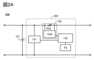
- FIGS. 2A and 2B are block diagrams showing specific configuration examples of current measurement circuit 152 in charger 201 included in power storage system 200 shown in FIGS. 1A and 1B.
- current measurement circuit 152 includes a resistor 152a and a circuit 152b.
- the resistor 152a has a function as a shunt resistor.
- the circuit 152b has the function of measuring the voltage across the resistor 152a.
- the current measurement circuit 152 is not limited to a resistance detection type configuration using a shunt resistor (resistance 152a) as shown in FIGS. 2A and 2B.
- the current measurement circuit 152 may have a magnetic field detection type configuration using, for example, a coil, a Hall element, a magnetoresistive element, a magnetoresistive element, a flux gate, or the like.
- FIGS. 3A and 3B are block diagrams showing other examples of power storage system 200.
- Power storage system 200 shown in FIGS. 3A and 3B includes a DC-DC converter 157, a circuit 158, and a diode 159 in addition to the configuration shown in FIGS. 2A and 2B.
- power storage system 200 may include a DC-DC converter 157.
- DC-DC converter 157 includes a voltage conversion circuit (not shown) and a control circuit (not shown).
- the DC-DC converter 157 has a function of converting the voltage of the secondary battery 121 and outputting it.
- power storage system 200 may include a circuit 158.
- the circuit 158 has a function as an AC adapter. That is, the circuit 158 has a function of converting AC power into DC power, for example. Further, the circuit 158 has a function of converting voltage, for example. Further, the circuit 158 has a function of providing the secondary battery 121 with electric power converted to direct current. Note that the circuit 158 may have a function of controlling the current value and voltage value to be applied when power is applied to the secondary battery 121. Further, the circuit 158 may have a function of controlling the current value and voltage value provided to the secondary battery 121 based on the signal provided from the control circuit 153.
- a diode 159 may be provided between the circuit 158 and the charger 201.
- Diode 159 has a function of suppressing reverse current flowing from charger 201 to circuit 158.
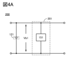
- FIG. 4A and 4B are block diagrams illustrating measurement of the voltage of secondary battery 121 by voltage measurement circuit 151 in power storage system 200.
- the voltage measurement circuit 151 measures the voltage Vb1 between the positive and negative electrodes of the secondary battery 121, and as shown in FIG. 4B, it divides the voltage Vb1 with resistance. There are two ways to measure the applied voltage.
- voltage Vb1 is resistively divided into voltage Vb2 and voltage Vb3 by resistor 122 and resistor 123.
- the voltage measurement circuit 151 measures the resistance-divided voltage Vb3.
- the voltage measurement circuit 151 or the control circuit 153 uses a resistor.
- the voltage Vb1 between the positive electrode and the negative electrode of the secondary battery 121 may be estimated from the divided voltage Vb3.
- the charger 201 has a function as a coulomb counter.
- the charger 201 uses the current measurement circuit 152 and the control circuit 153 to calculate the integrated quantity of electricity of the secondary battery 121, thereby determining the charging capacity (charging quantity of electricity) and discharging capacity of the secondary battery 121. It has a calculation function.
- the charger 201 may have a function of analyzing the charging depth using the calculated charging capacity (charging amount of electricity) and discharging capacity.
- the crystal structure of the positive electrode active material included in the secondary battery changes. If this change in crystal structure is irreversible, repeated charging may reduce the fully chargeable capacity of the secondary battery.
- the depth of charge of the secondary battery should be deepened, and the change in the crystal structure should be within a roughly reversible range. It is necessary to maintain the depth of charge of the battery.
- the charging depth of the secondary battery can be maintained so that the change in the crystal structure is approximately within a reversible range.
- the state of secondary batteries changes when they are repeatedly charged and discharged, so even when charging is performed with the same voltage as the upper limit, the depth of charge of the secondary battery increases as the number of charge/discharge cycles increases. It becomes difficult to make them the same. Therefore, in order to maintain the charging depth of the secondary battery so that the change in crystal structure is approximately within a reversible range, a means for monitoring the charging process is required.
- the charger of one embodiment of the present invention it is possible to monitor the charging process and maintain the depth of charge of the secondary battery so that the depth of charge is deep and the change in crystal structure is within a generally reversible range. can. Further, it is preferable to apply the positive electrode active material of one embodiment of the present invention to a secondary battery.
- the charger of one embodiment of the present invention can suppress collapse of the crystal structure of a positive electrode active material included in the secondary battery by controlling the charging conditions of the secondary battery. More specifically, for example, the charger of one embodiment of the present invention can increase the charging voltage of the secondary battery to the maximum within a range where collapse of the crystal structure can be suppressed, and can increase the reliability of the secondary battery. , high energy density can be achieved by efficiently utilizing secondary batteries to their limits.
- the charger of one embodiment of the present invention can suppress collapse of the crystal structure of the positive electrode active material having a layered crystal structure.
- a positive electrode active material having a layered crystal structure for example, metals serving as carrier ions are arranged in layers.
- metals serving as carrier ions are arranged in layers.
- lithium cobalt oxide lithium exists in a layered form between two CoO layers.
- when carrier ions are detached during charging distortion of the crystal, a change in the crystal structure due to the detachment of carrier ions, etc. may occur.
- lithium cobalt oxide when lithium ions are desorbed during charging, changes such as displacement of the two CoO layers and shortening of the interlayer distance between the two CoO layers may occur.
- a charging voltage may cause constituent elements of the positive electrode active material to be eluted into the electrolytic solution, leading to collapse of the crystal structure of the positive electrode active material. Furthermore, charging at a high voltage may cause decomposition reactions of elements constituting the electrolyte.
- a charger according to one embodiment of the present invention uses a simple method to detect changes in crystal structure, increases charging voltage to the maximum within a range that can ensure high reliability, and efficiently utilizes a secondary battery to the limit. be able to.
- the upper limit voltage for charging can be determined based on a waveform obtained during charging.
- the waveform can have various shapes, such as a curved line, a straight line, a combination of a curved line and a straight line, and the like.
- the waveform is not limited to a periodic wave. Examples of waveforms acquired during charging include a dQ/dV-V curve or a ⁇ V-t curve created from data on voltage, time, and current during charging.
- the charging voltage during repeated charging and discharging is preferably increased to the maximum, and even at the increased charging voltage, the crystal structure of the positive electrode active material
- the change in is substantially reversible.
- substantially reversible means that even if it is reversible or irreversible, deterioration due to repeated crystal structure changes is extremely small.
- the positive electrode active material of one embodiment of the present invention changes from the O3 type crystal structure to the O3' type crystal structure described below when the depth of charge of the secondary battery is approximately 80% or around 80%. Furthermore, when this change occurs, extreme values are observed in the dQ/dV curve and the like.
- a charger according to one embodiment of the present invention has a function of detecting this extreme value and controlling charging.
- the extreme value is near the upper limit voltage for charging.
- the extreme value caused by a change in the crystal structure is lower than the upper limit voltage for charging, and that the difference between the voltage at which the extreme value is detected and the upper limit voltage for charging is 0.15 V or less.
- the crystal structure of the positive electrode active material is approximately reversible during charging and discharging even if charging is performed for a predetermined time beyond the voltage at which the extreme value is detected. It is preferable to be able to change the Since the secondary battery to which the charger of one embodiment of the present invention is applied has such characteristics, the charger of one embodiment of the present invention can easily increase the efficiency of the secondary battery to the limit using the above extreme value.
- the upper limit voltage for charging can be controlled for better utilization.
- An extreme value caused by a change in the crystal structure is detected, for example, in a voltage time change curve of a secondary battery. Alternatively, it is detected in the time differential curve (dV/dt curve) of the voltage of the secondary battery.
- extreme values caused by changes in the crystal structure are detected, for example, in the voltage differential curve (dQ/dV curve) of the amount of electricity of the secondary battery.
- CCCV constant current, constant voltage
- constant current charging is performed, and after reaching the upper limit voltage of charging in constant current charging, constant voltage charging is performed.
- CCCV charging for example, by performing constant voltage charging at the upper limit voltage of constant current charging, charging can be carried out over time at the upper limit voltage, and the charging capacity (charging amount of electricity) is reduced due to deterioration of the secondary battery. It is less susceptible to changes in impedance, etc., and a charging capacity (charging amount of electricity) with small variations can be obtained.
- the charging capacity (charging amount of electricity) can be increased.
- charging at a high voltage may cause collapse of the crystal structure of the positive electrode active material, and may cause decomposition reactions of elements constituting the electrolyte. Therefore, constant voltage charging at the upper limit voltage may increase deterioration of the secondary battery.
- constant current charging because it can reduce the charging time at the upper limit voltage and extend the life of the secondary battery.
- the environmental temperature of the secondary battery exceeds 40° C.
- the secondary battery may significantly deteriorate during constant voltage charging at the upper limit voltage. Therefore, when the environmental temperature of the secondary battery is high, it is more preferable to perform constant current charging. Further, when the environmental temperature of the secondary battery is high, it is preferable not to use constant voltage charging at a high voltage or to shorten the time for constant voltage charging at a high voltage as much as possible.
- a positive electrode active material represented by the chemical formula AM y O Z (y > 0, z > 0), more specifically, for example, a positive electrode active material represented by the chemical formula AMO 2 .
- the positive electrode active material represented by the chemical formula AM y O Z (y>0, z>0), as well as element A and metal M will be described later.
- the positive electrode active material is expressed by the chemical formula AMO2
- the composition of A:M:O is not limited to 1:1:2.
- lithium cobalt oxide may be expressed as LiCoO 2 .
- lithium nickelate may be expressed as LiNiO 2 .
- a secondary battery is charged at a temperature of 35° C. or higher and 55° C. or lower so that the charging depth is 85% or less, or 80% or less, or 77% or less.
- the degree of charging can be expressed by using x in the compositional formula, for example, x in Li x CoO 2 , to indicate how much lithium that can be intercalated and deintercalated remains in the positive electrode active material.
- x (theoretical capacity ⁇ charging capacity (charging amount of electricity))/theoretical capacity.
- x in Li x CoO 2 is small, for example, 0.1 ⁇ x ⁇ 0.24.
- charging may be performed such that x is 0.2 or less, or 0.24 or less, or 0.3 or less.
- the upper limit voltage for charging is preferably 4.8 V or less, more preferably 4.8 V or less, with the positive electrode potential based on the lithium potential (Li/Li + ) at 35° C. or higher and 55° C. or lower. Charging is performed so that the voltage is .75V or less, more preferably 4.7V or less, even more preferably 4.65V or less.
- the charging rate (also referred to as capacity rate) is preferably 0.35C or higher, more preferably 0.45C or higher, and even more preferably 0.
- Charging is performed to a temperature of .7C or higher, more preferably 0.9C or higher.
- C here is a unit of rate.
- charging is performed to achieve the charging rate. conduct.
- the charging rate 1C is, for example, about 0.7 times the amount of electricity for charging and reacting the entire amount of element A (in the case of lithium cobalt oxide, element A is lithium) possessed by the positive electrode active material. Let be the current density for charging in 1 hour.
- the depth of charge is, for example, preferably 50% or more, more preferably 60% or more, even more preferably 70% or more, and even more preferably 73% or more. Further, the depth of charge may be higher than 75%.
- the method for calculating the depth of charge in a secondary battery is not limited to the example shown above.
- the charging depth corresponding to the rated capacity of the secondary battery may be set to 100%.
- the standardization of charging capacity (charging amount of electricity) used for charging depth is not limited to the example shown above. Standards are based on the volume of the secondary battery, the internal volume of the secondary battery, the volume of a portion of the secondary battery, the weight of the secondary battery, the weight of the contents of the secondary battery, the weight of a portion of the secondary battery, etc. may be converted into
- an extreme value caused by a change in the crystal structure of the positive electrode active material can be detected in a dQ/dV curve or the like, and constant current charging can be performed. Further, constant current charging using detection of the extreme value is simple and has good controllability. Therefore, by using the charger of one embodiment of the present invention, it is possible to realize a secondary battery with small variations in charging capacity (charging amount of electricity) and with suppressed deterioration due to high voltage charging.
- step S100 processing is started.
- step S101 constant current charging of the secondary battery is started at time t1. Note that the constant current charging is performed continuously until charging is stopped in step S107.
- step S102 the voltage measurement circuit 151 starts measuring the voltage of the secondary battery. Further, the current measurement circuit 152 starts measuring the current of the secondary battery. Voltage measurement circuit 151 provides the measured voltage value to control circuit 153. Current measurement circuit 152 provides the measured current value to control circuit 153.
- step S103 the control circuit 153 accumulates the voltage value measured by the voltage measurement circuit 151 and the current value measured by the current measurement circuit 152 from step S102 onwards, as set data with time.
- a memory circuit or the like included in the control circuit 153 can be used to accumulate data.
- the time from the start of charging may be used as the time associated with the voltage value and the current value.
- step S104 the control circuit 153 calculates a voltage differential curve (dQ/dV curve) of the amount of electricity of the secondary battery using the set data of the voltage value, current value, and time that are accumulated from time to time.
- step S103 may calculate a voltage differential curve of the amount of electricity of the secondary battery after accumulating data sets of a certain predetermined time, voltage value, current value, and time. For example, set data may be accumulated for a period sufficient to detect extreme values.
- step S105 the control circuit 153 analyzes a curve (hereinafter referred to as a dQ/dV-V curve) in which the horizontal axis is the voltage V and the vertical axis is the voltage differential dQ/dV of the quantity of electricity Q, and the extreme value ( (also referred to as a peak) is detected. If an extreme value, for example a local maximum (also referred to as an upwardly convex peak) is detected in the dQ/dV-V curve, the process advances to step S106. If not detected, the process returns to step S103. Note that a plurality of extreme values may be detected in the dQ/dV-V curve. In such a case, the highest extreme value among the plurality of extreme values is detected. Alternatively, among the plurality of extreme values, the top r extreme values (r is an integer of 2 or more) may be detected, and one of the r extreme values may be selected.
- a dQ/dV-V curve a curve in which the horizontal axis
- the upper extreme value refers to the higher value among the ranks determined based on predetermined conditions. For example, it may be arranged in descending order of the height of the extreme value.
- control circuit 153 continues to accumulate the set data of voltage value, current value, and time while repeating the steps from step S103 to step S105. That is, when repeating the steps from step S103 to step S105 n times, the dQ/dV-V curve can be calculated using all the data n times. Alternatively, among the n times, only the latest one or only the latest several times may be used.
- step S106 the control circuit 153 determines whether the voltage of the secondary battery is equal to or higher than a predetermined voltage. If the voltage V of the secondary battery is equal to or higher than the voltage V2, the process advances to step S107. If the voltage V is less than the voltage V2, the process returns to step S103.
- the voltage V2 is, for example, 4.25V or more, or 4.25 or more and less than 4.8V.
- the magnitude of the voltage V and the voltage V2 in step S106 may be determined based on the depth of charge of the secondary battery. For example, if the depth of charge of the secondary battery is S1% or more, the process may proceed to step S107, and if it is less than S1%, the process may return to step S103.
- S1 is 60[%] or more, or 60[%] or more and 95[%] or less.
- the control circuit 153 can continuously accumulate set data of voltage value, current value, and time from the first step S103 of the plurality of repeated steps S103 until proceeding to step S107.
- step S107 a time tp at which the dQ/dV-V curve takes an extreme value is detected by analysis, and charging is stopped at time t2, which is a predetermined time elapsed from time tp.
- the predetermined time is, for example, the time required for the control circuit 153 to stop charging.
- a region having a desired voltage width centered around the voltage that takes the extreme value is determined as time t2, and the time corresponding to the voltage at the upper end of the region is determined as time t2. You can. Note that if no extreme value is detected in step S107, charging may be stopped when a predetermined charging voltage is reached.
- step S107 Although detection of an extreme value is mentioned here as a condition for stopping charging in step S107, for example, an inflection point may be detected and charging stop may be controlled based on the elapsed time from the detected inflection point. Good too.
- the curve to be analyzed may be smoothed.
- a moving average may be used as the smoothing method.
- the inflection point detected at time tp is, for example, an inflection point resulting from a change in the crystal structure of the positive electrode active material included in the positive electrode of the secondary battery.
- the positive electrode active material of one embodiment of the present invention is used as the positive electrode active material and charging of the secondary battery is stopped at a time near time tp, the crystal structure of the positive electrode active material will not collapse due to repeated charging and discharging. can be suppressed.
- the crystal structure of the positive electrode active material changes from an O3 type crystal structure to an O3' type crystal structure.
- An inflection point corresponding to can be used.
- the positive electrode active material is, for example, lithium cobalt oxide.
- the charging voltage or charging depth at time t2 is preferably lower than the charging voltage at which the crystal structure of the positive electrode active material changes to the H1-3 type crystal structure, or shallower than the charging depth. Details of the O3 type crystal structure, O3' type crystal structure, and H1-3 type crystal structure will be described later. Note that this change from the O3 type crystal structure to the O3' type crystal structure may be expressed as a phase change.
- the crystal structure at time t2 can be controlled to be an O3' type crystal structure. Thereby, collapse of the crystal structure of the positive electrode active material during repeated charging and discharging of the secondary battery can be suppressed.
- the crystal structure determined is expressed by the space group R-3m. Further, it is more preferable that the determined crystal structure is expressed by the space group R-3m and that an O3' type crystal structure is suggested.
- the positive electrode when a positive electrode obtained by disassembling a secondary battery charged with the power storage system of one embodiment of the present invention in a charging state corresponding to time t2 is evaluated using an XRD pattern, the positive electrode corresponds to space group R-3m. A spectrum is observed. Regarding the measurement conditions, measurement method, etc., the description below can be referred to.
- the determined crystal structure is expressed by the space group R-3m.
- the crystal structure determined is expressed by the space group R-3m, so that the charge/discharge cycle is A secondary battery with less decrease in discharge capacity can be obtained.
- step S101 to step S107 are repeated s times.
- s is an integer of 2 or more.
- the time tp and time t2 determined based on the extreme values detected in steps S102 to S106 may be used in the next charging cycle.
- the time tp and time t2 obtained in the (s-1)th charging may be used as the conditions for stopping charging in step S107 of the sth charging.
- step S199 the process ends.
- the current value of constant current charging is set as a constant current value, for example, from when charging is started in step S101 until charging is stopped in step S107.
- the current value in constant current charging may be changed in stages after charging is started in step S101 until charging is stopped in step S107.
- steps S103 to S105 are repeated n times, the current value may be changed after a certain number of times.
- the charger of one embodiment of the present invention analyzes the charging characteristics of the secondary battery in steps S103 to S106, and changes the charging conditions of the secondary battery in step S107 according to the analyzed results. can. Specifically, for example, charging of the secondary battery can be stopped.
- the charging characteristics analyzed in steps S103 to S106 change depending on the environmental temperature during charging and discharging of the secondary battery, deterioration of the secondary battery due to charging and discharging cycles, and the like.
- the charger of one embodiment of the present invention suppresses deterioration of the secondary battery by changing the charging conditions of the secondary battery, such as the charging voltage of the secondary battery, in accordance with such changes in charging characteristics. be able to.
- the charger of one embodiment of the present invention can perform charging to the maximum within a range where deterioration of the secondary battery is suppressed.
- step S107 after time t2, constant voltage charging may be performed at a voltage lower than the upper limit charging voltage of constant current charging at time t2.
- Example 2 of charging method> An example of a charging method using the charger of one embodiment of the present invention will be described with reference to the flow diagram shown in FIG. Note that in the charging method shown in FIG. 6, the calculations performed by the control circuit 153 are simpler than those in the charging method shown in FIG. 5, and may be performed on a smaller circuit scale.
- dQ/dV can be expressed as in the following formula.
- dQ/dt is constant, so dQ/dV is proportional to dt/dV. Therefore, by evaluating the dt/dV characteristics during constant current charging, information similar to the dQ/dV characteristics can be obtained.
- dt/dV characteristics are evaluated in a region where constant current charging is performed.
- dt/dV characteristic it is not necessary to acquire the current value of the secondary battery every time, and it may be possible to acquire the dt/dV characteristic more easily than dQ/dV.
- calculations are simple and the circuit scale can be reduced in some cases.
- the scale of the storage circuit can be reduced in some cases.
- dQ/dV in constant current charging may change more slowly than dQ/dV in constant voltage charging.
- step S000 the process starts.
- step S001 constant current charging of the secondary battery is started at time t3. Note that the constant current charging is performed continuously until charging is stopped in step S007.
- step S002 the voltage measurement circuit 151 starts measuring the voltage of the secondary battery.
- Voltage measurement circuit 151 provides the measured voltage value to control circuit 153.
- step S003 the control circuit 153 accumulates the voltage values measured by the voltage measurement circuit 151 from step S002 onward as set data with the time.
- a memory circuit or the like included in the control circuit 153 can be used to accumulate data.
- the time from the start of charging may be used as the time associated with the voltage value.
- the obtained voltage value is converted from an analog value to a digital value in the control circuit 153.
- the control circuit 153 may use the obtained analog value for calculation without converting it into a digital value.
- an MCU is used as the control circuit 153 and a voltage value is converted using an analog-to-digital conversion circuit installed in the MCU.
- an MCU equipped with an analog-to-digital conversion circuit having 12-bit voltage resolution is used.
- the predetermined value may be, for example, the minimum value of the voltage resolution of the analog-to-digital conversion circuit, or may be a higher value.
- step S004 the control circuit 153 calculates the temporal change in the voltage of the secondary battery using the set data of the voltage value and time that are accumulated from time to time.
- the time change in voltage can be expressed as voltage [V(t)-V(t- ⁇ t1)] using voltage V(t) at time t and voltage V(t- ⁇ t1) at time (t- ⁇ t1). can be expressed.
- a curve of voltage change over time is sometimes called a ⁇ V-t curve.
- step S003 may calculate the time change after accumulating the set data of voltage value and time for a certain predetermined time. For example, set data may be accumulated for a period sufficient to detect extreme values.
- step S005 the control circuit 153 analyzes the time change curve (for example, ⁇ V-t curve) of the voltage of the secondary battery, and determines whether an extreme value is detected. If an extreme value, for example a minimum (also referred to as a downwardly convex peak) is detected in the time change curve, the process advances to step S006. If not detected, the process returns to step S003.
- a plurality of extreme values may be detected. In such a case, the highest extreme value among the plurality of extreme values is detected. Alternatively, among the plurality of extreme values, the top r extreme values (r is an integer of 2 or more) may be detected, and one of the r extreme values may be selected.
- control circuit 153 continuously accumulates the set data of voltage value and time while repeating the steps from step S003 to step S005. That is, when repeating the steps from step S003 to step S005 n times, the time change curve can be calculated using all the data n times. Alternatively, among the n times, only the latest one or only the latest several times may be used. Here, n is an integer of 1 or more.
- step S006 the control circuit 153 determines whether the voltage of the secondary battery is equal to or higher than a predetermined voltage. If the voltage V of the secondary battery is equal to or higher than the voltage V1, the process advances to step S007. If the voltage V is less than the voltage V1, the process returns to step S003.
- the voltage V1 is, for example, 4.25V or more, or 4.25V or more and less than 4.8V.
- the voltage measurement circuit 151 measures the voltage obtained by dividing the voltage between the positive electrode and the negative electrode of the secondary battery by resistance
- the voltage measured from the voltage obtained by dividing the voltage by resistance is used as the voltage V1.
- an estimated value of the voltage between the positive and negative electrodes of the next battery is used.
- the magnitude of the voltage V and the voltage V1 in step S006 may be determined based on the depth of charge of the secondary battery. For example, if the depth of charge of the secondary battery is S1% or more, the process may proceed to step S007, and if it is less than S1%, the process may return to step S003.
- S1 is 60[%] or more, or 60[%] or more and 95[%] or less.
- the control circuit 153 can continuously accumulate the set data of voltage value and time from the first step S003 of the plurality of repeated steps S003 until proceeding to step S007.
- step S007 a time tq at which the ⁇ V-t curve takes an extreme value is detected by analysis, and charging is stopped at time t4, which is a time when a predetermined time has elapsed from time tq.
- time t4 for example, a region having a desired width of time centered on the time at which the extreme value is obtained in the ⁇ V-t curve may be determined, and the time at the upper end of the region may be determined as time t4.
- the predetermined time is, for example, the time required for the control circuit 153 to stop charging. Note that if no extreme value is detected in step S007, charging may be stopped when a predetermined charging voltage is reached.
- step S007 detection of an extreme value is mentioned here as a condition for stopping charging in step S007, for example, an inflection point may be detected and charging stop may be controlled based on the elapsed time from the detected inflection point. Good too.
- time tq and time t4 determined based on the extreme values detected in steps S002 to S006 may be used in the next charging cycle.
- time tq and time t4 obtained in the (w-1)th charging may be used as conditions for stopping charging in step S007 of the w-th charging.
- step S099 the process ends.
- the current value of constant current charging is set as a constant current value, for example, from when charging is started in step S001 until charging is stopped in step S007.
- the current value in constant current charging may be changed in stages after charging is started in step S001 until charging is stopped in step S007.
- steps S003 to S005 are repeated n times, the current value may be changed after a certain number of times.
- step S200 the process starts.
- step S201 constant current charging of the secondary battery is started. Note that the constant current charging is performed continuously until charging is stopped in step S206.
- step S202 the voltage measurement circuit 151 starts measuring the voltage of the secondary battery.
- the measured voltage V is provided from the voltage measurement circuit 151 to the control circuit 153.
- step S203 the control circuit 153 compares the measured voltage V and a predetermined voltage V3. If the voltage V is equal to or higher than the voltage V3, the process advances to step S204, and if the voltage V is lower than the voltage V3, the process returns to step S202.
- step S204 the control circuit 153 evaluates dQ/dV.
- the value of dt/dV is measured.
- the value of dt/dV can be accumulated at any time during the charging process. Using the accumulated data set of voltage V and time t, a moving average [dt/dV] mean of dt/dV and a maximum value [dt/dV] max are calculated.
- the time required for the voltage to change by a predetermined value may be calculated as the value equivalent to dt/dV.
- the predetermined value may be, for example, 0.5 mV or more and 10 mV or less.
- step S205 the moving average [dt/dV] mean is compared with the value obtained by multiplying the maximum value [dt/dV] max by a constant Rt. If the moving average [dt/dV]mean is smaller than the value obtained by multiplying the maximum value [dt/dV]max by the constant Rt, the process advances to step S206. If the moving average [dt/dV]mean is greater than or equal to the value obtained by multiplying the maximum value [dt/dV]max by the constant Rt, the process returns to step S204.
- the time when the moving average [dt/dV] mean becomes smaller than the value obtained by multiplying the maximum value [dt/dV] max by the constant Rt is, for example, on the dt/dV curve, from the maximum value near voltage V3, This corresponds to the time when the value decreases to (Rt ⁇ 100) [%] of the maximum value.
- step S206 charging of the secondary battery is stopped.
- step S299 the process ends.
- FIG. 7 shows an example of constant current charging, but when the charging current is not constant, for example, the moving average of dt/dV [dt/dV] mean and the maximum value of voltage [dt /dV]max multiplied by a constant Rt, instead of comparing the average value of the quantity of electricity Q at the measurement time and times in its vicinity, and the value obtained by multiplying the maximum value of the quantity of electricity Q by a constant. All you have to do is compare.
- Example 1 of voltage measurement circuit As an example of the voltage measurement circuit 151 included in the charger 201, a voltage measurement circuit 151A will be described.
- FIG. 8 is a block diagram illustrating a configuration example of the voltage measurement circuit 151A.
- the voltage measurement circuit 151A includes a sample and hold circuit (S/H) 162, an S/H 174, a digital-to-analog conversion circuit (DAC) 172, a comparator 171, a control section 173, Equipped with
- the control unit 173 includes a signal processing circuit 173a, a timing circuit 173b, and a register 173c.
- FIG. 8 illustrates a secondary battery 121 and a control circuit 153 that are electrically connected to the voltage measurement circuit 151A in the power storage system 200.
- the voltage is a voltage based on the potential of the negative electrode of the secondary battery 121.
- the voltage measurement circuit 151A has a function as a successive approximation type analog-to-digital conversion circuit (ADC). Further, the voltage measurement circuit 151A has a function of calculating the time required for the input voltage to change by a predetermined voltage value (for example, 1 mV) (also referred to as a time difference or a time difference), and outputting the time. Therefore, the voltage measurement circuit 151A may be called, for example, a difference device or a time measurement circuit.
- ADC successive approximation type analog-to-digital conversion circuit
- the S/H 162 has a function of acquiring (sampling) and holding the voltage Vbp of the positive electrode of the secondary battery 121 in accordance with the signal SMP1. It also has a function of supplying the held voltage Vin to the inverting input terminal of the comparator 171.
- the S/H 174 has a function of acquiring and holding the voltage output from the DAC 172 in accordance with the signal SMP2. It also has a function of supplying the held voltage Vref to the non-inverting input terminal of the comparator 171.
- the DAC 172 has a function of outputting an analog voltage based on digital voltage data stored in the register 173c.
- the comparator 171 compares the magnitude of the voltage Vin and the voltage Vref, and based on the comparison result, a voltage (H level) corresponding to digital data "1” or a voltage (H level) corresponding to digital data "0" It has the function of outputting (L level).
- the signal processing circuit 173a has a function of performing various processes depending on, for example, the output of the comparator 171 and the signal from the timing circuit 173b. As various types of processing, the signal processing circuit 173a has a function of updating voltage data stored in the register 173c, for example. Further, the signal processing circuit 173a has a function of outputting, for example, voltage data (data OUTV) stored in the register 173c and time data (data OUTt) from the timing circuit 173b to the control circuit 153. Further, the signal processing circuit 173a has a function of outputting a signal SMP2 for controlling the operation of the S/H 174, for example. Further, the signal processing circuit 173a has a function of outputting a signal WKUP and a signal SLEP for transmitting the operating state of the voltage measurement circuit 151A to the control circuit 153, for example.
- the timing circuit 173b has a function of performing various processes according to, for example, a signal from the signal processing circuit 173a and a signal STUP given from the control circuit 153. As various processes, the timing circuit 173b has a function of outputting a signal SMP1 for controlling the operation of the S/H 162, for example. Further, the timing circuit 173b has a function of measuring time, for example. In the timing circuit 173b, for example, a counter (not shown), an oscillator (not shown), etc. can be used to measure the time. Further, for example, the count value of the counter can be used as time data.
- the register 173c has a function of storing voltage data.
- Each circuit (for example, S/H 162, S/H 174, DAC 172, comparator 171, signal processing circuit 173a, timing circuit 173b, register 173c, etc.) constituting the voltage measurement circuit 151A is a transistor containing silicon in a channel formation region ( (Si transistor) or a circuit including a Si transistor.
- the voltage measurement circuit 151A can be said to be a semiconductor device.
- part or all of each of the circuits may include a transistor including an oxide semiconductor in a channel formation region (OS transistor), or a circuit including the OS transistor.
- the OS transistor Since the band gap of the oxide semiconductor in which the channel is formed is 2 eV or more, the OS transistor has a characteristic that off-state current (current flowing between the source and drain when the transistor is off) is extremely low.
- the off-state current value of the OS transistor per 1 ⁇ m channel width at room temperature is 1aA (1 ⁇ 10 ⁇ 18 A) or less, 1zA (1 ⁇ 10 ⁇ 21 A) or less, or 1yA (1 ⁇ 10 ⁇ 24 A) or less It can be done.
- the off-state current value per 1 ⁇ m of channel width at room temperature is 1 fA (1 ⁇ 10 ⁇ 15 A) or more and 1 pA (1 ⁇ 10 ⁇ 12 A) or less. Therefore, it can be said that the off-state current of an OS transistor is about 10 orders of magnitude lower than that of a Si transistor.
- the off-state current of the OS transistor hardly increases even in a high temperature environment. Specifically, the off-state current hardly increases even under an environmental temperature of room temperature or higher and 200° C. or lower. Furthermore, the on-state current of the OS transistor does not easily decrease even in a high-temperature environment.
- the on-state current of a Si transistor decreases in a high-temperature environment. That is, an OS transistor has a higher on-state current than a Si transistor in a high-temperature environment. Furthermore, the OS transistor can perform a good switching operation even under an environmental temperature of 125° C. or higher and 150° C. or lower because it has a large ratio of on-current to off-current. Therefore, a semiconductor device including an OS transistor operates stably even in a high-temperature environment and has high reliability.
- the semiconductor layer of the OS transistor contains at least one of indium and zinc.
- the semiconductor layer of the OS transistor is made of, for example, indium, M (M is gallium, aluminum, yttrium, tin, silicon, boron, copper, vanadium, beryllium, titanium, iron, nickel, germanium, zirconium, molybdenum, lanthanum). , cerium, neodymium, hafnium, tantalum, tungsten, magnesium, and cobalt) and zinc.
- M is preferably one or more selected from gallium, aluminum, yttrium, and tin.
- an oxide containing indium (In), gallium (Ga), and zinc (Zn) also referred to as "IGZO”
- an oxide containing indium (In), aluminum (Al), and zinc (Zn) also referred to as "IAZO”
- an oxide containing indium (In), aluminum (Al), gallium (Ga), and zinc (Zn) also referred to as "IAGZO”
- IAGZO oxide containing indium (In), aluminum (Al), gallium (Ga), and zinc (Zn)
- the atomic ratio of In in the In-M-Zn oxide is preferably equal to or higher than the atomic ratio of M.
- the atomic ratio of In in the In-M-Zn oxide may be smaller than the atomic ratio of M.
- the nearby composition includes a range of plus or minus 30% of the desired atomic ratio.
- the off-state current of the OS transistor is extremely low, so that charges accumulated in the capacitor can be retained for a long period of time. Therefore, the storage circuit can continue to store data for a long period of time by associating the level of potential depending on the amount of charge held in the capacitor with digital data of "1" or "0". Thereby, for example, a non-volatile memory can also be constructed.
- An OS transistor or a memory circuit using an OS transistor can be provided in part or all of each circuit constituting the voltage measurement circuit 151A.
- an OS transistor as a transistor constituting the S/H 174
- the voltage Vref held in the S/H 174 can be maintained for a long period of time even when the power supply to the DAC 172 is stopped.
- the voltage data stored in the register 173c can be continued to be stored for a long period of time even when the power supply to the register 173c is stopped. be able to.
- the voltage measurement circuit 151A can be placed in sleep mode until the input voltage changes by a predetermined voltage value, in other words, while the change in the input voltage is smaller than the predetermined voltage value.
- a predetermined voltage value in other words, while the change in the input voltage is smaller than the predetermined voltage value.
- the supply of power to the DAC 172 and the register 173c can be stopped.
- part of the operation of the signal processing circuit 173a may be stopped by, for example, power gating or clock gating.
- the signal processing circuit 173a can output the signal SLEP.
- the voltage measurement circuit 151A can maintain the voltage Vref held in the S/H 174 and continue to store the voltage data stored in the register 173c. Therefore, even in the sleep mode, the S/H 162 can acquire the voltage Vbp, and the comparator 171 can compare the voltage Vin and the voltage Vref.
- the voltage measurement circuit 151A can wake up from the sleep mode by changing the output of the comparator 171 when the input voltage changes by a predetermined voltage value in the sleep mode. By waking up, for example, the supply of power to the DAC 172 and the register 173c can be restarted. Further, the operation of the signal processing circuit 173a can be restarted. Furthermore, upon wake-up, the signal processing circuit 173a can output the signal WKUP.
- an OS transistor or a memory circuit using an OS transistor may be provided as part of the control circuit 153.
- the control circuit 153 when the signal SLEP is applied, a part of the operation is stopped by power gating or clock gating, and when the signal WKUP is applied, the operation is restarted. Good too.
- FIG. 9 is a flow diagram illustrating an example of the operation of the voltage measurement circuit 151A.
- step S300 a signal STUP is applied from the control circuit 153 to start processing. Note that it is assumed that the secondary battery 121 is being charged with a constant current.
- steps S301 to S303 the analog input voltage is converted to digital voltage data and stored in the register 173c.
- steps S301 to S303 "1" or "0" is determined by successively comparing bit by bit from the most significant bit to the least significant bit.
- step S301 the register 173c is initialized. That is, only the most significant bit of the register 173c is set to "1", and the rest are all set to "0". For example, if the register 173c is 16 bits, the data in the register 173c is "1000000000000000”. The data in the register 173c is converted into an analog voltage by the DAC 172, and the S/H 174 holds this voltage as the voltage Vref. Further, the S/H 162 acquires the voltage Vbp of the positive electrode of the secondary battery 121 and holds it as the voltage Vin. After completing step S301, the process advances to step S302.
- step S302 it is determined whether the voltage Vbp (the voltage Vin acquired and held by the S/H 162 in step S301) is greater than the voltage Vref. That is, if the voltage Vin is larger than the voltage Vref, the comparison bit is determined to be "1" in step S3021. Alternatively, if the voltage Vin is less than or equal to the voltage Vref, the comparison bit is determined to be "0" in step S3022. After completing step S3021 or step S3022, the process advances to step S303.
- step S303 it is determined whether the data in the register 173c has been determined down to the least significant bit. If the lowest bit has not been determined, the next lower bit of the register 173c is set to "1" and the process returns to step S302. Alternatively, if the least significant bit has been determined, the process advances to step S304. For example, if the register 173c has 16 bits, it is possible to determine up to the least significant bit by repeating steps S302 and S303 16 times.
- step S304 the voltage data of the register 173c and the time data (count value of the counter) of the timing circuit 173b are outputted, and the process shifts to sleep mode.
- a signal SLEP is output.
- the data in the register 173c is updated to a higher value by a predetermined data value (for example, a data value corresponding to 1 mV).
- the voltage output from the DAC 172 increases by a predetermined voltage value (for example, 1 mV), and the voltage is held in the S/H 174.
- the voltage Vref held in the S/H 174 is increased by a predetermined voltage value, and then the sleep mode is entered.
- steps S311 to S314 the time required for the input voltage to change by a predetermined voltage value is calculated, and the time is output.
- step S311 the voltage Vbp is acquired by the S/H 162 at regular intervals (for example, 100 ms) and held as the voltage Vin. Further, the comparator 171 compares the voltage Vin and the voltage Vref. After completing step S311, the process advances to step S312.
- step S312 voltage Vbp (voltage Vin acquired and held by S/H 162 in step S311) becomes higher than voltage Vref, so that the output of comparator 171 changes (for example, changes from H level to L level).
- a signal WKUP is output.
- voltage data from the register 173c and time data from the timing circuit 173b are output.
- step S313 the process advances to step S313.
- difference time data may be output by calculating the difference between the count value of the counter when outputting last time and the count value of the counter when outputting this time.
- the data on the time difference is data on the time required for the input voltage to change by a predetermined voltage value.
- step S313 it is determined whether the conditions for stopping charging are met.
- the conditions for stopping charging for example, the conditions described in the above-mentioned charging method example 1 to charging method example 3 can be used as appropriate. If the conditions for stopping charging are met, the process ends in step S399. Alternatively, if the conditions for stopping charging are not met, the process advances to step S314.
- step S399 in the power storage system 200, a signal is sent to the control circuit 153 to notify that the conditions for stopping charging are satisfied so that the constant current charging of the secondary battery 121 by the charger 201 is stopped. good.
- step S314 the data in the register 173c is updated to a higher value by a predetermined data value.
- the voltage output from the DAC 172 increases by a predetermined voltage value, and the voltage is held in the S/H 174. That is, the voltage Vref held in the S/H 174 is increased by a predetermined voltage value. After that, it outputs the signal SLEP and shifts to sleep mode again. After completing step S314, the process returns to step S311.
- the voltage measurement circuit 151A can calculate the time required for the voltage Vbp of the secondary battery 121 to change by a predetermined voltage value (for example, 1 mV), and can output the time. Further, the voltage measurement circuit 151A can be placed in sleep mode until the voltage Vbp changes by a predetermined voltage value, in other words, while the change in the voltage Vbp is smaller than the predetermined voltage value.
- the voltage measurement circuit 151A can stop supplying power to the DAC 172 and the register 173c, and also stop part of the operation of the signal processing circuit 173a. This allows the power consumption of the voltage measurement circuit 151A to be reduced.
- the time required for the voltage Vbp to increase by a predetermined voltage value can be calculated.
- the time required for the voltage Vbp to decrease by a predetermined voltage value may be calculated.
- the data in the register 173c may be updated to data that is lower by a predetermined data value.
- the voltage Vref held in the S/H 174 may be lowered by a predetermined voltage value.
- a charger that can be used in the power storage system of one embodiment of the present invention can reduce power consumption by including the voltage measurement circuit 151A.
- Example 2 of voltage measurement circuit> As another configuration example of the voltage measurement circuit 151 included in the charger 201, a voltage measurement circuit 151B will be described.
- the voltage measurement circuit 151B is a modification of the voltage measurement circuit 151A described above. Therefore, in order to reduce the repetition of explanation, mainly the differences between the voltage measurement circuit 151B and the voltage measurement circuit 151A will be explained. Note that the description of the voltage measurement circuit 151A mentioned above can be referred to as appropriate.
- FIG. 10 is a block diagram illustrating a configuration example of the voltage measurement circuit 151B.
- the voltage measurement circuit 151B includes an integration circuit 175 and a selection circuit 176 in addition to the configuration of the voltage measurement circuit 151A described above. Further, the voltage measurement circuit 151B differs from the voltage measurement circuit 151A in that it does not need to include the S/H 162. Further, the voltage measurement circuit 151B includes, in the control unit 173, an oscillator 173d in the timing circuit 173b, an AND circuit 173e, and a counter 173f, in addition to the configuration of the voltage measurement circuit 151A described above.
- the voltage measurement circuit 151B has a function as a double integration type analog-to-digital conversion circuit (ADC). Further, the voltage measurement circuit 151B has a function of calculating the time (also referred to as difference time or time difference) required for the input voltage to change by a predetermined voltage value (for example, 1 mV) and outputting the time. Therefore, the voltage measurement circuit 151B may be called, for example, a difference device or a time measurement circuit.
- ADC analog-to-digital conversion circuit
- the selection circuit 176 has a function of applying either the voltage Vin (voltage Vbp) or the voltage Vref to the input terminal of the integrating circuit 175 in accordance with the signal SEL.
- the integrating circuit 175 has a function of integrating the voltage (either voltage Vin or voltage Vref) applied to the input terminal and providing the integrated voltage Vin2 to the output terminal.
- Integrating circuit 175 includes an operational amplifier 175a, a resistor 175r, and a capacitor 175c.
- the inverting input terminal of the operational amplifier 175a is electrically connected to one terminal of a resistor 175r and one terminal of a capacitor 175c.
- a non-inverting input terminal of the operational amplifier 175a is electrically connected to the wiring to which the voltage Vref2 is applied.
- the output terminal of the operational amplifier 175a is electrically connected to the other terminal of the capacitor 175c and the output terminal of the integrating circuit 175.
- the other terminal of the resistor 175r is electrically connected to the input terminal of the integrating circuit 175. Note that in the integrating circuit 175, it is preferable to provide a switch (not shown) having a function of making conductive or non-conductive between one terminal and the other terminal of the capacitor 175c.
- the output terminal of the integrating circuit 175 is electrically connected to the inverting input terminal of the comparator 171. That is, the voltage Vin2 applied to the output terminal of the integrating circuit 175 is applied to the inverting input terminal of the comparator.
- the comparator 171 has a function of comparing the magnitude of the voltage Vin2 applied to the inverting input terminal and the voltage Vref2 applied to the non-inverting input terminal, and outputs an H level or an L level based on the comparison result. .
- the oscillator 173d has a function of outputting clock pulses.
- the AND circuit 173e has a function of calculating the logical product of the clock pulse given from the oscillator 173d and the signal given from the signal processing circuit 173a, and outputting a signal CCK.
- the counter 173f has a function of counting the number of clock pulses given as the signal CCK. Further, the counter 173f has a function of resetting the count value in response to the signal CRE. Further, the counter 173f has a function of outputting a count value (data OUTC).
- the signal processing circuit 173a has a function of outputting a signal SEL for controlling the operation of the selection circuit 176, for example. Further, the signal processing circuit 173a has a function of controlling, for example, whether or not the clock pulse output from the oscillator 173d is applied to the counter 173f using an AND circuit 173e. Further, the signal processing circuit 173a has a function of outputting a signal CRE for controlling the operation of the counter 173f, for example. Further, the signal processing circuit 173a has a function of outputting voltage data (data OUTV) based on the data OUTC output from the counter 173f to the control circuit 153, for example.
- data OUTV voltage data
- the register 173c may have a function of storing data OUTC output from the counter 173f.
- a storage circuit (not shown) may be provided in the register 173c to store the data OUTC.
- each circuit constituting the voltage measurement circuit 151B can be provided with an OS transistor or a memory circuit using an OS transistor, similarly to the voltage measurement circuit 151A described above.
- the voltage measurement circuit 151B enters the sleep mode until the input voltage changes by a predetermined voltage value, in other words, while the change in the input voltage is smaller than the predetermined voltage value. It can be done.
- the voltage measurement circuit 151B can perform analog-to-digital conversion (A/D conversion), which will be described later, even in sleep mode.
- FIG. 11 is a schematic diagram illustrating analog-to-digital conversion (A/D conversion) in the voltage measurement circuit 151B.
- FIG. 11 shows how the voltage Vin2 output from the integrating circuit 175 changes over time when performing A/D conversion.
- the case where the voltage Vin is increased is shown by a broken line (vc2) with respect to the solid line (vc1).
- a dotted line (vc3) indicates the case where the voltage Vref is higher than the solid line (vc1).
- the selection circuit 176 is controlled and the voltage Vin is input to the integration circuit 175. Then, the voltage Vin2 decreases with a slope of "-(voltage Vin-voltage Vref2)/(Cv ⁇ Rv)".
- the selection circuit 176 is controlled and the voltage Vref is input to the integration circuit 175. Then, the voltage Vin2 increases with a slope of "-(voltage Vref-voltage Vref2)/(Cv ⁇ Rv)". At this time, control is performed so that the clock pulse output from the oscillator 173d is applied to the counter 173f. Then, the counter 173f starts counting.
- the output of the comparator 171 changes (for example, changes from H level to L level). At this time, the count value of the counter 173f is output.
- the count value output from the counter 173f is the value counted during the period ttb (period ttb1, period ttb2, or period ttb3) from inputting the voltage Vref to the integrating circuit 175 until the voltage Vin2 reaches the voltage Vref2. , and has a positive correlation with the voltage Vin input to the integrating circuit 175.
- the count value of the counter 173f is a value based on the voltage Vin.
- FIG. 12 is a flow diagram illustrating an example of the operation of the voltage measurement circuit 151B.
- step S400 a signal STUP is applied from the control circuit 153 to start processing. Note that it is assumed that the secondary battery 121 is being charged with a constant current.
- voltage Vin2 voltage Vref2.
- a switch provided between one terminal and the other terminal of the capacitor 175c is controlled to be in a conductive state.
- step S401 analog input voltage is converted into digital voltage data.
- step S401 the above-mentioned A/D conversion is performed to obtain data OUTC based on the voltage Vbp (voltage Vin).
- Vbp voltage Vin
- a switch provided between one terminal and the other terminal of the capacitor 175c is controlled to be in a non-conducting state.
- the data OUTC obtained here is stored as a predetermined count value.
- the predetermined count value may be stored in a storage circuit provided in the register 173c for storing data OUTC.
- step S402 the voltage data based on the data OUTC and the time data of the timing circuit 173b are outputted, and a transition is made to sleep mode.
- a signal SLEP is output.
- the data in the register 173c is updated to a higher value by a predetermined data value (for example, a data value corresponding to 1 mV).
- the voltage output from the DAC 172 increases by a predetermined voltage value (for example, 1 mV), and the voltage is held in the S/H 174.
- the voltage Vref held in the S/H 174 is increased by a predetermined voltage value, and then the sleep mode is entered.
- steps S411 to S414 the time required for the input voltage to change by a predetermined voltage value is calculated, and the time is output.
- step S411 the above-mentioned A/D conversion is performed at fixed time intervals (for example, 100 ms) to obtain data OUTC based on the voltage Vbp. At this time, since the voltage Vref was increased by a predetermined voltage value in the previous step, the data OUTC becomes a value lower than the predetermined count value even if the voltage Vbp is the same value. After completing step S411, the process advances to step S412.
- step S412 the voltage Vbp increases by a predetermined voltage value, so that the data OUTC becomes a predetermined count value. This causes the computer to return (wake up) from sleep mode. At this time, a signal WKUP is output. After returning from the sleep mode, voltage data based on the data OUTC and time data of the timing circuit 173b are output. After completing step S412, the process advances to step S413.
- step S412 data on the difference in time between the previous output and the current output may be output as the time data, similar to the voltage measurement circuit 151A described above. That is, the data on the time difference is data on the time required for the input voltage to change by a predetermined voltage value.
- step S413 it is determined whether the conditions for stopping charging are met.
- the conditions for stopping charging for example, the conditions described in the above-mentioned charging method example 1 to charging method example 3 can be used as appropriate. If the conditions for stopping charging are met, the process ends in step S499. Alternatively, if the conditions for stopping charging are not met, the process advances to step S414.
- step S414 the data in the register 173c is updated to higher data by a predetermined data value.
- the voltage output from the DAC 172 increases by a predetermined voltage value, and the voltage is held in the S/H 174. That is, the voltage Vref held in the S/H 174 is increased by a predetermined voltage value. After that, it outputs the signal SLEP and shifts to sleep mode again. After completing step S414, the process returns to step S411.
- the voltage measurement circuit 151B can calculate the time required for the voltage Vbp of the secondary battery 121 to change by a predetermined voltage value (for example, 1 mV) and output the time. Further, the voltage measurement circuit 151B can be placed in sleep mode until the voltage Vbp changes by a predetermined voltage value, in other words, while the change in the voltage Vbp is smaller than the predetermined voltage value.
- the voltage measurement circuit 151B can stop supplying power to the DAC 172 and the register 173c, and also stop part of the operation of the signal processing circuit 173a. This allows the power consumption of the voltage measurement circuit 151B to be reduced.
- the time required for the voltage Vbp to increase by a predetermined voltage value can be calculated.
- the time required for the voltage Vbp to decrease by a predetermined voltage value may be calculated.
- the data in the register 173c may be updated to data that is lower by a predetermined data value.
- the voltage Vref held in the S/H 174 may be lowered by a predetermined voltage value.
- a charger that can be used in the power storage system of one embodiment of the present invention can reduce power consumption by including the voltage measurement circuit 151B.
- the charger according to one embodiment of the present invention preferably has a function of estimating the SOH (State of Health) of the secondary battery.
- SOH is an index representing the capacity that can be fully charged at a certain point in time, based on the capacity that can be fully charged in a new state.
- SOH is a numerical value expressed as a value smaller than 100 as the secondary battery deteriorates, with the fully chargeable capacity of the secondary battery in a new state being 100, and the unit is "%".
- the intensity of the extreme values may decrease. This decrease in strength may be due to a phase change corresponding to the extreme value becoming less likely to occur in the positive electrode active material, and may have a correlation with, for example, SOH.
- the charger according to one embodiment of the present invention preferably has a function of estimating the SOH by observing the intensity of the extreme value of the dQ/dV-V curve.
- the charger according to one embodiment of the present invention preferably has a function of estimating the dischargeable capacity of the secondary battery by observing the intensity of the extreme value of the dQ/dV-V curve.
- the charger 201 preferably controls charging using temperature.
- control circuit 153 changes the charging conditions according to the environmental temperature of the secondary battery measured by the temperature sensor TS.
- the memory circuit included in the control circuit 153 has, for example, a table in which the environmental temperature of the secondary battery and charging conditions are linked.
- the storage circuit included in the control circuit 153 stores charging characteristics associated with the environmental temperature of the secondary battery.
- the charging characteristic may be a past measured value of the secondary battery 121, a measured value of another secondary battery having similar characteristics, or a waveform obtained by calculation. Good too.
- extreme values (peaks) may be estimated using these measured values. For example, machine learning or the like can be used for the estimation.
- the control circuit 153 may use the charging characteristics of the secondary battery stored in the memory circuit to analyze extreme values in the differential curves of voltage and quantity of electricity.
- the charging characteristic for example, a capacity-voltage curve, a voltage-dQ/dV curve, a ⁇ V-t curve, an impedance characteristic, etc. can be used.
- the temperature sensor TS may be, for example, a temperature measuring resistor (for example, platinum, nickel, or copper), a thermistor (PTC (Positive Temperature Coefficient) thermistor, or NTC (Negative Temperature Coefficient) thermistor). , thermocouple, or An IC temperature sensor or the like may be used.
- a configuration using a semiconductor temperature sensor for example, a silicon diode temperature sensor, etc.
- a configuration using a bandgap circuit may be used as the temperature sensor TS.
- NTC thermistor has a characteristic that its resistance value gradually decreases as the temperature rises. Therefore, it can be used, for example, for detailed temperature detection or simple inrush current suppression. Further, a PTC thermistor (PTC element) has a characteristic that its resistance value increases rapidly when a certain temperature is exceeded. Therefore, it can be used for overheat detection, overcurrent protection, inrush current suppression, etc., for example.
- FIG. 1B shows that the charger 201 has, in addition to the configuration shown in FIG. An example including a detection circuit SD, a micro short detection circuit MSD, a transistor 140, and a transistor 150 is shown.
- the charger 201 shown in FIG. 1B has a function of suppressing overcharging, overdischarging, charging overcurrent, discharging overcurrent, short circuit, micro short circuit, etc., and can function as a protection circuit for a secondary battery.
- a micro short refers to a minute short circuit inside the secondary battery, and the short circuit current is not so great that the positive and negative electrodes of the secondary battery are shorted and cannot be charged, but the short circuit current is small at the minute short circuit. Refers to the phenomenon of flowing away. A large voltage change may occur even in a relatively short period of time and at a small location.
- a transistor called a power MOSFET can be used as the transistor 140 and the transistor 150.
- the control circuit 153 has a function of cutting off the current flowing to the secondary battery 121 by applying signals to the gates of the transistor 140 and the transistor 150, respectively.
- the detection circuit 185 monitors the voltage of the secondary battery, and when overcharging or overdischarging is detected, it can provide a signal indicating the detection to the control circuit 153.
- the control circuit can receive the signal, apply the signal to at least one of the gate of transistor 140 and the gate of transistor 150, and cut off the current flowing to secondary battery 121.
- the detection circuit 186 monitors the current of the secondary battery 121, and when detecting an overcurrent during charging or discharging, can provide a signal indicating the detection to the control circuit 153.
- the control circuit can receive the signal, apply the signal to at least one of the gate of transistor 140 and the gate of transistor 150, and cut off the current flowing to secondary battery 121.
- Overcharging detected by the detection circuit 185 corresponds to the extreme value of the charging voltage time change curve (for example, ⁇ V-t curve) or the extreme value of the voltage differential curve of charging electricity (dQ/dV curve). may be used for detection.
- overcharging detected by the detection circuit 185 may be detected by comparing it with a predetermined voltage value using a comparison circuit. Different values may be used as the predetermined voltage value depending on the environmental temperature of the secondary battery.
- the voltage value corresponding to the environmental temperature of the secondary battery is stored, for example, in a memory circuit included in the control circuit 153.
- the power storage system 200 shown in FIGS. 13A to 13C shows an example in which a charger 201 is connected to each of m secondary batteries 121 connected in series.
- FIG. 13A shows an example of the power storage system 200 where m is an integer of 4 or more, and among m secondary batteries 121, the first, second, third, and m-th secondary batteries 121 are Secondary battery 121(1), secondary battery 121(2), secondary battery 121(3), and secondary battery 121(m) are illustrated, and other secondary batteries are omitted.
- FIG. 13B shows an example of the power storage system 200 when m is 3
- FIG. 13C shows an example of the power storage system 200 when m is 2.
- the detection circuit 185 included in the charger 201 has a terminal 124 electrically connected to the positive electrode of the secondary battery 121(1), and a terminal 125 electrically connected to the negative electrode of the secondary battery 121(m). Overcharging may be detected at voltages between . Further, for example, the detection circuit 186 and the short detection circuit SD included in the charger 201 may detect overcharging or short circuit based on the current between the terminal 124 and the terminal 125.
- the power storage system 200 can independently control the m secondary batteries 121 using the chargers 201 connected to each one.
- a path connected in parallel to the secondary battery 121 for example, a transistor, a resistance element, or Allow the current to flow through a diode, etc. Therefore, it is preferable that the charger 201 has, as a current path, a switch that switches between the secondary battery 121 and the current path.
- the power storage system 200 has m secondary batteries 121 connected in series, the total voltage of the m secondary batteries (for example, in FIG. 13A, the positive electrode of the secondary battery 121(1) and the Charging may be controlled using the voltage across the negative electrode of the battery 121 (m). In such a case, a voltage value multiplied by m can be used as the voltage used to control charging.
- the secondary battery of one embodiment of the present invention preferably includes a positive electrode, a negative electrode, and an electrolyte.
- a positive electrode according to one embodiment of the present invention includes a positive electrode active material.
- a positive electrode active material that can be used in a secondary battery of one embodiment of the present invention and a method for manufacturing the same will be described with reference to FIGS. 14A to 23C.
- FIGS. 14A and 14B are cross-sectional views of a positive electrode active material 100 that can be used in a secondary battery according to one embodiment of the present invention.
- FIGS. 14C and 14D are enlarged views of the area around AB in FIG. 14A.
- FIGS. 14E and 14F are enlarged views of the area around CD in FIG. 14A.
- the positive electrode active material 100 has a surface layer portion 100a and a bulk 100b.
- the boundary between the surface layer portion 100a and the bulk 100b is indicated by a broken line.
- FIG. 14B a part of the grain boundary 101 is shown by a dashed line.
- the positive electrode active material 100 is a compound containing oxygen and a transition metal capable of intercalating and deintercalating lithium. Therefore, the interface between the region where the transition metal M (for example, Co, Ni, Mn, Fe, etc.) or oxygen, which is oxidized and reduced as lithium is intercalated and deintercalated, and the region where oxygen is not present is defined as the surface of the positive electrode active material.
- a surface caused by at least one of slips, cracks, and cracks can also be referred to as the surface of the positive electrode active material.
- the surface of the positive electrode active material in line analysis of EDX (Energy Dispersive The measurement point showing the measurement value closest to 50% of the value is taken as the measurement point.
- the intersection point is the tangent drawn to the intensity profile of the EDX-ray analysis of the transition metal or oxygen and the axis in the depth direction.
- the measured value closest to 50% of the average value of the detected amounts of the transition metal and oxygen in the bulk is different, the one located on the outer side can be adopted.
- the surface layer portion 100a of the positive electrode active material 100 refers to a region within 10 nm perpendicularly or substantially perpendicularly from the surface toward the inside. Or it refers to a region within 50 nm. Or a region within 5 nm.
- Surface layer portion is synonymous with near surface, near surface region, or shell. Note that "substantially perpendicular” is defined as 80° or more and 100° or less.
- a region deeper than the surface layer portion 100a of the positive electrode active material is referred to as a bulk 100b.
- Bulk 100b is synonymous with interior or core.
- the surface of the positive electrode active material 100 refers to the surface of the composite oxide including the surface layer portion 100a, the bulk 100b, the convex portions 103, and the like. Note that the positive electrode active material 100 does not contain carbonate, hydroxyl groups, etc. that were chemically adsorbed after the positive electrode active material 100 was produced. Further, it is assumed that the electrolyte, organic solvent, binder, conductive material, or compounds derived from these that adhere to the cathode active material 100 after the fabrication thereof are not included in the cathode active material 100. In addition, the surface of the positive electrode active material 100 in a cross-sectional STEM image, etc.
- the point should be the outermost area of the area to be checked.
- the surface in a cross-sectional STEM image or the like may be determined in conjunction with the results of analysis with higher spatial resolution, such as EELS (Electron Energy Loss Spectroscopy).
- the crystal grain boundaries 101 are, for example, areas where the positive electrode active materials 100 are stuck to each other, or areas where the crystal orientation changes inside the positive electrode active materials 100, that is, where the repetition of bright lines and dark lines in a STEM image etc. becomes discontinuous.
- crystal defects refer to defects that can be observed in cross-sectional TEM images, cross-sectional STEM images, etc., that is, structures where other atoms enter between lattices, cavities, etc.
- the grain boundary 101 can be said to be one of the planar defects.
- the vicinity of the grain boundary 101 refers to a region within 10 nm from the grain boundary 101.
- the positive electrode active material 100 includes lithium, a transition metal M, oxygen, and an additive element A.
- the positive electrode active material 100 can include a composite oxide (LiMO 2 ) containing lithium and a transition metal M to which an additive element A is added.
- a positive electrode active material to which additive element A is added may also be referred to as a composite oxide.
- the positive electrode active material of a lithium ion secondary battery must contain a transition metal capable of redox in order to maintain charge neutrality even when lithium ions are intercalated and deintercalated.
- cobalt is preferably mainly used as the transition metal M responsible for the redox reaction.
- at least one or more selected from nickel and manganese may be used.
- the transition metal M included in the positive electrode active material 100 if cobalt accounts for 75 atomic % or more, preferably 90 atomic % or more, and more preferably 95 atomic % or more, it is relatively easy to synthesize, easy to handle, and has excellent cycle characteristics. It is preferable because it has many advantages.
- nickel such as lithium nickelate (LiNiO 2 ) is the transition metal M.
- the stability is better when x in Li x CoO 2 is small compared to complex oxides that account for the majority of the oxides. This may be because cobalt is less affected by distortion due to the Jahn-Teller effect than nickel.
- the strength of the Jahn-Teller effect in transition metal compounds differs depending on the number of electrons in the d orbital of the transition metal.
- Layered rock salt type composite oxides such as lithium nickelate, in which octahedral-coordinated low-spin nickel (III) accounts for the majority of the transition metal M, are strongly influenced by the Jahn-Teller effect, and the octahedral structure of nickel and oxygen Distortion is likely to occur in the layer consisting of. Therefore, there is a growing concern that the crystal structure will collapse during charge/discharge cycles. Also, nickel ions are larger than cobalt ions and are close to the size of lithium ions. Therefore, in a layered rock salt type composite oxide in which nickel accounts for the majority of the transition metal M, such as lithium nickelate, there is a problem that cation mixing of nickel and lithium tends to occur.
- the raw material becomes cheaper compared to when the amount of cobalt is large. This is preferable because it may increase the discharge capacity per weight.
- Additional elements A included in the positive electrode active material 100 include magnesium, fluorine, nickel, aluminum, titanium, zirconium, vanadium, iron, manganese, chromium, niobium, arsenic, zinc, silicon, sulfur, phosphorus, boron, bromine, and beryllium. It is preferable to use one or more selected from the following.
- the sum of the transition metals in the additive elements A is preferably less than 25 atom %, more preferably less than 10 atom %, and even more preferably less than 5 atom %.
- the positive electrode active material 100 includes lithium cobalt oxide to which magnesium and fluorine are added, lithium cobalt oxide to which magnesium, fluorine and titanium are added, lithium cobalt oxide to which magnesium, fluorine and aluminum are added, magnesium, fluorine and nickel. It can have added lithium cobalt oxide, lithium cobalt oxide added with magnesium, fluorine, nickel and aluminum, and the like.
- additive elements A further stabilize the crystal structure of the positive electrode active material 100, as described below. Note that in this specification and the like, the additive element A has the same meaning as a mixture or a part of raw materials.
- the additive element A does not necessarily include magnesium, fluorine, nickel, aluminum, titanium, zirconium, vanadium, iron, manganese, chromium, niobium, arsenic, zinc, silicon, sulfur, phosphorus, boron, bromine, or beryllium. good.
- the positive electrode active material 100 is substantially free of manganese, the above-mentioned advantages such as being relatively easy to synthesize, easy to handle, and having excellent cycle characteristics are further enhanced. It is preferable that the weight of manganese contained in the positive electrode active material 100 is, for example, 600 ppm or less, more preferably 100 ppm or less. The weight of manganese can be analyzed using, for example, GD-MS (Glow Discharge Mass Spectrometry).
- Layered rock salt type composite oxides have high discharge capacity, have two-dimensional lithium ion diffusion paths, are suitable for lithium ion insertion and desorption reactions, and are excellent as positive electrode active materials for secondary batteries. Therefore, it is particularly preferable that the bulk 100b, which occupies most of the volume of the positive electrode active material 100, has a layered rock salt crystal structure.
- FIG. 17 shows the layered rock salt type crystal structure with R-3m O3 attached.
- the surface layer portion 100a of the positive electrode active material 100 of one embodiment of the present invention even if a large amount of lithium is removed from the positive electrode active material 100 due to charging, the layered structure consisting of the octahedron of transition metal M and oxygen in the bulk 100b does not break. It is preferable to have a reinforcing function. Alternatively, it is preferable that the surface layer portion 100a functions as a barrier film for the positive electrode active material 100. Alternatively, it is preferable that the surface layer portion 100a, which is the outer peripheral portion of the positive electrode active material 100, reinforces the positive electrode active material 100.
- Reinforcement here refers to suppressing structural changes in the surface layer 100a and bulk 100b of the positive electrode active material 100, including desorption of oxygen, and oxidative decomposition of the electrolyte on the surface of the positive electrode active material 100. refers to at least one of the following:
- the surface layer portion 100a has a different composition and crystal structure from the bulk 100b. Further, the surface layer portion 100a preferably has a composition and crystal structure that are more stable at room temperature (25° C.) than the bulk 100b. For example, it is preferable that at least a portion of the surface layer portion 100a of the positive electrode active material 100 according to one embodiment of the present invention has a rock salt crystal structure. Alternatively, the surface layer portion 100a preferably has both a layered rock salt type crystal structure and a rock salt type crystal structure. Alternatively, the surface layer portion 100a preferably has characteristics of both a layered rock salt type and a rock salt type crystal structure.
- the surface layer portion 100a is a region where lithium ions are first desorbed during charging, and is a region where the lithium concentration tends to be lower than that of the bulk 100b. It can also be said that some bonds of atoms on the surface of the positive electrode active material 100 having the surface layer portion 100a are broken. Therefore, the surface layer portion 100a tends to become unstable, and can be said to be a region where the crystal structure tends to deteriorate.
- the surface layer 100a can be made sufficiently stable, even when x in Li x CoO 2 is small, for example, even if x is 0.24 or less, the layered structure consisting of the octahedron of the transition metal M and oxygen in the bulk 100b will be difficult to break. can do. Furthermore, it is possible to suppress misalignment of the octahedral layer of transition metal M and oxygen in the bulk 100b.
- the surface layer portion 100a preferably contains an additive element A, and more preferably contains a plurality of additive elements A. Further, it is preferable that the concentration of one or more of the additive elements A is higher in the surface layer portion 100a than in the bulk 100b. Further, it is preferable that one or more selected from the additive elements A included in the positive electrode active material 100 have a concentration gradient. Further, it is more preferable that the distribution of the positive electrode active material 100 differs depending on the additive element A. For example, it is more preferable that the depth of the concentration peak from the surface differs depending on the additive element A.
- the concentration peak here refers to the maximum value of the detected amount in the surface layer portion 100a or at a distance of 50 nm or less from the surface.
- some of the additive elements A such as magnesium, fluorine, nickel, titanium, silicon, phosphorus, boron, calcium, etc., preferably have a concentration gradient that increases from the bulk 100b toward the surface, as shown by the gradation in FIG. 14C. .
- An element having such a concentration gradient will be referred to as an additive element X.
- another additive element A such as aluminum or manganese
- the concentration peak may exist in the surface layer portion 100a or may be deeper than the surface layer portion 100a.
- An element having such a concentration gradient will be referred to as an additive element Y.
- magnesium which is one of the additive elements X, is divalent, and since magnesium ions are more stable in the lithium site than in the transition metal M site in the layered rock salt crystal structure, they easily enter the lithium site.
- the presence of magnesium at an appropriate concentration in the lithium sites of the surface layer 100a makes it easier to maintain the layered rock salt crystal structure. This is presumed to be because the magnesium present at the lithium site functions as a pillar that supports the two CoO layers.
- the presence of magnesium can suppress desorption of oxygen around magnesium when x in Li x CoO 2 is, for example, 0.24 or less.
- the presence of magnesium may increase the density of the positive electrode active material 100. Further, when the magnesium concentration in the surface layer portion 100a is high, corrosion resistance against hydrofluoric acid produced by decomposition of the electrolytic solution may be improved.
- magnesium is at an appropriate concentration, it will not adversely affect insertion and desorption of lithium during charging and discharging, and the above advantages can be enjoyed.
- an excess of magnesium may have an adverse effect on lithium intercalation and deintercalation.
- the effect on stabilizing the crystal structure may be reduced. This may be because magnesium enters the transition metal M site in addition to the lithium site.
- unnecessary magnesium compounds oxides or fluorides, etc.
- the discharge capacity of the positive electrode active material may decrease. This may be because too much magnesium enters the lithium site, reducing the amount of lithium that contributes to charging and discharging.
- the entire positive electrode active material 100 has an appropriate amount of magnesium.
- the ratio of magnesium to the sum of transition metals M (Mg/Co) in the positive electrode active material 100 of one embodiment of the present invention is preferably 0.25% or more and 5% or less, and 0.5% or more and 2% or less. More preferably, about 1% is even more preferable.
- the amount of magnesium contained in the entire positive electrode active material 100 refers to the amount of magnesium contained in the entire positive electrode active material 100 using, for example, GD-MS, ICP-MS (Inductively Coupled Plasma Mass Spectrometry), etc.
- the value may be an analyzed value, or it may be based on the value of the blend of raw materials in the process of producing the positive electrode active material 100.
- nickel which is one of the additive elements X, can exist at both the transition metal M site and the lithium site.
- the redox potential becomes lower than that of cobalt, which leads to an increase in discharge capacity, which is preferable.
- the crystal structure may become more stable particularly in a charged state at a high temperature, for example, 45° C. or higher, which is preferable.
- the entire positive electrode active material 100 has an appropriate amount of nickel.
- the number of nickel atoms contained in the positive electrode active material 100 is preferably more than 0% and less than 7.5% of the number of cobalt atoms, preferably 0.05% or more and 4% or less, and preferably 0.1% or more and 2% or less. is preferable, and more preferably 0.2% or more and 1% or less.
- it is preferably more than 0% and 4% or less.
- it is preferably more than 0% and 2% or less.
- preferably 0.05% or more and 2% or less Or preferably 0.1% or more and 7.5% or less.
- the amount of nickel shown here may be, for example, a value obtained by elemental analysis of the entire positive electrode active material using GD-MS, ICP-MS, etc., or a value obtained by mixing raw materials in the process of producing the positive electrode active material. may be based on the value of
- aluminum which is one of the additive elements Y, may exist at the transition metal M site in the layered rock salt crystal structure.
- Aluminum is a typical trivalent element and its valence does not change, so lithium around aluminum is difficult to move during charging and discharging. Therefore, aluminum and the lithium surrounding it function as pillars and can suppress changes in the crystal structure. Furthermore, aluminum has the effect of suppressing the elution of surrounding transition metal M and improving continuous charging resistance. Furthermore, since the Al--O bond is stronger than the Co--O bond, desorption of oxygen around aluminum can be suppressed. These effects improve thermal stability. Therefore, when aluminum is included as the additive element Y, safety can be improved when used in a secondary battery. Moreover, the positive electrode active material 100 can be made such that the crystal structure does not easily collapse even after repeated charging and discharging.
- the entire positive electrode active material 100 has an appropriate amount of aluminum.
- the number of aluminum atoms contained in the entire positive electrode active material 100 is preferably 0.05% or more and 4% or less of the number of cobalt atoms, preferably 0.1% or more and 2% or less, and 0.3% or more and 1.5% or less. % or less is more preferable. Or preferably 0.05% or more and 2% or less. Or preferably 0.1% or more and 4% or less.
- the amount that the entire positive electrode active material 100 has here may be, for example, a value obtained by elemental analysis of the entire positive electrode active material 100 using GD-MS, ICP-MS, etc. It may also be based on the value of the composition of raw materials during the production process.
- fluorine which is one of the additive elements X
- fluorine is a monovalent anion
- fluorine in the surface layer portion 100a when a part of oxygen is replaced with fluorine in the surface layer portion 100a, the lithium desorption energy becomes small.
- the valence of cobalt ions changes from trivalent to tetravalent when fluorine is not present, and from divalent to trivalent when fluorine is present, resulting in a difference in redox potential. Therefore, if part of the oxygen in the surface layer 100a of the positive electrode active material 100 is replaced with fluorine, it can be said that desorption and insertion of lithium ions near fluorine are likely to occur smoothly. Therefore, when used in a secondary battery, charging/discharging characteristics, current characteristics, etc. can be improved.
- the presence of fluorine in the surface layer portion 100a which is the portion in contact with the electrolytic solution, effectively improves the corrosion resistance against hydrofluoric acid.
- the melting point of fluoride such as lithium fluoride
- it can function as a fluxing agent (also referred to as a fluxing agent) that lowers the melting point of the other additive element A sources.
- titanium oxide which is one of the additive elements X, has superhydrophilicity. Therefore, by using the positive electrode active material 100 having titanium oxide in the surface layer portion 100a, the wettability with respect to a highly polar solvent may be improved. When used as a secondary battery, the interface between the positive electrode active material 100 and the highly polar electrolytic solution becomes good, and there is a possibility that an increase in internal resistance can be suppressed.
- phosphorus which is one of the additive elements X
- the positive electrode active material 100 contains phosphorus
- hydrogen fluoride generated by decomposition of the electrolyte and phosphorus may react, and the hydrogen fluoride concentration in the electrolyte may be reduced, which is preferable.
- hydrogen fluoride may be generated due to hydrolysis. Furthermore, there is a possibility that hydrogen fluoride may be generated due to the reaction between polyvinylidene fluoride (PVDF) used as a component of the positive electrode and an alkali.
- PVDF polyvinylidene fluoride
- the positive electrode active material 100 contains phosphorus together with magnesium because stability in a state where x in Li x CoO 2 is small is extremely high.
- the number of phosphorus atoms is preferably 1% or more and 20% or less of the number of cobalt atoms, more preferably 2% or more and 10% or less, and even more preferably 3% or more and 8% or less. Or preferably 1% or more and 10% or less. Or preferably 1% or more and 8% or less. Or preferably 2% or more and 20% or less. Or preferably 2% or more and 8% or less. Or preferably 3% or more and 20% or less. Or preferably 3% or more and 10% or less.
- the number of magnesium atoms is preferably 0.1% or more and 10% or less of the number of cobalt atoms, more preferably 0.5% or more and 5% or less, and more preferably 0.7% or more and 4% or less. Or preferably 0.1% or more and 5% or less. Or preferably 0.1% or more and 4% or less. Or preferably 0.5% or more and 10% or less. Or preferably 0.5% or more and 4% or less. Or preferably 0.7% or more and 10% or less. Or preferably 0.7% or more and 5% or less.
- concentrations of phosphorus and magnesium shown here may be, for example, values obtained by elemental analysis of the entire positive electrode active material 100 using GD-MS, ICP-MS, etc., or values obtained during the manufacturing process of the positive electrode active material 100. It may be based on the value of the raw material composition in .
- the positive electrode active material 100 has a crack
- the presence of phosphorus, or more specifically, a compound containing phosphorus and oxygen, in the vicinity of the center of the positive electrode active material with the crack as the surface, for example, in the buried portion 102, may cause the crack to occur. Progress may be inhibited.
- the surface layer portion 100a contains both magnesium and nickel, there is a possibility that divalent magnesium can exist more stably near divalent nickel. Therefore, elution of magnesium can be suppressed even when x in Li x CoO 2 is small. Therefore, it can contribute to stabilization of the surface layer portion 100a.
- an additive element A having a different distribution such as additive element X and additive element Y
- the crystal structure can be stabilized over a wider region.
- the positive electrode active material 100 contains both magnesium and nickel, which are part of the additive element can also stabilize the crystal structure over a wide range.
- the additive element do not have.
- each additive element A When a plurality of additive elements A are included as described above, the effects of each additive element A are synergized and can contribute to further stabilization of the surface layer portion 100a.
- magnesium, nickel and aluminum are highly effective in providing a stable composition and crystal structure.
- the surface layer portion 100a is occupied only by the compound of the additive element A and oxygen, it is not preferable because insertion and desorption of lithium becomes difficult.
- the surface layer portion 100a is occupied only by at least one of MgO, a structure in which MgO and NiO(II) are dissolved in solid solution, and a structure in which MgO and CoO(II) are dissolved in solid solution. Therefore, the surface layer portion 100a must contain at least cobalt, also contain lithium in the discharge state, and have a path for inserting and deintercalating lithium.
- the surface layer portion 100a has a higher concentration of cobalt than magnesium.
- the ratio Mg/Co of the number of atoms of magnesium, Mg, and the number of atoms of cobalt, Co is preferably 0.62 or less.
- the surface layer portion 100a has a higher concentration of cobalt than nickel.
- the surface layer portion 100a has a higher concentration of cobalt than aluminum.
- the surface layer portion 100a has a higher concentration of cobalt than fluorine.
- the surface layer portion 100a has a higher concentration of magnesium than nickel.
- the number of nickel atoms is preferably 1/6 or less of the number of magnesium atoms.
- some of the additive elements A particularly magnesium, nickel, and aluminum, preferably have a higher concentration in the surface layer portion 100a than in the bulk 100b, but preferably also exist randomly and dilutely in the bulk 100b.
- magnesium and aluminum are present at appropriate concentrations in the lithium sites of the bulk 100b, there is an effect that the layered rock salt type crystal structure can be easily maintained, similar to the above.
- nickel is present in the bulk 100b at an appropriate concentration, the shift of the layered structure consisting of the octahedron of the transition metal M and oxygen can be suppressed in the same way as described above.
- divalent magnesium may exist more stably near divalent nickel, so there is a possibility that a synergistic effect of suppressing the elution of magnesium may be brought about.
- the crystal structure changes continuously from the bulk 100b toward the surface due to the concentration gradient of the additive element A as described above.
- the crystal orientations of the surface layer portion 100a and the bulk 100b are approximately the same.
- the crystal structure changes continuously from the layered rock salt bulk 100b toward the surface and surface layer portion 100a that has the characteristics of the rock salt type or both the rock salt type and the layered rock salt type.
- the orientations of the surface layer portion 100a, which has characteristics of rock salt type or both rock salt type and layered rock salt type, and the layered rock salt type bulk 100b are approximately the same.
- the layered rock-salt crystal structure belonging to space group R-3m which a composite oxide containing a transition metal M such as lithium and cobalt has, is defined as a structure in which cations and anions alternate. It has a rock salt-type ion arrangement, and the transition metal M and lithium are regularly arranged to form a two-dimensional plane, so it is a crystal structure that allows two-dimensional diffusion of lithium. Note that there may be defects such as cation or anion deficiency. Strictly speaking, the layered rock salt crystal structure may have a structure in which the lattice of the rock salt crystal structure is distorted.
- the rock salt type crystal structure has a cubic crystal structure including a space group Fm-3m, and refers to a structure in which cations and anions are arranged alternately. Note that there may be a deficiency of cations or anions.
- the presence of both layered rock salt type and rock salt type crystal structure characteristics can be determined by an electron beam diffraction pattern, a TEM image, a cross-sectional STEM image, etc.
- the rock salt type has no distinction in cation sites, but the layered rock salt type has two types of cation sites in its crystal structure, one mostly occupied by lithium and the other occupied by the transition metal M.
- the layered structure in which two-dimensional planes of cations and two-dimensional planes of anions are arranged alternately is the same for both the rock salt type and the layered rock salt type.
- the bright spots of the electron beam diffraction pattern corresponding to the crystal planes forming this two-dimensional plane when the central spot (transparent spot) is set as the origin 000, the bright spot closest to the central spot is the ideal one.
- a state rock salt type has a (111) plane
- a layered rock salt type has a (003) plane, for example.
- the bright spot on the (003) plane of LiCoO 2 is approximately half the distance of the bright spot on the (111) plane of MgO. be observed. Therefore, when the analysis region has two phases, for example, rock salt type MgO and layered rock salt type LiCoO2 , the electron diffraction pattern has a plane orientation in which bright spots with strong brightness and bright spots with weak brightness are arranged alternately. do. Bright spots common to the halite type and layered halite type have strong brightness, and bright spots that occur only in the layered halite type have weak brightness.
- the layered rock salt crystal structure and the anions of the rock salt crystal structure have a cubic close-packed structure (face-centered cubic lattice structure).
- the anions have a cubic close-packed structure. Therefore, when a layered rock-salt crystal structure and a rock-salt crystal structure come into contact, there is a crystal plane in which the cubic close-packed structure composed of anions is oriented in the same direction.
- Anions in the ⁇ 111 ⁇ plane of the cubic crystal structure have a triangular lattice.
- the layered rock salt type has a space group R-3m and has a rhombohedral structure, but to facilitate understanding of the structure, it is generally expressed as a complex hexagonal lattice, and the (0001) plane of the layered rock salt type has a hexagonal lattice.
- the triangular lattice of the cubic ⁇ 111 ⁇ plane has an atomic arrangement similar to the hexagonal lattice of the (0001) plane of the layered rock salt type. When both lattices are consistent, it can be said that the orientations of the cubic close-packed structures are aligned.
- the space group of the layered rock salt type crystal structure and O3' type crystal structure is R-3m, which is different from the space group Fm-3m of the rock salt type crystal structure (the space group of the general rock salt type crystal structure).
- the Miller index of a crystal plane that satisfies the above conditions is different between a layered rock salt type crystal structure and an O3' type crystal structure, and a rock salt type crystal structure.
- a layered rock salt type crystal structure, an O3' type crystal structure, and a rock salt type crystal structure when the directions of the cubic close-packed structures constituted by anions are aligned, the orientations of the crystals approximately match, or It is sometimes referred to as topotaxy or epitaxy.
- Topotaxis refers to having three-dimensional structural similarity such that the crystal orientations roughly match, or having the same crystallographic orientation.
- epitaxy refers to the structural similarity of two-dimensional interfaces.
- TEM images STEM images, HAADF-STEM (High-Angle Annular Dark-Field STEM) images, ABF-STEM (Annular Dark-Field Scanning Transmission Electron Microscope) images, FFT (Fast Four ier Transformation, Fast Fourier Conversion) can be determined from patterns, etc.
- XRD patterns electron beam diffraction patterns, neutron diffraction patterns, etc. can also be used as materials for judgment.
- FIG. 15 shows an example of a TEM image in which the orientations of the layered rock salt crystal structure LRS and the rock salt crystal structure RS approximately match.
- a TEM image, a STEM image, a HAADF-STEM image, an ABF-STEM image, etc. provide images that reflect the crystal structure.
- contrast derived from crystal planes is obtained. Due to electron beam diffraction and interference, for example, when an electron beam is incident perpendicularly to the c-axis of a layered rock-salt complex hexagonal lattice, the contrast originating from the (0003) plane is divided into bright bands (bright strips) and dark bands (dark strips). ) is obtained as a repetition of Therefore, repeating bright lines and dark lines are observed in the TEM image, and the angle between the bright lines (for example, L RS and L LRS shown in FIG. 15) is 0 degrees or more and 5 degrees or less, or 0 degrees or more and 2.5 degrees or less.
- contrast is obtained in proportion to the atomic number, and elements with larger atomic numbers are observed brighter.
- cobalt atomic number 27
- the electron beam is strongly scattered at the position of the cobalt atoms, making the arrangement of the cobalt atoms clear. It can be observed as a line or as an array of bright points.
- lithium cobalt oxide which has a layered rock salt crystal structure
- the arrangement of cobalt atoms perpendicular to the c-axis is observed as a bright line or an arrangement of strong bright points, and lithium atoms and oxygen atoms are observed perpendicularly to the c-axis.
- the arrangement is observed as a dark line or region of low brightness.
- lithium cobalt oxide contains fluorine (atomic number 9) and magnesium (atomic number 12) as additive elements.
- FIG. 16A shows an example of a STEM image in which the orientations of the layered rock salt crystal structure LRS and the rock salt crystal structure RS approximately match.
- FIG. 16B shows the FFT pattern of the region with the rock salt crystal structure RS
- FIG. 16C shows the FFT pattern of the region with the layered rock salt crystal structure LRS.
- the left side of FIGS. 16B and 16C shows the composition, the JCPDS (Joint Committee on Powder Diffraction Standard) card number, and the d value and angle calculated from this. Actual values are shown on the right.
- the spot marked with O is the 0th order of diffraction, and the center position of the spot is marked with X.
- the spots labeled A in FIG. 16B originate from the 11-1 reflection of the cubic crystal.
- the spots labeled A in FIG. 16C are derived from layered rock salt type 0003 reflection. It can be seen from FIGS. 16B and 16C that the orientation of the 11-1 reflection of the cubic crystal and the orientation of the 0003 reflection of the layered rock salt type roughly match. That is, it can be seen that the straight line passing through AO in FIG. 16B and the straight line passing through AO in FIG. 16C are approximately parallel.
- the direction of the 11-1 reflection of the cubic crystal and the direction of the 0003 reflection of the layered rock salt type may vary.
- a spot that is not derived from layered rock salt type 0003 reflection may be observed.
- the spot labeled B in FIG. 16C is derived from a layered rock salt type 10-14 reflection.
- ⁇ AOB is 52° or more and 56° or less
- d may be observed at a location of 0.19 nm or more and 0.21 nm or less.
- this index is just an example, and does not necessarily have to match this index.
- equivalent reciprocal lattice points in each may be used.
- a spot that is not derived from the 11-1 reflection of the cubic crystal may be observed on a reciprocal space different from the direction in which the 11-1 reflection of the cubic crystal is observed.
- the spot labeled B in FIG. 16B is derived from 200 reflections of a cubic crystal. This is a diffraction spot at a location that is at an angle of 54° or more and 56° or less (that is, ⁇ AOB is 54° or more and 56° or less) from the direction of the reflection derived from cubic crystal 11-1 (A in Figure 16B). may be observed.
- this index is just an example, and does not necessarily have to match this index.
- equivalent reciprocal lattice points in each may be used.
- the positive electrode active material 100 of one embodiment of the present invention has at least one of the distribution of the additive element A and the crystal structure described above in the discharge state , and therefore The crystal structure is different from conventional positive electrode active materials. Note that x is small here, which means 0.1 ⁇ x ⁇ 0.24.
- FIGS. 17 to 21 A change in the crystal structure due to a change in x in Li x CoO 2 will be explained using FIGS. 17 to 21 while comparing a conventional cathode active material and the cathode active material 100 of one embodiment of the present invention.
- FIG. 18 shows changes in the crystal structure of a conventional positive electrode active material.
- the conventional positive electrode active material shown in FIG. 18 is lithium cobalt oxide (LiCoO 2 ) that does not particularly contain additive element A.
- LiCoO 2 lithium cobalt oxide
- changes in the crystal structure of lithium cobalt oxide without additive element A are described in Non-Patent Document 1 and Non-Patent Document 2.
- this crystal structure three two CoO layers exist in the unit cell, and lithium is located between the two CoO layers. Further, lithium occupies octahedral sites in which six oxygen atoms are coordinated. Therefore, this crystal structure is sometimes called an O3 type crystal structure.
- the CoO 2 layer refers to a structure in which an octahedral structure in which six oxygen atoms are coordinated with cobalt is continuous in a plane in a shared edge state. This is sometimes referred to as a layer consisting of an octahedron of cobalt and oxygen.
- R-3m O3 can express the coordinates of lithium, cobalt and oxygen in the unit cell as Li(0,0,0)Co(0,0,0.5)O(0,0,0.23951) .
- one CoO 2 layer exists in the unit cell. Therefore, it is sometimes called O1 type or monoclinic O1 type.
- the positive electrode active material has a crystal structure of trigonal space group P-3m1, and one CoO 2 layer is also present in the unit cell. Therefore, this crystal structure is sometimes called O1 type or trigonal O1 type.
- the trigonal crystal is sometimes converted into a complex hexagonal lattice and is called the hexagonal O1 type.
- This structure can also be said to be a structure in which a CoO 2 structure like trigonal O1 type and a LiCoO 2 structure like R-3m O3 are stacked alternately. Therefore, this crystal structure is sometimes called an H1-3 type crystal structure.
- the H1-3 type crystal structure has twice the number of cobalt atoms per unit cell as other structures.
- the c-axis of the H1-3 type crystal structure is shown as 1/2 of the unit cell in order to facilitate comparison with other crystal structures.
- the coordinates of cobalt and oxygen in the unit cell are Co(0, 0, 0.42150 ⁇ 0.00016), O1(0, 0, 0.27671 ⁇ 0.00045), O2 (0, 0, 0.11535 ⁇ 0.00045).
- O1 and O2 are each oxygen atoms.
- Which unit cell should be used to represent the crystal structure of the positive electrode active material can be determined, for example, by Rietveld analysis of the XRD pattern. In this case, a unit cell with a small GOF (goodness of fit) value may be used.
- conventional lithium cobalt oxide has an H1-3 type crystal structure, an R-3m O3 structure in a discharged state, The crystal structure changes (that is, non-equilibrium phase changes) repeatedly between the two.
- the crystal structure of conventional lithium cobalt oxide collapses.
- the collapse of the crystal structure causes deterioration of cycle characteristics. This is because as the crystal structure collapses, the number of sites where lithium can exist stably decreases, and insertion and extraction of lithium becomes difficult.
- the change in crystal structure between the discharge state where x in Li x CoO 2 is 1 and the state where x is 0.24 or less is different from that of the conventional cathode active material. less than. More specifically, the deviation between the two CoO layers between the state where x is 1 and the state where x is 0.24 or less can be reduced. Further, the change in volume when compared per cobalt atom can be reduced. Therefore, in the cathode active material 100 of one embodiment of the present invention, even if charging and discharging are repeated such that x becomes 0.24 or less, the crystal structure does not easily collapse, and excellent cycle characteristics can be achieved.
- the positive electrode active material 100 of one embodiment of the present invention can have a more stable crystal structure than conventional positive electrode active materials when x in Li x CoO 2 is 0.24 or less. Therefore, in the cathode active material 100 of one embodiment of the present invention, short circuits are unlikely to occur when x in Li x CoO 2 is maintained at 0.24 or less. In such a case, the safety of the secondary battery is further improved, which is preferable.
- FIG. 17 shows the crystal structure that the bulk 100b of the positive electrode active material 100 has when x in Li x CoO 2 is about 1 and 0.2. Since the bulk 100b occupies most of the volume of the positive electrode active material 100 and is a part that greatly contributes to charging and discharging, it can be said that the displacement of the CoO 2 layer and the change in volume are the part that poses the most problems.
- the positive electrode active material 100 has the same R-3mO3 crystal structure as conventional lithium cobalt oxide.
- the positive electrode active material 100 forms a crystal with a different structure.
- the crystal structure of the O3' type has the coordinates of cobalt and oxygen in the unit cell within the range of Co(0,0,0.5), O(0,0,x), 0.20 ⁇ x ⁇ 0.25. It can be shown as
- ions such as cobalt, nickel, and magnesium occupy six oxygen coordination positions. Note that a light element such as lithium may occupy the 4-coordination position of oxygen.
- the difference in volume per same number of cobalt atoms between R-3m(O3) in the discharge state and the O3' type crystal structure is 2.5% or less, more specifically 2.2% or less, typically 1. It is 8%.
- the cathode active material 100 of one embodiment of the present invention changes in the crystal structure when x in Li x CoO 2 is small, that is, when a large amount of lithium is released, are suppressed more than in conventional cathode active materials. has been done.
- changes in volume are also suppressed when comparing the same number of cobalt atoms. Therefore, the crystal structure of the positive electrode active material 100 does not easily collapse even after repeated charging and discharging such that x becomes 0.24 or less. Therefore, the decrease in discharge capacity of the positive electrode active material 100 during charge/discharge cycles is suppressed.
- the positive electrode active material 100 since more lithium can be stably utilized than conventional positive electrode active materials, the positive electrode active material 100 has a large discharge capacity per weight and per volume. Therefore, by using the positive electrode active material 100, a secondary battery with high discharge capacity per weight and per volume can be manufactured.
- the positive electrode active material 100 may have an O3' type crystal structure when x in Li x CoO 2 is 0.15 or more and 0.24 or less, and when x exceeds 0.24 and 0. It is estimated that even if it is less than .27, it has an O3' type crystal structure.
- the crystal structure is influenced not only by x in Li x CoO 2 but also by the number of charge/discharge cycles, charge/discharge current, temperature, electrolyte, etc., it is not necessarily limited to the above range of x.
- the entire bulk 100b of the positive electrode active material 100 does not need to have an O3' type crystal structure. It may contain other crystal structures, or may be partially amorphous.
- a state in which x in Li x CoO 2 is small can be rephrased as a state in which the battery is charged at a high charging voltage.
- a charging voltage of 4.6 V or more can be said to be a high charging voltage with reference to the potential of lithium metal.
- the charging voltage is expressed based on the potential of lithium metal.
- the positive electrode active material 100 of one embodiment of the present invention can maintain a crystal structure having R-3mO3 symmetry even when charged at a high charging voltage, for example, 4.6 V or higher at 25° C., and therefore is preferable. It can be rephrased as In addition, it can be said that it is preferable because an O3' type crystal structure can be obtained when charged at a higher charging voltage, for example, a voltage of 4.65 V or more and 4.7 V or less at 25° C.
- the H1-3 type crystal structure may be finally observed when the charging voltage is further increased. Furthermore, as mentioned above, the crystal structure is affected by the number of charge/discharge cycles, charge/discharge current, temperature, electrolyte, etc., so if the charging voltage is lower, for example, if the charging voltage is 4.5 V or more and less than 4.6 V at 25°C, In some cases, the positive electrode active material 100 of one embodiment of the present invention can have an O3' type crystal structure.
- the voltage of the secondary battery is lowered by the difference between the potential of graphite and the potential of lithium metal.
- the potential of graphite is about 0.05V to 0.2V based on the potential of lithium metal. Therefore, in the case of a secondary battery using graphite as a negative electrode active material, it has a similar crystal structure when the voltage obtained by subtracting the potential of graphite from the above voltage is applied.
- lithium is shown to exist at all lithium sites with equal probability, but the present invention is not limited to this. It may be concentrated in some lithium sites, or it may have a symmetry such as monoclinic O1 (Li 0.5 CoO 2 ) shown in FIG. 18, for example.
- the distribution of lithium can be analyzed, for example, by neutron diffraction patterns.
- the O3' type crystal structure can also be said to have a crystal structure similar to the CdCl2 type crystal structure, although it has lithium randomly between the layers.
- This crystal structure similar to CdCl type 2 is close to the crystal structure when lithium nickelate is charged to Li 0.06 NiO 2 , but pure lithium cobalt oxide or a layered rock salt type positive electrode active material containing a large amount of cobalt is It is known that CdCl does not normally have a type 2 crystal structure.
- the concentration gradient of the additive element A be the same at a plurality of locations in the surface layer portion 100a of the positive electrode active material 100.
- the reinforcement derived from the additive element A exists homogeneously in the surface layer portion 100a. Even if a portion of the surface layer portion 100a is reinforced, if there is a portion without reinforcement, stress may be concentrated on the portion without reinforcement. When stress is concentrated on a portion of the positive electrode active material 100, defects such as cracks may occur there, leading to cracking of the positive electrode active material and a decrease in discharge capacity.
- the additive element A does not necessarily have to have the same concentration gradient in all the surface layer portions 100a of the positive electrode active material 100.
- An example of the distribution of the additive element X near CD in FIG. 14A is shown in FIG. 14E, and an example of the distribution of the additive element Y near CD in FIG. 14F is shown.
- the area near CD has a layered rock salt type crystal structure of R-3m, and the surface has a (001) orientation.
- the (001) oriented surface may have a different distribution of the additive element A from other surfaces.
- the distribution of the concentration peak of one or more selected from the additive element X and the additive element Y is limited to a shallow part from the surface compared to other orientations. may have been done.
- the (001) oriented surface and its surface layer portion 100a may have a lower concentration of one or more selected from additive element X and additive element Y compared to other orientations.
- one or more selected from the additive element X and the additive element Y may be below the lower limit of detection.
- the (001) plane where the CoO 2 layer is present on the surface is relatively stable.
- the main diffusion path of lithium ions during charging and discharging is not exposed on the (001) plane.
- the surface other than the (001) orientation and the surface layer portion 100a are important regions for maintaining the diffusion path of lithium ions, and at the same time are the regions from which lithium ions are first desorbed, so they tend to become unstable. Therefore, it is extremely important to reinforce the surface other than the (001) orientation and the surface layer portion 100a in order to maintain the crystal structure of the entire positive electrode active material 100.
- the positive electrode active material 100 it is important that the distribution of the additive element A on the surface other than (001) and the surface layer 100a is as shown in FIGS. 14C and 14D. It is. On the other hand, in the (001) plane and its surface layer portion 100a, the concentration of the additive element A may be low or absent as described above.
- the additive element A spreads mainly through the diffusion path of lithium ions. Therefore, the distribution of the additive element A on the surface other than (001) and its surface layer 100a can be easily set within a preferable range.
- the surface of the positive electrode active material 100 is smooth and has few irregularities, the surface of the positive electrode active material 100 does not necessarily have to be smooth.
- a composite oxide having an R-3m layered rock salt crystal structure tends to slip easily in a plane parallel to the (001) plane, for example, a plane in which lithium is arranged. For example, if there is a (001) plane as shown in Figure 19A, slipping may occur in parallel to the (001) plane as shown by the arrow in Figure 19B through a process such as pressing, resulting in deformation. .
- the additive element A may not be present or be below the detection limit on the surface newly generated as a result of the slip and its surface layer portion 100a.
- E-F in FIG. 19B is an example of the surface newly generated as a result of slipping and its surface layer portion 100a.
- FIGS. 19C and 19D show enlarged views of the vicinity of E-F.
- the additive element X and the additive element Y are not distributed.
- maldistribution means that the concentration of an element in a certain region is different from that in another region. It has the same meaning as segregation, precipitation, non-uniformity, deviation, or a mixture of areas with high concentration and areas with low concentration.
- the magnesium concentration at and near the grain boundaries 101 of the positive electrode active material 100 is higher than in other regions of the bulk 100b.
- the fluorine concentration at the grain boundary 101 and its vicinity is also higher than that in other regions of the bulk 100b.
- the nickel concentration in the grain boundaries 101 and the vicinity thereof is also higher than in other regions of the bulk 100b.
- the aluminum concentration in the grain boundaries 101 and the vicinity thereof is also higher than in other regions of the bulk 100b.
- Grain boundaries 101 are one type of planar defect. Therefore, like the surface, it tends to become unstable and the crystal structure tends to change. Therefore, if the concentration of the additive element A at the grain boundary 101 and its vicinity is high, changes in the crystal structure can be suppressed more effectively.
- the magnesium concentration and fluorine concentration at the grain boundary 101 and the vicinity thereof are high, even if a crack occurs along the grain boundary 101 of the positive electrode active material 100 of one embodiment of the present invention, the surface Magnesium and fluorine concentrations increase in the vicinity. Therefore, the corrosion resistance against hydrofluoric acid can be improved even in the positive electrode active material after cracks have occurred.
- the median diameter (D50) is preferably 1 ⁇ m or more and 100 ⁇ m or less, more preferably 2 ⁇ m or more and 40 ⁇ m or less, and even more preferably 5 ⁇ m or more and 30 ⁇ m or less.
- the thickness is preferably 1 ⁇ m or more and 40 ⁇ m or less.
- the thickness is preferably 1 ⁇ m or more and 30 ⁇ m or less.
- the thickness is preferably 2 ⁇ m or more and 100 ⁇ m or less. Or preferably 2 ⁇ m or more and 30 ⁇ m or less.
- the thickness is preferably 5 ⁇ m or more and 100 ⁇ m or less.
- the thickness is preferably 5 ⁇ m or more and 40 ⁇ m or less.
- Whether a certain positive electrode active material is the positive electrode active material 100 of one embodiment of the present invention having an O3' type crystal structure when x in Li x CoO 2 is small is determined by whether x in Li x CoO 2 is small. Analyzing a positive electrode having a positive electrode active material using an XRD pattern, an electron beam diffraction pattern, a neutron diffraction pattern, an ESR (Electron Spin Resonance) spectrum, an NMR (Nuclear Magnetic Resonance) spectrum, etc. You can judge by.
- XRD patterns can be used to analyze the symmetry of the transition metal M such as cobalt in the positive electrode active material with high resolution, to compare the height of crystallinity and crystal orientation, and to determine the periodic strain of the lattice and the crystallite size. This is preferable because analysis can be performed and sufficient accuracy can be obtained even if the positive electrode obtained by disassembling the secondary battery is directly measured.
- the powder XRD pattern provides a diffraction peak that reflects the crystal structure of the bulk 100b of the positive electrode active material 100, which occupies most of the volume of the positive electrode active material 100.
- the positive electrode active material 100 of one embodiment of the present invention is characterized by a small change in crystal structure between when x in Li x CoO 2 is 1 and when x is 0.24 or less. If a material with a large change in crystal structure accounts for 50% or more of the battery when charged at a high voltage, that material is not preferred because it cannot withstand high voltage charging and discharging.
- additive element A may not result in an O3' type crystal structure.
- x in Li x CoO 2 may be 0. 24 or less, the O3' type crystal structure accounts for 50% or more, and the H1-3 type crystal structure accounts for 50% or more.
- the crystal structure of the H1-3 type or trigonal O1 type will change. This may occur in some cases. Therefore, in order to determine whether or not the cathode active material 100 is one embodiment of the present invention, analysis of the crystal structure including analysis of the XRD pattern, and analysis of the charging capacity (charging amount of electricity), charging voltage, etc. Information is needed.
- the positive electrode active material in a state where x is small may undergo a change in crystal structure when exposed to the atmosphere.
- the O3' type crystal structure may change to the H1-3 type crystal structure. Therefore, it is preferable that all samples subjected to crystal structure analysis be handled in an inert atmosphere such as an argon atmosphere.
- Whether the distribution of the additive element A in a certain positive electrode active material is as explained above can be determined by, for example, XPS (X-ray Photoelectron Spectroscopy), EDX, EPMA (Electron Probe). This can be determined by analysis using a method such as Micro Analysis (electron probe microanalysis).
- the crystal structure of the surface layer portion 100a, grain boundaries 101, etc. can be analyzed using an electron beam diffraction pattern of a cross section of the positive electrode active material 100.
- Whether a certain composite oxide is the positive electrode active material 100 of one embodiment of the present invention can be determined by performing high voltage charging.
- a coin cell (CR2032 type, diameter 20 mm, height 3.2 mm) may be fabricated using the composite oxide for the positive electrode and counter electrode lithium for the negative electrode, and high voltage charging may be performed.
- the positive electrode may be prepared by coating a positive electrode current collector made of aluminum foil with a slurry in which a positive electrode active material, a conductive material, and a binder are mixed.
- Lithium metal can be used for the counter electrode. Note that when a material other than lithium metal is used for the counter electrode, the potential of the secondary battery and the potential of the positive electrode are different. Voltages and potentials in this specification and the like are the potentials of the positive electrode unless otherwise mentioned.
- LiPF 6 lithium hexafluorophosphate
- DEC diethyl carbonate
- VC vinylene carbonate
- a polypropylene porous film with a thickness of 25 ⁇ m can be used as the separator.
- the positive electrode can and the negative electrode can may be made of stainless steel (SUS).
- the coin cell produced under the above conditions is regulated at a current value of 10 mA/g up to an arbitrary voltage (for example, 4.5 V, 4.55 V, 4.6 V, 4.65 V, 4.7 V, 4.75 V or 4.8 V). Charge current.
- an arbitrary voltage for example, 4.5 V, 4.55 V, 4.6 V, 4.65 V, 4.7 V, 4.75 V or 4.8 V.
- the temperature is 25°C or 45°C.
- the coin cell is disassembled in a glove box with an argon atmosphere and the positive electrode is taken out, thereby obtaining the positive electrode active material in any charged state.
- the measurement of the XRD pattern can be performed by sealing the container in an argon atmosphere. Further, it is preferable to take out the positive electrode immediately after charging is completed and use it for analysis. Specifically, it is preferably within 1 hour, more preferably within 30 minutes after charging is completed.
- the conditions for charging and discharging the plurality of times may be different from the above-mentioned charging conditions.
- charging is performed by constant current charging at a current value of 100 mA/g to an arbitrary voltage (for example, 4.6 V, 4.65 V, 4.7 V, 4.75 V or 4.8 V), and then the current value becomes 10 mA/g.
- the battery can be charged at a constant voltage up to 2.5 V and discharged at a constant current of 100 mA/g.
- constant current discharge can be performed at, for example, 2.5 V and a current value of 100 mA/g.
- the equipment and conditions for measuring the XRD pattern are not particularly limited. For example, it can be measured using the following equipment and conditions.
- XRD device D8 ADVANCE manufactured by Bruker AXS X-ray source: Cu Output: 40kV, 40mA Divergence angle: Div.
- the sample to be measured is a powder, it can be set by placing it on a glass sample holder or by sprinkling the sample on a greased silicone non-reflective plate.
- the positive electrode can be attached to the substrate with double-sided tape, and the positive electrode active material layer can be set according to the measurement surface required by the apparatus.
- a filter or the like may be used to make the characteristic X-rays monochromatic, or it may be performed using XRD data analysis software after obtaining an XRD pattern.
- XRD data analysis software For example, DEFFRAC.
- EVA XRD data analysis software manufactured by Bruker
- crystal structure analysis software used for fitting is not particularly limited, but for example, TOPASver. 3 (crystal structure analysis software manufactured by Bruker) can be used.
- FIGS. 20 and 21 show ideal powder XRD patterns using the CuK ⁇ 1 line, which are calculated from the models of the O3' type crystal structure and the H1-3 type crystal structure.
- the patterns of LiCoO 2 (O3) and CoO 2 (O1) are one of the modules of Materials Studio (BIOVIA) from crystal structure information obtained from ICSD (Inorganic Crystal Structure Database) (see Non-Patent Document 3). It was created using Reflex Powder Diffraction.
- the pattern of the H1-3 type crystal structure was similarly created from the crystal structure information described in Non-Patent Document 2.
- the crystal structure pattern of the O3' type was determined by estimating the crystal structure from the XRD pattern of the positive electrode active material of one embodiment of the present invention, and using TOPAS ver. 3 was used for fitting, and an XRD pattern was created in the same manner as the others.
- the positive electrode active material 100 has an O3' type crystal structure when x in Li x CoO 2 is small, all of the positive electrode active material 100 does not have to have an O3' type crystal structure. It may contain other crystal structures, or may be partially amorphous. However, when Rietveld analysis is performed on the XRD pattern, the O3' type crystal structure is preferably 50% or more, more preferably 60% or more, and even more preferably 66% or more. If the O3' type crystal structure is 50% or more, more preferably 60% or more, even more preferably 66% or more, the positive electrode active material can have sufficiently excellent cycle characteristics.
- the O3' type crystal structure is preferably 35% or more, more preferably 40% or more, and 43% or more when subjected to Rietveld analysis. It is more preferable that it is above.
- the analysis program RIETAN-FP (see Non-Patent Document 4) can be used.
- each diffraction peak after charging be sharp, that is, have a narrow half-width.
- the half width varies depending on the measurement conditions of the XRD pattern or the 2 ⁇ value even for peaks generated from the same crystal phase.
- the half-width is preferably 0.2° or less, more preferably 0.15° or less, and 0.12° or less. More preferred. Note that not all peaks necessarily satisfy this requirement. If some peaks satisfy this requirement, it can be said that the crystallinity of the crystal phase is high. Such high crystallinity sufficiently contributes to stabilizing the crystal structure after charging.
- XPS ⁇ In the case of inorganic oxides, if monochromatic aluminum K ⁇ rays are used as the X-ray source, it is possible to analyze a region from the surface to a depth of approximately 2 nm to 8 nm (typically 5 nm or less). , it is possible to quantitatively analyze the concentration of each element in a region approximately half of the depth of the surface layer 100a. Additionally, narrow scan analysis allows the bonding state of elements to be analyzed. Note that the quantitative accuracy of XPS is about ⁇ 1 atomic % in most cases, and the lower limit of detection is about 1 atomic %, although it depends on the element.
- the concentration of one or more selected from the additive elements A is higher in the surface layer portion 100a than in the bulk 100b.
- concentration of one or more selected additive elements A in the surface layer portion 100a is preferably higher than the average concentration of the entire positive electrode active material 100. Therefore, for example, the concentration of one or more selected additive elements A in the surface layer 100a measured by It can be said that it is preferable that the concentration is higher than the concentration.
- the magnesium concentration of at least a portion of the surface layer portion 100a measured by XPS or the like is higher than the magnesium concentration of the entire positive electrode active material 100.
- the nickel concentration in at least a portion of the surface layer portion 100a is higher than the nickel concentration in the entire positive electrode active material 100.
- the aluminum concentration in at least a portion of the surface layer portion 100a is higher than the aluminum concentration in the entire positive electrode active material 100.
- the fluorine concentration in at least a portion of the surface layer portion 100a is higher than the fluorine concentration in the entire positive electrode active material 100.
- the surface and surface layer portion 100a of the positive electrode active material 100 do not contain carbonate, hydroxyl groups, etc. that are chemically adsorbed after the positive electrode active material 100 is manufactured. It is also assumed that the electrolytic solution, binder, conductive material, or compounds derived from these adhered to the surface of the positive electrode active material 100 are not included. Therefore, when quantifying the elements contained in the positive electrode active material, correction may be made to exclude carbon, hydrogen, excess oxygen, excess fluorine, etc. that can be detected by surface analysis such as XPS. For example, in XPS, it is possible to separate the types of bonds by analysis, and correction may be performed to exclude binder-derived C-F bonds.
- samples such as the positive electrode active material and the positive electrode active material layer are washed to remove the electrolyte, binder, conductive material, or compounds derived from these that have adhered to the surface of the positive electrode active material. You may do so. At this time, lithium may dissolve into the solvent used for cleaning, but even in that case, the additive element A is difficult to dissolve, so the atomic ratio of the additive element A is not affected.
- the concentration of the additive element A may be compared in terms of its ratio to cobalt.
- the ratio to cobalt it is possible to reduce the influence of carbonate, etc. chemically adsorbed after the positive electrode active material is produced, and to make a comparison, which is preferable.
- the ratio Mg/Co of the number of atoms of magnesium and cobalt as determined by XPS analysis is preferably 0.4 or more and 1.5 or less.
- Mg/Co as determined by ICP-MS analysis is preferably 0.001 or more and 0.06 or less.
- the concentration of lithium and cobalt is higher than that of each additive element A in the surface layer portion 100a in order to sufficiently secure a path for insertion and desorption of lithium.
- concentration of lithium and cobalt in the surface layer portion 100a is preferably higher than the concentration of one or more selected from the additive elements A that the surface layer portion 100a has as measured by XPS or the like.
- concentration of cobalt in at least a portion of the surface layer portion 100a measured by XPS or the like is higher than the concentration of magnesium in at least a portion of the surface layer portion 100a measured by XPS or the like.
- the concentration of lithium is higher than the concentration of magnesium.
- the concentration of cobalt is higher than the concentration of nickel.
- the concentration of lithium is higher than the concentration of nickel.
- the concentration of cobalt is higher than that of aluminum.
- the concentration of lithium is higher than the concentration of aluminum.
- the concentration of cobalt is higher than that of fluorine.
- the concentration of lithium is higher than that of fluorine.
- the additive element Y including aluminum is widely distributed in a deep region, for example, in a region with a depth of 5 nm or more and 50 nm or less from the surface. Therefore, although the additive element Y including aluminum is detected in the analysis of the entire positive electrode active material 100 using ICP-MS, GD-MS, etc., it is more preferable that this is below the detection limit in XPS etc.
- the number of magnesium atoms is preferably 0.4 times or more and 1.2 times or less, and 0.65 times or more and 1 times or less, relative to the number of cobalt atoms. More preferably, it is .0 times or less.
- the number of nickel atoms is preferably 0.15 times or less, more preferably 0.03 times or more and 0.13 times or less relative to the number of cobalt atoms.
- the number of aluminum atoms is preferably 0.12 times or less, more preferably 0.09 times or less, relative to the number of cobalt atoms.
- the number of fluorine atoms is preferably 0.3 times or more and 0.9 times or less, more preferably 0.1 times or more and 1.1 times or less, relative to the number of cobalt atoms.
- the take-out angle may be, for example, 45°.
- the take-out angle may be, for example, 45°.
- it can be measured using the following equipment and conditions.
- the peak indicating the bond energy between fluorine and another element is preferably 682 eV or more and less than 685 eV, and more preferably about 684.3 eV. This value is different from both the binding energy of lithium fluoride, 685 eV, and the binding energy of magnesium fluoride, 686 eV.
- the peak indicating the bond energy between magnesium and other elements is preferably 1302 eV or more and less than 1304 eV, and more preferably about 1303 eV. This value is different from the binding energy of magnesium fluoride, 1305 eV, and is close to the binding energy of magnesium oxide.
- ⁇ EDX ⁇ It is preferable that one or more selected from the additive elements A included in the positive electrode active material 100 have a concentration gradient. Further, it is more preferable that the depth of the concentration peak from the surface of the positive electrode active material 100 differs depending on the additive element A.
- the concentration gradient of the additive element A can be evaluated by, for example, exposing a cross section of the positive electrode active material 100 using FIB or the like, and analyzing the cross section using EDX, EPMA, or the like.
- EDX surface analysis measuring while scanning the area and evaluating the area two-dimensionally. Also, measuring while scanning linearly and evaluating the distribution of atomic concentration within the positive electrode active material is called line analysis. Furthermore, data on a linear region extracted from the EDX surface analysis is sometimes called line analysis. Also, measuring a certain area without scanning it is called point analysis.
- the concentration of the additive element A in the surface layer 100a, the bulk 100b, the vicinity of the grain boundaries 101, etc. of the positive electrode active material 100 can be semi-quantitatively analyzed. Furthermore, the concentration distribution and maximum value of the additive element A can be analyzed by EDX-ray analysis. In addition, analysis in which the sample is sliced into thin sections, such as STEM-EDX, can analyze the concentration distribution in the depth direction from the surface of the positive electrode active material toward the center in a specific region without being affected by the distribution in the depth direction. More suitable.
- the concentration of each additive element A, especially the additive element X, in the surface layer portion 100a is higher than that in the bulk 100b.
- the magnesium concentration in the surface layer portion 100a is higher than the magnesium concentration in the bulk 100b.
- the peak of the magnesium concentration in the surface layer 100a preferably exists within a depth of 3 nm from the surface of the positive electrode active material 100 toward the center, and more preferably exists within a depth of 1 nm. Preferably, it is more preferable to exist at a depth of 0.5 nm.
- the magnesium concentration attenuates to 60% or less of the peak at a depth of 1 nm from the peak top. Further, it is preferable that the attenuation decreases to 30% or less of the peak at a depth of 2 nm from the peak top.
- the peak of concentration herein refers to the maximum value of concentration.
- the distribution of fluorine preferably overlaps with the distribution of magnesium.
- the difference in the depth direction between the peak of fluorine concentration and the peak of magnesium concentration is preferably within 10 nm, more preferably within 3 nm, and even more preferably within 1 nm.
- the peak of fluorine concentration in the surface layer 100a preferably exists within a depth of 3 nm from the surface of the positive electrode active material 100 toward the center, and more preferably exists within a depth of 1 nm. Preferably, it is more preferable to exist at a depth of 0.5 nm. Further, it is more preferable that the peak of the fluorine concentration be present slightly closer to the surface than the peak of the magnesium concentration, since this increases resistance to hydrofluoric acid. For example, the peak of fluorine concentration is more preferably 0.5 nm or more closer to the surface than the peak of magnesium concentration, and even more preferably 1.5 nm or more closer to the surface.
- the positive electrode active material 100 having nickel as the additive element It is more preferable that it exists within a depth of 0.5 nm, and even more preferably that it exists within a depth of 0.5 nm. Further, in the positive electrode active material 100 containing magnesium and nickel, the distribution of nickel preferably overlaps with the distribution of magnesium. For example, the difference in the depth direction between the peak of nickel concentration and the peak of magnesium concentration is preferably within 10 nm, more preferably within 3 nm, and even more preferably within 1 nm.
- the peak of the concentration of magnesium, nickel, or fluorine is closer to the surface than the peak of the aluminum concentration in the surface layer 100a when subjected to EDX-ray analysis.
- the peak of aluminum concentration preferably exists at a depth of 0.5 nm or more and 50 nm or less from the surface of the positive electrode active material 100 toward the center, and more preferably exists at a depth of 5 nm or more and 50 nm or less.
- the ratio of the number of atoms of magnesium Mg and cobalt Co (Mg/Co) at the peak of magnesium concentration is preferably 0.05 or more and 0.6 or less. , more preferably 0.1 or more and 0.4 or less.
- the ratio of the number of atoms of aluminum Al and cobalt Co (Al/Co) at the peak of the aluminum concentration is preferably 0.05 or more and 0.6 or less, more preferably 0.1 or more and 0.45 or less.
- the ratio of the number of atoms of nickel Ni and cobalt Co (Ni/Co) at the peak of the nickel concentration is preferably 0 or more and 0.2 or less, more preferably 0.01 or more and 0.1 or less.
- the ratio of the number of atoms of fluorine F and cobalt Co (F/Co) at the peak of the fluorine concentration is preferably 0 or more and 1.6 or less, more preferably 0.1 or more and 1.4 or less.
- the surface of the positive electrode active material 100 in the EDX-ray analysis results can be estimated as follows, for example.
- an element that is uniformly present in the bulk 100b of the positive electrode active material 100 such as oxygen or cobalt
- the point at which the amount detected in the bulk 100b is 1/2 is defined as the surface.
- the surface can be estimated using the detected amount of oxygen. Specifically, first, the average value O ave of oxygen concentration is determined from a region where the detected amount of oxygen in the bulk 100b is stable. At this time, if oxygen O background , which may be due to chemical adsorption or background, is detected in an area that can be clearly determined to be outside the surface, subtract O background from the measured value to obtain the average value of oxygen concentration O ave . Can be done. The measurement point showing the value of 1/2 of this average value O ave , that is, the measurement value closest to 1/2 O ave , can be estimated to be the surface of the positive electrode active material.
- the surface can also be estimated using the detected amount of cobalt in the same manner as above. Alternatively, similar estimation can be made using the sum of detected amounts of multiple transition metals.
- the detected amounts of transition metals such as cobalt are not easily affected by chemisorption, making them suitable for surface estimation.
- the ratio of the additive element A to cobalt Co (A/Co) near the grain boundary 101 is preferably 0.020 or more and 0.50 or less. More preferably, it is 0.025 or more and 0.30 or less. More preferably, it is 0.030 or more and 0.20 or less. Or preferably 0.020 or more and 0.30 or less. Or preferably 0.020 or more and 0.20 or less. Or preferably 0.025 or more and 0.50 or less. Or preferably 0.025 or more and 0.20 or less. Or preferably 0.030 or more and 0.50 or less. Or preferably 0.030 or more and 0.30 or less.
- the added element 50 or less is preferable. More preferably, it is 0.025 or more and 0.30 or less. More preferably, it is 0.030 or more and 0.20 or less. Or preferably 0.020 or more and 0.30 or less. Or preferably 0.020 or more and 0.20 or less. Or preferably 0.025 or more and 0.50 or less. Or preferably 0.025 or more and 0.20 or less. Or preferably 0.030 or more and 0.50 or less. Or preferably 0.030 or more and 0.30 or less.
- ⁇ EPMA ⁇ EPMA is also capable of quantifying elements. Area analysis allows analysis of the distribution of each element.
- EPMA analyzes a region from the surface to a depth of about 1 ⁇ m. Therefore, the quantitative value of each element may differ from the measurement results using other analysis methods. For example, when the surface of the positive electrode active material 100 is analyzed by EPMA, the concentration of each additive element A present in the surface layer portion 100a may be lower than the result of XPS.
- the positive electrode active material 100 of one embodiment of the present invention may exhibit a characteristic voltage change when being charged. Changes in voltage can be read from a dQ/dV curve obtained by differentiating capacitance (Q) with voltage (V) (dQ/dV) from the charging curve. For example, there is a possibility that a non-equilibrium phase change occurs before and after the peak in the dQ/dV curve, resulting in a large change in the crystal structure. Note that in this specification and the like, non-equilibrium phase change refers to a phenomenon that causes a nonlinear change in a physical quantity.
- the positive electrode active material 100 of one embodiment of the present invention may have a broad peak around 4.55 V in the dQ/dV curve.
- the peak around 4.55V reflects the change in voltage during phase change from O3 type to O3' type. Therefore, the fact that this peak is broad means that there is less change in the energy required to extract lithium than when the peak is sharp, that is, there is less change in the crystal structure. It is preferable that these changes be small, since the influence of the displacement of the CoO 2 layer and the change in volume is small.
- the half width of the first peak is 0.10 V or more. It can be said that it is sufficiently broad, which is preferable.
- the half-width of the first peak is the width between the first peak and the first peak, when the minimum value of the dQ/dV value that appears between 4.3V and 4.5V is the first minimum value.
- the average value HWHM 1 with the minimum value, and the average of the first peak and the second minimum value when the minimum value of the dQ/dV value that appears between 4.6V and 4.8V is the second minimum value.
- Charging when acquiring the dQ/dV curve can be, for example, constant current charging at 10 mA/g up to 4.9V. Moreover, when acquiring dQ/dV of the first charge, it is preferable to start the above-mentioned charge after discharging to 2.5V at 100 mA/g before measurement.
- the data capture interval during charging can be set to capture voltage and current at 1 second intervals or when there is a voltage fluctuation of 1 mV, for example.
- the value obtained by integrating the current value and time is the charging capacity (charging amount of electricity).
- the difference between the nth and (n+1)th data of the charging capacity (charging amount of electricity) is set as the nth value of the capacitance change dQ.
- the difference between the n-th and n+1-th voltage data is set as the n-th value of the voltage change dV.
- dQ/dV may be calculated from a moving average of a certain number of sections for the difference in voltage and charging capacity (charging amount of electricity).
- the number of sections can be 500, for example.
- the average value of dQ from nth to n+500th is calculated, and the average value of dV from nth to n+500th is similarly calculated.
- dQ (average of 500 pieces)/dV (average of 500 pieces) can be set as dQ/dV.
- a moving average value of 500 sections can be used for the voltage on the horizontal axis in the dQ/dV graph. Note that when using a moving average of 500 sections as described above, it is preferable not to use the 501st data from the last data to the last data in the dQ/dV graph because the influence of noise becomes large.
- the conditions for charging and discharging the plurality of times may be different from the above-mentioned charging conditions.
- charging is performed at an arbitrary voltage (for example, 4.6V, 4.65V, 4.7V, 4.75V or 4.8V), constant current charging at 100mA/g, and then constant voltage charging until the current value reaches 10mA/g.
- the battery can be charged and discharged at a constant current of 2.5V and 100mA/g.
- ⁇ Discharge curve and dQ/dV curve ⁇ Further, when the positive electrode active material 100 of one embodiment of the present invention is charged at a high voltage and then discharged at a low current of, for example, 40 mA/g or less, a characteristic voltage change may appear near the end of discharge. This change can be clearly confirmed by the presence of at least one peak in the range up to 3.5V at a lower voltage than the peak that appears around 3.9V in dQ/dV determined from the discharge curve. can.
- the positive electrode active material 100 preferably contains cobalt, and preferably contains nickel and magnesium as additive elements A.
- Co 3+ be replaced with Ni 3+ and some Li + be replaced with Mg 2+ .
- the Ni 3+ may be reduced and become Ni 2+ .
- some Li + may be substituted with Mg 2+ , and Co 3+ near Mg 2+ may be reduced to become Co 2+ .
- some Co 3+ may be substituted with Mg 2+ , and as a result, Co 3+ near Mg 2+ may be oxidized to become Co 4+ .
- the positive electrode active material 100 preferably contains any one or more of Ni 2+ , Ni 3+ , Co 2+ , and Co 4+ . Further, the spin density due to any one or more of Ni 2+ , Ni 3+ , Co 2+ and Co 4+ per weight of the positive electrode active material 100 is 2.0 ⁇ 10 17 spins/g or more and 1.0 ⁇ 10 21 spins. /g or less is preferable. By using the positive electrode active material 100 having the spin density described above, the crystal structure is particularly stable in a charged state, which is preferable. Note that if the magnesium concentration is too high, the spin density due to any one or more of Ni 2+ , Ni 3+ , Co 2+ , and Co 4+ may become low.
- the spin density in the positive electrode active material can be analyzed using, for example, an ESR spectrum.
- the positive electrode active material 100 preferably has a smooth surface with few irregularities.
- the fact that the surface is smooth and has few irregularities indicates that the effect of the flux described below was sufficiently exerted to melt the additive element A source and the surface of the composite oxide. Therefore, this is one factor indicating that the distribution of the additive element A in the surface layer portion 100a is good.
- Good distribution means, for example, that the concentration distribution of the additive element A in the surface layer portion 100a is uniform.
- the fact that the surface is smooth and has few irregularities can be determined from, for example, a cross-sectional SEM image or a cross-sectional TEM image of the positive electrode active material 100, the specific surface area of the positive electrode active material 100, and the like.
- the surface smoothness can be quantified from a cross-sectional SEM image of the positive electrode active material 100.
- the positive electrode active material 100 is processed by FIB or the like to expose a cross section. At this time, it is preferable to cover the positive electrode active material 100 with a protective film, a protective agent, or the like.
- a SEM image of the interface between the protective film and the like and the positive electrode active material 100 is taken.
- interface extraction is performed using image processing software.
- the interface line between the protective film or the like and the positive electrode active material 100 is selected using an automatic selection tool or the like, and the data is extracted into spreadsheet software or the like.
- this surface roughness is the surface roughness at least in 400 nm of the outer periphery of the positive electrode active material.
- the root mean square (RMS) surface roughness which is an index of roughness, is less than 3 nm, preferably less than 1 nm, and more preferably less than 0.5 nm. (RMS) surface roughness is preferred.
- image processing software that performs noise processing, interface extraction, etc. is not particularly limited, but for example, "ImageJ" described in Non-Patent Documents 5 to 7 can be used. Further, spreadsheet software and the like are not particularly limited, but Microsoft Office Excel can be used, for example.
- the smoothness of the surface of the positive electrode active material 100 can also be quantified from the ratio of the actual specific surface area S R measured by a gas adsorption method using a constant volume method and the ideal specific surface area S i . .
- the ideal specific surface area S i is calculated by assuming that all positive electrode active materials have the same diameter as the median diameter (D50), the same weight, and are ideally spherical in shape.
- the median diameter (D50) can be measured by a particle size distribution meter using a laser diffraction/scattering method.
- the specific surface area can be measured by, for example, a specific surface area measuring device using a gas adsorption method using a constant volume method.
- the ratio S R / S i of the ideal specific surface area S i determined from the median diameter (D50) and the actual specific surface area S R is 2.1 or less. is preferred.
- the surface smoothness can be quantified from a cross-sectional SEM image of the positive electrode active material 100 by the following method.
- a surface SEM image of the positive electrode active material 100 is obtained.
- a conductive coating may be applied as a pretreatment for observation.
- the observation plane is perpendicular to the electron beam.
- a grayscale image includes luminance (brightness information).
- the number of gradations is low in dark areas, and the number of gradations is high in bright areas.
- Luminance changes can be quantified in association with the number of gradations. This numerical value is called a grayscale value.
- the histogram here is a graph showing the frequency distribution of brightness in the target area, and is also called a brightness histogram. Obtaining a brightness histogram makes it possible to visually understand and evaluate the unevenness of the positive electrode active material.
- the difference between the maximum value and the minimum value of the gray scale value is preferably 120 or less, more preferably 115 or less, and 70 or more and 115 or less. is even more preferable.
- the standard deviation of the gray scale value is preferably 11 or less, more preferably 8 or less, and even more preferably 4 or more and 8 or less.
- the distribution of the additive element A including magnesium included in the surface layer portion may change slightly during the process of repeated charging and discharging. For example, the distribution of the additive element A may become better and the electrical resistance may be lowered. Therefore, at the beginning of the charge/discharge cycle, the electrical resistance, that is, the resistance component R (0.1 s), which has a quick response measured by the current pause method, may decrease.
- the resistance component R (0.1 s), which has a faster response as measured by the current pause method, is larger at the n+1-th charge than at the n-th charge. It may be lower. Accordingly, the n+1-th discharge capacity may be higher than the n-th discharge capacity.
- n 1, that is, when comparing the first charge and the second charge, the second discharge capacity is larger, especially when the positive electrode active material does not contain any additive elements. It is preferable that it is below. However, it is not limited to this if it is at the beginning of the charge/discharge cycle. When the discharge capacity is the same as the rated capacity, for example, 97% or more of the rated capacity, it can be said that the charging/discharging cycle is at the beginning.
- the positive electrode active material 100 may have a covering portion.
- the covering portion does not need to cover all of the positive electrode active material.
- the covering portion may be an inorganic compound formed during the production of the positive electrode active material, or may be formed by depositing decomposition products of the electrolyte and organic electrolyte during charging and discharging.
- the covering portion contains an electrolyte and a decomposition product of an organic electrolyte, it preferably contains carbon, oxygen, and fluorine. Furthermore, when at least one of LiBOB and SUN (suberonitrile) is used as a part of the electrolyte, it is easy to obtain a high-quality film. Therefore, a coating having one or more selected from boron, nitrogen, sulfur, and fluorine is preferable because it may be a high-quality coating.
- the positive electrode active material 100 may have a recess, a crack, a depression, a V-shape in cross section, or the like. These are one type of defects, and when charging and discharging are repeated, there is a risk that the transition metal M will be eluted, the crystal structure will collapse, the main body will crack, oxygen will be eliminated, etc. However, if a buried portion 102 as shown in FIG. 14B exists to bury these, elution of the transition metal M can be suppressed. Therefore, the positive electrode active material 100 can have excellent reliability and cycle characteristics.
- the positive electrode active material 100 may have a convex portion 103 as a region where the additive element A is unevenly distributed, as shown in FIG. 14B.
- the additive element A included in the positive electrode active material 100 is in excess, there is a risk that insertion and desorption of lithium will be adversely affected. Furthermore, when used as a secondary battery, there is a risk of an increase in internal resistance, a decrease in discharge capacity, etc. On the other hand, if it is insufficient, it may not be distributed throughout the surface layer portion 100a, and the effect of suppressing the deterioration of the crystal structure may become insufficient. As described above, the additive element A needs to have an appropriate concentration in the positive electrode active material 100, but adjustment thereof is not easy.
- the positive electrode active material 100 has a region where the additive element A is unevenly distributed, a part of the excessive additive element A is removed from the bulk 100b of the positive electrode active material 100, and an appropriate additive element A concentration is achieved in the bulk 100b. It can be done. This can suppress an increase in internal resistance, a decrease in discharge capacity, etc. when used as a secondary battery. Being able to suppress an increase in internal resistance of a secondary battery is an extremely desirable characteristic, particularly in charging and discharging at a large current, for example, at 400 mA/g or more.
- the positive electrode active material 100 having a region where the additive element A is unevenly distributed it is permissible to mix the additive element A in a certain amount of excess during the manufacturing process. Therefore, the production margin is wide, which is preferable.
- the positive electrode active material when the positive electrode active material is charged at a voltage of 4.5 V or higher, or charged and discharged at a high temperature (for example, 45°C or higher), progressive defects that progress from the surface to the inside may occur. be.
- the phenomenon in which defects progress and form holes in the positive electrode active material can also be called pitting corrosion, and the holes generated due to this phenomenon are also referred to as pits in this specification and the like.
- FIG. 22 shows a schematic cross-sectional view of a positive electrode active material 51 having pits. A crystal plane 55 parallel to the cation arrangement is also shown. Since FIG. 22 is a cross-sectional view, the pits 54 and 58 are shown as holes, but the shape of these openings is not circular but deep and groove-like. Further, as shown in pits 54 and pits 58, unlike the recesses 52, they tend to occur parallel to the arrangement of lithium ions.
- the surface layer portions of the positive electrode active material 51 where the additive element A is present are indicated by 53 and 56.
- the surface layer portion where the pits were formed contained less additive element A than 53 and 56, or was below the detection limit, and it is expected that the function of the barrier film was reduced.
- the crystal structure of the composite oxide may collapse near the formation of pits, resulting in a crystal structure different from that of the layered rock salt type. If the crystal structure collapses, the diffusion and release of lithium ions, which are carrier ions, will be inhibited, so pits may become a factor in deteriorating cycle characteristics.
- the source of the pits may be point defects. Point defects in the positive electrode active material change due to repeated charging and discharging, and may be chemically or electrochemically eroded by surrounding electrolyte or the like, or may occur due to material deterioration. This deterioration does not occur uniformly on the surface of the positive electrode active material, but occurs locally and concentratedly.
- defects such as cracks may occur due to expansion and contraction of the positive electrode active material due to charging and discharging.
- cracks and pits are different. Even if cracks are present immediately after the positive electrode active material is prepared, no pits are present.
- a pit can be said to be a hole where several layers of transition metal M and oxygen have escaped, for example, by charging and discharging under high voltage conditions of 4.5V or higher or high temperature (45°C or higher), and is a place where transition metal M has eluted. You can say that.
- a crack refers to, for example, a new surface caused by the application of physical pressure, or a crack caused by a grain boundary 101. Cracks may also occur due to expansion and contraction of the positive electrode active material due to charging and discharging. Furthermore, pits may occur from at least one of cracks and cavities inside the positive electrode active material.
- Method for producing positive electrode active material In order to produce the positive electrode active material 100 having at least one of the distribution, composition, and crystal structure of the additive element A as described above, the method of adding the additive element A is important. At the same time, it is also important that the bulk 100b has good crystallinity.
- the positive electrode active material 100 it is preferable to first synthesize a composite oxide containing lithium and a transition metal, and then mix the additive element A source and perform heat treatment.
- the concentration of additive element A in the surface layer portion 100a is Difficult to increase. Further, after synthesizing a composite oxide containing lithium and transition metal M, if the additive element A source is only mixed and no heating is performed, the additive element A will only adhere to the composite oxide without being dissolved in solid form. Without sufficient heating, it is difficult to distribute the additive element A well. Therefore, it is preferable to synthesize the composite oxide, mix the additive element A source, and perform heat treatment. The heat treatment after mixing the additive element A source is sometimes called annealing.
- the annealing temperature is too high, cation mixing will occur, increasing the possibility that the additive element A, such as magnesium, will enter the transition metal M site.
- the additive element A such as magnesium
- Magnesium present in the transition metal M site has no effect in maintaining the layered rock salt crystal structure of R-3m when x in Li x CoO 2 is small.
- the temperature of the heat treatment is too high, there are concerns that there will be adverse effects such as cobalt being reduced to become divalent and lithium evaporating.
- the melting point is lower than that of the composite oxide containing lithium and transition metal M, it can be said that the material functions as a fluxing agent.
- fluorine compounds such as lithium fluoride are suitable.
- the composite oxide containing lithium and the transition metal M is synthesized, it is more preferable to heat it also before mixing the additive element A. This heating may be called initial heating.
- lithium Due to the initial heating, lithium is eliminated from a part of the surface layer 100a of the composite oxide containing lithium and the transition metal M, so that the distribution of the additive element A becomes even better.
- the initial heating may make it easier to cause the distribution to vary depending on the additive element A.
- lithium is desorbed from a portion of the surface layer portion 100a due to initial heating.
- this composite oxide containing lithium and transition metal M having the surface layer portion 100a deficient in lithium, and sources of additive elements A including a nickel source, an aluminum source, and a magnesium source are mixed and heated.
- sources of additive elements A including a nickel source, an aluminum source, and a magnesium source are mixed and heated.
- magnesium is a typical divalent element
- nickel is a transition metal but tends to become a divalent ion. Therefore, a rock salt-type phase containing Mg 2+ , Ni 2+ , and Co 2+ reduced due to lithium deficiency is formed in a part of the surface layer 100a.
- nickel easily dissolves in solid solution when the surface layer 100a is a composite oxide containing layered rock salt-type lithium and transition metal M, but when a part of the surface layer 100a is layered rock salt-type, nickel diffuses into the bulk 100b. In this case, it tends to remain in the surface layer portion 100a.
- the Me-O distance in rock salt type Ni 0.5 Mg 0.5 O is 2.09 ⁇
- the Me-O distance in rock salt type MgO is 2.11 ⁇ .
- the Me-O distance of spinel type NiAl 2 O 4 is 2.0125 ⁇
- the bond distance between metals other than lithium and oxygen is shorter than the above.
- the Al-O distance in layered rock salt type LiAlO 2 is 1.905 ⁇ (Li-O distance is 2.11 ⁇ ).
- the Co-O distance in layered rock salt type LiCoO 2 is 1.9224 ⁇ (Li-O distance is 2.0916 ⁇ ).
- the ionic radius of six-coordinated aluminum is 0.535 ⁇
- the ionic radius of six-coordinated oxygen is 1. 4 ⁇
- the sum of these is 1.935 ⁇ .
- the initial heating may have the effect of increasing the crystallinity of the layered rock salt crystal structure of the bulk 100b.
- initial heating does not necessarily have to be performed.
- other heating steps such as annealing, by controlling the atmosphere, temperature, time, etc., it may be possible to produce the positive electrode active material 100 having an O3' type when x in Li x CoO 2 is small.
- FIGS. 23A to 23C An example of a manufacturing flow of the positive electrode active material 100 through annealing and initial heating will be described with reference to FIGS. 23A to 23C.
- Step S11 In step S11 shown in FIG. 23A, a lithium source (Li source) and a transition metal M source (M source) are prepared as starting materials for lithium and transition metal M, respectively.
- Li source Li source
- M source transition metal M source
- the lithium source it is preferable to use a compound containing lithium, such as lithium carbonate, lithium hydroxide, lithium nitrate, or lithium fluoride. It is preferable that the lithium source has high purity; for example, a material with a purity of 99.99% or more may be used.
- the transition metal M can be selected from elements listed in Groups 4 to 13 of the periodic table, and for example, at least one of manganese, cobalt, and nickel is used.
- the transition metal M when using only cobalt, when using only nickel, when using two types of cobalt and manganese, when using two types of cobalt and nickel, or when using three types of cobalt, manganese, and nickel There is.
- the obtained positive electrode active material has lithium cobalt oxide (LCO), and when three types of cobalt, manganese, and nickel are used, the obtained positive electrode active material has nickel-cobalt-lithium manganate (NCM). ).
- the transition metal M source it is preferable to use a compound having the transition metal M described above, and for example, an oxide of the metal exemplified as the transition metal M or a hydroxide of the metal exemplified above can be used.
- an oxide of the metal exemplified as the transition metal M or a hydroxide of the metal exemplified above can be used.
- a cobalt source cobalt oxide, cobalt hydroxide, etc.
- manganese source manganese oxide, manganese hydroxide, etc.
- nickel source nickel oxide, nickel hydroxide, etc.
- an aluminum source aluminum oxide, aluminum hydroxide, etc. can be used.
- the transition metal M source preferably has a high purity, for example, the purity is 3N (99.9%) or higher, preferably 4N (99.99%) or higher, more preferably 4N5 (99.995%) or higher, even more preferably 5N. (99.999%) or more of the material is preferably used.
- the purity is 3N (99.9%) or higher, preferably 4N (99.99%) or higher, more preferably 4N5 (99.995%) or higher, even more preferably 5N. (99.999%) or more of the material is preferably used.
- the transition metal M source has high crystallinity, and preferably has single crystal grains, for example.
- the crystallinity of the transition metal M source can be evaluated using a TEM image, a STEM image, a HAADF-STEM image, an ABF-STEM image, or an XRD pattern, an electron beam diffraction pattern, a neutron diffraction pattern, or the like. Note that the above method for evaluating crystallinity can be applied not only to transition metal M sources but also to evaluating other crystallinities.
- transition metal M sources when two or more transition metal M sources are used, it is preferable to prepare them in such a ratio (mixing ratio) that the two or more transition metal M sources can have a layered rock salt type crystal structure.
- step S12 the lithium source and the transition metal M source are ground and mixed to produce a mixed material. Grinding and mixing can be done dry or wet. The wet method is preferable because it can be crushed into smaller pieces. If using a wet method, prepare a solvent.
- the solvent ketones such as acetone, alcohols such as ethanol and isopropanol, ethers, dioxane, acetonitrile, N-methyl-2-pyrrolidone (NMP), etc. can be used. It is more preferable to use an aprotic solvent that hardly reacts with lithium. In this embodiment, dehydrated acetone with a purity of 99.5% or more is used.
- dehydrated acetone of the purity described above possible impurities can be reduced.
- a ball mill, a bead mill, or the like can be used for mixing.
- aluminum oxide balls or zirconium oxide balls may be used as the grinding media.
- Zirconium oxide balls are preferable because they emit fewer impurities.
- the circumferential speed is preferably 100 mm/s or more and 2000 mm/s or less in order to suppress contamination from the media. In this embodiment, the peripheral speed is 838 mm/s (rotation speed 400 rpm, ball mill diameter 40 mm).
- step S13 shown in FIG. 23A the mixed material is heated.
- the heating temperature is preferably 800°C or higher and 1100°C or lower, more preferably 900°C or higher and 1000°C or lower, and even more preferably about 950°C. If the temperature is too low, the lithium source and the transition metal M source may be insufficiently decomposed and melted. On the other hand, if the temperature is too high, defects may occur due to, for example, evaporation of lithium from the lithium source or excessive reduction of the metal used as the transition metal M source. For example, when cobalt is used as the transition metal M, when cobalt is excessively reduced, cobalt changes from trivalent to divalent, which may induce oxygen defects and the like.
- the heating time is preferably 1 hour or more and 100 hours or less, and preferably 2 hours or more and 20 hours or less.
- the temperature increase rate depends on the temperature reached by the heating temperature, but is preferably 80° C./h or more and 250° C./h or less. For example, when heating at 1000°C for 10 hours, the temperature should be increased at 200°C/h.
- the heating atmosphere is preferably an atmosphere containing little water such as dry air, for example, an atmosphere with a dew point of -50°C or less, more preferably -80°C or less. In this embodiment, heating is performed in an atmosphere with a dew point of -93°C. Further, in order to suppress impurities that may be mixed into the material, the concentration of impurities such as CH 4 , CO, CO 2 , H 2 , etc. in the heating atmosphere is preferably set to 5 ppb (parts per billion) or less.
- An atmosphere containing oxygen is preferable as the heating atmosphere.
- the heating atmosphere there is a method of continuously introducing dry air into the reaction chamber.
- the flow rate of dry air is preferably 10 L/min.
- the method in which oxygen is continuously introduced into the reaction chamber and the oxygen flows within the reaction chamber is called flow.
- a method without flow may be used.
- a method may be used in which the reaction chamber is depressurized and then filled with oxygen to prevent the oxygen from entering or exiting the reaction chamber, and this is called purge.
- the reaction chamber may be depressurized to -970 hPa and then filled with oxygen to 50 hPa.
- Cooling after heating may be allowed to cool naturally, but it is preferable that the time for cooling from the specified temperature to room temperature falls within 10 hours or more and 50 hours or less. However, cooling to room temperature is not necessarily required, and cooling to a temperature permitted by the next step is sufficient.
- the heating in this step may be performed using a rotary kiln or a roller hearth kiln. Heating with a rotary kiln can be carried out while stirring in either a continuous type or a batch type.
- the crucible or sheath used during heating is preferably made of a material with high heat resistance, such as alumina (aluminum oxide), mullite/cordierite, magnesia, or zirconia.
- alumina aluminum oxide
- mullite/cordierite mullite/cordierite
- magnesia or zirconia
- the purity of the alumina crucible or pod is 99% or more, preferably 99.5% or more.
- a crucible made of aluminum oxide with a purity of 99.9% is used. It is preferable to heat the crucible or pod with a lid on it. It can prevent material volatilization.
- step S13 After heating, it may be pulverized and further sieved if necessary. When recovering the heated material, it may be transferred from the crucible to the mortar and then recovered. Further, it is preferable to use an aluminum oxide mortar as the mortar.
- a mortar made of aluminum oxide is a material that does not easily release impurities. Specifically, an aluminum oxide mortar with a purity of 90% or more, preferably 99% or more is used. Note that the same heating conditions as in step S13 can be applied to heating steps other than step S13, which will be described later.
- a composite oxide (LiMO 2 ) having a transition metal M can be obtained in step S14 shown in FIG. 23A.
- cobalt is used as the transition metal M, it is called a composite oxide containing cobalt and is represented by LiCoO 2 .
- the composite oxide may also be produced by a coprecipitation method.
- the composite oxide may be produced by a hydrothermal method.
- step S15 shown in FIG. 23A the composite oxide is heated. Since the complex oxide is heated for the first time, the heating in step S15 may be referred to as initial heating. Alternatively, since it is heated before step S20 described below, it may be called preheating or pretreatment.
- lithium Due to the initial heating, lithium is desorbed from a part of the surface layer of the composite oxide as described above. It may also have the effect of increasing bulk crystallinity. Further, impurities may be mixed into one or both of the lithium source and the transition metal M prepared in step S11 and the like. It is possible to reduce impurities from the composite oxide completed in step S14 by initial heating.
- the initial heating has the effect of smoothing the surface of the composite oxide.
- a smooth surface means that there are few irregularities, that the composite oxide is rounded overall, and that the corners are rounded. Furthermore, a state in which there are few foreign substances attached to the surface is called smooth. Foreign matter may cause unevenness, and it is preferable that it not adhere to the surface.
- This initial heating does not require the provision of a lithium compound source. Alternatively, it is not necessary to prepare the additive element A source. Alternatively, there is no need to prepare a material that functions as a flux.
- the heating conditions can be selected from the heating conditions explained in step S13. Adding to the heating conditions, the heating temperature in this step is preferably lower than the temperature in step S13 in order to maintain the crystal structure of the composite oxide. Further, the heating time in this step is preferably shorter than the time in step S13 in order to maintain the crystal structure of the composite oxide. For example, heating is preferably performed at a temperature of 700° C. or more and 1000° C. or less for 2 hours or more and 20 hours or less.
- the effect of increasing bulk crystallinity is, for example, the effect of alleviating distortions, deviations, etc. resulting from differential shrinkage of the composite oxide produced in step S13.
- a temperature difference may occur between the surface and the bulk of the composite oxide due to the heating in step S13. Temperature differences can induce differential shrinkage. Temperature differences may cause differences in shrinkage due to differences in fluidity between the surface and the bulk.
- the energy associated with differential shrinkage imparts differential internal stress to the composite oxide.
- the difference in internal stress is also called strain, and the energy is sometimes called strain energy.
- the internal stress may be removed by the initial heating in step S15, and in other words, the strain energy may be homogenized by the initial heating in step S15. When the strain energy is homogenized, the strain in the composite oxide is relaxed. Therefore, the surface of the composite oxide may become smooth after step S15. It is also said that the surface has been improved. In other words, after step S15, the difference in shrinkage that occurs in the composite oxide is alleviated, and the surface of the composite oxide may become smooth.
- the difference in shrinkage may cause micro-shifts in the composite oxide, such as crystal shifts.
- This step may also be carried out in order to reduce the deviation. Through this step, it is possible to equalize the deviation of the composite oxide. If the misalignment is made uniform, the surface of the composite oxide may become smooth. It is also said that crystal grains have been aligned. In other words, after step S15, the displacement of crystals, etc. that occurs in the composite oxide is alleviated, and the surface of the composite oxide may become smooth.
- a state in which the surface of the composite oxide is smooth can be said to have a surface roughness of at least 10 nm or less when surface unevenness information is quantified from measurement data in one cross section of the composite oxide.
- One cross section of the composite oxide is a cross section obtained when observing with STEM, for example.
- step S14 a composite oxide containing lithium, transition metal M, and oxygen that has been synthesized in advance may be used. In this case, steps S11 to S13 can be omitted.
- step S15 By performing step S15 on a composite oxide synthesized in advance, a composite oxide with a smooth surface can be obtained.
- Additive element A may be added to the composite oxide having a smooth surface within a range that allows it to have a layered rock salt type crystal structure.
- additive element A When additive element A is added to a composite oxide with a smooth surface, additive element A can be added evenly. Therefore, it is preferable to add the additive element A after the initial heating. The step of adding additive element A will be explained using FIG. 23B and FIG. 23C.
- step S21 shown in FIG. 23B an additive element A source (A source) to be added to the composite oxide is prepared.
- a lithium source may be prepared together with the additive element A source.
- Additional elements A include nickel, cobalt, magnesium, calcium, chlorine, fluorine, aluminum, manganese, titanium, zirconium, yttrium, vanadium, iron, chromium, niobium, lanthanum, hafnium, zinc, silicon, sulfur, phosphorus, boron, and arsenic can be used.
- the additive element one or more selected from bromine and beryllium can be used. However, since bromine and beryllium are elements that are toxic to living things, it is preferable to use the additive elements described above.
- the source of additive element A can be called a magnesium source.
- the magnesium source magnesium fluoride, magnesium oxide, magnesium hydroxide, magnesium carbonate, or the like can be used. Further, a plurality of the above-mentioned magnesium sources may be used.
- the source of the additive element A can be called a fluorine source.
- the fluorine source include lithium fluoride, magnesium fluoride, aluminum fluoride, titanium fluoride, cobalt fluoride, nickel fluoride, zirconium fluoride, vanadium fluoride, manganese fluoride, iron fluoride, and chromium fluoride. , niobium fluoride, zinc fluoride, calcium fluoride, sodium fluoride, potassium fluoride, barium fluoride, cerium fluoride, lanthanum fluoride, or sodium aluminum hexafluoride.
- lithium fluoride is preferable because it has a relatively low melting point of 848° C. and is easily melted in the heating step described below.
- Magnesium fluoride can be used both as a fluorine source and as a magnesium source. Lithium fluoride can also be used as a lithium source. Another lithium source used in step S21 is lithium carbonate.
- the fluorine source may be a gas, and fluorine, carbon fluoride, sulfur fluoride, oxygen fluoride, or the like may be used and mixed in the atmosphere in the heating step described later. Further, a plurality of the above-mentioned fluorine sources may be used.
- lithium fluoride is prepared as a fluorine source
- magnesium fluoride is prepared as a fluorine source and a magnesium source.
- lithium fluoride and magnesium fluoride are mixed at a molar ratio of about 65:35 (LiF:MgF 2 )
- the effect of lowering the melting point is maximized.
- the amount of lithium fluoride increases, there is a concern that the amount of lithium will be too much and the cycle characteristics will deteriorate.
- the term “near” means a value greater than 0.9 times and less than 1.1 times that value.
- the amount of magnesium added is preferably more than 0.1 atomic % and 3 atomic % or less, more preferably 0.5 atomic % or more and 2 atomic % or less, and 0.5 atomic % or more and 1 atomic % or less based on LiCoO2 . More preferably, it is less than atomic %.
- the amount of magnesium added is 0.1 atomic % or less, although the initial discharge capacity is high, the discharge capacity rapidly decreases by repeating charging and discharging such that the depth of charge increases.
- the amount of magnesium added is more than 0.1 atomic % and 3 atomic % or less, both the initial discharge characteristics and the charge/discharge cycle characteristics are good even if charging and discharging are repeated to increase the depth of charge.
- the amount of magnesium added exceeds 3 atomic %, both the initial discharge capacity and charge/discharge cycle characteristics tend to gradually deteriorate.
- step S22 shown in FIG. 23B the magnesium source and the fluorine source are ground and mixed. This step can be carried out by selecting from the pulverization and mixing conditions described in step S12.
- a heating step may be performed after step S22.
- the heating step can be performed by selecting from the heating conditions explained in step S13.
- the heating time is preferably 2 hours or more, and the heating temperature is preferably 800°C or more and 1100°C or less.
- step S23 shown in FIG. 23B the materials crushed and mixed above can be recovered to obtain an additive element A source (A source).
- a source an additive element A source
- the additive element A source shown in step S23 has a plurality of starting materials and can be called a mixture.
- the particle size of the above mixture preferably has a median diameter (D50) of 600 nm or more and 20 ⁇ m or less, more preferably 1 ⁇ m or more and 10 ⁇ m or less. Even when one type of material is used as the source of additive element A, the median diameter (D50) is preferably 600 nm or more and 20 ⁇ m or less, more preferably 1 ⁇ m or more and 10 ⁇ m or less.
- Such a finely powdered mixture makes it easier to uniformly adhere the mixture to the surface of the composite oxide when mixed with the composite oxide in a later step. . It is preferable that the mixture is uniformly adhered to the surface of the composite oxide because it is easy to uniformly distribute or diffuse fluorine and magnesium on the surface layer of the composite oxide after heating.
- the region where fluorine and magnesium are distributed can also be called a surface layer. If there is a region in the surface layer that does not contain fluorine and magnesium, there is a possibility that the above-mentioned O3' type crystal structure is difficult to form in the charged state.
- fluorine fluorine may also be chlorine, and can be read as halogen as a substance containing these.
- step S20 (step S21 to step S23) ⁇ A process different from that in FIG. 23B will be explained using FIG. 23C.
- step S21 shown in FIG. 23C four types of additive element A sources to be added to the composite oxide are prepared. That is, FIG. 23C is different from FIG. 23B in the type of source of additive element A.
- a lithium source may be prepared together with the additive element A source.
- a magnesium source Mg source
- a fluorine source F source
- a nickel source Ni source
- an aluminum source Al source
- the magnesium source and the fluorine source can be selected from the compounds described in FIG. 23B.
- the nickel source nickel oxide, nickel hydroxide, etc.
- the aluminum source aluminum oxide, aluminum hydroxide, etc. can be used.
- steps S22 and S23 shown in FIG. 23C are similar to the steps described in FIG. 23B.
- step S31 shown in FIG. 23A the composite oxide and the additive element A source (A source) are mixed.
- the mixing in step S31 is preferably performed under milder conditions than the mixing in step S12 so as not to destroy the composite oxide.
- the rotational speed is lower or the time is shorter than the mixing in step S12.
- the dry method has milder conditions than the wet method.
- a ball mill, a bead mill, etc. can be used for mixing.
- zirconium oxide balls it is preferable to use, for example, zirconium oxide balls as the media.
- dry mixing is performed at 150 rpm for 1 hour using a ball mill using zirconium oxide balls with a diameter of 1 mm. Further, the mixing is performed in a dry room with a dew point of -100°C or more and -10°C or less.
- step S32 of FIG. 23A the materials mixed above are collected to obtain a mixture 903. During recovery, sieving may be performed after crushing if necessary.
- this embodiment describes a method in which lithium fluoride as a fluorine source and magnesium fluoride as a magnesium source are added later to a composite oxide that has undergone initial heating.
- a magnesium source, a fluorine source, etc. can be added to the lithium source and the transition metal M source at the stage of step S11, that is, at the stage of the starting material of the composite oxide.
- LiMO 2 added with magnesium and fluorine can be obtained by heating in step S13. In this case, there is no need to separate the steps S11 to S14 from the steps S21 to S23. It can be said that this is a simple and highly productive method.
- a composite oxide to which magnesium and fluorine are added in advance may be used. If a composite oxide to which magnesium and fluorine are added is used, steps S11 to S32 and step S20 can be omitted. It can be said that this is a simple and highly productive method.
- a magnesium source and a fluorine source or a magnesium source, a fluorine source, a nickel source, and an aluminum source may be added to the composite oxide to which magnesium and fluorine have been added in advance in step S20.
- Step S33 the mixture 903 is heated.
- the heating conditions can be selected from the heating conditions explained in step S13.
- the heating time is preferably 2 hours or more.
- the lower limit of the heating temperature in step S33 needs to be equal to or higher than the temperature at which the reaction between the composite oxide (LiMO 2 ) and the additive element A source proceeds.
- the temperature at which the reaction proceeds may be any temperature at which interdiffusion of the elements of LiMO 2 and the additive element A source occurs, and may be lower than the melting temperature of these materials. This will be explained using an oxide as an example, and it is known that solid phase diffusion occurs from 0.757 times the melting temperature T m (Tammann temperature T d ). Therefore, the heating temperature in step S33 may be 500° C. or higher.
- the temperature is higher than the temperature at which at least a portion of the mixture 903 melts, the reaction will more easily proceed.
- the eutectic point of LiF and MgF 2 is around 742°C, so the lower limit of the heating temperature in step S33 is preferably 742°C or higher.
- a higher heating temperature is preferable because the reaction progresses more easily, heating time is shorter, and productivity is higher.
- the upper limit of the heating temperature is less than the decomposition temperature of LiMO 2 (the decomposition temperature of LiCoO 2 is 1130° C.). At temperatures near the decomposition temperature, there is concern that LiMO 2 will decompose, albeit in a small amount. Therefore, the temperature is more preferably 1000°C or lower, even more preferably 950°C or lower, and even more preferably 900°C or lower.
- the heating temperature in step S33 is preferably 500°C or more and 1130°C or less, more preferably 500°C or more and 1000°C or less, even more preferably 500°C or more and 950°C or less, and even more preferably 500°C or more and 900°C or less.
- the temperature is preferably 742°C or more and 1130°C or less, more preferably 742°C or more and 1000°C or less, even more preferably 742°C or more and 950°C or less, and even more preferably 742°C or more and 900°C or less.
- the temperature is preferably 800°C or more and 1100°C or less, 830°C or more and 1130°C or less, more preferably 830°C or more and 1000°C or less, even more preferably 830°C or more and 950°C or less, and even more preferably 830°C or more and 900°C or less.
- the heating temperature in step S33 is preferably lower than that in step S13.
- some materials for example, LiF, which is a fluorine source, may function as a flux.
- the heating temperature can be lowered to below the decomposition temperature of the composite oxide (LiMO 2 ), for example, from 742°C to 950°C, and by distributing additive elements A such as magnesium in the surface layer, good characteristics can be achieved.
- a positive electrode active material can be produced.
- LiF has a lower specific gravity than oxygen in a gaseous state
- LiF may volatilize or sublimate due to heating, and if volatilized or sublimed, LiF in the mixture 903 will decrease. This weakens its function as a flux. Therefore, it is necessary to heat LiF while suppressing volatilization or sublimation.
- LiF is not used as a fluorine source or the like
- there is a possibility that Li on the surface of LiMO 2 and F of the fluorine source react to generate LiF, which is volatilized or sublimed. Therefore, even if a fluoride having a melting point higher than that of LiF is used, it is necessary to similarly suppress volatilization or sublimation.
- the mixture 903 in an atmosphere containing LiF, that is, to heat the mixture 903 in a state where the partial pressure of LiF in the heating furnace is high.
- Such heating can suppress volatilization or sublimation of LiF in the mixture 903.
- the mixture 903 it is preferable to heat the mixture 903 in this step so that the mixture 903 does not stick to each other. If the mixture 903 sticks to each other during heating, the contact area with oxygen in the atmosphere decreases, and the diffusion path of the additive element A (for example, fluorine) is inhibited, thereby preventing the addition of the additive element A (for example, magnesium and fluorine) to the surface layer. Fluorine) distribution may deteriorate.
- the additive element A for example, fluorine
- the additive element A for example, fluorine
- the additive element A for example, fluorine
- the flow rate of the atmosphere containing oxygen in the kiln it is preferable to control the flow rate of the atmosphere containing oxygen in the kiln. For example, it is preferable to reduce the flow rate of the atmosphere containing oxygen, to purge the atmosphere first, and to not allow the atmosphere to flow after introducing the oxygen atmosphere into the kiln. Flowing oxygen may cause the fluorine source to evaporate, which is not preferable for maintaining surface smoothness.
- the mixture 903 can be heated in an atmosphere containing LiF by placing a lid on the container containing the mixture 903, for example.
- heating time varies depending on conditions such as the heating temperature, the size of LiMO 2 in step S14, and the composition. If LiMO2 is small, lower temperatures or shorter times may be more preferred than if it is large.
- the heating temperature is preferably, for example, 600° C. or more and 950° C. or less.
- the heating time is preferably 3 hours or more, more preferably 10 hours or more, and even more preferably 60 hours or more. Note that the time for cooling down after heating is preferably 10 hours or more and 50 hours or less, for example.
- the heating temperature is preferably 600° C. or more and 950° C. or less, for example.
- the heating time is preferably, for example, 1 hour or more and 10 hours or less, and more preferably about 2 hours. Note that the time for cooling down after heating is preferably 10 hours or more and 50 hours or less, for example.
- step S34 shown in FIG. 23A the heated material is collected and crushed as necessary to obtain the positive electrode active material 100. At this time, it is preferable to further sieve the recovered positive electrode active material 100.
- the positive electrode active material 100 of one embodiment of the present invention can be manufactured.
- the positive electrode active material 100 according to one embodiment of the present invention has a smooth surface.
- a negative electrode according to one embodiment of the present invention includes a negative electrode active material.
- negative electrode active materials materials that can react with carrier ions of secondary batteries, materials that can insert and deintercalate carrier ions, materials that can undergo alloying reactions with metals that become carrier ions, and become carrier ions. It is preferable to use a material that can dissolve and precipitate metal.
- carbon materials such as graphite, graphitizable carbon, non-graphitizable carbon, carbon nanotubes, carbon black, and graphene can be used as the negative electrode active material.
- the negative electrode active material for example, a material containing one or more elements selected from silicon, tin, gallium, aluminum, germanium, lead, antimony, bismuth, silver, zinc, cadmium, and indium can be used.
- phosphorus, arsenic, boron, aluminum, gallium, or the like may be added to silicon as an impurity element to lower the resistance.
- the material containing silicon for example, a material represented by SiO x (x is preferably smaller than 2, more preferably 0.5 or more and 1.6 or less) can be used.
- a material containing silicon for example, a form in which one particle has a plurality of crystal grains can be used.
- a form in which one particle has one or more silicon crystal grains can be used.
- the one particle may have silicon oxide around silicon crystal grains.
- the silicon oxide may be amorphous.
- Li 2 SiO 3 and Li 4 SiO 4 can be used as a compound containing silicon.
- Li 2 SiO 3 and Li 4 SiO 4 may each have crystallinity or may be amorphous.
- Analysis of compounds containing silicon can be performed using NMR spectra, XRD patterns, Raman spectroscopy, and the like.
- Examples of materials that can be used as the negative electrode active material include oxides containing one or more elements selected from titanium, niobium, tungsten, and molybdenum.
- a combination of a plurality of the metals, materials, compounds, etc. shown above can be used as the negative electrode active material.
- the negative electrode active material of one embodiment of the present invention may have halogen in the surface layer.
- a halogen in the surface layer of the negative electrode active material By having a halogen in the surface layer of the negative electrode active material, a decrease in charge/discharge efficiency can be suppressed. Furthermore, the reaction with the electrolyte on the surface of the active material may be suppressed. Further, at least a portion of the surface of the negative electrode active material of one embodiment of the present invention may be covered with a region containing halogen.
- the region may be, for example, membranous. Fluorine is particularly preferred as the halogen.
- the electrolyte includes a solvent and a metal salt serving as a carrier ion.
- aprotic organic solvents are preferable, such as ethylene carbonate (EC), propylene carbonate (PC), butylene carbonate, chloroethylene carbonate, vinylene carbonate, ⁇ -butyrolactone, ⁇ -valerolactone, dimethyl carbonate ( DMC), diethyl carbonate (DEC), ethyl methyl carbonate (EMC), methyl formate, methyl acetate, ethyl acetate, methyl propionate, ethyl propionate, propyl propionate, methyl butyrate, 1,3-dioxane, 1,4- One of dioxane, dimethoxyethane (DME), dimethyl sulfoxide, diethyl ether, methyl diglyme, acetonitrile, benzonitrile, te
- DMC diethyl carbonate
- EMC eth
- Ionic liquids are composed of cations and anions, and include organic cations and anions.
- organic cations used in the electrolyte include aliphatic onium cations such as quaternary ammonium cations, tertiary sulfonium cations, and quaternary phosphonium cations, and aromatic cations such as imidazolium cations and pyridinium cations.
- anions used in the electrolyte include monovalent amide anions, monovalent methide anions, fluorosulfonic acid anions, perfluoroalkylsulfonic acid anions, tetrafluoroborate anions, perfluoroalkylborate anions, hexafluorophosphate anions, or perfluoroalkyl phosphate anion.
- Examples of salts to be dissolved in the above solvents include LiPF 6 , LiClO 4 , LiAsF 6 , LiBF 4 , LiAlCl 4 , LiSCN, LiBr, LiI, Li 2 SO 4 , Li 2 B 10 Cl 10 , Li 2 B 12 Cl12 , LiCF3SO3 , LiC4F9SO3 , LiC (CF3SO2 ) 3 , LiC( C2F5SO2 ) 3 , LiN ( CF3SO2 ) 2 , LiN ( C4F9
- One type of lithium salt such as SO 2 )(CF 3 SO 2 ), LiN(C 2 F 5 SO 2 ) 2 or any combination of two or more thereof in any ratio can be used.
- the electrolyte used in the secondary battery it is preferable to use a highly purified electrolytic solution with a low content of particulate dust and elements other than the constituent elements of the electrolyte (hereinafter also simply referred to as "impurities").
- the weight ratio of impurities to the electrolyte is preferably 1% or less, preferably 0.1% or less, and more preferably 0.01% or less.
- electrolytes such as vinylene carbonate, propane sultone (PS), tert-butylbenzene (TBB), fluoroethylene carbonate (FEC), lithium bis(oxalate) borate (LiBOB), and dinitrile compounds such as succinonitrile and adiponitrile are used.
- Additives may also be added.
- the concentration of the added material may be, for example, 0.1 wt% or more and 5 wt% or less based on the entire solvent.
- VC or LiBOB is particularly preferable because it easily forms a good film.
- a solution containing a solvent and a salt serving as a carrier ion is sometimes called an electrolytic solution.
- a polymer gel electrolyte in which a polymer is swollen with an electrolytic solution may also be used.
- silicone gel acrylic gel, acrylonitrile gel, polyethylene oxide gel, polypropylene oxide gel, fluorine polymer gel, etc. can be used.
- polymers having a polyalkylene oxide structure such as polyethylene oxide (PEO), PVDF, polyacrylonitrile, and copolymers containing them can be used.
- PVDF-HFP which is a copolymer of PVDF and hexafluoropropylene (HFP)
- the polymer formed may also have a porous shape.
- a solid electrolyte containing an inorganic material can be used as the electrolyte.
- a sulfide-based solid electrolyte, an oxide-based solid electrolyte, a halide-based solid electrolyte, etc. can be used.
- a solid electrolyte containing a polymeric material such as PEO (polyethylene oxide) can be used.
- Sulfide-based solid electrolytes include thiolisicone-based (Li 10 GeP 2 S 12 , Li 3.25 Ge 0.25 P 0.75 S 4 , etc.), sulfide glass (70Li 2 S ⁇ 30P 2 S 5 , 30Li 2 S ⁇ 26B 2 S 3 ⁇ 44LiI, 63Li 2 S ⁇ 36SiS 2 ⁇ 1Li 3 PO 4 , 57Li 2 S ⁇ 38SiS 2 ⁇ 5Li 4 SiO 4 , 50Li 2 S ⁇ 50GeS 2, etc.), sulfide crystallized glass (Li 7 P 3 S 11 , Li 3.25 P 0.95 S 4 , etc.). Sulfide-based solid electrolytes have advantages such as having materials with high conductivity, being able to be synthesized at low temperatures, and being relatively soft so that conductive paths are easily maintained even after charging and discharging.
- Oxide-based solid electrolytes include materials with a perovskite crystal structure (such as La 2/3-x Li 3x TiO 3 ) and materials with a NASICON-type crystal structure (Li 1+X Al X Ti 2-X (PO 4 ) 3 ), materials with a garnet-type crystal structure (Li 7 La 3 Zr 2 O 12 , etc.), materials with a LISICON-type crystal structure (Li 14 ZnGe 4 O 16 , etc.), LLZO (Li 7 La 3 Zr 2 O 12 ) , oxide glass (Li 3 PO 4 -Li 4 SiO 4 , 50Li 4 SiO 4 .50Li 3 BO 3 etc.), oxide crystallized glass (Li 1.07 Al 0.69 Ti 1.46 (PO 4 ) 3 , Li 1.5 Al 0.5 Ge 1.5 (PO 4 ) 3 , etc.). Oxide-based solid electrolytes have the advantage of being stable in the atmosphere.
- Oxide-based solid electrolytes have the advantage of being stable in
- Halide-based solid electrolytes include LiAlCl 4 , Li 3 InBr 6 , LiF, LiCl, LiBr, LiI, and the like. Moreover, a composite material in which the pores of porous aluminum oxide or porous silica are filled with these halide-based solid electrolytes can also be used as the solid electrolyte.
- Li 1+x Al x Ti 2-x (PO 4 ) 3 (0 ⁇ x ⁇ 1) (hereinafter referred to as LATP) having a NASICON type crystal structure is suitable for the secondary battery of one embodiment of the present invention, which is made of aluminum and titanium. Since it contains an element that the positive electrode active material used may have, it is preferable because it may have a synergistic effect on improving cycle characteristics. Furthermore, productivity may be improved by reducing the number of steps.
- the NASICON type crystal structure is a compound represented by M 2 (AO 4 ) 3 (M: transition metal, A: S, P, As, Mo, W, etc.), and MO 6 It has a structure in which an octahedron and an AO4 tetrahedron share a vertex and are arranged three-dimensionally.
- the upper limit charging voltage of the secondary battery is 4.2V or more. It is preferably higher, more preferably higher than 4.3V. Further, the charging upper limit voltage of the secondary battery is, for example, 4.8V or less, or 4.7V or less, or 4.65V or less.
- the secondary battery has a compound represented by the chemical formula LiMO2 as a positive electrode active material, and 40 mol% or more of M is nickel, and has 70% or more by weight of graphite as a negative electrode active material
- the charging upper limit voltage is preferably higher than 4.1V, more preferably higher than 4.2V. Further, the charging upper limit voltage of the secondary battery is, for example, 4.8V or less, or 4.7V or less, or 4.65V or less.
- the charging capacity (charging amount of electricity) is, for example, 200 mAh/g or more, more preferably 210 mAh/g or more, and even more preferably 215 mAh/g per weight of the positive electrode active material. g or more (at 45° C. and charging rate of 0.5 C).
- FIGS. 24A to 24G Examples of mounting a secondary battery having a positive electrode active material according to one embodiment of the present invention in an electronic device are shown in FIGS. 24A to 24G.
- Electronic devices that use secondary batteries include, for example, television devices (also called televisions or television receivers), computer monitors, digital cameras, digital video cameras, digital photo frames, mobile phones (mobile phones, Examples include mobile phone devices (also referred to as mobile phone devices), portable game machines, personal digital assistants, audio playback devices, and large game machines such as pachinko machines.
- a secondary battery having a flexible shape along the curved surface of the inner or outer wall of a house, building, etc., or the interior or exterior of an automobile.
- FIG. 24A shows an example of a mobile phone.
- the mobile phone 7400 includes a display section 7402 built into a housing 7401, as well as operation buttons 7403, an external connection port 7404, a speaker 7405, a microphone 7406, and the like.
- the mobile phone 7400 includes a secondary battery 7407.
- the secondary battery of one embodiment of the present invention as the above-described secondary battery 7407, a lightweight and long-life mobile phone can be provided.
- FIG. 24B shows the mobile phone 7400 in a curved state.
- the secondary battery 7407 provided inside the mobile phone 7400 is also curved.
- the state of the secondary battery 7407 bent at that time is shown in FIG. 24C.
- the secondary battery 7407 is a thin storage battery.
- the secondary battery 7407 is fixed in a bent state.
- the secondary battery 7407 has a lead electrode electrically connected to the current collector.
- the current collector is a copper foil, which is partially alloyed with gallium to improve the adhesion between the current collector and the active material layer in contact with it, thereby increasing the reliability of the secondary battery 7407 when it is bent. It has a high composition.
- FIG. 24D shows an example of a bangle-type display device.
- the portable display device 7100 includes a housing 7101, a display portion 7102, operation buttons 7103, and a secondary battery 7104.
- FIG. 24E shows a bent state of the secondary battery 7104.
- the housing deforms and the curvature of part or all of the secondary battery 7104 changes.
- the degree of curvature at any point of a curve expressed by the value of the radius of the corresponding circle is called the radius of curvature, and the reciprocal of the radius of curvature is called the curvature.
- part or all of the main surface of the casing or secondary battery 7104 changes within a radius of curvature of 40 mm or more and 150 mm or less. High reliability can be maintained as long as the radius of curvature on the main surface of the secondary battery 7104 is in the range of 40 mm or more and 150 mm or less.
- FIG. 24F shows an example of a wristwatch-type portable information terminal.
- the mobile information terminal 7200 includes a housing 7201, a display portion 7202, a band 7203, a buckle 7204, an operation button 7205, an input/output terminal 7206, and the like.
- the mobile information terminal 7200 also includes a secondary battery (not shown).
- the portable information terminal 7200 can run various applications such as mobile telephony, e-mail, text viewing and creation, music playback, Internet communication, computer games, and so on.
- the display portion 7202 is provided with a curved display surface, and can perform display along the curved display surface. Further, the display portion 7202 includes a touch sensor, and can be operated by touching the screen with a finger, a stylus, or the like. For example, by touching an icon 7207 displayed on the display portion 7202, an application can be started.
- the operation button 7205 can have various functions such as turning the power on and off, turning on and off wireless communication, executing and canceling silent mode, and executing and canceling power saving mode.
- the functions of the operation buttons 7205 can be freely set using the operating system built into the mobile information terminal 7200.
- the mobile information terminal 7200 can perform short-range wireless communication according to communication standards. For example, by communicating with a headset capable of wireless communication, it is also possible to make hands-free calls.
- the portable information terminal 7200 is equipped with an input/output terminal 7206, and can directly exchange data with other information terminals via a connector. Charging can also be performed via the input/output terminal 7206. Note that the charging operation may be performed by wireless power supply without using the input/output terminal 7206.
- the secondary battery of one embodiment of the present invention can be included in the mobile information terminal 7200.
- a lightweight and long-life mobile information terminal can be provided.
- the secondary battery 7104 shown in FIG. 24E can be incorporated inside the housing 7201 in a curved state or inside the band 7203 in a bendable state.
- the mobile information terminal 7200 has a sensor.
- the sensor includes, for example, a human body sensor such as a fingerprint sensor, a pulse sensor, and a body temperature sensor, a touch sensor, a pressure sensor, an acceleration sensor, and the like.
- FIG. 24G shows an example of an armband-shaped display device.
- the display device 7300 includes a display portion 7304.
- the display device 7300 also includes a secondary battery (not shown). Further, the display device 7300 can include a touch sensor in the display portion 7304, and can also function as a mobile information terminal.
- the display portion 7304 has a curved display surface, and can perform display along the curved display surface. Further, the display device 7300 can change the display status using short-range wireless communication based on communication standards.
- the display device 7300 is equipped with an input/output terminal and can directly exchange data with other information terminals via a connector. Charging can also be performed via the input/output terminals. Note that the charging operation may be performed by wireless power supply without using the input/output terminal.
- the secondary battery of one embodiment of the present invention as the secondary battery included in the display device 7300, a lightweight and long-life display device can be provided.
- the secondary battery of one embodiment of the present invention as a secondary battery in everyday electronic devices, a product that is lightweight and has a long life can be provided.
- everyday electronic devices include electric toothbrushes, electric shavers, electric beauty devices, etc.
- the secondary batteries for these products are stick-shaped, small, and compact to make them easier to hold.
- a secondary battery that is lightweight and has a large discharge capacity is desired.
- FIG. 24H is a perspective view of a device also referred to as a cigarette containing smoking device (electronic cigarette).
- an electronic cigarette 7500 includes an atomizer 7501 including a heating element, a secondary battery 7504 that supplies power to the atomizer, and a cartridge 7502 including a liquid supply bottle, a sensor, and the like.
- the secondary battery of one embodiment of the present invention can be used as the secondary battery 7504.
- a protection circuit that prevents at least one of overcharging and overdischarging of the secondary battery 7504 may be electrically connected to the secondary battery 7504.
- the secondary battery 7504 shown in FIG. 24H has an external terminal so that it can be connected to a charging device.
- the secondary battery 7504 becomes a tip when held, it is desirable that the total length is short and the weight is light. Since the secondary battery of one embodiment of the present invention has a high discharge capacity and good cycle characteristics, it is possible to provide a small and lightweight electronic cigarette 7500 that can be used for a long time.
- FIG. 25A shows an example of a wearable device.
- Wearable devices use secondary batteries as a power source.
- wearable devices that can be charged wirelessly in addition to wired charging with exposed connectors are being developed to improve splash-proof, water-resistant, and dust-proof performance when used in daily life or outdoors. desired.
- a secondary battery which is one embodiment of the present invention, can be mounted in a glasses-type device 4000 as shown in FIG. 25A.
- Glasses-type device 4000 includes a frame 4000a and a display portion 4000b.
- the eyeglass-type device 4000 can be lightweight, have good weight balance, and can be used for a long time.
- a secondary battery which is one embodiment of the present invention, a configuration that can save space due to downsizing of the housing can be realized.
- a secondary battery which is one embodiment of the present invention, can be mounted in the headset type device 4001.
- the headset type device 4001 includes at least a microphone section 4001a, a flexible pipe 4001b, and an earphone section 4001c.
- a secondary battery can be provided in at least one of the flexible pipe 4001b and the earphone part 4001c.
- a secondary battery which is one embodiment of the present invention, can be mounted in the device 4002 that can be directly attached to the body.
- a secondary battery 4002b can be provided in a thin housing 4002a of the device 4002.
- a secondary battery which is one embodiment of the present invention, can be mounted on the device 4003 that can be attached to clothing.
- a secondary battery 4003b can be provided in a thin housing 4003a of the device 4003.
- a secondary battery which is one embodiment of the present invention, can be mounted on the belt-type device 4006.
- the belt-type device 4006 includes a belt portion 4006a and a wireless power receiving portion 4006b, and a secondary battery can be mounted inside the belt portion 4006a.
- a secondary battery which is one embodiment of the present invention, a configuration that can save space due to downsizing of the housing can be realized.
- the wristwatch-type device 4005 can be equipped with a secondary battery, which is one embodiment of the present invention.
- the wristwatch type device 4005 has a display portion 4005a and a belt portion 4005b, and a secondary battery can be provided in the display portion 4005a or the belt portion 4005b.
- a secondary battery which is one embodiment of the present invention, a configuration that can save space due to downsizing of the housing can be realized.
- the display section 4005a can display not only the time but also various information such as incoming mail and telephone calls.
- the wristwatch-type device 4005 is a wearable device that is worn directly around the arm, it may be equipped with a sensor that measures the user's pulse, blood pressure, and the like. Data on the amount of exercise and health of the user can be accumulated to manage the user's health.
- FIG. 25B shows a perspective view of wristwatch type device 4005 removed from the wrist.
- FIG. 25C shows a state in which a secondary battery 913 is built inside.
- Secondary battery 913 is a secondary battery of one embodiment of the present invention.
- the secondary battery 913 is provided at a position overlapping the display portion 4005a, and is small and lightweight.
- FIG. 25D shows an example of a wireless earphone. Although a wireless earphone having a pair of main bodies 4100a and 4100b is illustrated here, the pair does not necessarily have to be a pair.
- Main bodies 4100a and 4100b include a driver unit 4101, an antenna 4102, and a secondary battery 4103. It may also include a display section 4104. Further, it is preferable to have a board on which a circuit such as a wireless IC is mounted, a charging terminal, and the like. It may also have a microphone.
- Case 4110 includes a secondary battery 4111. Further, it is preferable to have a board on which circuits such as a wireless IC and a charging control IC are mounted, and a charging terminal. It may also have a display section, buttons, etc.
- Main bodies 4100a and 4100b can wirelessly communicate with other electronic devices such as smartphones. This allows the main bodies 4100a and 4100b to reproduce sound data and the like sent from other electronic devices. Furthermore, if the main bodies 4100a and 4100b have microphones, the sound acquired by the microphones can be sent to another electronic device, and the sound data processed by the electronic device can be sent again to the main bodies 4100a and 4100b for playback. . This allows it to be used, for example, as a translator.
- the secondary battery 4111 included in the case 4110 can charge the secondary battery 4103 included in the main body 4100a.
- a coin-shaped secondary battery, a cylindrical secondary battery, or the like having a secondary battery of one embodiment of the present invention can be used.
- a secondary battery using the positive electrode active material of one embodiment of the present invention as a positive electrode has high energy density, and its use in secondary battery 4103 and secondary battery 4111 can save space as wireless earphones become smaller. A compatible configuration can be realized.
- FIG. 26A shows an example of a cleaning robot.
- the cleaning robot 6300 includes a display portion 6302 placed on the top surface of a housing 6301, a plurality of cameras 6303 placed on the side, a brush 6304, an operation button 6305, a secondary battery 6306, various sensors, and the like.
- the cleaning robot 6300 is equipped with tires, a suction port, and the like.
- the cleaning robot 6300 is self-propelled, detects dirt 6310, and can suck the dirt from a suction port provided on the bottom surface.
- the cleaning robot 6300 can analyze the image taken by the camera 6303 and determine the presence or absence of obstacles such as walls, furniture, or steps. Furthermore, if an object such as wiring that is likely to become entangled with the brush 6304 is detected through image analysis, the rotation of the brush 6304 can be stopped.
- the cleaning robot 6300 includes therein a secondary battery 6306 according to one embodiment of the present invention, and a semiconductor device or an electronic component. By using the secondary battery according to one embodiment of the present invention in the cleaning robot 6300, the cleaning robot 6300 can be an electronic device with a long operating time and high reliability.
- FIG. 26B shows an example of a robot.
- the robot 6400 shown in FIG. 26B includes a secondary battery 6409, an illuminance sensor 6401, a microphone 6402, an upper camera 6403, a speaker 6404, a display portion 6405, a lower camera 6406, an obstacle sensor 6407, a movement mechanism 6408, a calculation device, and the like.
- the microphone 6402 has a function of detecting the user's speaking voice, environmental sounds, and the like. Furthermore, the speaker 6404 has a function of emitting sound. Robot 6400 can communicate with a user using microphone 6402 and speaker 6404.
- the display unit 6405 has a function of displaying various information.
- the robot 6400 can display information desired by the user on the display section 6405.
- the display unit 6405 may include a touch panel. Further, the display unit 6405 may be a removable information terminal, and by installing it at a fixed position on the robot 6400, charging and data exchange are possible.
- the upper camera 6403 and the lower camera 6406 have a function of capturing images around the robot 6400. Further, the obstacle sensor 6407 can detect the presence or absence of an obstacle in the direction of movement of the robot 6400 when the robot 6400 moves forward using the moving mechanism 6408.
- the robot 6400 uses an upper camera 6403, a lower camera 6406, and an obstacle sensor 6407 to recognize the surrounding environment and can move safely.
- the robot 6400 includes therein a secondary battery 6409 according to one embodiment of the present invention, and a semiconductor device or an electronic component.
- the robot 6400 can be an electronic device with a long operating time and high reliability.
- FIG. 26C shows an example of an aircraft.
- the flying object 6500 shown in FIG. 26C includes a propeller 6501, a camera 6502, a secondary battery 6503, and the like, and has the ability to fly autonomously.
- the flying object 6500 includes therein a secondary battery 6503 according to one embodiment of the present invention.
- the flying object 6500 can be made into an electronic device with a long operating time and high reliability.
- This embodiment can be implemented in combination with other embodiments as appropriate.
- next-generation clean energy vehicles such as hybrid vehicles (HV), electric vehicles (EV), or plug-in hybrid vehicles (PHV) can be realized.
- HV hybrid vehicles
- EV electric vehicles
- PSV plug-in hybrid vehicles
- FIG. 27A to 27C illustrate a vehicle using the secondary battery of one embodiment of the present invention.
- a car 8400 shown in FIG. 27A is an electric car that uses an electric motor as a power source for driving. Alternatively, it is a hybrid vehicle that can appropriately select and use an electric motor and an engine as a power source for driving.
- the automobile 8400 has a secondary battery (not shown).
- secondary battery modules can be lined up on the floor of a car.
- the secondary battery not only drives the electric motor 8406, but can also supply power to light emitting devices such as the headlight 8401 and a room light (not shown).
- the secondary battery of one embodiment of the present invention as the secondary battery included in the automobile 8400, a vehicle with a long cruising distance can be realized.
- the secondary battery can supply power to display devices such as a speedometer and a tachometer that the automobile 8400 has. Further, the secondary battery can supply power to a semiconductor device such as a navigation system included in the automobile 8400.
- the automobile 8500 shown in FIG. 27B has a secondary battery 8024.
- the secondary battery of one embodiment of the present invention can be used as the secondary battery 8024.
- the secondary battery 8024 included in the automobile 8500 can be charged by receiving power from an external charging facility using, for example, a plug-in method or a non-contact power supply method.
- FIG. 27B shows a state in which a ground-mounted charging device 8021 is charging a secondary battery 8024 mounted on an automobile 8500 via a cable 8022.
- a predetermined charging method and connector standard such as CHAdeMO (registered trademark) or combo may be used as appropriate.
- the charging device 8021 may be a charging station provided at a commercial facility, or may be a home power source.
- the secondary battery 8024 mounted on the automobile 8500 can be charged by external power supply. Charging can be performed by converting AC power into DC power via a conversion device such as an ACDC converter.
- a power receiving device can be mounted on a vehicle and electrical power can be supplied from a ground power transmitting device in a non-contact manner for charging.
- this contactless power supply method for example, by incorporating a power transmission device into the road or an outer wall, charging can be performed not only while the vehicle is stopped but also while the vehicle is running. Further, electric power may be transmitted and received between vehicles using this non-contact power feeding method.
- a solar cell may be provided on the exterior of the vehicle, and the secondary battery may be charged, for example, when the vehicle is stopped or when the vehicle is running.
- an electromagnetic induction method or a magnetic resonance method can be used for such non-contact power supply.
- FIG. 27C is an example of a two-wheeled vehicle using the secondary battery of one embodiment of the present invention.
- a scooter 8600 shown in FIG. 27C includes a secondary battery 8602, a side mirror 8601, and a direction indicator light 8603.
- the secondary battery 8602 can supply electricity to the direction indicator light 8603.
- the secondary battery of one embodiment of the present invention can be used as the secondary battery 8602.
- the scooter 8600 shown in FIG. 27C can store a secondary battery 8602 in an under-seat storage 8604.
- the secondary battery 8602 can be stored in the under-seat storage 8604 even if the under-seat storage 8604 is small.
- the secondary battery 8602 is removable, and when charging, the secondary battery 8602 can be carried indoors, charged, and stored before driving.
- the cycle characteristics of the secondary battery can be improved, and the discharge capacity of the secondary battery can be increased. Therefore, the secondary battery itself can be made smaller and lighter. If the secondary battery itself can be made smaller and lighter, it will contribute to reducing the weight of the vehicle and improve its cruising range. Further, a secondary battery mounted on a vehicle can also be used as a power supply source other than the vehicle. In this case, it is possible to avoid using a commercial power source, for example, at times of peak power demand. If it is possible to avoid using a commercial power source during times of peak power demand, it can contribute to energy conservation and reduction of carbon dioxide emissions. Furthermore, if the cycle characteristics are good, the secondary battery can be used for a long period of time, so the amount of rare metals such as cobalt used can be reduced.
- This embodiment can be implemented in combination with other embodiments as appropriate.
- lithium cobalt oxide commercially available lithium cobalt oxide (Cellseed C-10N, manufactured by Nihon Kagaku Kogyo Co., Ltd.) was prepared. Next, the prepared lithium cobalt oxide was heated at 850° C. for 2 hours in an oxygen atmosphere.
- magnesium as a magnesium source was weighed to be 1 at % of cobalt in lithium cobalt oxide, and mixed with heated lithium cobalt oxide to obtain mixture A1.
- mixture A1 was heated at 900° C. for 20 hours in an oxygen atmosphere to obtain composite oxide B1.
- nickel hydroxide was prepared as a nickel source
- aluminum hydroxide was prepared as an aluminum source.
- the nickel in nickel hydroxide is 0.5 at% of the cobalt in the composite oxide B1
- the aluminum in the aluminum hydroxide is 0.5 at% of the cobalt in the composite oxide B1.
- the mixture C1 was heated at 850° C. for 10 hours in an oxygen atmosphere to produce a sample Sa1.
- a slurry was prepared by mixing sample Sa1, acetylene black (AB), polyvinylidene fluoride (PVDF), and NMP.
- the prepared slurry was applied to one side of aluminum foil. Thereafter, heating was performed at 80° C. to volatilize NMP. After heating, pressing was performed to obtain a positive electrode.
- a slurry was prepared by mixing graphite, VGCF (registered trademark), carboxymethyl cellulose sodium salt (CMC-Na), styrene butadiene rubber (SBR), and water.
- the prepared slurry was applied to one side of copper foil. Thereafter, heating was performed at 50° C. to obtain a negative electrode.
- a secondary battery was produced using the positive electrode and negative electrode produced above.
- Polypropylene was used as a separator.
- As the film for the exterior body a film in which a polypropylene layer, an acid-modified polypropylene layer, an aluminum layer, and a nylon layer were laminated in this order was used. Prepare one negative electrode with a negative electrode active material layer formed on one side and one positive electrode with a positive electrode active material layer formed on one side, so that the negative electrode active material layer and the positive electrode active material layer face each other with a separator in between. Placed.
- a secondary battery was produced through the above steps.
- ⁇ dQ/dV-V curve> A charge/discharge cycle test was conducted on the prepared secondary battery.
- the environmental temperature in the measurement was 45° C.
- the charging conditions were constant current charging at 0.5 C
- the upper limit voltage was 4.55 V.
- the discharge conditions constant current discharge was performed at 0.5C
- the lower limit voltage was set to 3.0V.
- FIG. 28A shows the dQ/dV-V curves during charging at the 1st cycle, FIG. 28B at the 3rd cycle, and FIG. 29A at the 40th cycle. Further, FIG. 29B shows a 5-point moving average curve for the data in FIG. 29A. Note that during charging, the data acquisition interval was approximately 2 minutes.
- the location indicated by the arrow in FIG. 29A can be determined to be the maximum.
- FIG. 30A shows a voltage V-capacity C curve in the 40th cycle of charging
- FIG. 30B shows the voltage change over time ( ⁇ V-t curve) in the 40th charging cycle.
- the vertical axis is ⁇ V
- the horizontal axis is time from the start of charging.
- ⁇ V was the difference from the voltage acquired immediately before.
- Locations corresponding to the locations indicated by arrows in FIG. 29A are indicated by arrows in FIGS. 30A and 30B, respectively.
- a secondary battery was charged using a charger of one embodiment of the present invention, and the characteristics of the secondary battery were evaluated.
- Lithium cobalt oxide was heated at 850° C. for 2 hours in an oxygen atmosphere.
- the magnesium source was weighed so that it was 1 at % of the cobalt in the lithium cobalt oxide, and mixed with the heated lithium cobalt oxide to obtain a mixture A3.
- mixture A3 was heated at 900° C. for 20 hours in an oxygen atmosphere to obtain composite oxide B3.
- nickel hydroxide was prepared as a nickel source
- aluminum hydroxide was prepared as an aluminum source.
- the nickel in the nickel hydroxide is 0.5 at% of the cobalt in the composite oxide B3
- the aluminum in the aluminum hydroxide is 0.5 at% of the cobalt in the composite oxide A. was weighed and mixed with composite oxide B3 to obtain mixture C3.
- mixture C3 was heated at 850° C. for 10 hours in an oxygen atmosphere to produce sample Sa3.
- a slurry was prepared by mixing sample Sa3, acetylene black (AB), polyvinylidene fluoride (PVDF), and NMP.
- the prepared slurry was applied to one side of aluminum foil. Thereafter, heating was performed at 80° C. to volatilize NMP. After heating, pressing was performed to obtain a positive electrode.
- a slurry was prepared by mixing graphite, VGCF (registered trademark), carboxymethyl cellulose sodium salt (CMC-Na), styrene butadiene rubber (SBR), and water.
- the prepared slurry was applied to one side of copper foil. Thereafter, heating was performed at 50° C. to obtain a negative electrode.
- a secondary battery was produced using the positive electrode and negative electrode produced above.
- Polypropylene was used as a separator.
- As the film for the exterior body a film in which a polypropylene layer, an acid-modified polypropylene layer, an aluminum layer, and a nylon layer were laminated in this order was used. Prepare one negative electrode with a negative electrode active material layer formed on one side and one positive electrode with a positive electrode active material layer formed on one side, so that the negative electrode active material layer and the positive electrode active material layer face each other with a separator in between. Placed.
- the area of the positive electrode active material layer was 20.493 cm 2 , and the weight of the positive electrode active material layer was 0.11995 g.
- the area of the negative electrode active material layer was 23.841 cm 2 , and the positive electrode and negative electrode were arranged so as to minimize the area where the positive electrode active material layer did not face the negative electrode active material layer.
- the supported amount of the positive electrode active material layer was approximately 10.6 mg/cm 2 , and the film thickness was 54 ⁇ m or more and 56 ⁇ m or less.
- the supported amount of the negative electrode active material layer was 7.8 mg/cm 2 or more and 7.9 mg/cm 2 or less, and the film thickness was 83 ⁇ m or more and 85 ⁇ m or less.
- a secondary battery was produced through the above steps. Note that four secondary batteries were manufactured using the above steps.
- the secondary battery was charged using a charger according to one embodiment of the present invention based on the flow shown in FIG. 7.
- step S200 the process is started.
- step S201 constant current charging of the secondary battery was started.
- the charging current value was 20 mA.
- step S202 the voltage of the secondary battery was measured by the voltage measurement circuit. Voltage values were acquired at 100 [ms] intervals. The measured voltage was converted into a 16-bit digital value by an analog-to-digital conversion circuit and provided to a control circuit. As a control circuit, an MCU (Micro Controller Unit) was used.
- MCU Micro Controller Unit
- step S203 the control circuit compared the voltage measured by the voltage measurement circuit with a predetermined voltage (here, 4.4V).
- step S203 Based on the comparison result in step S203, if the measured voltage was lower than 4.4V, the process returned to step S202, and if it was 4.4V or higher, the process proceeded to the next step (step S204).
- step S204 the value of dt/dV was obtained.
- the time required for the voltage to change by 1 mV was calculated as a value corresponding to dt/dV.
- the calculation of the moving average was performed using a total of three points: the measurement point at which the calculation is performed, the measurement point immediately before the measurement point, and the measurement point two points before the measurement point.
- step S205 the moving average of dt/dV was compared with a value 0.8 times the maximum value of dt/dV.
- steps S204 and S205 were repeated.
- step S206 the process proceeded to step S206 and charging was stopped.
- step S299 charging was stopped.
- charging conditions Ch-1 The charging conditions shown above are referred to as charging conditions Ch-1.
- Cycle characteristics were evaluated using each of the charging conditions described above (charging conditions Ch-1) and constant current charging conditions with an upper limit voltage of 4.6 V (hereinafter referred to as charging conditions Ch-2). .
- the charging current was 20 mA.
- the discharge conditions were constant current discharge, the discharge lower limit voltage was 3.0V, and the discharge current was 20mA.
- the n number of secondary batteries evaluated under charging condition Ch-1 is set to 2 (two secondary batteries are evaluated under each charging condition), and in the graph, Ch-1 (1), Ch-1 (2 ), respectively. Further, the n number of the secondary battery evaluated under charging condition Ch-2 was set to 1.
- Figure 31 shows the results of cycle characteristics.
- the horizontal axis shows the number of charge/discharge cycles, and the vertical axis shows the discharge capacity. From the results in FIG. 31, the secondary battery that was charged under charging condition Ch-1 using the charger of one embodiment of the present invention had a suppressed decrease in discharge capacity due to cycling, and a marked improvement in cycle characteristics. It was seen. In addition, in the secondary battery charged under charging condition Ch-1, when the number of cycles exceeded 300, a decrease in discharge capacity was observed, but the slope was gentler than under charging condition Ch-2.
- FIG. 32 shows the relationship between the end-of-charge voltage of the secondary battery and the charge/discharge cycle.
- the horizontal axis shows the number of charge/discharge cycles, and the vertical axis shows the end-of-charge voltage. From the results in FIG. 32, the end-of-charge voltage is suppressed to a low level in the secondary battery charged under the charging condition Ch-1. This suggests that the cycle characteristics were improved.
- the secondary batteries When charging using the charger of one embodiment of the present invention, even if there are variations in the internal resistance of the secondary batteries among multiple secondary batteries due to the manufacturing process of the secondary batteries, etc., the secondary batteries A sufficient discharge capacity can be obtained in each secondary battery without impairing its reliability.
- FIGS. 33A to 34B show dQ/dV-V curves of secondary batteries charged using the first charging condition.
- FIG. 33A shows the data of the 1st cycle
- FIG. 33B shows the data of the 20th cycle
- FIG. 33C shows the data of the 200th cycle
- FIG. 34A shows the data of the 300th cycle
- FIG. 34B shows the data of the 400th cycle.
- the decrease in the height of the maximum value in the dQ/dV-V curve may be due to the fact that the phase change of the crystal corresponding to the maximum value becomes difficult to occur in the positive electrode active material.
- X and Y when it is stated that X and Y are connected, it may mean that X and Y are electrically connected, or that X and Y are functionally connected.
- the case where X and Y are directly connected and the case where X and Y are directly connected are disclosed in this specification and the like. Therefore, the present invention is not limited to predetermined connection relationships, for example, the connection relationships shown in the diagrams or text, and connection relationships other than those shown in the diagrams or text are also disclosed in the diagrams or text. It is assumed that X and Y are each objects (eg, a device, an element, a circuit, a wiring, an electrode, a terminal, a conductive film, a layer, etc.).
- X and Y are electrically connected means that when there is an object that has some kind of electrical effect between X and Y, it is possible to send and receive electrical signals between X and Y. means.
- An example of a case where X and Y are electrically connected is an element that enables electrical connection between X and Y (for example, a switch, a transistor, a capacitive element, an inductor, a resistive element, a diode, a display device, light emitting device, or load) can be connected between X and Y.
- An example of a case where X and Y are functionally connected is a circuit (for example, a logic circuit (for example, an inverter, a NAND circuit, or a NOR circuit) that enables a functional connection between X and Y).
- a circuit for example, a logic circuit (for example, an inverter, a NAND circuit, or a NOR circuit) that enables a functional connection between X and Y).
- signal conversion circuit for example, digital-to-analog conversion circuit, analog-to-digital conversion circuit, or gamma correction circuit
- potential level conversion circuit for example, power supply circuit (for example, boost circuit, step-down circuit, etc.), or signal potential level voltage sources, current sources, switching circuits, amplifier circuits (e.g.
- circuits that can increase signal amplitude or current amount, operational amplifiers, differential amplifier circuits, source follower circuits, buffer circuits, etc.), signal One or more generation circuits, storage circuits, control circuits, etc.
- X and Y can be connected between X and Y.
- X and Y can be connected between X and Y.
- X and Y are electrically connected, it means that or when X and Y are connected directly (i.e., when X and Y are connected without another element or circuit between them). (if applicable).
- X, Y, the source of the transistor in this specification, etc., may be referred to as one of the first terminal and the second terminal
- the drain in this specification, etc., the first terminal and the other of the second terminal
- X, Y, the source of the transistor in this specification, etc., may be referred to as one of the first terminal and the second terminal
- the drain in this specification, etc., the first terminal and the other of the second terminal
- X is electrically connected to Y via the source and drain of the transistor, and X, the source of the transistor, the drain of the transistor, and Y are provided in this connection order.” Can be done.
- X and Y are each objects (for example, a device, an element, a circuit, a wiring, an electrode, a terminal, a conductive film, a layer, etc.).
- the term “resistance element” can be, for example, a circuit element or wiring having a resistance value higher than 0 ⁇ . Therefore, in this specification and the like, a “resistance element” includes, for example, a wiring having a resistance value, a transistor through which a current flows between a source and a drain, a diode, a coil, and the like. Therefore, the term “resistance element” can be translated into terms such as “resistance”, “load”, or “region having a resistance value”, for example. Conversely, the terms “resistance,””load,” or “region having a resistance value” can be translated into terms such as “resistance element,” for example.
- the resistance value can be, for example, preferably 1 m ⁇ or more and 10 ⁇ or less, more preferably 5 m ⁇ or more and 5 ⁇ or less, and still more preferably 10 m ⁇ or more and 1 ⁇ or less. Further, for example, the resistance may be greater than or equal to 1 ⁇ and less than or equal to 1 ⁇ 10 9 ⁇ .
- the resistance value of the resistance element may be determined depending on the length of the wiring.
- the resistance element may use a conductor having a different resistivity from that of the conductor used as the wiring.
- the resistance value of the resistance element may be determined by doping the semiconductor with an impurity.
- a “capacitive element” refers to, for example, a circuit element having a capacitance value higher than 0F, a wiring region having a capacitance value higher than 0F, a parasitic capacitance, or It can be the gate capacitance of a transistor, etc. Therefore, in this specification and the like, a “capacitive element” is not limited to a circuit element that includes a pair of electrodes and a dielectric material included between the electrodes. The term “capacitive element” includes, for example, parasitic capacitance that occurs between wirings, or gate capacitance that occurs between one of the source or drain of a transistor and the gate.
- capacitor element terms such as “capacitive element,” “parasitic capacitance,” or “gate capacitance” can be replaced with terms such as “capacitance.”
- the term “capacitance” can be translated into terms such as “capacitive element,” “parasitic capacitance,” or “gate capacitance,” for example.
- the term “a pair of electrodes” in “capacitance” can be translated into, for example, a “pair of conductors,” a “pair of conductive regions,” or a “pair of regions.”
- the value of the capacitance can be, for example, 0.05 fF or more and 10 pF or less. Further, for example, it may be set to 1 pF or more and 10 ⁇ F or less.
- a transistor has a gate (also referred to as a gate terminal, gate region, or gate electrode), a source (also referred to as a source terminal, source region, or source electrode), and a drain (drain terminal, drain region, or It has three terminals called drain electrodes. Further, the transistor includes a region where a channel is formed between the drain and the source (also referred to as a channel formation region). A transistor allows current to flow between a source and a drain through a channel formation region. Note that the channel forming region is a region through which current mainly flows.
- the gate is a control terminal that controls the amount of current flowing in the channel formation region between the source and the drain.
- the two terminals that function as sources or drains are input/output terminals of the transistor.
- a gate refers to a part or all of a gate electrode and a gate wiring.
- a gate wiring refers to a wiring for electrically connecting the gate electrode of at least one transistor to another electrode or another wiring.
- a source refers to part or all of a source region, a source electrode, and a source wiring.
- the source region refers to a region of the semiconductor layer where the resistivity is below a certain value.
- the source electrode refers to a portion of the conductive layer connected to the source region.
- the source wiring refers to a wiring for electrically connecting the source electrode of at least one transistor to another electrode or another wiring.
- drain refers to part or all of a drain region, a drain electrode, and a drain wiring.
- the drain region refers to a region of the semiconductor layer where the resistivity is below a certain value.
- the drain electrode refers to a portion of the conductive layer connected to the drain region.
- the drain wiring refers to a wiring for electrically connecting the drain electrode of at least one transistor to another electrode or another wiring.
- one of the two input/output terminals becomes a source and the other becomes a drain depending on the conductivity type of the transistor (n-channel type or p-channel type) and the level of potential applied to the three terminals of the transistor.
- the function as a source and the function as a drain may be interchanged. Therefore, in this specification and the like, the terms “source” and “drain” can be used interchangeably.
- the connection relationship of a transistor when describing the connection relationship of a transistor, "one of the source or the drain” (or the first electrode or the first terminal), or “the other of the source or the drain” (or the second electrode, or second terminal).
- the transistor may have a back gate in addition to the three terminals described above.
- one of the gate or back gate of the transistor is sometimes referred to as a first gate
- the other of the gate or back gate of the transistor is sometimes referred to as a second gate.
- the terms "gate” and “backgate” may be interchangeable.
- each gate is sometimes referred to as a first gate, a second gate, a third gate, or the like in this specification and the like.
- a transistor with a multi-gate structure having two or more gate electrodes can be used as a transistor.
- a transistor with a multi-gate structure channel formation regions are connected in series, so that a transistor with a multi-gate structure has a structure in which a plurality of transistors are connected in series. Therefore, a transistor with a multi-gate structure can reduce off-state current and improve the breakdown voltage (improve reliability) of the transistor.
- a transistor with a multi-gate structure operates in the saturation region, even if the voltage between the drain and source changes, the current between the drain and source does not change much, and the slope is flat. ⁇ Current characteristics can be obtained.
- Transistors with voltage-current characteristics with flat slopes can create ideal current source circuits or active loads with extremely high resistance values.
- a transistor having voltage/current characteristics with a flat slope can realize, for example, a differential circuit or a current mirror circuit with good characteristics.
- the circuit element may include a plurality of circuit elements.
- the resistor includes two or more resistors electrically connected in series.
- the capacitor includes a case where two or more capacitors are electrically connected in parallel.
- the transistor has two or more transistors electrically connected in series, and the gates of each transistor are electrically connected to each other.
- the switch has two or more transistors, and two or more transistors are connected electrically in series or in parallel.
- the gates of the respective transistors are electrically connected to each other.
- Voltage refers to a potential difference from a reference potential.
- the reference potential is a ground potential (earth potential)
- “voltage” can be translated into “potential”. Note that the ground potential does not necessarily mean 0V.
- potential is relative. That is, as the reference potential changes, for example, the potential applied to the wiring, the potential applied to the circuit, or the potential output from the circuit also changes.
- high level potential also referred to as “high level potential”, “H potential”, or “H”
- low level potential low level potential
- L level potential
- a high power supply potential VDD (also simply referred to as “VDD” or “H potential”) indicates a power supply potential higher than the low power supply potential VSS unless otherwise specified.
- the low power supply potential VSS (also simply referred to as “VSS” or “L potential”) indicates a power supply potential lower than the high power supply potential VDD unless otherwise specified.
- the potential difference (voltage) between VDD and VSS is preferably larger than the threshold voltage of the transistor, for example.
- the ground potential can also be used as VDD or VSS. For example, when VDD is a ground potential, VSS is a potential lower than the ground potential. Alternatively, for example, when VSS is a ground potential, VDD is a potential higher than the ground potential.
- current refers to a charge movement phenomenon (electrical conduction).
- electrical conduction electrical conduction
- the statement that "electrical conduction of a positively charged body is occurring” can be translated into “electrical conduction of a negatively charged body is occurring in the opposite direction.” Therefore, in this specification and the like, “current” refers to a charge movement phenomenon (electrical conduction) accompanying the movement of carriers, unless otherwise specified.
- the carrier here include electrons, holes, anions, cations, and complex ions. Note that carriers differ depending on the system in which current flows (eg, semiconductor, metal, electrolyte, vacuum, etc.).
- the "direction of current" in, for example, wiring is the direction in which positive carriers move, and is expressed in terms of the amount of positive current.
- the direction in which negative carriers move is opposite to the direction of current, and is expressed by a negative amount of current. Therefore, in this specification, etc., when there is no mention of the positive or negative current (or the direction of the current), for example, a statement such as “current flows from element A to element B” is replaced with “current flows from element B to element A.” This can be translated into words such as "flowing”.
- a statement such as "current is input to element A” can be paraphrased to "current is output from element A”.
- semiconductor even when a material is described as a "semiconductor", it has characteristics as a “conductor” if, for example, the electrical conductivity is sufficiently high. Therefore, in some cases, “semiconductor” can be replaced with “conductor”. In this case, the boundary between “semiconductor” and “conductor” is ambiguous, and it is difficult to strictly distinguish between the two. Therefore, the terms “semiconductor” and “conductor” described in this specification and the like may be interchangeable.
- words such as “film” and “layer” may be interchangeable depending on the situation.
- the term “conductive layer” may be changed to the term “conductive film.”
- the term “insulating film” may be changed to the term “insulating layer.”
- words such as “film” or “layer” may not be used and can be replaced with other words depending on the situation.
- the term “conductive layer” or “conductive film” may be changed to the term “conductor.” Further, the term “conductor” may be changed to the term “conductive layer” or “conductive film.” For example, the term “insulating layer” or “insulating film” may be changed to the term “insulator.” Further, the term “insulator” may be changed to the term “insulating layer” or “insulating film.”
- a “node” may be, for example, a “terminal,” “wiring,” “electrode,” “conductive layer,” “conductor,” or “conductor,” depending on the circuit configuration or device structure. It is possible to paraphrase it as “impurity region”. Furthermore, for example, “terminal” or “wiring” can be translated into “node”.
- Electrode may be used as part of a “wiring” and vice versa.
- the term “electrode” or “wiring” includes, for example, a case where a plurality of “electrodes” or “wirings” are formed integrally.
- a “terminal” may be used as part of a “wiring” or “electrode,” and vice versa.
- the term “terminal” includes, for example, cases where a plurality of "electrodes", “wirings”, or “terminals” are formed integrally.
- an “electrode” can be part of a “wiring” or a “terminal.” Further, for example, a “terminal” can be a part of a “wiring” or an “electrode.” Furthermore, for example, terms such as “electrode,” “wiring,” or “terminal” may be replaced with terms such as "region.”
- terms such as “wiring,” “signal line,” or “power line” may be interchangeable depending on the situation.
- the term “wiring” may be changed to the term “signal line.”
- the term “wiring” may be changed to a term such as "power line”.
- the reverse is also true; for example, terms such as “signal line” or “power line” may be changed to the term “wiring”.
- a term such as “power line” may be changed to a term such as "signal line”.
- the reverse is also true; for example, a term such as “signal line” may be changed to a term such as "power line”.
- the term “potential” applied to the wiring may be changed to a term such as "signal”, for example.
- the reverse is also true; for example, a term such as “signal” may be changed to the term “potential”.
- a “switch” includes a plurality of terminals and has a function of switching (selecting) conduction or non-conduction between the terminals. For example, if a switch has two terminals and is electrically conductive between the two terminals, the switch is said to be “in a conducting state” or “in an on state.” Further, when there is no conduction between both terminals, the switch is said to be “in a non-conducting state” or "in an off state.” Note that switching the switch to one of a conductive state and a non-conductive state, or maintaining one of a conductive state and a non-conductive state, is sometimes referred to as "controlling a conductive state.”
- a switch is a device that has the function of controlling whether or not current flows.
- a switch refers to a device that has the function of selecting and switching the path through which current flows.
- the switch for example, an electrical switch or a mechanical switch can be used.
- the switch is not limited to a specific type as long as it can control the current.
- switches that are normally in a non-conducting state, but become conductive by controlling the conductive state, and such switches are sometimes referred to as "A contacts.”
- switches are sometimes referred to as "B contacts.”
- Examples of electrical switches include transistors (e.g. bipolar transistors or MOS transistors), diodes (e.g. PN diode, PIN diode, Schottky diode, MIM (Metal Insulator Metal) diode, MIS (Metal Insulator Semiconductor) diode). de , diode-connected transistors, etc.), or logic circuits that combine these. Note that when a transistor is operated as a simple switch, the polarity (conductivity type) of the transistor is not particularly limited.
- Examples of mechanical switches include switches using MEMS (micro electro mechanical systems) technology.
- the switch includes a mechanically movable electrode, and movement of the electrode selects a conducting state or a non-conducting state.
- the "channel length" of a transistor refers to, for example, the source in the region where the semiconductor (or the part of the semiconductor through which current flows when the transistor is on) and the gate overlap in a top view of the transistor. and the drain, or the distance between the source and drain in a region where a channel is formed.
- the "channel width" of a transistor refers to, for example, the area where the semiconductor (or the part of the semiconductor through which current flows when the transistor is on) and the gate overlap in a top view of the transistor. or the length of the portion where the source and drain face each other in a region where a channel is formed.
- ordinal numbers such as “first,” “second,” or “third” are added to avoid confusion of constituent elements. Therefore, the number of components is not limited. Further, the order of the constituent elements is not limited. For example, a component referred to as “first” in one embodiment of this specification etc. may be referred to as “second” in other embodiments or claims, etc. It is possible that Further, for example, a component referred to as “first” in one of the embodiments of this specification etc. may be omitted in other embodiments or claims.
- words indicating arrangement such as “above,” “below,” “above,” or “below” refer to the positional relationship between components. It is sometimes used for convenience to explain things. Further, the positional relationship between the constituent elements changes as appropriate depending on the direction in which each constituent element is depicted. Therefore, the words and phrases indicating the arrangement described in this specification and the like are not limited thereto, and can be appropriately rephrased depending on the situation. For example, the expression “insulator located on the upper surface of the conductor” can be translated into “insulator located on the lower surface of the conductor” by rotating the orientation of the drawing by 180 degrees. Additionally, the expression “insulator located on the top surface of the conductor” can be translated into “insulator located on the left (or right) surface of the conductor” by rotating the orientation of the drawing 90 degrees. can.
- electrode B on insulating layer A does not necessarily mean that electrode B is formed on insulating layer A in direct contact with it, but that other components are provided between insulating layer A and electrode B. Do not exclude what is included.
- words such as “row” or “column” may be used to describe components arranged in a matrix and their positional relationships. Further, the positional relationship between the constituent elements changes as appropriate depending on the direction in which each constituent element is depicted. Therefore, the terms such as “row” and “column” described in this specification and the like are not limited thereto, and can be appropriately rephrased depending on the situation. For example, the expression “row direction” can be translated into “column direction” by rotating the orientation of the drawing by 90 degrees.
- electrode B overlapping insulating layer A is not limited to the state in which electrode B is formed on insulating layer A.
- electrode B overlapping insulating layer A refers to, for example, a state in which electrode B is formed under insulating layer A, or a state in which electrode B is formed on the right (or left) side of insulating layer A. , etc. are not excluded.
- the term “adjacent” or “nearby” does not limit that components are in direct contact.
- the expression “electrode B adjacent to insulating layer A” does not require that insulating layer A and electrode B be in direct contact with each other, and that other components may be present between insulating layer A and electrode B. Do not exclude what is included.
- parallel refers to a state in which two straight lines are arranged at an angle of -10° or more and 10° or less. Therefore, the case where the angle is greater than or equal to -5° and less than or equal to 5° is also included.
- substantially parallel or “substantially parallel” refers to a state in which two straight lines are arranged at an angle of -30° or more and 30° or less.
- perpendicular refers to a state in which two straight lines are arranged at an angle of 80° or more and 100° or less. Therefore, the case where the angle is 85° or more and 95° or less is also included.
- substantially perpendicular or “substantially perpendicular” refers to a state in which two straight lines are arranged at an angle of 60° or more and 120° or less.
- the heights match or approximately match means that the heights from the reference plane (for example, a flat surface such as the substrate surface) are the same in cross-sectional view.
- the surface of a single layer or multiple layers may be exposed by performing planarization treatment.
- the surfaces to be flattened have the same height from the reference surface.
- the heights of the plurality of layers on the surface to be processed may not be strictly equal depending on the processing apparatus, processing method, or material of the surface to be processed during the planarization process.
- the heights match or approximately match For example, if there are two layers with different heights (here, the first layer and the second layer) with respect to the reference plane, the height of the top surface of the first layer and the height of the second layer A case where the difference between the top surface height and the top surface height is 20 nm or less is also referred to as “the heights match or approximately match”.
- the ends match or roughly match means that at least a part of the outlines of the stacked layers overlap when viewed from above.
- the upper layer and the lower layer may be processed using the same mask pattern or partially the same mask pattern.
- the contours do not overlap, and the contour of the upper layer may be located inside the contour of the lower layer, or the contour of the upper layer may be located outside the contour of the lower layer. In this specification and the like, this case is also referred to as "the ends match or roughly match.”
- arrows indicating the X direction, Y direction, and Z direction may be attached.
- the "X direction” refers to the direction along the X axis, and the forward direction and reverse direction may not be distinguished unless explicitly stated.
- the X direction, the Y direction, and the Z direction are directions that intersect with each other. More specifically, the X direction, the Y direction, and the Z direction are directions that are orthogonal to each other.
- one of the X direction, the Y direction, or the Z direction may be referred to as a "first direction” or a “first direction.” Further, the other direction may be referred to as a “second direction” or “second direction”. Further, the remaining one may be referred to as a "third direction” or "third direction.”
- a semiconductor impurity refers to, for example, a substance other than the main component constituting a semiconductor layer.
- an element having a concentration of less than 0.1 atomic % is an impurity.
- examples of impurities that change the properties of the semiconductor include Group 1 elements, Group 2 elements, Group 13 elements, Group 14 elements, Group 15 elements, or oxides.
- transition metals other than the main components of semiconductors In particular, for example, hydrogen (also present in water), lithium, sodium, silicon, boron, phosphorus, carbon or nitrogen. Oxygen vacancies (also referred to as V O ) may be formed in the oxide semiconductor due to, for example, mixing of impurities.
- metal oxide refers to a metal oxide in a broad sense.
- Metal oxides are classified into, for example, oxide insulators, oxide conductors (including transparent oxide conductors), oxide semiconductors (also referred to as oxide semiconductors or simply OS), and the like.
- oxide semiconductors also referred to as oxide semiconductors or simply OS
- the metal oxide is sometimes called an oxide semiconductor.
- the metal oxide is a metal oxide semiconductor (metal oxide semiconductor). semiconductor).
- OS transistor can be translated as a transistor including a metal oxide or an oxide semiconductor.
- metal oxides containing nitrogen may also be collectively referred to as metal oxides. Further, a metal oxide containing nitrogen may be called a metal oxynitride.
Landscapes
- Chemical & Material Sciences (AREA)
- Chemical Kinetics & Catalysis (AREA)
- Electrochemistry (AREA)
- General Chemical & Material Sciences (AREA)
- Engineering & Computer Science (AREA)
- Manufacturing & Machinery (AREA)
- Composite Materials (AREA)
- Inorganic Chemistry (AREA)
- Power Engineering (AREA)
- Materials Engineering (AREA)
- Microelectronics & Electronic Packaging (AREA)
- Secondary Cells (AREA)
Priority Applications (4)
| Application Number | Priority Date | Filing Date | Title |
|---|---|---|---|
| JP2024531744A JPWO2024009185A1 (https=) | 2022-07-08 | 2023-06-30 | |
| CN202380047905.1A CN119422269A (zh) | 2022-07-08 | 2023-06-30 | 蓄电系统 |
| KR1020257000636A KR20250034077A (ko) | 2022-07-08 | 2023-06-30 | 축전 시스템 |
| US18/873,782 US20250293324A1 (en) | 2022-07-08 | 2023-06-30 | Power storage system |
Applications Claiming Priority (2)
| Application Number | Priority Date | Filing Date | Title |
|---|---|---|---|
| JP2022110561 | 2022-07-08 | ||
| JP2022-110561 | 2022-07-08 |
Publications (1)
| Publication Number | Publication Date |
|---|---|
| WO2024009185A1 true WO2024009185A1 (ja) | 2024-01-11 |
Family
ID=89454461
Family Applications (1)
| Application Number | Title | Priority Date | Filing Date |
|---|---|---|---|
| PCT/IB2023/056820 Ceased WO2024009185A1 (ja) | 2022-07-08 | 2023-06-30 | 蓄電システム |
Country Status (5)
| Country | Link |
|---|---|
| US (1) | US20250293324A1 (https=) |
| JP (1) | JPWO2024009185A1 (https=) |
| KR (1) | KR20250034077A (https=) |
| CN (1) | CN119422269A (https=) |
| WO (1) | WO2024009185A1 (https=) |
Families Citing this family (2)
| Publication number | Priority date | Publication date | Assignee | Title |
|---|---|---|---|---|
| CN116995756A (zh) * | 2022-04-26 | 2023-11-03 | 东莞富强电子有限公司 | 低电压保护方法 |
| KR20240062488A (ko) * | 2022-11-01 | 2024-05-09 | 현대모비스 주식회사 | 배터리 관리 시스템 및 그 제어 방법 |
Citations (5)
| Publication number | Priority date | Publication date | Assignee | Title |
|---|---|---|---|---|
| JPH11283677A (ja) * | 1998-03-27 | 1999-10-15 | Fuji Film Celltec Kk | バッテリーパック及びその状態監視動作モード制御方法 |
| JP2002300733A (ja) * | 2001-03-30 | 2002-10-11 | Hitachi Koki Co Ltd | 電池の満充電検出法 |
| JP2007240524A (ja) * | 2006-02-13 | 2007-09-20 | Mitsumi Electric Co Ltd | 電池残量検出回路 |
| JP2011151383A (ja) * | 2009-12-25 | 2011-08-04 | Semiconductor Energy Lab Co Ltd | 半導体装置 |
| JP2012257187A (ja) * | 2010-08-06 | 2012-12-27 | Semiconductor Energy Lab Co Ltd | 半導体集積回路 |
Family Cites Families (3)
| Publication number | Priority date | Publication date | Assignee | Title |
|---|---|---|---|---|
| JP5815195B2 (ja) | 2008-09-11 | 2015-11-17 | ミツミ電機株式会社 | 電池状態検知装置及びそれを内蔵する電池パック |
| CN102282739B (zh) | 2009-01-14 | 2014-05-07 | 三美电机株式会社 | 保护监视电路、电池组、二次电池监视电路以及保护电路 |
| JP5434168B2 (ja) | 2009-03-17 | 2014-03-05 | 株式会社リコー | 二次電池の保護用半導体装置およびそれを用いたバッテリパックならびに電子機器 |
-
2023
- 2023-06-30 JP JP2024531744A patent/JPWO2024009185A1/ja active Pending
- 2023-06-30 KR KR1020257000636A patent/KR20250034077A/ko active Pending
- 2023-06-30 US US18/873,782 patent/US20250293324A1/en active Pending
- 2023-06-30 CN CN202380047905.1A patent/CN119422269A/zh active Pending
- 2023-06-30 WO PCT/IB2023/056820 patent/WO2024009185A1/ja not_active Ceased
Patent Citations (5)
| Publication number | Priority date | Publication date | Assignee | Title |
|---|---|---|---|---|
| JPH11283677A (ja) * | 1998-03-27 | 1999-10-15 | Fuji Film Celltec Kk | バッテリーパック及びその状態監視動作モード制御方法 |
| JP2002300733A (ja) * | 2001-03-30 | 2002-10-11 | Hitachi Koki Co Ltd | 電池の満充電検出法 |
| JP2007240524A (ja) * | 2006-02-13 | 2007-09-20 | Mitsumi Electric Co Ltd | 電池残量検出回路 |
| JP2011151383A (ja) * | 2009-12-25 | 2011-08-04 | Semiconductor Energy Lab Co Ltd | 半導体装置 |
| JP2012257187A (ja) * | 2010-08-06 | 2012-12-27 | Semiconductor Energy Lab Co Ltd | 半導体集積回路 |
Also Published As
| Publication number | Publication date |
|---|---|
| CN119422269A (zh) | 2025-02-11 |
| KR20250034077A (ko) | 2025-03-10 |
| US20250293324A1 (en) | 2025-09-18 |
| JPWO2024009185A1 (https=) | 2024-01-11 |
Similar Documents
| Publication | Publication Date | Title |
|---|---|---|
| JP7566941B2 (ja) | リチウムイオン二次電池 | |
| JP7836928B2 (ja) | リチウムイオン二次電池 | |
| JP7764465B2 (ja) | 電池、電子機器および車両 | |
| KR20240025462A (ko) | 양극 활물질 및 이차 전지 | |
| WO2024009185A1 (ja) | 蓄電システム | |
| WO2023281346A1 (ja) | 正極活物質 | |
| CN117916976A (zh) | 二次电池管理系统 | |
| CN117594784A (zh) | 正极活性物质及二次电池 | |
| WO2023209477A1 (ja) | リチウムイオン電池、及び電子機器 | |
| CN117043989A (zh) | 电池、电子设备及车辆 | |
| US20260058487A1 (en) | Power storage system | |
| US20240097194A1 (en) | Ionic liquid, secondary battery, electronic device, and vehicle | |
| KR20250025616A (ko) | 양극 활물질, 이차 전지, 전자 기기, 및 차량 | |
| JP2025025701A (ja) | 二次電池、電子機器および車両 | |
| KR20250156100A (ko) | 제조 장치 및 양극 활물질의 제작 방법 | |
| WO2024228087A1 (ja) | 二次電池 | |
| CN116918134A (zh) | 二次电池充电方法 | |
| KR20260058213A (ko) | 양극 활물질 입자 및 양극 활물질 입자의 제작 방법 | |
| WO2025083507A1 (ja) | 正極、二次電池および電子機器 | |
| WO2025046417A1 (ja) | 正極活物質粒子および正極活物質粒子の作製方法 | |
| JP2024136700A (ja) | 電池 | |
| JP2024014810A (ja) | 電池 | |
| CN116615814A (zh) | 离子液体、二次电池、电子设备以及车辆 |
Legal Events
| Date | Code | Title | Description |
|---|---|---|---|
| 121 | Ep: the epo has been informed by wipo that ep was designated in this application |
Ref document number: 23835017 Country of ref document: EP Kind code of ref document: A1 |
|
| WWE | Wipo information: entry into national phase |
Ref document number: 2024531744 Country of ref document: JP |
|
| WWE | Wipo information: entry into national phase |
Ref document number: 18873782 Country of ref document: US |
|
| WWE | Wipo information: entry into national phase |
Ref document number: 202380047905.1 Country of ref document: CN |
|
| NENP | Non-entry into the national phase |
Ref country code: DE |
|
| WWP | Wipo information: published in national office |
Ref document number: 202380047905.1 Country of ref document: CN |
|
| WWP | Wipo information: published in national office |
Ref document number: 1020257000636 Country of ref document: KR |
|
| 122 | Ep: pct application non-entry in european phase |
Ref document number: 23835017 Country of ref document: EP Kind code of ref document: A1 |
|
| WWP | Wipo information: published in national office |
Ref document number: 18873782 Country of ref document: US |