WO2023286720A1 - 半導体装置 - Google Patents
半導体装置 Download PDFInfo
- Publication number
- WO2023286720A1 WO2023286720A1 PCT/JP2022/027186 JP2022027186W WO2023286720A1 WO 2023286720 A1 WO2023286720 A1 WO 2023286720A1 JP 2022027186 W JP2022027186 W JP 2022027186W WO 2023286720 A1 WO2023286720 A1 WO 2023286720A1
- Authority
- WO
- WIPO (PCT)
- Prior art keywords
- semiconductor device
- back surface
- lead
- sealing resin
- recesses
- Prior art date
- Legal status (The legal status is an assumption and is not a legal conclusion. Google has not performed a legal analysis and makes no representation as to the accuracy of the status listed.)
- Ceased
Links
Images






















Classifications
-
- H—ELECTRICITY
- H10—SEMICONDUCTOR DEVICES; ELECTRIC SOLID-STATE DEVICES NOT OTHERWISE PROVIDED FOR
- H10W—GENERIC PACKAGES, INTERCONNECTIONS, CONNECTORS OR OTHER CONSTRUCTIONAL DETAILS OF DEVICES COVERED BY CLASS H10
- H10W70/00—Package substrates; Interposers; Redistribution layers [RDL]
- H10W70/40—Leadframes
- H10W70/421—Shapes or dispositions
-
- H—ELECTRICITY
- H10—SEMICONDUCTOR DEVICES; ELECTRIC SOLID-STATE DEVICES NOT OTHERWISE PROVIDED FOR
- H10W—GENERIC PACKAGES, INTERCONNECTIONS, CONNECTORS OR OTHER CONSTRUCTIONAL DETAILS OF DEVICES COVERED BY CLASS H10
- H10W72/00—Interconnections or connectors in packages
-
- H—ELECTRICITY
- H10—SEMICONDUCTOR DEVICES; ELECTRIC SOLID-STATE DEVICES NOT OTHERWISE PROVIDED FOR
- H10W—GENERIC PACKAGES, INTERCONNECTIONS, CONNECTORS OR OTHER CONSTRUCTIONAL DETAILS OF DEVICES COVERED BY CLASS H10
- H10W74/00—Encapsulations, e.g. protective coatings
- H10W74/10—Encapsulations, e.g. protective coatings characterised by their shape or disposition
- H10W74/111—Encapsulations, e.g. protective coatings characterised by their shape or disposition the semiconductor body being completely enclosed
-
- H—ELECTRICITY
- H10—SEMICONDUCTOR DEVICES; ELECTRIC SOLID-STATE DEVICES NOT OTHERWISE PROVIDED FOR
- H10W—GENERIC PACKAGES, INTERCONNECTIONS, CONNECTORS OR OTHER CONSTRUCTIONAL DETAILS OF DEVICES COVERED BY CLASS H10
- H10W74/00—Encapsulations, e.g. protective coatings
- H10W74/10—Encapsulations, e.g. protective coatings characterised by their shape or disposition
- H10W74/111—Encapsulations, e.g. protective coatings characterised by their shape or disposition the semiconductor body being completely enclosed
- H10W74/127—Encapsulations, e.g. protective coatings characterised by their shape or disposition the semiconductor body being completely enclosed characterised by arrangements for sealing or adhesion
Definitions
- the present disclosure relates to semiconductor devices.
- Patent Document 1 discloses a semiconductor device in which a semiconductor element is mounted on the main surface of the mounting portion of the first lead, and the rear surface of the mounting portion is exposed from the sealing resin and becomes a rear surface terminal.
- the first lead has a recess on the back side of the mounting portion recessed in the z-direction from the back surface of the mounting portion.
- the sealing resin may peel off from the die pad due to thermal stress caused by the difference in coefficient of linear expansion between the die pad and the sealing resin. As the delamination progresses, stress may concentrate on the edge of the die pad and cracks may occur in the sealing resin. In particular, since the inner back surface is connected to the end of the die pad and has a small area, cracks are likely to occur when the sealing resin peels off on the inner back surface.
- the present disclosure has been conceived under the circumstances described above, and its object is to provide a semiconductor device capable of suppressing peeling of the sealing resin on the inner back surface.
- a semiconductor device provided by the present disclosure includes a semiconductor element, a first lead on which the semiconductor element is mounted, a part of the first lead, and a sealing resin covering the semiconductor element,
- One lead has a first main surface to which the semiconductor element is bonded, and a first back surface facing the side opposite to the first main surface in the thickness direction of the first lead and exposed from the sealing resin. and an inner back surface facing the same side as the first back surface in the thickness direction and covered with the sealing resin, the inner back surface having an uneven portion.
- the semiconductor device according to the present disclosure can suppress peeling of the sealing resin on the inner back surface.
- FIG. 1 is a perspective view showing a semiconductor device according to a first embodiment of the present disclosure
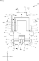
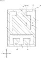
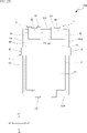
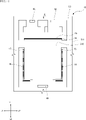
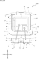
- FIG. FIG. 2 is a plan view of the semiconductor device shown in FIG. 1, and is a view through a sealing resin.
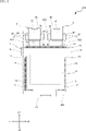
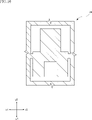
- 3 is a bottom view of the semiconductor device shown in FIG. 1.
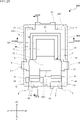
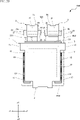
- FIG. FIG. 4 is a bottom view of the semiconductor device shown in FIG. 1, and is a view through the sealing resin.
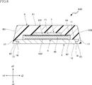
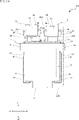
- FIG. 5 is a cross-sectional view along line VV in FIG.
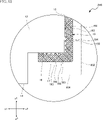
- FIG. 6 is a cross-sectional view taken along line VI-VI of FIG. 7 is a partially enlarged view of FIG. 6.
- FIG. 8 is a partially enlarged view of FIG. 4.
- FIG. 9 is a partially enlarged view of FIG. 4.
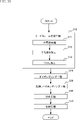
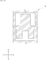
- FIG. 10 is a flow chart showing an example of a method for manufacturing the semiconductor device shown in FIG. 11A and 11B are plan views showing steps according to an example of a method of manufacturing the semiconductor device shown in FIG. 1.
- FIG. 12A and 12B are cross-sectional views showing steps according to an example of a method of manufacturing the semiconductor device shown in FIG. 13A and 13B are cross-sectional views showing steps according to an example of a method of manufacturing the semiconductor device shown in FIG. 14A and 14B are cross-sectional views showing steps according to an example of a method of manufacturing the semiconductor device shown in FIG.
- FIG. 15 is a bottom view showing a process according to an example of the method of manufacturing the semiconductor device shown in FIG.
- FIG. 1; 16A and 16B are plan views showing steps according to an example of a method of manufacturing the semiconductor device shown in FIG. 1.
- FIG. 17A and 17B are plan views showing steps according to an example of a method of manufacturing the semiconductor device shown in FIG.
- FIG. 18 is a plan view showing a process according to an example of the method of manufacturing the semiconductor device shown in FIG. 1;
- 19 is a bottom view of the semiconductor device according to the first modification of the first embodiment;
- FIG. 20 is a partially enlarged bottom view showing a semiconductor device according to a second modification of the first embodiment;
- FIG. 21 is a partially enlarged bottom view showing a semiconductor device according to a third modification of the first embodiment;
- FIG. 22 is a partially enlarged cross-sectional view showing a semiconductor device according to a second embodiment of the present disclosure
- 23A to 23C are cross-sectional views showing steps according to an example of a method of manufacturing the semiconductor device shown in FIG. 24 is a bottom view showing a semiconductor device according to a third embodiment of the present disclosure
- FIG. FIG. 25 is a plan view showing a semiconductor device according to a fourth embodiment of the present disclosure
- FIG. 26 is a plan view showing a semiconductor device according to a fifth embodiment of the present disclosure
- FIG. FIG. 27 is a perspective view showing a semiconductor device according to a sixth embodiment of the present disclosure
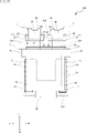
- FIG. 28 is a plan view of the semiconductor device shown in FIG. 27, and is a view through the sealing resin.
- FIG. 29 is a bottom view of the semiconductor device shown in FIG. 27.
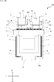
- FIG. FIG. 30 is a bottom view of the semiconductor device shown in FIG. 27, and is a view through the sealing resin.
- 31 is a cross-sectional view taken along line XXXI-XXXI of FIG. 28.
- FIG. 32 is a cross-sectional view taken along line XXXII-XXXII of FIG. 28.
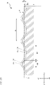
- FIG. 33 is a partially enlarged view of FIG. 32.
- FIG. 34 is a partially enlarged view of FIG. 30.
- FIG. 35 is a cross-sectional view taken along line XXXV-XXXV of FIG. 34.
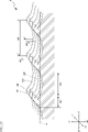
- FIG. 36 is a cross-sectional view taken along line XXVI-XXXVI of FIG. 34.
- FIG. FIG. 37 is a perspective view of an uneven portion.
- FIG. 38 is an SEM photograph of the uneven portion.
- 39 is a flow chart showing an example of a method for manufacturing the semiconductor device shown in FIG. 27.
- FIG. 40 is a plan view showing a process according to an example of the method of manufacturing the semiconductor device shown in FIG. 27.
- FIG. 41 is a bottom view showing a process according to an example of the method of manufacturing the semiconductor device shown in FIG. 27.
- FIG. FIG. 42 is a plan view showing a step according to an example of the method of manufacturing the semiconductor device shown in FIG. 27.
- FIG. FIG. 43 is a plan view showing a step according to an example of the method of manufacturing the semiconductor device shown in FIG. 27; FIG.
- FIG. 44 is a plan view showing a step according to an example of the method of manufacturing the semiconductor device shown in FIG. 27;
- FIG. 45 is a bottom view showing a semiconductor device according to the first modification of the sixth embodiment;
- FIG. 46 is a bottom view showing a semiconductor device according to a second modification of the sixth embodiment; 47 is a partially enlarged view of FIG. 46.
- FIG. FIG. 48 is a bottom view of a semiconductor device according to a third modification of the sixth embodiment; 49 is a partially enlarged view of FIG. 48.
- FIG. FIG. 50 is a bottom view showing a semiconductor device according to a fourth modification of the sixth embodiment; 51 is a partially enlarged view of FIG. 50.
- FIG. 52 is a partially enlarged bottom view showing a semiconductor device according to a fifth modification of the sixth embodiment; 53 is a partially enlarged bottom view showing a semiconductor device according to a sixth modification of the sixth embodiment; FIG. 54 is a partially enlarged bottom view showing a semiconductor device according to a seventh modification of the sixth embodiment; FIG. 55 is a bottom view showing the semiconductor device according to the seventh embodiment of the present disclosure; 56 is a partially enlarged cross-sectional view showing a semiconductor device according to an eighth embodiment of the present disclosure; FIG. 57 is a plan view showing a semiconductor device according to a ninth embodiment of the present disclosure; FIG. 58 is a plan view showing a semiconductor device according to a tenth embodiment of the present disclosure; FIG.
- FIG. 1 A semiconductor device A10 according to the first embodiment of the present disclosure will be described based on FIGS. 1 to 9.
- FIG. The semiconductor device A10 includes leads 1, leads 2, leads 3, a semiconductor element 6, connection leads 7, and a sealing resin 8. As shown in FIG.
- FIG. 1 is a perspective view showing the semiconductor device A10.
- FIG. 2 is a plan view showing the semiconductor device A10.
- the outer shape of the sealing resin 8 is shown by an imaginary line (chain double-dashed line) through the sealing resin 8.
- FIG. 3 is a bottom view showing the semiconductor device A10.
- FIG. 4 is a bottom view showing the semiconductor device A10.
- the outer shape of the sealing resin 8 is shown by an imaginary line (chain double-dashed line) through the sealing resin 8 .
- FIG. 5 is a cross-sectional view along line VV in FIG.
- FIG. 6 is a cross-sectional view taken along line VI-VI of FIG. 7 is a partially enlarged view of FIG. 6.
- FIG. 8 is a partially enlarged view of FIG. 4.
- FIG. 9 is a partially enlarged view of FIG. 4.
- the semiconductor device A10 shown in these figures is a device that is surface-mounted on circuit boards of various devices.
- the application and function of the semiconductor device A10 are not limited.
- the package format of the semiconductor device A10 is DFN (Dual Flatpack No-leaded). Note that the package format of the semiconductor device A10 is not limited to DFN.
- the shape of the semiconductor device A10 when viewed in the thickness direction is substantially rectangular.
- the thickness direction (planar view direction) of the semiconductor device A10 is defined as the z direction, and the direction along one side of the semiconductor device A10 orthogonal to the z direction (horizontal direction in FIGS.
- a direction orthogonal to the z-direction and the x-direction (vertical direction in FIGS. 2 to 4) is defined as the y-direction.
- One side in the z direction (the lower side in FIGS. 5 and 6) is the z1 side, and the other side (the upper side in FIGS. 5 and 6) is the z2 side.
- One side in the x direction (the left side in FIG. 2) is the x1 side, and the other side (the right side in FIG. 2) is the x2 side.
- One side in the y direction (the lower side in FIG. 2) is the y1 side, and the other side (the upper side in FIG. 2) is the y2 side.
- the z-direction corresponds to the "thickness direction" of the present disclosure.
- Each dimension of the semiconductor device A10 is not particularly limited, and in this embodiment, for example, the x-direction dimension is about 4 mm, the y-direction dimension is about 6 mm, and the z-direction dimension is about 1 mm.
- the leads 1 to 3 are electrically connected to the semiconductor element 6.
- the leads 1 to 3 are made of metal, preferably Cu or Ni, or an alloy thereof, 42 alloy, or the like. Note that the material of the leads 1 to 3 is not limited.
- the leads 1 to 3 are composed of a lead frame formed by stamping a metal plate, for example.
- the thickness of the leads 1 to 3 is not particularly limited, and is, for example, approximately 0.05 to 0.3 mm, and approximately 0.25 mm in this embodiment.
- the lead 1 is arranged at the end of the semiconductor device A10 on the y2 side in the y direction and spreads over the entire x direction.
- the lead 2 is arranged at a corner portion on the x-direction x1 side of the semiconductor device A10 on the y-direction y1 side.
- the lead 3 is arranged at a corner portion on the x-direction x2 side of the semiconductor device A10 on the y-direction y1 side. Leads 2 and 3 are spaced apart from lead 1 in the y-direction and are spaced apart from each other in the x-direction.
- the lead 1 supports the semiconductor element 6 and has a main surface 11 , a back surface 12 , an inner back surface 13 , an inner connecting surface 16 , an inner end surface 17 , and connecting end surfaces 14 and 15 .
- the main surface 11 and the back surface 12 face opposite to each other in the z direction.
- the main surface 11 faces the z-direction z2 side.
- the main surface 11 is a surface on which the semiconductor element 6 is mounted.
- the shape of the main surface 11 is substantially rectangular, and has portions that protrude on both sides in the y direction y2 and in the x direction. A part of each of these protruding portions is exposed and protrudes from the sealing resin 8 .
- the number of each projecting portion is not limited.
- the rear surface 12 is exposed from the sealing resin 8 and becomes a rear surface terminal.
- the shape of the back surface 12 is substantially rectangular, and has portions that protrude on both sides in the y direction y2 and in the x direction. A part of each of these protruding portions is exposed and protrudes from the sealing resin 8 . Note that the number of each projecting portion is not limited.
- the internal back surface 13 faces the same side as the back surface 12 in the z direction (z1 side in the z direction) and is covered with the sealing resin 8 .
- the inner back surface 13 is connected to the inner connecting surface 16 and the inner end surface 17 .
- the inner back surface 13 is formed on the y1 side, the y2 side in the y direction, the x1 side in the x direction, and the x2 side in the x direction of the back surface 12, respectively.
- the shape and arrangement position of the internal back surface 13 are not limited. As shown in FIGS.
- the thickness (dimension in the z direction) of the portion of the lead 1 where the inner back surface 13 is located is smaller than the thickness of the portion where the back surface 12 is located, for example about half.
- the inner back surface 13 is formed by crushing a part of the lead frame about half in the z-direction, as will be described later. The crushed portion of the leadframe extends radially outward. Therefore, the inner rear surface 13 has a rounded corner portion on the outer edge. As shown in FIGS. 3, 5, and 6, the inner rear surface 13 is not exposed from the sealing resin 8 and is covered with the sealing resin 8. As shown in FIGS. As a result, the leads 1 are prevented from falling out of the sealing resin 8 in the z direction z1.
- an uneven portion 19 is formed on the inner rear surface 13 .
- the concave-convex portion 19 is arranged over substantially the entire area of the inner back surface 13 .
- positioned is not limited. It is desirable that the region where the concave-convex portion 19 is arranged is wide, and that it is arranged at least on the outer edge portion of the inner rear surface 13 .
- the concave-convex portion 19 includes a plurality of concave portions 191 . As shown in FIG. 7, each recess 191 is recessed from the inner rear surface 13 toward the main surface 11 (z direction z2 side). Each concave portion 191 has a tapered shape in which the cross-sectional area on the xy plane becomes smaller toward the main surface 11 side (z direction z2 side). The shape of each concave portion 191 when viewed in the z-direction is a rectangular shape that is perpendicular to the z-direction and elongated in the extending direction (the x-direction in FIGS. 7 to 9) extending from the back surface 12 toward the outer edge of the inner back surface 13 .
- the plurality of recesses 191 are arranged in a matrix as shown in FIGS. 8 and 9 .
- a plurality of recesses 191 arranged at equal intervals in an orthogonal direction (y direction in FIGS. 7 to 9) perpendicular to the z direction and the extending direction are arranged in four rows in the extending direction. It is Note that the number of arrays is not limited.
- the plurality of recesses 191 each include a plurality of recesses 191a, 191b, 191c, and 191d.
- the plurality of recesses 191a are arranged at regular intervals along the y direction on the side closest to the rear surface 12 (the x1 side in the x direction in FIGS. 7 to 9).
- the plurality of recesses 191b are arranged at regular intervals along the y direction on the outer edge side of the plurality of recesses 191a (the x2 side in the x direction in FIGS. 7 to 9).
- the plurality of recesses 191c are arranged at equal intervals along the y direction on the outer edge side of the plurality of recesses 191b.
- the plurality of recesses 191d are arranged at equal intervals along the y direction on the outer edge side of the plurality of recesses 191c. In this embodiment, the recesses 191d extend to the outer edge of the inner back surface 13 .
- Each concave portion 191 has a larger dimension in the extending direction as it is arranged closer to the outer edge.
- the dimension L2 (see FIG. 8) in the extending direction of the recess 191d is larger than the dimension L1 (see FIG. 8) in the extending direction of the recess 191a.
- the plurality of recesses 191 are formed at the same time when the inner back surface 13 is formed by crushing, as will be described later.
- the recessed portion 191 positioned closer to the outer edge of the inner back surface 13 extends in the extending direction and the dimension in the extending direction becomes larger. ing. Moreover, since the crushed portion of the lead frame spreads radially at the end portion of the inner rear surface 13, the concave portion 191 has a curved and elongated shape as shown in FIG.
- the plurality of recesses 191 have substantially the same dimension L3 (see FIG. 8) in the orthogonal direction. Although the dimension L3 is not limited, it is about 10% or more and 30% or less of the dimension L4 (see FIG. 8) of the inner rear surface 13 in the extending direction. Further, the plurality of recesses 191 have substantially the same depth dimension (dimension in the z direction) D (see FIG. 7).
- the dimension D is, but not limited to, about 1% to 5% of the thickness dimension of the lead 1 (the dimension from the principal surface 11 to the back surface 12 in the z direction) T (see FIG. 7). In this embodiment, dimension D is about 5 to 10 ⁇ m.
- the plurality of recesses 191 have an arrangement, shape, and dimensions corresponding to the shape of an unevenness forming portion (described later) provided in the mold. Therefore, the plurality of recesses 191 can be formed with more precise arrangement, shape, and dimensions than when formed by laser or by half-etching, for example.
- the arrangement position, shape, and dimensions of each recess 191 are not limited.
- the inner connecting surface 16 is substantially orthogonal to the back surface 12 and the inner back surface 13 and is connected to the back surface 12 and the inner back surface 13 .
- the internal connection surface 16 is flat and covered with the sealing resin 8 .
- the inner end surface 17 is substantially perpendicular to the main surface 11 and the inner back surface 13 and connects to the main surface 11 and the inner back surface 13 .
- the inner end face 17 is covered with the sealing resin 8 .
- the connecting end surfaces 14 and 15 are surfaces orthogonal to the main surface 11 and the back surface 12 and are connected to the main surface 11 and the back surface 12 .
- the connecting end surfaces 14 and 15 are exposed from the sealing resin 8 .
- the connecting end surface 14 is connected to a portion of the main surface 11 protruding in the y direction y2 and a portion of the back surface 12 protruding in the y direction y2.
- the connecting end face 14 is formed with a concave portion that is concave in the y direction y1 and extends in the z direction.
- connecting end faces 15 There are two connecting end faces 15, one connecting end face 15 faces the x direction x1 side, and the other connecting end face 15 faces the x direction x2 side.
- the connecting end surface 15 facing the x-direction x1 side is connected to a portion of the main surface 11 protruding in the x-direction x1 side and a portion of the back surface 12 protruding in the x-direction x1 side.
- the connecting end surface 15 facing the x-direction x2 side is connected to a portion of the main surface 11 protruding in the x-direction x2 side and a portion of the rear surface 12 protruding in the x-direction x2 side.
- Each of the connecting end surfaces 14 and 15 is a cut surface formed by cutting a tie bar connected to the frame in the lead frame in a cutting step in the manufacturing process.
- the shape of the lead 1 is not limited to the one described above.
- a groove for preventing outflow of the bonding material may be formed on main surface 11 so as to surround semiconductor element 6 .
- the connecting end face 14 may not have a recess.
- the connecting end surfaces 14 and 15 may be flush with the surfaces of the sealing resin 8 instead of protruding from the sealing resin 8 .
- the shape of the lead 1 is appropriately designed according to the application and specifications.
- the lead 2 is electrically connected to the semiconductor element 6 and has a main surface 21 , a back surface 22 , an internal back surface 23 , an internal connection surface 26 , an internal end surface 27 and a connection end surface 24 .
- the main surface 21 and the back surface 22 face opposite sides in the z direction.
- the main surface 21 faces the same side as the main surface 11 of the lead 1 (z2 side in the z direction).
- the main surface 21 is the surface to which the connection lead 7 is joined.
- the shape of the main surface 21 is substantially rectangular.
- a portion of the main surface 21 on the y-direction y1 side is exposed from the sealing resin 8 and protrudes.
- the back surface 22 faces the same side as the back surface 12 of the lead 1 (z1 side in the z direction).
- the rear surface 22 is exposed from the sealing resin 8 and becomes a rear surface terminal.
- the shape of the back surface 22 is substantially rectangular.
- the internal back surface 23 faces the same side (z1 side in the z direction) as the back surface 22 in the z direction, and is covered with the sealing resin 8 .
- the inner back surface 23 is connected to an inner connecting surface 26 and an inner end surface 27 .
- the internal rear surface 23 is formed on the x-direction x1 side and the x-direction x2 side of the rear surface 22, respectively.
- the shape and arrangement position of the internal back surface 23 are not limited.
- the thickness (dimension in the z direction) of the portion of the lead 2 where the inner back surface 23 is located is smaller than the thickness of the portion where the back surface 22 is located, for example about half.
- the inner back surface 23 is also formed in the same manner as the inner back surface 13, the corners of the outer edge are rounded. As shown in FIG. 3 , the inner rear surface 23 is covered with the sealing resin 8 without being exposed from the sealing resin 8 . As a result, the leads 2 are prevented from falling out of the sealing resin 8 in the z direction z1.
- the internal connection surface 26 is substantially orthogonal to the back surface 22 and the internal back surface 23 and connects to the back surface 22 and the internal back surface 23 .
- the internal connection surface 26 is flat and covered with the sealing resin 8 .
- the inner end surface 27 is substantially perpendicular to the main surface 21 and the inner back surface 23 and connects to the main surface 21 and the inner back surface 23 .
- the inner end surface 27 is covered with the sealing resin 8 .
- the connecting end surface 24 is a surface perpendicular to the main surface 21 and the back surface 22 and is connected to the main surface 21 and the back surface 22 .
- the connecting end surface 24 is exposed from the sealing resin 8 .
- the connecting end surface 24 is recessed in the y direction y2 and has a recess extending in the z direction.
- the connecting end surface 24 is a cut surface formed by cutting tie bars connected to the frame in the lead frame in a cutting step in the manufacturing process.
- the shape of the lead 2 is not limited to the one described above.
- the connecting end face 24 may not have recesses.
- the connecting end surface 24 may not be located at a position protruding from the sealing resin 8 and may be flush with a resin side surface 833 (described later) of the sealing resin 8 .
- the shape of the lead 2 is appropriately designed according to the application and specifications.
- the lead 3 is conductive to the semiconductor element 6 and has a main surface 31 , a back surface 32 , an inner back surface 33 , an inner connecting surface 36 , an inner end surface 37 and a connecting end surface 34 .
- the main surface 31 and the back surface 32 face opposite sides in the z direction.
- the main surface 31 faces the same side as the main surface 11 of the lead 1 (z2 side in the z direction).
- the main surface 31 is the surface to which the connection lead 7 is joined.
- the shape of the main surface 31 is substantially rectangular.
- a portion of the main surface 31 on the y-direction y1 side is exposed from the sealing resin 8 and protrudes.
- the back surface 32 faces the same side as the back surface 12 of the lead 1 (z1 side in the z direction).
- the rear surface 32 is exposed from the sealing resin 8 and becomes a rear surface terminal.
- the shape of the back surface 32 is substantially rectangular.
- the internal back surface 33 faces the same side as the back surface 32 in the z direction (z1 side in the z direction) and is covered with the sealing resin 8 .
- the inner back surface 33 connects to an inner connecting surface 36 and an inner end surface 37 .
- the inner rear surface 33 is formed on the x-direction x1 side and the x-direction x2 side of the rear surface 32, respectively.
- the shape and arrangement position of the internal back surface 33 are not limited.
- the thickness (dimension in the z direction) of the portion of the lead 3 where the inner back surface 33 is located is smaller than the thickness of the portion where the back surface 32 is located, for example about half.
- the inner back surface 33 is also formed in the same manner as the inner back surface 13, the corners of the outer edge are rounded. As shown in FIG. 3 , the inner rear surface 33 is covered with the sealing resin 8 without being exposed from the sealing resin 8 . As a result, the leads 3 are prevented from falling out of the sealing resin 8 in the z direction z1.
- the inner connecting surface 36 is substantially orthogonal to the back surface 32 and the inner back surface 33 and is connected to the back surface 32 and the inner back surface 33 .
- the internal connection surface 36 is flat and covered with the sealing resin 8 .
- the inner end surface 37 is substantially orthogonal to the main surface 31 and the inner back surface 33 and connects to the main surface 31 and the inner back surface 33 .
- the inner end surface 37 is covered with the sealing resin 8 .
- the connecting end surface 34 is a surface perpendicular to the main surface 31 and the back surface 32 and is connected to the main surface 31 and the back surface 32 .
- the connecting end surface 34 is exposed from the sealing resin 8 .
- the connecting end surface 34 is recessed in the y direction y2 and has a recess extending in the z direction.
- the connecting end surface 34 is a cut surface formed by cutting tie bars connected to the frame in the lead frame in a cutting step in the manufacturing process.
- the shape of the lead 3 is not limited to the one described above.
- the connecting end face 34 may not have recesses.
- the connecting end surface 34 may be flush with a later-described resin side surface 833 of the sealing resin 8 instead of protruding from the sealing resin 8 .
- the shape of the lead 3 is appropriately designed according to the application and specifications.
- the semiconductor element 6 is an element that exerts electrical functions of the semiconductor device A10.
- the type of semiconductor element 6 is not particularly limited.
- the semiconductor element 6 is a diode.
- the semiconductor element 6 has an element body 60 , a first electrode 631 and a second electrode 632 .
- the element body 60 has a rectangular plate shape when viewed in the z direction.
- the element body 60 is made of a semiconductor material, and is made of Si (silicon) in this embodiment.
- the material of element body 60 is not limited, and may be other materials such as SiC (silicon carbide) and GaN (gallium nitride).
- the element body 60 has an element main surface 61 and an element back surface 62 .
- the element main surface 61 and the element back surface 62 face opposite to each other in the z direction.
- the element main surface 61 faces the z-direction z2 side.
- the element back surface 62 faces the z-direction z1 side.
- the first electrode 631 is arranged on the element main surface 61 .
- the second electrode 632 is arranged on the element back surface 62 . In this embodiment, the first electrode 631 is the anode electrode and the second electrode 632 is the cathode electrode.
- the semiconductor element 6 is bonded to the approximate center of the main surface 11 of the lead 1 via a bonding material (not shown).
- the bonding material is a conductive bonding material such as solder.
- the bonding material may be other conductive bonding materials such as silver paste and sintered silver bonding material.
- the semiconductor element 6 has the element rear surface 62 bonded to the main surface 11 of the lead 1 with a bonding material.
- a second electrode 632 of the semiconductor element 6 is conductively connected to the lead 1 via a bonding material.
- the lead 1 is conductively connected to the second electrode 632 (anode electrode) of the semiconductor element 6 and functions as an anode terminal.
- the first electrode 631 of the semiconductor element 6 is conductively connected to the leads 2 and 3 via the connection leads 7, as shown in FIGS.
- the leads 2 and 3 are conductively connected to the first electrode 631 (cathode electrode) of the semiconductor element 6 and function as a cathode terminal.
- the dimensions of the semiconductor element 6 in the x-direction and the y-direction are about 3 mm, which is relatively large compared to the leads 1 .
- the area S1 of the semiconductor element 6 viewed in the z-direction is about 60% of the area S2 of the lead 1 (the area of the main surface 11 of the lead 1) viewed in the z-direction.
- the area S1 is 50% or more of the area S2
- the area of the lead 1 in contact with the sealing resin 8 is small. Cracks are likely to occur in the sealing resin 8 .
- the inner back surface 13 is provided with the concave-convex portion 19, so that the semiconductor device A10 suppresses peeling of the sealing resin 8 on the inner back surface 13.
- connection lead 7 is a plate-shaped conductor that connects the semiconductor element 6 and the lead 2 and the lead 3 and conducts them.
- the connection lead 7 is formed by stamping or etching a metal plate.
- the connection lead 7 is made of metal, preferably one of Cu and Al, or an alloy thereof.
- the material of the connection lead 7 is not limited.
- the thickness of the connection lead 7 is not particularly limited, and is, for example, approximately 0.08 to 0.3 mm, and approximately 0.15 mm in this embodiment.
- the connection lead 7 is formed by bending a metal plate, and includes an element connection portion 71 , two lead connection portions 72 and a connecting portion 73 .
- the element connecting portion 71 is a portion that is connected to the semiconductor element 6, is substantially parallel to the xy plane, and has a substantially rectangular shape when viewed in the z direction.
- the element connection portion 71 is bonded to the first electrode 631 arranged on the element main surface 61 of the semiconductor element 6 via a bonding material (not shown).
- the bonding material is a conductive bonding material such as solder. Note that the bonding material is not limited.
- the two lead connection portions 72 are portions to be connected to the leads 2 and 3, respectively, and have an elongated rectangular shape that is substantially parallel to the xy plane and elongated in the x direction when viewed in the z direction.
- Each lead connection portion 72 is bonded to the principal surface 21 of the lead 2 or the principal surface 31 of the lead 3 via a bonding material (not shown).
- the bonding material is a conductive bonding material such as solder. Note that the bonding material is not limited.
- the connecting portion 73 is a portion that connects the element connecting portion 71 and the two lead connecting portions 72 .
- the connecting portion 73 is connected to the element connecting portion 71 at the end on the y2 side in the y direction.
- the end portion of the connecting portion 73 on the y-direction y1 side is divided into two pieces, each of which is connected to a different lead connecting portion 72 .
- the shape of the connection lead 7 is not limited.
- the first electrode 631 of the semiconductor element 6 may be connected to the lead 2 and the lead 3 by another connection member such as a bonding wire instead of the connection lead 7 .
- the encapsulating resin 8 partially covers each of the leads 1, 2, 3 and the semiconductor element 6 and the connection leads 7 as a whole.
- Sealing resin 8 is made of, for example, black epoxy resin.
- the material of the sealing resin 8 is not limited.
- the sealing resin 8 is formed, for example, by transfer molding using a mold. Note that the method for forming the sealing resin 8 is not limited.
- the sealing resin 8 has a resin main surface 81 , a resin back surface 82 and four resin side surfaces 83 .
- the resin main surface 81 and the resin back surface 82 face opposite sides in the z-direction.
- the resin main surface 81 is a surface facing the z-direction z2 side
- the resin back surface 82 is a surface facing the z-direction z1 side.
- the four resin side surfaces 83 are surfaces connected to the resin main surface 81 and the resin back surface 82, respectively. Each resin side surface 83 faces outward in the x direction or the y direction.
- the four resin sides 83 include a resin side 831 , a resin side 832 , a resin side 833 , and a resin side 834 .
- the resin side surface 831 and the resin side surface 832 face opposite sides in the x direction.
- the resin side surface 831 is a surface arranged on the x-direction x1 side and facing the x-direction x1 side.
- the resin side surface 832 is a surface arranged on the x-direction x2 side and facing the x-direction x2 side.
- the resin side surface 833 and the resin side surface 834 face opposite sides in the y direction.
- the resin side surface 833 is a surface arranged on the y-direction y1 side and facing the y-direction y1 side.
- the resin side surface 834 is a surface that is arranged on the y-direction y2 side and faces the y-direction y2 side.
- the four resin side surfaces 83 are inclined so as to approach each other toward the resin main surface 81 . That is, the sealing resin 8 has a tapered shape in which the cross-sectional area in the xy plane becomes smaller toward the resin main surface 81 .
- the shape of the sealing resin 8 shown in FIGS. 1 to 6 is an example. The shape of the sealing resin 8 is not limited to the illustrated shape.
- the back surface 12 of lead 1, the back surface 22 of lead 2, and the back surface 32 of lead 3 are exposed from resin back surface 82 of sealing resin 8, and are connected to resin back surface 82. are flush with each other.
- the connecting end surface 15 of the lead 1 facing the x-direction x1 side is exposed from the resin side surface 831 .
- the connecting end surface 15 of the lead 1 facing in the x direction x2 is exposed from the resin side surface 832 .
- the connection end surface 14 of the lead 1 is exposed from the resin side surface 834 .
- the connection end surface 24 of the lead 2 and the connection end surface 34 of the lead 3 are exposed from the resin side surface 833 .
- FIG. 10 An example of a method for manufacturing the semiconductor device A10 will be described below with reference to FIGS. 10 to 19.
- FIG. 10
- FIG. 10 is a flow chart showing an example of a method for manufacturing the semiconductor device A10.
- 11 to 19 are diagrams showing steps according to an example of a method of manufacturing the semiconductor device A10.
- 11 and 16 to 18 are plan views corresponding to FIG. 2.
- FIG. 12 to 14 are simplified cross-sectional views corresponding to cross-sectional views taken along line XII-XII in FIG. 15 is a bottom view, corresponding to FIG. 4.
- the method of manufacturing the semiconductor device A10 includes a lead frame forming step S10, a die bonding step S20, a connection lead bonding step S30, a sealing step S40, and a cutting step S50.
- the lead frame creation step S10 is a step of creating a lead frame from a metal plate.
- a metal plate that will be the material of the lead frame is prepared (S11).
- the metal plate has a main surface and a back surface facing opposite to each other in the z-direction.
- the lead frame 91 is formed by stamping the metal plate.
- a lead frame 91 is formed as shown in FIG. 11 by punching a metal plate (S12).
- the lead frame 91 is hatched.
- the lead frame 91 has a main surface 911 and a back surface 912 facing opposite to each other in the z-direction.
- a principal surface 911 of the lead frame 91 is a surface that becomes the principal surface 11 of the lead 1 , the principal surface 21 of the lead 2 , and the principal surface 31 of the lead 3 .
- the back surface 912 of the lead frame 91 is the back surface 12 of the lead 1 , the back surface 22 of the lead 2 , and the back surface 32 of the lead 3 .
- a through hole 92 is formed in a portion where the connecting end face 14 of the lead 1, the connecting end face 24 of the lead 2, and the connecting end face 34 of the lead 3 are formed.
- the lead frame 91 a plurality of portions that will become the semiconductor device A10 are connected to the frame 93, respectively. Note that FIG. 11 shows only a region that becomes one semiconductor device A10 (the same applies to FIGS. 15 and 18).
- Regions R are outer edge portions of portions of lead frame 91 that will become leads 1 to 3, and are relatively densely hatched portions on main surface 911 in FIG. 12 to 14 are diagrams for explaining the crushing process applied to the region R of the portion that will become the lead 1.
- FIG. 12 to 14 are simplified cross-sectional views taken along line XII-XII in FIG. As shown in FIGS. 12 to 14, the lead frame 91 is arranged with the main surface 911 in contact with the mold 96 . In FIGS. 12 to 14 as well, the region R is hatched with relatively dense hatching similar to that in FIG.
- a mold 95 is pressed against the region R of the lead frame 91 from the rear surface 912 side.
- the metal mold 95 has an irregularity forming portion 951 formed on the surface facing the back surface 912 .
- the concave-convex forming portion 951 includes a plurality of convex portions 952 that protrude in the z direction z2.
- Each projection 952 has the same shape and size.
- Each projection 952 has a rectangular shape when viewed in the z direction, and has a tapered shape in which the cross-sectional area on the xy plane becomes smaller toward the z direction z2 side.
- the plurality of protrusions 952 are arranged in a matrix at regular intervals in the x-direction and the y-direction.
- the convex portions 952 are arranged in four rows in the x direction. Note that the number of arrays is not limited. Also, the arrangement position, shape, and dimensions of each projection 952 are not limited.
- FIG. 12 shows a state in which the mold 95 is raised from the rear surface 912 side toward the region R of the lead frame 91 .
- the concave-convex forming part 951 of the mold 95 comes into contact with the rear surface 912, and the mold 95 is further raised as shown in FIG. That is, the unevenness forming portion 951 of the mold 95 is pressed against the region R of the lead frame 91 .
- the region R of the lead frame 91 is crushed by the mold 95 and expanded outward in the extending direction (x2 side in the x direction in FIG. 13).
- FIG. 14 shows a state in which the mold 95 is raised to a predetermined position.
- the region R is crushed and expanded by the mold 95 to form the inner back surface 13 .
- the inner back surface 13 faces the same side as the back surface 912 (the z1 side in the z direction) and is positioned closer to the main surface 911 than the back surface 912 in the z direction.
- the concave-convex portion 19 is formed in which the concave portions 191 are respectively arranged at positions corresponding to the plurality of convex portions 952 arranged in the concave-convex forming portion 951 .
- each recess 191 in the extending direction is larger than that of the lead frame 91 located outside because the region R of the lead frame 91 is crushed and extends outward in the extending direction.
- the inner end surface 17 is a surface that faces the outside in the extending direction of the crushed and expanded region R (the x2 side in the x direction in FIG. 14). Also, the portion that contacts the side surface of the mold 95 becomes the internal connection surface 16 .
- a region R of the lead frame 91 that will become the leads 2 and 3 is also crushed and expanded by the mold 95 to form the inner rear surfaces 23 and 33 .
- the concave-convex forming part 951 is not formed at the position facing the region R of the lead frame 91 where the leads 2 and 3 are to be formed. Therefore, the inner rear surfaces 23 and 33 are not formed with uneven portions.
- the main surface 911 and the back surface 912 of the lead frame 91 may be turned upside down, and the mold 95 may be lowered to press the concave/convex portion 951 from the back surface 912 side of the lead frame 91 .
- a lead frame 94 is prepared as shown in FIG. In FIG. 16, the lead frame 94 is hatched.
- the lead frame 94 is a plate-shaped material that becomes the connection leads 7 . Note that FIG. 16 shows only a region that becomes one connection lead 7 (the same applies to FIG. 17).
- the lead frame 94 is formed by stamping or etching a metal plate.
- the lead frame 94 is bent to form an element connecting portion 71, two lead connecting portions 72, and a connecting portion 73.
- the connection lead 7 is obtained by cutting the lead frame 94 along the cutting line (indicated by the dashed line in FIG. 17).
- the die bonding step S20 is a step of bonding the semiconductor element 6 to the lead frame 91.
- solder paste is first applied to the center of the main surface 911 of the lead frame 91 that will become the main surface 11 of the lead 1 .
- the semiconductor element 6 is placed on the applied solder paste.
- a reflow process is performed to melt and then solidify the solder paste.
- the semiconductor element 6 is joined to the lead frame 91 .
- the bonding method of the semiconductor element 6 in the die bonding step S20 is not limited.
- connection lead bonding step S30 is a step of bonding the connection lead 7, as shown in FIG.
- solder paste is applied to the first electrodes 631 on the main surface 61 of the semiconductor element 6 .
- Solder paste is also applied to a region of the main surface 911 of the lead frame 91 that will become the main surface 21 of the lead 2 and a region that will become the main surface 31 of the lead 3 .
- the connection leads 7 are then mounted on the semiconductor element 6 and the lead frame 91 .
- the element connection portion 71 of the connection lead 7 is arranged on the solder paste applied to the first electrode 631 of the semiconductor element 6 .
- connection lead 7 is placed on the solder paste applied to the area that will become the main surface 21 of the lead 2 , and the other lead connection portion 72 is applied to the area that will become the main surface 31 of the lead 3 . It is placed on top of the solder paste. Then, a reflow process is performed to melt and then solidify the solder paste. As a result, the element connecting portion 71 and the first electrode 631 are joined by soldering, the lead connecting portion 72 on one side is joined to the region of the main surface 21 of the lead 2 , and the lead connecting portion 72 on the other side is joined to the lead 3 . is joined to the area that will become the main surface 31 of the .
- the bonding method of the connection lead 7 in the connection lead bonding step S30 is not limited.
- the sealing step S40 is a step of forming the sealing resin 8.
- a resin material is cured to form a sealing resin 8 (indicated by a chain double-dashed line in FIG. 18) that covers a portion of the lead frame 91, the semiconductor element 6, and the connection leads 7.
- the process is performed, for example, by well-known transfer molding using a mold. Specifically, the lead frame 91 to which the semiconductor element 6 and the connection leads 7 are joined is set in a molding machine. Next, the fluidized resin material is poured into a cavity in a mold for molding. Then, the resin material is cured. As described above, the sealing resin 8 is formed.
- the back surface 912 of the lead frame 91 is exposed from the sealing resin 8 by setting the lead frame 91 with the back surface 912 in contact with the mold. Further, the rear surface 912 of the lead frame 91 and the resin rear surface 82 of the sealing resin 8 are flush with each other. Moreover, since the resin material flows between the mold and the inner back surfaces 13 , 23 , 33 , the inner back surfaces 13 , 23 , 33 are covered with the sealing resin 8 .
- the method for forming the sealing resin 8 in the sealing step S40 is not limited.
- the cutting step S50 is a step of cutting the lead frame 91 .
- a blade is used to cut the lead frame 91 along cutting lines (indicated by dashed-dotted lines in FIG. 18) to separate the lead frames 91 into individual pieces.
- an individual piece to be the semiconductor device A10 is formed.
- the lead frame 91 is cut into leads 1 , 2 and 3 .
- the cut surfaces formed at this time become the connecting end surfaces 14 and 15 of the lead 1, the connecting end surface 24 of the lead 2, and the connecting end surface 34 of the lead 3.
- the through holes 92 form recesses in the connecting end surface 14 , the connecting end surface 24 and the connecting end surface 34 .
- the cutting method in the cutting step S50 is not limited. Through the above steps, the semiconductor device A10 described above is manufactured.
- the inner back surface 13 of the lead 1 is formed with an uneven portion 19 .
- the concave-convex portion 19 has a plurality of concave portions 191 . Since the contact area between the inner rear surface 13 and the sealing resin 8 is larger than when the uneven portion 19 is not formed, the adhesion of the sealing resin 8 to the inner rear surface 13 is improved. Thereby, the semiconductor device A10 can suppress peeling of the sealing resin 8 on the inner back surface 13 .
- the plurality of recesses 191 are arranged in a matrix.
- the plurality of recesses 191 are formed by stamping. Therefore, the plurality of recesses 191 can be formed with more precise arrangement, shape, and dimensions than when formed by laser or by half-etching, for example.
- the manufacturing process of the semiconductor device A10 can be simplified as compared with the case of forming the plurality of concave portions 191 by other methods, so that the manufacturing time can be shortened and the manufacturing cost can be suppressed.
- FIG. 19 is a bottom view showing the semiconductor device A11 according to the first modification of the first embodiment, which corresponds to FIG.
- the outer shape of the sealing resin 8 is shown by imaginary lines (chain lines) as seen through the sealing resin 8 .
- the semiconductor device A11 has a narrower range in which the uneven portion 19 is formed on the inner back surface 13 compared to the semiconductor device A10.
- the uneven portion 19 is formed only on the outer edge portion of the inner back surface 13 .
- the range in which the concave-convex portion 19 is formed on the inner rear surface 13 is not limited.
- the uneven portion 19 is desirably formed at least on the outer edge of the inner back surface 13 , and more preferably formed over the entire area of the inner back surface 13 .
- FIG. 20 is a diagram for explaining the semiconductor device A12 according to the second modification of the first embodiment.
- FIG. 20 is a partially enlarged bottom view of the semiconductor device A12, corresponding to FIG.
- the semiconductor device A12 differs from the semiconductor device A10 in the method of arranging the plurality of concave portions 191 in the uneven portion 19 .
- a plurality of recesses 191 are arranged in a checkered pattern.
- the arrangement method of the plurality of recesses 191 in the uneven portion 19 is not limited, and the plurality of recesses 191 may be arranged, for example, at random.
- the arrangement positions of the plurality of concave portions 191 in the uneven portion 19 can be appropriately set by the arrangement of the plurality of convex portions 952 in the uneven forming portion 951 of the mold 95 .
- FIG. 21 is a diagram for explaining the semiconductor device A13 according to the third modification of the first embodiment.
- FIG. 21 is a partially enlarged bottom view showing the semiconductor device A13, corresponding to FIG.
- the semiconductor device A13 differs from the semiconductor device A10 in the z-direction shape of each recess 191 in the uneven portion 19 .
- the shape of each recess 191 in the z-direction is circular or elliptical.
- Each concave portion 191 has a larger dimension in the extending direction (the x direction in FIG. 21) as it is arranged closer to the outer edge.
- each concave portion 191 in the concave/convex portion 19 when viewed in the z-direction is not limited, and may be other shapes. Also, the shape of each recess 191 may be different.
- the shape of each concave portion 191 in the concave-convex portion 19 can be appropriately set according to the shape of each convex portion 952 in the concave-convex forming portion 951 of the mold 95 .
- the uneven portions 19 are formed on all of the portions of the inner back surface 13 that are arranged on both sides of the back surface 12 in the x direction and the portions of the inner back surface 13 that are arranged on both sides of the back surface 12 in the y direction.
- the inner back surface 13 may have a portion where the concave-convex portion 19 is not formed.
- the concave-convex portion 19 may not be formed on a portion of the inner back surface 13 sufficiently distant from the semiconductor element 6 .
- FIG. 22 and 23 are diagrams for explaining the semiconductor device A20 according to the second embodiment of the present disclosure.
- FIG. 22 is a partially enlarged cross-sectional view showing the semiconductor device A20, corresponding to FIG.
- FIG. 23 is a cross-sectional view showing a process according to an example of the method of manufacturing the semiconductor device A20, and corresponds to FIG.
- the semiconductor device A20 according to the present embodiment differs from the semiconductor device A10 according to the first embodiment in that the uneven portion 19 includes a plurality of convex portions 192 .
- the configuration and operation of other portions of this embodiment are the same as those of the first embodiment.
- each part of said 1st Embodiment and each modification may be combined arbitrarily.
- the concave-convex portion 19 formed on the inner rear surface 13 of the lead 1 according to the present embodiment has a plurality of convex portions 192 instead of the plurality of concave portions 191 .
- each projection 192 protrudes from the internal back surface 13 toward the back surface 12 (the z-direction z1 side).
- Each convex portion 192 has a tapered shape in which the cross-sectional area on the xy plane increases toward the main surface 11 side (z direction z2 side).
- the shape of each convex portion 192 when viewed in the z-direction is a rectangular shape elongated in the extending direction (the x-direction in FIG. 22), like the concave portion 191 according to the first embodiment.
- the plurality of protrusions 192 are arranged in a matrix.
- the plurality of protrusions 192 are formed on the inner back surface 13 by crushing using a mold 95 having an unevenness forming portion 951 having a plurality of recesses 953 recessed in the z direction z1 side. sometimes formed at the same time.
- an uneven portion 19 is formed on the inner back surface 13 of the lead 1 .
- the concave-convex portion 19 includes a plurality of convex portions 192 . Therefore, the adhesion of the sealing resin 8 to the inner rear surface 13 is improved. Thereby, the semiconductor device A20 can suppress peeling of the sealing resin 8 on the inner back surface 13 . Moreover, the semiconductor device A20 has the same effect as the semiconductor device A10 due to the configuration common to the semiconductor device A10.
- FIG. 24 is a diagram for explaining the semiconductor device A30 according to the third embodiment of the present disclosure.
- FIG. 24 is a bottom view of the semiconductor device A30, corresponding to FIG. In FIG. 24, for convenience of understanding, the outer shape of the sealing resin 8 is shown by an imaginary line (double-dot chain line) through the sealing resin 8 .
- the semiconductor device A30 according to the present embodiment is different from the semiconductor device according to the first embodiment in that the uneven portions 29 are formed on the inner rear surface 23 of the lead 2 and the uneven portions 39 are formed on the inner rear surface 33 of the lead 3 . Different from A10.
- the configuration and operation of other portions of this embodiment are the same as those of the first embodiment. It should be noted that each part of the above-described first and second embodiments and modifications may be combined arbitrarily.
- an uneven portion 29 is formed on the inner rear surface 23 of the lead 2 according to this embodiment. Further, an uneven portion 39 is formed on the inner rear surface 33 of the lead 3 according to this embodiment.
- the configurations of the uneven portion 29 and the uneven portion 39 are similar to the configuration of the uneven portion 19 of the semiconductor device A10 according to the first embodiment.
- the configurations of the uneven portion 29 and the uneven portion 39 are not limited, and may be the same configuration as each modification of the uneven portion 19 according to the first embodiment.
- the uneven portion 29 and the uneven portion 39 are formed by forming the uneven portion 951 also at the position facing the region R of the lead frame 91 where the leads 2 and 3 are to be formed.
- an uneven portion 19 is formed on the inner back surface 13 of the lead 1 .
- the concave-convex portion 19 has a plurality of concave portions 191 . Therefore, the adhesion of the sealing resin 8 to the inner rear surface 13 is improved. Thereby, the semiconductor device A30 can suppress peeling of the sealing resin 8 on the inner back surface 13 . Further, the semiconductor device A30 has the same effect as the semiconductor device A10 due to the configuration common to the semiconductor device A10. Furthermore, according to the present embodiment, the inner rear surface 23 is formed with the uneven portion 29 and the inner rear surface 33 is formed with the uneven portion 39 . Thereby, the semiconductor device A30 can also suppress peeling of the sealing resin 8 on the inner back surface 23 and the inner back surface 33 .
- FIG. 25 is a diagram for explaining a semiconductor device A40 according to the fourth embodiment of the present disclosure.
- FIG. 25 is a plan view showing the semiconductor device A40, corresponding to FIG.
- the semiconductor device A40 according to the present embodiment differs from the semiconductor device A10 according to the first embodiment in that wires 79 are provided instead of the connection leads 7.
- FIG. The configuration and operation of other portions of this embodiment are the same as those of the first embodiment. It should be noted that each part of the above-described first to third embodiments and modifications may be arbitrarily combined.
- the semiconductor device A40 does not have connection leads 7, but has two wires 79 instead.
- One wire 79 is joined to the first electrode 631 of the semiconductor element 6 and the main surface 21 of the lead 2 .
- the other wire 79 is joined to the first electrode 631 of the semiconductor element 6 and the main surface 31 of the lead 3 .
- the number of wires 79 connecting the first electrode 631 and the main surface 21 and the number of the wires 79 connecting the first electrode 631 and the main surface 31 are not limited to one.
- Each may be connected with multiple wires 79 .
- the material and diameter of each wire 79 are not limited.
- an uneven portion 19 is formed on the inner back surface 13 of the lead 1 .
- the concave-convex portion 19 has a plurality of concave portions 191 . Therefore, the adhesion of the sealing resin 8 to the inner rear surface 13 is improved. Thereby, the semiconductor device A40 can suppress peeling of the sealing resin 8 on the inner back surface 13 .
- the semiconductor device A40 has the same effect as the semiconductor device A10 due to the configuration common to the semiconductor device A10. Furthermore, according to this embodiment, it is not necessary to prepare the connection lead 7 . Therefore, the semiconductor device A40 can simplify the manufacturing process and reduce the manufacturing cost.
- FIG. 26 is a diagram for explaining a semiconductor device A50 according to the fifth embodiment of the present disclosure.
- FIG. 26 is a plan view showing the semiconductor device A50, corresponding to FIG.
- the semiconductor device A50 according to the present embodiment differs from the semiconductor device A10 according to the first embodiment in the type of the semiconductor element 6, and is provided with wires 79 instead of the connection leads 7. This is different from the semiconductor device A10.
- the configuration and operation of other portions of this embodiment are the same as those of the first embodiment. It should be noted that each part of the above-described first to fourth embodiments and modifications may be combined arbitrarily.
- the semiconductor element 6 is, for example, a MOSFET (metal-oxide-semiconductor field-effect transistor).
- the semiconductor element 6 may be another transistor such as an IGBT (Insulated Gate Bipolar Transistor).
- the semiconductor element 6 further includes a third electrode 633 arranged on the element main surface 61 .
- the first electrode 631 is the source electrode
- the second electrode 632 is the drain electrode
- the third electrode 633 is the gate electrode.
- a second electrode 632 of the semiconductor element 6 is conductively connected to the lead 1 via a bonding material. Thereby, the lead 1 is conductively connected to the second electrode 632 (drain electrode) of the semiconductor element 6 and functions as a drain terminal.
- a first electrode 631 of the semiconductor element 6 is conductively connected to the lead 2 via a wire 79 .
- the lead 2 is conductively connected to the first electrode 631 (source electrode) of the semiconductor element 6 and functions as a source terminal.
- a third electrode 633 of the semiconductor element 6 is conductively connected to the lead 3 via a wire 79 .
- the lead 3 is conductively connected to the third electrode 633 (gate electrode) of the semiconductor element 6 and functions as a gate terminal.
- an uneven portion 19 is formed on the inner back surface 13 of the lead 1 .
- the concave-convex portion 19 has a plurality of concave portions 191 . Therefore, the adhesion of the sealing resin 8 to the inner rear surface 13 is improved. Thereby, the semiconductor device A50 can suppress peeling of the sealing resin 8 on the inner back surface 13 . Moreover, the semiconductor device A50 has the same effect as the semiconductor device A10 due to the configuration common to the semiconductor device A10.
- first electrode 631 and the lead 2 are conductively connected by the wire 79 and the third electrode 633 and the lead 3 are conductively connected by the wire 79 has been described, but the present invention is not limited to this. Absent.
- the first electrode 631 and the lead 2, and the third electrode 633 and the lead 3 may be conductively connected by other connection members such as connection leads.
- the semiconductor element 6 is a diode
- the semiconductor element 6 is a transistor
- the present invention is not limited to these.
- the type of semiconductor element 6 is not limited, and other semiconductor elements such as integrated circuits may be used.
- the case where three leads are arranged has been described, but the present invention is not limited to this.
- the number and arrangement positions of the leads to be arranged are not limited, and are appropriately set according to the number and arrangement positions of the electrodes arranged on the element main surface 61 of the semiconductor element 6 .
- FIG. A semiconductor device A60 includes leads 1, leads 2, leads 3, a semiconductor element 6, connection leads 7, and a sealing resin 8. As shown in FIG.
- FIG. 27 is a perspective view showing the semiconductor device A60.
- FIG. 28 is a plan view showing the semiconductor device A60.
- the outer shape of the sealing resin 8 is shown by an imaginary line (double-dot chain line) through the sealing resin 8 .
- FIG. 29 is a bottom view showing the semiconductor device A60.
- FIG. 30 is a bottom view showing the semiconductor device A60.
- the outer shape of the sealing resin 8 is shown by an imaginary line (chain double-dashed line) through the sealing resin 8.
- FIG. 31 is a cross-sectional view taken along line XXXI-XXXI of FIG. 28.
- FIG. 32 is a cross-sectional view taken along line XXXII-XXXII of FIG. 28.
- FIG. 33 is a partially enlarged view of FIG. 32.
- FIG. 34 is a partially enlarged view of FIG. 30.
- FIG. 35 is a cross-sectional view taken along line XXXV-XXXV of FIG. 34.
- FIG. 36 is a cross-sectional view taken along line XXXVI-XXXVI of FIG. 34.
- FIG. 37 is a perspective view of the uneven portion 19.
- FIG. 35 to 37 are schematic diagrams for explaining the shape of the uneven portion 19.
- FIG. FIG. 38 is an SEM photograph of the uneven portion 19 taken using a scanning electron microscope (SEM).
- the semiconductor device A60 shown in these figures is a device that is surface-mounted on circuit boards of various devices. Note that the application and function of the semiconductor device A60 are not limited.
- the package format of the semiconductor device A60 is DFN (Dual Flatpack No-leaded). Note that the package format of the semiconductor device A60 is not limited to DFN.
- the shape of the semiconductor device A60 when viewed in the thickness direction is substantially rectangular. For convenience of explanation, the thickness direction (planar view direction) of the semiconductor device A60 is defined as the z direction, and the direction along one side of the semiconductor device A60 orthogonal to the z direction (horizontal direction in FIGS.
- a direction orthogonal to the z-direction and the x-direction (vertical direction in FIGS. 28 to 30) is defined as the y-direction.
- One side in the z direction (the lower side in FIGS. 31 and 32) is the z1 side, and the other side (the upper side in FIGS. 31 and 32) is the z2 side.
- One side in the x direction (the left side in FIG. 28) is the x1 side, and the other side (the right side in FIG. 28) is the x2 side.
- One side in the y direction (the lower side in FIG. 28) is the y1 side, and the other side (the upper side in FIG. 28) is the y2 side.
- the z-direction corresponds to the "thickness direction" of the present disclosure.
- Each dimension of the semiconductor device A60 is not particularly limited, and in this embodiment, for example, the x-direction dimension is about 4 mm, the y-direction dimension is about 6 mm, and the z-direction dimension is about 1 mm.
- the leads 1 to 3 are electrically connected to the semiconductor element 6.
- the leads 1 to 3 are made of metal, preferably Cu or Ni, or an alloy thereof, 42 alloy, or the like. Note that the material of the leads 1 to 3 is not limited.
- the leads 1 to 3 are composed of a lead frame formed by stamping a metal plate, for example.
- the thickness of the leads 1 to 3 is not particularly limited, and is, for example, 0.05 to 0.3 mm, and in this embodiment is about 0.25 mm.
- the lead 1 is arranged at the end of the semiconductor device A60 on the y2 side in the y direction and spreads all over in the x direction.
- the lead 2 is arranged at a corner portion on the x-direction x1 side of the semiconductor device A60 on the y-direction y1 side.
- the lead 3 is arranged at a corner portion on the x-direction x2 side of the semiconductor device A60 on the y-direction y1 side. Leads 2 and 3 are spaced apart from lead 1 in the y-direction and are spaced apart from each other in the x-direction.
- the lead 1 supports the semiconductor element 6 and has a main surface 11 , a back surface 12 , an inner back surface 13 , an inner connecting surface 16 , an inner end surface 17 , and connecting end surfaces 14 and 15 .
- the main surface 11 and the back surface 12 face opposite to each other in the z direction.
- the main surface 11 faces the z-direction z2 side.
- the main surface 11 is a surface on which the semiconductor element 6 is mounted.
- the shape of the main surface 11 is substantially rectangular, and has portions that protrude on both sides in the y direction y2 and in the x direction. A part of each of these protruding portions is exposed and protrudes from the sealing resin 8 .
- the number of each projecting portion is not limited.
- the rear surface 12 is exposed from the sealing resin 8 and becomes a rear surface terminal.
- the shape of the back surface 12 is substantially rectangular, and has portions that protrude on both sides in the y direction y2 and in the x direction. A part of each of these protruding portions is exposed and protrudes from the sealing resin 8 . Note that the number of each projecting portion is not limited.
- the internal back surface 13 faces the same side as the back surface 12 in the z direction (z1 side in the z direction) and is covered with the sealing resin 8 .
- the inner back surface 13 is connected to the inner connecting surface 16 and the inner end surface 17 .
- the inner back surface 13 is formed on the y1 side, the y2 side, the x1 side, and the x2 side of the back surface 12 in the y direction.
- the shape and arrangement position of the internal back surface 13 are not limited.
- the thickness (dimension in the z direction) of the portion of the lead 1 where the inner back surface 13 is located is smaller than the thickness of the portion where the back surface 12 is located, for example about half.
- the inner back surface 13 is formed by stamping when forming a lead frame from a metal plate. As shown in FIGS. 29, 31, and 32, the inner rear surface 13 is not exposed from the sealing resin 8 and is covered with the sealing resin 8. As shown in FIGS. As a result, the leads 1 are prevented from falling out of the sealing resin 8 in the z direction z1.
- an uneven portion 19 is formed on the inner rear surface 13 .
- the concave-convex portion 19 is arranged on almost the entire area of the inner back surface 13 except for the portion connected to the inner connecting surface 16 .
- positioned is not limited. It is desirable that the region where the concave-convex portion 19 is arranged is wide, and that it is arranged at least on the outer edge portion of the inner rear surface 13 .
- the uneven portion 19 is formed by irradiating the inner rear surface 13 with a laser, as will be described later.
- the uneven portion 19 has a plurality of first protrusions 193 and a plurality of first recesses 194 .
- each first convex portion 193 protrudes from the periphery toward the back surface 12 (z1 side in the z direction).
- 35 to 37) is located on the z-direction z1 side of the imaginary line a (indicated by a two-dot chain line in FIGS. 35 to 37).
- Each first recess 194 is recessed with respect to each first protrusion 193 on the side facing the main surface 11 (z direction z2 side), and is located on the z direction z2 side of the imaginary line a in the uneven portion 19. This is the part to do.
- the plurality of first protrusions 193 and the plurality of first recesses 194 are formed by irradiating the inner back surface 13 with a laser.
- the scanning direction of the laser is the x-direction, so as shown in FIGS. 34, 37, and 38, the plurality of first concave portions 194 extend in the x-direction.
- scanning in the x direction is repeated while moving the laser irradiation position in the y direction, so a plurality of first concave portions 194 are formed side by side in the y direction.
- the first concave portion 194 is stippled for convenience of understanding.
- the portions between the adjacent first concave portions 194 become the first convex portions 193, so the plurality of first convex portions 193 also extend in the x direction and are formed side by side in the y direction.
- the dimension T1 (see FIG. 35) of the unevenness difference which is the dimension in the z direction from the bottom of the first concave portion 194 to the top of the first convex portion 193, can be adjusted by the output of the laser.
- Dimension T1 is, but not limited to, sufficiently smaller than T2 (see FIGS. 33 and 35) of thickness of lead 1 (dimension from main surface 11 to rear surface 12 in the z direction), and is 1% or more and 5% or less. degree. In this embodiment, the dimension T1 is approximately 3 ⁇ m.
- the y-direction dimension of the first concave portion 194 is adjustable by the output of the laser, and is not particularly limited. Also, the dimension of the first projection 193 in the y direction is adjustable by adjusting the laser irradiation interval, and is not particularly limited.
- each first recess 194 has a plurality of second protrusions 195 and a plurality of second recesses 196 formed therein.
- Each of the second protrusions 195 protrudes from the periphery toward the back surface 12 (z1 side in the z direction). is the part located in Each second recess 196 is recessed with respect to each second protrusion 195 toward the main surface 11 (z2 side in the z direction). This is a portion located on the z-direction z2 side of the normal position.
- the laser that forms the concave-convex portion 19 is irradiated with a pulse output that periodically repeats ON and OFF.
- a second concave portion 196 is formed when the pulse output is on, and a second convex portion 195 is formed when the pulse output is off. Therefore, the plurality of second protrusions 195 and the plurality of second recesses 196 are regularly arranged in the x direction.
- a second concave portion 196 is arranged between adjacent second convex portions 195 .
- a dimension T3 (see FIG. 35) of the unevenness difference which is the dimension in the z direction from the bottom of the second concave portion 196 to the top of the second convex portion 195, can be adjusted by the output of the laser. Although the dimension T3 is not limited, in this embodiment, it is smaller than the dimension T1 and about 25% or less of the dimension T1.
- the interval W2 (see FIGS.
- the interval W2 is not limited, in the present embodiment, it is smaller than the interval W1 (see FIGS. 35 and 37) between adjacent first protrusions 193 in the y direction, and is about 20% or less of the interval W1. In this embodiment, the interval W1 is approximately 30 ⁇ m, while the interval W2 is approximately 5 ⁇ m.
- each first protrusion 193 has a plurality of second protrusions 197 and a plurality of third recesses 198 formed therein.
- Each of the second protrusions 197 protrudes from the periphery toward the back surface 12 (z1 side in the z direction). This is the part located on the z1 side.
- Each third recess 198 is recessed with respect to each second protrusion 197 toward the main surface 11 (z direction z2 side). is located on the z-direction z2 side of the average position in .
- the plurality of second convex portions 197 and the plurality of third concave portions 198 are formed by pulse output of the laser that forms the uneven portion 19 .
- the plurality of second protrusions 197 and the plurality of third recesses 198 are regularly arranged in the x direction.
- a third concave portion 198 is arranged between adjacent second convex portions 197 .
- the dimension T4 (see FIG. 35) of the unevenness difference which is the dimension in the z direction from the bottom of the third concave portion 198 to the top of the second convex portion 197, is not limited, but is smaller than the dimension T1 and about 25% or less of the dimension T1. is.
- the interval W3 (see FIGS. 36 and 37) between adjacent second protrusions 197 in the x direction is approximately the same as the interval W2.
- the inner connecting surface 16 is substantially orthogonal to the back surface 12 and the inner back surface 13 and is connected to the back surface 12 and the inner back surface 13 .
- the internal connection surface 16 is covered with the sealing resin 8 .
- the inner end surface 17 is substantially perpendicular to the main surface 11 and the inner back surface 13 and connects to the main surface 11 and the inner back surface 13 .
- the inner end face 17 is covered with the sealing resin 8 .
- the connecting end surfaces 14 and 15 are surfaces orthogonal to the main surface 11 and the back surface 12 and are connected to the main surface 11 and the back surface 12 .
- the connecting end surfaces 14 and 15 are exposed from the sealing resin 8 .
- the connecting end surface 14 is connected to a portion of the main surface 11 protruding in the y direction y2 and a portion of the back surface 12 protruding in the y direction y2.
- the connecting end face 14 is formed with a concave portion that is concave in the y direction y1 and extends in the z direction.
- connecting end faces 15 There are two connecting end faces 15, one connecting end face 15 faces the x direction x1 side, and the other connecting end face 15 faces the x direction x2 side.
- the connecting end surface 15 facing the x-direction x1 side is connected to a portion of the main surface 11 protruding in the x-direction x1 side and a portion of the back surface 12 protruding in the x-direction x1 side.
- the connecting end surface 15 facing the x-direction x2 side is connected to a portion of the main surface 11 protruding in the x-direction x2 side and a portion of the rear surface 12 protruding in the x-direction x2 side.
- Each of the connecting end surfaces 14 and 15 is a cut surface formed by cutting a tie bar connected to the frame in the lead frame in a cutting step in the manufacturing process.
- the shape of the lead 1 is not limited to the one described above.
- a groove for preventing outflow of the bonding material may be formed on main surface 11 so as to surround semiconductor element 6 .
- the connecting end face 14 may not have a recess.
- the connecting end surfaces 14 and 15 may be flush with the surfaces of the sealing resin 8 instead of protruding from the sealing resin 8 .
- the shape of the lead 1 is appropriately designed according to the application and specifications.
- the lead 2 is electrically connected to the semiconductor element 6 and has a main surface 21 , a back surface 22 , an internal back surface 23 , an internal connection surface 26 , an internal end surface 27 and a connection end surface 24 .
- the main surface 21 and the back surface 22 face opposite sides in the z direction.
- the main surface 21 faces the same side as the main surface 11 of the lead 1 (z2 side in the z direction).
- the main surface 21 is the surface to which the connection lead 7 is joined.
- the shape of the main surface 21 is substantially rectangular.
- a portion of the main surface 21 on the y-direction y1 side is exposed from the sealing resin 8 and protrudes.
- the back surface 22 faces the same side as the back surface 12 of the lead 1 (z1 side in the z direction).
- the rear surface 22 is exposed from the sealing resin 8 and becomes a rear surface terminal.
- the shape of the back surface 22 is substantially rectangular.
- the internal back surface 23 faces the same side (z1 side in the z direction) as the back surface 22 in the z direction, and is covered with the sealing resin 8 .
- the inner back surface 23 is connected to an inner connecting surface 26 and an inner end surface 27 .
- the inner rear surface 23 is formed on the x-direction x1 side and the x-direction x2 side of the rear surface 22, respectively.
- the shape and arrangement position of the internal back surface 23 are not limited.
- the thickness (dimension in the z direction) of the portion of the lead 2 where the inner back surface 23 is located is smaller than the thickness of the portion where the back surface 22 is located, for example about half.
- the inner back surface 23 is formed by stamping when forming a lead frame from a metal plate. As shown in FIG. 29 , the inner rear surface 23 is covered with the sealing resin 8 without being exposed from the sealing resin 8 . As a result, the leads 2 are prevented from falling out of the sealing resin 8 in the z direction z1.
- the internal connection surface 26 is substantially orthogonal to the back surface 22 and the internal back surface 23 and connects to the back surface 22 and the internal back surface 23 .
- the internal connection surface 26 is covered with the sealing resin 8 .
- the inner end surface 27 is substantially perpendicular to the main surface 21 and the inner back surface 23 and connects to the main surface 21 and the inner back surface 23 .
- the inner end surface 27 is covered with the sealing resin 8 .
- the connecting end surface 24 is a surface perpendicular to the main surface 21 and the back surface 22 and is connected to the main surface 21 and the back surface 22 .
- the connecting end surface 24 is exposed from the sealing resin 8 .
- the connecting end surface 24 is recessed in the y direction y2 and has a recess extending in the z direction.
- the connecting end surface 24 is a cut surface formed by cutting tie bars connected to the frame in the lead frame in a cutting step in the manufacturing process.
- the shape of the lead 2 is not limited to the one described above.
- the connecting end face 24 may not have recesses.
- the connecting end surface 24 may not be located at a position protruding from the sealing resin 8 and may be flush with a resin side surface 833 (described later) of the sealing resin 8 .
- the shape of the lead 2 is appropriately designed according to the application and specifications.
- the lead 3 is conductive to the semiconductor element 6 and has a main surface 31 , a back surface 32 , an inner back surface 33 , an inner connecting surface 36 , an inner end surface 37 and a connecting end surface 34 .
- the main surface 31 and the back surface 32 face opposite sides in the z direction.
- the main surface 31 faces the same side as the main surface 11 of the lead 1 (z2 side in the z direction).
- the main surface 31 is the surface to which the connection lead 7 is joined.
- the shape of the main surface 31 is substantially rectangular.
- a portion of the main surface 31 on the y-direction y1 side is exposed from the sealing resin 8 and protrudes.
- the back surface 32 faces the same side as the back surface 12 of the lead 1 (z1 side in the z direction).
- the rear surface 32 is exposed from the sealing resin 8 and becomes a rear surface terminal.
- the shape of the back surface 32 is substantially rectangular.
- the internal back surface 33 faces the same side as the back surface 32 in the z direction (z1 side in the z direction) and is covered with the sealing resin 8 .
- the inner back surface 33 connects to an inner connecting surface 36 and an inner end surface 37 .
- the inner rear surface 33 is formed on the x-direction x1 side and the x-direction x2 side of the rear surface 32, respectively.
- the shape and arrangement position of the internal back surface 33 are not limited.
- the thickness (dimension in the z direction) of the portion of the lead 3 where the inner back surface 33 is located is smaller than the thickness of the portion where the back surface 32 is located, for example about half.
- the inner back surface 33 is formed by stamping when forming the lead frame from the metal plate. As shown in FIG. 29 , the inner rear surface 33 is covered with the sealing resin 8 without being exposed from the sealing resin 8 . As a result, the leads 3 are prevented from falling out of the sealing resin 8 in the z direction z1.
- the inner connecting surface 36 is substantially orthogonal to the back surface 32 and the inner back surface 33 and is connected to the back surface 32 and the inner back surface 33 .
- the internal connection surface 36 is covered with the sealing resin 8 .
- the inner end surface 37 is substantially orthogonal to the main surface 31 and the inner back surface 33 and connects to the main surface 31 and the inner back surface 33 .
- the inner end surface 37 is covered with the sealing resin 8 .
- the connecting end surface 34 is a surface perpendicular to the main surface 31 and the back surface 32 and is connected to the main surface 31 and the back surface 32 .
- the connecting end surface 34 is exposed from the sealing resin 8 .
- the connecting end surface 34 is recessed in the y direction y2 and has a recess extending in the z direction.
- the connecting end surface 34 is a cut surface formed by cutting tie bars connected to the frame in the lead frame in a cutting step in the manufacturing process.
- the shape of the lead 3 is not limited to the one described above.
- the connecting end face 34 may not have recesses.
- the connecting end surface 34 may be flush with a later-described resin side surface 833 of the sealing resin 8 instead of protruding from the sealing resin 8 .
- the shape of the lead 3 is appropriately designed according to the application and specifications.
- the semiconductor element 6 is an element that exhibits the electrical functions of the semiconductor device A60.
- the type of semiconductor element 6 is not particularly limited.
- the semiconductor element 6 is a diode.
- the semiconductor element 6 has an element body 60 , a first electrode 631 and a second electrode 632 .
- the element body 60 has a rectangular plate shape when viewed in the z direction.
- the element body 60 is made of a semiconductor material, and is made of Si (silicon) in this embodiment.
- the material of element body 60 is not limited, and may be other materials such as SiC (silicon carbide) and GaN (gallium nitride).
- the element body 60 has an element main surface 61 and an element back surface 62 .
- the element main surface 61 and the element back surface 62 face opposite to each other in the z direction.
- the element main surface 61 faces the z-direction z2 side.
- the element back surface 62 faces the z-direction z1 side.
- the first electrode 631 is arranged on the element main surface 61 .
- the second electrode 632 is arranged on the element back surface 62 . In this embodiment, the first electrode 631 is the anode electrode and the second electrode 632 is the cathode electrode.
- the semiconductor element 6 is bonded to substantially the center of the main surface 11 of the lead 1 via a bonding material (not shown).
- the bonding material is a conductive bonding material such as solder.
- the bonding material may be other conductive bonding materials such as silver paste and sintered silver bonding material.
- the semiconductor element 6 has the element rear surface 62 bonded to the main surface 11 of the lead 1 with a bonding material.
- a second electrode 632 of the semiconductor element 6 is conductively connected to the lead 1 via a bonding material.
- the lead 1 is conductively connected to the second electrode 632 (anode electrode) of the semiconductor element 6 and functions as an anode terminal.
- the first electrode 631 of the semiconductor element 6 is conductively connected to the leads 2 and 3 via the connection lead 7, as shown in FIGS.
- the leads 2 and 3 are conductively connected to the first electrode 631 (cathode electrode) of the semiconductor element 6 and function as a cathode terminal.
- the dimensions of the semiconductor element 6 in the x-direction and the y-direction are about 3 mm, which is relatively large compared to the leads 1 .
- the area S1 of the semiconductor element 6 viewed in the z-direction is about 75% of the area S2 of the lead 1 (the area of the main surface 11 of the lead 1) viewed in the z-direction.
- the area S1 is 70% or more of the area S2
- the area of the lead 1 that is in contact with the sealing resin 8 is small. Cracks are likely to occur in the sealing resin 8 .
- the inner back surface 13 is provided with the concave-convex portion 19, so that the semiconductor device A60 suppresses peeling of the sealing resin 8 on the inner back surface 13.
- connection lead 7 is a plate-shaped conductor that connects the semiconductor element 6 and the lead 2 and the lead 3 and conducts them.
- the connection lead 7 is formed by stamping or etching a metal plate.
- the connection lead 7 is made of metal, preferably one of Cu and Al, or an alloy thereof.
- the material of the connection lead 7 is not limited.
- the thickness of the connection lead 7 is not particularly limited, and is, for example, 0.08 to 0.3 mm, and is about 0.15 mm in this embodiment.
- the connection lead 7 is formed by bending a metal plate, and includes an element connection portion 71 , two lead connection portions 72 and a connecting portion 73 .
- the element connecting portion 71 is a portion that is connected to the semiconductor element 6, is substantially parallel to the xy plane, and has a substantially rectangular shape when viewed in the z direction.
- the element connection portion 71 is bonded to the first electrode 631 arranged on the element main surface 61 of the semiconductor element 6 via a bonding material (not shown).
- the bonding material is a conductive bonding material such as solder. Note that the bonding material is not limited.
- the two lead connection portions 72 are portions to be connected to the leads 2 and 3, respectively, and have an elongated rectangular shape that is substantially parallel to the xy plane and elongated in the x direction when viewed in the z direction.
- Each lead connection portion 72 is bonded to the principal surface 21 of the lead 2 or the principal surface 31 of the lead 3 via a bonding material (not shown).
- the bonding material is a conductive bonding material such as solder. Note that the bonding material is not limited.
- the connecting portion 73 is a portion that connects the element connecting portion 71 and the two lead connecting portions 72 .
- the connecting portion 73 is connected to the element connecting portion 71 at the end on the y2 side in the y direction.
- the end portion of the connecting portion 73 on the y-direction y1 side is divided into two pieces, each of which is connected to a different lead connecting portion 72 .
- the shape of the connection lead 7 is not limited.
- the first electrode 631 of the semiconductor element 6 may be connected to the lead 2 and the lead 3 by another connection member such as a bonding wire instead of the connection lead 7 .
- the encapsulating resin 8 partially covers each of the leads 1, 2, 3 and the semiconductor element 6 and the connection leads 7 as a whole.
- Sealing resin 8 is made of, for example, black epoxy resin.
- the material of the sealing resin 8 is not limited.
- the sealing resin 8 is formed, for example, by transfer molding using a mold. Note that the method for forming the sealing resin 8 is not limited.
- the sealing resin 8 has a resin main surface 81 , a resin back surface 82 and four resin side surfaces 83 .
- the resin main surface 81 and the resin back surface 82 face opposite sides in the z-direction.
- the resin main surface 81 is a surface facing the z-direction z2 side
- the resin back surface 82 is a surface facing the z-direction z1 side.
- the four resin side surfaces 83 are surfaces connected to the resin main surface 81 and the resin back surface 82, respectively. Each resin side surface 83 faces outward in the x direction or the y direction.
- the four resin sides 83 include a resin side 831 , a resin side 832 , a resin side 833 , and a resin side 834 .
- the resin side surface 831 and the resin side surface 832 face opposite sides in the x direction.
- the resin side surface 831 is a surface arranged on the x-direction x1 side and facing the x-direction x1 side.
- the resin side surface 832 is a surface arranged on the x-direction x2 side and facing the x-direction x2 side.
- the resin side surface 833 and the resin side surface 834 face opposite sides in the y direction.
- the resin side surface 833 is a surface arranged on the y-direction y1 side and facing the y-direction y1 side.
- the resin side surface 834 is a surface that is arranged on the y-direction y2 side and faces the y-direction y2 side.
- the four resin side surfaces 83 are inclined so as to approach each other toward the resin main surface 81 . That is, the sealing resin 8 has a tapered shape in which the cross-sectional area in the xy plane becomes smaller toward the resin main surface 81 .
- the shape of the sealing resin 8 shown in FIGS. 27 to 32 is an example. The shape of the sealing resin 8 is not limited to the illustrated shape.
- back surface 12 of lead 1, back surface 22 of lead 2, and back surface 32 of lead 3 are exposed from resin back surface 82 of sealing resin 8, and are not connected to resin back surface 82. are flush with each other.
- the connecting end surface 15 of the lead 1 facing the x-direction x1 side is exposed from the resin side surface 831 .
- the connecting end surface 15 of the lead 1 facing in the x direction x2 is exposed from the resin side surface 832 .
- the connection end surface 14 of the lead 1 is exposed from the resin side surface 834 .
- the connection end surface 24 of the lead 2 and the connection end surface 34 of the lead 3 are exposed from the resin side surface 833 .
- FIG. 39 An example of a method for manufacturing the semiconductor device A60 will be described below with reference to FIGS. 39 to 44.
- FIG. 39 An example of a method for manufacturing the semiconductor device A60 will be described below with reference to FIGS. 39 to 44.
- FIG. 39 is a flow chart showing an example of a method for manufacturing the semiconductor device A60.
- 40 to 44 are diagrams showing steps according to an example of a method of manufacturing the semiconductor device A60.
- 40 and 42 to 44 are plan views corresponding to FIG. 28.
- FIG. 41 is a bottom view, corresponding to FIG. 30.
- the method of manufacturing the semiconductor device A60 includes a lead frame forming step S10, a die bonding step S20, a connection lead bonding step S30, a sealing step S40, and a cutting step S50.
- the lead frame creation step S10 is a step of creating a lead frame from a metal plate.
- a metal plate that will be the material of the lead frame is prepared (S11).
- the metal plate has a main surface and a back surface facing opposite to each other in the z-direction.
- the metal plate is stamped to form a lead frame 91 as shown in FIG. 40 (S15).
- the lead frame 91 is hatched.
- the lead frame 91 has a main surface 911 and a back surface 912 facing opposite to each other in the z-direction.
- a principal surface 911 of the lead frame 91 is a surface that becomes the principal surface 11 of the lead 1 , the principal surface 21 of the lead 2 , and the principal surface 31 of the lead 3 .
- the back surface 912 of the lead frame 91 is the back surface 12 of the lead 1 , the back surface 22 of the lead 2 , and the back surface 32 of the lead 3 .
- the relatively dense hatched area in the figure is an area with a small thickness (dimension in the z direction).
- the surface facing the back surface 912 (the z-direction z1 side) located in the thin region is located closer to the main surface 911 than the back surface 912 in the z-direction, and is the inner back surface 13 of the lead 1 and the inner back surface 23 of the lead 2. , and the inner back surface 33 of the lead 3 .
- a through hole 92 is formed in a portion where the connecting end face 14 of the lead 1, the connecting end face 24 of the lead 2, and the connecting end face 34 of the lead 3 are formed.
- a plurality of portions to be the semiconductor device A60 are connected to the frame 93 respectively. Note that FIG. 40 shows only a region that becomes one semiconductor device A60 (the same applies to FIGS. 41 and 44).
- the area that will become the inner back surface 13 of the lead frame 91 is irradiated with a laser to form an uneven portion 19 (S16).
- the wavelength of the laser is not limited, it is, for example, about 200 to 2000 nm, and is 355 nm in this embodiment.
- the output of the laser is adjustable and not limited, it is, for example, about 1 to 50 W, and is 2 W in this embodiment.
- the first concave portion 194 extending in the x direction is formed by scanning the laser in the x direction. Further, by forming a plurality of first concave portions 194 while moving the laser irradiation position in the y direction, first convex portions 193 extending in the x direction are formed between adjacent first concave portions 194 .
- the laser that forms the concave-convex portion 19 is irradiated with a pulse output.
- the frequency of the pulse output is adjustable and not limited, but is, for example, about 10 to 100 kHz, and is 40 kHz in this embodiment.
- the scanning speed of the laser is adjustable and is not limited, but is, for example, about 100 to 500 mm/s, and is 200 mm/s in this embodiment.
- Each first concave portion 194 is formed with a plurality of second convex portions 195 arranged in the x direction at intervals corresponding to the frequency of the pulse output and the scanning speed of the laser. It becomes 196.
- Each first projection 193 is formed with a plurality of second projections 197 arranged in the x direction at intervals corresponding to the frequency of the pulse output and the scanning speed of the laser. It becomes the third concave portion 198 .
- a lead frame 94 is prepared as shown in FIG. In FIG. 42, the lead frame 94 is hatched.
- the lead frame 94 is a plate-shaped material that becomes the connection leads 7 . It should be noted that FIG. 42 shows only a region that becomes one connection lead 7 (the same applies to FIG. 43).
- the lead frame 94 is formed by stamping or etching a metal plate.
- the lead frame 94 is bent to form an element connecting portion 71, two lead connecting portions 72, and a connecting portion 73.
- the connection lead 7 is obtained by cutting the lead frame 94 along the cutting line (indicated by the dashed line in FIG. 43).
- the die bonding step S20 is a step of bonding the semiconductor element 6 to the lead frame 91.
- solder paste is first applied to the center of the main surface 911 of the lead frame 91 that will become the main surface 11 of the lead 1 .
- the semiconductor element 6 is placed on the applied solder paste.
- a reflow process is performed to melt and then solidify the solder paste.
- the semiconductor element 6 is joined to the lead frame 91 .
- the bonding method of the semiconductor element 6 in the die bonding step S20 is not limited.
- connection lead bonding step S30 is a step of bonding the connection lead 7, as shown in FIG.
- solder paste is applied to the first electrodes 631 on the main surface 61 of the semiconductor element 6 .
- Solder paste is also applied to a region of the main surface 911 of the lead frame 91 that will become the main surface 21 of the lead 2 and a region that will become the main surface 31 of the lead 3 .
- the connection leads 7 are then mounted on the semiconductor element 6 and the lead frame 91 .
- the element connection portion 71 of the connection lead 7 is arranged on the solder paste applied to the first electrode 631 of the semiconductor element 6 .
- connection lead 7 is placed on the solder paste applied to the area that will become the main surface 21 of the lead 2 , and the other lead connection portion 72 is applied to the area that will become the main surface 31 of the lead 3 . It is placed on top of the solder paste. Then, a reflow process is performed to melt and then solidify the solder paste. As a result, the element connecting portion 71 and the first electrode 631 are joined by soldering, the lead connecting portion 72 on one side is joined to the region of the main surface 21 of the lead 2 , and the lead connecting portion 72 on the other side is joined to the lead 3 . is joined to the area that will become the main surface 31 of the .
- the bonding method of the connection lead 7 in the connection lead bonding step S30 is not limited.
- the sealing step S40 is a step of forming the sealing resin 8.
- a resin material is cured to form a sealing resin 8 (indicated by a chain double-dashed line in FIG. 44) that covers a portion of the lead frame 91, the semiconductor element 6, and the connection leads 7.
- the process is performed, for example, by well-known transfer molding using a mold. Specifically, the lead frame 91 to which the semiconductor element 6 and the connection leads 7 are joined is set in a molding machine. Next, the fluidized resin material is poured into a cavity in a mold for molding. Then, the resin material is cured. As described above, the sealing resin 8 is formed.
- the back surface 912 of the lead frame 91 is exposed from the sealing resin 8 by setting the lead frame 91 with the back surface 912 in contact with the mold. Further, the rear surface 912 of the lead frame 91 and the resin rear surface 82 of the sealing resin 8 are flush with each other. Moreover, since the resin material flows between the mold and the inner back surfaces 13 , 23 , 33 , the inner back surfaces 13 , 23 , 33 are covered with the sealing resin 8 .
- the method for forming the sealing resin 8 in the sealing step S40 is not limited.
- the cutting step S50 is a step of cutting the lead frame 91 .
- a blade is used to cut the lead frame 91 along the cutting lines (indicated by the dashed-dotted lines in FIG. 44) into individual pieces.
- an individual piece to be the semiconductor device A60 is formed.
- the lead frame 91 is cut into leads 1 , 2 and 3 .
- the cut surfaces formed at this time become the connecting end surfaces 14 and 15 of the lead 1, the connecting end surface 24 of the lead 2, and the connecting end surface 34 of the lead 3.
- the through holes 92 form recesses in the connecting end surface 14 , the connecting end surface 24 and the connecting end surface 34 .
- the cutting method in the cutting step S50 is not limited. Through the above steps, the semiconductor device A60 described above is manufactured.
- the inner back surface 13 of the lead 1 is formed with an uneven portion 19 .
- the uneven portion 19 includes a plurality of first protrusions 193 and a plurality of first recesses 194 . Since the contact area between the inner rear surface 13 and the sealing resin 8 is larger than when the uneven portion 19 is not formed, the adhesion of the sealing resin 8 to the inner rear surface 13 is improved. Thereby, the semiconductor device A60 can suppress peeling of the sealing resin 8 on the inner back surface 13 .
- each first concave portion 194 is formed with a plurality of second convex portions 195 and a plurality of second concave portions 196 .
- the contact area between the inner back surface 13 and the sealing resin 8 is increased, so that the sealing of the inner back surface 13 is possible. Adhesion of the stopper resin 8 is further improved. Thereby, the semiconductor device A60 can further suppress peeling of the sealing resin 8 on the inner rear surface 13 .
- the sealing resin 8 on the inner back surface 13 is resistant to both thermal stress generated in the x direction and thermal stress generated in the y direction. Peeling can be suppressed.
- each first protrusion 193 is formed with a plurality of second protrusions 197 and a plurality of third recesses 198 .
- the contact area between the inner back surface 13 and the sealing resin 8 is increased. Adhesion of the sealing resin 8 is further improved. Thereby, the semiconductor device A60 can further suppress peeling of the sealing resin 8 on the inner rear surface 13 .
- the sealing resin 8 on the inner back surface 13 is resistant to both thermal stress generated in the x direction and thermal stress generated in the y direction. Peeling can be suppressed.
- the scanning direction of the laser is the x direction.
- the laser irradiation procedure can be simplified compared to the case where the scanning direction of the laser is changed.
- the inner rear surface 13 is irradiated with a pulse-output laser to form the concave-convex portion 19 .
- the first concave portion 194 and the first convex portion 193 are formed
- the second convex portion 195 and the second concave portion 196 are formed in the first concave portion 194
- the second convex portion 197 and the second concave portion 196 are formed in the first convex portion 193 .
- Three recesses 198 can be formed.
- each dimension of each unevenness can be adjusted by adjusting the output of the laser, the frequency of the pulse output, the scanning speed, and the like.
- FIG. 45 is a bottom view showing a semiconductor device A61 according to the first modification of the sixth embodiment, corresponding to FIG.
- the outer shape of the sealing resin 8 is shown by an imaginary line (chain double-dashed line) through the sealing resin 8 .
- the semiconductor device A61 has a narrower range in which the concave-convex portion 19 is formed on the inner back surface 13 .
- the uneven portion 19 is formed only on the outer edge portion of the inner back surface 13 .
- the range in which the concave-convex portion 19 is formed on the inner rear surface 13 is not limited. However, it is desirable that the uneven portion 19 is formed at least on the outer edge portion of the inner rear surface 13 .
- FIG. 46 and 47 are diagrams for explaining a semiconductor device A62 according to the second modification of the sixth embodiment.
- FIG. 46 is a bottom view of the semiconductor device A62, corresponding to FIG.
- the outer shape of the sealing resin 8 is shown by an imaginary line (double-dot chain line) through the sealing resin 8 .
- 47 is a partially enlarged view of FIG. 46.
- the semiconductor device A62 differs from the semiconductor device A60 in the formation direction of the first protrusion 193 and the first recess 194 of the uneven portion 19 .
- the first protrusions 193 and the first recesses 194 all extend in the y direction and are arranged in the x direction.
- the concave-convex portion 19 according to this modification is formed by setting all the scanning directions of the laser irradiated to the inner back surface 13 to the y-direction.
- FIG. 48 and 49 are diagrams for explaining a semiconductor device A63 according to the third modification of the sixth embodiment.
- FIG. 48 is a bottom view of the semiconductor device A63, corresponding to FIG. In FIG. 48 , for convenience of understanding, the outer shape of the sealing resin 8 is shown by an imaginary line (double-dot chain line) through the sealing resin 8 .
- 49 is a partially enlarged view of FIG. 48.
- the semiconductor device A63 differs from the semiconductor device A60 in the formation direction of the first protrusion 193 and the first recess 194 of the uneven portion 19 .
- the first protrusions 193 and the first recesses 194 extend in a direction orthogonal to the outer edge of the inner back surface 13 and are arranged in a direction parallel to the outer edge of the inner back surface 13 . That is, in the portions of the inner back surface 13 that are located on both sides of the back surface 12 in the x direction, the first protrusions 193 and the first recesses 194 extend in the x direction and are aligned in the y direction. In the portions of the inner back surface 13 that are located on both sides of the back surface 12 in the y direction, the first protrusions 193 and the first recesses 194 extend in the y direction and are aligned in the x direction.
- the concave-convex portion 19 according to this modified example is formed by appropriately changing the scanning direction of the laser irradiated to the inner rear surface 13 between the x-direction and the y-direction.
- the semiconductor device A63 can have more first protrusions 193 and first recesses 194 than the semiconductor device A60.
- FIG. 50 and 51 are diagrams for explaining a semiconductor device A64 according to the fourth modification of the sixth embodiment.
- FIG. 50 is a bottom view showing the semiconductor device A64, corresponding to FIG. In FIG. 50, for convenience of understanding, the outer shape of the sealing resin 8 is shown by an imaginary line (double-dot chain line) through the sealing resin 8.
- FIG. 51 is a partially enlarged view of FIG. 50.
- the semiconductor device A64 differs from the semiconductor device A60 in the formation direction of the first protrusion 193 and the first recess 194 of the uneven portion 19 .
- the first protrusions 193 and the first recesses 194 extend in a first direction inclined with respect to the x-direction and the y-direction, and are arranged in a second direction orthogonal to the first direction and the z-direction.
- the first direction is inclined at 45° with respect to the x-direction and the y-direction, and is the direction from the upper right to the lower left in FIG. Note that the first direction is not limited.
- the concave-convex portion 19 according to this modification is formed by setting all the scanning directions of the laser irradiated to the inner back surface 13 to the first direction.
- FIG. 52 is a diagram for explaining a semiconductor device A65 according to the fifth modification of the sixth embodiment.
- FIG. 52 is a partially enlarged bottom view showing the semiconductor device A65, corresponding to FIG. In FIG. 52 , for convenience of understanding, the outer shape of the sealing resin 8 is shown by an imaginary line (chain double-dashed line) through the sealing resin 8 .
- the semiconductor device A65 is different from the semiconductor device A60 in the forming direction of the first protrusion 193 and the first recess 194 of the uneven portion 19 .
- the first protrusions 193 and the first recesses 194 extend in a first direction inclined with respect to the x-direction and the y-direction, and are arranged in a second direction orthogonal to the first direction and the z-direction.
- the first direction and the second direction are opposite to the semiconductor device A64 according to the fourth modification. That is, in this modified example, the first direction is the direction from the upper left to the lower right in FIG. Note that the first direction is not limited.
- the concave-convex portion 19 according to this modification is formed by setting all the scanning directions of the laser irradiated to the inner back surface 13 to the first direction.
- FIG. 53 is a diagram for explaining a semiconductor device A66 according to a sixth modification of the sixth embodiment.
- FIG. 53 is a partially enlarged bottom view showing the semiconductor device A66, corresponding to FIG.
- the outer shape of the sealing resin 8 is shown by an imaginary line (double-dot chain line) through the sealing resin 8.
- the semiconductor device A66 differs from the semiconductor device A60 in the formation direction of the first protrusion 193 and the first recess 194 of the uneven portion 19 .
- the first convex portion 193 and the first concave portion 194 extend in a first direction inclined with respect to the x-direction and the y-direction, and are arranged in a second direction orthogonal to the first direction and the z-direction; extending in the second direction and aligned in the first direction.
- the first direction is inclined at 45° with respect to the x-direction and the y-direction.
- the concave-convex portion 19 according to this modified example is formed by irradiating the inner back surface 13 with a laser whose scanning direction is the first direction, and then superimposing the inner back surface 13 and irradiating the laser with the scanning direction as the second direction. It is formed.
- FIG. 54 is a diagram for explaining a semiconductor device A67 according to the seventh modification of the sixth embodiment.
- FIG. 54 is a partially enlarged bottom view showing the semiconductor device A67, corresponding to FIG.
- the outer shape of the sealing resin 8 is shown by an imaginary line (chain double-dashed line) through the sealing resin 8 .
- the semiconductor device A67 differs from the semiconductor device A60 in the formation direction of the first protrusion 193 and the first recess 194 of the uneven portion 19 .
- the first protrusions 193 and the first recesses 194 include those extending in the y direction and lined up in the x direction and those extending in the x direction and lined up in the y direction.
- the concave-convex portion 19 is formed by irradiating the inner back surface 13 with a laser beam whose scanning direction is the x direction, and then superimposing the inner back surface 13 and irradiating a laser beam whose scanning direction is the y direction. be.
- the concave-convex portion 19 may be formed by irradiating the inner rear surface 13 with a laser beam having the scanning direction in the y direction, and then overlapping the inner rear surface 13 and irradiating the laser beam with the scanning direction in the x direction. .
- the extending direction of the first convex portion 193 and the first concave portion 194 can be freely set.
- the directions in which the first protrusions 193 and the first recesses 194 extend may differ depending on the position in the uneven portion 19 .
- the first convex portion 193 and the first concave portion 194 extending in different directions may be arranged in an overlapping manner.
- the first convex portion 193 and the first concave portion 194 extending in the y direction and the first convex portion 193 and the first concave portion 194 extending in the first direction inclined with respect to the x direction and the y direction are arranged so as to overlap each other. good too.
- three or more types of the first protrusions 193 and the first recesses 194 extending in different directions may be stacked and arranged.
- the uneven portions 19 are formed on all of the portions of the inner back surface 13 that are arranged on both sides of the back surface 12 in the x direction and the portions of the inner back surface 13 that are arranged on both sides of the back surface 12 in the y direction.
- the inner back surface 13 may have a portion where the concave-convex portion 19 is not formed.
- the concave-convex portion 19 may not be formed on a portion of the inner back surface 13 sufficiently distant from the semiconductor element 6 .
- FIG. 55 is a diagram for explaining a semiconductor device A70 according to the seventh embodiment of the present disclosure.
- FIG. 55 is a bottom view of the semiconductor device A70, corresponding to FIG.
- the semiconductor device A70 according to the present embodiment is different from the semiconductor device according to the sixth embodiment in that the uneven portions 29 are formed on the inner rear surface 23 of the lead 2 and the uneven portions 39 are formed on the inner rear surface 33 of the lead 3 .
- the configuration and operation of other portions of this embodiment are the same as those of the sixth embodiment.
- each part of said 6th Embodiment and each modification may be combined arbitrarily.
- An uneven portion 29 is formed on the inner rear surface 23 of the lead 2 according to this embodiment. Further, an uneven portion 39 is formed on the inner rear surface 33 of the lead 3 according to this embodiment.
- the configurations of the uneven portion 29 and the uneven portion 39 are similar to the configuration of the uneven portion 19 of the semiconductor device A60 according to the sixth embodiment. Note that the configurations of the uneven portion 29 and the uneven portion 39 are not limited, and may be the same configuration as each modification of the uneven portion 19 according to the sixth embodiment. Further, the uneven portion 29 and the uneven portion 39 are formed by laser irradiation, similarly to the uneven portion 19 .
- an uneven portion 19 is formed on the inner back surface 13 of the lead 1 .
- the uneven portion 19 includes a plurality of first protrusions 193 and a plurality of first recesses 194 . Therefore, the adhesion of the sealing resin 8 to the inner rear surface 13 is improved. Thereby, the semiconductor device A70 can suppress peeling of the sealing resin 8 on the inner back surface 13 .
- each first recess 194 is formed with a plurality of second protrusions 195 and a plurality of second recesses 196
- each first protrusion 193 is formed with a plurality of second protrusions 197 and a plurality of second protrusions 197 .
- Three recesses 198 are formed.
- the adhesion of the sealing resin 8 to the internal rear surface 13 is further improved.
- the semiconductor device A70 can further suppress peeling of the sealing resin 8 on the inner rear surface 13 .
- the sealing resin 8 on the inner back surface 13 is resistant to both thermal stress generated in the x direction and thermal stress generated in the y direction. Peeling can be suppressed.
- the semiconductor device A70 has the same effect as the semiconductor device A60 due to the configuration common to the semiconductor device A60.
- the inner rear surface 23 is formed with the uneven portion 29 and the inner rear surface 33 is formed with the uneven portion 39 . Thereby, the semiconductor device A70 can also suppress peeling of the sealing resin 8 on the inner back surface 23 and the inner back surface 33 .
- FIG. 56 is a diagram for explaining a semiconductor device A80 according to the eighth embodiment of the present disclosure.
- FIG. 56 is a partially enlarged cross-sectional view showing the semiconductor device A80, corresponding to FIG.
- the semiconductor device A80 according to this embodiment differs from the semiconductor device A60 according to the sixth embodiment in that the lead frame 91 is formed by etching a metal plate.
- the configuration and operation of other portions of this embodiment are the same as those of the sixth embodiment. It should be noted that each part of the above sixth and seventh embodiments and each modified example may be combined arbitrarily.
- the lead frame 91 is formed by etching the metal plate in the step (S15) of forming the lead frame 91 in the lead frame forming step S10.
- the uneven portion 19, the uneven portion 29, and the uneven portion 39 are formed by half-etching the metal plate only from the z-direction z1 side.
- the boundary of each surface of the lead 1 is arcuate.
- the inner connecting surface 16 is not orthogonal to the back surface 12 and the inner back surface 13, but has an inclination, and the boundary with the inner back surface 13 is unclear. The same is true for leads 2 and 3.
- an uneven portion 19 is formed on the inner back surface 13 of the lead 1 .
- the uneven portion 19 includes a plurality of first protrusions 193 and a plurality of first recesses 194 . Therefore, the adhesion of the sealing resin 8 to the inner rear surface 13 is improved. Thereby, the semiconductor device A80 can suppress peeling of the sealing resin 8 on the inner back surface 13 .
- each first recess 194 is formed with a plurality of second protrusions 195 and a plurality of second recesses 196
- each first protrusion 193 is formed with a plurality of second protrusions 197 and a plurality of second protrusions 197 .
- Three recesses 198 are formed.
- the adhesion of the sealing resin 8 to the internal rear surface 13 is further improved.
- the semiconductor device A80 can further suppress peeling of the sealing resin 8 on the inner back surface 13 .
- the sealing resin 8 on the inner back surface 13 is resistant to both thermal stress generated in the x direction and thermal stress generated in the y direction. Peeling can be suppressed.
- the semiconductor device A80 has the same effect as the semiconductor device A60 due to the configuration common to the semiconductor device A60.
- FIG. 57 is a diagram for explaining a semiconductor device A90 according to the ninth embodiment of the present disclosure.
- FIG. 57 is a plan view showing the semiconductor device A90, corresponding to FIG.
- the semiconductor device A90 according to the present embodiment differs from the semiconductor device A60 according to the sixth embodiment in that wires 79 are provided instead of the connection leads 7.
- FIG. The configuration and operation of other portions of this embodiment are the same as those of the sixth embodiment. It should be noted that each part of the above sixth to eighth embodiments and modifications may be combined arbitrarily.
- the semiconductor device A90 does not have connection leads 7, but has two wires 79 instead.
- One wire 79 is joined to the first electrode 631 of the semiconductor element 6 and the main surface 21 of the lead 2 .
- the other wire 79 is joined to the first electrode 631 of the semiconductor element 6 and the main surface 31 of the lead 3 .
- the number of wires 79 connecting the first electrode 631 and the main surface 21 and the number of the wires 79 connecting the first electrode 631 and the main surface 31 are not limited to one.
- Each may be connected with a plurality of wires 79 .
- the material and diameter of each wire 79 are not limited.
- an uneven portion 19 is formed on the inner back surface 13 of the lead 1 .
- the uneven portion 19 includes a plurality of first protrusions 193 and a plurality of first recesses 194 . Therefore, the adhesion of the sealing resin 8 to the inner rear surface 13 is improved. Thereby, the semiconductor device A90 can suppress peeling of the sealing resin 8 on the inner back surface 13 .
- each first recess 194 is formed with a plurality of second protrusions 195 and a plurality of second recesses 196
- each first protrusion 193 is formed with a plurality of second protrusions 197 and a plurality of second protrusions 197 .
- Three recesses 198 are formed.
- the adhesion of the sealing resin 8 to the internal rear surface 13 is further improved.
- the semiconductor device A90 can further suppress peeling of the sealing resin 8 on the inner rear surface 13 .
- the sealing resin 8 on the inner back surface 13 is resistant to both thermal stress generated in the x direction and thermal stress generated in the y direction. Peeling can be suppressed.
- the semiconductor device A90 has the same effect as the semiconductor device A60 due to the common configuration with the semiconductor device A60. Furthermore, according to this embodiment, it is not necessary to prepare the connection lead 7 . Therefore, the semiconductor device A90 can simplify the manufacturing process and reduce the manufacturing cost.
- FIG. 58 is a diagram for explaining the semiconductor device A100 according to the tenth embodiment of the present disclosure.
- FIG. 58 is a plan view showing the semiconductor device A100 and corresponds to FIG.
- the semiconductor device A100 according to the present embodiment differs from the semiconductor device A60 according to the sixth embodiment in the type of the semiconductor element 6, and has wires 79 instead of the connection leads 7. It is different from the semiconductor device A60.
- the configuration and operation of other portions of this embodiment are the same as those of the sixth embodiment. It should be noted that each part of the above sixth to ninth embodiments and modifications may be combined arbitrarily.
- the semiconductor element 6 is, for example, a MOSFET (metal-oxide-semiconductor field-effect transistor).
- the semiconductor element 6 may be another transistor such as an IGBT (Insulated Gate Bipolar Transistor).
- the semiconductor element 6 further includes a third electrode 633 arranged on the element main surface 61 .
- the first electrode 631 is the source electrode
- the second electrode 632 is the drain electrode
- the third electrode 633 is the gate electrode.
- a second electrode 632 of the semiconductor element 6 is conductively connected to the lead 1 via a bonding material. Thereby, the lead 1 is conductively connected to the second electrode 632 (drain electrode) of the semiconductor element 6 and functions as a drain terminal.
- a first electrode 631 of the semiconductor element 6 is conductively connected to the lead 2 via a wire 79 .
- the lead 2 is conductively connected to the first electrode 631 (source electrode) of the semiconductor element 6 and functions as a source terminal.
- a third electrode 633 of the semiconductor element 6 is conductively connected to the lead 3 via a wire 79 .
- the lead 3 is conductively connected to the third electrode 633 (gate electrode) of the semiconductor element 6 and functions as a gate terminal.
- an uneven portion 19 is formed on the inner back surface 13 of the lead 1 .
- the uneven portion 19 includes a plurality of first protrusions 193 and a plurality of first recesses 194 . Therefore, the adhesion of the sealing resin 8 to the inner rear surface 13 is improved. Thereby, the semiconductor device A100 can suppress peeling of the sealing resin 8 on the inner rear surface 13 .
- each first recess 194 is formed with a plurality of second protrusions 195 and a plurality of second recesses 196
- each first protrusion 193 is formed with a plurality of second protrusions 197 and a plurality of second protrusions 197 .
- Three recesses 198 are formed.
- the adhesion of the sealing resin 8 to the internal rear surface 13 is further improved.
- the semiconductor device A100 can further suppress peeling of the sealing resin 8 on the inner back surface 13 .
- the sealing resin 8 on the inner back surface 13 is resistant to both thermal stress generated in the x direction and thermal stress generated in the y direction. Peeling can be suppressed.
- the semiconductor device A100 has the same effect as the semiconductor device A60 due to the configuration common to the semiconductor device A60.
- first electrode 631 and the lead 2 are conductively connected by the wire 79 and the third electrode 633 and the lead 3 are conductively connected by the wire 79 has been described, but the present invention is not limited to this. Absent.
- the first electrode 631 and the lead 2, and the third electrode 633 and the lead 3 may be conductively connected by other connection members such as connection leads.
- the semiconductor element 6 is a diode
- the semiconductor element 6 is a transistor
- the present invention is not limited to this.
- the type of semiconductor element 6 is not limited, and other semiconductor elements such as integrated circuits may be used.
- the case where three leads are arranged has been described, but the present invention is not limited to this.
- the number and arrangement positions of the leads to be arranged are not limited, and are appropriately set according to the number and arrangement positions of the electrodes arranged on the element main surface 61 of the semiconductor element 6 .
- the semiconductor device according to the present disclosure is not limited to the above-described embodiments.
- the specific configuration of each part of the semiconductor device according to the present disclosure can be changed in various ways.
- the uneven part has a plurality of recesses (191) recessed on the side facing the first main surface, 1.
- the semiconductor device according to Appendix 1. [Appendix 3, Fig.
- the plurality of recesses are orthogonal to the thickness direction and, in the extending direction from the first back surface toward the outer edge, the closer to the outer edge side the recesses are, the larger the dimension in the extending direction is.
- the semiconductor device according to appendix 2. [Appendix 4, Fig. 8] The plurality of recesses have substantially the same first dimension (L3) in a direction perpendicular to the thickness direction and the extension direction. 3.
- the first dimension is 10% or more and 30% or less of the extension direction dimension (L4) of the inner back surface. 4.
- [Appendix 6] The plurality of recesses are arranged in a matrix, 6.
- Appendix 7, Fig. 7 The plurality of recesses have substantially the same second dimension (D) in the thickness direction. 7.
- the second dimension is 1% or more and 5% or less of the dimension (T) from the first main surface to the first back surface in the thickness direction.
- the semiconductor device according to appendix 7. [Appendix 9, Second Embodiment, FIG. 22]
- the uneven part has a plurality of convex parts (192) projecting to the side facing the first back surface, 1.
- the uneven portion is arranged on substantially the entire area of the inner back surface, 10.
- the semiconductor device according to any one of Appendices 1 to 9.
- said first lead further comprising an inner connecting surface (16) connecting said first back surface and said inner back surface; the internal connecting surface is flat and substantially orthogonal to the first back surface and the internal back surface; 11.
- the semiconductor device according to any one of Appendices 1 to 10.
- the area of the semiconductor element when viewed in the thickness direction is 50% or more of the area of the first lead when viewed in the thickness direction. 12.
- the semiconductor device according to any one of Appendices 1 to 11.
- the uneven portion is a plurality of first recesses (194) extending in a first direction orthogonal to the thickness direction and arranged in a second direction orthogonal to the thickness direction and the first direction; a plurality of first protrusions (193) arranged between the first recesses and extending in the first direction; a plurality of second protrusions (195) formed in each of the first recesses and arranged in the first direction; is equipped with 1.
- the semiconductor device according to Appendix 1. [Appendix 14, Fig. 37]
- the interval (W2) between the plurality of second convex portions in the first direction is smaller than the interval (W1) between the plurality of first convex portions in the second direction, 13.
- the uneven portion includes a plurality of third protrusions (197) formed on each of the first protrusions and arranged in the first direction, 15.
- the interval (W3) between the plurality of third protrusions in the first direction is smaller than the interval between the plurality of first protrusions in the second direction, 16.
- the semiconductor device according to appendix 15. [Appendix 17, Fig.
- the uneven part further comprises a plurality of second recesses (196) arranged between the second protrusions and arranged in the first direction,
- a second unevenness difference (T3) between the second convex portion and the second concave portion in the thickness direction is a first uneven difference (T1) between the first convex portion and the first concave portion in the thickness direction. less than 17.
- the second unevenness difference is 25% or less of the first unevenness difference, 17.
- the first unevenness difference is 1% or more and 5% or less of the dimension (T2) from the first main surface to the internal back surface in the thickness direction. 19.
- the uneven part is arranged at least on the outer edge of the first inner back surface, 19.
- [Appendix 21] The first direction is a direction away from the first back surface, 21.
- [Appendix 22] further comprising an internal connecting surface (16) substantially orthogonal to said first back surface and said inner back surface and connecting to said first back surface and said inner back surface; 22.
- the area of the semiconductor element when viewed in the thickness direction is 70% or more of the area of the first lead when viewed in the thickness direction. 23.
- the semiconductor device according to any one of appendices 13 to 22.
- Appendix 24, Fig. 10, Fig. 12 a step of preparing a metal plate having a main surface and a back surface facing opposite to each other in the thickness direction (S11);
- a first lead (1) having an inner back surface (13) facing the same side as the back surface and positioned closer to the main surface than the back surface in the thickness direction is formed by stamping the metal plate.
- a mold (95) having an uneven portion (951) is used, and the uneven portion (951) is pressed against the metal plate from the back side to form an uneven portion (19).
- a method of manufacturing a semiconductor device. [Appendix 25, First Embodiment, FIG. 12] The unevenness forming part comprises a plurality of protrusions (952), 25. A method for manufacturing a semiconductor device according to appendix 24. [Appendix 26, Second Embodiment, FIG.
- the unevenness forming part comprises a plurality of recesses (953), 25.
- the laser is irradiated with a pulsed output, forming a first recess (194) extending in the first direction by scanning the laser in the first direction; By forming a plurality of the first recesses while moving the irradiation position of the laser in a second direction orthogonal to the thickness direction and the first direction, the first protrusions are formed between the first recesses. forming a part (193), A plurality of second protrusions (195) arranged in the first direction at intervals corresponding to the frequency of the pulse output are formed in each of the first recesses. 27. A method for manufacturing a semiconductor device according to appendix 27.
- Appendix 29 The uneven portion is formed at least on the outer edge of the inner back surface, 29.
- the step of forming the lead frame includes stamping the metal plate to form the lead frame. 29.
Landscapes
- Structures Or Materials For Encapsulating Or Coating Semiconductor Devices Or Solid State Devices (AREA)
Priority Applications (4)
| Application Number | Priority Date | Filing Date | Title |
|---|---|---|---|
| DE112022002409.7T DE112022002409T5 (de) | 2021-07-13 | 2022-07-11 | Halbleiterbauteil |
| CN202280048302.9A CN117678064A (zh) | 2021-07-13 | 2022-07-11 | 半导体装置 |
| JP2023534783A JPWO2023286720A1 (https=) | 2021-07-13 | 2022-07-11 | |
| US18/528,149 US20240120261A1 (en) | 2021-07-13 | 2023-12-04 | Semiconductor device |
Applications Claiming Priority (4)
| Application Number | Priority Date | Filing Date | Title |
|---|---|---|---|
| JP2021115672 | 2021-07-13 | ||
| JP2021-115672 | 2021-07-13 | ||
| JP2021119864 | 2021-07-20 | ||
| JP2021-119864 | 2021-07-20 |
Related Child Applications (1)
| Application Number | Title | Priority Date | Filing Date |
|---|---|---|---|
| US18/528,149 Continuation US20240120261A1 (en) | 2021-07-13 | 2023-12-04 | Semiconductor device |
Publications (1)
| Publication Number | Publication Date |
|---|---|
| WO2023286720A1 true WO2023286720A1 (ja) | 2023-01-19 |
Family
ID=84919405
Family Applications (1)
| Application Number | Title | Priority Date | Filing Date |
|---|---|---|---|
| PCT/JP2022/027186 Ceased WO2023286720A1 (ja) | 2021-07-13 | 2022-07-11 | 半導体装置 |
Country Status (4)
| Country | Link |
|---|---|
| US (1) | US20240120261A1 (https=) |
| JP (1) | JPWO2023286720A1 (https=) |
| DE (1) | DE112022002409T5 (https=) |
| WO (1) | WO2023286720A1 (https=) |
Citations (3)
| Publication number | Priority date | Publication date | Assignee | Title |
|---|---|---|---|---|
| WO2012014382A1 (ja) * | 2010-07-27 | 2012-02-02 | パナソニック株式会社 | 半導体装置 |
| JP2012028822A (ja) * | 2011-11-08 | 2012-02-09 | Hitachi Cable Precision Co Ltd | リードフレーム及び半導体装置 |
| JP2016201447A (ja) * | 2015-04-09 | 2016-12-01 | 株式会社デンソー | モールドパッケージ |
Family Cites Families (1)
| Publication number | Priority date | Publication date | Assignee | Title |
|---|---|---|---|---|
| JP2021027116A (ja) | 2019-08-02 | 2021-02-22 | ローム株式会社 | 半導体装置 |
-
2022
- 2022-07-11 WO PCT/JP2022/027186 patent/WO2023286720A1/ja not_active Ceased
- 2022-07-11 JP JP2023534783A patent/JPWO2023286720A1/ja active Pending
- 2022-07-11 DE DE112022002409.7T patent/DE112022002409T5/de active Pending
-
2023
- 2023-12-04 US US18/528,149 patent/US20240120261A1/en active Pending
Patent Citations (3)
| Publication number | Priority date | Publication date | Assignee | Title |
|---|---|---|---|---|
| WO2012014382A1 (ja) * | 2010-07-27 | 2012-02-02 | パナソニック株式会社 | 半導体装置 |
| JP2012028822A (ja) * | 2011-11-08 | 2012-02-09 | Hitachi Cable Precision Co Ltd | リードフレーム及び半導体装置 |
| JP2016201447A (ja) * | 2015-04-09 | 2016-12-01 | 株式会社デンソー | モールドパッケージ |
Also Published As
| Publication number | Publication date |
|---|---|
| DE112022002409T5 (de) | 2024-02-22 |
| US20240120261A1 (en) | 2024-04-11 |
| JPWO2023286720A1 (https=) | 2023-01-19 |
Similar Documents
| Publication | Publication Date | Title |
|---|---|---|
| US10312171B2 (en) | Semiconductor device | |
| US10504822B2 (en) | Semiconductor device | |
| JP4628687B2 (ja) | 半導体装置 | |
| US7504735B2 (en) | Manufacturing method of resin-molding type semiconductor device, and wiring board therefor | |
| JP6394634B2 (ja) | リードフレーム、パッケージ及び発光装置、並びにこれらの製造方法 | |
| JP2022143166A (ja) | 半導体装置 | |
| JP3877409B2 (ja) | 半導体装置の製造方法 | |
| JP2010258200A (ja) | 半導体装置およびその製造方法 | |
| JP2014154736A (ja) | 半導体装置 | |
| JP2022143168A (ja) | 半導体装置 | |
| JP3877402B2 (ja) | 半導体装置の製造方法 | |
| WO2023286720A1 (ja) | 半導体装置 | |
| JPH11330314A (ja) | 半導体装置の製造方法及びその構造、該方法に用いるリードフレーム | |
| JP2004247613A (ja) | 半導体装置およびその製造方法 | |
| JP2022143167A (ja) | 半導体装置 | |
| CN114171485A (zh) | Qfn半导体封装、半导体封装及引线框架 | |
| JP4784945B2 (ja) | 半導体装置の製造方法 | |
| JP7223347B2 (ja) | リードフレームおよび半導体装置の製造方法 | |
| JP3575945B2 (ja) | 半導体装置の製造方法 | |
| CN117678064A (zh) | 半导体装置 | |
| TW202314876A (zh) | 半導體裝置以及其製造方法 | |
| JP4887346B2 (ja) | 半導体装置 | |
| JP5086315B2 (ja) | 半導体装置の製造方法 | |
| JP5119092B2 (ja) | 半導体装置の製造方法 | |
| WO2022202242A1 (ja) | 半導体装置、および、半導体装置の製造方法 |
Legal Events
| Date | Code | Title | Description |
|---|---|---|---|
| 121 | Ep: the epo has been informed by wipo that ep was designated in this application |
Ref document number: 22842064 Country of ref document: EP Kind code of ref document: A1 |
|
| WWE | Wipo information: entry into national phase |
Ref document number: 2023534783 Country of ref document: JP |
|
| WWE | Wipo information: entry into national phase |
Ref document number: 112022002409 Country of ref document: DE |
|
| WWE | Wipo information: entry into national phase |
Ref document number: 202280048302.9 Country of ref document: CN |
|
| 122 | Ep: pct application non-entry in european phase |
Ref document number: 22842064 Country of ref document: EP Kind code of ref document: A1 |