WO2023276104A1 - 差動信号伝送用ケーブル - Google Patents
差動信号伝送用ケーブル Download PDFInfo
- Publication number
- WO2023276104A1 WO2023276104A1 PCT/JP2021/024930 JP2021024930W WO2023276104A1 WO 2023276104 A1 WO2023276104 A1 WO 2023276104A1 JP 2021024930 W JP2021024930 W JP 2021024930W WO 2023276104 A1 WO2023276104 A1 WO 2023276104A1
- Authority
- WO
- WIPO (PCT)
- Prior art keywords
- layer
- cable
- insulating layer
- shield layer
- signal transmission
- Prior art date
- Legal status (The legal status is an assumption and is not a legal conclusion. Google has not performed a legal analysis and makes no representation as to the accuracy of the status listed.)
- Ceased
Links
Images




Classifications
-
- H—ELECTRICITY
- H01—ELECTRIC ELEMENTS
- H01B—CABLES; CONDUCTORS; INSULATORS; SELECTION OF MATERIALS FOR THEIR CONDUCTIVE, INSULATING OR DIELECTRIC PROPERTIES
- H01B1/00—Conductors or conductive bodies characterised by the conductive materials; Selection of materials as conductors
- H01B1/02—Conductors or conductive bodies characterised by the conductive materials; Selection of materials as conductors mainly consisting of metals or alloys
- H01B1/026—Alloys based on copper
-
- H—ELECTRICITY
- H05—ELECTRIC TECHNIQUES NOT OTHERWISE PROVIDED FOR
- H05K—PRINTED CIRCUITS; CASINGS OR CONSTRUCTIONAL DETAILS OF ELECTRIC APPARATUS; MANUFACTURE OF ASSEMBLAGES OF ELECTRICAL COMPONENTS
- H05K9/00—Screening of apparatus or components against electric or magnetic fields
- H05K9/0073—Shielding materials
- H05K9/0098—Shielding materials for shielding electrical cables
-
- H—ELECTRICITY
- H01—ELECTRIC ELEMENTS
- H01B—CABLES; CONDUCTORS; INSULATORS; SELECTION OF MATERIALS FOR THEIR CONDUCTIVE, INSULATING OR DIELECTRIC PROPERTIES
- H01B11/00—Communication cables or conductors
- H01B11/002—Pair constructions
-
- H—ELECTRICITY
- H01—ELECTRIC ELEMENTS
- H01B—CABLES; CONDUCTORS; INSULATORS; SELECTION OF MATERIALS FOR THEIR CONDUCTIVE, INSULATING OR DIELECTRIC PROPERTIES
- H01B13/00—Apparatus or processes specially adapted for manufacturing conductors or cables
- H01B13/22—Sheathing; Armouring; Screening; Applying other protective layers
- H01B13/222—Sheathing; Armouring; Screening; Applying other protective layers by electro-plating
Definitions
- the present disclosure relates to cables for differential signal transmission.
- Patent Document 1 Japanese Patent Application Laid-Open No. 2019-16451 describes a cable for differential signal transmission.
- a differential signal transmission cable described in Patent Document 1 has an insulating layer, a pair of signal lines, and an electroless plating layer.
- the pair of signal lines are embedded inside the insulating layer.
- the electroless plated layer is formed on the outer peripheral surface of the insulating layer.
- the cable for differential signal transmission of the present disclosure includes an insulating layer extending along the longitudinal direction of the cable for differential signal transmission, and an insulating layer extending along the longitudinal direction and embedded inside the insulating layer. and a shield layer covering the outer peripheral surface of the insulating layer.
- the shield layer has an electroless plated layer containing copper and alloying elements. The types and contents of alloying elements are selected so that tensile stress acts on the shield layer.
- FIG. 1 is a perspective view of the cable 100.
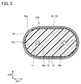
- FIG. FIG. 2 is a cross-sectional view of cable 100. As shown in FIG. FIG. 3 is a partially enlarged view of FIG. 2 in the vicinity of the outer peripheral surface 10a.
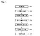
- 4A to 4D are process diagrams showing a method of manufacturing the cable 100.
- FIG. FIG. 5 is a cross-sectional view of the member to be processed 100A prepared in the preparation step S1.
- FIG. 6 is a cross-sectional view of the member 100A to be processed after the intermediate layer forming step S2 is performed.
- FIG. 7 is a cross-sectional view of the member to be processed 100A after the catalyst particle placement step S3 has been performed.
- FIG. 8 is a cross-sectional view of the member to be processed 100A after the oxide layer forming step S4 and the electroless plating step S5 are performed.
- the electroless plated layer may peel off from the outer peripheral surface of the insulating layer. If the electroless plated layer peels off from the outer peripheral surface of the insulating layer due to bending, the transmission characteristics of the cable for differential signal transmission deteriorate at the peeled portion.
- the present disclosure has been made in view of the problems of the prior art as described above. More specifically, the present disclosure provides an actuation signal transmission cable capable of suppressing peeling of the shield layer from the outer peripheral surface of the insulating layer.
- the differential signal transmission cable includes an insulating layer extending along the longitudinal direction of the differential signal transmission cable, and an insulating layer extending along the longitudinal direction. and a shield layer covering the outer peripheral surface of the insulating layer.
- the shield layer has an electroless plated layer containing copper and alloying elements. The types and contents of alloying elements are selected so that tensile stress acts on the shield layer.
- the cable for differential signal transmission of (1) it is possible to suppress peeling of the shield layer from the outer peripheral surface of the insulating layer.
- the copper content in the shield layer may be 90% by mass or more.
- the alloying element may be at least one of nickel, iron and cobalt.
- the nickel content in the shield layer is 0.10 mass percent or more and 3.0 mass percent or less
- the iron content in the shield layer is 0.0010 mass percent or more and 0.0050 mass percent or less
- the content of cobalt in the shield layer may satisfy at least one of 0.0010 mass percent or more and 0.0050 mass percent or less.
- the differential signal transmission cable of (1) or (2) may further include a metal oxide layer between the insulating layer and the shield layer.
- the value obtained by dividing the atomic ratio of iron by the atomic ratio of copper may be 0.000010 or more and 0.00010 or less.
- the value obtained by dividing the atomic ratio of nickel by the atomic ratio of copper may be 0.000050 or more and 0.00080 or less.
- the value obtained by dividing the atomic ratio of cobalt by the atomic ratio of copper may be 0.000010 or more and 0.00010 or less.
- the cables for differential signal transmission of (1) to (3) may further include catalytic particles between the insulating layer and the shield layer.
- the catalyst particles may be particles containing palladium.
- the cables for differential signal transmission of (1) to (4) may further include an intermediate layer covering the outer peripheral surface of the insulating layer.
- the shield layer may cover the outer peripheral surface of the intermediate layer.
- the differential signal transmission cable includes an insulating layer extending along the longitudinal direction of the differential signal transmission cable and an insulating layer extending along the longitudinal direction. , a pair of signal lines embedded inside an insulating layer, and a shield layer covering the outer peripheral surface of the insulating layer.
- the hardness of the insulating layer is 0.020 GPa or more.
- the hardness of the shield layer is 4.0 GPa or less.
- the cable for differential signal transmission of (6) it is possible to suppress peeling of the shield layer from the outer peripheral surface of the insulating layer.
- the value obtained by dividing the hardness of the shield by the hardness of the insulating layer may be 20 or more and 100 or less.
- the insulating layer is a portion at a distance of up to 50 ⁇ m from the outer peripheral surface of each of the pair of signal lines in a cross section orthogonal to the longitudinal direction. It may have a first portion and a second portion whose distance from the outer peripheral surface of the insulating layer is up to 50 ⁇ m. A value obtained by dividing the hardness of the first portion by the hardness of the second portion may be 1.05 or more and 1.50 or less.
- the cable for differential signal transmission of (8) can be made easier to bend.
- a differential signal transmission cable includes an insulating layer extending along the longitudinal direction of the differential signal transmission cable and an insulating layer extending along the longitudinal direction. , a pair of signal lines embedded inside an insulating layer, and a shield layer covering the outer peripheral surface of the insulating layer.
- the shield layer contains copper.
- the crystallite size of copper in the shield layer is 20 nm or more and 75 nm or less.
- the cable for differential signal transmission of (10) it is possible to suppress peeling of the shield layer from the outer peripheral surface of the insulating layer.
- a differential signal transmission cable according to the embodiment is referred to as a cable 100 .
- FIG. 1 is a perspective view of the cable 100.
- FIG. FIG. 2 is a cross-sectional view of cable 100. As shown in FIG. FIG. 2 shows a cross section perpendicular to the longitudinal direction of the cable 100 .
- FIG. 3 is a partially enlarged view of FIG. 2 in the vicinity of the outer peripheral surface 10a.
- the cable 100 includes an insulating layer 10, a signal line 20a, a signal line 20b, an intermediate layer 30, a metal oxide layer 40 and a shield layer 50. and catalyst particles 60 .
- the insulating layer 10 extends along the longitudinal direction of the cable 100.
- the insulating layer 10 is made of an electrically insulating material.
- the insulating layer 10 is made of, for example, polyethylene (PE), tetrafluoroethylene-hexafluoropropylene copolymer (FEP), polypropylene (PP), cyclic olefin polymer, or polymethylpentene. Insulating layer 10 may be a layer containing one or more of these materials.
- the hardness of the insulating layer 10 is preferably 0.020 GPa or more.
- the hardness of the insulating layer 10 may be 0.0035 GPa or more.
- a direction orthogonal to the longitudinal direction of the cable 100 is defined as a first direction DR1 and a second direction DR2.
- the first direction DR1 and the second direction DR2 are orthogonal to each other.
- the insulating layer 10 has, for example, an elliptical shape with a long axis along the first direction DR1.
- the insulating layer 10 has an outer peripheral surface 10a.
- the insulating layer 10 has a first portion 11 and a second portion 12 .
- the first portion 11 is a portion up to 50 ⁇ m from the outer peripheral surface of the signal line 20a (signal line 20b).
- the second portion 12 is a portion whose distance from the outer peripheral surface 10a is up to 50 ⁇ m.
- the hardness of the second portion 12 is preferably smaller than the hardness of the first portion 11 .
- the value obtained by dividing the hardness of the first portion 11 by the hardness of the second portion is preferably 1.05 or more and 1.50 or less.
- the hardness of the insulating layer 10 (first portion 11, second portion 12) is measured using a tripoindenter Hysitron TI980 manufactured by Bruker. In this measurement, a Berkovich indenter is used as an indenter. The maximum load is 8mN. The load time is 5 seconds. The maximum load holding time is 0 seconds. This measurement is performed at 25° C. in air. Note that analysis by the TI980 is performed using TribScan, which is dedicated software for the TI980. Also, this measurement is performed on a sample embedded in an epoxy resin and mirror-polished.
- the signal line 20a and the signal line 20b are paired.
- a signal having a phase opposite to that applied to the signal line 20a is applied to the signal line 20b.
- the cable 100 transmits differential signals.
- the signal lines 20 a and 20 b are embedded inside the insulating layer 10 .
- the signal line 20 a and the signal line 20 b extend along the longitudinal direction of the cable 100 .
- the signal lines 20a and 20b are made of a conductive material.
- the signal line 20a and the signal line 20b are made of copper (Cu), for example. However, the material forming the signal lines 20a and 20b is not limited to copper.
- the signal line 20a and the signal line 20b are arranged, for example, along the first direction DR1.
- the intermediate layer 30 covers the outer peripheral surface 10a.
- the intermediate layer 30 has an outer peripheral surface 30a.
- the intermediate layer 30 is made of an electrically insulating material.
- the intermediate layer 30 is made of polyolefin, for example.
- the intermediate layer 30 may be made of acrylonitrile-butadiene-styrene resin (ABS resin).
- the metal oxide layer 40 is a layer of metal oxide.
- the metal oxide layer 40 mainly contains copper oxide (CuO).
- the metal oxide layer 40 may contain elements other than copper and oxygen.
- the metal oxide layer 40 may further contain, for example, at least one of nickel (Ni), iron (Fe), and cobalt (Co).
- A be the atomic ratio of copper in the metal oxide layer 40 (unit: atomic percent).
- B be the atomic ratio of iron in the metal oxide layer (unit: atomic percent).
- C be the atomic ratio of nickel in the metal oxide layer 40 (unit: atomic percent).
- D be the atomic ratio of cobalt in the metal oxide layer 40 (unit: atomic percent).
- the value obtained by dividing B by A is preferably 0.000010 or more and 0.00010 or less.
- the value obtained by dividing C by A is preferably 0.000050 or more and 0.00080 or less.
- the value obtained by dividing D by A is preferably 0.000010 or more and 0.00010 or less.
- the values of A, B, C and D are measured using EDX (Energy Dispersive X-ray spectroscopy).
- the metal oxide layer 40 covers the outer peripheral surface 30a.
- the metal oxide layer 40 preferably covers the outer peripheral surface 30a over the entire circumference. However, the metal oxide layer 40 may not partially cover the outer peripheral surface 30a. In this case, a portion of the outer peripheral surface 30 a that is not covered with the metal oxide layer 40 is in contact with the shield layer 50 .
- the metal oxide layer 40 has a first surface 40a and a second surface 40b.
- the first surface 40a is a surface facing the intermediate layer 30 side.
- the second surface 40b is the opposite surface of the first surface 40a.
- the second surface 40b faces the shield layer 50 side.
- the metal oxide layer 40 contacts the intermediate layer 30 on the first surface 40a and contacts the shield layer 50 on the second surface 40b.
- the shield layer 50 covers the second surface 40b. That is, the shield layer 50 covers the outer peripheral surface 10a with the intermediate layer 30 and the metal oxide layer 40 interposed therebetween.
- the shield layer 50 has conductivity.
- the shield layer 50 has, for example, an electroless plated layer 51 and an electrolytic plated layer 52 .
- the electroless plated layer 51 covers the metal oxide layer 40 .
- the electroplated layer 52 covers the electroless plated layer 51 .
- the electroless plating layer 51 is a layer formed by electroless plating. Electroless plated layer 51 contains copper. The electroless plated layer 51 further contains alloying elements. The types and contents of alloying elements are selected to induce tensile stress in the shield layer 50 .
- An alloying element is, for example, an element that forms a solid solution with copper. More specifically, the alloying element is at least one of iron, nickel and cobalt. However, alloying elements are not limited to iron, nickel and cobalt.
- the electrolytic plated layer 52 is a layer formed by electrolytic plating. Electroplated layer 52 contains, for example, copper.
- the electroless plated layer 51 contains the above alloy elements, the above alloy elements form a solid solution in the copper in the electroless plated layer 51, and the copper crystals in the electroless plated layer 51 are distorted. will occur.
- the electroplating layer 52 is also strained when the electroless plating layer 51 contains the above alloy elements. occurs. Due to such strain, tensile stress remains in the shield layer 50 .
- the copper content in the shield layer 50 is, for example, 90% by mass or more.
- the content of iron in the shield layer 50 is preferably 0.0010% by mass or more and 0.0050% by mass or less.
- the nickel content in the shield layer 50 is preferably 0.10 mass percent or more and 3.0 mass percent or less.
- the content of cobalt in the shield layer 50 is preferably 0.0010% by mass or more and 0.0050% by mass or less.
- the nickel content in the shield layer 50 is 0.10 mass percent or more and 3.0 mass percent or less
- the iron content in the shield layer 50 is 0.0010 mass percent or more and 0.0050 mass percent.
- that the cobalt content in the shield layer 50 is 0.0010% by mass or more and 0.0050% by mass or less.
- the contents of copper, iron, nickel and cobalt in the shield layer 50 are measured by dissolving the shield layer 50 in a solution and subjecting the solution to ICP (Inductive Coupled Plasma) emission spectrometry.
- ICP Inductive Couple
- the hardness of the shield layer 50 is preferably 4.0 GPa or less.
- the value obtained by dividing the hardness of shield layer 50 by the hardness of insulating layer 10 is preferably 20 or more and 100 or less.
- the hardness of the shield layer 50 is measured using a tripoindenter Hysitron TI980 manufactured by Bruker. In this measurement, a Berkovich indenter is used as an indenter. The maximum load is 30 ⁇ N. The load time is 2 seconds. The maximum load holding time is 2 seconds. This measurement is performed at 25° C. in air. Note that analysis by the TI980 is performed using TribScan, which is dedicated software for the TI980. Also, this measurement is performed on a sample embedded in an epoxy resin and mirror-polished.
- the crystallite size of copper in the shield layer 50 is preferably 20 nm or more and 75 nm or less.
- the crystallite size of copper in the shield layer 50 is more preferably 20 nm to 60 nm or less.
- the shield layer 50 contains copper crystal grains. A portion of a crystal grain that can be regarded as a single crystal is called a crystallite. Therefore, the crystallite size of copper in the shield layer 50 is equal to or smaller than the grain size of the copper crystal grains contained in the shield layer 50 .
- the crystallite size of copper in the shield layer 50 can be measured using an X-ray diffraction method. More specifically, X-ray diffraction is performed using Rigaku SmartLab. In this measurement, the X-ray source is CuK ⁇ , the incident light source is CBO-f, and the detector is Hypix-3000. The X-ray diffraction is performed in the range of the diffraction angle 2 ⁇ from 20° to 80°, and the step of changing the diffraction angle 2 ⁇ is 0.03°.
- the line profile obtained by X-ray diffraction of the sample has a shape that includes both the true spread due to the physical quantity of the crystallite size of the sample and the spread due to the measurement device.
- the component due to the apparatus is removed from the line profile obtained by X-ray diffraction for the sample, and the true line profile integral width (peak integrated intensity divided by peak height value). Substituting the integrated width of the true line profile into the Scherrer equation gives the crystallite size of the sample.
- LaB 6 manufactured by NIST is used as a standard sample for removing components caused by the apparatus from the line profile obtained by X-ray diffraction of the sample.
- ⁇ be the integral width of the true line profile
- ⁇ 1 be the integral width of the line profile obtained by X-ray diffraction for the sample
- ⁇ 2 be the integral width of the line profile obtained by X-ray diffraction for the standard sample.
- D is the crystallite size of the sample
- ⁇ is the X-ray wavelength
- ⁇ is the Bragg angle of the Cu200 diffraction line.
- the catalyst particles 60 are between the insulating layer 10 and the shield layer 50. More specifically, shield layer 50 is in metal oxide layer 40 . Catalyst particles 60 are also present at the interface between metal oxide layer 40 and intermediate layer 30 .
- the catalyst particles 60 are, for example, particles containing palladium (Pd).
- FIG. 4A to 4D are process diagrams showing a method of manufacturing the cable 100.
- the method for manufacturing the cable 100 includes a preparation step S1, an intermediate layer forming step S2, a catalyst particle placement step S3, an oxide layer forming step S4, an electroless plating step S5, an electrolysis It has a plating step S6 and a heat treatment step S7.
- the intermediate layer forming step S2 is performed.
- the catalyst particle arranging step S3 is performed.
- the oxide layer forming step S4 is performed after the catalyst particle arranging step S3.
- Electroless plating process S5 is performed after oxide layer formation process S4.
- an electrolytic plating step S6 is performed.
- a heat treatment step S7 is performed after the electroplating step S6.
- FIG. 5 is a cross-sectional view of the member to be processed 100A prepared in the preparation step S1.
- the processing target member 100A has an insulating layer 10, signal lines 20a, and signal lines 20b.
- FIG. 6 is a cross-sectional view of the member to be processed 100A after the intermediate layer forming step S2 has been performed.
- intermediate layer forming step S2 intermediate layer 30 is formed to cover outer peripheral surface 10a.
- the material forming the intermediate layer 30 is applied to the outer peripheral surface 10a, and the applied material is cured to form the intermediate layer 30 so as to cover the outer peripheral surface 10a.
- FIG. 7 is a cross-sectional view of the member to be processed 100A after the catalyst particle placement step S3 has been performed.
- catalyst particles 60 are dispersed and placed on the outer peripheral surface 30a.
- a solution containing the catalyst particles 60 is applied to the outer peripheral surface 30a, and the solution is volatilized to disperse and arrange the catalyst particles 60 on the outer peripheral surface 30a.
- FIG. 8 is a cross-sectional view of the member 100A to be processed after the oxide layer forming step S4 and the electroless plating step S5 have been performed. As shown in FIG. 8, the metal oxide layer 40 is formed in the oxide layer forming step S4, and the electroless plated layer 51 is formed on the metal oxide layer 40 in the electroless plating step S5.
- the material contained in the electroless plating layer 51 is dissolved, and the member 100A to be processed is placed in a plating solution bubbled with an oxygen-containing gas (for example, air). is immersed.
- an oxygen-containing gas for example, air
- the metal oxide layer 40 is formed so as to cover the outer peripheral surface 30a with the catalyst particles 60 as nuclei.
- the catalyst particles 60 the cores of the growth of the metal oxide layer 40 are present in the metal oxide layer 40, and the others are present at the interface between the intermediate layer 30 and the metal oxide layer 40. .
- alloy elements such as iron, nickel, and cobalt
- electroless plating layer 51 is plated on metal oxide layer 40 .
- an electrolytic plating layer 52 is formed so as to cover the electroless plating layer 51.
- the member to be processed 100A is immersed in a plating solution in which the material contained in the electrolytic plating layer 52 is dissolved, and the electroless plating layer 51 is energized. Electrolytic plating layer 52 is thereby plated on electroless plating layer 51, and cable 100 having the structure shown in FIGS. 1 to 3 is manufactured.
- the cable 100 is heat treated.
- This heat treatment causes the crystal grains of copper contained in the shield layer 50 to grow, and accordingly the crystallite size in the shield layer 50 also increases. Since the hardness of the shield layer 50 decreases as the grain size of the copper crystal grains contained in the shield layer 50 increases (Hall-Petch rule), this heat treatment decreases the hardness of the shield layer 50. . Further, the heat treatment promotes crystallization of the resin material forming the insulating layer 10, so that the hardness of the insulating layer 10 increases with the heat treatment.
- the cable 100 may be used in a bent state.
- a compressive bending stress acts on the shield layer 50 inside the cable 100 in a bent state. This compressive bending stress may cause the shield layer 50 to buckle and separate from the insulating layer 10 inside the cable 100 in the bent state. When such peeling occurs, the transmission characteristics of the cable 100 deteriorate.
- the cable 100 tensile stress acts on the shield layer 50 because the electroless plated layer 51 contains an alloying element.
- the compressive stress applied to the shield layer 50 inside the cable 100 in a bent state is alleviated, and the peeling caused by the buckling of the shield layer 50 is suppressed. It is possible to suppress the deterioration of the transmission characteristics of the cable 100.
- the plating solution used to form the electroless plating layer 51 is chemically unstable and difficult to handle. As described above, when the electroless plating layer 51 contains at least one of iron and nickel, these elements are added to the plating solution used to form the electroless plating layer 51 . The addition of iron, nickel and cobalt chemically stabilizes the plating solution used to form the electroless plating layer 51 . Therefore, when the electroless plated layer 51 contains at least one of iron, nickel and cobalt, it is possible to stabilize the manufacturing process of the cable 100 .
- the cable 100 has a metal oxide layer 40 , and hydrogen bonding occurs between the shield layer 50 (the electroless plated layer 51 ) and the metal oxide layer 40 .
- hydrogen bonding occurs between the shield layer 50 (the electroless plated layer 51 ) and the metal oxide layer 40 .
- adhesion between the insulating layer 10 and the shield layer 50 is ensured without roughening the outer peripheral surface 10a.
- the cable 100 has the metal oxide layer 40, it is possible to ensure the adhesion of the shield layer 50 to the insulating layer 10 while ensuring transmission characteristics in the high frequency range of the cable 100. is.
- the insulating layer 10 inside the cable 100 in the bent state will be recessed toward the inside of the cable 100 .
- the shield layer 50 inside the cable 100 in the bent state is bent toward the inside of the cable 100 .
- wrinkles occur inside the cable 100 when the cable 100 is bent, degrading the transmission characteristics.
- the hardness of the insulating layer 10 is 0.020 GPa or more and the hardness of the shield layer 50 is 4.0 GPa or less. becomes smaller, and it is possible to suppress the deterioration of the transmission characteristics when the cable 100 is bent.
- the value obtained by dividing the hardness of the shield layer 50 by the hardness of the insulating layer 10 is 20 or more and 100 or less, it is possible to further suppress deterioration of transmission characteristics when the cable 100 is bent.
- the crystallite size of copper in the shield layer 50 is 20 nm or more and 75 nm or less, the hardness of the shield layer 50 can be reduced, so that deterioration of transmission characteristics when the cable 100 is similarly bent can be further suppressed. is possible.
- the geometrical moment of inertia of the insulating layer 10 becomes small, and the deformation of the cable 100 The deformation of the insulating layer 10 can easily follow. Therefore, in this case, when the cable 100 is bent, the insulating layer 10 is less likely to peel off from the signal wire 20a (signal wire 20b).
- First loss evaluation test In the first loss evaluation test, the relationship between the content of alloy elements in the shield layer 50 (the electroless plated layer 51) and the transmission characteristics of the cable 100 was evaluated. Samples 1-1 to 1-9 were used as samples of the cable 100 for the first loss evaluation test. As shown in Table 1, the contents of nickel, iron and cobalt in the shield layer 50 were changed in samples 1-1 to 1-9. Although not shown in Table 1, in Samples 1-1 to 1-9, the copper content in the shield layer 50 was set to 90% by mass or more.
- the transmission characteristics were evaluated by measuring the insertion loss in the differential mode of each sample while winding each sample around a cylinder with a diameter of 50 mm. If there is no difference in the insertion loss in the differential mode before and after this winding, or if the insertion loss in the differential mode after this winding is -25 dB / m or more, it is evaluated as OK, and after this winding A case where the insertion loss in the differential mode was less than -25 dB/m was evaluated as NG.
- Condition 1 is that the nickel content in the shield layer 50 is 0.10 mass percent or more and 3.0 mass percent or less, and the iron content in the shield layer 50 is 0.0010 mass percent or more and 0.0050 mass percent. % or less, and condition 3 is that the cobalt content in the shield layer 50 is 0.0010% by mass or more and 0.0050% by mass or less.
- Samples 2-1 to 2-3 were used as samples of the cable 100 for the second loss evaluation test. As shown in Table 2, in samples 2-1 to 2-3, the atomic ratios of copper, nickel, iron and cobalt in the shield layer 50 were changed. Accordingly, in samples 2-1 to 2-3, the value obtained by dividing B by A, the value obtained by dividing C by A, and the value obtained by dividing D by A were changed.
- Condition 4 is that the value obtained by dividing B by A is 0.000010 or more and 0.00010 or less
- Condition 5 is that the value obtained by dividing C by A is 0.000010 or more and 0.00080 or less
- D is Condition 6 is that the value obtained by dividing by A is 0.000010 or more and 0.00010.
- the transmission characteristics of each sample were evaluated by the same method as in the first loss evaluation test.
- samples 3-1 to 3-10 the value obtained by dividing the hardness of the shield layer 50 by the hardness of the insulating layer 10 was in the range of 20 or more and 100 or less.
- sample 3-11 the value obtained by dividing the hardness of the shield layer 50 by the hardness of the insulating layer 10 was not within the range of 20 or more and 100 or less.
- Samples 3-1 to 3-10 were all evaluated as OK in terms of transmission characteristics.
- Sample 3-11 was evaluated as NG in terms of transmission characteristics.
- the transmission characteristics of each sample were evaluated using the same method as in the first loss evaluation test.
- samples 4-1 and 4-2 the value obtained by dividing the hardness of the first portion 11 by the hardness of the second portion 12 was within the range of 1.05 or more and 1.50 or less.
- sample 4-3 the value obtained by dividing the hardness of the first portion 11 by the hardness of the second portion 12 was not within the range of 1.05 to 1.50.
- Samples 4-1 and 4-2 were both evaluated as OK in terms of transmission characteristics.
- Sample 4-3 was evaluated as NG in terms of transmission characteristics.
- the transmission characteristics of each sample were evaluated using the same method as in the first loss evaluation test.
- the crystallite size in the shield layer 50 was within the range of 20 nm or more and 75 nm or less.
- the crystallite size in the shield layer 50 was not within the range of 20 nm or more and 75 nm or less.
- samples 5-1 to 5-3 the crystallite size in the shield layer 50 was within the range of 20 nm or more and 60 nm or less.
- sample 5-4 the crystallite size in the shield layer 50 was not within the range of 20 nm or more and 60 nm or less.
- the transmission characteristics of samples 5-1 to 5-3 were superior to the transmission characteristics of sample 5-4. From this comparison, it was experimentally clarified that deterioration of transmission characteristics due to bending of the cable 100 can be further suppressed by setting the crystallite size in the shield layer 50 to 20 nm or more and 60 nm or less.
Landscapes
- Engineering & Computer Science (AREA)
- Manufacturing & Machinery (AREA)
- Microelectronics & Electronic Packaging (AREA)
- Insulated Conductors (AREA)
Priority Applications (5)
| Application Number | Priority Date | Filing Date | Title |
|---|---|---|---|
| US18/286,019 US20240196582A1 (en) | 2021-07-01 | 2021-07-01 | Differential signal transmission cable |
| JP2023531287A JP7750289B2 (ja) | 2021-07-01 | 2021-07-01 | 差動信号伝送用ケーブル |
| DE112021007918.2T DE112021007918T5 (de) | 2021-07-01 | 2021-07-01 | Differentialsignalübertragungskabel |
| CN202180096922.5A CN117157719A (zh) | 2021-07-01 | 2021-07-01 | 差动信号传输用电缆 |
| PCT/JP2021/024930 WO2023276104A1 (ja) | 2021-07-01 | 2021-07-01 | 差動信号伝送用ケーブル |
Applications Claiming Priority (1)
| Application Number | Priority Date | Filing Date | Title |
|---|---|---|---|
| PCT/JP2021/024930 WO2023276104A1 (ja) | 2021-07-01 | 2021-07-01 | 差動信号伝送用ケーブル |
Publications (1)
| Publication Number | Publication Date |
|---|---|
| WO2023276104A1 true WO2023276104A1 (ja) | 2023-01-05 |
Family
ID=84691681
Family Applications (1)
| Application Number | Title | Priority Date | Filing Date |
|---|---|---|---|
| PCT/JP2021/024930 Ceased WO2023276104A1 (ja) | 2021-07-01 | 2021-07-01 | 差動信号伝送用ケーブル |
Country Status (5)
| Country | Link |
|---|---|
| US (1) | US20240196582A1 (https=) |
| JP (1) | JP7750289B2 (https=) |
| CN (1) | CN117157719A (https=) |
| DE (1) | DE112021007918T5 (https=) |
| WO (1) | WO2023276104A1 (https=) |
Citations (4)
| Publication number | Priority date | Publication date | Assignee | Title |
|---|---|---|---|---|
| JP2004172045A (ja) * | 2002-11-22 | 2004-06-17 | Totoku Electric Co Ltd | 細径セミリジッド同軸ケーブルの製造方法 |
| JP2007146247A (ja) * | 2005-11-29 | 2007-06-14 | Hitachi Cable Ltd | 金属と樹脂からなる複合材料及びその製造方法並びにそれを用いた製品 |
| JP2008004275A (ja) * | 2006-06-20 | 2008-01-10 | Nissei Electric Co Ltd | 2芯平行同軸ケーブル |
| JP2019175678A (ja) * | 2018-03-28 | 2019-10-10 | 日立金属株式会社 | 差動信号伝送用ケーブル、多芯ケーブル、及び差動信号伝送用ケーブルの製造方法 |
Family Cites Families (6)
| Publication number | Priority date | Publication date | Assignee | Title |
|---|---|---|---|---|
| ES2704258T3 (es) * | 2014-04-25 | 2019-03-15 | Paramount Int Services Ltd | Sistema de impresión de huecograbado o rotograbado y preparación y uso del mismo |
| CN204303452U (zh) | 2014-12-03 | 2015-04-29 | 东莞讯滔电子有限公司 | 线缆 |
| JP6245402B1 (ja) | 2017-07-04 | 2017-12-13 | 日立金属株式会社 | 差動信号伝送用ケーブル、多芯ケーブル、及び差動信号伝送用ケーブルの製造方法 |
| JP2019169579A (ja) | 2018-03-23 | 2019-10-03 | 株式会社東芝 | 半導体装置及びその製造方法 |
| WO2021075421A1 (ja) * | 2019-10-18 | 2021-04-22 | 富士フイルム株式会社 | タッチセンサー部材前駆体およびタッチセンサー部材の製造方法 |
| CN116783664A (zh) * | 2021-02-18 | 2023-09-19 | 住友电气工业株式会社 | 差动信号传输用电缆 |
-
2021
- 2021-07-01 US US18/286,019 patent/US20240196582A1/en active Pending
- 2021-07-01 WO PCT/JP2021/024930 patent/WO2023276104A1/ja not_active Ceased
- 2021-07-01 JP JP2023531287A patent/JP7750289B2/ja active Active
- 2021-07-01 DE DE112021007918.2T patent/DE112021007918T5/de active Pending
- 2021-07-01 CN CN202180096922.5A patent/CN117157719A/zh active Pending
Patent Citations (4)
| Publication number | Priority date | Publication date | Assignee | Title |
|---|---|---|---|---|
| JP2004172045A (ja) * | 2002-11-22 | 2004-06-17 | Totoku Electric Co Ltd | 細径セミリジッド同軸ケーブルの製造方法 |
| JP2007146247A (ja) * | 2005-11-29 | 2007-06-14 | Hitachi Cable Ltd | 金属と樹脂からなる複合材料及びその製造方法並びにそれを用いた製品 |
| JP2008004275A (ja) * | 2006-06-20 | 2008-01-10 | Nissei Electric Co Ltd | 2芯平行同軸ケーブル |
| JP2019175678A (ja) * | 2018-03-28 | 2019-10-10 | 日立金属株式会社 | 差動信号伝送用ケーブル、多芯ケーブル、及び差動信号伝送用ケーブルの製造方法 |
Also Published As
| Publication number | Publication date |
|---|---|
| CN117157719A (zh) | 2023-12-01 |
| DE112021007918T5 (de) | 2024-05-16 |
| JP7750289B2 (ja) | 2025-10-07 |
| JPWO2023276104A1 (https=) | 2023-01-05 |
| US20240196582A1 (en) | 2024-06-13 |
Similar Documents
| Publication | Publication Date | Title |
|---|---|---|
| JP5705311B2 (ja) | 銅箔複合体及びそれに使用される銅箔、並びに成形体及びその製造方法 | |
| KR101363183B1 (ko) | 전자파 실드용 복합체 | |
| US20200332428A1 (en) | Method for manufacturing copper foil for high frequency circuit | |
| KR102170014B1 (ko) | 표면 처리 구리박, 부극 집전체 및 비수계 이차 전지의 부극재 | |
| WO2017212770A1 (ja) | 斜め巻きばね用線材、斜め巻きばねおよびそれらの製造方法 | |
| EP2402485A1 (en) | Metal-coated polyimide resin substrate with excellent thermal aging resistance properties | |
| KR20160117196A (ko) | 플렉시블 프린트 기판용 구리 합금박, 그것을 사용한 구리 피복 적층체, 플렉시블 프린트 기판 및 전자 기기 | |
| JP5356714B2 (ja) | エッチング性に優れたフレキシブルプリント基板用銅合金箔及びそれを用いたフレキシブルプリント基板 | |
| CN110277192B (zh) | 镀锡铜线及其制造方法以及绝缘电线、电缆 | |
| WO2020137726A1 (ja) | 銅合金板、めっき皮膜付銅合金板及びこれらの製造方法 | |
| WO2023276104A1 (ja) | 差動信号伝送用ケーブル | |
| CN113811958B (zh) | 铜包钢线、绞合线、绝缘电线及线缆 | |
| CN107109546A (zh) | 铝合金电线以及使用该铝合金电线的线束 | |
| CN115298334B (zh) | Cu-Ni-Si系铜合金板、带镀膜的Cu-Ni-Si系铜合金板及它们的制造方法 | |
| CN114981902B (zh) | 差动信号传送用线缆 | |
| JP5467789B2 (ja) | 伸線加工性の良好なAlめっき鋼線およびその製造方法 | |
| JP2006307277A (ja) | 極細めっき線の製造方法 | |
| CN112585699A (zh) | 包覆电线、带端子电线、铜合金线、铜合金绞合线以及铜合金线的制造方法 | |
| US20150140357A1 (en) | Layer For An Electrical Contact Element, Layer System And Method For Producing A Layer | |
| CN1397657A (zh) | 层叠板用铜合金箔 | |
| JP4686931B2 (ja) | 超極細同軸ケーブル | |
| JP7677397B2 (ja) | 差動信号伝送用ケーブル | |
| JP4412137B2 (ja) | 同軸ケーブルの製造方法並びにその同軸ケーブルを用いた接続ケーブル | |
| CN114901873A (zh) | 电解铜箔 | |
| JP6746445B2 (ja) | 同軸ケーブル |
Legal Events
| Date | Code | Title | Description |
|---|---|---|---|
| 121 | Ep: the epo has been informed by wipo that ep was designated in this application |
Ref document number: 21948408 Country of ref document: EP Kind code of ref document: A1 |
|
| ENP | Entry into the national phase |
Ref document number: 2023531287 Country of ref document: JP Kind code of ref document: A |
|
| WWE | Wipo information: entry into national phase |
Ref document number: 18286019 Country of ref document: US |
|
| NENP | Non-entry into the national phase |
Ref country code: DE |
|
| 122 | Ep: pct application non-entry in european phase |
Ref document number: 21948408 Country of ref document: EP Kind code of ref document: A1 |