WO2023276002A1 - プローブ装置 - Google Patents
プローブ装置 Download PDFInfo
- Publication number
- WO2023276002A1 WO2023276002A1 PCT/JP2021/024581 JP2021024581W WO2023276002A1 WO 2023276002 A1 WO2023276002 A1 WO 2023276002A1 JP 2021024581 W JP2021024581 W JP 2021024581W WO 2023276002 A1 WO2023276002 A1 WO 2023276002A1
- Authority
- WO
- WIPO (PCT)
- Prior art keywords
- camera
- probe
- optical axis
- sample
- stage
- Prior art date
- Legal status (The legal status is an assumption and is not a legal conclusion. Google has not performed a legal analysis and makes no representation as to the accuracy of the status listed.)
- Ceased
Links
Images





Classifications
-
- G—PHYSICS
- G01—MEASURING; TESTING
- G01R—MEASURING ELECTRIC VARIABLES; MEASURING MAGNETIC VARIABLES
- G01R1/00—Details of instruments or arrangements of the types included in groups G01R5/00 - G01R13/00 and G01R31/00
- G01R1/02—General constructional details
- G01R1/04—Housings; Supporting members; Arrangements of terminals
- G01R1/0408—Test fixtures or contact fields; Connectors or connecting adaptors; Test clips; Test sockets
-
- G—PHYSICS
- G01—MEASURING; TESTING
- G01R—MEASURING ELECTRIC VARIABLES; MEASURING MAGNETIC VARIABLES
- G01R1/00—Details of instruments or arrangements of the types included in groups G01R5/00 - G01R13/00 and G01R31/00
- G01R1/02—General constructional details
- G01R1/06—Measuring leads; Measuring probes
- G01R1/067—Measuring probes
- G01R1/06794—Devices for sensing when probes are in contact, or in position to contact, with measured object
-
- G—PHYSICS
- G06—COMPUTING OR CALCULATING; COUNTING
- G06T—IMAGE DATA PROCESSING OR GENERATION, IN GENERAL
- G06T7/00—Image analysis
- G06T7/70—Determining position or orientation of objects or cameras
- G06T7/73—Determining position or orientation of objects or cameras using feature-based methods
- G06T7/74—Determining position or orientation of objects or cameras using feature-based methods involving reference images or patches
-
- H—ELECTRICITY
- H10—SEMICONDUCTOR DEVICES; ELECTRIC SOLID-STATE DEVICES NOT OTHERWISE PROVIDED FOR
- H10P—GENERIC PROCESSES OR APPARATUS FOR THE MANUFACTURE OR TREATMENT OF DEVICES COVERED BY CLASS H10
- H10P74/00—Testing or measuring during manufacture or treatment of wafers, substrates or devices
-
- G—PHYSICS
- G06—COMPUTING OR CALCULATING; COUNTING
- G06T—IMAGE DATA PROCESSING OR GENERATION, IN GENERAL
- G06T2207/00—Indexing scheme for image analysis or image enhancement
- G06T2207/10—Image acquisition modality
- G06T2207/10056—Microscopic image
- G06T2207/10061—Microscopic image from scanning electron microscope
-
- G—PHYSICS
- G06—COMPUTING OR CALCULATING; COUNTING
- G06T—IMAGE DATA PROCESSING OR GENERATION, IN GENERAL
- G06T2207/00—Indexing scheme for image analysis or image enhancement
- G06T2207/30—Subject of image; Context of image processing
- G06T2207/30108—Industrial image inspection
- G06T2207/30148—Semiconductor; IC; Wafer
-
- G—PHYSICS
- G06—COMPUTING OR CALCULATING; COUNTING
- G06T—IMAGE DATA PROCESSING OR GENERATION, IN GENERAL
- G06T2207/00—Indexing scheme for image analysis or image enhancement
- G06T2207/30—Subject of image; Context of image processing
- G06T2207/30204—Marker
Definitions
- the present invention relates to a probe device that measures sample properties by bringing a mechanical probe into contact with the sample surface.
- a probe device defect inspection device
- probes semiconductor devices
- SEM scanning electron microscope
- the SEM has high spatial resolution, it is not suitable for imaging a wide range at low magnification and has a shallow depth of focus.
- Patent Document 1 in order to quickly position the probe, before the stylus of the probe by SEM, the probe and the sample are approached by rough adjustment (rough alignment) using an optical image. is provided in parallel with an electron optical system device.
- the probe rough-approach image acquisition device is fixed to the sample chamber.
- the positional relationship between the sample surface and the optical axis of the side observation camera differs for each sample, so the appearance of the sample surface and the tip of the probe in the optical image differs.
- the height of the sample stage on which the sample is placed is changed according to the working distance.
- the positional relationship of the optical axis of the side observation camera changes, and the appearance of the sample surface and the tip of the probe in the optical image changes.
- the impact may damage the probe. It is unavoidable that there are limits to begin with. However, if there is a difference in appearance in the optical image as described above, it is impossible to accurately measure the separation distance between the sample and the probe, and the probe cannot approach the sample to the limit. If the accuracy of rough alignment is low, the time required for fine adjustment of the probe position using the SEM image will increase. This reduces the throughput of inspection, and may increase the amount of contamination and damage caused by continuing to irradiate the sample with the electron beam for a longer period of time.
- An object of the present invention is to provide a probe device that allows the probe to approach the sample quickly and safely.
- a probe apparatus which is an embodiment of the present invention, comprises a sample stage that supports a sample, a probe unit attached with a probe that contacts a predetermined sample surface of the sample, a first camera that images the sample and the probe, a first camera optical axis adjustment stage for adjusting the optical axis of the first camera, the optical axis of the first camera being parallel to the sample surface; , the optical axis of the camera can be moved in the direction perpendicular to the sample surface.
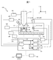
- FIG. 1 is a schematic diagram of a defect inspection device;
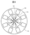
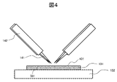
- FIG. FIG. 4 is a front view showing the configuration around the sample and probe; 4 is a plan view showing the configuration of the probe;
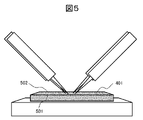
- FIG. It is an optical image when the height of the optical axis of the side observation camera matches the sample surface. It is an optical image when the optical axis of the side observation camera is located at a position higher than the sample surface. It is an optical image when the optical axis of the side observation camera is located at a position lower than the sample surface.
- FIG. 4 is a flow chart illustrating an example of a probe stylus process;
- FIG. It is an example of a SEM image (schematic diagram).
- 5 is a flow chart showing an example of a rough adjustment process using an optical image;
- FIG. 5 is a side view showing a camera position alignment method in a coarse adjustment process using an optical image
- FIG. 11 is a flowchart illustrating an example of a multiple probe proximity process
- FIG. It is an optical image captured by the side observation camera 111A.
- It is a side view which shows the positional relationship of each probe in FIG.11 S1103.
- 7 is a flow chart showing an example of a probe positional relationship acquisition process using a top observation camera. It is an optical image captured by the top observation camera 111B.
- FIG. 4 is a front view showing the positional relationship between probes and markers;
- FIG. 4 is a front view showing the positional relationship between probes and markers;
- FIG. 4 is a front view showing the positional relationship between probes and markers;
- FIG. 4 is a front view showing the positional relationship between probes;
- FIG. 1 is a schematic diagram of a defect inspection device, which is an example of a probe device.
- the defect inspection apparatus 100 mainly includes an electron beam column 101, an electron beam column controller 102, a charged particle detector 103, a charged particle detector controller 104, a camera 111, a camera optical axis adjustment stage 112, and a camera optical axis.
- Adjustment stage controller 113 sample chamber 121, base stage 122, base stage guide 123, base stage controller 124, sample stage 125, sample stage controller 126, probe 141, probe unit 143, probe unit controller 144, control computer 151 , an input device 152 and a display 153 .
- the electron beam column 101 incorporates an electron optical system including an electron source for generating an electron beam, a lens for converging the electron beam, a polarizer for scanning the electron beam, and the like.
- the electron beam column controller 102 is responsible for overall control required to drive the electron beam column 101 .
- An ion beam or the like may be used in place of the electron beam.
- a charged particle beam column having a built-in charged particle optical system corresponding to the charged particle beam used for observation is provided.
- the charged particle detector 103 detects charged particles emitted from the sample 131 by irradiating the sample 131 with an electron beam generated by the electron beam column 101 .
- the charged particle detector 103 is, for example, a secondary electron detector, a backscattered electron detector, a STEM detector, a low energy loss electron detector or an EDX detector.
- a plurality of charged particle detectors 103 may be provided.
- the charged particle detector controller 104 performs arithmetic processing on the signal detected by the charged particle detector 103 and forms an image.
- a decompression device such as a rotary pump, a turbomolecular pump, an ion pump, or a cryopump is connected to the sample chamber 121 in which the sample 131 to be inspected is placed.
- a sample replacement chamber or a probe replacement chamber may be connected.
- a camera 111 is attached to the sample chamber 121 in order to roughly bring the probe 141 to the sample 131 .
- the camera 111 is an imaging device such as an optical microscope, CCD camera, or CMOS camera.
- FIG. 1 shows a state in which the sample 131 is positioned in the SEM observation area directly below the electron beam column 101 in the sample chamber 121 . can be moved to the probe adjustment area inside. In the probe adjustment area, the camera 111 performs imaging for grasping the positional relationship between the sample 131 and the probe 141 .
- the camera 111 is mounted on a camera optical axis adjustment stage 112 whose optical axis is adjustable, and the camera optical axis adjustment stage 112 is driven by a camera optical axis adjustment stage controller 113 .
- the defect inspection device 100 includes a side observation camera 111A and a top observation camera 111B.
- the side observation camera optical axis adjustment stage 112A is a camera optical axis adjustment stage that enables adjustment of the optical axis of the side observation camera 111A.
- the optical axis of the side observation camera 111A is parallel to the horizontal plane (XY plane), and at least vertical movement (movement in the Z direction) is possible.
- the optical axis of the side observation camera 111A extends in the Y direction.
- the top observation camera optical axis adjustment stage 112B is a camera optical axis adjustment stage that enables adjustment of the optical axis of the top observation camera 111B.
- the optical axis of the top observation camera 111B extends in the vertical direction (Z direction) and can be moved horizontally.
- FIG. 1 shows an example in which two cameras 111 are provided so that the positional relationship between the sample 131 and the probe 141 can be grasped from two directions, but it is also possible to use only the side observation camera 111A. In this case, the top observation camera 111B and the top observation camera optical axis adjustment stage 112B may be omitted.
- the base stage 122 is driven by a base stage controller 124 and is horizontally movable along a base stage guide 123 .
- the base stage 122 is moved to the probe adjustment area of the sample chamber 121 and the probe 141 is brought as close to the sample 131 as possible based on the optical image captured by the camera 111 .
- the base stage 122 is moved to the SEM observation area, and the probe 141 is brought into contact with the sample 131 based on the electron microscope image.
- FIG. 2 is a front view showing the configuration around the sample 131 and the probe 141
- FIG. 3 is a plan view showing the configuration of the probe.
- a sample stage 125 and a probe unit 143 are mounted on the base stage 122 .
- the base stage 122, the sample stage 125 and the probe unit 143 each have a drive mechanism such as a stepping motor or piezomotor capable of minute displacement control. That is, the sample stage 125 on the base stage 122 and the probe unit 143 operate with independent drive systems.
- the sample stage 125 is driven by a sample stage controller 126 and is capable of at least horizontal movement and vertical movement.
- a sample holder receiver 127 is mounted on the sample stage 125 .
- the sample holder receiver 127 supports a sample holder 132 on which a sample 131 is placed.
- an insulating material may be arranged between the sample stage 125 and the sample holder receiver 127 in order to ensure the insulating properties of the sample 131 in evaluating the electrical characteristics.
- the sample 131 is supported by the sample stage 125 so that the sample surface with which the probe 141 contacts is parallel to the horizontal plane (XY plane).
- the probe 141 is attached to the probe unit 143 via the probe holder 142 . As shown in FIG. 3, one probe unit 143 is provided for one probe 141 .
- the probe unit 143 is supported by a probe unit support base 145 .
- Probe unit 143 is driven by probe unit controller 144 and is capable of at least horizontal and vertical movement.
- the probe unit controller 144 drives the probe unit 143 to bring the probe 141 into contact with the desired position of the sample 131, and extracts the electrical signal detected by the probe 141. Based on the obtained electrical signal, the electrical properties of the sample 131 can be measured by an electrical property measuring device such as a semiconductor parameter analyzer.
- the control computer 151 (FIG. 1) controls the operation of the defect inspection apparatus 100 as a whole.
- An input device 152 and a display 153 are connected to the control computer 151 .
- the input device 152 is a device for the user to input various instructions to the defect inspection apparatus 100, and can use, for example, a keyboard or mouse.
- the instructions include, for example, instructions to change the irradiation conditions of the electron beam by the electron beam column 101 and to move the base stage 122, the sample stage 125 and the probe unit 143.
- the display 153 displays the user interface and the like output by the control computer 151 .
- the user interface is a screen for displaying the control state of the defect inspection apparatus 100 and for changing the control state by the user inputting an instruction using the input device 152 .
- One display 153 or a plurality of displays 153 may be provided, and the display 153 may have the function of the input device 152 like a touch panel.
- the control computer 151 includes an electron beam column control section 161 , a detector signal processing section 162 , a camera image processing section 163 , a camera optical axis adjustment stage control section 164 and a stage control section 165 .
- the roles of these control units and processing units will be described later, but the control conditions for these control units are set by the user through the user interface screen, and the images and information generated by these processing units are transmitted to the user through the user interface screen. Is displayed.
- the control computer 151 controls the electron beam column controller 102 , the charged particle detector controller 104 , the camera 111 , the camera optical axis adjustment stage controller 113 , the base stage controller 124 , the sample stage controller 126 and the probe unit controller 144 . Mutual communication is possible with each.
- Each controller of the control computer 151 controls the operation of each controller to execute the inspection.
- the control computer 151 may not only perform all the control functions by one computer, but may be shared by a plurality of computers.
- the electron beam column controller 161 controls the electron beam column controller 102 .
- the detector signal processing unit 162 controls the charged particle detector controller 104 to output an SEM image (charged particle image).
- Camera image processing unit 163 outputs optical images captured by side observation camera 111A and top observation camera 111B.
- the camera optical axis adjustment stage controller 164 controls the camera optical axis adjustment stage controller 113 to change the positions of the side observation camera optical axis adjustment stage 112A and the top observation camera optical axis adjustment stage 112B.
- the stage controller 165 controls the base stage controller 124 , sample stage controller 126 and probe unit controller 144 to change the positions of the base stage 122 , sample stage 125 and probe unit 143 .
- the detector signal processing unit 162 and the camera image processing unit 163 analyze the output image using image processing or machine learning, and output the analysis result, such as position information of the sample 131, the probe 141, or the camera 111. You may do so.
- the control conditions of the electron beam column control unit 161, the camera optical axis adjustment stage control unit 164, and the stage control unit 165 are determined by the user based on the image displayed on the display 153 from the detector signal processing unit 162 or the camera image processing unit 163. may be input from the input device 152, or based on the analysis results from the detector signal processing unit 162 or the camera image processing unit 163, each control unit may automatically set the control conditions.
- the sample chamber 121 may have a sample height measurement unit for acquiring height information of the sample 131 .
- the sample height measurement unit outputs coordinate values of the height of the sample 131 . It may use the focus of an SEM, or it may use a laser and a sensor.
- the sample height measurement unit measures the height difference when the sample 131 is replaced or when the observation target position of the sample 131 is changed, so that the movement amount of the side observation camera optical axis adjustment stage 112A can be easily estimated. inspection throughput can be improved.
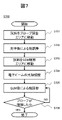
- FIG. 7 is a flow chart showing an example of the probe stylus process S700 in the defect inspection apparatus 100. As shown in FIG.
- the stage controller 165 controls the base stage controller 124 while confirming the optical image output by the camera image processor 163 so that the sample 131 and the probe 141 enter the probe adjustment area.
- the camera optical axis adjustment stage control unit 164 controls the camera optical axis adjustment stage 112 to adjust the optical axis of the camera 111 while confirming the optical image output by the camera image processing unit 163 .
- the stage control unit 165 controls the sample stage controller 126 and the probe unit controller 144 so that the distance between the sample 131 and the probe 141 is as short as possible. Control. Details of this step will be described later.
- Stage controller 165 controls base stage controller 124 so that sample 131 and probe 141 enter the SEM observation area.
- the electron beam column controller 161 controls the electron beam column controller 102 while checking the signal from the detector signal processor 162 to adjust the optical axis of the electron beam of the electron beam column 101 .
- the stage controller 165 controls the probe unit controller 144 to bring the sample 131 and the probe 141 closer to each other while checking the SEM image output by the detector signal processor 162 .
- the stage control unit 165 controls the approach speed to decrease as the separation distance between the sample 131 and the probe 141 decreases. To grasp the separation distance, the shadow of the probe 141 projected onto the sample 131 may be checked, or the difference between the focus positions of the sample 131 and the probe 141 in the SEM image may be used.
- FIG. 8 shows an SEM image (schematic diagram) output by the detector signal processing unit 162 in step S705.
- a structure 801 to be measured is included on the surface of the sample 131 .
- the structure 801 to be measured is a plug, which is connected to electrodes such as the gate, source, and drain of a transistor formed under the plug forming layer.
- the stage controller 165 controls the probe unit controller 144 and horizontally moves each probe 141 so that the tip of the probe 141 and the structure 801 to be measured overlap in the image.
- step S706 While confirming the SEM image output by the detector signal processing unit 162, the stage control unit 165 controls the probe unit controller 144, lowers the probe 141, and determines whether the probe 141 is in contact with the target structure 801 to be measured. do. If so, the sample contacting process S700 ends; if not, step S705 is executed again.
- the behavior of the tip of the probe 141 sliding on the surface of the structure to be measured 801 after the stylus may be detected from an SEM image.
- Approach to object 801 and changes in electrical properties caused by the stylus may be detected.
- the probe stylus process S700 is executed when the inspection position of the sample 131 or the sample 131 itself is changed, and when the sample stage 125 is driven for inspection by changing the working distance of the electron beam by the electron beam column 101. do.
- the case of changing the working distance of the electron beam is, for example, the case of changing the accelerating voltage of the electron beam. Since the information contained in the SEM image can be changed by changing the optical conditions such as the acceleration voltage, the optical conditions of the electron optical system may differ depending on the inspection.
- 4 to 6 are optical images captured by the side observation camera 111A.
- the appearance of the positional relationship between the sample 131 and the probe 141 in the optical image differs depending on the height of the optical axis of the side observation camera 111A.
- 4 shows the case where the optical axis of the side observation camera 111A is at the same height as the sample surface 401
- FIG. FIG. 6 shows the case where the optical axis of the side observation camera 111A is located at a position lower than the sample surface 401.
- the sample end 501 closer to the side observation camera 111A of the sample 131 and the sample end 502 farther from the side observation camera 111A are It can be confirmed in the acquired image of the side observation camera 111A.
- the optical axis of the side observation camera 111A coincides with the sample surface 401 (FIG. 4) or is located at a lower position (FIG. 6)
- the side observation camera of the sample 131 Only the sample edge 501 on the side closer to 111A can be confirmed in the acquired image of the side observation camera 111A.
- the height of the optical axis of the side observation camera 111A is adjusted based on the positional relationship between the sample ends 501 and 502 in the state shown in FIG.
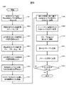
- FIG. 9 is a flow chart showing an example of step S702 in the probe stylus process S700 (FIG. 7), that is, a rough adjustment process using an optical image.
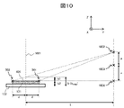
- FIG. 10 is a side view showing a camera position alignment method in a coarse adjustment process using an optical image.
- the projection plane of the camera is a plane located at a focal length away from the optical center of the camera and perpendicular to the optical axis. It is assumed that effects such as lens distortion have been canceled in advance by camera calibration.
- stage control unit 165 While confirming the optical image of the top observation camera 111B output by the camera image processing unit 163, the stage control unit 165 controls the base stage controller 124 so that the center position of the sample 131 coincides with the projection plane 1001 of the side observation camera 111A. to control.
- the camera optical axis adjustment stage control unit 164 moves the side surface to a position where the sample surface 401 can be confirmed in the optical image as shown in FIG.
- the camera optical axis adjustment stage controller 113 is controlled so that the observation camera 111A is positioned.
- the side observation camera optical axis adjustment stage 112A is controlled such that the side observation camera 111A is at the highest position, or the sample 131 is aligned with the reference position designated in the optical image. It is assumed that the optical center of the side observation camera 111A after control is completed is positioned at the optical center position 1002 (FIG. 10).
- the camera image processing unit 163 recognizes the sample end 501 and the sample end 502 of the sample 131 from the optical image of the side observation camera 111A, and recognizes the optical image, that is, the sample end 501 and the sample end 502 on the projection plane of the side observation camera 111A. output the distance between
- the camera optical axis adjustment stage control unit 164 positions the side observation camera 111A at a position where the sample surface 401 can be confirmed in the optical image while confirming the optical image of the side observation camera 111A output by the camera image processing unit 163.
- the camera optical axis adjustment stage controller 113 is controlled so that the camera position is lowered by a certain amount from the camera position in step S902.
- the displacement a from the position of the side observation camera 111A in step S902 is output. It is assumed that the optical center of the side observation camera 111A after the control is completed is positioned at the optical center position 1003 .
- step S905 As in step S903, the camera image processing unit 163 recognizes the sample end 501 and the sample end 502 of the sample 131 from the optical image of the side observation camera 111A, and detects the sample end on the projection plane of the side observation camera 111A. The distance between 501 and the sample end 502 is output.
- the camera image processing unit 163 determines when the distance between the sample end 501 and the sample end 502 of the sample 131 becomes zero, that is, when the optical axis of the side observation camera 111A , and the optical center position 1004 of the side observation camera 111A when the sample surface 401 is aligned (state shown in FIG. 4).
- FIG. 10 shows an optical image based on the perspective projection camera model when the optical center of the side observation camera 111A is positioned at the optical center position 1002.
- FIG. The value of the separation distance b (b 1002 ) between the ends of the sample in the optical image (projection plane 1001) is calculated in step S903.
- the unknowns are the separation distance x between the optical center positions 1003 and 1004 and the separation distance d between the sample end 501 or the sample end 502 and the projection plane 1001. ), the distance x between the optical center positions 1003 and 1004 can be calculated.
- the above calculation method is an example.
- the separation distance d between the sample end 501 (sample end 502) and the projection plane 1001 is known in advance, or the optical image of the top observation camera 111B output by the camera image processing unit 163 is used to measure the separation distance d.
- the distance between the optical center positions 1002 and 1004 can be calculated without executing steps S904 and S905.
- the optical axis of the side observation camera 111A, the horizontal drive surface of the sample stage 125, the upper surface of the sample holder 132, and the surface of the sample 131 are not strictly parallel to each other as shown in FIG. It may not be. In this case, the influence of these errors can be incorporated by calculating the optical center position 1004 based on the separation distances between the sample ends 501 and 502 at more than two optical center positions.
- the camera optical axis adjustment stage controller 164 controls the camera optical axis adjustment stage controller 113 so that the optical center of the side observation camera 111A matches the optical center position 1004 output in step S906.
- the height of the optical axis of the side observation camera 111A is aligned with the sample surface 401, it becomes easier to check the separation distance between the tip of the probe 141 and the sample 131, and it becomes easier to bring the probe 141 closer to the sample 131.
- the stage control unit 165 controls the sample stage controller 126 while confirming the optical image of the top observation camera 111B output by the camera image processing unit 163 so that the observation target portion of the sample 131 is included in the image.
- the stage control unit 165 controls the probe unit controller 144 so that the tip of the probe 141 is positioned at the observation target portion of the sample 131 while checking the optical image of the top observation camera 111B output by the camera image processing unit 163. do.
- the stage control unit 165 confirms the optical image of the side observation camera 111A output by the camera image processing unit 163, and adjusts the multiple probes 141 in the optical image.
- the probe unit controller 144 is controlled so that the heights of the probes 141 are kept constant.
- the stage control unit 165 controls the sample stage controller 126 so that the sample 131 approaches the probe 141 while confirming the optical image of the side observation camera 111A output by the camera image processing unit 163 .
- the camera optical axis adjustment stage controller 164 controls the camera optical axis adjustment stage controller 113 so that the optical axis of the side observation camera 111A moves along with the movement of the sample surface 401.
- the stage controller 165 controls the probe unit controller 144 to bring the probe 141 closer to the sample 131 while confirming the optical image of the side observation camera 111A output by the camera image processor 163 .
- the camera image processing unit 163 determines whether the probe 141 and the sample 131 are sufficiently close to each other. If sufficient rough alignment has been achieved, the rough adjustment process S702 using the optical image ends. If the rough alignment is not sufficient, steps S908 to S912 are executed again.
- steps S901 to S907 for aligning the height of the optical axis of the side observation camera 111A with the sample surface 401 may be repeated at any timing as necessary.
- the camera optical axis adjustment stage control unit 164 changes the optical image of the side observation camera 111A output by the camera image processing unit 163 from the state in which the sample surface 401 can be confirmed in the optical image (FIG. 5). , and the side observation camera optical axis adjustment stage 112A is controlled so as to stop the side observation camera 111A at the position where the sample end 501 and the sample end 502 overlap in the optical image. good too.
- the side observation camera optical axis adjustment stage 112A is adjusted based on the height information obtained by the sample height measuring unit. may be controlled.
- the side observation camera optical axis adjustment stage 112A is used to align the height of the optical axis of the side observation camera 111A with the sample surface.
- the side observation camera 111A is fixed to the sample chamber 121 and the base stage 122 can be moved vertically as well as horizontally.
- the probe 141 is a minute member as described above, the base stage 122 must be able to move up and down while the probe 141 and the sample 131 are in close proximity to each other without giving a large vibration or the like. It is difficult to implement in practice.
- the side observation camera optical axis adjustment stage 112A by using the side observation camera optical axis adjustment stage 112A, the positional relationship between the sample 131 and the probe 141 in the optical image can be adjusted without moving the sample 131 and the probe 141.
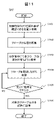
- FIG. 11 is a flowchart illustrating an example of a multiple probe proximity process S912.
- FIG. 12 is an optical image captured by the side observation camera 111A.
- the positional relationship of each probe is the state after adjustment in step S1103.
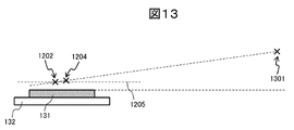
- FIG. 13 is a side view showing the positional relationship of each probe in step S1103.
- the camera optical axis adjustment stage control unit 164 adjusts the optical axis of the side observation camera 111A so that the height of the optical axis of the side observation camera 111A is aligned with the height of the sample surface 401.
- the adjustment stage 112A may be controlled, or may remain at a position higher than the sample surface 401 in step S1101.
- the stage controller 165 controls the probe unit controller 144 to bring the probe 1201 closer to the sample 131 while confirming the optical image of the side observation camera 111A output by the camera image processor 163 . At this time, the stage controller 165 also controls the probe 1203 in synchronization with the control of the probe 1201 to lower the probe 1203 by the same amount as the probe 1201 is lowered.
- the probe 141 that first contacts the sample 131 is the probe 1201 that is farthest from the side observation camera 111A, so the risk of other probes 1203 colliding with the sample surface 401 can be suppressed. Moreover, since a plurality of probes 141 can be brought close to the sample 131 at the same time, the throughput of the process can be improved.
- step S1105 The camera image processing unit 163 determines whether the probe 1201 and the sample 131 are sufficiently close to each other based on the optical image of the side observation camera 111A. If sufficient rough alignment has been achieved, the process advances to step S1106. If the rough alignment is not sufficient, step S1104 is executed again.
- the stage controller 165 controls the probe unit controller 144 to bring the probe 1203 closer to the sample 131 while confirming the optical image of the side observation camera 111A output by the camera image processor 163 .
- steps S1102 to S1105 may be repeatedly executed.
- a probe positional relationship acquisition process using a top observation camera will be described with reference to FIGS.
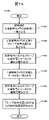
- the method can be applied, for example, in step S912 in the optical image coarse adjustment process (FIG. 9) to bring the probe 141 closer to the sample 131 .
- FIG. 14 is a flowchart showing an example of a probe positional relationship acquisition process using a top observation camera.
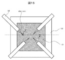
- 15 is an optical image captured by the top observation camera 111B
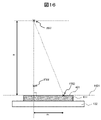
- FIG. 16 is a front view showing the positional relationship between the probe 1501 and the marker 1503 in steps S1402 to S1403
- FIG. 1405 is a front view showing the positional relationship between the probe 1501 and the marker 1503 in S1405.
- the marker 1503 is a peculiar structure or a special mark on the sample surface 401 that can be confirmed in an optical image, and may be a foreign matter adhering to the sample surface 401 .
- the projection plane of the camera is a plane located at a focal length away from the optical center of the camera and perpendicular to the optical axis. It is assumed that effects such as lens distortion have been canceled in advance by camera calibration.
- the stage controller 165 controls the sample stage controller 126 so that the projection plane 1601 of the top observation camera 111B matches the sample surface 401 while checking the optical image of the top observation camera 111B output by the camera image processing unit 163. Control.
- the camera optical axis adjustment stage 112B is vertically movable, the camera optical axis is adjusted by the camera optical axis adjustment stage controller 164 so that the projection plane 1601 of the top observation camera 111B coincides with the sample plane 401.
- a stage controller 113 may be controlled.
- the top observation camera 111B is controlled within a plane parallel to the sample surface 401. Therefore, in subsequent steps, the projection plane 1601 and the sample plane 401 match.
- the camera optical axis adjustment stage control unit 164 adjusts the optical axis of the top observation camera 111B and the probe tip position 1502 of the probe 1501 in the optical image.
- the camera optical axis adjustment stage controller 113 is controlled so that .
- the optical center of the top observation camera 111B after control is completed is positioned at the optical center position 1602 (FIG. 16).
- the camera image processing unit 163 outputs the optical image, that is, the separation distance m1 between the probe tip position 1502 and the marker 1503 on the projection plane of the top observation camera 111B from the optical image of the top observation camera 111B.
- the camera optical axis adjustment stage control unit 164 confirms the optical image of the top observation camera 111B output by the camera image processing unit 163, and adjusts the optical axis of the top observation camera 111B to match the marker 1503 in the optical image. Then, the camera optical axis adjustment stage controller 113 is controlled. The optical center of the top observation camera 111B after control is completed is positioned at the optical center position 1701 (FIG. 17). The camera optical axis adjustment stage control unit 164 outputs the movement amount m2 of the optical axis of the top observation camera 111B from step S1402.
- the camera image processing unit 163 outputs the optical image , that is, the separation distance m3 between the probe tip position 1502 and the marker 1503 on the projection plane of the top observation camera 111B from the optical image of the top observation camera 111B.
- the camera image processing unit 163 outputs the distance (vertical distance) of the probe tip position 1502 in the direction perpendicular to the sample surface 401 based on the values output in steps S1403 and S1405.
- FIG. 17 shows an optical image based on the perspective projection camera model when the optical center of the top observation camera 111B is positioned at the optical center position 1701.
- FIG. 17 shows an optical image based on the perspective projection camera model when the optical center of the top observation camera 111B is positioned at the optical center position 1701.
- the distance (vertical distance) of the probe tip position 1502 in the direction perpendicular to the sample surface 401 (vertical distance) is H 2 and the focal length of the camera is H, the following relationship holds.
- Rough alignment of the probe 1501 may be executed based on the vertical distance between the probe tip position 1502 and the sample surface 401 output in step S1406, or the absolute position coordinates of the probe tip position 1502 or the marker 1503 may be calculated.
- the separation distance m1 calculated in step S1403 is equal to the movement amount m2 of the optical axis of the top observation camera 111B, which is the output of step S1404. Therefore, the movement amount m2 may be used without obtaining the separation distance m1 from the optical image.
- the probe tip position 1502 and the marker 1503 are positioned on the horizontal line (indicated by the dotted line in FIG. 15) in the optical image of the top observation camera 111B. It works in any direction.
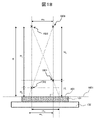
- FIG. 18 is a front view showing the positional relationship between tip positions 1502 and 1801 of two probes.
- the flow of FIG. 14 is executed by replacing the marker 1503 with the tip position 1801 of the probe.
- the optical center of the top observation camera 111B when the optical axis of the top observation camera 111B coincides with the probe tip position 1801 in the optical image is located at the optical center position 1802 (FIG. 18).
- the distance ( vertical distance) in the direction perpendicular to the sample surface 401 of the probe tip position 1801 is H4, the following relationship holds.
- H1 H x ( m2 / m3)
- H3 H x ( m2 / m1)
- step S1401 another marker is set on the sample surface 401 in addition to the marker 1503, and the separation distance m ⁇ between the markers on the optical image and the optical axis of the top observation camera 111B in the optical image are measured.
- the separation distance m ⁇ between the optical centers of the top observation camera 111B when each marker matches the projection surface 1601 of the top observation camera 111B and the sample surface 401 are regarded as matching, and a match determination is performed. can be done.
- the top observation camera optical axis adjustment stage 112B is used in order to move the optical axis of the top observation camera 111B onto the tip positions of the markers and probes.
- the top observation camera 111B is fixed to the sample chamber 121, and the stage controller 165 controls the sample stage controller 126 to move the marker 1503, or the stage controller 165 moves the probe tip position 1502.
- a flow of controlling the probe unit controller 144 to allow the flow is also conceivable.
- a flow in which the stage controller 165 controls the base stage controller 124 to horizontally move the base stage 122 is also conceivable.
- this flow has the advantage of being able to adjust the position of the optical axis in the optical image without moving the sample 131 and the probe 141 by using the top observation camera optical axis adjustment stage 112B.
- 101 electron beam column, 102: electron beam column controller, 103: charged particle detector, 104: controller for charged particle detector, 111: camera, 111A: side observation camera, 111B: top observation camera, 112: camera light Axis adjustment stage 112A: Side observation camera optical axis adjustment stage 112B: Top observation camera optical axis adjustment stage 113: Camera optical axis adjustment stage controller 121: Sample chamber 122: Base stage 123: Base stage guide 124: Base stage controller, 125: Sample stage, 126: Sample stage controller, 127: Sample holder receiver, 131: Sample, 132: Sample holder, 141, 1201, 1203, 1501: Probe, 142: Probe holder, 143 : probe unit, 144: probe unit controller, 145: probe unit support, 151: control computer, 152: input device, 153: display, 161: electron beam column controller, 162: detector signal processor, 163: Camera image processing unit 164: camera optical axis adjustment stage control unit 165: stage control unit 401: sample
Landscapes
- Physics & Mathematics (AREA)
- General Physics & Mathematics (AREA)
- Engineering & Computer Science (AREA)
- Computer Vision & Pattern Recognition (AREA)
- Theoretical Computer Science (AREA)
- Testing Or Measuring Of Semiconductors Or The Like (AREA)
- Analysing Materials By The Use Of Radiation (AREA)
- Testing Of Individual Semiconductor Devices (AREA)
Priority Applications (4)
| Application Number | Priority Date | Filing Date | Title |
|---|---|---|---|
| PCT/JP2021/024581 WO2023276002A1 (ja) | 2021-06-29 | 2021-06-29 | プローブ装置 |
| US18/566,151 US12461126B2 (en) | 2021-06-29 | 2021-06-29 | Probe device |
| JP2023531203A JP7614351B2 (ja) | 2021-06-29 | 2021-06-29 | プローブ装置 |
| TW111121396A TWI832284B (zh) | 2021-06-29 | 2022-06-09 | 探針裝置 |
Applications Claiming Priority (1)
| Application Number | Priority Date | Filing Date | Title |
|---|---|---|---|
| PCT/JP2021/024581 WO2023276002A1 (ja) | 2021-06-29 | 2021-06-29 | プローブ装置 |
Publications (1)
| Publication Number | Publication Date |
|---|---|
| WO2023276002A1 true WO2023276002A1 (ja) | 2023-01-05 |
Family
ID=84689790
Family Applications (1)
| Application Number | Title | Priority Date | Filing Date |
|---|---|---|---|
| PCT/JP2021/024581 Ceased WO2023276002A1 (ja) | 2021-06-29 | 2021-06-29 | プローブ装置 |
Country Status (4)
| Country | Link |
|---|---|
| US (1) | US12461126B2 (cg-RX-API-DMAC7.html) |
| JP (1) | JP7614351B2 (cg-RX-API-DMAC7.html) |
| TW (1) | TWI832284B (cg-RX-API-DMAC7.html) |
| WO (1) | WO2023276002A1 (cg-RX-API-DMAC7.html) |
Cited By (1)
| Publication number | Priority date | Publication date | Assignee | Title |
|---|---|---|---|---|
| CN116560062A (zh) * | 2023-07-10 | 2023-08-08 | 南京凯视迈科技有限公司 | 显微镜对焦防碰撞控制方法 |
Families Citing this family (1)
| Publication number | Priority date | Publication date | Assignee | Title |
|---|---|---|---|---|
| DE102024135697A1 (de) * | 2024-12-02 | 2026-06-03 | Carl Zeiss Microscopy Gmbh | Verfahren zum Annähern einer Mikrokontaktnadel entlang einer Annäherungsrichtung an ein Annäherungszielobjekt und Teilchenstrahlmikroskop |
Citations (5)
| Publication number | Priority date | Publication date | Assignee | Title |
|---|---|---|---|---|
| JP2006093102A (ja) * | 2004-08-25 | 2006-04-06 | Sii Nanotechnology Inc | プローブのアプローチ方法および荷電粒子ビーム装置 |
| JP2006294481A (ja) * | 2005-04-13 | 2006-10-26 | Hitachi High-Technologies Corp | 荷電粒子線装置 |
| JP2013243027A (ja) * | 2012-05-21 | 2013-12-05 | Hitachi High-Technologies Corp | 荷電粒子線装置 |
| JP2018084582A (ja) * | 2016-11-22 | 2018-05-31 | アントン パール ゲーエムベーハーAnton Paar GmbH | 実質的に水平な側方視で、走査型プローブ顕微鏡の試料とプローブとの間のギャップを撮像する走査型プローブ顕微鏡及び方法 |
| JP2019035741A (ja) * | 2017-08-11 | 2019-03-07 | アントン パール ゲーエムベーハーAnton Paar GmbH | 側面視撮像による試料の高さプロファイルの特性評価 |
Family Cites Families (13)
| Publication number | Priority date | Publication date | Assignee | Title |
|---|---|---|---|---|
| US4864227A (en) * | 1987-02-27 | 1989-09-05 | Canon Kabushiki Kaisha | Wafer prober |
| JPH03209737A (ja) * | 1990-01-11 | 1991-09-12 | Tokyo Electron Ltd | プローブ装置 |
| JPH0534143A (ja) | 1991-07-29 | 1993-02-09 | Tokyo Seimitsu Co Ltd | 試料表面のモニタ装置及びその方法 |
| US5394100A (en) * | 1993-05-06 | 1995-02-28 | Karl Suss America, Incorporated | Probe system with automatic control of contact pressure and probe alignment |
| JP2003315238A (ja) | 2002-04-26 | 2003-11-06 | Jeol Ltd | 測定位置合わせ方法、カンチレバ及び走査形プローブ顕微鏡 |
| DE10220343B4 (de) * | 2002-05-07 | 2007-04-05 | Atg Test Systems Gmbh & Co. Kg Reicholzheim | Vorrichtung und Verfahren zum Prüfen von Leiterplatten und Prüfsonde |
| JP4675615B2 (ja) | 2003-12-05 | 2011-04-27 | 株式会社日立ハイテクノロジーズ | 不良検査装置並びにプローブ位置決め方法およびプローブ移動方法 |
| DE102004058483B4 (de) | 2003-12-05 | 2009-12-17 | Hitachi High-Technologies Corp. | Vorrichtung zur Untersuchung von Produkten auf Fehler, Messfühler-Positionierverfahren und Messfühler-Bewegungsverfahren |
| JP4993849B2 (ja) | 2004-05-31 | 2012-08-08 | 株式会社日立ハイテクノロジーズ | 不良検査装置及び荷電粒子線装置 |
| JP5860642B2 (ja) | 2011-09-07 | 2016-02-16 | 株式会社日立ハイテクノロジーズ | 走査電子顕微鏡 |
| JP6009862B2 (ja) | 2012-08-24 | 2016-10-19 | 株式会社日立ハイテクサイエンス | 走査型プローブ顕微鏡 |
| JP7204200B2 (ja) | 2019-02-14 | 2023-01-16 | 株式会社日立ハイテクサイエンス | 薄膜試料片作成方法および荷電粒子ビーム装置 |
| EP4118674A1 (en) * | 2020-03-13 | 2023-01-18 | Carl Zeiss SMT GmbH | Method of cross-section imaging of an inspection volumes in wafer |
-
2021
- 2021-06-29 US US18/566,151 patent/US12461126B2/en active Active
- 2021-06-29 JP JP2023531203A patent/JP7614351B2/ja active Active
- 2021-06-29 WO PCT/JP2021/024581 patent/WO2023276002A1/ja not_active Ceased
-
2022
- 2022-06-09 TW TW111121396A patent/TWI832284B/zh active
Patent Citations (5)
| Publication number | Priority date | Publication date | Assignee | Title |
|---|---|---|---|---|
| JP2006093102A (ja) * | 2004-08-25 | 2006-04-06 | Sii Nanotechnology Inc | プローブのアプローチ方法および荷電粒子ビーム装置 |
| JP2006294481A (ja) * | 2005-04-13 | 2006-10-26 | Hitachi High-Technologies Corp | 荷電粒子線装置 |
| JP2013243027A (ja) * | 2012-05-21 | 2013-12-05 | Hitachi High-Technologies Corp | 荷電粒子線装置 |
| JP2018084582A (ja) * | 2016-11-22 | 2018-05-31 | アントン パール ゲーエムベーハーAnton Paar GmbH | 実質的に水平な側方視で、走査型プローブ顕微鏡の試料とプローブとの間のギャップを撮像する走査型プローブ顕微鏡及び方法 |
| JP2019035741A (ja) * | 2017-08-11 | 2019-03-07 | アントン パール ゲーエムベーハーAnton Paar GmbH | 側面視撮像による試料の高さプロファイルの特性評価 |
Cited By (2)
| Publication number | Priority date | Publication date | Assignee | Title |
|---|---|---|---|---|
| CN116560062A (zh) * | 2023-07-10 | 2023-08-08 | 南京凯视迈科技有限公司 | 显微镜对焦防碰撞控制方法 |
| CN116560062B (zh) * | 2023-07-10 | 2023-10-03 | 南京凯视迈科技有限公司 | 显微镜对焦防碰撞控制方法 |
Also Published As
| Publication number | Publication date |
|---|---|
| TWI832284B (zh) | 2024-02-11 |
| JPWO2023276002A1 (cg-RX-API-DMAC7.html) | 2023-01-05 |
| TW202300931A (zh) | 2023-01-01 |
| US20240288472A1 (en) | 2024-08-29 |
| JP7614351B2 (ja) | 2025-01-15 |
| US12461126B2 (en) | 2025-11-04 |
Similar Documents
| Publication | Publication Date | Title |
|---|---|---|
| JP5941704B2 (ja) | パターン寸法測定装置、及びコンピュータプログラム | |
| JP5525953B2 (ja) | 寸法測定装置、寸法測定方法及び寸法測定装置用のプログラム | |
| KR102615578B1 (ko) | 사이드 뷰 이미징을 사용하는 시료의 높이 프로파일 특성화 | |
| JP5788719B2 (ja) | ステージ装置およびステージ装置の制御方法 | |
| CN120748994A (zh) | 用于聚焦带电粒子束的系统和方法 | |
| JP2018004497A (ja) | 画像測定装置 | |
| JP2018004496A (ja) | 画像測定装置 | |
| CN103180691A (zh) | 形状测定装置、形状测定方法、构造物的制造方法及程序 | |
| CN111239164B (zh) | 一种缺陷检测装置及其方法 | |
| JP5467962B2 (ja) | 測定設定データ作成装置、測定設定データ作成方法、測定設定データ作成装置用のプログラム及び寸法測定装置 | |
| JP7614351B2 (ja) | プローブ装置 | |
| CN109425320B (zh) | 表面纹理测量设备的控制方法 | |
| JP2012037257A (ja) | 測定設定データ作成装置、測定設定データ作成方法及び測定設定データ作成装置用のプログラム | |
| KR102165735B1 (ko) | 화상 처리 장치, 자기 조직화 리소그래피 기술에 의한 패턴 생성 방법 및 컴퓨터 프로그램 | |
| JPWO2017033591A1 (ja) | 荷電粒子線装置および試料ステージのアライメント調整方法 | |
| WO2010089960A1 (ja) | 電子線の影響を考慮した半導体検査方法及び装置 | |
| JP6203502B2 (ja) | 加工品に対して加工工具を位置決めするための構造および方法 | |
| US20140312224A1 (en) | Pattern inspection method and pattern inspection apparatus | |
| JP2007018935A (ja) | プローブ付き顕微鏡及びプローブ接触方法 | |
| JP2007183184A (ja) | 倣いプローブの校正方法 | |
| JP4133657B2 (ja) | 精密計測用x線透視装置 | |
| JP2011033422A (ja) | 検査装置及び検査方法 | |
| JP2004077423A (ja) | 試料像測長方法及び試料像測長装置 | |
| JP5202568B2 (ja) | 半導体検査装置及びそのコンピュータプログラム | |
| JP2008060505A (ja) | 半導体検査方法及び装置 |
Legal Events
| Date | Code | Title | Description |
|---|---|---|---|
| 121 | Ep: the epo has been informed by wipo that ep was designated in this application |
Ref document number: 21948310 Country of ref document: EP Kind code of ref document: A1 |
|
| WWE | Wipo information: entry into national phase |
Ref document number: 18566151 Country of ref document: US |
|
| WWE | Wipo information: entry into national phase |
Ref document number: 2023531203 Country of ref document: JP |
|
| NENP | Non-entry into the national phase |
Ref country code: DE |
|
| 122 | Ep: pct application non-entry in european phase |
Ref document number: 21948310 Country of ref document: EP Kind code of ref document: A1 |
|
| WWG | Wipo information: grant in national office |
Ref document number: 18566151 Country of ref document: US |