WO2023248670A1 - 半導体装置、電力変換装置、および、半導体装置の製造方法 - Google Patents
半導体装置、電力変換装置、および、半導体装置の製造方法 Download PDFInfo
- Publication number
- WO2023248670A1 WO2023248670A1 PCT/JP2023/018941 JP2023018941W WO2023248670A1 WO 2023248670 A1 WO2023248670 A1 WO 2023248670A1 JP 2023018941 W JP2023018941 W JP 2023018941W WO 2023248670 A1 WO2023248670 A1 WO 2023248670A1
- Authority
- WO
- WIPO (PCT)
- Prior art keywords
- insulating film
- protective insulating
- semiconductor device
- semiconductor
- electrode layer
- Prior art date
- Legal status (The legal status is an assumption and is not a legal conclusion. Google has not performed a legal analysis and makes no representation as to the accuracy of the status listed.)
- Ceased
Links
Images


Classifications
-
- H—ELECTRICITY
- H10—SEMICONDUCTOR DEVICES; ELECTRIC SOLID-STATE DEVICES NOT OTHERWISE PROVIDED FOR
- H10D—INORGANIC ELECTRIC SEMICONDUCTOR DEVICES
- H10D62/00—Semiconductor bodies, or regions thereof, of devices having potential barriers
- H10D62/80—Semiconductor bodies, or regions thereof, of devices having potential barriers characterised by the materials
- H10D62/83—Semiconductor bodies, or regions thereof, of devices having potential barriers characterised by the materials being Group IV materials, e.g. B-doped Si or undoped Ge
- H10D62/832—Semiconductor bodies, or regions thereof, of devices having potential barriers characterised by the materials being Group IV materials, e.g. B-doped Si or undoped Ge being Group IV materials comprising two or more elements, e.g. SiGe
- H10D62/8325—Silicon carbide
-
- H—ELECTRICITY
- H10—SEMICONDUCTOR DEVICES; ELECTRIC SOLID-STATE DEVICES NOT OTHERWISE PROVIDED FOR
- H10W—GENERIC PACKAGES, INTERCONNECTIONS, CONNECTORS OR OTHER CONSTRUCTIONAL DETAILS OF DEVICES COVERED BY CLASS H10
- H10W74/00—Encapsulations, e.g. protective coatings
- H10W74/10—Encapsulations, e.g. protective coatings characterised by their shape or disposition
- H10W74/131—Encapsulations, e.g. protective coatings characterised by their shape or disposition the semiconductor body being only partially enclosed
- H10W74/137—Encapsulations, e.g. protective coatings characterised by their shape or disposition the semiconductor body being only partially enclosed the encapsulations being directly on the semiconductor body
-
- H—ELECTRICITY
- H10—SEMICONDUCTOR DEVICES; ELECTRIC SOLID-STATE DEVICES NOT OTHERWISE PROVIDED FOR
- H10D—INORGANIC ELECTRIC SEMICONDUCTOR DEVICES
- H10D8/00—Diodes
- H10D8/01—Manufacture or treatment
- H10D8/051—Manufacture or treatment of Schottky diodes
-
- H—ELECTRICITY
- H10—SEMICONDUCTOR DEVICES; ELECTRIC SOLID-STATE DEVICES NOT OTHERWISE PROVIDED FOR
- H10D—INORGANIC ELECTRIC SEMICONDUCTOR DEVICES
- H10D8/00—Diodes
- H10D8/60—Schottky-barrier diodes
-
- H—ELECTRICITY
- H10—SEMICONDUCTOR DEVICES; ELECTRIC SOLID-STATE DEVICES NOT OTHERWISE PROVIDED FOR
- H10W—GENERIC PACKAGES, INTERCONNECTIONS, CONNECTORS OR OTHER CONSTRUCTIONAL DETAILS OF DEVICES COVERED BY CLASS H10
- H10W74/00—Encapsulations, e.g. protective coatings
- H10W74/01—Manufacture or treatment
-
- H—ELECTRICITY
- H10—SEMICONDUCTOR DEVICES; ELECTRIC SOLID-STATE DEVICES NOT OTHERWISE PROVIDED FOR
- H10W—GENERIC PACKAGES, INTERCONNECTIONS, CONNECTORS OR OTHER CONSTRUCTIONAL DETAILS OF DEVICES COVERED BY CLASS H10
- H10W90/00—Package configurations
Definitions
- the technology disclosed in this specification relates to a technology for increasing the reliability of a semiconductor device.
- semiconductor devices as shown in Patent Document 1 particularly insulated gate bipolar transistors (IGBTs), metal-oxide-semiconductor field-effect transistors (metal-oxide-semiconductor field-effect transistors), etc. transistor
- IGBTs insulated gate bipolar transistors
- metal-oxide-semiconductor field-effect transistors metal-oxide-semiconductor field-effect transistors
- MOSFETs metal-oxide-semiconductor field-effect transistors
- SBDs Schottky barrier diodes
- the technology disclosed in the present specification was developed in view of the problems described above, and is a technology for improving the reliability of semiconductor devices.
- a semiconductor device that is a first aspect of the technology disclosed in the present specification includes a semiconductor layer, a first electrode layer that covers a part of the upper surface of the semiconductor layer, and another part of the upper surface of the semiconductor layer. and an insulating film covering a part of the upper surface of the first electrode layer, the arithmetic mean roughness of the upper surface of the insulating film being the arithmetic mean roughness of the interface between the insulating film and the first electrode layer. Less than average roughness.
- connection with the component below the protective insulating film is made stronger than the connection with the component above the protective insulating film. Therefore, peeling of the protective insulating film during operation can be suppressed. According to such a configuration, the reliability of the semiconductor device can be improved.
- FIG. 1 is a diagram schematically showing an example of the configuration of a semiconductor device manufactured by the manufacturing method described in the embodiments.
- 1 is a diagram schematically showing an example of the configuration of a semiconductor device manufactured by the manufacturing method described in the embodiments.
- 1 is a diagram schematically showing an example of the configuration of a semiconductor device manufactured by the manufacturing method described in the embodiments.
- 3 is a flowchart illustrating an example of a manufacturing process of a SiC-SBD according to an embodiment.
- FIG. 3 is a cross-sectional view showing an example of a manufacturing process of a SiC-SBD according to an embodiment.
- FIG. 3 is a cross-sectional view showing an example of a manufacturing process of a SiC-SBD according to an embodiment.
- FIG. 3 is a cross-sectional view showing an example of a manufacturing process of a SiC-SBD according to an embodiment.
- FIG. 3 is a cross-sectional view showing an example of a manufacturing process of a SiC-SBD according to an embodiment.
- FIG. 3 is a cross-sectional view showing an example of a manufacturing process of a SiC-SBD according to an embodiment.
- FIG. 3 is a cross-sectional view showing an example of a manufacturing process of a SiC-SBD according to an embodiment.
- FIG. 3 is a cross-sectional view showing an example of a manufacturing process of a SiC-SBD according to an embodiment.
- FIG. 3 is a cross-sectional view showing an example of a manufacturing process of a SiC-SBD according to an embodiment.
- FIG. 3 is a cross-sectional view showing an example of a manufacturing process of a SiC-SBD according to an embodiment.
- FIG. 3 is a cross-sectional view showing an example of a manufacturing process of a SiC-SBD according to an embodiment.
- FIG. 2 is an enlarged view showing the structure near a surface electrode and a protective insulating film of a semiconductor device in an embodiment.
- FIG. 3 is a diagram showing the definition of arithmetic mean roughness.
- FIG. 7 is a diagram showing the relationship between the ratio of the arithmetic mean roughness of the upper and lower surfaces of the protective insulating film and the peeling rate of the protective insulating film after performing a power cycle test 100,000 times.
- the vertices formed at the end of the upper surface of the protective insulating film we focus on the vertex with the smallest angle, and when the ratio of the arithmetic mean roughness of the upper and lower surfaces of the protective insulating film is 0.7, FIG.
- 3 is a diagram showing the relationship between angle and crack occurrence rate.
- 1 is a diagram schematically showing an example of the configuration of a semiconductor device manufactured by the manufacturing method described in the embodiments.
- 1 is a diagram schematically showing an example of the configuration of a semiconductor device manufactured by the manufacturing method described in the embodiments.
- 1 is a diagram schematically showing an example of a configuration of a semiconductor device manufactured by a manufacturing method described in an embodiment.
- 3 is a flowchart illustrating an example of a manufacturing process of a SiC-SBD according to an embodiment.
- 21 is a cross-sectional view showing an example of the structure of a semiconductor device in which steps up to step ST06 in FIG. 20 have been completed;
- FIG. It is a flow chart showing an example of plating pretreatment and plating treatment.
- FIG. 2 is a diagram showing an example of the structure of a semiconductor device.
- FIG. 2 is a diagram showing an example of the structure of a semiconductor device.
- FIG. 2 is a diagram showing an example of the structure of a semiconductor device.
- FIG. 2 is a diagram showing an example of the structure of a semiconductor device.
- FIG. 3 is a diagram showing the relationship between the difference between the interface between surface electrodes and the interface between surface electrodes and a protective insulating film, and the defective rate after an assembly test.
- 1 is a diagram schematically showing the configuration of a power conversion system to which a power conversion device according to an embodiment is applied.
- 1 is a diagram schematically showing an example of the configuration of a semiconductor device manufactured by the manufacturing method described in the embodiments.
- 1 is a diagram schematically showing an example of the configuration of a semiconductor device manufactured by the manufacturing method described in the embodiments.
- 1 is a diagram schematically showing an example of the configuration of a semiconductor device manufactured by the manufacturing method described in the embodiments.
- ordinal numbers such as “first” or “second” are sometimes used in the description of the present specification, these terms will not be used to facilitate understanding of the content of the embodiments. These ordinal numbers are used for convenience and the content of the embodiments is not limited to the order that can occur based on these ordinal numbers.
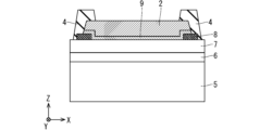
- ⁇ About the configuration of the semiconductor device> 1 2, and 3 are diagrams schematically showing an example of the structure of a semiconductor device manufactured by the manufacturing method described in this embodiment.
- a SiC-Schottky barrier diode (SBD) is shown.
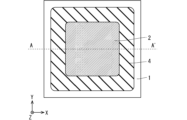
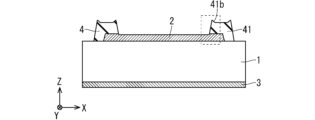
- FIG. 1 is a plan view of a SiC-SBD. As shown in FIG. 1, a surface electrode 2 is formed in the central current-carrying region, and a protective insulating film 4 is formed around it to ensure insulation from the surroundings.
- FIG. 2 is a cross-sectional view corresponding to the A-A' cross-section indicated by the broken line in FIG.
- a front electrode 2 is provided on the upper surface of the semiconductor substrate 1
- a back electrode 3 is provided on the lower surface of the semiconductor substrate 1 .
- each of the front electrode 2 and the back electrode 3 is wired to the outside by appropriate means such as wire or soldering.
- a protective insulating film 4 is provided on the outer periphery of the surface electrode 2 in order to suppress poor insulation of the semiconductor device due to discharge at the outer periphery of the chip.
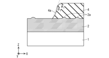
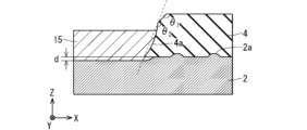
- FIG. 3 is an enlarged view of the area surrounded by the broken line in FIG. 2.
- a surface electrode 2 is formed on the upper surface of the semiconductor substrate 1 , and a protective insulating film 4 is further formed on the upper surface of the surface electrode 2 .
- the arithmetic mean roughness of the upper surface of the protective insulating film 4 is smaller than the arithmetic mean roughness of the interface between the protective insulating film 4 and the surface electrode 2 (that is, the lower surface of the protective insulating film 4).
- a plurality of vertices are provided at the upper end of the protective insulating film 4.
- FIG. 4 is a flowchart illustrating an example of the SiC-SBD manufacturing process according to this embodiment. Further, FIGS. 5 to 12 are cross-sectional views showing examples of the manufacturing process of the SiC-SBD according to this embodiment. Hereinafter, the manufacturing process of the SiC-SBD will be specifically explained with reference to FIGS. 5 to 12.
- a drift layer 6 made of n-type SiC is formed on the first main surface (hereinafter referred to as the surface) located on the positive Z-axis side of the n-type SiC substrate 5.
- a second drift layer 7 is formed by epitaxial crystal growth at a growth temperature lower than that of the drift layer 6 so as to be in contact with the upper surface of the drift layer 6. It is formed as a layered epitaxial film (corresponding to step ST01 in FIG. 4).
- an interlayer insulating film 8 is formed on the upper surface of the drift layer 7 by a deposition method such as a thermal oxidation method or a chemical vapor deposition method.
- a mask (not shown here) made of resist or the like is formed using photolithography, and unnecessary areas are removed by dry etching using plasma or wet etching using a chemical solution.
- the interlayer insulating film 8 is removed, and then the above-mentioned mask is removed by plasma ashing, wet processing, or the like.
- boron (B) or aluminum (Al) is used as the p-type impurity, and phosphorus is used as the n-type impurity, so that the desired breakdown voltage of the SiC-SBD can be obtained.
- An impurity layer is formed by ion implantation and activation using (P) or nitrogen (N) as appropriate.
- a Schottky electrode layer 9 is formed so as to be in contact with the drift layer 7 (corresponding to step ST02 in FIG. 4).
- the electrode material can be appropriately selected from titanium (Ti), nickel (Ni), iridium (Ir), platinum (Pt), etc.
- the electrode material formed in the excess portion of the outer peripheral area is removed by patterning using photolithography and etching using plasma or a chemical solution to ensure electrical connection between the drift layer 7 and the Schottky electrode layer 9. Heat treatment is performed as necessary. By doing so, a cross-sectional structure as shown in FIG. 8 is obtained.
- the surface electrode 2 is formed using aluminum, an aluminum alloy made of aluminum and silicon, nickel, or the like by sputtering or vapor deposition. Thereafter, it is removed by patterning by photolithography and etching using plasma or a chemical solution. Thereafter, by heating for 15 minutes or more at, for example, 150° C. or higher and 400° C. or lower, unevenness can be formed on the surface of the front electrode 2 (corresponding to step ST03 in FIG. 4).
- the surface electrode 2 is formed on a part of the upper surface of the drift layer 6 and the drift layer 7 via a Schottky electrode layer 9, an interlayer insulating film 8, and the like.
- a protective insulating film 4 is formed as shown in FIG.
- the material for the protective insulating film 4 is preferably polyimide or silicone resin, and these materials can be coated on the surface side of the SiC-SBD by using spin coating, photolithography, etching technology, or inkjet coating technology.
- a protective insulating film 4 is formed on the outermost periphery (corresponding to step ST04 in FIG. 4).
- the protective insulating film 4 covers a portion of the upper surface of the drift layer 7 that is not covered by the surface electrode 2 . Furthermore, the protective insulating film 4 covers a part of the upper surface of the front electrode 2 .
- a plurality of vertices are formed on the upper surface of the protective insulating film 4 by surface treatment using plasma containing oxygen and argon. At this time, if a plurality of vertices are also formed on the upper surface of the protective insulating film 4 on the outer peripheral side of the semiconductor device, reliability is further improved.
- a suitable processing method may be used as appropriate, such as repeating an inkjet coating technique multiple times or subsequently applying a heat treatment at 250° C. or higher. The method is selectable.
- heat treatment is performed at, for example, 200° C. or higher and 400° C. or lower, more preferably, 250° C. or higher and 380° C. or lower, so that the slope of the protective insulating film 4 is shaped as shown in FIG. 13, which will be described later.
- the shape is an arc as shown in the example. Note that the heat treatment after forming the above-mentioned surface electrode 2 can also be used as the heat treatment after forming the protective insulating film 4.
- the SiC substrate 5 is machined from the lower surface side using a grinding wheel made of alumina abrasive grains or diamond abrasive grains, for example.
- the SiC substrate 5 is made thinner (corresponding to step ST05 in FIG. 4). Note that the thinning (thinning) of the SiC substrate 5 can be omitted if necessary.
- the back electrode 3 is formed using titanium, a titanium alloy, aluminum, an aluminum alloy made of aluminum and silicon, nickel, or the like (corresponding to step ST06 in FIG. 4).
- an oxidation prevention film made of gold, platinum, silver, or a silver alloy containing palladium is formed on the outermost surface of the back electrode 3. Good too.
- the plurality of semiconductor devices formed on the semiconductor wafer are diced using a dicing device to obtain semiconductor devices as examples shown in FIGS. 1, 2, and 3.
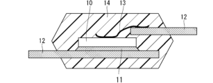
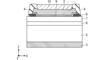
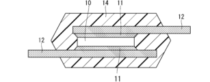
- the semiconductor device 10 manufactured as described above has, for example, an upper surface and a lower surface of the semiconductor device 10 with respect to the lead frame 12, for example, with the solder 11 and the wire 13. After being connected using molding resin 14, the semiconductor module is completed.
- FIG. 13 is an enlarged view showing the structure near the surface electrode 2 and protective insulating film 4 of the semiconductor device 10 in this embodiment.
- FIG. 14 is a diagram showing the definition of arithmetic mean roughness. As shown in FIG. 14, according to the definition of surface roughness (JIS B 0601:1994, JIS B 0031:1994), the arithmetic mean roughness Ra is calculated by measuring the reference length from the roughness curve 400 in the direction of the average line 401. It can be determined by the equation shown in the figure, with the direction of the average line of this sampled portion as the X axis and the direction of vertical magnification as the Y axis.
- the inventors performed a 1 mm line scan using an atomic force microscope (AFM) SPM-9600 manufactured by Shimadzu Corporation, obtained the above roughness curve 400, and then calculated the arithmetic mean roughness.
- the value Ra was calculated.
- you can select any method such as not only the above method but also a stylus-type step/surface roughness meter or a laser microscope that can measure non-contact. can.
- the arithmetic mean roughness of the upper surface of the protective insulating film 4 is smaller than the arithmetic mean roughness of the interface between the protective insulating film 4 and the surface electrode 2 (i.e., the lower surface of the protective insulating film 4).
- a plurality of convex portions 2a are formed on the upper surface of the surface electrode 2, which is one reason why the arithmetic mean roughness of the interface between the protective insulating film 4 and the surface electrode 2 increases. .
- a plurality of vertices are formed at the end of the upper surface of the protective insulating film 4.
- the end of the upper surface of the protective insulating film 4 is an inclined surface
- the apex formed at the upper end of the inclined surface has an obtuse angle ⁇ 1
- the apex formed at the lower end of the inclined surface has an obtuse angle ⁇ 1.
- the vertex has an obtuse angle ⁇ 2 .
- the ridgeline 4a on the side surface of the protective insulating film 4 is concave compared to a straight line drawn from the edge of the upper surface (specifically, the apex formed at the lower end of the inclined surface) to the edge (vertex) of the lower surface. It becomes the shape.
- the inventors conducted a power cycle test on a semiconductor module having the structure shown in FIG. 12, in which the semiconductor device was repeatedly energized and de-energized.
- the protective insulating film 4 resists stress due to thermal expansion or thermal contraction from the upper surface side due to the difference in linear expansion coefficient with the mold resin 14 and from the lower surface side due to the difference in linear expansion coefficient between it and the surface electrode 2. receive.
- FIG. 15 is a diagram showing the relationship between the ratio of the arithmetic mean roughness of the upper and lower surfaces of the protective insulating film 4 and the peeling rate of the protective insulating film 4 after 100,000 power cycle tests.
- the vertical axis indicates the peeling rate of the protective insulating film 4
- the horizontal axis indicates the ratio of the arithmetic mean roughness of the upper and lower surfaces of the protective insulating film 4 (arithmetic mean roughness of the upper surface/arithmetic mean roughness of the lower surface). show.
- the protective insulating film 4 by setting the ratio of the arithmetic mean roughness of the upper and lower surfaces of the protective insulating film 4 (arithmetic mean roughness of the upper surface/arithmetic mean roughness of the lower surface) to 0.9 or less, the protective insulating film 4 can be The adhesion between the protective insulating film 4 and the surface electrode 2 can be made sufficient against the stress received from the molding resin 14. Therefore, peeling of the protective insulating film 4 can be suppressed.
- FIG. 16 shows the ratio of the arithmetic mean roughness of the upper and lower surfaces of the protective insulating film 4 (the arithmetic mean of the upper surface
- FIG. 4 is a diagram showing the relationship between the angle of the apex and the incidence of cracks in the above power cycle test when the roughness/arithmetic mean roughness of the lower surface is set to 0.7.
- the vertical axis indicates the crack occurrence rate in the protective insulating film 4
- the horizontal axis indicates the angle [ ⁇ ] of the vertex with the smallest angle among the vertices formed at the end of the upper surface of the protective insulating film 4. shows.
- FIG. 16 shows the ratio of the arithmetic mean roughness of the upper and lower surfaces of the protective insulating film 4 (the arithmetic mean of the upper surface
- FIG. 4 is a diagram showing the relationship between the angle of the apex and the incidence of cracks in the above power cycle test when the roughness/arithmetic mean roughness of
- FIG. 16 it can be seen that by setting the angle of the apex formed at the end of the upper surface of the protective insulating film 4 to 90 degrees or more, the stress received from the molding resin 14 can be alleviated. Furthermore, it can be seen that by forming a plurality of vertices at the end of the upper surface of the protective insulating film 4, cracks occurring in the protective insulating film 4 can be reduced.
- the ridge line on the side surface of the protective insulating film 4 is It has been found that it is suitable for suppressing cracks in the protective insulating film 4 when 4a is recessed (concave).
- FIG. 18, and FIG. 19 are diagrams schematically showing an example of the structure of a semiconductor device manufactured by the manufacturing method described in this embodiment.
- a SiC-Schottky barrier diode (SBD) is shown.
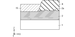
- FIG. 17 is a plan view of the SiC-SBD. As shown in FIG. 17, a surface electrode 2 is formed in the central current-carrying region, and a protective insulating film 4 is formed around it to ensure insulation from the surroundings. The difference from the case shown in FIG. 1 is that a surface electrode 15 is formed covering a part of the upper surface of the surface electrode 2.
- FIG. 18 is a sectional view corresponding to the A-A' section indicated by the broken line in FIG. 17.
- a power semiconductor device of the front-back conduction type current flows in the Z-axis direction in FIG. 18.
- a surface electrode 15 is formed compared to the configuration shown in FIG. 2, it is possible to connect wiring to the outside using solder on the upper surface side of the power semiconductor device, and it is possible to conduct a large current. is also available.
- FIG. 19 is an enlarged view of the area surrounded by the broken line in FIG. 18.
- a surface electrode 2 is formed on the upper surface of the semiconductor substrate 1 , and a protective insulating film 4 and a surface electrode 15 are further formed on the upper surface of the surface electrode 2 .
- the arithmetic mean roughness of the upper surface of the protective insulating film 4 is smaller than the arithmetic mean roughness of the interface between the protective insulating film 4 and the surface electrode 2.
- a plurality of vertices are provided at the upper end of the protective insulating film 4.
- the interface between the surface electrode 2 and the surface electrode 15 is located below the interface between the surface electrode 2 and the protective insulating film 4.
- FIG. 20 is a flowchart illustrating an example of the SiC-SBD manufacturing process according to this embodiment. Further, FIGS. 5 to 12 are cross-sectional views showing examples of the manufacturing process of the SiC-SBD according to this embodiment. Hereinafter, the manufacturing process of the SiC-SBD will be specifically explained with reference to FIGS. 5 to 12.
- Steps ST01 to ST06 in FIG. 20 are the same as steps ST01 to ST06 in FIG. 4, so the explanation will be omitted.
- FIG. 21 is a cross-sectional view showing an example of the structure of a semiconductor device in which steps up to step ST06 in FIG. 20 have been completed.
- electrodes are formed on the surface of the semiconductor device using a plating method (corresponding to steps ST07 and ST08 in FIG. 20). Even if the plating treatment is performed on the Al or Al alloy electrode on the wafer after the generally known degreasing and pickling, the Al or Al alloy on the wafer (hereinafter, Al or Al alloy is also referred to as Al alloy) ) Since strong organic residues and oxide films are formed on the surface of the aluminum alloy, metal diffusion does not occur between the Al alloy and the plating metal, making it impossible to form a plating layer with strong adhesion. .
- the plating treatment for the Al alloy electrode on the wafer is performed in the order of plasma cleaning, degreasing, pickling, zincate treatment, and plating. Note that it is necessary to ensure sufficient water washing time between each step so that the treatment liquid or residue from the previous step is not brought into the next step.
- FIG. 22 is a flowchart showing an example of plating pretreatment and plating treatment.
- a surface activation treatment is performed as a plating pretreatment using, for example, plasma (corresponding to step ST11 in FIG. 22).
- plasma cleaning using plasma uses plasma to oxidize or decompose or knock out organic residues that are baked onto the Al alloy electrode and cannot be removed by general plating pretreatment. This process cleans the surface of the Al alloy electrode.
- degreasing treatment and acid cleaning are performed as plating pretreatment (corresponding to step ST12 and step ST13 in FIG. 22).
- the degreasing process is a process performed to remove slight organic contamination or oxide film remaining on the surface of the Al alloy.
- acid cleaning is a process that neutralizes the surface of the Al alloy, and further etch the surface of the Al alloy to make the surface rough, increasing the reactivity of the treatment solution in the subsequent process, and improving the adhesion of plating. .
- step ST14 zincate treatment is performed as a plating pretreatment (corresponding to step ST14 in FIG. 22).
- a plating process is performed to form a plating film with strong adhesion.
- electroless Ni plating is performed, electroless Au plating is performed (corresponding to step ST15 and step ST16 in FIG. 22).
- the zincate treatment is a treatment for forming a zinc (Zn) film on the surface of an Al alloy while removing an oxide film of Al.
- Zn zinc
- the standard redox potential of Zn is nobler than that of Al, so that Al is dissolved as ions.
- the Zn ions receive electrons on the surface of the Al alloy due to the electrons generated at this time, and form a Zn film on the surface of the Al. Further, at this time, the Al oxide film is also removed.
- FIGS. 23 and 24 are flowcharts showing modified examples of zincate processing.
- step ST21 in FIG. 23 first, surface activation treatment such as plasma cleaning is performed (corresponding to step ST21 in FIG. 23). Next, degreasing treatment and acid cleaning are performed (corresponding to steps ST22 and ST23 in FIG. 23).
- a first zincate process is performed (corresponding to step ST24 in FIG. 23). Then, after performing zincate peeling (corresponding to step ST25 in FIG. 23), the second zincate treatment is performed again (corresponding to step ST26 in FIG. 23).
- a plating film with strong adhesion is formed by performing a plating process. Specifically, after electroless Ni plating is performed, electroless Au plating is performed (corresponding to step ST27 and step ST28 in FIG. 23).
- step ST31 in FIG. 24 surface activation treatment such as plasma cleaning is performed (corresponding to step ST31 in FIG. 24).
- degreasing treatment and acid cleaning are performed (corresponding to steps ST32 and ST33 in FIG. 24).
- a first zincate process is performed (corresponding to step ST34 in FIG. 24). Then, after performing zincate peeling (corresponding to step ST35 in FIG. 24), the second zincate treatment is performed again (corresponding to step ST36 in FIG. 24). Further, after performing zincate peeling (corresponding to step ST37 in FIG. 24), a third zincate treatment is performed again (corresponding to step ST38 in FIG. 24).
- a plating film with strong adhesion is formed by performing a plating process. Specifically, after electroless Ni plating is performed, electroless Au plating is performed (corresponding to step ST39 and step ST40 in FIG. 24).
- the Zn-coated Al alloy is immersed in concentrated nitric acid, the Zn is dissolved, and a thin, uniform layer is formed on the Al surface. An Al oxide film is formed. Then, the Al alloy is immersed in the Zn treatment solution again, so that the surface of the Al alloy is coated with Zn, and the oxide film of Al is removed.
- the oxide film layer on the surface of the Al alloy becomes thinner and smoother.
- the more the above operations are performed the more uniform the Al surface becomes, and the quality of the plating film is improved.
- the zincate treatment shown in FIG. It is desirable to carry out the zincate treatment three times.
- the interface between the surface electrode 2 and the surface electrode 15 is made smaller than the interface between the surface electrode 2 and the protective insulating film 4.
- an interface can be formed such that it is located below. Note that when forming such a lower interface, a surface activation treatment (corresponding to step ST11) shown in FIG. 22 can also be used.
- FIG. 25, FIG. 26, FIG. 27, and FIG. 28 are diagrams showing examples of structures of semiconductor devices manufactured by the above-described flow. Further, FIG. 27 is an enlarged view of the area surrounded by the broken line in FIG. 26. In FIG. 27, the interface between the protective insulating film 4 and the surface electrode 2 is used as a reference plane, and the distance to the interface between the surface electrode 15 and the surface electrode 2 located below the reference plane is defined as d. do.
- the inventors have developed a semiconductor module in which the upper and lower surfaces of the semiconductor device 10 are joined to a lead frame 12 via the solder 11, and further sealed with a mold resin 14, as shown in FIG. An assembly test was conducted.
- the soldering process is repeated three times as an accelerated test, so that more stress is applied to the protective insulating film 4 from the surface electrode 2, the surface electrode 15, the solder 11, or the lead frame 12. situation.
- FIG. 29 is a diagram showing the relationship between the difference between the interface between the surface electrode 2 and the surface electrode 15 and the interface between the surface electrode 2 and the protective insulating film 4 and the defective rate after the assembly test.
- the vertical axis shows the defective rate of the semiconductor module after the assembly test
- the horizontal axis shows the difference [nm] between the interface between the surface electrode 2 and the surface electrode 15 and the interface between the surface electrode 2 and the protective insulating film 4.
- the portion where the horizontal axis is negative indicates that the interface between the surface electrode 2 and the surface electrode 15 protrudes with respect to the interface between the surface electrode 2 and the protective insulating film 4. There is.
- the defect rate of the semiconductor module after the assembly test can be reduced. Can be suppressed.
- ⁇ Third embodiment> A power conversion device and a method for manufacturing the power conversion device according to the present embodiment will be described.
- components similar to those described in the embodiment described above will be illustrated with the same reference numerals, and detailed description thereof will be omitted as appropriate. .
- the semiconductor device according to the first embodiment and the second embodiment is applied to a power conversion device.
- the power conversion device according to this embodiment is not limited to a specific power conversion device, a case where the power conversion device according to this embodiment is applied to a three-phase inverter will be described below.
- FIG. 30 is a diagram schematically showing the configuration of a power conversion system to which the power conversion device 200 according to the present embodiment is applied.
- the power conversion system shown in FIG. 30 includes a power supply 100, a power conversion device 200, and a load 300.
- the power supply 100 is a DC power supply and supplies DC power to the power conversion device 200.
- the power source 100 can be configured with various power sources, for example, it may be configured with a DC system, a solar battery, a storage battery, or a rectifier circuit or an AC/DC converter connected to an AC system. good.
- the power supply 100 may be configured by a DC/DC converter that converts DC power output from a DC system into predetermined power.
- the power conversion device 200 is a three-phase inverter connected between the power source 100 and the load 300.
- Power converter 200 converts DC power supplied from power supply 100 into AC power and supplies it to load 300.
- Power conversion device 200 includes a main conversion circuit 201 and a control circuit 203.
- the main conversion circuit 201 converts input DC power into AC power and outputs the AC power.
- Control circuit 203 outputs a control signal for controlling main conversion circuit 201 to main conversion circuit 201 .
- the load 300 is a three-phase electric motor driven by AC power supplied from the power converter 200.
- the load 300 is not limited to a specific application, but is a motor installed in various electrical devices, and is used, for example, as a motor for a hybrid vehicle, an electric vehicle, a railway vehicle, an elevator, or an air conditioner.
- the main conversion circuit 201 includes a switching element and a free wheel diode (not shown here). By switching the switching element, the main conversion circuit 201 converts the DC power supplied from the power supply 100 into AC power, and supplies it to the load 300.
- the main conversion circuit 201 is a two-level three-phase full bridge circuit, and has six switching elements and each switching element. It can be constructed from six freewheeling diodes arranged in antiparallel.
- the semiconductor device 202 according to the first embodiment, the second embodiment, or any of their modifications is applied to at least one of the switching element and the free-wheeling diode of the main conversion circuit 201.
- the six switching elements are connected in series every two switching elements to form an upper and lower arm, and each upper and lower arm forms a respective phase (U phase, V phase, W phase) of the full bridge circuit.
- the output terminals of the respective upper and lower arms, that is, the three output terminals of the main conversion circuit 201 are connected to the load 300.
- the main conversion circuit 201 includes a drive circuit (not shown) that drives each switching element.
- the drive circuit generates a drive signal for driving the switching element of the main conversion circuit 201 and supplies it to the control electrode of the switching element of the main conversion circuit 201.
- the drive circuit controls each switching element using a drive signal that turns on the switching element and a drive signal that turns the switching element off in accordance with a control signal from a control circuit 203 that will be described later. Output to electrode.
- the drive signal is a voltage signal (on signal) that is higher than the threshold voltage of the switching element
- the drive signal is the threshold voltage of the switching element. This is a voltage signal (off signal) below the voltage.
- the control circuit 203 controls the switching elements of the main conversion circuit 201 so that the desired power is supplied to the load 300. Specifically, the control circuit 203 calculates the time (on time) during which each switching element of the main conversion circuit 201 should be in the on state, based on the power to be supplied to the load 300. For example, the control circuit 203 can control the main conversion circuit 201 by pulse width modulation (PWM) control that modulates the on-time of the switching element according to the voltage to be output. The control circuit 203 then outputs an on signal to the switching element that should be in the on state and an off signal to the switching element that should be in the off state at each time point. A control command (control signal) is output to the drive circuit included in the main conversion circuit 201. The drive circuit outputs an on signal or an off signal as a drive signal to the control electrode of each switching element in accordance with this control signal.
- PWM pulse width modulation
- the method for manufacturing power conversion device 200 includes the following steps.
- the semiconductor device 202 is manufactured by the manufacturing method described in the first embodiment, the second embodiment, or a modification thereof.
- a main conversion circuit 201 having this semiconductor device 202 is formed.
- a control circuit 203 is also formed.
- a power conversion device 200 is thus formed.
- the main conversion circuit 201 is formed, for example, as shown in FIG. It is joined to the lead frame 12.
- the semiconductor device 202 according to the first embodiment or the second embodiment is used as at least one of the semiconductor devices 202 configuring the main conversion circuit 201.
- This makes it possible to suppress defects caused by stress from peripheral members when the semiconductor device 202 is in operation and in non-operation.
- This increases the reliability of the main conversion circuit 201. Therefore, the reliability of power conversion device 200 can be improved.
- the semiconductor device 202 is applied to a two-level three-phase inverter
- this embodiment is not limited to this, and can be applied to various power conversion devices. be able to.
- the power conversion device is a two-level power conversion device, but it may be a multi-level power conversion device such as a three-level power conversion device.
- the power conversion device described above may be applied to a single-phase inverter.
- the power conversion device is not limited to the case where the above-mentioned load is an electric motor, but is applicable to any one of, for example, an electric discharge machine, a laser processing machine, an induction heating cooker, and a non-contact device power supply system. It can also be used as a power supply device, and furthermore, it can be used as a power conditioner for a solar power generation system or a power storage system.
- ⁇ About the configuration of the semiconductor device> 1 2, and 31 are diagrams schematically showing examples of the configuration of a semiconductor device manufactured by the manufacturing method described in this embodiment.
- a SiC-Schottky barrier diode (SBD) is shown.
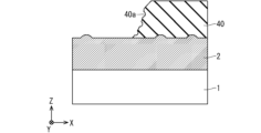
- FIG. 31 is a cross-sectional view corresponding to the area surrounded by the broken line in FIG. 2. The difference from the case shown in FIG. 3 is that a recess 40a is provided in the side surface portion of the protective insulating film 40.
- a surface electrode 2 is formed on the upper surface of the semiconductor substrate 1, and a protective insulating film 40 is further formed on the upper surface of the surface electrode 2.
- the arithmetic mean roughness of the top surface of the protective insulating film 40 is smaller than the arithmetic mean roughness of the side surfaces of the protective insulating film 40 .
- the arithmetic mean roughness of the side surface of the protective insulating film 40 is smaller than the arithmetic mean roughness of the interface between the protective insulating film 40 and the surface electrode 2 (that is, the lower surface of the protective insulating film 40).
- a plurality of vertices are provided at the upper end of the protective insulating film 40.
- FIG. 4 is a flowchart illustrating an example of the SiC-SBD manufacturing process according to this embodiment.
- the corresponding cross-sectional views from FIG. 5 to FIG. 9 up to the formation of the surface electrode (step ST03) are the same as those in the first embodiment, and therefore the description thereof will be omitted.
- a protective insulating film 4 (protective insulating film 40 in this embodiment) is formed.
- the material for the protective insulating film is preferably polyimide or silicone resin, and these materials can be applied to the uppermost surface of the SiC-SBD by using spin coating, photolithography, etching, or inkjet coating technology.
- a protective insulating film is formed on the outer periphery (corresponding to step ST04 in FIG. 4).
- Protective insulating film 4 covers a portion of the upper surface of drift layer 7 that is not covered by surface electrode 2 . Further, the protective insulating film covers a part of the upper surface of the front electrode 2 .
- a plurality of vertices are formed on the upper surface of the protective insulating film 40 by performing surface treatment with plasma containing oxygen and argon using, for example, a batch-type plasma processing apparatus.
- a recess 40 a is formed on the side surface of the protective insulating film 40 .
- the reliability is further improved by forming a plurality of vertices on the upper surface of the protective insulating film 40 on the outer peripheral side of the semiconductor device and unevenness (concavities 40a) on the side surfaces of the protective insulating film 40.
- the arithmetic mean roughness of the top surface of the protective insulating film 40 is smaller than the arithmetic mean roughness of the side surfaces of the protective insulating film 40;
- the roughness is smaller than the arithmetic mean roughness of the interface between the protective insulating film 40 and the surface electrode 2 (that is, the lower surface of the protective insulating film 40). Therefore, with respect to the stress that the protective insulating film 40 receives from the mold resin 14, the external force applied between the protective insulating film 40 and the surface electrode 2 can be alleviated compared to the first embodiment. Peeling of the insulating film 40 can be suppressed.
- FIG. 32, and FIG. 33 are diagrams schematically showing an example of the structure of a semiconductor device manufactured by the manufacturing method described in this embodiment.
- a SiC-Schottky barrier diode (SBD) is shown.
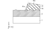
- FIG. 32 is a cross-sectional view corresponding to the area surrounded by the broken line in FIG. 33. The difference from the case shown in FIG. 3 is that an inclined portion 41b is provided on the upper surface of the protective insulating film 41.
- FIG. 4 is a flowchart illustrating an example of the SiC-SBD manufacturing process according to this embodiment.
- the corresponding cross-sectional views from FIG. 5 to FIG. 9 up to the formation of the surface electrode (step ST03) are the same as those in the first embodiment, and therefore the description thereof will be omitted.
- a protective insulating film 4 (protective insulating film 41 in this embodiment) is formed.
- the material for the protective insulating film is preferably polyimide or silicone resin, and these materials can be applied to the uppermost surface of the SiC-SBD by using spin coating, photolithography, etching, or inkjet coating technology.
- a protective insulating film is formed on the outer periphery (corresponding to step ST04 in FIG. 4).
- Protective insulating film 4 (protective insulating film 41 in this embodiment) covers a portion of the upper surface of drift layer 7 that is not covered by surface electrode 2 . Further, the protective insulating film covers a part of the upper surface of the front electrode 2 .
- a plurality of vertices are formed on the upper surface of the protective insulating film 41 by performing surface treatment with plasma containing oxygen and argon using, for example, a batch type plasma processing apparatus. At this time, if a plurality of vertices are also formed on the upper surface of the protective insulating film 41 on the outer peripheral side of the semiconductor device, reliability is further improved.
- the upper surface of the protective insulating film 41 is changed to a surface parallel to the semiconductor substrate (that is, the upper surface of the protective insulating film 41 is
- An inclined portion 41b having an angle of ⁇ 3 (that is, inclined) with respect to the upper surface of the substrate may be provided.
- FIGS. 1, 32, and 33 Obtain a semiconductor device that can be used.
- the edge of the protective insulating film 41 deforms in response to the stress that the semiconductor device receives from the molding resin 14. Can absorb stress. Therefore, cracks occurring in the protective insulating film 41 can be suppressed.
- the replacement may be performed across multiple embodiments. That is, the respective configurations shown as examples in different embodiments may be combined to produce similar effects.
- the semiconductor device includes a semiconductor layer, a first electrode layer, and an insulating film.
- the semiconductor layer corresponds to, for example, the drift layer 6 or the drift layer 7.
- the first electrode layer corresponds to, for example, the surface electrode 2.
- the insulating film corresponds to, for example, the protective insulating film 4.
- the surface electrode 2 covers a part of the upper surface of the drift layer 7 via the drift layer 6, the Schottky electrode layer 9, and the like.
- the protective insulating film 4 covers another part of the upper surface of the drift layer 7 via the drift layer 6, the Schottky electrode layer 9, and the like.
- the protective insulating film 4 covers a part of the upper surface of the front electrode 2 .
- the arithmetic mean roughness of the upper surface of the protective insulating film 4 is smaller than the arithmetic mean roughness of the interface between the protective insulating film 4 and the surface electrode 2.
- the contact area of the protective insulating film 4 with the upper component is smaller than the contact area of the protective insulating film 4 with the lower component. Therefore, the connection with the components below the protective insulating film 4 can be made stronger than the connection with the components above the protective insulating film 4. Peeling can be suppressed. According to such a configuration, the reliability of the semiconductor device can be improved.
- the end of the upper surface of the protective insulating film 4 is an inclined surface. Both the apex formed at the upper end of the inclined surface and the apex formed at the lower end of the inclined surface are obtuse angles. According to such a configuration, by having a plurality of vertices at the upper and lower ends of the inclined surface, stress applied to the protective insulating film 4 from the surroundings can be dispersed. Further, by setting the angle of each vertex to 90 degrees or more, it is possible to reduce the force applied to the vertex, thereby suppressing the occurrence of cracks in the protective insulating film 4.
- the semiconductor device includes a second electrode layer that covers a portion of the surface electrode 2.
- the second electrode layer corresponds to, for example, the surface electrode 15.
- the protective insulating film 4 covers a part of the surface electrode 2. Further, the interface between the surface electrode 15 and the surface electrode 2 is located below the interface between the protective insulating film 4 and the surface electrode 2. According to such a configuration, the force that the protective insulating film 4 receives from the surface electrode 15 can be reduced. Therefore, peeling of the protective insulating film 4 can be suppressed.
- the ridge line 4a on the side surface of the protective insulating film 4 has a concave shape. According to such a configuration, generation of cracks in the protective insulating film 4 can be suppressed.
- the main conversion circuit 201 includes the above-described semiconductor device and converts and outputs input power, and the control for controlling the main conversion circuit 201
- the control circuit 203 outputs a signal to the main conversion circuit 201.
- the contact area of the protective insulating film 4 with the upper component is smaller than the contact area of the protective insulating film 4 with the lower component. Therefore, the connection with the components below the protective insulating film 4 can be made stronger than the connection with the components above the protective insulating film 4. Peeling can be suppressed. According to such a configuration, the reliability of the power conversion device including the semiconductor device can be improved.
- the surface electrode 2 is formed to cover a part of the upper surface of the drift layer 6.
- a protective insulating film 4 is formed to cover another part of the upper surface of the drift layer 6 and at least a part of the upper surface of the surface electrode 2.
- the arithmetic mean roughness of the upper surface of the protective insulating film 4 is smaller than the arithmetic mean roughness of the interface between the protective insulating film 4 and the surface electrode 2.
- the contact area of the protective insulating film 4 with the upper component is smaller than the contact area of the protective insulating film 4 with the lower component. Therefore, the connection with the components below the protective insulating film 4 can be made stronger than the connection with the components above the protective insulating film 4. Peeling can be suppressed. According to such a configuration, the reliability of the semiconductor device can be improved.
- the main converter includes a semiconductor device manufactured by the above manufacturing method, and converts and outputs input power.
- a circuit 201 is provided.
- a control circuit 203 that outputs a control signal for controlling the main conversion circuit 201 to the main conversion circuit 201 is provided.
- the contact area of the protective insulating film 4 with the upper component is smaller than the contact area of the protective insulating film 4 with the lower component. Therefore, the connection with the components below the protective insulating film 4 can be made stronger than the connection with the components above the protective insulating film 4. Peeling can be suppressed.
- the material may contain other additives, such as This includes alloys, etc.
- each component in the embodiments described above is a conceptual unit, and within the scope of the technology disclosed in this specification, a case where one component consists of a plurality of structures This includes a case where one component corresponds to a part of a certain structure, and a case where a plurality of components are included in one structure.
- each component in the embodiments described above includes structures having other structures or shapes as long as they exhibit the same function.
- a semiconductor layer (Additional note 1) a semiconductor layer; a first electrode layer covering a part of the upper surface of the semiconductor layer; an insulating film that covers another part of the upper surface of the semiconductor layer and a part of the upper surface of the first electrode layer,
- the arithmetic mean roughness of the upper surface of the insulating film is smaller than the arithmetic mean roughness of the interface between the insulating film and the first electrode layer.
- An end of the upper surface of the insulating film is an inclined surface
- the apex formed at the upper end of the inclined surface and the apex formed at the lower end of the inclined surface are both obtuse angles, Semiconductor equipment.
- the insulating film covers a part of the first electrode layer, further comprising a second electrode layer covering a portion of the first electrode layer, an interface between the second electrode layer and the first electrode layer is located below an interface between the insulating film and the first electrode layer; Semiconductor equipment.
- a main conversion circuit that includes the semiconductor device according to any one of Supplementary Notes 1 to 4 and that converts and outputs input power; a control circuit that outputs a control signal for controlling the main conversion circuit to the main conversion circuit; Power converter.
- (Appendix 7) a semiconductor layer; a first electrode layer covering a part of the upper surface of the semiconductor layer; an insulating film covering another part of the upper surface of the semiconductor layer and a part of the upper surface of the first electrode layer,
- the arithmetic mean roughness of the upper surface of the insulating film is smaller than the arithmetic mean roughness of the side surface of the insulating film,
- the arithmetic mean roughness of the side surface of the insulating film is smaller than the arithmetic mean roughness of the interface between the insulating film and the first electrode layer.
- (Appendix 8) a semiconductor layer; a first electrode layer covering a part of the upper surface of the semiconductor layer; an insulating film that covers another part of the upper surface of the semiconductor layer and a part of the upper surface of the first electrode layer,
- the arithmetic mean roughness of the upper surface of the insulating film is smaller than the arithmetic mean roughness of the side surface of the insulating film,
- the arithmetic mean roughness of the side surface of the insulating film is smaller than the arithmetic mean roughness of the interface between the insulating film and the first electrode layer.
Landscapes
- Electrodes Of Semiconductors (AREA)
Priority Applications (4)
| Application Number | Priority Date | Filing Date | Title |
|---|---|---|---|
| JP2024528425A JP7789208B2 (ja) | 2022-06-22 | 2023-05-22 | 半導体装置、電力変換装置、および、半導体装置の製造方法 |
| DE112023002719.6T DE112023002719T5 (de) | 2022-06-22 | 2023-05-22 | Halbleiterbauteil, Stromwandlervorrichtung und Verfahren zum Herstellen des Halbleiterbauteils |
| US18/859,403 US20250273527A1 (en) | 2022-06-22 | 2023-05-22 | Semiconductor device, power conversion apparatus, and method of manufacturing semiconductor device |
| CN202380047145.4A CN119384877A (zh) | 2022-06-22 | 2023-05-22 | 半导体装置、电力转换装置以及半导体装置的制造方法 |
Applications Claiming Priority (2)
| Application Number | Priority Date | Filing Date | Title |
|---|---|---|---|
| JP2022-100048 | 2022-06-22 | ||
| JP2022100048 | 2022-06-22 |
Publications (1)
| Publication Number | Publication Date |
|---|---|
| WO2023248670A1 true WO2023248670A1 (ja) | 2023-12-28 |
Family
ID=89379721
Family Applications (1)
| Application Number | Title | Priority Date | Filing Date |
|---|---|---|---|
| PCT/JP2023/018941 Ceased WO2023248670A1 (ja) | 2022-06-22 | 2023-05-22 | 半導体装置、電力変換装置、および、半導体装置の製造方法 |
Country Status (5)
| Country | Link |
|---|---|
| US (1) | US20250273527A1 (https=) |
| JP (1) | JP7789208B2 (https=) |
| CN (1) | CN119384877A (https=) |
| DE (1) | DE112023002719T5 (https=) |
| WO (1) | WO2023248670A1 (https=) |
Citations (4)
| Publication number | Priority date | Publication date | Assignee | Title |
|---|---|---|---|---|
| JP2004048639A (ja) * | 2002-05-17 | 2004-02-12 | Murata Mfg Co Ltd | 圧電共振子及びその製造方法等 |
| JP2006351943A (ja) * | 2005-06-17 | 2006-12-28 | Toppan Printing Co Ltd | マイクロ反応チップおよびその製造方法 |
| JP2018117026A (ja) * | 2017-01-17 | 2018-07-26 | 富士電機株式会社 | 半導体装置および半導体装置の製造方法 |
| WO2021033664A1 (ja) * | 2019-08-21 | 2021-02-25 | 株式会社村田製作所 | 半導体装置 |
-
2023
- 2023-05-22 JP JP2024528425A patent/JP7789208B2/ja active Active
- 2023-05-22 WO PCT/JP2023/018941 patent/WO2023248670A1/ja not_active Ceased
- 2023-05-22 US US18/859,403 patent/US20250273527A1/en active Pending
- 2023-05-22 CN CN202380047145.4A patent/CN119384877A/zh active Pending
- 2023-05-22 DE DE112023002719.6T patent/DE112023002719T5/de active Pending
Patent Citations (4)
| Publication number | Priority date | Publication date | Assignee | Title |
|---|---|---|---|---|
| JP2004048639A (ja) * | 2002-05-17 | 2004-02-12 | Murata Mfg Co Ltd | 圧電共振子及びその製造方法等 |
| JP2006351943A (ja) * | 2005-06-17 | 2006-12-28 | Toppan Printing Co Ltd | マイクロ反応チップおよびその製造方法 |
| JP2018117026A (ja) * | 2017-01-17 | 2018-07-26 | 富士電機株式会社 | 半導体装置および半導体装置の製造方法 |
| WO2021033664A1 (ja) * | 2019-08-21 | 2021-02-25 | 株式会社村田製作所 | 半導体装置 |
Also Published As
| Publication number | Publication date |
|---|---|
| US20250273527A1 (en) | 2025-08-28 |
| CN119384877A (zh) | 2025-01-28 |
| JPWO2023248670A1 (https=) | 2023-12-28 |
| DE112023002719T5 (de) | 2025-04-17 |
| JP7789208B2 (ja) | 2025-12-19 |
Similar Documents
| Publication | Publication Date | Title |
|---|---|---|
| JP7109650B2 (ja) | 電力用半導体装置および電力変換装置 | |
| JP6987213B2 (ja) | 半導体装置、電力変換装置 | |
| JP7229428B2 (ja) | 電力用半導体装置、電力用半導体装置の製造方法および電力変換装置 | |
| JP7584620B2 (ja) | 半導体素子の製造方法 | |
| CN109860159B (zh) | 半导体模块、其制造方法以及电力变换装置 | |
| JP7386662B2 (ja) | 半導体装置および電力変換装置 | |
| US20250254967A1 (en) | Silicon carbide semiconductor device, power converter, and method for manufacturing silicon carbide semiconductor device | |
| WO2023248670A1 (ja) | 半導体装置、電力変換装置、および、半導体装置の製造方法 | |
| JP6892023B1 (ja) | 半導体装置、半導体装置の製造方法および電力変換装置 | |
| JPWO2019171523A1 (ja) | 半導体素子、半導体装置、電力変換装置、及び、半導体素子の製造方法 | |
| JP2022054004A (ja) | 半導体装置の製造方法、半導体装置および電力変換装置 | |
| US20250113533A1 (en) | Semiconductor device and power conversion device | |
| JP2023178555A (ja) | 半導体装置および電力変換装置 | |
| WO2024214501A1 (ja) | 半導体装置及び電力変換装置 | |
| WO2024248086A1 (ja) | 半導体素子、半導体装置、電力変換装置、および半導体素子の製造方法 | |
| JP2023158319A (ja) | 半導体装置および電力変換装置 | |
| JP2024172182A (ja) | 半導体装置、電力変換装置、半導体装置の製造装置、半導体装置の製造方法、および、電力変換装置の製造方法 | |
| JP2025008136A (ja) | 半導体装置、半導体装置の製造方法、及び、電力変換装置 | |
| WO2024214634A1 (ja) | 半導体装置及び電力変換装置 | |
| JP2024123834A (ja) | 炭化珪素半導体装置及び電力変換装置 | |
| JP2023117734A (ja) | 半導体装置の製造方法、半導体装置、および電力変換装置 | |
| WO2021240748A1 (ja) | 半導体装置およびその製造方法ならびに電力変換装置 |
Legal Events
| Date | Code | Title | Description |
|---|---|---|---|
| 121 | Ep: the epo has been informed by wipo that ep was designated in this application |
Ref document number: 23826858 Country of ref document: EP Kind code of ref document: A1 |
|
| WWE | Wipo information: entry into national phase |
Ref document number: 2024528425 Country of ref document: JP |
|
| WWE | Wipo information: entry into national phase |
Ref document number: 18859403 Country of ref document: US |
|
| WWE | Wipo information: entry into national phase |
Ref document number: 202380047145.4 Country of ref document: CN |
|
| WWE | Wipo information: entry into national phase |
Ref document number: 112023002719 Country of ref document: DE |
|
| WWP | Wipo information: published in national office |
Ref document number: 202380047145.4 Country of ref document: CN |
|
| WWP | Wipo information: published in national office |
Ref document number: 112023002719 Country of ref document: DE |
|
| 122 | Ep: pct application non-entry in european phase |
Ref document number: 23826858 Country of ref document: EP Kind code of ref document: A1 |
|
| WWP | Wipo information: published in national office |
Ref document number: 18859403 Country of ref document: US |