WO2023238480A1 - 光学ラインセンサ - Google Patents
光学ラインセンサ Download PDFInfo
- Publication number
- WO2023238480A1 WO2023238480A1 PCT/JP2023/012244 JP2023012244W WO2023238480A1 WO 2023238480 A1 WO2023238480 A1 WO 2023238480A1 JP 2023012244 W JP2023012244 W JP 2023012244W WO 2023238480 A1 WO2023238480 A1 WO 2023238480A1
- Authority
- WO
- WIPO (PCT)
- Prior art keywords
- light
- light receiving
- lens
- scanning direction
- receiving element
- Prior art date
Links
- 230000003287 optical effect Effects 0.000 title claims abstract description 147
- 238000003491 array Methods 0.000 claims description 49
- 238000007689 inspection Methods 0.000 claims description 36
- 238000009826 distribution Methods 0.000 claims description 32
- 238000005286 illumination Methods 0.000 claims description 17
- 239000011521 glass Substances 0.000 claims description 6
- 238000003672 processing method Methods 0.000 claims description 6
- 239000011347 resin Substances 0.000 claims description 3
- 229920005989 resin Polymers 0.000 claims description 3
- 230000000149 penetrating effect Effects 0.000 claims 1
- 238000010586 diagram Methods 0.000 description 23
- 238000000034 method Methods 0.000 description 23
- 230000004075 alteration Effects 0.000 description 19
- 230000004048 modification Effects 0.000 description 11
- 238000012986 modification Methods 0.000 description 11
- 238000004519 manufacturing process Methods 0.000 description 6
- 230000008569 process Effects 0.000 description 6
- 230000007423 decrease Effects 0.000 description 5
- 230000009467 reduction Effects 0.000 description 4
- 239000004065 semiconductor Substances 0.000 description 4
- 230000008901 benefit Effects 0.000 description 3
- 230000015572 biosynthetic process Effects 0.000 description 3
- 230000008859 change Effects 0.000 description 3
- 230000000052 comparative effect Effects 0.000 description 3
- 230000007547 defect Effects 0.000 description 3
- 230000009022 nonlinear effect Effects 0.000 description 3
- 239000007787 solid Substances 0.000 description 3
- 238000003786 synthesis reaction Methods 0.000 description 3
- 238000003705 background correction Methods 0.000 description 2
- 230000000903 blocking effect Effects 0.000 description 2
- 230000006866 deterioration Effects 0.000 description 2
- 238000005192 partition Methods 0.000 description 2
- 230000001681 protective effect Effects 0.000 description 2
- 239000000758 substrate Substances 0.000 description 2
- 230000001629 suppression Effects 0.000 description 2
- 206010010071 Coma Diseases 0.000 description 1
- 238000009825 accumulation Methods 0.000 description 1
- 201000009310 astigmatism Diseases 0.000 description 1
- 235000013361 beverage Nutrition 0.000 description 1
- 239000003086 colorant Substances 0.000 description 1
- 239000013065 commercial product Substances 0.000 description 1
- 238000005336 cracking Methods 0.000 description 1
- 238000009792 diffusion process Methods 0.000 description 1
- 230000000694 effects Effects 0.000 description 1
- 230000007613 environmental effect Effects 0.000 description 1
- 238000002073 fluorescence micrograph Methods 0.000 description 1
- 239000000463 material Substances 0.000 description 1
- 238000000465 moulding Methods 0.000 description 1
- 230000000704 physical effect Effects 0.000 description 1
- 239000000047 product Substances 0.000 description 1
- 230000001902 propagating effect Effects 0.000 description 1
- 239000013589 supplement Substances 0.000 description 1
- 230000002194 synthesizing effect Effects 0.000 description 1
Images


Classifications
-
- G—PHYSICS
- G01—MEASURING; TESTING
- G01N—INVESTIGATING OR ANALYSING MATERIALS BY DETERMINING THEIR CHEMICAL OR PHYSICAL PROPERTIES
- G01N21/00—Investigating or analysing materials by the use of optical means, i.e. using sub-millimetre waves, infrared, visible or ultraviolet light
- G01N21/84—Systems specially adapted for particular applications
- G01N21/88—Investigating the presence of flaws or contamination
- G01N21/89—Investigating the presence of flaws or contamination in moving material, e.g. running paper or textiles
- G01N21/892—Investigating the presence of flaws or contamination in moving material, e.g. running paper or textiles characterised by the flaw, defect or object feature examined
-
- H—ELECTRICITY
- H04—ELECTRIC COMMUNICATION TECHNIQUE
- H04N—PICTORIAL COMMUNICATION, e.g. TELEVISION
- H04N1/00—Scanning, transmission or reproduction of documents or the like, e.g. facsimile transmission; Details thereof
- H04N1/024—Details of scanning heads ; Means for illuminating the original
- H04N1/028—Details of scanning heads ; Means for illuminating the original for picture information pick-up
-
- H—ELECTRICITY
- H04—ELECTRIC COMMUNICATION TECHNIQUE
- H04N—PICTORIAL COMMUNICATION, e.g. TELEVISION
- H04N1/00—Scanning, transmission or reproduction of documents or the like, e.g. facsimile transmission; Details thereof
- H04N1/04—Scanning arrangements, i.e. arrangements for the displacement of active reading or reproducing elements relative to the original or reproducing medium, or vice versa
- H04N1/047—Detection, control or error compensation of scanning velocity or position
- H04N1/053—Detection, control or error compensation of scanning velocity or position in main scanning direction, e.g. synchronisation of line start or picture elements in a line
-
- H—ELECTRICITY
- H04—ELECTRIC COMMUNICATION TECHNIQUE
- H04N—PICTORIAL COMMUNICATION, e.g. TELEVISION
- H04N1/00—Scanning, transmission or reproduction of documents or the like, e.g. facsimile transmission; Details thereof
- H04N1/04—Scanning arrangements, i.e. arrangements for the displacement of active reading or reproducing elements relative to the original or reproducing medium, or vice versa
- H04N1/19—Scanning arrangements, i.e. arrangements for the displacement of active reading or reproducing elements relative to the original or reproducing medium, or vice versa using multi-element arrays
Definitions
- the present invention mainly relates to an optical line sensor that detects scratches and defects on the surface of thin inspection objects such as printed matter and films, and scratches and defects inside transparent films.
- CIS Contact type optical sensors
- CIS Contact type optical sensors
- surface inspection machines have been considered for inspection purposes such as surface inspection in the manufacturing process of thin and wide film products, and inspection of labels affixed to various beverage containers, food containers, cans, etc. Some of them have been commercialized.
- W.D. working distance
- SELFOC SELFOC
- SELFOC a registered trademark, the same shall apply hereinafter
- W.D. D. A long CIS is desired.
- the depth of field was usable even if it was relatively shallow, but in the manufacturing process of the inspection object, there was a large variation in the optical axis direction of the inspection object. For this reason, CIS with a deep depth of field is also highly desired.
- a typical CIS with a deep depth of field is a telecentric optical system using a mirror optical system, as shown in Patent Documents 1 to 5.
- the optical system is very complex. It is extremely difficult to manufacture this optical system and use it as a commercial product. That is, during manufacturing, the process becomes complicated, and problems arise in terms of manufacturing stability and increased costs. Furthermore, even after it is commercialized, the optical axis may become misaligned due to environmental changes or changes over time due to the complex optical system, which tends to cause performance deterioration compared to conventional CIS with a simple structure. The problem remains.
- Patent Document 6 a refractive lens made of glass or resin was used, and W. D. It is possible to improve the depth of field.
- Patent Document 7 a certain number of solutions have been proposed as shown in Patent Document 6 and Patent Document 7.
- Patent Document 6 one telecentric refractive optical system is arranged at a distance between line sensors arranged in a staggered manner, and lenses serving as the refractive optical system are arranged at a distance to form an array, thereby increasing the depth of field.
- Patent Document 7 a method of preventing crosstalk between lenses by providing a partition plate between lenses separated from each other is studied.
- Patent Document 6 and Patent Document 7 it is possible to improve the depth of field and prevent crosstalk between lenses, but the normal telecentric refractive optical system is large and difficult to make compact. . Further, in the partition plate shown in Patent Document 7, missing pixels occur during reading, resulting in incomplete reading. Furthermore, there is no solution to the shading that occurs in principle with one lens when the lenses are spaced apart. There is also no mention of a method for suppressing so-called ripples in the reading line direction. Moreover, the refractive optical system described above has not even been realized to date.
- inspection machines that use camera lenses, such as line cameras, which are different from the above-mentioned method are large and require a large number of inspection machines in order to handle wide inspection objects at manufacturing sites. Therefore, the entire device becomes very large and its cost is enormous, making it difficult to deploy it in each process of a factory.
- the illumination system uses a new refractive lens with a long time and deep depth of field, and a new method to suppress ripples, which are optical unevenness on the light receiving sensor caused by shading of individual lenses.
- Optical line sensors are desired.
- the present invention aims to realize a compact optical line sensor with a deep depth of field.
- the optical line sensor according to the present invention is an optical line sensor that reads an inspection object conveyed in the sub-scanning direction with a reading line extending in the main-scanning direction, and includes a plurality of light-receiving lenses and a plurality of light-receiving elements. There is.
- the plurality of light receiving lenses are arranged along the main scanning direction.
- the plurality of light receiving elements are arranged in a line along the main scanning direction, and receive light transmitted through the plurality of light receiving lenses.
- the plurality of light receiving elements form at least two or more rows of the reading lines.
- the light receiving lens constitutes a telecentric optical system, and the width in the sub-scanning direction is smaller than the width in the main scanning direction.
- the present invention by using a telecentric optical system, it is possible to realize an optical line sensor with a deep depth of field. Furthermore, since the width of the light receiving lens in the sub-scanning direction is smaller than the width in the main scanning direction, the light receiving lens can be arranged closer to the sub-scanning direction, and as a result, the optical line sensor can be made more compact. If the light-receiving lens is placed closer to the sub-scanning direction, the light-receiving element can also be placed closer to the sub-scanning direction. This makes it possible to simplify the synthesis process.
- FIG. 2 is a cross-sectional view of a typical CIS.
- FIG. 2 is an exploded perspective view of a line-shaped illumination optical system for CIS.
- FIG. 7 is a schematic diagram of a light receiving system in which the fields of view of each light receiving lens do not overlap when each light receiving lens is arranged to act as a monocular lens.
- FIG. 7 is a schematic diagram showing another example of a light receiving system in which a plurality of light receiving element arrays are arranged.
- FIG. 7 is a schematic diagram showing still another example of a light receiving system in which a plurality of light receiving element arrays are arranged.
- N for each wavelength.
- A. It is a graph showing the relationship between and the diffraction limit.
- FIG. 2 is a schematic diagram showing an example of an arrangement method when using an RGB-LED or an RGB-LD (laser diode; semiconductor laser) as a light source.
- FIG. 3 is a side view showing a specific example of an arrangement method when an LD is used as a light source.
- FIG. 2 is a schematic diagram showing the positional relationship between a light source and a light-receiving lens, in a case where the light-receiving element array is arranged in two rows.
- FIG. 7 is a schematic diagram showing a modification of the light receiving system.
- FIG. 7 is a schematic diagram showing a modification of the light receiving system.
- FIG. 7 is a schematic diagram showing a modification of the light receiving system.
- FIG. 7 is a schematic diagram showing a modification of the light receiving system.
- FIG. 7 is a schematic diagram showing a modification of the light receiving system.
- FIG. 7 is a schematic diagram showing a modification of the light receiving system.
- FIG. 7 is a schematic diagram showing a modification of the light receiving system.
- FIG. 7 is a schematic diagram showing a modification of the light receiving system.
- FIG. 7 is a schematic diagram showing a modification of the light receiving system.
- FIG. 7 is a schematic diagram showing a modification of the light receiving system.
- FIG. 3 is a schematic diagram for explaining the position of the optical axis in the light receiving system.
- FIG. 3 is a schematic diagram for explaining the position of the optical axis in the light receiving system.
- FIG. 7 is a diagram showing the light intensity distribution on the light receiving surface of the light receiving element array when the light intensity distribution of the light source is flat when the end portion of the lens is a parallelogram.
- FIG. 6 is a diagram showing details of a light intensity distribution near a connecting portion between adjacent light-receiving lenses. In the example of FIG. 12E, the light intensity of the light receiving area is shown, and the reason why no signal dropout portion occurs is schematically illustrated.
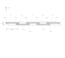
- FIG. 1 shows a cross-sectional view near the longitudinal center of the CIS.
- FIG. 2 is an exploded perspective view.
- the X direction is the main scanning direction
- the Y direction is the sub scanning direction.
- the Z direction is perpendicular to the X direction and the Y direction.
- the linear light source section 10 is an illumination optical system that has an elongated light amount distribution in the main scanning direction.
- two housings 16 are arranged facing each other with a focal plane (inspection plane) 20 in between.
- a linear light source 10 is provided inside each housing 16 to illuminate the object to be inspected on the focal plane 20 .
- a light-receiving lens 11 and a light-receiving section 12 are provided in one of the casings 16, and light from the illuminated inspection object is guided to the light-receiving section 12 by the light-receiving lens 11.
- the light-receiving lens 11 forms an image of light from the object to be inspected on the light-receiving section 12 .
- one of the two light source sections 10 is disposed on the light receiving section 12 side, and the other is disposed on the opposite side from the light receiving section 12 side, with respect to the focal plane 20.
- the light receiving section 12 is mounted on a substrate 13 fixed to one housing 16.
- the light that has passed through the light-receiving lens 11 is received by the light-receiving surface 12A of the light-receiving section 12, and a signal corresponding to the amount of received light is output from the light-receiving section 12.
- a signal corresponding to the amount of received light is output from the light-receiving section 12.
- the inspection object conveyed in the sub-scanning direction (Y direction) is read by the light receiving section 12 extending in the main scanning direction (X direction) at the reading line formed by the light receiving surface 12A of the light receiving section 12. It will be done.
- the light B3 emitted from one light source section 10 passes through the protective glass 14 fixed to the housing 16, and then passes through the reflective member 17A provided on the inner surface of the protective glass 14A fixed to the other housing 16. and is guided to the focal plane 20.
- An ultraviolet light blocking filter (UV cut filter) 15 that blocks ultraviolet light from entering the light receiving section 12 is provided at an arbitrary position from the focal plane 20 to the light receiving section 12 .
- a color filter 18 is provided between the light receiving section 12 and the ultraviolet light blocking filter 15, which allows visible light in a specific wavelength range to pass through.
- a substrate 5 for fixing a light source 103 (an ultraviolet light source, a visible light source, etc.) provided in the light source section 10 is installed at a position facing the bottom surface of the light source section 10 in one of the casings 16.
- the light source unit 10 includes a transparent light guide 101 extending along the longitudinal direction L, a light source 103 provided near one end surface in the longitudinal direction L, and a light guide 101. and a cover member 102 for holding each side of the.
- the light emitted from the light source 103 enters the light guide 101, is appropriately reflected by the light diffusion pattern P while propagating through the light guide 101, and is emitted from the light exit surface in the direction of the arrow, forming a line of illumination light.
- the object to be inspected is illuminated.
- the depth of field of such CIS is shallow, and if the object to be inspected is thick, it is difficult to inspect the entire thickness direction. D. Because the area is narrow, it often comes into contact with the object to be inspected and the inspection itself is not successful.
- a SELFOC (manufactured by Nippon Sheet Glass Co., Ltd.) lens array is used as the light receiving lens 11, for example.
- the SELFOC lens array is an erect, equal-magnification lens array.
- cylindrical SELFOC lenses are stacked in bales to form a multi-lens lens.
- the advantage of a multi-lens lens is that it is possible to make the so-called brightness of the lens brighter than that of a single lens. That is, the F-number when a plurality of single lenses are arranged to form a multi-lens lens is smaller than the F-number of a single lens.
- CIS as described above are disadvantageous in terms of depth of field and depth of focus.
- the larger the numerical aperture the shallower the depth of field.
- the magnification is large, ie N. A.
- the depth of field becomes shallower as the image size increases.
- the aperture is adjusted to ensure the depth of field. That is, N. A. to obtain the desired depth of field.
- the optical axes of each lens are different and intersect, so compared to monocular lenses, the image tends to blur when the object to be inspected changes in the direction of the optical axis. It has become.
- the above is a major drawback of the stacked multi-lens SELFOC lens array. Therefore, as a result of studying how it is possible to deepen the depth of field of a compact optical line sensor, an example obtained is described below.
- the light receiving lens 11 constitutes a telecentric optical system.
- the first method is to create an array structure that can be considered as a monocular lens of the optical line sensor, as shown in FIG.
- FIG. 3 is a schematic diagram of a light receiving system in which the fields of view of the light receiving lenses 11 do not overlap.
- each light receiving lens 11 is arranged apart in the main scanning direction (X direction) so that the field of view of each light receiving lens 11 does not overlap, and each light receiving lens 11 is also arranged in the sub scanning direction (Y direction). By spacing them apart, the light receiving lenses 11 are arranged in a staggered manner.
- a plurality of light receiving lenses 11 arranged along the main scanning direction (X direction) are arranged apart from each other.
- a plurality of light receiving lenses 11 arranged along the main scanning direction (X direction) are integrally held by a lens holder 110.
- a light receiving element array is formed by arranging a plurality of light receiving elements (not shown) in a line along the main scanning direction (X direction). 120 are arranged. That is, one light receiving element array 120 is configured by arranging a plurality of light receiving elements in an array along the main scanning direction (X direction). Each light receiving element receives the light transmitted through each light receiving lens 11.
- a light receiving element array 120 is arranged in association with each light receiving lens 11.
- the light receiving element arrays 120 made up of short sensors are alternately arranged in a staggered manner along the main scanning direction (X direction).
- a plurality of light receiving element arrays 120 arranged along the main scanning direction (X direction) form one read line L, and in the example of FIG. 3, two read lines L are formed.
- the lens holder 110 is not limited to a configuration in which it is provided in correspondence with each reading line L, but may also be configured such that a plurality of light receiving lenses 11 corresponding to each reading line L are integrally held in one lens holder. good.
- a plurality of light receiving lenses 11 may be arranged in a number corresponding to the plurality of light receiving element arrays 120.
- the optical axis of the light transmitted through each light-receiving lens 11 and guided to each light-receiving element array 120 may pass through approximately the center in the main scanning direction (X direction) of each light-receiving element array 120 in one-to-one correspondence.
- a plurality of light receiving element arrays 120 are arranged in a plurality of rows in the sub-scanning direction (Y direction). That is, a plurality of rows of light receiving element arrays 120 are arranged spaced apart in a direction (Y direction) perpendicular to the arrangement direction (X direction) of the light receiving elements.
- Each light receiving lens 11 has a width W1 in the sub-scanning direction that is smaller than a width W2 (lens diameter) in the main scanning direction. That is, each light receiving lens 11 has an elongated shape along the main scanning direction.
- the width W1 of each light-receiving lens 11 in the sub-scanning direction corresponds to the field of view of each light-receiving lens 11 in the sub-scanning direction.
- the width W2 of each light receiving lens 11 in the main scanning direction corresponds to the field of view of each light receiving lens 11 in the main scanning direction.
- Each light receiving lens 11 has an N. A. is 0.001 ⁇ N. A. It is preferable that the width W1 in the sub-scanning direction is set so as to satisfy ⁇ 0.05.
- each light receiving lens 11 has the same shape, and is formed into a rectangular shape when viewed from a direction (Z direction) perpendicular to the main scanning direction and the sub scanning direction.
- each light-receiving lens 11 is not limited to a rectangle (rectangle), but may be oval or elliptical, or may have another shape.
- the plurality of light-receiving lenses 11 are spaced apart from each other by a width W2 or less in the main scanning direction of the light-receiving lenses. In other words, it is preferable that the plurality of light receiving lenses 11 be spaced apart from each other by less than or equal to the field of view dimension (within the field of view) of the light receiving lenses 11 in the main scanning direction. As in the example of FIG. 3, the fields of view of the respective light receiving lenses 11 may be overlapped in the sub-scanning direction. In this case, the pixel outputs from the light receiving elements in the portion where the fields of view of the plurality of light receiving lenses 11 overlap may be subtracted.
- the image of one light-receiving lens 11 (the amount of light transmitted through one light-receiving lens 11) is excluded from the data output from the light-receiving element, or the pixels from the light-receiving element are The output may be reduced to approximately half the output value.
- a plurality of light-receiving element arrays (light-receiving element array 120), occurrence of pixel loss can be more reliably prevented than in the case of one line of light-receiving element arrays.
- FIG. 4 is a schematic diagram showing another example of a light receiving system in which a plurality of light receiving element arrays 120 are arranged.
- each light-receiving lens 11 and each light-receiving element array 120 do not correspond one-to-one, but a plurality of (two in this example) light-receiving lenses 11 arranged in the main scanning direction form one light-receiving element array. It corresponds to 120.
- a plurality of light receiving lenses 11 corresponding to one light receiving element array 120 are adjacent to each other in the main scanning direction. However, the plurality of light receiving lenses 11 corresponding to one light receiving element array 120 may be spaced apart from each other, and in this case, may be spaced apart from each other by a width W2 or less of the light receiving lenses 11 in the main scanning direction. Further, a light shielding member may be provided between each light receiving lens 11.
- FIG. 5 is a schematic diagram showing still another example of a light receiving system in which a plurality of light receiving element arrays 120 are arranged.
- a plurality (in this example, two) of light receiving element arrays 120 each consisting of long sensors of the same length (length corresponding to the total length in the main scanning direction) are arranged in parallel in the sub scanning direction.
- a plurality of light receiving element arrays 120 may be arranged as many as .
- the short photodetector arrays 120 may be used in a staggered arrangement (see FIGS. 3 and 4), or two rows of photodetector arrays 120 may be arranged spaced apart ( (See FIG. 5), but the present invention is not limited to this, and more light receiving element arrays 120 may be arranged spaced apart in the sub-scanning direction (Y direction).
- the conventional CIS is N. A. is large, so it was possible to ignore the blurring of the image due to the diffraction limit.
- W. D. In order to increase N., it is necessary to increase the focal length of the light receiving lens. A. Therefore, with a conventional lens diameter, as the focal length increases, the influence of diffraction increases accordingly. In this embodiment, by increasing the lens diameter, W. D. We propose a method that does not degrade the optical resolution even when the image blur due to the diffraction limit is reduced by increasing the length of the image.
- Figure 6 shows the N. A. represents the relationship between and the diffraction limit. In the light-receiving lens 11 having the same lens parameters, if the so-called pitch of the light-receiving lens 11 itself is shortened, the focal length will be increased and the influence of aberrations will be reduced.
- FIG. 7A shows the relationship between the effective diameter of SELFOC lens A and the diameter of the circle of confusion
- FIG. 7B shows the relationship between the effective diameter of SELFOC lens A and the diameter of the circle of confusion.
- FIG. 7C shows the relationship between the effective diameter and the diameter of the circle of confusion of the SELFOC lens C, respectively.
- the solid line shows the total circle of confusion
- the broken line shows the circle of confusion due to diffraction
- the dashed-dotted line shows the geometric-optical circle of confusion.
- the relationship between the circle of least confusion and the diffraction limit, that is, the optical resolution at a certain lens diameter and focal length can be seen. Therefore, in the case of the light-receiving lens 11 shown in FIG. 7A, it can be seen that as the effective diameter ⁇ becomes larger, the diameter of the circle of confusion becomes smaller, and it is sufficient that the effective diameter ⁇ is 1.0 mm ⁇ 3.0 mm.
- the light receiving lens 11 shown in FIG. 7A is a SELFOC lens having smaller aberrations and a larger effective diameter than the light receiving lens 11 shown in FIG. 7B, and it can be seen that the light receiving lens 11 shown in FIG. 7A should be selected. Furthermore, the light-receiving lens 11 of FIG. 7A, which has the same focal length, has a lower N. A.
- the light receiving lens 11 shown in FIG. 7A is preferable from the viewpoint of noise suppression. Furthermore, if the same amount of noise is allowed, it can be said that the light receiving lens 11 of FIG. 7A can improve the scanning speed nine times as compared to the light receiving lens 11 of FIG. 7B.
- SELFOC lens C has little aberration and can have a large effective diameter.
- the parameters of SELFOC lenses A to C shown in FIGS. 7A to 7C are shown in Table 1 below.
- the most important parameter shown in Table 1 is the refractive index distribution constant.
- the light-receiving lens 11 with fewer aberrations when the effective diameter is enlarged and the focal length is extended is the SELFOC lens A, which has the smallest refractive index distribution constant, and the light-receiving lens 11 with the second smallest aberration is the SELFOC lens C.
- FIG. 8A shows the relationship between the effective diameter of rod lens A and the diameter of the circle of confusion
- FIG. 8B shows the relationship between the effective diameter of rod lens B.
- FIG. 8C shows the relationship between the effective diameter of the rod lens C and the diameter of the circle of confusion
- FIG. 8D shows the relationship between the effective diameter of the rod lens D and the diameter of the circle of confusion.
- the solid line represents the total circle of confusion
- the broken line represents the circle of confusion due to diffraction
- the dashed line represents the geometric optical circle of confusion.
- the parameters of the rod lenses A to D shown in FIGS. 8A to 8D are shown in Table 2 below. It can be seen that plastic rod lenses have the same tendency as SELFOC lenses. Considering the refractive index of the plastic rod lens and the refractive index of the glass lens, the axial refractive index is preferably about 1.45 to about 1.65.
- the refractive index distribution constant is the dominant factor in aberrations.
- the more gradually the refractive index changes the less aberrations will occur.
- a rapid angle change means an increase in higher-order nonlinear effects when polynomial expansion of Snell'Law is performed.
- the deviation from paraxial optics increases, resulting in increased aberrations.
- the inventor of the present application has determined that the focal length or W. D.
- the light receiving lens 11 in the present invention is not limited to a gradient index lens such as a SELFOC lens or a plastic rod lens, but can also be used with other lenses, such as achromat (achromatic), apochromat, etc., considering cost.
- a lens with equal aberrations due to nonlinear effects in the above gradient index lens that is, a lens with equal spherical aberration, coma aberration, and astigmatism, or a telecentric refractive optical system in the above gradient index lens.
- a gradient index lens such as a SELFOC lens or a plastic rod lens, which has the same aberration due to nonlinear effects and the same diffraction limit, and has the same arrangement and dimensions (aperture). This also applies to the light receiving lens 11 that forms an inverted image, which will be described later.
- the optical system described above is centered on an erect lens, it may be an inverted optical system if the fields of view do not overlap. That is, the configuration may be such that the plurality of light receiving lenses 11 form an inverted image. If it is a two-row type lens array, it is also possible to employ an inverted optical system. In the case of an inverted optical system, since the image is inverted symmetrical about the optical axis, it is sufficient to convert the inverted image into an erect image by image processing when synthesizing the images. That is, the image synthesis process may be performed after inverting the inverted images of the plurality of light receiving lenses 11 and converting them into erect images.
- an inverted refractive optical system in signal processing for each light receiving element, for example, data obtained from one of two rows of light receiving element arrays arranged in a staggered manner so as to be spaced apart in the sub-scanning direction is acquired over a long period of time.
- the data obtained from the other light-receiving element array may be acquired for a short period of time, the acquired image may be inverted into an erect image, and then the images may be combined.
- the overlapping portions may be multiplied or subtracted by a correction coefficient when combining the images.
- the plurality of light receiving element arrays may be shorter than each of the plurality of reading lines arranged in two rows of reading lines. Further, the light receiving element array arranged in one reading line and the light receiving element array arranged in the other reading line may be arranged alternately in a staggered manner along the main scanning direction. Such a configuration is the same as that of the erecting type refractive optical system described in FIG. 3, so a detailed explanation will be omitted.
- the plurality of light receiving elements constitute a plurality of light receiving element arrays 120 by arranging them in an array of two or more rows. Further, each of the plurality of light receiving element arrays 120 is spaced apart from each other by a width W2 or less in the main scanning direction of the light receiving lens 11 in a direction perpendicular to the reading line L.
- the plurality of light-receiving lenses 11 are arranged in a number corresponding to the plurality of light-receiving element arrays 120, and the optical axis of the light transmitted through each light-receiving lens 11 and guided to each light-receiving element array 120 is an abbreviation of each light-receiving element array 120. Penetrates through the center.
- optical axis of the light transmitted through each light-receiving lens 11 and guided to each light-receiving element array 120 may pass through a position apart from the approximate center of each light-receiving element array 120 in parallel to the sub-scanning direction.
- the light source 103 W. D. Since the length is more than 10 times longer than that of conventional CIS, the inspection surface illuminance needs to be more than 100 times longer in the same magnification system. Therefore, as the light source 103, for example, a high-intensity white LED array is used. In other words, the plurality of light sources 103 may include white LEDs.
- the emitted beam is expanded in the main scanning direction and collimated in the sub-scanning direction to reduce unevenness in the amount of light during irradiation.
- FIG. 9A An example of an arrangement method when using an RGB-LED or an RGB-LD (laser diode; semiconductor laser) as the light source 103 is shown in FIG. 9A.
- the plurality of light sources 103 may include a red LED (R), a green LED (G), and a blue LED (B), or may include a laser diode.
- a plurality of light sources 103 are mounted on a light source board 134, and a heat sink 135 is attached to the light source board 134.
- the beams emitted from each light source 103 are collimated by an ellipsoidal condenser lens 104 having different lens powers in the main scanning direction and the sub-scanning direction, and are irradiated onto the object to be inspected.
- an ellipsoidal condenser lens 104 having different lens powers in the main scanning direction and the sub-scanning direction, and are irradiated onto the object to be inspected.
- the ellipsoidal condensing lens 104 is shown here, any lens may be used as long as it has different lens powers in the main scanning direction and the sub-scanning direction. Note that the power of a lens is the reciprocal of the focal length, and is a measure of the refractive power of the lens.
- FIG. 9B is a side view showing a specific example of an arrangement method when an LD is used as the light source 103.
- the LD with the larger divergence angle is arranged parallel to the main scanning direction.
- the beams emitted from the red LD 131, green LD 132, and blue LD 133 that constitute the light source 103 are collimated by the condensing lenses 104 associated with each beam, and then focused onto the inspection surface by the cylindrical lens 105.
- each of the RGB colors is irradiated at substantially the same position in the sub-scanning direction, making it possible to reduce color unevenness in the sub-scanning direction.
- a light source 103 such as an LED or LD and diffusely reflected on the inspection surface is imaged on a light receiving element array by a light receiving lens system.
- the light receiving element uses an element size of 62 ⁇ m corresponding to 400 dpi to 42 ⁇ m corresponding to 600 dpi.
- the power of the illumination light may be increased accordingly.
- the plurality of light sources 103 include a plurality of light sources 131 to 133 having different wavelengths, and the light sources 131 to 133 are taken as one unit, and a plurality of one unit of light sources 103 are arranged in the main scanning direction (X direction).
- the configuration may be
- the amount of light received decreases approximately in inverse proportion to the square of the area of the light-receiving element. do.
- determine the amount of illumination light As the element size becomes smaller, the amount of received light decreases in inverse proportion to the element area for the same accumulation time. This is a physical property of semiconductor photodetectors, and in order to maintain the S/N ratio, it is necessary to increase the illumination light, increase the power density, and make the number of generated electrons generated per unit time the same. .
- the light received by the light receiving element depends not only on the illuminance of the inspection surface but also on the range that the light receiving element sees when receiving the light. Needless to say, the solid angle of light reception is different, and as the angle decreases, the amount of light received also decreases, and if the inspection surface is a completely diffusing surface, the amount of light received will be in accordance with the so-called cos ⁇ law.
- the light diffusely reflected from the inspection surface is captured by the light receiving lens and focused on the light receiving element, and the output signal is output from the light receiving element.
- the output signals from the light-receiving element array are branched from serial to parallel to improve processing speed and transmitted to the image processing device.
- FIG. 10A is a schematic diagram showing the positional relationship between the light source 103 and the light-receiving lens 11, in the case where the light-receiving element array 120 is arranged in two rows.
- FIG. 10A shows the arrangement of the light source 103 with respect to the light receiving lenses 11 and the light receiving element array 120 arranged in two rows.
- the light source 103 is arranged approximately at the center of the two reading lines L.
- Each light source 103 is arranged parallel to the reading line L.
- the optical axis of each light source 103 intersects with the optical axis of the light that passes through each light receiving lens 11 and is guided to each light receiving element array 120, and also passes through each light receiving lens 11 and is guided to each light receiving element array 120.
- the light source 103 irradiates the inspection surface with light at an angle of about 45 degrees. Therefore, the W. D. Considering this, the distance between the light source 103 and the inspection surface was set to 70 mm. In this embodiment, an LD is used, but an LED of each wavelength may be used.
- the arrangement pitch of the light sources 103 is adjusted to the distance between the lenses, and the light sources 103 are arranged at a position that is approximately at the center between the adjacent light-receiving lenses 11 and at the same time approximately at the center of the two rows of reading lines L. By doing so, it is possible to further prevent missing pixels on the inspection surface, and at the same time, it is possible to further reduce shading of the light receiving lens 11 and unevenness in the amount of light from the light source 103.
- the lens pitch between the light receiving lenses 11 in each row was 7 mm. In this case, the substantial lens pitch is 3.5 mm.
- FIG. 10B is a diagram showing the relationship between the light amount distribution of the light source 103 (on the inspection surface), the light amount distribution on the light receiving element surface, and the shading of the light receiving lens 11 in the main scanning direction.
- the light amount distribution on the light receiving element array 120 becomes flat as schematically shown in FIG. 10B, and it becomes possible to effectively use the dynamic range of the light receiving elements.
- an illumination system is used to irradiate the object to be inspected with illumination light having a negative intensity distribution.
- a method of arranging the light source 103 between adjacent light-receiving lenses 11 does not provide a shading suppression method that is completely compatible with various types of light-receiving lenses 11 . That is, each light-receiving lens 11 has its own unique shading, and if the light-receiving lenses 11 are different, an illumination optical system must be used accordingly.
- a condensing lens 104 having a large power in the main scanning direction is arranged.
- the light beam transmitted through the condenser lens 104 is then guided to the object to be inspected by a converging lens such as a cylindrical lens 105, and forms a light intensity on the object to be inspected according to the shading of the light receiving lens 11.
- a converging lens such as a cylindrical lens 105
- the light intensity on the light receiving element is Distribution can be smoothed.
- the condensing lens 104 may have power in the sub-scanning direction.
- the condensing lens 104 is, for example, a cylindrical lens, a lenticular lens, a Fresnel lens, or a combination of a prism sheet and a spherical lens.
- the light source 103 may be placed at an intermediate position between the light receiving lenses 11 or may be placed on the optical axis of the light receiving lenses 11. Furthermore, the light source 103 may be placed at a position on the outer periphery of the light receiving lens 11. Furthermore, it is more preferable that the lens has power distribution in the main scanning direction.
- a condensing lens 104 that condenses light beams from a plurality of light sources 103 is provided as a single lens body, and the power in the main scanning direction of the lens body is greater than the power in the sub-scanning direction. It's also big.
- the condenser lens 104 may include a first condenser lens and a second condenser lens instead of one lens body.
- the power of the first condenser lens in the main scanning direction may be greater than the power in the sub-scanning direction
- the power of the second condensing lens may be greater in the sub-scanning direction than the power in the main scanning direction.
- the power in the main scanning direction may be adjustable by the first condenser lens and the second condenser lens.
- the first condenser lens and the second condenser lens may be a cylindrical lens, a lenticular lens, a Fresnel lens, or a prism array. It can be configured as follows.
- the first condenser lens may be a lenticular lens or a prism array.
- the second condensing lens may be a Fresnel lens or a cylindrical lens.
- FIG. 10C shows a graph of MTF of the light receiving system according to lens diameter in this embodiment.
- the solid line, short broken line, long broken line, and dashed-dotted line show cases where the effective diameter ⁇ is 1.0, 1.5, 2.0, 2.5, and 3.0 mm in this order.
- the pixel dimensions of the light-receiving element are 42.3 ⁇ m in both the main scanning direction and the sub-scanning direction, corresponding to 600 dpi.
- the range if the performance is about 30% at 12 lines/mm equivalent to 600 dpi, the range from ⁇ 1.0 mm to ⁇ 3. It satisfies the MTF characteristics in the range up to 0mm.
- the comparative example does not satisfy the MTF characteristics in all ranges of the effective diameter ⁇ . This indicates that the aberration characteristics are better when ⁇ A is 0.077 than when ⁇ A is 0.154.
- the lens is preferably made of glass or resin.
- the axial refractive index N0 is 1.45 ⁇ N0 ⁇ 1.65
- the refractive index distribution constant ⁇ A is 0.05 ⁇ A ⁇ 0.12
- the focal point It is preferable that the distance f is 50 mm ⁇ f ⁇ 150 mm.
- the light-receiving lens 11 may be an achromat or apochromat, each of which is a combination of a plurality of lenses.
- the lens system may be a combination of only convex lenses as a plurality of lenses, or a lens system may be a combination of a convex lens and a concave lens as a plurality of lenses.
- the focal length f of the plurality of lenses satisfies 25 mm ⁇ f ⁇ 250 mm, and further preferably that the aperture diameter ⁇ of the plurality of lenses satisfies 2 mm ⁇ 50 mm.
- the light receiving lens system is a reduction optical system
- the configuration of the optical system is the same as that in FIG. 10A, and the magnification of the light receiving lens 11 is changed. That is, the relationship between the lateral magnification of the object point and the image point of the light receiving lens 11 is changed to 9:1 or 4:1.
- the depth of field is increased to three times that of a life-size system when the horizontal magnification is 9:1, and twice that of a life-size system when the horizontal magnification is 4:1.
- the size of the light receiving element is 1/9 the size of the same size light receiving element.
- the size of the light receiving element is set to 1/4 the size of the same size light receiving element. In this embodiment, a light receiving element of 1/4 the size is used to double the depth of field.
- the graph (solid line) in FIG. 11 shows the MTF characteristic during defocusing of the reduction optical system in this embodiment.
- the graph (broken line) in FIG. 11 shows the MTF characteristics of a 1-magnification system during defocusing. From the comparison of the reduced optical system and the 1x system in the figure, it can be seen that the depth of field of the reduced optical system is about twice as deep as that of the 1x system.
- the N. of the light receiving lens 11 is A. If the reduction ratio is S, then it increases by 1/S, which is its reciprocal. Therefore, even when the lens diameter of the light receiving lens 11 is small, if the reduction ratio is increased according to the focal length, the effective N. A. is maintained, so the blur caused by the diffraction effect can also be kept constant.
- the telecentric optical system By using a telecentric optical system, it is possible to create a configuration that is easy to assemble and has little change over time.
- the telecentric optical system is a double-sided telecentric optical system in which the light-receiving lens 11 is arranged on both the inspection object side and the light-receiving element array 120 side, or an object-side telecentric optical system in which the light-receiving lens 11 is arranged only on the inspection object side. It is an optical system.
- a beam of light that spreads narrowly from the object to be inspected parallel to the optical axis passes through the front lens, becoming a parallel beam of light, and the parallel beam of light that passes through an aperture inserted after the front lens passes through the rear lens.
- the light is then narrowed down to each light receiving element of the light receiving element array 120.
- N the shortest distance Ls of the staggered light receiving element array 120 in the sub-scanning direction is Ls>3 mm.
- the light receiving element array 120 can be It satisfies the angle and can be made compact, and at the same time, the memory capacity can be reduced.
- the N. of the light receiving lens 11 is A. is preferably about 0.001 to 0.05 from the viewpoint of the amount of illumination light.
- the thickness of the light-receiving lens 11 in the sub-scanning direction is determined by the N. A. Since it is determined by the solid angle defined by , it can be shortened in the sub-scanning direction, making it compact.
- FIGS. 12A to 12G Modifications of the light receiving system
- modifications of the light receiving system will be described using FIGS. 12A to 12G.
- a configuration in which a plurality of light receiving lenses 11 are arranged in two rows in the sub-scanning direction has been described, but in FIGS. 12A to 12G, a plurality of light receiving lenses 11 are arranged in one row in the main scanning direction.
- the light-receiving lens 11 When forming two lines of reading lines L by arranging the light-receiving element array 120 in a staggered manner, if the light-receiving lenses 11 are also arranged in two staggered lines in the same way as the light-receiving element array 120, the required N. A. In order to satisfy the following, it is necessary to provide an interval between the light receiving element arrays 120 in the sub-scanning direction that is greater than the width of the light-receiving lens 11 in the sub-scanning direction. Therefore, as shown in FIGS. 12A to 12G, the light-receiving lens 11 is provided with the necessary N. A.
- the plurality of light receiving lenses 11 each have the same shape when viewed from a direction perpendicular to the main scanning direction. Specifically, each light receiving lens 11 has the same shape when viewed from the Z direction perpendicular to the main scanning direction (X direction) and the sub scanning direction (Y direction). Note that the "same shape” includes substantially the same shape, such as an inverted shape, and a slight difference in shape is included in the "same shape.”
- each light receiving lens 11 has a parallelogram shape when viewed in the Z direction. That is, both end surfaces of each light-receiving lens 11 in the main scanning direction are inclined with respect to the sub-scanning direction. The inclination angles of both end faces of each light receiving lens 11 in the main scanning direction are the same.
- a plurality of light-receiving lenses 11 are arranged side by side in the main scanning direction as shown in FIG. 11 are arranged with their ends connected to each other.
- FIG. 12B rectangular notches are formed on both end surfaces in the main scanning direction of each light receiving lens 11 when viewed in the Z direction.
- a plurality of light-receiving lenses 11 are arranged side by side in the main scanning direction as shown in FIG. 12B, parts of adjacent light-receiving lenses 11 are fitted into notches formed on both end surfaces of each light-receiving lens 11. The ends of the light receiving lenses 11 adjacent to each other in the main scanning direction are connected to each other.
- each light receiving lens 11 has a trapezoidal shape when viewed in the Z direction. That is, both end surfaces of each light-receiving lens 11 in the main scanning direction are inclined with respect to the sub-scanning direction.
- the shape of each light receiving lens 11 when viewed in the Z direction is an inverted shape with respect to the main scanning direction with respect to the shape of the light receiving lenses 11 adjacent to each other in the main scanning direction when viewed in the Z direction.
- a plurality of light-receiving lenses 11 are arranged side by side in the main scanning direction as shown in FIG. 11 are arranged with their ends connected to each other. Thereby, the plurality of light-receiving lenses 11 are arranged in a state where adjacent light-receiving lenses 11 are inverted and connected.
- FIG. 12D curved (semicircular or semielliptical) notches are formed on both end surfaces in the main scanning direction of each light receiving lens 11 when viewed in the Z direction.
- a plurality of light-receiving lenses 11 are arranged side by side in the main scanning direction as shown in FIG. 12D, parts of adjacent light-receiving lenses 11 are fitted into notches formed on both end surfaces of each light-receiving lens 11.
- the ends of the light receiving lenses 11 adjacent to each other in the main scanning direction are connected to each other.
- FIG. 12E is a modification of FIG. 12C, and it is possible to prevent missing pixels from occurring in the above-mentioned light receiving element array 120 as much as possible.
- each light-receiving element array 120 is arranged on the longer side side of the widthwise center of each trapezoidal light-receiving lens 11. Further, the length of each light receiving element array 120 in the main scanning direction substantially matches the length of each of the trapezoidal light receiving lenses 11 in the main scanning direction at the position where the light receiving element array 120 is arranged.
- the staggered light receiving element arrays 120 adjacent to each other in the portions indicated by the broken lines in FIG. 12E overlap in the main scanning direction, and as will be described later, the staggered light receiving element arrays 120 shown in FIG. 12C overlap. This eliminates the possibility of missing parts of the output signal.
- FIGS. 12F and 12G show a case where a plurality of light receiving lenses 11 having a rectangular cutout shape are inverted and connected
- FIG. 12G shows a case where a plurality of light receiving lenses 11 having a circular cutout shape are reversed and connected. In this manner, in FIGS. 12E to 12G, the plurality of light receiving lenses 11 are arranged with adjacent light receiving lenses 11 inverted and connected.
- the light-receiving lens 11 is linearly symmetrical in the sub-scanning direction, reversal connection is possible.
- FIGS. 12F and 12G similarly to the trapezoidal inverted connection shown in FIG. 12E, the broken line portions overlap, and as will be described later, no signal dropouts occur.
- the light receiving lens 11 in FIG. 12G includes an edge 112 to ensure rigidity and avoid cracking.
- the lens end has a cross-sectional shape such as a parallelogram, trapezoid, rectangle, or curved cutout (circle, ellipse).
- N of the light receiving lens system.
- A. By setting a width in the sub-scanning direction that satisfies the following and connecting them in one row, a lens array that extends in a straight line in the main scanning direction is formed. Furthermore, two rows of light receiving element arrays 120 arranged in a staggered manner are provided at the center of the lens array in the sub-scanning direction.
- the plurality of light receiving element arrays 120 are arranged at the center of each of the plurality of light receiving lenses 11 in the main scanning direction, and are arranged alternately in a staggered manner along the main scanning direction. By doing so, the light emitted from the object to be inspected can be delivered to two rows of staggered light receiving element arrays 120 using one row of lens arrays.
- a shielding portion 111 is provided between the ends of the light receiving lenses 11 adjacent in the main scanning direction.
- the shielding portion 111 is formed into a thin plate shape.
- the shielding portion 111 extends from between the ends of each light-receiving lens 11 toward the light-receiving element (light-receiving element array 120), and protrudes from the light-receiving lens 11 toward the object to be inspected.
- the shielding portion 111 has a width that is at least equal to or larger than the width W1 of the light receiving lens 11 in the sub-scanning direction.
- the shielding part 111 is omitted in FIGS. 12B to 12G, the shielding part 111 may be similarly provided between the ends of each light receiving lens 11.
- the shielding portion 111 is a thin crank-shaped shielding plate and a thin wave-shaped shielding plate, respectively. In short, it is sufficient to prevent light from leaking into adjacent light receiving systems at the connecting portion.
- a plurality of light sources 103 that illuminate the object to be inspected may be provided in one-to-one correspondence with the plurality of light receiving element arrays 120.
- the plurality of light sources 103 may each have an elongated shape extending in a straight line along the main scanning direction. In this case, as shown in FIGS. may be opposed in the Z direction. Thereby, the plurality of light sources 103 can be arranged in a staggered manner, and linear light can be efficiently incident on each light receiving element array 120.
- the plurality of light sources 103 have a plurality of lines of illumination light intensity distribution in the sub-scanning direction corresponding to the plurality of light receiving element arrays 120.
- a plurality of light sources 103 may be similarly provided in one-to-one correspondence with a plurality of light receiving element arrays 120.
- a light intensity distribution including two intensity peaks in the sub-scanning direction is created so that the light receiving element array 120 of each reading line L has a light intensity peak.
- Line illumination with since the spacing in the sub-scanning direction of the staggered light-receiving element array 120 is narrow, line illumination with one peak may be used.
- FIGS. 12H and 12I are schematic diagrams for explaining the position of the optical axis 113 in the light receiving system.
- the position of the optical axis 113 in the light receiving system will be explained using FIGS. 12H and 12I using the configuration of FIG. 12E as an example, but other configurations such as FIGS. , it is possible to similarly set the position of the optical axis 113.
- the optical axis 113 of the light transmitted through each light-receiving lens 11 and guided to each light-receiving element array 120 is at a position parallel to the sub-scanning direction (Y direction) from the approximate center of each light-receiving element array 120. Penetrate. Specifically, the optical axis 113 of each light-receiving lens 11 is approximately equidistant from each light-receiving element array 120 arranged in a staggered manner, and the optical axis 113 of each light-receiving element array 120 is arranged in a staggered manner in the main scanning direction. It penetrates at a position approximately 1/2 the length of. In this example, the optical axes 113 are arranged in a line along the main scanning direction (X direction), but the configuration is not limited to this.
- each optical axis 113 of the light transmitted through each light-receiving lens 11 and guided to each light-receiving element array 120 passes through approximately the center of each light-receiving element array 120 arranged in a staggered manner. Therefore, each optical axis 113 is arranged in a staggered manner along the two rows of reading lines L, similarly to each light receiving element array 120. In this way, by aligning the optical axis 113 of each light-receiving lens 11 with each light-receiving element array 120, aberrations can be reduced.
- FIG. 13 shows the light intensity distribution on the light receiving surface of the light receiving element array 120 when the light intensity distribution of the light source 103 is flat when the lens end is a parallelogram.
- FIG. 13 shows an example of the light intensity distribution on the light receiving surface of each light receiving element array 120 when the configuration of FIG. 12A is adopted.
- the lens array made up of a plurality of light receiving lenses 11 is assumed to be a lens array made up of three light receiving lenses 11 for convenience.
- FIG. 13 shows the light intensity on each light receiving element array 120 of the entire lens array, and the two figures on the right side show enlarged views.
- FIG. 14 shows details of the light intensity distribution near the connecting portion between adjacent light receiving lenses 11.
- a signal missing pixel in one photodetector array 120 is interpolated with a pixel in the other photodetector array 120.
- arrow marks indicate a method of interpolating signals of signal-missing pixels.
- a portion 121 surrounded by a broken line in FIG. 14 is a light-receiving element located at a connecting portion between adjacent light-receiving lenses 11, and a signal dropout portion occurs when light no longer reaches the light-receiving element. Therefore, in the present embodiment, in the adjacent photodetector arrays 120 arranged in a staggered manner, the output signal of the photodetector (portion 122 surrounded by a solid line) facing in the sub-scanning direction with respect to the photodetector in the portion 121 is used to detect the signal missing portion. Supplement the signal. In this way, a pixel interpolation section is formed along the sub-scanning direction at the connection section between adjacent light-receiving lenses 11 (see FIG. 13).
- the signal missing portion may be corrected in advance using a reference medium for inspection. A white chart for shading correction, a grid pattern, or the like can be used as the reference medium.
- the width of the light-receiving lens 11 in the sub-scanning direction in FIG. 13 is 5 mm. Therefore, when the light-receiving lenses 11 are arranged in two rows in a staggered manner, the minimum interval between the light-receiving element arrays 120 in the staggered arrangement must be 5 mm or more. However, when a single row of lens arrays is used as described above, the spacing becomes approximately 1/2 (just under 3.0 mm). Moreover, if shading correction is performed while taking into consideration the dynamic range of the light receiving element array 120, the spacing can be further narrowed.
- the interval in the sub-scanning direction of the staggered light receiving element array 120 is narrowed, and at the same time, it becomes possible to halve the number of light receiving lenses 11. Therefore, there are advantages in that it is less susceptible to fluctuations in the conveyance speed in the sub-scanning direction, and at the same time it can reduce costs.
- the lens system is a double-sided telecentric system. Of course, it goes without saying that an object-side telecentric system may also be used.
- one light receiving element for output signals from two light receiving elements separated in the sub-scanning direction at the same position in the main scanning direction, one light receiving element (portion 121 surrounded by a broken line) is processed.
- the output signal from the other light receiving element is lower than the output signal from the other light receiving element (part 122 surrounded by a solid line) and the output signal from one light receiving element is less than the threshold value, the output signal from the other light receiving element Interpolate.
- the output signal from the other light receiving element Interpolate.
- one row of output signals corresponding to the reading line L is generated. .
- the light receiving elements in the portion 123 surrounded by the two-dot chain line in FIG. 14 are opposed to each other in the sub-scanning direction, but are overlapped with each other by being shifted from the connecting portion of the adjacent light receiving lenses 11. Regarding such overlapping portions, there is no need for interpolation because no output signal is lost from the light receiving element.
- FIG. 15 shows the light intensity distribution at the end of the photodetector array 120 arranged in a staggered manner as in FIG. 14.
- the light-receiving elements in the portion 124 surrounded by the two-dot chain line in FIG. 15 are opposed to each other in the sub-scanning direction, but are overlapped with each other by being shifted from the connecting portions of the adjacent light-receiving lenses 11. As shown in FIG.
- one row of the light-receiving element array 120 arranged in a staggered manner eliminates the signal missing portion in the light-receiving part. It becomes possible to obtain the necessary signal for the read line L of the.
- one light receiving element is processed.
- one column of output signals corresponding to the reading line L is obtained.
- Light source part 11 Light receiving lens 12
- Light receiving part 20 Focal plane 103
- Light source 104 Condensing lens 105
- Cylindrical lens 110 Lens holder 111 Shielding part 120
- Light source board 135 Heat sink
Abstract
複数の受光レンズ11は、主走査方向に沿って複数配置されている。複数の受光素子は、主走査方向に沿ってライン状に配置され、複数の受光レンズ11を透過した光を受光する。複数の受光素子は少なくとも2列以上の読取ラインLを形成する。受光レンズ11は、テレセントリック光学系を構成しており、副走査方向における幅W1が主走査方向における幅W2よりも小さい。
Description
本願発明は、主として印刷物やフィルムなど薄い検査対象物の表面のキズ・欠陥及び透明フィルムの内部のキズ・欠陥を検出する光学ラインセンサに関するものである。
紙幣などの真贋を判別する検査機や、業務用複写機や、家庭用プリンタスキャナなどのフラットベットスキャナに用いられてきた密着型光学センサ(以下CISと記す)を、印刷物の印刷の出来のチェック、薄物・広幅のフィルム製品の製造工程における表面検査、各種の飲料容器や食品容器及び缶などに貼り付けたラベルの検査などを検査対象とした所謂面検機に応用することが検討されてきており、一部は製品化されている。
しかしながら、依然としてSELFOCレンズ(「SELFOC」は登録商標、以下同様)を応用したCISでは作動距離(以下W.D.と記す)が短く、工程で用いる場面では接触を回避するため、W.D.の長いCISが望まれている。加えて、紙幣等の紙葉類の検査では、被写界深度は比較的浅くとも使用に耐えられたが、前記検査対象物の製造工程では該検査対象物の光軸方向への変動が大きい理由からも被写界深度が深いCISも強く望まれている。
被写界深度の深いCISは、特許文献1~5に示されるようにミラー光学系を用いたテレセントリック光学系が代表的である。前記特許文献から、該光学系は非常に複雑であることが分かる。該光学系を製造し、商品として運用する際には、非常な困難を伴う。即ち、製造時には、工程が複雑化し、製造安定性やコストアップが問題となる。また、商品化された後にも、環境の変化や経時変化による複雑な光学系であるが故の光軸の狂いが発生し、従来の簡素な構造のCISに比べて性能の劣化を生じ易いなどの問題が残る。
そこで、前記テレセントリック反射光学系を用いず、ガラスや樹脂を用いた屈折系のレンズを用い、W.D.や被写界深度を向上させることが考えられる。前記の屈折系の光学系については、特許文献6及び特許文献7に示されるように一定程度の解決策が提案されている。例えば、特許文献6においては、千鳥配置したラインセンサに1個のテレセントリック屈折光学系を離間させて配置し、前記屈折光学系であるレンズを離間配置してアレイ化することにより、被写界深度の深い光学系を実現しようとしている。また、特許文献7においては、離間したレンズの間に仕切り板を設けることにより、レンズ間のクロストークを防止する方法について検討されている。前記の特許文献6及び特許文献7においては、被写界深度の向上並びにレンズ間のクロストークを防止することは出来るが、通常のテレセントリック屈折光学系は、大型であり、コンパクト化は困難である。また、特許文献7に示されている仕切り板では、読み取り時に欠落画素が発生し、読み取りが不完全となる。更に、レンズが離間することにより発生する1個のレンズが原理的に有するシェーディングの解決策については、示されていない。読取ライン方向の所謂リップルの抑制方法についても言及されていない。しかも、現在までに前記の屈折光学系方式は、実現されてもいない。
更に、前記方式と別方式であるラインカメラなどのカメラレンズを用いた検査機は、大型であり、製造現場の広幅の検査対象物に対応させるためには、多くの台数が必要である。そのため、装置全体が非常に大型になり、しかもそのコストも莫大なものとなるため、工場の各工程に配備することは困難である。
上記の問題を解決するために、工場の各工程に対しても導入可能な小型で安価であり、かつ、W.D.が長く被写界深度の深い新たな屈折系レンズを用い、かつ個々のレンズの有するシェーディングに起因する受光センサ上の光学的ムラであるリップルに対し、新たな抑制方法を用いた照明系からなる光学ラインセンサが望まれる。
そこで、本願発明は、被写界深度が深くコンパクト化された光学ラインセンサを実現することを目的とする。
本願発明に係る光学ラインセンサは、副走査方向に搬送される検査対象物を主走査方向に延びる読取ラインで読み取る光学ラインセンサであって、複数の受光レンズと、複数の受光素子とを備えている。前記複数の受光レンズは、主走査方向に沿って複数配置されている。前記複数の受光素子は、主走査方向に沿ってライン状に配置され、前記複数の受光レンズを透過した光を受光する。前記複数の受光素子は少なくとも2列以上の前記読取ラインを形成する。前記受光レンズは、テレセントリック光学系を構成しており、副走査方向における幅が主走査方向における幅よりも小さい。
本願発明によれば、テレセントリック光学系を用いることにより、被写界深度が深い光学ラインセンサを実現することができる。また、受光レンズの副走査方向における幅が主走査方向における幅よりも小さいため、受光レンズを副走査方向に近づけて配置することができ、その結果、光学ラインセンサをコンパクト化することができる。受光レンズを副走査方向に近づけて配置すれば、受光素子も副走査方向に近づけて配置することができるため、受光素子からの出力信号に基づいて得られる検査対象物の画像の処理(例えば画像合成処理)を簡略化することが可能となる。
1.光学ラインセンサの全体構成
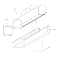
典型的なCISを図1に、同様にCIS用ライン状照明光学系を図2に示す。図1においては、CISの長手方向中央部近傍における断面図が示されている。一方、図2は分解斜視図である。X方向が主走査方向であり、Y方向が副走査方向である。Z方向は、X方向及びY方向に直交している。ライン状の光源部10は、主走査方向に細長い光量分布を有する照明光学系である。
典型的なCISを図1に、同様にCIS用ライン状照明光学系を図2に示す。図1においては、CISの長手方向中央部近傍における断面図が示されている。一方、図2は分解斜視図である。X方向が主走査方向であり、Y方向が副走査方向である。Z方向は、X方向及びY方向に直交している。ライン状の光源部10は、主走査方向に細長い光量分布を有する照明光学系である。
図1に示すCISでは、焦点面(検査面)20を挟んで2つの筐体16が対向配置されている。各筐体16内には、焦点面20上にある検査対象物を照明するためのライン状の光源部10が設けられている。一方の筐体16内には、受光レンズ11及び受光部12が設けられており、照明された検査対象物からの光は、受光レンズ11により受光部12へと導かれる。受光レンズ11は、検査対象物からの光を受光部12に結像する。図1に示すCISでは、焦点面20を基準にして、2つの光源部10のうちの一方が受光部12側に配置され、他方が受光部12側とは反対側に配置されている。
受光部12は、一方の筐体16に固定された基板13に実装されている。受光レンズ11を通過した光は、受光部12の受光面12Aで受光され、その受光量に応じた信号が受光部12から出力される。検査対象物が焦点面20に沿って一方向Yに搬送されることにより、検査対象物からの光が連続的に受光部12で受光され、受光部12からの出力信号に基づいて検査対象物の画像(カラー画像や蛍光画像など)が得られる。このように、副走査方向(Y方向)に搬送される検査対象物は、主走査方向(X方向)に延びる受光部12によって、該受光部12の受光面12Aにより構成される読取ラインで読み取られる。
一方の光源部10から出射された光B3は、筐体16に固定された保護ガラス14を透過して、他方の筐体16に固定された保護ガラス14Aの内面に設けられている反射部材17Aで反射し、焦点面20に導かれる。焦点面20から受光部12までの任意の位置には、受光部12に紫外光が入射するのを阻止する紫外光遮断フィルタ(UVカットフィルタ)15が設けられている。また、受光部12と紫外光遮断フィルタ15との間には、特定波長範囲の可視光を通過させるカラーフィルタ18が設けられている。一方の筐体16内における光源部10の底面に対向する位置には、光源部10に備えられた光源103(紫外光源や可視光源など)を固定するための基板5が設置されている。
図1及び図2に示す例では、光源部10は、長手方向Lに沿って延びる透明な導光体101と、長手方向Lの一方の端面付近に設けられた光源103と、導光体101の各側面を保持するためのカバー部材102とを備えている。光源103から出射した光は、導光体101に入射し、該導光体101中を伝搬しながら光拡散パターンPにより適宜反射され、光出射面から矢印方向に出射し、ライン状の照明光となって検査対象物を照明する。このようなCISの被写界深度は浅く、検査対象物に厚みがある場合は厚み方向全体の検査は困難であり、かつ、W.D.が狭いため、検査対象物に接触し、検査そのものが成立しない場合が多い。
前記のようなCISでは、受光レンズ11として、例えばSELFOC(日本板硝子株式会社製)レンズアレイが用いられる。SELFOCレンズアレイは、正立等倍のレンズアレイである。該レンズアレイでは、円柱状のSELFOCレンズを俵積みし、多眼レンズとしている。多眼レンズの利点は、レンズ単体よりも所謂レンズの明るさを明るくすることが可能であることである。即ち、レンズ単体のFナンバーよりも単体レンズを複数個並べて多眼レンズとした場合のFナンバーのほうが小さい。これは、任意の位置にある1個のレンズの焦点位置と該レンズの周囲のレンズの焦点位置が一致した箇所で、有効Fナンバーが小さくなるからである。逆に言えば、正立レンズ系においては、開口数(以下N.A.と記す)がレンズ単体よりもアレイ化したほうが大きくなることを意味する。この性質が、CISにSELFOCレンズアレイが用いられる大きな理由となっている。
前記のようなCISの利点は、被写界深度及び焦点深度の観点からは、逆に不利となる。単眼レンズでもそうであるように、開口数が大きくなれば、被写界深度は浅くなる。例えば顕微鏡対物レンズでは、倍率が大きくなり、即ちN.A.が大きくなるに従い、被写界深度が浅くなることは、よく知られていることである。また、カメラレンズにおいても、遠景と近景とでは、被写界深度の長短が如実に示され、被写界深度を確保するために絞りで調整している。即ち、N.A.を変化させ、所望の被写界深度を得ている。加えて、SELFOCレンズに代表される正立多眼レンズは、各レンズの光軸が異なり交差するため、単眼レンズと比べ、検査対象物が光軸方向に変化した場合に像がボケ易い構造となっている。上記が俵積み方式の多眼SELFOCレンズアレイの大きな欠点である。そこで、如何にすれば、コンパクトな光学ラインセンサの被写界深度を深くすることが可能であるかを検討した結果、得られた実施例を以下に記す。以下の実施例において、受光レンズ11は、テレセントリック光学系を構成している。
2.受光系の実施例
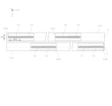
まず、第一の方法は、図3に示すように光学ラインセンサを単眼レンズ化したと見做せるアレイ構造とすることである。図3は、各受光レンズ11の視野が重ならないようにした受光系の模式図である。図3では、各受光レンズ11の視野が重ならないように、各受光レンズ11を主走査方向(X方向)に離間して配置するとともに、各受光レンズ11を副走査方向(Y方向)にも離間させることにより、各受光レンズ11が千鳥状に配置されている。
まず、第一の方法は、図3に示すように光学ラインセンサを単眼レンズ化したと見做せるアレイ構造とすることである。図3は、各受光レンズ11の視野が重ならないようにした受光系の模式図である。図3では、各受光レンズ11の視野が重ならないように、各受光レンズ11を主走査方向(X方向)に離間して配置するとともに、各受光レンズ11を副走査方向(Y方向)にも離間させることにより、各受光レンズ11が千鳥状に配置されている。
即ち、俵積み方式ではなく、主走査方向(X方向)に沿って複数配置された複数の受光レンズ11同士が、互いに離間して配置されている。主走査方向(X方向)に沿って複数配置された複数の受光レンズ11は、レンズホルダー110により一体的に保持されている。各受光レンズ11に対してZ方向に対向する位置には、複数の受光素子(図示せず)が主走査方向(X方向)に沿ってライン状に配置されることにより構成される受光素子アレイ120が配置されている。すなわち、複数の受光素子が、主走査方向(X方向)に沿ってアレイ状に配置されることにより1つの受光素子アレイ120が構成されている。各受光素子は、各受光レンズ11を透過した光を受光する。
この例では、各受光レンズ11に対応付けて受光素子アレイ120が配置されている。これにより、短尺センサからなる各受光素子アレイ120が、主走査方向(X方向)に沿って交互に千鳥状に配置されている。主走査方向(X方向)に沿って複数配置された複数の受光素子アレイ120は、1列の読取ラインLを形成しており、図3の例では2列の読取ラインLが形成されている。レンズホルダー110は、各読取ラインLに対応付けて設けられる構成に限らず、1つのレンズホルダーで各読取ラインLに対応する複数の受光レンズ11を一体的に保持するような構成であってもよい。
この図3に示すように、1つの受光素子アレイ120に対し、1つの受光レンズ11を対応させることにより、複数の受光素子アレイ120に対応した数だけ複数の受光レンズ11が配置されてもよい。各受光レンズ11を透過して各受光素子アレイ120に導かれる光の光軸は、1対1に対応する各受光素子アレイ120の主走査方向(X方向)の略中央部を貫いてもよい。この方式では、複数の受光素子アレイ120を副走査方向(Y方向)に複数列並べる。即ち受光素子の配列方向(X方向)に対して直角方向(Y方向)に離間して、複数列の受光素子アレイ120が配置される。
各受光レンズ11は、副走査方向における幅W1が主走査方向における幅W2(レンズ径)よりも小さい。すなわち、各受光レンズ11は、主走査方向に沿って細長い形状を有している。各受光レンズ11の副走査方向における幅W1は、各受光レンズ11の副走査方向における視野に対応している。また、各受光レンズ11の主走査方向における幅W2は、各受光レンズ11の主走査方向における視野に対応している。各受光レンズ11は、N.A.が0.001<N.A.<0.05を満足するように、副走査方向における幅W1が設定されていることが好ましい。この例では、各受光レンズ11が同一形状を有しており、それぞれ主走査方向及び副走査方向に直交する方向(Z方向)から見て矩形状に形成されている。ただし、各受光レンズ11は、矩形(長方形)に限らず、長円形又は楕円形であってもよいし、他の形状であってもよい。
複数の受光レンズ11は、該受光レンズの主走査方向における幅W2以下に互いに離間して配置されている。すなわち、複数の受光レンズ11は、該受光レンズ11の主走査方向における視野寸法以下(視野範囲内)に互いに離間して配置されていることが好ましい。図3の例のように、副走査方向において各受光レンズ11の視野を重畳させてもよい。この場合は、複数の受光レンズ11の視野が重なった部分の受光素子について、該受光素子からの画素出力を減算処理すればよい。例えば、該受光素子より出力されたデータから一方の受光レンズ11の画像(一方の受光レンズ11を透過した光の受光量)を除外するか、或いは、画像合成する際に該受光素子からの画素出力を略半分の出力値とすればよい。複数の受光素子列(受光素子アレイ120)を用いれば、画素欠落の発生を1ラインの受光素子列の場合よりも確実に防止できる。
図4は、複数の受光素子アレイ120が配置された受光系の他の例を示した模式図である。図4の例では、各受光レンズ11と各受光素子アレイ120が1対1に対応するのではなく、主走査方向に並ぶ複数(この例では2つ)の受光レンズ11が1つの受光素子アレイ120に対応している。
1つの受光素子アレイ120に対応する複数の受光レンズ11は、主走査方向に隣接している。ただし、1つの受光素子アレイ120に対応する複数の受光レンズ11は、互いに離間していてもよく、この場合、受光レンズ11の主走査方向における幅W2以下に互いに離間していてもよい。また、各受光レンズ11の間には、遮光部材が設けられていてもよい。
図5は、複数の受光素子アレイ120が配置された受光系のさらに他の例を示した模式図である。図5では、同じ長さの長尺センサ(主走査方向全長に対応した長さ)からなる各受光素子アレイ120が、副走査方向に並べて平行に複数(この例では2つ)配置されている。この図5に示すように、主走査方向(X方向)に並ぶ複数の受光レンズ11に対し、1つの受光素子アレイ120を対応させることにより、副走査方向(Y方向)の受光レンズ11の列の数だけ複数の受光素子アレイ120が配置されてもよい。
図3~図5のいずれにおいても、受光レンズ11の副走査方向における幅W1が主走査方向における幅W2よりも小さいため、受光レンズ11を副走査方向に近づけて配置することができ、その結果、光学ラインセンサをコンパクト化することができる。上記のように、短尺の受光素子アレイ120を千鳥状配列して用いるか(図3及び図4参照)、或いは、2列の受光素子アレイ120を離間して配置して用いてもよいが(図5参照)、これに限らず、更に多くの複数の受光素子アレイ120を副走査方向(Y方向)に離間して配置してもよい。
3.受光レンズの長焦点化
次に、受光レンズの長焦点化について述べる。従来のSELFOCレンズはCISのコンパクト化やコストダウンに重きを置き、共役長のより短いレンズが求められてきた。しかしながら、この流れは、許容される被写界深度を減じてしまうことを助長する要因となっている。しかもレンズ径は益々小さくなってきている。受光レンズを長焦点化する場合、従来の受光レンズを利用すると、N.A.が極端に小さくなる。故に回折の影響が大きくなり、受光レンズ自身の有する幾何光学的な収差によるボケよりも回折限界によるボケが光学的分解能劣化の支配要因となる。従来方式のCISは、N.A.が大きいため、回折限界による像のボケが生じることを無視出来ていた。しかし、W.D.を長くとるためには、受光レンズの焦点距離を延ばすことが必要であり、即ち、N.A.が小さくなってしまうため、従来のレンズ径では、焦点距離が増大すればするほど回折の影響もそれに伴い増大する。本実施形態では、レンズ径を大きくすることでW.D.を長くし、回折限界による像のボケを減じた場合においても、光学的分解能を劣化させない方法を提案する。
次に、受光レンズの長焦点化について述べる。従来のSELFOCレンズはCISのコンパクト化やコストダウンに重きを置き、共役長のより短いレンズが求められてきた。しかしながら、この流れは、許容される被写界深度を減じてしまうことを助長する要因となっている。しかもレンズ径は益々小さくなってきている。受光レンズを長焦点化する場合、従来の受光レンズを利用すると、N.A.が極端に小さくなる。故に回折の影響が大きくなり、受光レンズ自身の有する幾何光学的な収差によるボケよりも回折限界によるボケが光学的分解能劣化の支配要因となる。従来方式のCISは、N.A.が大きいため、回折限界による像のボケが生じることを無視出来ていた。しかし、W.D.を長くとるためには、受光レンズの焦点距離を延ばすことが必要であり、即ち、N.A.が小さくなってしまうため、従来のレンズ径では、焦点距離が増大すればするほど回折の影響もそれに伴い増大する。本実施形態では、レンズ径を大きくすることでW.D.を長くし、回折限界による像のボケを減じた場合においても、光学的分解能を劣化させない方法を提案する。
アッベの回折限界dは、開口数N.A.に逆比例する。光学系は空気中にあるため、空気中の波長λを用いて下記式1が成り立つ。
d=λ/N.A. (式1)
図6に各波長に対するN.A.と回折限界の関係を表す。同じレンズパラメータの受光レンズ11においては、受光レンズ11自身の所謂ピッチを短くすれば焦点距離は伸び、収差の影響も少なくなる。
d=λ/N.A. (式1)
図6に各波長に対するN.A.と回折限界の関係を表す。同じレンズパラメータの受光レンズ11においては、受光レンズ11自身の所謂ピッチを短くすれば焦点距離は伸び、収差の影響も少なくなる。
以上より、受光レンズ11を長焦点化するためには、レンズ径をより大きくする必要があることが分かる。N.A.を同一に保てば、回折の影響を短い焦点の受光レンズ11と同等にできる。しかしながら、レンズ径を大きくすると幾何光学的収差が大きくなる。そこで、レンズパラメータの異なる受光レンズ11において、レンズ径を大きくした場合の最小錯乱円径を検討する必要がある。波長λは、回折限界径の大きいλ=630nmとした。
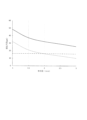
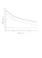
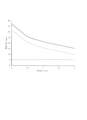
本願発明者による検討の結果、ある受光レンズ11の各焦点距離に対する最小錯乱円の関係を考えればよいことが判明した。例えば、焦点距離fがf=50mmの場合を図7A~図7Cに示す。ここでは、受光レンズ11として3種類のSELFOCレンズ(SELFOCレンズA、SELFOCレンズB及びSELFOCレンズC)を用いた場合に、図7AはSELFOCレンズAの有効径と錯乱円径の関係、図7BはSELFOCレンズBの有効径と錯乱円径の関係、図7CはSELFOCレンズCの有効径と錯乱円径の関係をそれぞれ示している。図7A~図7Cにおいて、実線はトータルの錯乱円、破線は回折による錯乱円、一点鎖線は幾何光学的錯乱円をそれぞれ示している。
図6と図7Aによれば、最小錯乱円と回折限界の関係、即ち、あるレンズ径と焦点距離における光学的分解能が分かる。故に、図7Aに示した受光レンズ11の場合は、有効径Φが大きくなるほど、錯乱円径が小さくなり、有効径Φが1.0mm≦Φ≦3.0mmであれば良いことが分かる。
一方、図6と図7Bによれば幾何光学的錯乱円が大きく、回折による依存度が少なくなるため、Φ=1.0mmの錯乱円径が一番小さい。しかも、Φ=1.0mmのときでも、図7Aに示した受光レンズ11の倍近くの錯乱円径となる。図7Aに示した受光レンズ11は、図7Bに示した受光レンズ11よりも収差が小さく、有効径が大きいSELFOCレンズであり、図7Aの受光レンズ11を選択すべきであることが分かる。更に、同じ焦点距離である図7Aの受光レンズ11は、図7Bの受光レンズ11よりもN.A.が少なくとも3倍は大きくでき、即ち、受光光量は、9倍以上になり、故に、受光素子の出力も9倍以上になる。それに伴い受光素子の受光光量に依存するショットノイズも1/3に減じられるため、ノイズ抑制の観点からも図7Aに示した受光レンズ11が好ましい。また、同じノイズ量が許容される場合は、図7Aの受光レンズ11が図7Bの受光レンズ11に比べ、9倍に走査速度を向上させることが出来るとも言える。
図7Cによれば、SELFOCレンズCもSELFOCレンズAと同様に収差が少なく、有効径を大きくとることが可能である。
次に、図7A~図7Cに示したSELFOCレンズA~Cのパラメータを下記表1に示す。表1に示した中で最も重要なパラメータは屈折率分布定数である。有効径を拡大し、焦点距離を伸ばした際に収差が少ない受光レンズ11は、屈折率分布定数が最も小さいSELFOCレンズAであり、次に収差が少ない受光レンズ11は、SELFOCレンズCである。高解像度で高速検査を目指すには、有効径が大きくて明るく、収差の少ない受光レンズ11が好ましいことは言うまでもない。

更に、受光レンズ11として4種類のプラスチックロッドレンズ(プラスチック屈折率分布型レンズ)を用いた場合に、図8AはロッドレンズAの有効径と錯乱円径の関係、図8BはロッドレンズBの有効径と錯乱円径の関係、図8CはロッドレンズCの有効径と錯乱円径の関係、図8DはロッドレンズDの有効径と錯乱円径の関係をそれぞれ示している。図8A~図8Dにおいて、実線はトータルの錯乱円、破線は回折による錯乱円、一点鎖線は幾何光学的錯乱円をそれぞれ示している。また、図8A~図8Dに示したロッドレンズA~Dのパラメータを下記表2に示す。プラスチックロッドレンズにおいてもSELFOCレンズと同様の傾向があることが分かる。プラスチックロッドレンズの屈折率、及びガラスレンズの屈折率を考慮すると、軸上屈折率は、1.45程度から1.65程度が好ましい。

以上より、屈折率分布定数が収差の支配要因であることが分かる。理想的な屈折率分布型レンズであれば、屈折率が緩やかに変化すればするほど収差は少なくなる。これは、通常の球面レンズであっても急激な角度変化が収差の発生要因であるのと同様である。急激な角度変化は、Snell’Lawを多項式展開した際の高次の非線形効果の増大を意味する。即ち、近軸光学からの逸脱が大きくなるために収差が大きくなるのである。本願発明者は、焦点距離、或いは、W.D.を略50mm以上、有効径Φが略Φ≧1.0mmにおいて、解像度が400dpi以上の画素分解能を達成するために、屈折率分布定数を0.12以下にすることが好ましいことを見出した。
4.受光レンズの変形例
本願発明における受光レンズ11は、SELFOCレンズやプラスチックロッドレンズなどの屈折率分布型のレンズに限らず、他のレンズ、例えば、アクロマート(色消し)、アポクロマートなどにおいて、コストを考慮し、前記の屈折率分布型レンズにおける非線形効果による収差を同等にした、即ち球面収差、コマ収差、非点収差を同等にしたレンズ、或いは、テレセントリック屈折光学系を前記の屈折率分布型レンズにおける非線形効果による収差および回折限界が同等のSELFOCレンズやプラスチックロッドレンズなどの屈折率分布型のレンズに代えて同様な配置や寸法(口径)で用いることも可能である。これは、後述する倒立像を形成する受光レンズ11においても同様である。
本願発明における受光レンズ11は、SELFOCレンズやプラスチックロッドレンズなどの屈折率分布型のレンズに限らず、他のレンズ、例えば、アクロマート(色消し)、アポクロマートなどにおいて、コストを考慮し、前記の屈折率分布型レンズにおける非線形効果による収差を同等にした、即ち球面収差、コマ収差、非点収差を同等にしたレンズ、或いは、テレセントリック屈折光学系を前記の屈折率分布型レンズにおける非線形効果による収差および回折限界が同等のSELFOCレンズやプラスチックロッドレンズなどの屈折率分布型のレンズに代えて同様な配置や寸法(口径)で用いることも可能である。これは、後述する倒立像を形成する受光レンズ11においても同様である。
前述した光学系は、正立レンズを中心にした場合であるが、視野が重ならない場合においては倒立光学系であってもよい。すなわち、複数の受光レンズ11が、倒立像を形成するような構成であってもよい。2列方式のレンズアレイであれば、倒立光学系の採用も可能である。倒立光学系の場合は、像が光軸を中心に反転対称となるため、画像合成する際に画像処理によって倒立像を正立像に変換すればよい。すなわち、複数の受光レンズ11の反転像を反転させ、正立像に変換した後に画像合成処理をすればよい。また、その操作の過程で、補正アルゴリズムから重なり合った部分の要又は不要を決定及び補正し、決定した画素間の関係から正立像に変換すればよい。或いは、画像を構築しない場合の検査においては、キズ又は欠陥を検出するのみでよいため、画像合成並びに画像処理の必要はなく、検査面における検出部分が重畳していてもよい。重畳する場合は、予め補正チャートによる位置の補正をしておく。
更に、倒立型屈折光学系の場合は、各受光素子に対する信号処理において、例えば、副走査方向に離間するように千鳥配置された2列の受光素子アレイの一方から得たデータを長めに取得し、他方の受光素子アレイから得たデータを短めに取得し、取得した像の正立像への反転操作を行った後に、画像合成してもよい。或いは、各受光素子の倒立像データを正立像に各々変換した後に、画像合成する際に重なり合った部分に補正係数を掛けるか減算してもよい。
具体的には、倒立型屈折光学系において、複数の受光素子アレイが、2列の読取ラインにそれぞれ複数配置された各読取ラインよりも短い受光素子アレイであってもよい。また、一方の読取ラインに配置された受光素子アレイと他方の読取ラインに配置された受光素子アレイとが、主走査方向に沿って交互に千鳥状に配置されていてもよい。このような構成は、図3において説明した正立型屈折光学系の場合と同様であるため、詳細な説明を省略する。
この場合、図3に示すように、複数の受光素子は、2列以上のアレイ状に配置されることにより複数の受光素子アレイ120を構成している。また、複数の受光素子アレイ120の各々は、読取ラインLに直交する方向において受光レンズ11の主走査方向における幅W2以下に互いに離間して配置されている。複数の受光レンズ11は、複数の受光素子アレイ120に対応した数だけ配置され、各受光レンズ11を透過して各受光素子アレイ120に導かれる光の光軸は、各受光素子アレイ120の略中央部を貫く。ただし、各受光レンズ11を透過して各受光素子アレイ120に導かれる光の光軸は、各受光素子アレイ120の略中央部から副走査方向に平行に離れた位置を貫いていてもよい。
5.照明光学系の構成
本実施例において、受光レンズ11の焦点距離fは、f=50mm、N.A.は、N.A.=0.01、0.02、0.025、0.03とし、屈折率分布定数√Aは、√A=0.077とした。光源103に関しては、W.D.が従来のCISに比べて10倍以上長いため、等倍系では、検査面照度は100倍以上を必要とする。そのため、光源103として、例えば高輝度の白色LEDアレイを用いる。すなわち、複数の光源103が、白色LEDを含む構成であってもよい。可視域の半導体レーザを光源103として用いる場合は、出射ビームを主走査方向に拡大し、副走査方向にコリメーションすることで照射時の光量ムラを低減する。
本実施例において、受光レンズ11の焦点距離fは、f=50mm、N.A.は、N.A.=0.01、0.02、0.025、0.03とし、屈折率分布定数√Aは、√A=0.077とした。光源103に関しては、W.D.が従来のCISに比べて10倍以上長いため、等倍系では、検査面照度は100倍以上を必要とする。そのため、光源103として、例えば高輝度の白色LEDアレイを用いる。すなわち、複数の光源103が、白色LEDを含む構成であってもよい。可視域の半導体レーザを光源103として用いる場合は、出射ビームを主走査方向に拡大し、副走査方向にコリメーションすることで照射時の光量ムラを低減する。
RGB-LED、或いは、RGB-LD(レーザダイオード;半導体レーザ)を光源103として用いる場合の配置方法の1例を図9Aに示す。このように、複数の光源103が、赤色LED(R)、緑色LED(G)及び青色LED(B)を含む構成であってもよいし、レーザダイオードを含む構成であってもよい。図9Aにおいて、複数の光源103は光源基板134に実装されており、光源基板134にはヒートシンク135が取り付けられている。各光源103から出射されたビームは、主走査方向と副走査方向とでレンズパワーが異なる楕円体形状の集光レンズ104でコリメートされ、検査対象物に照射される。ここでは、楕円体形状の集光レンズ104を示したが、主走査方向と副走査方向とで適宜レンズパワーが異なるレンズであればよい。なお、レンズのパワーとは、焦点距離の逆数であり、レンズの屈折力を表す尺度である。
或いは、LDに関しては、LD自身の出射ビームの拡がり角が水平方向及び垂直方向で異なる端面発光型のLDを用いれば、通常のコリメータレンズでもよい。図9Bは、LDを光源103として用いる場合の配置方法の具体例を示した側面図である。この場合は、拡がり角が大きいほうのLDを主走査方向に対して平行に配置する。光源103を構成する赤色LD131、緑色LD132及び青色LD133から出射されたビームは、それぞれに対応付けられた集光レンズ104でコリメートされた後、シリンドリカルレンズ105により検査面に絞り込まれる。こうすることで、RGBの各色が副走査方向においてほぼ同じ位置に照射され、副走査方向に対する色ムラを低減することが可能になる。一方、LEDやLDなどの光源103により照射され、検査面で拡散反射された光は、受光レンズ系で受光素子アレイに結像される。受光素子は、等倍光学系では、400dpi相当の62μmの素子サイズから600dpi相当の42μmの素子サイズを用いる。600dpi以上の素子サイズを用いる場合は、照明光のパワーをそれに応じて増大させればよい。このように、複数の光源103が、複数の異なる波長を有する光源131~133を含み、該光源131~133を1単位として、該1単位の光源103が主走査方向(X方向)に複数並べられた構成であってもよい。
更に、単位面積当たりの放射輝度が同じであっても受光素子のサイズが異なれば、発光部の面積が異なることと同義になるため、受光素子面積のほぼ二乗に逆比例して受光光量が低下する。以上を考慮し、照明光量を決定する。素子サイズが小さくなると、同じ蓄積時間では、素子面積に逆比例して受光光量が減少する。これは半導体受光素子の物理的な性質であり、S/Nを維持するためには、照明光を増大させて、パワー密度を増大させ、単位時間に発生する生成電子数を同数にすればよい。これにより、ショットノイズを受光素子のサイズが減少しても大きなサイズの受光素子と同等に維持できる。また、受光素子が受光する光は、検査面の照度だけでなく、受光する際に受光素子の見ている範囲にも依存する。言うまでもなく受光立体角が異なり、その角度が減少すれば、受光量も減少し、検査面が完全拡散面であれば、所謂cosθ則に応じた受光光量となる。検査面上から拡散反射された光は、受光レンズにより補足され受光素子に集光され、その出力信号が、受光素子から出力される。また、受光素子列からの出力信号は、シリアルからパラレルに分岐されて、処理速度を向上させ、画像処理装置に伝達される。
図10Aは、光源103と受光レンズ11の位置関係を示した模式図であり、受光素子アレイ120が2列の場合である。図10Aでは、2列に配列した受光レンズ11並びに受光素子アレイ120に対する光源103の配置が示されている。本実施例では、光源103が2列の読取ラインLの略中央部に配置されている。各光源103は、読取ラインLに平行に並べて配置されている。また、各光源103の光軸は、各受光レンズ11を透過して各受光素子アレイ120に導かれる光の光軸と交点を結び、かつ各受光レンズ11を透過して各受光素子アレイ120に導かれる光の光軸と交差する仮想平面の任意の位置に配置されている。本実施例においては、受光レンズ11の焦点距離fがf=50mm、レンズ径ΦがΦ=4mm(但し、幾何光学的収差を考慮し、アパーチャーを用いて有効径Φ’はΦ’=2.5mmとした)である。本実施例では、検査面に対して、約45度の角度で光源103から光が照射される。そのため、受光レンズ11のW.D.を考慮し、光源103と検査面との距離は70mmとした。本実施例では、LDを用いたが、各波長のLEDを用いてもよい。
光源103の配列ピッチはレンズ間距離に合わせ、互いに隣接する受光レンズ11の間の略中央部であると同時に2列の読取ラインLの略中央部である位置に光源103が配置されている。こうすることにより検査面上の画素の欠落をより防止出来ると同時に、受光レンズ11のシェーディング並びに光源103の光量ムラをより低減出来る。各列の受光レンズ11間のレンズピッチを7mmとした。この場合、実質的なレンズピッチは、3.5mmとなる。
図10Bは、主走査方向における光源103(検査面上)の光量分布、受光素子面上の光量分布、受光レンズ11のシェーディングの関係を示した図である。図10Aのレイアウトにおいて、受光素子アレイ120上の光量分布は、模式的に図10Bで示すようにフラットになり、受光素子のダイナミックレンジを有効に用いることが可能になる。
6.リップルの抑制方法
次に、個々の受光レンズ11に起因するシェーディングが読取ラインL方向に対するリップルを発生させ、ひいては、受光素子のダイナミックレンジを狭くすることに繋がるのであるが、この抑制方法について述べる。
次に、個々の受光レンズ11に起因するシェーディングが読取ラインL方向に対するリップルを発生させ、ひいては、受光素子のダイナミックレンジを狭くすることに繋がるのであるが、この抑制方法について述べる。
まず、予め照明系により負の強度分布を有する照明光を検査対象物に照射しておく。例えば、隣接する受光レンズ11の間に光源103を配置する方法では、完全に各種の受光レンズ11に対応したシェーディング抑制方法にはならない。即ち、個々の受光レンズ11に特有のシェーディングが存在し、受光レンズ11が異なれば、それに応じた照明光学系を用いなければならない。本実施形態では、主走査方向に大きいパワーを有する集光レンズ104が配置される。該集光レンズ104を透過した光束は、次にシリンドリカルレンズ105などの収束レンズにより検査対象物に導かれ、受光レンズ11のシェーディングに応じた光強度を検査対象物上に形成する。そして、受光レンズ11のシェーディングに応じて、集光レンズ104の光軸方向の位置を適宜変更することで、例えば、検査対象物がキャリブレーション用の白色基準板であれば受光素子上の光強度分布を平滑化出来る。前記の集光レンズ104は副走査方向にパワーを有していてもよい。要するに、受光レンズ11のシェーディングを完全なまでに抑制し、かつ検査対象物に対し受光レンズ11の焦点距離を考慮した有効な光強度分布が同時に実現出来ればよい。即ち、主走査方向のレンズパワーが副走査方向のレンズパワーよりも大きいことが好ましい。集光レンズ104としては、例えば、シリンドリカルレンズ、レンチキュラーレンズ、フレネルレンズ、又は、プリズムシートと球面レンズの組み合わせなどが好ましい。光源103の主走査方向に対する位置関係は、各受光レンズ11の中間位置に配置してもよいし、受光レンズ11の光軸上に配置してもよい。更には、受光レンズ11の外周の位置に光源103を配置してもよい。また更に主走査方向にパワーの分布を有するレンズであればより好ましい。
本実施形態では、複数の光源103からの光束を集光する集光レンズ104が、1個のレンズ体として設けられており、該レンズ体が有する主走査方向のパワーが副走査方向のパワーよりも大きい。ただし、集光レンズ104が、1個のレンズ体ではなく、第1集光レンズ及び第2集光レンズを含む構成であってもよい。この場合、第1集光レンズは、主走査方向のパワーが副走査方向のパワーよりも大きく、第2集光レンズは、副走査方向のパワーが主走査方向のパワーよりも大きくてもよい。また、主走査方向のパワーを第1集光レンズと第2集光レンズにより調整可能であってもよい。
上記のような第1集光レンズ及び第2集光レンズを備えた集光レンズ104において、第1集光レンズ及び第2集光レンズは、シリンドリカルレンズ、レンチキュラーレンズ、フレネルレンズ、又は、プリズム列などにより構成することができる。例えば、第1集光レンズは、レンチキュラーレンズ或いはプリズム列であってもよい。また、第2集光レンズは、フレネルレンズ或いはシリンドリカルレンズであってもよい。
7.受光レンズのパラメータ
本実施形態におけるレンズ径別の受光系MTFのグラフを図10Cに示す。比較例として、図10Dに屈折率分布定数√A=0.154の場合を示す。実線、短破線、長破線、一点鎖線の順番に、有効径ΦがΦ=1.0、1.5、2.0、2.5、3.0mmの場合を示している。尚、受光素子の画素寸法は、600dpi相当に合わせ主走査方向、副走査方向とも42.3μmとしている。
本実施形態におけるレンズ径別の受光系MTFのグラフを図10Cに示す。比較例として、図10Dに屈折率分布定数√A=0.154の場合を示す。実線、短破線、長破線、一点鎖線の順番に、有効径ΦがΦ=1.0、1.5、2.0、2.5、3.0mmの場合を示している。尚、受光素子の画素寸法は、600dpi相当に合わせ主走査方向、副走査方向とも42.3μmとしている。
本実施形態では、有効径Φにおいて、屈折率分布定数√Aが√A=0.077の条件では、600dpi相当の12ライン/mmで30%程度の性能であれば、Φ1.0mmからΦ3.0mmまでの範囲のMTF特性を満足している。それに対し、比較例は、有効径Φについてすべての範囲でMTF特性を満足していない。これは、√Aが√A=0.077の場合の方が√A=0.154の場合よりも収差特性が優れていることを示している。また、焦点距離f=50mmの場合について、屈折率分布定数√Aが√A=0.1027の場合の受光光学系のMTFを求め、図10Eに示す。図10Eによれば、√Aが√A=0.1027の場合においても、600dpiの解像度に相当する12ライン/mmでΦ1.0mmからΦ3.0mmまでの範囲においてMTF特性を満足している。
受光レンズ11が屈折率分布型レンズである場合、該レンズはガラス或いは樹脂からなることが好ましい。この場合、受光レンズ11のレンズパラメータにおいて、軸上屈折率N0が1.45≦N0≦1.65であり、屈折率分布定数√Aが0.05≦√A≦0.12であり、焦点距離fが50mm≦f≦150mmであることが好ましい。
受光レンズ11は、それぞれ複数枚のレンズを組み合わせたアクロマート又はアポクロマートであってもよい。この場合、複数枚のレンズとして凸レンズのみを組み合わせたレンズ系であるか、或いは、複数枚のレンズとして凸レンズと凹レンズを組み合わせたレンズ系であってもよい。また、複数枚のレンズの焦点距離fが25mm≦f≦250mmであり、更に複数枚のレンズの口径Φが2mm≦Φ≦50mmであることが好ましい。
次に、被写界深度並びに解像度を向上させるために、受光レンズ系を縮小光学系としたものを例示する。光学系の構成は図10Aと同様であり、受光レンズ11の倍率を変化させている。即ち、受光レンズ11の物点と像点の横倍率の関係を9:1や4:1のように変化させる。こうすることにより、被写界深度は、横倍率が9:1の場合は等倍系の3倍に、横倍率が4:1の場合は等倍系の2倍に増大する。被写界深度を3倍とする場合には、受光素子のサイズは等倍系の受光素子の1/9のサイズとする。また、被写界深度を2倍とする場合には、受光素子のサイズは等倍系の受光素子の1/4のサイズとする。本実施形態においては、1/4のサイズの受光素子を用いて、被写界深度を2倍とした。
本実施形態における縮小光学系のデフォーカス時のMTF特性を図11のグラフ(実線)に示す。比較例として、等倍系のデフォーカス時のMTF特性を図11のグラフ(破線)に示す。図の縮小系と等倍系の比較から、縮小光学系の被写界深度が等倍系よりも約2倍深いことが分かる。また、受光レンズ11のN.A.は、縮小比をSとすれば、その逆数である1/Sだけ増大する。そのため、受光レンズ11のレンズ径が小さい場合においても、焦点距離に応じて縮小率を増せば、実効的なN.A.は維持されるため、回折効果によるボケも一定に出来る。
本実施形態では、焦点距離をf=50mm、横倍率比を1/4としたため、レンズ径Φは原理的にはΦ=0.25mmまで用いることが可能である。図10Aの場合と同じレンズを用いるので、レンズ径ΦはΦ=4mmであり、有効径Φ’はΦ’=2.5mmである。N.A.は、等倍系である図10Aの場合と比べて4倍になる。故に受光光量は16倍になり、受光素子サイズを1/4にサイズダウンしたことによる受光光量の1/16の減少を相殺出来る。
9.テレセントリック光学系
次に本実施形態に適用されたテレセントリック光学系について説明する。テレセントリック光学系を用いることにより、組み立て容易で経時変化が少ない構成にすることができる。テレセントリック光学系では、アパチャー(光透過部)を挟んで両側又は片方に受光レンズ11が配置される。すなわち、テレセントリック光学系は、検査対象物側と受光素子アレイ120側の両方に受光レンズ11が配置された両側テレセントリック光学系、又は、検査対象物側のみに受光レンズ11が配置された物体側テレセントリック光学系である。
次に本実施形態に適用されたテレセントリック光学系について説明する。テレセントリック光学系を用いることにより、組み立て容易で経時変化が少ない構成にすることができる。テレセントリック光学系では、アパチャー(光透過部)を挟んで両側又は片方に受光レンズ11が配置される。すなわち、テレセントリック光学系は、検査対象物側と受光素子アレイ120側の両方に受光レンズ11が配置された両側テレセントリック光学系、又は、検査対象物側のみに受光レンズ11が配置された物体側テレセントリック光学系である。
両側テレセントリック光学系では、検査対象物から光軸に平行に細く拡がる光束が前側レンズを透過することにより平行光束となり、前側レンズの後に挿入されたアパチャーを通過した平行光束が、後側レンズを透過して受光素子アレイ120の各受光素子に絞り込まれる。
図3又は図4のように、受光素子アレイ120が副走査方向に千鳥配置となっている場合は、副走査方向の距離が大きくなるほど、メモリ容量を大きくする必要がある。メモリ容量が大きくなれば、それだけコストアップしてしまう。本実施形態においては、テレセントリックレンズ光学系を用いることにより、N.A.を0.03程度とすると、焦点距離が50mmのレンズの場合、レンズの主平面状でΦ=3mmと物点とを結ぶ円錐形の受光立体角となる。故に、副走査方向の千鳥配置の受光素子アレイ120の最短距離Lsは、Ls>3mmであればこと足りる。したがって、通常のレンズの円形の外周部を各種加工又は成型手段により矩形の外周部とし、図3又は図4のように受光素子アレイ120の千鳥配置の間隔を狭くして配置すれば、受光立体角を満足しコンパクト化が可能になると同時にメモリ容量を小さく出来る。尚、受光レンズ11のN.A.は、照明光量の観点から0.001~0.05程度が望ましい。以上、副走査方向の受光レンズ11の厚みは、テレセントリック光学系のN.A.で規定される立体角によって決定されるため副走査方向に短くでき、コンパクトになる。
10.受光系の変形例
次に、図12A~図12Gを用いて受光系の変形例について説明する。上記実施形態では、複数の受光レンズ11が副走査方向に2列で配置された構成について説明したが、図12A~図12Gでは、複数の受光レンズ11が主走査方向に沿って1列に配置された構成、具体的には、1列の受光レンズ11と千鳥配置の受光素子アレイ120のレイアウトについて説明する。
次に、図12A~図12Gを用いて受光系の変形例について説明する。上記実施形態では、複数の受光レンズ11が副走査方向に2列で配置された構成について説明したが、図12A~図12Gでは、複数の受光レンズ11が主走査方向に沿って1列に配置された構成、具体的には、1列の受光レンズ11と千鳥配置の受光素子アレイ120のレイアウトについて説明する。
受光素子アレイ120を千鳥配置することにより2列の読取ラインLを形成する場合、受光素子アレイ120と同様に受光レンズ11も2列に千鳥配置すると、受光レンズ系の必要なN.A.を満足させるために、受光レンズ11の副走査方向の幅以上に受光素子アレイ120の副走査方向の間隔を設ける必要があった。そこで、図12A~図12Gのように、受光レンズ11を受光系に必要なN.A.を満足させるように矩形レンズの幅を設定し、2列から1列にすれば、受光素子アレイ120の副走査方向の間隔をより狭めることが可能になる。即ち、副走査方向の速度変動の影響をより少なくし、同時に、受光レンズ11のコストダウンが達成できる。以下、複数の受光レンズ11を1列に配置する方法について記す。
図12A~図12Gでは、複数の受光レンズ11が、それぞれ主走査方向に対し垂直な方向から見たときに同じ形状を有する。具体的には、主走査方向(X方向)及び副走査方向(Y方向)に対し垂直なZ方向から見たときの各受光レンズ11の形状が同じ形状である。なお、「同じ形状」には、反転形状などの実質的に同じ形状が含まれ、若干の形状の相違は「同じ形状」に含まれるものとする。
図12Aでは、Z方向に見た各受光レンズ11の形状が平行四辺形形状である。すなわち、各受光レンズ11の主走査方向の両端面が、副走査方向に対して傾斜している。各受光レンズ11の主走査方向の両端面の傾斜角は、同一である。図12Aのように主走査方向に複数の受光レンズ11を並べて配置した場合、各受光レンズ11の両端面に、隣り合う受光レンズ11の端面が対向することにより、主走査方向に隣り合う受光レンズ11の端部同士が連結された状態で配置される。
図12Bでは、Z方向に見た各受光レンズ11の主走査方向の両端面に、矩形形状の切り欠きが形成されている。図12Bのように主走査方向に複数の受光レンズ11を並べて配置した場合、各受光レンズ11の両端面に形成された切り欠きに、隣り合う受光レンズ11の一部が嵌め合わせられることにより、主走査方向に隣り合う受光レンズ11の端部同士が連結された状態で配置される。
図12Cでは、Z方向に見た各受光レンズ11の形状が台形形状である。すなわち、各受光レンズ11の主走査方向の両端面が、副走査方向に対して傾斜している。各受光レンズ11をZ方向に見た形状は、主走査方向に隣り合う受光レンズ11をZ方向に見た形状に対して、主走査方向を基準に反転形状である。図12Cのように主走査方向に複数の受光レンズ11を並べて配置した場合、各受光レンズ11の両端面に、隣り合う受光レンズ11の端面が対向することにより、主走査方向に隣り合う受光レンズ11の端部同士が連結された状態で配置される。これにより、複数の受光レンズ11は、隣り合う受光レンズ11が反転し連結された状態で配置される。
図12Dでは、Z方向に見た各受光レンズ11の主走査方向の両端面に、曲線形状(半円形状又は半楕円形状)の切り欠きが形成されている。図12Dのように主走査方向に複数の受光レンズ11を並べて配置した場合、各受光レンズ11の両端面に形成された切り欠きに、隣り合う受光レンズ11の一部が嵌め合わせられることにより、主走査方向に隣り合う受光レンズ11の端部同士が連結された状態で配置される。
次に、図12E~図12Gの変形例について説明する。図12Eは、図12Cの変形例であり、前述した受光素子アレイ120に欠落画素を極力生じさせないように出来る。図12Eでは台形状の各受光レンズ11の幅方向の中央部よりも長辺側に各受光素子アレイ120を配置している。また、各受光素子アレイ120の主走査方向の長さは、該受光素子アレイ120が配置された位置における前記台形状の各受光レンズ11の主走査方向の長さにほぼ一致している。こうすることにより、図12Eの破線で示した部分が隣り合う千鳥配置の受光素子アレイ120同士が主走査方向においてオーバーラップし、後述するように、図12Cで示した千鳥配置の受光素子アレイ120のような出力信号の欠落部を生じない。
上記は、台形状の受光レンズ11に限らず、各々の受光レンズ11を副走査方向に反転させて受光レンズアレイとした際に連結される形状であればよい。その例を図12F及び図12Gに示す。図12Fは矩形の切り欠き形状からなる複数の受光レンズ11を反転し連結させた場合であり、図12Gは、円形の切り欠きを有する複数の受光レンズ11を反転し連結させた場合である。このように、図12E~図12Gにおいて、複数の受光レンズ11は、隣り合う受光レンズ11が反転し連結された状態で配置される。概ね、副走査方向において受光レンズ11が線対象であれば反転連結可能である。図12F及び図12Gも図12Eの台形形状の反転連結と同様に破線部がオーバーラップしており、後述するように、信号欠落部を生じない。なお、図12Gの受光レンズ11は、剛性を確保し、割れを回避するための縁部112を備えている。
図12A~図12Gのように、受光レンズ11の光軸方向断面視においてレンズ端部を平行四辺形形状、台形形状、矩形形状又は曲線形状(円、楕円)の切り欠き形状などの断面形状として受光レンズ系のN.A.を満足する副走査方向の幅を設定し、1列に繋ぐことにより、主走査方向に一直線状に延びるレンズアレイが形成される。また、前記レンズアレイの副走査方向の中央部に、千鳥配置の2列の受光素子アレイ120を設ける。具体的には、複数の受光素子アレイ120が、複数の受光レンズ11のそれぞれの主走査方向の中央部に配置され、主走査方向に沿って交互に千鳥状に配置される。こうすることにより、1列のレンズアレイで2列の千鳥配置の受光素子アレイ120に検査対象物から出射された光を届けることが出来る。
図12Aに示すように、主走査方向に隣り合う受光レンズ11の端部間には、遮蔽部111が設けられている。遮蔽部111は、薄肉の板状に形成されている。遮蔽部111は、各受光レンズ11の端部間から受光素子(受光素子アレイ120)に向かって延長され、受光レンズ11から検査対象物方向に突出している。また、遮蔽部111は、少なくとも受光レンズ11の副走査方向の幅W1以上の幅を有する。図12B~図12Gでは遮蔽部111を省略して示しているが、同様に遮蔽部111が各受光レンズ11の端部間に設けられていてもよい。尚、図12Fと図12Gの実施例において、遮蔽部111は各々薄いクランク型、波型の遮蔽板とする。要は、連結部において、隣り合う受光系に光が漏れ出ないようにすればよい。
図12B~図12Dに示すように、複数の受光素子アレイ120と一対一に対応するように、検査対象物を照明する複数の光源103が設けられていてもよい。複数の光源103は、それぞれ主走査方向に沿って一直線状に延びる細長い形状であってもよく、この場合、図12B~図12Dに示すように、複数の光源103が各受光素子アレイ120に対してZ方向に対向していてもよい。これにより、複数の光源103を千鳥状に配置し、各受光素子アレイ120に効率よく線分状の光を入射させることができる。
複数の光源103は、複数の受光素子アレイ120に対応して副走査方向に複数ラインの照明光の光強度分布を有する。図12A、図12E~図12Gでは光源103を省略して示しているが、同様に複数の光源103が複数の受光素子アレイ120と一対一に対応するように設けられていてもよい。ただし、複数の光源103を千鳥状に配置せずとも、各読取ラインLの受光素子アレイ120に光強度のピークを持たせるように、副走査方向において2つの強度ピークを含むような光強度分布を有するライン照明を用いてもよい。また、千鳥配置の受光素子アレイ120の副走査方向の間隔が狭いため、1つのピークを有するライン照明でもよい。
図12H及び図12Iは、受光系における光軸113の位置について説明するための模式図である。以下では、図12Eの構成を一例として、図12H及び図12Iを用いて受光系における光軸113の位置について説明するが、図12A~図12D、図12F、図12Gなどの他の構成においても、光軸113の位置を同様に設定することが可能である。
図12Hでは、各受光レンズ11を透過して各受光素子アレイ120に導かれる光の光軸113が、各受光素子アレイ120の略中央部から副走査方向(Y方向)に平行に離れた位置を貫く。具体的には、各受光レンズ11の光軸113が、千鳥状に配置された各受光素子アレイ120から略等距離であり、かつ、千鳥状に配置された各受光素子アレイ120の主走査方向における略1/2の長さの位置を貫く。この例では、各光軸113が主走査方向(X方向)に沿って1列に並んでいるが、このような構成に限られるものではない。
図12Iでは、各受光レンズ11を透過して各受光素子アレイ120に導かれる光の光軸113が、千鳥状に配置された各受光素子アレイ120の略中央部を貫く。したがって、各光軸113は、2列の読取ラインLに沿って、各受光素子アレイ120と同様に千鳥配置されている。このように、各受光レンズ11の光軸113を各受光素子アレイ120に合わせることにより、収差を少なくすることができる。
図13にレンズ端部が平行四辺形の場合の光源103の光強度分布がフラットな場合の受光素子アレイ120の受光面上の光強度分布を示す。図13では、図12Aの構成を採用した場合における各受光素子アレイ120の受光面上の光強度分布の一例が示されている。複数の受光レンズ11からなるレンズアレイは、説明のため、便宜上3個の受光レンズ11からなるレンズアレイとしている。
図13の左側の図にレンズアレイ全体の各受光素子アレイ120上の光強度を示し、右側の2つの図に拡大図を示している。また、図14に隣り合う受光レンズ11同士の連結部近傍の光強度分布の詳細を示す。本実施形態では、千鳥配置された隣接する2つの受光素子アレイ120において、一方の受光素子アレイ120の信号欠落画素を他方の受光素子アレイ120の画素で補間する。図14では、矢印のマークにより、信号欠落画素の信号を補間する方法を示した。
図14において破線で囲んだ部分121は、隣り合う受光レンズ11同士の連結部に位置する受光素子であり、当該受光素子に光が届かなくなることにより信号欠落部が発生する。そこで、本実施形態では、千鳥配置された隣接する受光素子アレイ120において、上記部分121の受光素子に対し副走査方向に対向する受光素子(実線で囲んだ部分122)の出力信号で信号欠落部の信号を補う。このように、隣り合う受光レンズ11同士の連結部には、副走査方向に沿って画素補間部が形成されている(図13参照)。信号欠落部は予め検査用の基準媒体により補正しておけばよい。基準媒体にはシェーディング補正用の白色チャートや格子パターンなどを用いることができる。
図13における受光レンズ11の副走査方向の幅は5mmであり、故に受光レンズ11を2列の千鳥配置とした場合は、千鳥配置の受光素子アレイ120の最小の間隔は5mm以上が必要であるが、上記のように1列のレンズアレイを用いると約1/2程度(3.0mm弱)の間隔になる。また、受光素子アレイ120のダイナミックレンジ等を考慮しつつ、シェーディング補正をすれば、更に間隔を狭めることが可能である。即ち、千鳥配置の受光素子アレイ120の副走査方向の間隔が狭まると同時に、受光レンズ11の数を半分にすることが可能になる。故に、副走査方向の搬送速度の変動の影響を受けにくくすると同時に、コストダウンも図れるメリットが生まれる。
図13における遮蔽部111には、厚みt=0.2mmの遮蔽板を配置した。t=0.2mmであれば強度的に問題ない。また、レンズ系は両側テレセントリック系である。勿論、物体側テレセントリック系としてもよいことは言うまでもない。
具体的な画像処理方法又は画像処理システムによる処理としては、主走査方向の同じ位置において副走査方向に離間する2つの受光素子からの出力信号について、一方の受光素子(破線で囲んだ部分121)からの出力信号が他方の受光素子(実線で囲んだ部分122)からの出力信号よりも低く、一方の受光素子からの出力信号が閾値に満たない場合に、他方の受光素子からの出力信号で補間する。また、その補間された出力信号を一方の受光素子に対して主走査方向の他の位置にある受光素子からの出力信号と合成することにより、読取ラインLに対応する1列の出力信号とする。
なお、図14において二点鎖線で囲んだ部分123の受光素子は、副走査方向に互いに対向するが、いずれも隣り合う受光レンズ11同士の連結部からずれることにより、互いにオーバーラップしている。このようなオーバーラップする部分については、受光素子からの出力信号の欠落が生じないため、補間の必要はない。
図12Eの例において、受光領域の光強度を示し、信号欠落部が生じない理由を図15に概略的に表す。図15は図14と同じく千鳥配置した受光素子アレイ120の端部の光強度分布を表している。図15において二点鎖線で囲んだ部分124の受光素子は、副走査方向に互いに対向するが、いずれも隣り合う受光レンズ11同士の連結部からずれることにより、互いにオーバーラップしている。図15のように、台形状の受光レンズ11の幅方向において受光素子アレイ120を長辺側に配置することにより、受光部における信号欠落部分を除いて、千鳥配置した受光素子アレイ120の1列の読取ラインLに必要な信号を得ることが可能になる。
具体的な画像処理方法又は画像処理システムによる処理としては、主走査方向の同じ位置において副走査方向に離間する2つの受光素子(破線で囲んだ部分124)からの出力信号について、一方の受光素子の出力信号が他方の受光素子の出力信号と重なり合った部分の出力信号の一方を選択し、かつ、基準媒体により予め補正した出力信号の一方の信号と他方の出力信号の比による補正をして一方の信号と他方の信号とを合成することにより、読取ラインLに対応する1列の出力信号とする。
10 光源部
11 受光レンズ
12 受光部
20 焦点面
103 光源
104 集光レンズ
105 シリンドリカルレンズ
110 レンズホルダー
111 遮蔽部
120 受光素子アレイ
131 赤色LD
132 緑色LD
133 青色LD
134 光源基板
135 ヒートシンク
11 受光レンズ
12 受光部
20 焦点面
103 光源
104 集光レンズ
105 シリンドリカルレンズ
110 レンズホルダー
111 遮蔽部
120 受光素子アレイ
131 赤色LD
132 緑色LD
133 青色LD
134 光源基板
135 ヒートシンク
Claims (36)
- 副走査方向に搬送される検査対象物を主走査方向に延びる読取ラインで読み取る光学ラインセンサであって、
主走査方向に沿って複数配置された複数の受光レンズと、
主走査方向に沿ってライン状に配置され、前記複数の受光レンズを透過した光を受光する複数の受光素子とを備え、
前記複数の受光素子は少なくとも2列以上の前記読取ラインを形成し、
前記受光レンズは、テレセントリック光学系を構成しており、副走査方向における幅が主走査方向における幅よりも小さいことを特徴とする光学ラインセンサ。 - 前記受光レンズは、前記主走査方向及び前記副走査方向に直交する方向から見て矩形状に形成されていることを特徴とする請求項1に記載の光学ラインセンサ。
- 前記複数の受光レンズは、該受光レンズの主走査方向における幅以下に互いに離間して配置されていることを特徴とする請求項1に記載の光学ラインセンサ。
- 前記受光レンズのN.A.が0.001<N.A.<0.05を満足するように、前記受光レンズの副走査方向における幅が設定されていることを特徴とする請求項1に記載の光学ライセンサ。
- 前記複数の受光素子は、2列以上のアレイ状に配置されることにより複数の受光素子アレイを構成し、
前記複数の受光レンズは、前記複数の受光素子アレイに対応した数だけ配置され、各受光レンズを透過して各受光素子アレイに導かれる光の光軸は、各受光素子アレイの略中央部を貫くことを特徴とする請求項1に記載の光学ラインセンサ。 - 前記複数の受光素子は、2列以上のアレイ状に配置されることにより複数の受光素子アレイを構成し、
前記複数の受光レンズは、前記複数の受光素子アレイに対応した数だけ配置され、各受光レンズを透過して各受光素子アレイに導かれる光の光軸は、各受光素子アレイの略中央部から副走査方向に平行に離れた位置を貫くことを特徴とする請求項1に記載の光学ラインセンサ。 - 前記複数の受光素子アレイは、2列の読取ラインにそれぞれ複数配置された各読取ラインよりも短い受光素子アレイであり、一方の読取ラインに配置された受光素子アレイと他方の読取ラインに配置された受光素子アレイとが、主走査方向に沿って交互に千鳥状に配置されていることを特徴とする請求項5又は6に記載の光学ラインセンサ。
- 前記複数の受光レンズが、それぞれ倒立像を形成する屈折率分布型レンズ、或いは、アクロマート、或いは、アポクロマートを含むことを特徴とする請求項1に記載の光学ラインセンサ。
- 前記屈折率分布型レンズが、ガラス或いは樹脂からなり、該レンズのレンズパラメータにおいて、軸上屈折率N0が1.45≦N0≦1.65であり、屈折率分布定数√Aが0.05≦√A≦0.12であり、焦点距離fが50mm≦f≦150mmであることを特徴とする請求項8に記載の光学ラインセンサ。
- 前記複数の受光レンズが、それぞれ複数枚のレンズを組み合わせたアクロマート又はアポクロマートからなり、前記複数枚のレンズとして凸レンズのみを組み合わせたレンズ系であるか、或いは、前記複数枚のレンズとして凸レンズと凹レンズを組み合わせたレンズ系であり、かつ、該複数枚のレンズの焦点距離fが25mm≦f≦250mmであり、更に該複数枚のレンズの口径Φが2mm≦Φ≦50mmであることを特徴とする請求項8に記載の光学ラインセンサ。
- 検査対象物に光を照射する複数の光源をさらに備え、
前記複数の光源は、前記読取ラインに平行に並べて配置され、前記複数の光源の光軸は、前記複数の受光レンズを透過して前記複数の受光素子に導かれる光の光軸と交点を結び、かつ該複数の受光レンズを透過して前記複数の受光素子に導かれる光の光軸と交差する仮想平面の任意の位置に配置され、更に互いに隣接する受光レンズの間の略中央部に光源が配置されたことを特徴とする請求項1に記載の光学ラインセンサ。 - 前記複数の光源は、複数の異なる波長を有する光源を含み、該複数の異なる波長を有する光源を1単位として、該1単位の光源が主走査方向に複数並べられたことを特徴とする請求項11に記載の光学ラインセンサ。
- 前記複数の光源からの光束を集光する集光レンズをさらに備えることを特徴とする請求項11に記載の光学ラインセンサ。
- 前記集光レンズは、主走査方向のパワーが副走査方向のパワーよりも大きい第1集光レンズと、副走査方向のパワーが主走査方向のパワーよりも大きい第2集光レンズとを含むことを特徴とする請求項13に記載の光学ラインセンサ。
- 前記集光レンズは、1個のレンズ体であり、該レンズ体が有する主走査方向のパワーが副走査方向のパワーよりも大きいことを特徴とする請求項13に記載の光学ラインセンサ。
- 前記集光レンズは、主走査方向のパワーを前記第1集光レンズと第2集光レンズにより調整可能であることを特徴とする請求項14に記載の光学ラインセンサ。
- 前記集光レンズが、シリンドリカルレンズ或いはフレネルレンズであることを特徴とする請求項13に記載の光学ラインセンサ。
- 前記第1集光レンズが、レンチキュラーレンズで或いはプリズム列であり、
前記第2集光レンズが、フレネルレンズ或いはシリンドリカルレンズであることを特徴とする請求項14に記載の光学ラインセンサ。 - 前記複数の光源が、白色LEDを含むことを特徴とする請求項11に記載の光学ラインセンサ。
- 前記複数の光源が、赤色LED、緑色LED及び青色LEDを含むことを特徴とする請求項11に記載の光学ラインセンサ。
- 前記複数の光源が、レーザダイオードを含むことを特徴とする請求項11に記載の光学ラインセンサ。
- 前記複数の光源が実装された光源基板と、
前記光源基板に取り付けられたヒートシンクとをさらに備えることを特徴とする請求項11に記載の光学ラインセンサ。 - 前記複数の受光レンズは、主走査方向に沿って1列に配置されており、
前記複数の受光レンズは、主走査方向に隣り合う前記受光レンズの端部同士が連結された状態で配置されていることを特徴とする請求項1に記載の光学ラインセンサ。 - 前記複数の受光レンズは、主走査方向に対し垂直な方向から見たときに同じ形状を有することを特徴とする請求項23に記載の光学ラインセンサ。
- 前記複数の受光レンズは、隣り合う前記受光レンズが反転し連結された状態で配置されていることを特徴とする請求項24に記載の光学ラインセンサ。
- 前記複数の受光素子は、2列以上のアレイ状に配置されることにより複数の受光素子アレイを構成し、
前記複数の受光素子アレイは、前記複数の受光レンズのそれぞれの主走査方向の中央部に配置され、主走査方向に沿って交互に千鳥状に配置されていることを特徴とする請求項23又は請求項24に記載の光学ラインセンサ。 - 前記複数の受光レンズの光軸が、千鳥状に配置された各受光素子アレイから略等距離であり、かつ、千鳥状に配置された各受光素子アレイの主走査方向における略1/2の長さの位置を貫くことを特徴とする請求項26に記載の光学ラインセンサ。
- 前記複数の受光レンズの光軸が、千鳥状に配置された各受光素子アレイの略中央部を貫くことを特徴とする請求項26に記載の光学ラインセンサ。
- 前記複数の受光素子は、2列以上のアレイ状に配置されることにより複数の受光素子アレイを構成し、
検査対象物を照明し、前記複数の受光素子アレイと一対一に対応している複数の光源をさらに備えることを特徴とする請求項23又は請求項24に記載の光学ラインセンサ。 - 前記複数の光源が、前記複数の受光素子アレイに対応して副走査方向に複数ラインの照明光の光強度分布を有することを特徴とする請求項29に記載の光学ラインセンサ。
- 主走査方向に隣り合う前記受光レンズの端部間から前記複数の受光素子に向かって延長され、少なくとも前記受光レンズの副走査方向の幅以上の幅を有する遮蔽部をさらに備えることを特徴とする請求項23又は請求項24に記載の光学ラインセンサ。
- 前記遮蔽部が、前記受光レンズから検査対象物方向に突出していることを特徴とする請求項31に記載の光学ラインセンサ。
- 請求項26に記載の光学ラインセンサを用いた画像処理方法であって、
主走査方向の同じ位置において副走査方向に離間する2つの前記受光素子からの出力信号について、一方の前記受光素子の出力信号が他方の前記受光素子の出力信号と重なり合った部分の出力信号の一方を選択し、かつ、基準媒体により予め補正した出力信号の一方の信号と他方の出力信号の比による補正をして一方の信号と他方の信号とを合成することにより、前記読取ラインに対応する1列の出力信号とすることを特徴とする画像処理方法。 - 請求項26に記載の光学ラインセンサを用いた画像処理方法であって、
主走査方向の同じ位置において副走査方向に離間する2つの前記受光素子からの出力信号について、一方の前記受光素子からの出力信号が他方の前記受光素子からの出力信号よりも低く、一方の前記受光素子からの出力信号が閾値に満たない場合に、他方の前記受光素子からの出力信号で補間し、その補間された出力信号を前記一方の受光素子に対して主走査方向の他の位置にある前記受光素子からの出力信号と合成することにより、前記読取ラインに対応する1列の出力信号とすることを特徴とする画像処理方法。 - 請求項26に記載の光学ラインセンサを用いた画像処理システムであって、
主走査方向の同じ位置において副走査方向に離間する2つの前記受光素子からの出力信号について、一方の前記受光素子の出力信号が他方の前記受光素子の出力信号と重なり合った部分の出力信号の一方を選択し、かつ、基準媒体により予め補正した出力信号の一方の信号と他方の出力信号の比による補正をして一方の信号と他方の信号とを合成することにより、前記読取ラインに対応する1列の出力信号とすることを特徴とする画像処理システム。 - 請求項26に記載の光学ラインセンサを用いた画像処理システムであって、
主走査方向の同じ位置において副走査方向に離間する2つの前記受光素子からの出力信号について、一方の前記受光素子からの出力信号が他方の前記受光素子からの出力信号よりも低く、一方の前記受光素子からの出力信号が閾値に満たない場合に、他方の前記受光素子からの出力信号で補間し、その補間された出力信号を前記一方の受光素子に対して主走査方向の他の位置にある前記受光素子からの出力信号と合成することにより、前記読取ラインに対応する1列の出力信号とすることを特徴とする画像処理システム。
Applications Claiming Priority (2)
| Application Number | Priority Date | Filing Date | Title |
|---|---|---|---|
| JP2022-093007 | 2022-06-08 | ||
| JP2022093007 | 2022-06-08 |
Publications (1)
| Publication Number | Publication Date |
|---|---|
| WO2023238480A1 true WO2023238480A1 (ja) | 2023-12-14 |
Family
ID=89118044
Family Applications (1)
| Application Number | Title | Priority Date | Filing Date |
|---|---|---|---|
| PCT/JP2023/012244 WO2023238480A1 (ja) | 2022-06-08 | 2023-03-27 | 光学ラインセンサ |
Country Status (1)
| Country | Link |
|---|---|
| WO (1) | WO2023238480A1 (ja) |
Citations (10)
| Publication number | Priority date | Publication date | Assignee | Title |
|---|---|---|---|---|
| JP2001242090A (ja) * | 2000-02-28 | 2001-09-07 | Nkk Corp | 表面検査装置 |
| JP2003106936A (ja) * | 2001-09-27 | 2003-04-09 | Japan Science & Technology Corp | センサヘッド、これを具備した輝度分布測定装置、外観検査装置及び表示ムラ検査評価装置 |
| JP2010107249A (ja) * | 2008-10-28 | 2010-05-13 | Saki Corp:Kk | 被検査体の検査装置 |
| JP2010164717A (ja) * | 2009-01-14 | 2010-07-29 | Oki Data Corp | レンズアレイ、レンズユニット、ledヘッド、露光装置、画像形成装置および読取装置 |
| US20110038038A1 (en) * | 2009-08-17 | 2011-02-17 | Sony Corporation | Lens array imaging optics for a line sensor module |
| JP2019120540A (ja) * | 2017-12-28 | 2019-07-22 | タカノ株式会社 | 欠陥検査装置、及び、欠陥検査装置の製造方法 |
| WO2020059426A1 (ja) * | 2018-09-21 | 2020-03-26 | 東レ株式会社 | シート状物の欠点検査用照明、シート状物の欠点検査装置、およびシート状物の欠点検査方法 |
| WO2022004232A1 (ja) * | 2020-06-30 | 2022-01-06 | 株式会社ヴィーネックス | 異物・欠陥検査装置、異物・欠陥検査における画像生成装置、及び異物・欠陥検査方法 |
| WO2022034736A1 (ja) * | 2020-08-11 | 2022-02-17 | 株式会社ヴィーネックス | 異物・欠陥検査装置、異物・欠陥検査における画像生成装置、及び異物・欠陥検査方法 |
| WO2022130736A1 (ja) * | 2020-12-15 | 2022-06-23 | 株式会社ヴィーネックス | 光学ラインセンサ |
-
2023
- 2023-03-27 WO PCT/JP2023/012244 patent/WO2023238480A1/ja unknown
Patent Citations (10)
| Publication number | Priority date | Publication date | Assignee | Title |
|---|---|---|---|---|
| JP2001242090A (ja) * | 2000-02-28 | 2001-09-07 | Nkk Corp | 表面検査装置 |
| JP2003106936A (ja) * | 2001-09-27 | 2003-04-09 | Japan Science & Technology Corp | センサヘッド、これを具備した輝度分布測定装置、外観検査装置及び表示ムラ検査評価装置 |
| JP2010107249A (ja) * | 2008-10-28 | 2010-05-13 | Saki Corp:Kk | 被検査体の検査装置 |
| JP2010164717A (ja) * | 2009-01-14 | 2010-07-29 | Oki Data Corp | レンズアレイ、レンズユニット、ledヘッド、露光装置、画像形成装置および読取装置 |
| US20110038038A1 (en) * | 2009-08-17 | 2011-02-17 | Sony Corporation | Lens array imaging optics for a line sensor module |
| JP2019120540A (ja) * | 2017-12-28 | 2019-07-22 | タカノ株式会社 | 欠陥検査装置、及び、欠陥検査装置の製造方法 |
| WO2020059426A1 (ja) * | 2018-09-21 | 2020-03-26 | 東レ株式会社 | シート状物の欠点検査用照明、シート状物の欠点検査装置、およびシート状物の欠点検査方法 |
| WO2022004232A1 (ja) * | 2020-06-30 | 2022-01-06 | 株式会社ヴィーネックス | 異物・欠陥検査装置、異物・欠陥検査における画像生成装置、及び異物・欠陥検査方法 |
| WO2022034736A1 (ja) * | 2020-08-11 | 2022-02-17 | 株式会社ヴィーネックス | 異物・欠陥検査装置、異物・欠陥検査における画像生成装置、及び異物・欠陥検査方法 |
| WO2022130736A1 (ja) * | 2020-12-15 | 2022-06-23 | 株式会社ヴィーネックス | 光学ラインセンサ |
Similar Documents
| Publication | Publication Date | Title |
|---|---|---|
| US8797609B2 (en) | Image sensor unit and image reading apparatus | |
| US6366408B1 (en) | Optical imaging system | |
| US20110038019A1 (en) | Image reading apparatus | |
| US8279499B2 (en) | Single LED dual light guide | |
| JP2012235538A (ja) | 画像読取装置 | |
| US20070035785A1 (en) | Contact image sensor module | |
| JP2014123941A (ja) | 照明装置および画像読取装置 | |
| JP2009111544A (ja) | 密着型イメージセンサ、及び画像形成装置 | |
| JP2013065455A (ja) | 導光体および照明装置並びに画像読取装置 | |
| JP5995459B2 (ja) | 導光体、照明装置、および画像読取装置 | |
| TW460712B (en) | Optical imaging system | |
| WO2022130736A1 (ja) | 光学ラインセンサ | |
| WO2023238480A1 (ja) | 光学ラインセンサ | |
| US8416472B2 (en) | LED light guide with integral IR filter | |
| JP3509534B2 (ja) | 光学装置 | |
| WO2023238536A1 (ja) | 光学ラインセンサ | |
| JP5475237B2 (ja) | 文書照明器 | |
| US10778859B2 (en) | Image reading optical system and image reading device | |
| JP3940487B2 (ja) | 密着型イメージセンサ | |
| JP2018050182A (ja) | 画像読取装置 | |
| US20020158274A1 (en) | Charge coupled device with multi-focus lengths | |
| JP7216240B1 (ja) | 光学装置及びイメージセンサ | |
| JP2001290104A (ja) | 画像の結像方法、レンズアレイアッセンブリ、レンズアレイおよび光学装置 | |
| US6469774B1 (en) | Image reading apparatus | |
| JP2018019334A (ja) | 画像読取装置 |
Legal Events
| Date | Code | Title | Description |
|---|---|---|---|
| 121 | Ep: the epo has been informed by wipo that ep was designated in this application |
Ref document number: 23819467 Country of ref document: EP Kind code of ref document: A1 |