WO2023234306A1 - 終端回路基板、電子部品実装用パッケージ、および電子モジュール - Google Patents
終端回路基板、電子部品実装用パッケージ、および電子モジュール Download PDFInfo
- Publication number
- WO2023234306A1 WO2023234306A1 PCT/JP2023/020127 JP2023020127W WO2023234306A1 WO 2023234306 A1 WO2023234306 A1 WO 2023234306A1 JP 2023020127 W JP2023020127 W JP 2023020127W WO 2023234306 A1 WO2023234306 A1 WO 2023234306A1
- Authority
- WO
- WIPO (PCT)
- Prior art keywords
- ground conductor
- line
- conductor line
- signal line
- resistor
- Prior art date
- Legal status (The legal status is an assumption and is not a legal conclusion. Google has not performed a legal analysis and makes no representation as to the accuracy of the status listed.)
- Ceased
Links
Images


Classifications
-
- H—ELECTRICITY
- H01—ELECTRIC ELEMENTS
- H01P—WAVEGUIDES; RESONATORS, LINES, OR OTHER DEVICES OF THE WAVEGUIDE TYPE
- H01P1/00—Auxiliary devices
- H01P1/24—Terminating devices
- H01P1/26—Dissipative terminations
- H01P1/268—Strip line terminations
-
- H—ELECTRICITY
- H01—ELECTRIC ELEMENTS
- H01S—DEVICES USING THE PROCESS OF LIGHT AMPLIFICATION BY STIMULATED EMISSION OF RADIATION [LASER] TO AMPLIFY OR GENERATE LIGHT; DEVICES USING STIMULATED EMISSION OF ELECTROMAGNETIC RADIATION IN WAVE RANGES OTHER THAN OPTICAL
- H01S5/00—Semiconductor lasers
- H01S5/02—Structural details or components not essential to laser action
- H01S5/022—Mountings; Housings
- H01S5/02208—Mountings; Housings characterised by the shape of the housings
- H01S5/02216—Butterfly-type, i.e. with electrode pins extending horizontally from the housings
-
- H—ELECTRICITY
- H01—ELECTRIC ELEMENTS
- H01S—DEVICES USING THE PROCESS OF LIGHT AMPLIFICATION BY STIMULATED EMISSION OF RADIATION [LASER] TO AMPLIFY OR GENERATE LIGHT; DEVICES USING STIMULATED EMISSION OF ELECTROMAGNETIC RADIATION IN WAVE RANGES OTHER THAN OPTICAL
- H01S5/00—Semiconductor lasers
- H01S5/02—Structural details or components not essential to laser action
- H01S5/022—Mountings; Housings
- H01S5/0233—Mounting configuration of laser chips
- H01S5/02345—Wire-bonding
-
- H—ELECTRICITY
- H01—ELECTRIC ELEMENTS
- H01S—DEVICES USING THE PROCESS OF LIGHT AMPLIFICATION BY STIMULATED EMISSION OF RADIATION [LASER] TO AMPLIFY OR GENERATE LIGHT; DEVICES USING STIMULATED EMISSION OF ELECTROMAGNETIC RADIATION IN WAVE RANGES OTHER THAN OPTICAL
- H01S5/00—Semiconductor lasers
- H01S5/06—Arrangements for controlling the laser output parameters, e.g. by operating on the active medium
- H01S5/062—Arrangements for controlling the laser output parameters, e.g. by operating on the active medium by varying the potential of the electrodes
- H01S5/06226—Modulation at ultra-high frequencies
Definitions
- the present disclosure relates to a termination circuit board, a package for mounting electronic components, and an electronic module.
- a wiring board connected to a semiconductor element has been used in a semiconductor element housing package that houses a semiconductor element that processes an electric signal (for example, a high frequency signal).
- the wiring board described in Patent Document 1 includes a resistor in order to convert a signal including a high-frequency signal component from electrical energy to thermal energy and reduce noise due to signal reflection.
- the wiring board described in Patent Document 1 includes a signal line conductor on a dielectric substrate, a first ground conductor arranged with a gap on both sides of the signal line conductor, and one end of the signal line conductor. and a resistor connected to the first ground conductor.
- the termination circuit board includes a dielectric substrate, a ground conductor section, a signal conductor section, a first resistance section, and a second resistance section.
- the dielectric substrate has a first surface including a first side. Further, in a case where a direction along the first side is defined as a first direction and a direction intersecting the first direction is defined as a second direction, the ground conductor portion is located on the first surface and The distance to the side is the first distance.
- the signal conductor portion is located on the first surface, and a distance from the first side in the second direction is a second distance.
- the first resistance section is located on the first surface and connects the ground conductor section and the signal conductor section.
- the second resistance portion is located on the first surface, and the distance from the first side in the second direction is a third distance.
- the ground conductor section includes a first ground conductor line, a second ground conductor line, a third ground conductor line, and a fourth ground conductor line, which are arranged in sequence in the first direction.
- the signal conductor section is located in the first direction between a first signal line located between the first ground conductor line and the second ground conductor line, and between the third ground conductor line and the fourth ground conductor line. A second signal line.
- the first resistance section includes, in a first direction, a first resistance that connects the first ground conductor line and the first signal line, a second resistance that connects the second ground conductor line and the first signal line, and a second resistance that connects the second ground conductor line and the first signal line. It has a third resistor that connects the third ground conductor line and the second signal line, and a fourth resistor that connects the fourth ground conductor line and the second signal line.
- the second resistance section connects the second ground conductor line and the third ground conductor line in the first direction.
- the termination circuit board includes a dielectric substrate, a ground conductor section, a signal conductor section, and a first resistance section.
- the dielectric substrate has a first surface including a first side. Further, in a case where a direction along the first side is defined as a first direction and a direction intersecting the first direction is defined as a second direction, the ground conductor portion is located on the first surface and The distance to the side is the first distance.
- the signal conductor portion is located on the first surface, and a distance from the first side in the second direction is a second distance.
- the first resistance section is located on the first surface and connects the ground conductor section and the signal conductor section.
- the ground conductor section includes a first ground conductor line, a second ground conductor line, a third ground conductor line, and a fourth ground conductor line, which are arranged in sequence in the first direction.
- the signal conductor section is located in the first direction between a first signal line located between the first ground conductor line and the second ground conductor line, and between the third ground conductor line and the fourth ground conductor line. It has a second signal line.
- the first resistance section includes, in a first direction, a first resistance that connects the first ground conductor line and the first signal line, a second resistance that connects the second ground conductor line and the first signal line, and a second resistance that connects the second ground conductor line and the first signal line.
- It has a third resistor that connects the third ground conductor line and the second signal line, and a fourth resistor that connects the fourth ground conductor line and the second signal line. In the first direction, the second ground conductor line and the third ground conductor line are located apart.
- the first surface has a first region and a second region.
- the first region is located apart from the first side and extends in the first direction.
- the second region is located between the first side and the first region, and extends in the first direction.
- the first signal line, the second signal line, the first ground conductor line, the second ground conductor line, the third ground conductor line, and the fourth ground conductor line extend from the second region in a second direction intersecting the first direction. It is located extending into the first area.
- the first resistor, the second resistor, the third resistor, and the fourth resistor are located only in the first region.
- the distance between the first signal line, the first ground conductor line, and the second ground conductor line in the second region is the distance between the first signal line, the first ground conductor line, and the second ground conductor line. The distance is shorter than the distance in the first region.
- the dimensions of the first signal line and the second signal line are the first ground conductor line, the second ground conductor line, and the second ground conductor line.
- the dimensions are greater than or equal to the dimensions of the conductor line, the third ground conductor line, and the fourth ground conductor line.
- the first surface has a first region and a second region.
- the first region is located apart from the first side and extends in the first direction.
- the second region is located between the first side and the first region, and extends in the first direction.
- the first ground conductor line has a first end
- the second ground conductor line has a second end
- the third ground conductor line has a third end
- the fourth ground conductor line has a fourth end
- the first signal line has a fifth end
- the second signal line has a sixth end
- the second resistance section has a fifth end. It has 7 ends.
- the first end, the second end, the third end, the fourth end, the fifth end, the sixth end, and the seventh end are located on a straight line in the first direction.
- the first surface has a first region and a second region.
- the first region is located apart from the first side and extends in the first direction.
- the second region is located between the first side and the first region, and extends in the first direction.
- the first ground conductor line has a first end
- the second ground conductor line has a second end
- the third ground conductor line has a third end
- the fourth ground conductor line has a fourth end
- the first signal line has a fifth end
- the second signal line has a sixth end.
- the first end, the second end, the third end, the fourth end, the fifth end, and the sixth end are located on a straight line in the first direction.
- the termination circuit board of (1) to (6) above further includes a third resistance section and a fourth resistance section located on the first surface.
- the ground conductor section further includes a fifth ground conductor line and a sixth ground conductor line.
- the third resistance section connects the first ground conductor line and the fifth ground conductor line
- the fourth resistance section connects the fourth ground conductor line and the sixth ground conductor line.
- the termination circuit board of (1) to (7) above further includes a fifth resistor section located apart from the first signal line and the second signal line.
- the ground conductor portion has a seventh ground conductor line that is spaced apart from the first region and extends in the first direction.
- the first surface has a first region and a second region. The first region is located apart from the first side and extends in the first direction. The second region is located between the first side and the first region, and extends in the first direction.
- the fifth resistance section is connected to the first ground conductor line, the second ground conductor line, the third ground conductor line, and the fourth ground conductor line, and is also connected to the seventh ground conductor line.
- the termination circuit board of (1) to (8) above further includes a fifth resistor section located apart from the first signal line and the second signal line.
- the ground conductor section includes a seventh ground conductor line that is located apart from the first region and extends in the first direction, and a seventh ground conductor line that is located between the seventh ground conductor line and the first region and extends in the first direction. 8 ground conductor lines.
- the eighth ground conductor line is connected to the first ground conductor line, the second ground conductor line, the third ground conductor line, and the fourth ground conductor line.
- the fifth resistance section is connected to the seventh ground conductor line and the eighth ground conductor line.
- the termination circuit board of (1) to (9) above further includes a first wire, a second wire, a third wire, and a fourth wire.
- the first wire and the second wire electrically connect the first signal line and the electronic component.
- the third wire and the fourth wire electrically connect the second signal line and the electronic component.
- the distance between the first wire and the second wire in the first direction becomes smaller as it goes outward along the second direction
- the distance between the third wire and the fourth wire in the first direction becomes smaller as it goes outward along the second direction. It becomes smaller as it goes outward along the two directions.
- the first resistance section and the second resistance section are thin film resistors.
- the main component of the material of the first resistance part and the second resistance part is TaN or Ta2N.
- the first signal line has a third signal line and a fourth signal line located with a space between the third signal line and the third signal line.
- the second signal line has a fifth signal line and a sixth signal line located with a space between the fifth signal line and the fifth signal line.
- the first resistance section further includes a fifth resistance, a sixth resistance, a seventh resistance, and an eighth resistance.
- the fifth resistor is located overlapping the third signal line
- the sixth resistor is located overlapping the fourth signal line
- the seventh resistor is located overlapping the fifth signal line.
- the eighth resistor is located overlapping the signal line
- the eighth resistor is located overlapping the sixth signal line.
- the first resistor and the fifth resistor connect the third signal line and the first ground conductor line.
- the second resistor and the sixth resistor connect the fourth signal line and the second ground conductor line.
- the third resistor and the seventh resistor connect the fifth signal line and the third ground conductor line.
- the fourth resistor and the eighth resistor connect the sixth signal line and the fourth ground conductor line.
- An electronic component mounting package includes a base, a frame bonded to the upper surface of the base, and a termination circuit according to any one of (1) to (13) above mounted on the upper surface. It is equipped with a board.
- An electronic module includes the electronic component mounting package described in (14) above, and is located on the upper surface of the base and electrically connected to the termination circuit board of the electronic component mounting package.
- the electronic component is mounted on the electronic component, and the lid is positioned on the frame and covers the inside of the electronic component mounting package.
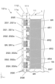
- FIG. 1 is a plan view of a termination circuit board according to a first embodiment of the present disclosure.
- FIG. 7 is a plan view of a modification of the termination circuit board according to the first embodiment of the present disclosure.
- FIG. 7 is a plan view of a termination circuit board according to a second embodiment of the present disclosure.
- FIG. 7 is a plan view of a termination circuit board according to a third embodiment of the present disclosure.
- FIG. 7 is a plan view of a modification of the termination circuit board according to the third embodiment of the present disclosure.
- FIG. 7 is a plan view of a termination circuit board according to a fourth embodiment of the present disclosure.
- FIG. 1 is a perspective view of a termination circuit board according to a first embodiment of the present disclosure.
- 8 is an enlarged plan view of the main part A shown in FIG. 7.
- FIG. 1 is a cross-sectional view of a termination circuit board, an electronic component mounting package, and an electronic module according to a first embodiment of the present disclosure.
- the termination circuit board may be directed either upward or downward, but for convenience, the orthogonal coordinate system xyz is defined and the positive side of the z direction is assumed to be upward.
- the first direction refers to, for example, the x direction in the drawings.
- the second direction intersecting the first direction refers to, for example, the y direction in the drawings.
- plan view is a concept that includes plan view.
- Termination circuit boards 101a to 101d according to the first embodiment of the present disclosure will be described with reference to FIGS. 1, 2, 7, and 8.
- the termination circuit board 101a includes at least a dielectric substrate 1, a ground conductor section 2G, a signal conductor section 3S, a first resistance section 4R, and a second resistance section 5R. .
- Dielectric substrate 1 has a first surface 11 including a first side 11a.
- the material of the dielectric substrate 1 include ceramic materials such as aluminum oxide sintered bodies, mullite sintered bodies, silicon carbide sintered bodies, aluminum nitride sintered bodies, and silicon nitride sintered bodies; Dielectric materials such as glass ceramic materials can be used.
- the dielectric substrate 1 may have a structure in which a plurality of dielectrics are stacked.
- the dielectric substrate 1 is, for example, rectangular in plan view, with a size of 4 mm x 4 mm to 50 mm x 50 mm, and a thickness of 0.5 mm to 10 mm.
- the ground conductor portion 2G is located on the first surface 11, and the distance from the first side 11a in the second direction is the first distance L1.
- the first side 11a and the ground conductor part 2G are located apart, but the first side 11a and the ground conductor part 2G are not necessarily located apart. There's no need to be. That is, the value of the first distance L1 may be zero. The same applies to a second distance L2 and a third distance L3, which will be described later.
- the ground conductor section 2G includes a first ground conductor line 2G1, a second ground conductor line 2G2, a third ground conductor line 2G3, and a fourth ground conductor line 2G4, which are arranged in order in the x direction. ing. More specifically, as shown in FIG. 1, a first ground conductor line 2G1, a second ground conductor line 2G2, a third ground conductor line 2G3, and a fourth ground conductor line 2G4 are lined up in order from the positive side in the x direction. It is located in The first ground conductor line 2G1 and the second ground conductor line 2G2 extend in the y direction and are spaced apart from each other.
- the third ground conductor line 2G3 and the fourth ground conductor line 2G4 extend in the y direction and are spaced apart from each other. Further, the second ground conductor line 2G2 and the third ground conductor line 2G3 extend in the y direction and are located with a gap (fourth distance L4) between them.
- ground conductor portion 2G examples include gold, silver, copper, nickel, tungsten, Metal materials such as molybdenum and manganese may be mentioned.
- the ground conductor portion 2G may be formed by sintering a metal paste on the first surface 11, or may be formed using a thin film forming technique such as a vapor deposition method or a sputtering method.
- An insulating film made of ceramic (for example, alumina coat) or resin may be located on a portion of the ground conductor portion 2G.
- the insulating film can be provided on the ground conductor portion 2G by screen printing. Furthermore, the insulating film may be located only partially on each signal line. With such a configuration, it is possible to reduce the possibility that each signal line is short-circuited.
- the first ground conductor line 2G1, the second ground conductor line 2G2, the third ground conductor line 2G3, and the fourth ground conductor line 2G4 are separated from each other. It is well located. This makes it possible to reduce the possibility that the crosstalk characteristics in the signal conductor section 3S will deteriorate due to the looping of high-frequency signals from the ground conductor section 2G.
- the first ground conductor line 2G1, the second ground conductor line 2G2, the third ground conductor line 2G3, and the fourth ground conductor line 2G4 do not necessarily have to be located separately, and will be described later.
- the connection may be made by an eighth ground conductor line 2G8.
- the signal conductor portion 3S is located on the first surface 11, and the distance from the first side 11a in the y direction is the second distance L2.
- the signal conductor section 3S includes a first signal line 3S1 located between the first ground conductor line 2G1 and the second ground conductor line 2G2, a third ground conductor line 2G3, and a fourth ground conductor line 2G4 in the x direction. and a second signal line 3S2 located between them.
- the material of the signal conductor section 3S may be the same as or different from the material of the ground conductor section 2G, for example, the material of the ground conductor section 2G described above. Similar materials may be mentioned.
- the signal conductor portion 3S may be formed by the same method as the ground conductor portion 2G. Since the first signal line 3S1 is located between the first ground conductor line 2G1 and the second ground conductor line 2G2, the ground potential can be strengthened and the electric field coupling can be strengthened. Therefore, when the first signal line 3S1 transmits a high-frequency signal, it is possible to reduce the possibility that resonance will occur due to the electric field distribution expanding beyond a desired range. Further, by positioning the second signal line 3S2 between the third ground conductor line 2G3 and the fourth ground conductor line 2G4, the same effect as in the above case can be obtained.
- first signal line 3S1 and the second signal line 3S2 may be a pair of differential signal lines that transmit differential signals.
- currents flowing in opposite directions in a pair of signal lines cancel out external noise, making it possible to reduce the effects of EMI noise and allowing smoother transmission of high-frequency signals. be able to.
- the first resistance section 4R is located on the first surface 11 and connects the ground conductor section 2G and the signal conductor section 3S.
- the first resistance section 4R includes a first resistance 4R1, a second resistance 4R2, a third resistance 4R3, and a fourth resistance 4R4.
- the first resistor 4R1 connects the first ground conductor line 2G1 and the first signal line 3S1 in the x direction.
- the second resistor 4R2 connects the second ground conductor line 2G2 and the first signal line 3S1.
- the third resistor 4R3 connects the third ground conductor line 2G3 and the second signal line 3S2.
- the fourth resistor 4R4 connects the fourth ground conductor line 2G4 and the second signal line 3S2.
- the above-mentioned “connected” means physically connected.
- the first resistance part 4R connects the ground conductor part 2G and the signal conductor part 3S means that the first resistance part 4R is in contact with the ground conductor 2G and the signal conductor part 3S, , including a case where a part of the first resistance section 4R is located overlapping the ground conductor 2G and the signal conductor section 3S.
- the first resistor section 4R (first resistor 4R1, second resistor 4R2, third resistor 4R3, fourth resistor 4R4) is formed of a material with higher resistivity than the signal conductor section 3S.
- the material of the first resistive portion 4R include tantalum nitride (TaN or Ta2N), ruthenium oxide (RuO2), nickel chromium alloy (Ni-Cr), copper-nickel alloy (Cu-Ni), or copper-manganese alloy ( Examples include resistor materials such as Cu--Mn).
- the resistor section 4R can be formed on the dielectric substrate 1 (in one embodiment, on the first surface 11) using a thin film formation technique. . Alternatively, it may be formed by a thick film method in which a paste containing powder of a resistor material as a main component is printed and coated on the dielectric substrate 1 and sintered.
- the second resistance portion 5R is located on the first surface 11, and the distance from the first side 11a in the y direction is a third distance L3.
- the second resistance section 5R connects the second ground conductor line 2G2 and the third ground conductor line 2G3 in the x direction.
- the material of the second resistance part 5R may be the same as or different from the material of the first resistance part 4R, and for example, the same material as the material of the first resistance part 4R described above can be mentioned. Further, the second resistance section 5R may be formed on the dielectric substrate 1 by the same method as the first resistance section 4R.
- the termination circuit board 101a includes the second resistance section 5R that connects the second ground conductor line 2G2 and the third ground conductor line 2G3, so that the first signal line Unnecessary electrical signals generated between 3S1 and the second signal line 3S2 can be converted into thermal energy. Therefore, it is possible to reduce the possibility that unnecessary electrical signals will be reflected on the first signal line 3S1 and the second signal line 3S2. This allows the termination circuit board 101a to have improved transmission characteristics and good reflection characteristics even when transmitting high-frequency signals.
- the first resistance section 4R and the second resistance section 5R are thin film resistors. Since the first resistor section 4R and the second resistor section 5R are thin film resistors, the termination circuit board 101a can be made smaller and lower in height. Note that when the first resistance section 4R and the second resistance section 5R are thin film resistors, they are formed on the dielectric substrate 1 (in one embodiment, on the first surface 11) by the above-mentioned thin film formation technique. can do.
- the thin film resistor refers to a resistor having a thickness of 100 um or less, for example. Further, if the first resistance section 4R and the second resistance section 5R are formed of thin films, the dimensional accuracy is excellent, so that the accuracy of the resistance value can be increased.
- the first resistor section 4R and the second resistor section 5R are chip resistors, so the number of components can be reduced on the termination circuit board 101a, and The possibility of deterioration of reflection characteristics can be reduced.
- tantalum nitride (TaN or Ta2N) is used as the main component of the first resistance section 4R and the second resistance section 5R.
- first resistance section 4R and the second resistance section 5R are not limited to those made of a conductor layer as described above, and may be independent components (so-called chip resistors, etc.), and may be made of multiple types. It may also be formed by combining things.
- the "main component" in the present disclosure may be at least a component having the highest content, for example, refers to a component having a content of 90% or more.
- the first surface 11 of the termination circuit board 101a may have a first region 111 and a second region 112, as shown in FIGS. 1 and 8.
- the first region 111 is located apart from the first side 11a and extends in the x direction.
- the second region 112 is located between the first side 11a and the first region 111, and extends in the x direction.
- first resistor 4R1, the second resistor 4R2, the third resistor 4R3, and the fourth resistor 4R4 are located only in the first region 111.
- a fifth distance L5 in the second region 112 between the first signal line 3S1, the first ground conductor line 2G1, and the second ground conductor line 2G2 is the distance L5 between the first signal line 3S1 and the first ground conductor line 2G1.
- it is shorter than the sixth distance L6 in the first region 111 with the second ground conductor line 2G2.
- a first wire 71, a second wire 72, etc. which will be described later, are connected to the first signal line 3S1 in the second region 112, the first signal line 3S1, the first ground conductor line 2G1, and the second ground conductor Since the capacitance component can be increased by being located close to the line 2G2, impedance matching of the first signal line 3S1 can be facilitated. The same applies to the second signal line 3S2.
- Such a termination circuit board 101a has excellent high frequency signal transmission characteristics.
- the first signal line 3S1 includes a first wide portion 3S1b having a larger dimension in the y direction than a portion located in the first region 111 (first narrow portion 3S1c). It may be provided in two areas 112. Similarly, a narrow portion is formed in the first region 111 for each of the second signal line 3S2, the first ground conductor line 2G1, the second ground conductor line 2G2, the third ground conductor line 2G3, and the fourth ground conductor line 2G4. , the second region 112 may have a wide portion. That is, the wide portions located in the second region 112 are located closer to each other in the y direction than the narrow portions located in the first region 111.
- this makes it possible to secure an area for connecting the first wire 71 and the like for connection with the electronic component 104, which will be described later, to the signal conductor section 3S and the ground conductor section 2G. It is possible to easily electrically connect the component 104 and the termination circuit board 101a.
- the first dimension D1 of the first signal line 3S1 and the second signal line 3S2 is as follows: the first ground conductor line 2G1, the second ground conductor line 2G2, the third ground conductor line 2G3,
- the second dimension D2 of the fourth ground conductor line 2G4 may be greater than or equal to the second dimension D2.
- the first dimension D1 of the first signal line 3S1 and the second signal line 3S2 is the first dimension D1 of the first ground conductor line 2G1, the second ground conductor line 2G2, the third ground conductor line 2G3, and the fourth ground conductor line. It is the same as the second dimension D2 of 2G4.
- the first ground conductor line 2G1 has a first end 2G1a
- the second ground conductor line 2G2 has a second end 2G2a
- the third ground conductor line 2G3 has a third end 2G1a
- the fourth ground conductor line 2G4 has a fourth end 2G4a
- the first signal line 3S1 has a fifth end 3S1a
- the second signal line 3S2 has a sixth end 2G3a.
- the second resistance portion 5R has a seventh end portion 5R1a.
- the first end 2G1a, the second end 2G2a, the third end 2G3a, the fourth end 2G4a, the fifth end 3S1a, the sixth end 3S2a, and the seventh end 5R1a are arranged in a straight line (virtually It is located on line C1). With such a configuration, the transmission characteristics of high frequency signals in the first signal line 3S1 and the second signal line 3S2 can be made close to uniform.
- the termination circuit board 101a may further include a third resistance section 6R and a fourth resistance section 7R located on the first surface 11, as shown in FIG.
- the ground conductor section 2G may further include a fifth ground conductor line 2G5 and a sixth ground conductor line 2G6.
- the third resistance section 6R connects the first ground conductor line 2G1 and the fifth ground conductor line 2G5, and the fourth resistance section 7R connects the fourth ground conductor line 2G4 and the sixth ground conductor line 2G6.
- the termination circuit board 101a may include a fifth resistor section 8R located apart from the first signal line 3S1 and the second signal line 3S2.
- the ground conductor section 2G has a seventh ground conductor line 2G7 that is located apart from the first region 111 and extends in the x direction.
- the first surface 11 has the first region 111 and the second region 112, as described above. That is, the first region 111 is located apart from the first side 11a and extends in the x direction.
- the second region 112 is located between the first side 11a and the first region 111, and extends in the x direction.
- the fifth resistance section 8R is connected to the first ground conductor line 2G1, the second ground conductor line 2G2, the third ground conductor line 2G3, and the fourth ground conductor line 2G4, and is also connected to the seventh ground conductor line 2G7. ing. With this configuration, unnecessary electrical signals generated between the first signal line 3S1 and the second signal line 3S2 can be converted into heat energy more efficiently than when the fifth resistor section 8R is not provided. Therefore, it is possible to reduce the possibility that an unnecessary electric signal is reflected to the first signal line 3S1 and the second signal line 3S2.
- the fifth resistance section 8R is located separately from the second resistance section 5R, the third resistance section 6R, and the fourth resistance section 7R, but the fifth resistance section 8R is not necessarily The second resistance section 5R, the third resistance section 6R, and the fourth resistance section 7R do not need to be located separately. That is, the fifth resistance section 8R may be connected to each of the second resistance section 5R, the third resistance section 6R, and the fourth resistance section 7R, or may be connected to any one of them.
- the termination circuit board 101a may further include a first wire 71, a second wire 72, a third wire 73, and a fourth wire 74.
- the first wire 71 and the second wire 72 electrically connect the first signal line 3S1 and the electronic component 104.
- the third wire 73 and the fourth wire 74 electrically connect the second signal line 3S2 and the electronic component 104.
- the distance L712 between the first wire 71 and the second wire 72 in the x direction becomes smaller toward the outside along the y direction (in the negative direction of the y axis in one embodiment).
- the distance L734 between the third wire 73 and the fourth wire 74 in the x direction becomes smaller toward the outside along the y direction (the negative direction of the y axis).
- the distance in the x direction between the first wire 71 and the second wire 72 at the location connected to the first signal line 3S1 is L712a
- the distance between the first wire 71 and the second wire 72 at the location connected to the electronic component 104 is L712a.
- L712a the distance between the first wire 71 and the second wire 72 in the x direction
- L712a the distance between the third wire 73 and the fourth wire 74 at the location connected to the second signal line 3S2
- the distance between the third wire 73 and the fourth wire 74 at the location connected to the electronic component 104 is set to L734a.
- the first wire 71 and the second wire 72 electrically connect the first signal line 3S1 and the seventh signal line 104S7 of the electronic component 104.
- the third wire 73 and the fourth wire 74 electrically connect the second signal line 3S2 and the eighth signal line 104S8 of the electronic component 104. Connected.
- the absolute value of the inclination of the first wire 71 in the x direction may be the same as the absolute value of the inclination of the second wire 72 in the x direction in plan view. That is, the inclination of the first wire 71 in the x direction is symmetrical with the inclination of the second wire 72 in the x direction with the first signal line 3S1 in between.
- the third wire 73 and the fourth wire 74 also have the same configuration as the first wire 71 and the second wire 72 described above.
- the termination circuit board 101a may include one or more fifth wires 75 and one or more sixth wires 76.
- the fifth wire 75 is located further away from the second wire 72 than the first wire 71 and connects the first ground conductor line 2G1 and the tenth ground conductor line 104G of the electronic component 104.
- the sixth wire 76 is located further away from the first wire 72 than the second wire 71, and connects the second ground conductor line 2G2 and the tenth ground conductor line 104G.
- the inclination of the fifth wire 75 in the x direction is the same as the inclination of the first wire 71 in the x direction.
- the inclination of the sixth wire 76 with respect to the x direction is the same as the inclination of the second wire 72 with respect to the x direction. Note that the positional relationships among the first wire 71, second wire 72, third wire 73, fourth wire 74, fifth wire 75, and sixth wire 76 are not limited to those in the above embodiment.
- Examples of the material of the first wire 71 include a conductive metal material such as platinum.
- the second wire 72, the third wire 73, the fourth wire 74, the fifth wire 75, and the sixth wire 76 may also be made of the same material as the first wire 71, or may be made of different materials.
- the termination circuit board 101b according to the second embodiment differs from the first embodiment in that the second ground conductor line 2G2 and the third ground conductor line 2G3 are located apart.
- the second ground conductor line 2G2 and the third ground conductor line 2G3 are located apart from each other, which means that the second ground conductor line 2G2 and the third ground conductor line 2G3 are located separately from each other. , and are not electrically connected to each other on the termination circuit board 101b. That is, in one embodiment, the second resistance portion 5R in the first embodiment described above is not provided between the second ground conductor line 2G2 and the third ground conductor line 2G3. As a result, it is not necessary to provide the second resistor section 5R, so that the number of steps in manufacturing the termination circuit board 101b can be reduced.
- the termination circuit board 101c according to the third embodiment is different from the first embodiment in that it further includes a fifth resistance section 8R, a seventh ground conductor line 2G7, and an eighth ground conductor line 2G8. different. That is, as shown in FIG. 4, the termination circuit board 101c may further include a fifth resistor section 8R located apart from the first signal line 3S1 and the second signal line 3S2.
- the ground conductor section 2G includes a seventh ground conductor line 2G7 and an eighth ground conductor line 2G8.
- the seventh ground conductor line 2G7 is located apart from the first region 111 and extends in the x direction.
- the eighth ground conductor line 2G8 is located between the seventh ground conductor line 2G7 and the first region 111, and extends in the x direction. Further, the eighth ground conductor line 2G8 is connected to the first ground conductor line 2G1, the second ground conductor line 2G2, the third ground conductor line 2G3, and the fourth ground conductor line 2G4.
- the fifth resistance section 8R is connected to the seventh ground conductor line 2G7 and the eighth ground conductor line 2G8.
- the first signal line 3S1 is surrounded by the first ground conductor line 2G1, the second ground conductor line 2G2, and the eighth ground conductor line 2G8, and the second signal line 3S2 is surrounded by the third ground conductor line 2G3, It is surrounded by a fourth ground conductor line 2G4 and an eighth ground conductor line 2G8.
- a plurality of fifth resistance portions 8R may be located between the seventh ground conductor line 2G7 and the eighth ground conductor line 2G8. More specifically, as shown in FIG. 5, the fifth resistance section 8R may include a sixth resistance section 8R6, a seventh resistance section 8R7, and an eighth resistance section 8R8.
- the sixth resistance section 8R6 is connected to the third resistance section 6R
- the seventh resistance section 8R7 is connected to the second resistance section 5R
- the eighth resistance section 8R8 is connected to the fourth resistance section 7R from the y direction. When viewed from the side, they are located overlapping each other.
- the first signal line 3S1 includes a third signal line 3S13 and a fourth signal line 3S14 spaced apart from the third signal line 3S13.
- the second signal line 3S2 includes a fifth signal line 3S25 and a sixth signal line 3S26 spaced apart from the fifth signal line 3S25.
- the first resistance section 4R further includes a fifth resistance 4R5, a sixth resistance 4R6, a seventh resistance 4R7, and an eighth resistance 4R8.
- the fifth resistor 4R5 is located overlapping the third signal line 3S13
- the sixth resistor 4R6 is located overlapping the fourth signal line 3S14
- the seventh resistor 4R7 is located overlapping the fourth signal line 3S14.
- the eighth resistor 4R8 is located overlapping with the sixth signal line 3S26.
- the first resistor 4R1 and the fifth resistor 4R5 connect the third signal line 3S13 and the first ground conductor line 2G1.
- the second resistor 4R2 and the sixth resistor 4R6 connect the fourth signal line 3S14 and the second ground conductor line 2G2.
- the third resistor 4R3 and the seventh resistor 4R7 connect the fifth signal line 3S25 and the third ground conductor line 2G3.
- the fourth resistor 4R4 and the eighth resistor 4R8 connect the sixth signal line 3S26 and the fourth ground conductor line 2G4.
- the third signal line 3S13 and the fourth signal line 3S14 are a pair of signal lines that transmit differential signals.
- the fifth signal line 3S25 and the sixth signal line 3S26 are a pair of signal lines that transmit differential signals of channels different from the first signal line 3S1 (the third signal line 3S13 and the fourth signal line 3S14). be.
- unnecessary electrical signals generated between the first signal line 3S1 and the second signal line 3S2 and between the fifth signal line 3S25 and the sixth signal line 3S26 are converted into thermal energy. , can be changed more efficiently, so it is possible to reduce the possibility that unnecessary electrical signals will be reflected to the first signal line 3S1 and the second signal line 3S2.
- FIG. 9 is a cross-sectional view of the electronic module 10 including the electronic component mounting package 100 and equipped with the termination circuit board 101a according to the first embodiment.
- the electronic component mounting package 100 includes a terminal circuit board 101a, a base 102, and a frame 103.
- the frame 103 is joined to the upper surface of the base 102, and the terminal circuit board 101a is fixed to the frame 103.
- the termination circuit board 101a may be bonded to the upper surface of the base 102.
- the base 102 has an upper surface.
- the base 102 has a rectangular shape in a plan view, and has a size of 10 mm x 10 mm to 50 mm x 50 mm, and a thickness of 0.5 mm to 20 mm.
- the material of the base 102 include metal materials such as copper, iron, tungsten, molybdenum, nickel, or cobalt, or alloys containing these metal materials.
- the base 102 may be a single metal plate or a laminate formed by laminating a plurality of metal plates.
- the material of the base 102 is the above-mentioned metal material
- the surface of the base 102 is plated with nickel or gold using an electroplating method or an electroless plating method in order to reduce oxidation corrosion.
- a layer may be formed.
- the material of the base 102 is an insulating material, such as an aluminum oxide sintered body, a mullite sintered body, a silicon carbide sintered body, an aluminum nitride sintered body, a silicon nitride sintered body, or It may also be a ceramic material such as glass ceramics.
- the base 102 may have a first pedestal 102a and a second pedestal 102b for mounting the electronic component 104.
- the termination circuit board 101a may be mounted on the second pedestal portion 102b.
- the frame 103 is located on the upper surface of the base 102 and protects the electronic component 104 located inside when viewed from above. That is, in plan view, the frame 103 is located so as to surround the electronic component 104.
- the frame 103 may include a wiring base 103a for communicating signals with the outside and a frame 103b. That is, the outer edge of the upper surface of the base 102 is surrounded by the wiring base 103a and the frame 103b. That is, the wiring base portion 103a and the frame portion 103b are located so as to surround the electronic component 104.
- the frame 103 is located along the outer edge of the upper surface of the base 102, but the frame 103 may be located inside the outer edge of the upper surface of the base 102.
- the material of the frame 103 may be, for example, a metal material such as copper, iron, tungsten, molybdenum, nickel, or cobalt, or an alloy containing these metal materials.
- the material of the frame 103 is an insulating material, such as an aluminum oxide sintered body, a mullite sintered body, a silicon carbide sintered body, an aluminum nitride sintered body, or a silicon nitride sintered body.
- it may be a ceramic material such as glass ceramics.
- the material of the wiring base 103a may be, for example, an aluminum oxide sintered body, a mullite sintered body, a silicon carbide sintered body, or an aluminum nitride sintered body. Ceramic materials such as solid bodies or silicon nitride sintered bodies, and dielectric materials such as glass ceramic materials can be used.
- the wiring base portion 103a may have a structure in which a plurality of insulating layers are stacked. Furthermore, the wiring base portion 103a and the frame portion 103b may be made of the same or different materials.
- wiring is formed using a metal material such as gold, silver, copper, nickel, tungsten, molybdenum, and manganese on a green sheet that forms the outer shape of the wiring base 103a. may be formed. Further, the wiring may be formed by sintering a metal paste, or may be formed using a thin film forming technique such as a vapor deposition method or a sputtering method. An insulating film made of ceramic (for example, alumina coat) or resin may be located on a portion of the wiring.
- the frame 103 can be joined to the base 102 via a brazing material or the like.
- the material of the brazing material is, for example, silver, copper, gold, aluminum, or magnesium, and may contain additives such as nickel, cadmium, or phosphorus.
- the electronic module 10 includes an electronic component mounting package 100, an electronic component 104, and a lid 106. Further, the electronic module 10 may include a seal ring 105.
- the electronic component 104 may be a component that processes signals, such as converting an optical signal into an electrical signal or converting an electrical signal into an optical signal.
- the electronic component 104 is located on the upper surface of the base 102 and is housed in the electronic component mounting package 100.
- Examples of the electronic component 104 include a semiconductor laser (LD) or an optical semiconductor element such as a photodiode (PD), a semiconductor integrated circuit element, and a sensor element such as an optical sensor.
- Electronic component 104 can be formed from a semiconductor material, such as gallium arsenide or gallium nitride.
- the electronic component 104 may include a thin film resistor.
- the thin film resistor may be provided in the same configuration as the termination circuit board 101a.
- the electronic component 104 may be mounted directly on the base 102, or may be mounted via the first pedestal 102a as described above.
- the lid 106 is positioned on the frame 103 to cover the inside of the electronic component mounting package 100, and protects the electronic component 104 together with the frame 103.
- the lid body 106 has a rectangular shape in a plan view, and has a size of 10 mm x 10 mm to 50 mm x 50 mm, and a thickness of 0.5 mm to 2 mm.
- the material of the lid body 106 include metal materials such as iron, copper, nickel, chromium, cobalt, molybdenum, or tungsten, or alloys made by combining a plurality of these metal materials.
- the metal member constituting the lid body 106 can be manufactured by subjecting an ingot of such a metal material to a metal processing method such as a rolling method or a punching method.
- the seal ring 105 has the function of joining the lid 106 and the frame 103.
- the seal ring 105 is located on the frame 103 and surrounds the electronic component 104 in plan view.
- Examples of the material for the seal ring 105 include metal materials such as iron, copper, silver, nickel, chromium, cobalt, molybdenum, or tungsten, or alloys made by combining multiple of these metal materials. Note that when the seal ring 105 is not provided on the frame body 103, the lid body 106 may be bonded via a bonding material such as solder, brazing material, glass, or resin adhesive, for example.
- the present disclosure can be used as a termination circuit board, a package for mounting electronic components, and an electronic module.
- Dielectric substrate 11 First surface 11a First side 111 First region 112 Second region 2G Ground conductor section 2G1 First ground conductor line 2G1a First end 2G2 Second ground conductor line 2G2a Second end 2G3 Third ground Conductor line 2G3a Second end 2G4 Fourth ground conductor line 2G4a Second end 2G5 Fifth ground conductor line 2G6 Sixth ground conductor line 2G7 Seventh ground conductor line 2G8 Eighth ground conductor line 3S Signal conductor part 3S1 First signal Line 3S1a Fifth end 3S1b First wide portion 3S1c First narrow portion 3S13 Third signal line 3S14 Fourth signal line 3S2 Second signal line 3S2a Sixth end 3S25 Fifth signal line 3S26 Sixth signal line 4R First Resistor part 4R1 First resistor 4R2 Second resistor 4R3 Third resistor 4R4 Fourth resistor 4R5 Fifth resistor 4R6 Sixth resistor 4R7 Seventh resistor 4R8 Eighth resistor 5R Second resistor part 5R1a Seven
Landscapes
- Structure Of Printed Boards (AREA)
Priority Applications (2)
| Application Number | Priority Date | Filing Date | Title |
|---|---|---|---|
| EP23816063.4A EP4535553A1 (en) | 2022-06-01 | 2023-05-30 | Termination circuit substrate, package for mounting electronic component, and electronic module |
| JP2024524879A JP7728456B2 (ja) | 2022-06-01 | 2023-05-30 | 終端回路基板、電子部品実装用パッケージ、および電子モジュール |
Applications Claiming Priority (2)
| Application Number | Priority Date | Filing Date | Title |
|---|---|---|---|
| JP2022-089677 | 2022-06-01 | ||
| JP2022089677 | 2022-06-01 |
Publications (1)
| Publication Number | Publication Date |
|---|---|
| WO2023234306A1 true WO2023234306A1 (ja) | 2023-12-07 |
Family
ID=89024877
Family Applications (1)
| Application Number | Title | Priority Date | Filing Date |
|---|---|---|---|
| PCT/JP2023/020127 Ceased WO2023234306A1 (ja) | 2022-06-01 | 2023-05-30 | 終端回路基板、電子部品実装用パッケージ、および電子モジュール |
Country Status (3)
| Country | Link |
|---|---|
| EP (1) | EP4535553A1 (https=) |
| JP (1) | JP7728456B2 (https=) |
| WO (1) | WO2023234306A1 (https=) |
Citations (4)
| Publication number | Priority date | Publication date | Assignee | Title |
|---|---|---|---|---|
| US20050128022A1 (en) * | 2003-10-27 | 2005-06-16 | Markus Ulm | Structural element having a coplanar line |
| JP2008085699A (ja) * | 2006-09-28 | 2008-04-10 | Kyocera Corp | 高周波用終端抵抗基板および電子装置 |
| JP2010135712A (ja) | 2008-10-29 | 2010-06-17 | Kyocera Corp | 配線基板および半導体素子収納用パッケージならびに半導体装置 |
| KR101462391B1 (ko) * | 2013-06-18 | 2014-11-17 | 전자부품연구원 | 터미네이션부를 포함하는 알에프 소자 |
-
2023
- 2023-05-30 EP EP23816063.4A patent/EP4535553A1/en not_active Withdrawn
- 2023-05-30 JP JP2024524879A patent/JP7728456B2/ja active Active
- 2023-05-30 WO PCT/JP2023/020127 patent/WO2023234306A1/ja not_active Ceased
Patent Citations (4)
| Publication number | Priority date | Publication date | Assignee | Title |
|---|---|---|---|---|
| US20050128022A1 (en) * | 2003-10-27 | 2005-06-16 | Markus Ulm | Structural element having a coplanar line |
| JP2008085699A (ja) * | 2006-09-28 | 2008-04-10 | Kyocera Corp | 高周波用終端抵抗基板および電子装置 |
| JP2010135712A (ja) | 2008-10-29 | 2010-06-17 | Kyocera Corp | 配線基板および半導体素子収納用パッケージならびに半導体装置 |
| KR101462391B1 (ko) * | 2013-06-18 | 2014-11-17 | 전자부품연구원 | 터미네이션부를 포함하는 알에프 소자 |
Also Published As
| Publication number | Publication date |
|---|---|
| JP7728456B2 (ja) | 2025-08-22 |
| JPWO2023234306A1 (https=) | 2023-12-07 |
| EP4535553A1 (en) | 2025-04-09 |
Similar Documents
| Publication | Publication Date | Title |
|---|---|---|
| US20040080917A1 (en) | Integrated microwave package and the process for making the same | |
| US20250056726A1 (en) | Wiring board, electronic component mounting package using wiring board, and electronic module | |
| JP2000357960A (ja) | 高密度を有するボールグリッドアレイrcネットワーク | |
| US6936921B2 (en) | High-frequency package | |
| JP7728456B2 (ja) | 終端回路基板、電子部品実装用パッケージ、および電子モジュール | |
| JP3878795B2 (ja) | 多層配線基板 | |
| US20250351264A1 (en) | Wiring board, electronic component mounting package using wiring board, and electronic module | |
| US20240243055A1 (en) | Electronic-component mounting package and electronic device | |
| JP4009169B2 (ja) | 半導体素子収納用パッケージおよび半導体装置 | |
| JP3798978B2 (ja) | 多層配線基板 | |
| JPH0613490A (ja) | 半導体装置 | |
| JP7784549B2 (ja) | 配線構造体および電子モジュール | |
| WO2024029628A1 (ja) | 配線基板、配線基板を用いた電子部品実装用パッケージおよび電子モジュール | |
| JP7817435B2 (ja) | 配線基板、配線基板を用いた電子部品実装用パッケージ、および電子モジュール | |
| JP2024072552A (ja) | 薄膜回路基板、電子部品実装用パッケージ、および電子モジュール | |
| JPH11339898A (ja) | 高周波用入出力端子および高周波回路用パッケージ | |
| JP7716590B2 (ja) | 導波管変換器、電子部品実装用パッケージ、および導波管変換装置 | |
| US20240105600A1 (en) | Wiring substrate, wiring structure using wiring substrate, electronic component mounting package, and electronic module | |
| JP2020017622A (ja) | 配線基板、電子部品用パッケージおよび電子装置 | |
| JP2000277656A (ja) | 多層配線基板 | |
| JP3792482B2 (ja) | 多層配線基板 | |
| JP2024104570A (ja) | 配線構造体、配線構造体を用いた電子部品実装用パッケージ、および電子モジュール | |
| JP4614788B2 (ja) | 配線基板 | |
| JP2001127385A (ja) | 多層配線基板 | |
| JPH10135637A (ja) | セラミック多層配線基板 |
Legal Events
| Date | Code | Title | Description |
|---|---|---|---|
| 121 | Ep: the epo has been informed by wipo that ep was designated in this application |
Ref document number: 23816063 Country of ref document: EP Kind code of ref document: A1 |
|
| WWE | Wipo information: entry into national phase |
Ref document number: 2024524879 Country of ref document: JP |
|
| WWE | Wipo information: entry into national phase |
Ref document number: 2023816063 Country of ref document: EP |
|
| NENP | Non-entry into the national phase |
Ref country code: DE |
|
| ENP | Entry into the national phase |
Ref document number: 2023816063 Country of ref document: EP Effective date: 20250102 |
|
| WWP | Wipo information: published in national office |
Ref document number: 2023816063 Country of ref document: EP |
|
| WWW | Wipo information: withdrawn in national office |
Ref document number: 2023816063 Country of ref document: EP |