EP4535553A1 - Termination circuit substrate, package for mounting electronic component, and electronic module - Google Patents
Termination circuit substrate, package for mounting electronic component, and electronic module Download PDFInfo
- Publication number
- EP4535553A1 EP4535553A1 EP23816063.4A EP23816063A EP4535553A1 EP 4535553 A1 EP4535553 A1 EP 4535553A1 EP 23816063 A EP23816063 A EP 23816063A EP 4535553 A1 EP4535553 A1 EP 4535553A1
- Authority
- EP
- European Patent Office
- Prior art keywords
- ground conductor
- line
- resistor
- conductor line
- signal line
- Prior art date
- Legal status (The legal status is an assumption and is not a legal conclusion. Google has not performed a legal analysis and makes no representation as to the accuracy of the status listed.)
- Withdrawn
Links
Images


Classifications
-
- H—ELECTRICITY
- H01—ELECTRIC ELEMENTS
- H01P—WAVEGUIDES; RESONATORS, LINES, OR OTHER DEVICES OF THE WAVEGUIDE TYPE
- H01P1/00—Auxiliary devices
- H01P1/24—Terminating devices
- H01P1/26—Dissipative terminations
- H01P1/268—Strip line terminations
-
- H—ELECTRICITY
- H01—ELECTRIC ELEMENTS
- H01S—DEVICES USING THE PROCESS OF LIGHT AMPLIFICATION BY STIMULATED EMISSION OF RADIATION [LASER] TO AMPLIFY OR GENERATE LIGHT; DEVICES USING STIMULATED EMISSION OF ELECTROMAGNETIC RADIATION IN WAVE RANGES OTHER THAN OPTICAL
- H01S5/00—Semiconductor lasers
- H01S5/02—Structural details or components not essential to laser action
- H01S5/022—Mountings; Housings
- H01S5/02208—Mountings; Housings characterised by the shape of the housings
- H01S5/02216—Butterfly-type, i.e. with electrode pins extending horizontally from the housings
-
- H—ELECTRICITY
- H01—ELECTRIC ELEMENTS
- H01S—DEVICES USING THE PROCESS OF LIGHT AMPLIFICATION BY STIMULATED EMISSION OF RADIATION [LASER] TO AMPLIFY OR GENERATE LIGHT; DEVICES USING STIMULATED EMISSION OF ELECTROMAGNETIC RADIATION IN WAVE RANGES OTHER THAN OPTICAL
- H01S5/00—Semiconductor lasers
- H01S5/02—Structural details or components not essential to laser action
- H01S5/022—Mountings; Housings
- H01S5/0233—Mounting configuration of laser chips
- H01S5/02345—Wire-bonding
-
- H—ELECTRICITY
- H01—ELECTRIC ELEMENTS
- H01S—DEVICES USING THE PROCESS OF LIGHT AMPLIFICATION BY STIMULATED EMISSION OF RADIATION [LASER] TO AMPLIFY OR GENERATE LIGHT; DEVICES USING STIMULATED EMISSION OF ELECTROMAGNETIC RADIATION IN WAVE RANGES OTHER THAN OPTICAL
- H01S5/00—Semiconductor lasers
- H01S5/06—Arrangements for controlling the laser output parameters, e.g. by operating on the active medium
- H01S5/062—Arrangements for controlling the laser output parameters, e.g. by operating on the active medium by varying the potential of the electrodes
- H01S5/06226—Modulation at ultra-high frequencies
Definitions
- the present disclosure relates to a termination circuit board, an electronic component mounting package, and an electronic module.
- a semiconductor element accommodating package that accommodates a semiconductor element utilizes a wiring board that is coupled to the semiconductor element.
- the semiconductor element processes an electrical signal (for example, a radio-frequency signal).
- a known example of the wiring board is a wiring board described in Patent Literature 1.
- the wiring board described in Patent Literature 1 includes a resistor to convert a signal including a radio-frequency signal component from electrical energy to thermal energy to reduce noise due to reflection of the signal.
- the wiring board described in Patent Literature 1 includes a signal line conductor on a dielectric substrate, a first ground conductor disposed on both sides of the signal line conductor with a gap between the first ground conductor and the signal line, and a resistor coupling one end of the signal line conductor and the first ground conductor.
- Patent Literature 1 Japanese Unexamined Patent Application Publication No. 2010-135712
- the first resistor part includes a first resistor that couples the first ground conductor line to the first signal line in the first direction, a second resistor that couples the second ground conductor line to the first signal line in the first direction, a third resistor that couples the third ground conductor line to the second signal line in the first direction, and a fourth resistor that couples the fourth ground conductor line to the second signal line in the first direction.
- the second resistor part couples the second ground conductor line to the third ground conductor line in the first direction.
- any direction may be defined as an upper direction or a lower direction regarding a termination circuit board.
- an orthogonal coordinate system xyz is defined, and a positive side in a z-direction is assumed as the upper direction.
- a first direction indicates, for example, an x-direction in the drawings.
- a second direction intersecting with the first direction indicates, for example, a y-direction in the drawings.
- plan view is a concept including planar transparent view.
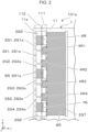
- termination circuit boards 101a to 101d are described with reference to FIGs. 1 , 2 , 7 , and 8 .
- the termination circuit board 101a at least includes a dielectric substrate 1, a ground conductor part 2G, a signal conductor part 3S, a first resistor part 4R, and a second resistor part 5R.
- the dielectric substrate 1 may include a configuration in which multiple dielectrics are laminated on one another.
- the dielectric substrate 1 has a rectangular shape in plan view, a size of 4 mm ⁇ 4 mm to 50 mm ⁇ 50 mm, and a thickness of 0.5 mm to 10 mm.
- the ground conductor part 2G is positioned on the first surface 11, and a distance in the second direction between the ground conductor part 2G and the first side 11a is a first distance L1.
- the first side 11a and the ground conductor part 2G are positioned apart from one another.
- the first side 11a and the ground conductor part 2G are not necessarily positioned apart from one another. That is, a value of the first distance L1 may be zero.
- the same and/or similar also applies to a second distance L2 and a third distance L3 which will be described later.
- the ground conductor part 2G, the signal conductor part 3S, the first resistor part 4R, and the second resistor part 5R can have less possibility of getting damaged when the dielectric substrate 1 to be the termination circuit board 101a is manufactured by dicing.
- the third ground conductor line 2G3 and the fourth ground conductor line 2G4 extend in the y-direction and are positioned with a gap therebetween.
- the second ground conductor line 2G2 and the third ground conductor line 2G3 extend in the y-direction and are positioned with a gap (fourth distance L4) therebetween.
- Examples of a material for the ground conductor part 2G include a metal material, such as gold, silver, copper, nickel, tungsten, molybdenum, or manganese.
- the ground conductor part 2G may be formed by sintering of metal paste on the first surface 11, or formed by using a thin-film formation technology, such as a vapor deposition method or a spattering method.
- An insulating film such as a ceramic (for example, aluminum coat) or a resin may be positioned on a portion of the ground conductor part 2G.
- the insulating film can be provided onto the ground conductor part 2G by screen printing.
- the insulating film may be positioned only on a portion of each signal line. Such a configuration can lower possibility of short-circuiting in each signal line.
- a material for the signal conductor part 3S may be the same as or different from the material for the ground conductor part 2G, and be, for example, a material the same as and/or similar to the material for the ground conductor part 2G described above.
- the signal conductor part 3S may be formed in a method the same as and/or similar to that for the ground conductor part 2G. Positioning of the first signal line 3S1 between the first ground conductor line 2G1 and the second ground conductor line 2G2 can reinforce ground potential and strengthen electric-field coupling. Therefore, the first signal line 3S1 can have less possibility of occurrence of resonance that occurs due to spreading of electric field distribution beyond an intended range during transmission of a radio-frequency signal. Positioning of the second signal line 3S2 between the third ground conductor line 2G3 and the fourth ground conductor line 2G4 can achieve an effect as that of the case described above.
- the first resistor part 4R is positioned on the first surface 11 and couples the ground conductor part 2G to the signal conductor part 3S.
- the first resistor part 4R includes a first resistor 4R1, a second resistor 4R2, a third resistor 4R3, and a fourth resistor 4R4.
- the first resistor 4R1 couples the first ground conductor line 2G1 to the first signal line 3S1 in the x-direction.
- the second resistor 4R2 couples the second ground conductor line 2G2 to the first signal line 3S1.
- the third resistor 4R3 couples the third ground conductor line 2G3 to the second signal line 3S2.
- the fourth resistor 4R4 couples the fourth ground conductor line 2G4 to the second signal line 3S2.
- the first resistor part 4R (the first resistor 4R1, the second resistor 4R2, the third resistor 4R3, and the fourth resistor 4R4) is made of a material with higher resistivity than that of the signal conductor part 3S.
- the material for the first resistor part 4R include a resistor material, such as tantalum nitride (TaN or Ta2N), ruthenium oxide (RuO2), nickel-chrome alloy (Ni-Cr), copper-nickel alloy (Cu-Ni), or copper-manganese alloy (Cu-Mn).
- the first resistor part 4R and the second resistor part 5R are made of thin films, the first resistor part 4R and the second resistor part 5R are excellent in precision of dimension, and thus can have improved precision of a resistance value. As compared with a case in which the first resistor part 4R and the second resistor part 5R are chip resistors, mounting of the chip resistors is unnecessary, and thereby the termination circuit board 101a can have a reduced number of components and reduced possibility of deterioration in reflection characteristics due to the chip resistor mounting part.
- the termination circuit board 101a may include the first surface 11 including a first region 111 and a second region 112.
- the first region 111 is positioned with a gap between the first region 111 and the first side 11a and extends in the x-direction.
- the second region 112 is positioned between the first side 11a and the first region 111 and extends in the x-direction.
- the first signal line 3S1, the second signal line 3S2, the first ground conductor line 2G1, the second ground conductor line 2G2, the third ground conductor line 2G3, and the fourth ground conductor line 2G4 extend from the second region 112 to the first region 111 in the y-direction intersecting with the x-direction.
- the first dimension D1 of each of the first signal line 3S1 and the second signal line 3S2 is the same as the second dimension D2 of each of the first ground conductor line 2G1, the second ground conductor line 2G2, the third ground conductor line 2G3, and the fourth ground conductor line 2G4.
- the first ground conductor line 2G1 includes a first end part 2G1a
- the second ground conductor line 2G2 includes a second end part 2G2a
- the third ground conductor line 2G3 includes a third end part 2G3a
- the fourth ground conductor line 2G4 includes a fourth end part 2G4a
- the first signal line 3S1 includes a fifth end part 3S1a
- the second signal line 3S2 includes a sixth end part 3S2a
- the second resistor part 5R includes a seventh end part 5R1a.
- the ground conductor part 2G, the signal conductor part 3S, the first resistor part 4R, and the second resistor part 5R can have less possibility of getting damaged when the dielectric substrate 1 to be the termination circuit board 101a is manufactured by dicing.
- the second region 112 is positioned between the first side 11a and the first region 111 and extends in the x-direction.
- the fifth resistor part 8R is coupled to the first ground conductor line 2G1, the second ground conductor line 2G2, the third ground conductor line 2G3, and fourth ground conductor line 2G4, as well as to the seventh ground conductor line 2G7.
- the fifth resistor part 8R is positioned to separate from the second resistor part 5R, the third resistor part 6R, and the fourth resistor part 7R.
- the fifth resistor part 8R is not necessarily positioned to separate from the second resistor part 5R, the third resistor part 6R, and the fourth resistor part 7R. That is, the fifth resistor part 8R may be coupled to each of the second resistor part 5R, the third resistor part 6R, and the fourth resistor part 7R, or may be coupled to any one of them.
- the termination circuit board 101a may further include the first wire 71, the second wire 72, a third wire 73, and a fourth wire 74.
- the first wire 71 and the second wire 72 electrically couple the first signal line 3S1 to the electronic component 104.
- the third wire 73 and the fourth wire 74 electrically couple the second signal line 3S2 to the electronic component 104.
- a distance L712 in the x-direction between the first wire 71 and the second wire 72 decreases outwardly in the y-direction (in an embodiment, in the negative direction of the y-axis).
- the first wire 71 and the second wire 72 electrically couple the first signal line 3S1 to a seventh signal line 104S7 of the electronic component 104.
- the third wire 73 and the fourth wire 74 electrically couple the second signal line 3S2 to an eighth signal line 104S8 of the electronic component 104.
- the termination circuit board 101b is different from the first embodiment in that the second ground conductor line 2G2 and the third ground conductor line 2G3 are positioned apart from one another.
- the second ground conductor line 2G2 and the third ground conductor line 2G3 being positioned apart from one another means the second ground conductor line 2G2 and the third ground conductor line 2G3 being positioned to separate from one another, and not being even electrically coupled to one another on the termination circuit board 101b. That is, an embodiment does not include the second resistor part 5R of the first embodiment between the second ground conductor line 2G2 and the third ground conductor line 2G3. Therefore, providing of the second resistor part 5R is unnecessary, and thus manufacturing of the termination circuit board 101b can require reduced man-hours.
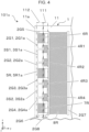
- the termination circuit board 101c is described with reference to FIGs. 4 and 5 . Note that, below, only a configuration of the third embodiment different from the configuration of the first embodiment is described, and the other configurations are denoted by the same reference signs as those in the first embodiment to omit description.
- the termination circuit board 101c is different from the first embodiment in that the termination circuit board 101c further includes the fifth resistor part 8R, the seventh ground conductor line 2G7, and the eighth ground conductor line 2G8.
- the termination circuit board 101c may further include the fifth resistor part 8R positioned with a gap between the fifth resistor part 8R and each of the first signal line 3S1 and the second signal line 3S2.
- the ground conductor part 2G includes the seventh ground conductor line 2G7 and the eighth ground conductor line 2G8.
- the seventh ground conductor line 2G7 is positioned with a gap between the seventh ground conductor line 2G7 and the first region 111 and extends in the x-direction.
- the eighth ground conductor line 2G8 is positioned between the seventh ground conductor line 2G7 and the first region 111 and extends in the x-direction.
- the eighth ground conductor line 2G8 is coupled to the first ground conductor line 2G1, the second ground conductor line 2G2, the third ground conductor line 2G3, and the fourth ground conductor line 2G4.
- the fifth resistor part 8R is coupled to the seventh ground conductor line 2G7 and the eighth ground conductor line 2G8.
- the first signal line 3S1 is surrounded by the first ground conductor line 2G1, the second ground conductor line 2G2, and the eighth ground conductor line 2G8.
- the second signal line 3S2 is surrounded by the third ground conductor line 2G3, the fourth ground conductor line 2G4, and the eighth ground conductor line 2G8.
- an unnecessary electrical signal generated between the first signal line 3S1 and the second signal line 3S2 is more efficiently convertible to thermal energy. Accordingly, an unnecessary electrical signal can have less possibility of reflecting toward the first signal line 3S1 and the second signal line 3S2.
- the fifth resistor part 8R may include a plurality of resistor parts positioned between the seventh ground conductor line 2G7 and the eighth ground conductor line 2G8. More specifically, as illustrated in FIG. 5 , the fifth resistor part 8R may include a sixth resistor part 8R6, a seventh resistor part 8R7, and an eighth resistor part 8R8. Further, in an embodiment, the sixth resistor part 8R6 may overlap the third resistor part 6R, the seventh resistor part 8R7 may overlap the second resistor part 5R, and the eighth resistor part 8R8 may overlap the fourth resistor part 7R in side view in the y-direction.
- the termination circuit board 101d is described with reference to FIG. 6 . Note that, below, only a configuration of the fourth embodiment different from the configuration of the first embodiment is described, and the other configurations are denoted by the same reference signs as those in the first embodiment to omit description.
- the first signal line 3S1 includes a third signal line 3S13, and a fourth signal line 3S14 positioned with a gap between the fourth signal line 3S14 and the third signal line 3S13.
- the second signal line 3S2 includes a fifth signal line 3S25, and a sixth signal line 3S26 positioned with a gap between the sixth signal line 3S26 and the fifth signal line 3S25.
- the first resistor part 4R further includes a fifth resistor 4R5, a sixth resistor 4R6, a seventh resistor 4R7, and an eighth resistor 4R8.
- the first resistor 4R1 and the fifth resistor 4R5 couple the third signal line 3S13 to the first ground conductor line 2G1.
- the second resistor 4R2 and the sixth resistor 4R6 couple the fourth signal line 3S14 to the second ground conductor line 2G2.
- the third resistor 4R3 and the seventh resistor 4R7 couple the fifth signal line 3S25 to the third ground conductor line 2G3.
- the fourth resistor 4R4 and the eighth resistor 4R8 couple the sixth signal line 3S26 to the fourth ground conductor line 2G4.
- the third signal line 3S13 and the fourth signal line 3S14 are a pair of signal lines that transmit differential signals.
- the fifth signal line 3S25 and the sixth signal line 3S26 are a pair of signal lines that transmit differential signals on a channel different from a channel of the first signal line 3S1 (the third signal line 3S13 and the fourth signal line 3S14).
- unnecessary electrical signals generated between the first signal line 3S1 and the second signal line 3S2 and between the fifth signal line 3S25 and the sixth signal line 3S26 are more efficiently convertible to thermal energy. Accordingly, unnecessary electrical signals can have less possibility of reflecting toward the first signal line 3S1 and the second signal line 3S2.
- the base part 102 includes the upper surface.
- the base part 102 has a quadrilateral shape in plan view, a size of 10 mm ⁇ 10 mm to 50 mm ⁇ 50 mm, and a thickness of 0.5 mm to 20 mm.
- a material for the base part 102 include a metal material, such as copper, iron, tungsten, molybdenum, nickel, or cobalt, or an alloy containing these metal materials.
- the base part 102 may be a single metal plate or a multilayer body including a plurality of laminated metal plates.
- a surface of the base part 102 may be formed with a plating layer of nickel, gold, or the like, by using an electroplating method or an electroless plating method.
- a material for the base part 102 may be an insulating material, for example, a ceramic material, such as an aluminum oxide-based sintered body, a mullite-based sintered body, a silicon carbide-based sintered body, an aluminum nitride-based sintered body, a silicon nitride-based sintered body, or glass ceramics.
- the frame body 103 is positioned on the upper surface of the base part 102 and protects the electronic component 104 positioned inside in plan view. That is, the frame body 103 surrounds the electronic component 104 when seen in plan view.
- the frame body 103 may include a wiring base part 103a to communicate a signal to/from an external device, and a frame part 103b. That is, the wiring base part 103a and the frame part 103b surround an outer edge of the upper surface of the base part 102. In other words, the wiring base part 103a and the frame part 103b surround the electronic component 104.
- the frame body 103 is positioned along the outer edge of the upper surface of the base part 102, the frame body 103 may be positioned at an inner side of the outer edge of the upper surface of the base part 102.
- a material for the frame body 103 may be, for example, a metal material, such as copper, iron, tungsten, molybdenum, nickel, or cobalt, or an alloy containing these metal materials.
- the material for the frame body 103 may be an insulating material, for example, a ceramic material, such as an aluminum oxide-based sintered body, a mullite-based sintered body, a silicon carbide-based sintered body, an aluminum nitride-based sintered body, a silicon nitride-based sintered body, or glass ceramics.
- a green sheet to have an external shape of the wiring base part 103a may be formed with wiring by using a metal material, such as gold, silver, copper, nickel, tungsten, molybdenum, or manganese.
- the wiring may be formed by sintering of metal paste, or formed by using a thin-film formation technology, such as a vapor deposition method or a spattering method.
- An insulating film, such as a ceramic (for example, aluminum coat) or a resin may be positioned on a portion of the wiring.
- Examples of the electronic component 104 include an optical semiconductor element, such as a semiconductor laser (LD: laser diode) or a photo diode (PD), a semiconductor integrated circuit element, and a sensor element such as an optical sensor.
- an optical semiconductor element such as a semiconductor laser (LD: laser diode) or a photo diode (PD), a semiconductor integrated circuit element, and a sensor element such as an optical sensor.
- the electronic component 104 can be made of a semiconductor material, such as gallium arsenide or gallium nitride.
- the electronic component 104 may directly be mounted on the base part 102, or may be mounted with the first pedestal part 102a interposed therebetween as described above.
- the lid body 106 is positioned on the frame body 103 to cover an internal portion of the electronic component mounting package 100, and protects, together with the frame body 103, the electronic component 104.
- the lid body 106 has a quadrilateral shape in plan view, a size of 10 mm ⁇ 10 mm to 50 mm ⁇ 50 mm, and a thickness of 0.5 mm to 2 mm.
- a material for the lid body 106 include a metal material, such as iron, copper, nickel, chromium, cobalt, molybdenum, or tungsten, or an alloy combining multiple materials among these metal materials. By application of metalworking such as rolling processing or punching processing to an ingot of such a metal material, the metal member which configures the lid body 106 can be fabricated.
- the seal ring 105 functions to bond the lid body 106 and the frame body 103.
- the seal ring 105 is positioned on the frame body 103 to surround the electronic component 104 in plan view.
- Examples of a material for the seal ring 105 include a metal material, such as iron, copper, silver, nickel, chromium, cobalt, molybdenum, or tungsten, or an alloy combining multiple materials among these metal materials. Note that in a case of not providing the seal ring 105 on the frame body 103, the lid body 106 may be bonded through a bonding material, such as solder, a brazing material, glass, or a resin adhesive material.
- the present disclosure is applicable to a termination circuit board, an electronic component mounting package, and an electronic module.
Landscapes
- Structure Of Printed Boards (AREA)
Applications Claiming Priority (2)
| Application Number | Priority Date | Filing Date | Title |
|---|---|---|---|
| JP2022089677 | 2022-06-01 | ||
| PCT/JP2023/020127 WO2023234306A1 (ja) | 2022-06-01 | 2023-05-30 | 終端回路基板、電子部品実装用パッケージ、および電子モジュール |
Publications (1)
| Publication Number | Publication Date |
|---|---|
| EP4535553A1 true EP4535553A1 (en) | 2025-04-09 |
Family
ID=89024877
Family Applications (1)
| Application Number | Title | Priority Date | Filing Date |
|---|---|---|---|
| EP23816063.4A Withdrawn EP4535553A1 (en) | 2022-06-01 | 2023-05-30 | Termination circuit substrate, package for mounting electronic component, and electronic module |
Country Status (3)
| Country | Link |
|---|---|
| EP (1) | EP4535553A1 (https=) |
| JP (1) | JP7728456B2 (https=) |
| WO (1) | WO2023234306A1 (https=) |
Family Cites Families (4)
| Publication number | Priority date | Publication date | Assignee | Title |
|---|---|---|---|---|
| DE10350033A1 (de) * | 2003-10-27 | 2005-05-25 | Robert Bosch Gmbh | Bauelement mit Koplanarleitung |
| JP2008085699A (ja) * | 2006-09-28 | 2008-04-10 | Kyocera Corp | 高周波用終端抵抗基板および電子装置 |
| JP2010135712A (ja) | 2008-10-29 | 2010-06-17 | Kyocera Corp | 配線基板および半導体素子収納用パッケージならびに半導体装置 |
| KR101462391B1 (ko) * | 2013-06-18 | 2014-11-17 | 전자부품연구원 | 터미네이션부를 포함하는 알에프 소자 |
-
2023
- 2023-05-30 EP EP23816063.4A patent/EP4535553A1/en not_active Withdrawn
- 2023-05-30 JP JP2024524879A patent/JP7728456B2/ja active Active
- 2023-05-30 WO PCT/JP2023/020127 patent/WO2023234306A1/ja not_active Ceased
Also Published As
| Publication number | Publication date |
|---|---|
| JP7728456B2 (ja) | 2025-08-22 |
| JPWO2023234306A1 (https=) | 2023-12-07 |
| WO2023234306A1 (ja) | 2023-12-07 |
Similar Documents
| Publication | Publication Date | Title |
|---|---|---|
| US20040080917A1 (en) | Integrated microwave package and the process for making the same | |
| US20250151200A1 (en) | Wiring board, electronic component mounting package using wiring board, and electronic module | |
| US10573591B2 (en) | Electronic component mounting board, electronic device, and electronic module | |
| CN107534021B (zh) | 电子部件搭载用封装体以及使用其的电子装置 | |
| CN104126224B (zh) | 元件收纳用封装件 | |
| JP2000357960A (ja) | 高密度を有するボールグリッドアレイrcネットワーク | |
| WO2023120586A1 (ja) | 配線基板、配線基板を用いた電子部品実装用パッケージ、および電子モジュール | |
| US6936921B2 (en) | High-frequency package | |
| EP4535553A1 (en) | Termination circuit substrate, package for mounting electronic component, and electronic module | |
| US20250351264A1 (en) | Wiring board, electronic component mounting package using wiring board, and electronic module | |
| EP3451371A1 (en) | Substrate for mounting electronic component, electronic device and electronic module | |
| US20240243055A1 (en) | Electronic-component mounting package and electronic device | |
| JP7432703B2 (ja) | 配線基体および電子装置 | |
| JPH0613490A (ja) | 半導体装置 | |
| JP4009169B2 (ja) | 半導体素子収納用パッケージおよび半導体装置 | |
| EP4568426A1 (en) | Wiring board, electronic component mounting package using wiring board, and electronic module | |
| JP7817435B2 (ja) | 配線基板、配線基板を用いた電子部品実装用パッケージ、および電子モジュール | |
| JP7784549B2 (ja) | 配線構造体および電子モジュール | |
| JP2024072552A (ja) | 薄膜回路基板、電子部品実装用パッケージ、および電子モジュール | |
| JP2020017622A (ja) | 配線基板、電子部品用パッケージおよび電子装置 | |
| US20240105600A1 (en) | Wiring substrate, wiring structure using wiring substrate, electronic component mounting package, and electronic module | |
| JP7652908B2 (ja) | 電子素子実装用基板、電子装置および電子モジュール | |
| US20250233059A1 (en) | Electronic element mounting substrate, electronic device, electronic module, and method for manufacturing electronic element mounting substrate | |
| JPH11339898A (ja) | 高周波用入出力端子および高周波回路用パッケージ | |
| JP5171751B2 (ja) | 配線基板、これを用いた能動素子収納用パッケージおよび能動素子装置 |
Legal Events
| Date | Code | Title | Description |
|---|---|---|---|
| STAA | Information on the status of an ep patent application or granted ep patent |
Free format text: STATUS: THE INTERNATIONAL PUBLICATION HAS BEEN MADE |
|
| PUAI | Public reference made under article 153(3) epc to a published international application that has entered the european phase |
Free format text: ORIGINAL CODE: 0009012 |
|
| STAA | Information on the status of an ep patent application or granted ep patent |
Free format text: STATUS: REQUEST FOR EXAMINATION WAS MADE |
|
| 17P | Request for examination filed |
Effective date: 20241128 |
|
| AK | Designated contracting states |
Kind code of ref document: A1 Designated state(s): AL AT BE BG CH CY CZ DE DK EE ES FI FR GB GR HR HU IE IS IT LI LT LU LV MC ME MK MT NL NO PL PT RO RS SE SI SK SM TR |
|
| STAA | Information on the status of an ep patent application or granted ep patent |
Free format text: STATUS: THE APPLICATION HAS BEEN WITHDRAWN |
|
| 18W | Application withdrawn |
Effective date: 20250804 |
|
| DAV | Request for validation of the european patent (deleted) | ||
| DAX | Request for extension of the european patent (deleted) |