WO2023233887A1 - 炭化珪素基板、炭化珪素エピタキシャル基板および炭化珪素半導体装置の製造方法 - Google Patents
炭化珪素基板、炭化珪素エピタキシャル基板および炭化珪素半導体装置の製造方法 Download PDFInfo
- Publication number
- WO2023233887A1 WO2023233887A1 PCT/JP2023/016669 JP2023016669W WO2023233887A1 WO 2023233887 A1 WO2023233887 A1 WO 2023233887A1 JP 2023016669 W JP2023016669 W JP 2023016669W WO 2023233887 A1 WO2023233887 A1 WO 2023233887A1
- Authority
- WO
- WIPO (PCT)
- Prior art keywords
- main surface
- silicon carbide
- region
- void
- less
- Prior art date
- Legal status (The legal status is an assumption and is not a legal conclusion. Google has not performed a legal analysis and makes no representation as to the accuracy of the status listed.)
- Ceased
Links
Images








Classifications
-
- C—CHEMISTRY; METALLURGY
- C30—CRYSTAL GROWTH
- C30B—SINGLE-CRYSTAL GROWTH; UNIDIRECTIONAL SOLIDIFICATION OF EUTECTIC MATERIAL OR UNIDIRECTIONAL DEMIXING OF EUTECTOID MATERIAL; REFINING BY ZONE-MELTING OF MATERIAL; PRODUCTION OF A HOMOGENEOUS POLYCRYSTALLINE MATERIAL WITH DEFINED STRUCTURE; SINGLE CRYSTALS OR HOMOGENEOUS POLYCRYSTALLINE MATERIAL WITH DEFINED STRUCTURE; AFTER-TREATMENT OF SINGLE CRYSTALS OR A HOMOGENEOUS POLYCRYSTALLINE MATERIAL WITH DEFINED STRUCTURE; APPARATUS THEREFOR
- C30B29/00—Single crystals or homogeneous polycrystalline material with defined structure characterised by the material or by their shape
- C30B29/10—Inorganic compounds or compositions
- C30B29/36—Carbides
-
- C—CHEMISTRY; METALLURGY
- C30—CRYSTAL GROWTH
- C30B—SINGLE-CRYSTAL GROWTH; UNIDIRECTIONAL SOLIDIFICATION OF EUTECTIC MATERIAL OR UNIDIRECTIONAL DEMIXING OF EUTECTOID MATERIAL; REFINING BY ZONE-MELTING OF MATERIAL; PRODUCTION OF A HOMOGENEOUS POLYCRYSTALLINE MATERIAL WITH DEFINED STRUCTURE; SINGLE CRYSTALS OR HOMOGENEOUS POLYCRYSTALLINE MATERIAL WITH DEFINED STRUCTURE; AFTER-TREATMENT OF SINGLE CRYSTALS OR A HOMOGENEOUS POLYCRYSTALLINE MATERIAL WITH DEFINED STRUCTURE; APPARATUS THEREFOR
- C30B23/00—Single-crystal growth by condensing evaporated or sublimed materials
- C30B23/02—Epitaxial-layer growth
-
- C—CHEMISTRY; METALLURGY
- C30—CRYSTAL GROWTH
- C30B—SINGLE-CRYSTAL GROWTH; UNIDIRECTIONAL SOLIDIFICATION OF EUTECTIC MATERIAL OR UNIDIRECTIONAL DEMIXING OF EUTECTOID MATERIAL; REFINING BY ZONE-MELTING OF MATERIAL; PRODUCTION OF A HOMOGENEOUS POLYCRYSTALLINE MATERIAL WITH DEFINED STRUCTURE; SINGLE CRYSTALS OR HOMOGENEOUS POLYCRYSTALLINE MATERIAL WITH DEFINED STRUCTURE; AFTER-TREATMENT OF SINGLE CRYSTALS OR A HOMOGENEOUS POLYCRYSTALLINE MATERIAL WITH DEFINED STRUCTURE; APPARATUS THEREFOR
- C30B25/00—Single-crystal growth by chemical reaction of reactive gases, e.g. chemical vapour-deposition growth
- C30B25/02—Epitaxial-layer growth
- C30B25/18—Epitaxial-layer growth characterised by the substrate
- C30B25/183—Epitaxial-layer growth characterised by the substrate being provided with a buffer layer, e.g. a lattice matching layer
-
- C—CHEMISTRY; METALLURGY
- C30—CRYSTAL GROWTH
- C30B—SINGLE-CRYSTAL GROWTH; UNIDIRECTIONAL SOLIDIFICATION OF EUTECTIC MATERIAL OR UNIDIRECTIONAL DEMIXING OF EUTECTOID MATERIAL; REFINING BY ZONE-MELTING OF MATERIAL; PRODUCTION OF A HOMOGENEOUS POLYCRYSTALLINE MATERIAL WITH DEFINED STRUCTURE; SINGLE CRYSTALS OR HOMOGENEOUS POLYCRYSTALLINE MATERIAL WITH DEFINED STRUCTURE; AFTER-TREATMENT OF SINGLE CRYSTALS OR A HOMOGENEOUS POLYCRYSTALLINE MATERIAL WITH DEFINED STRUCTURE; APPARATUS THEREFOR
- C30B25/00—Single-crystal growth by chemical reaction of reactive gases, e.g. chemical vapour-deposition growth
- C30B25/02—Epitaxial-layer growth
- C30B25/18—Epitaxial-layer growth characterised by the substrate
- C30B25/20—Epitaxial-layer growth characterised by the substrate the substrate being of the same materials as the epitaxial layer
-
- H—ELECTRICITY
- H10—SEMICONDUCTOR DEVICES; ELECTRIC SOLID-STATE DEVICES NOT OTHERWISE PROVIDED FOR
- H10D—INORGANIC ELECTRIC SEMICONDUCTOR DEVICES
- H10D12/00—Bipolar devices controlled by the field effect, e.g. insulated-gate bipolar transistors [IGBT]
-
- H—ELECTRICITY
- H10—SEMICONDUCTOR DEVICES; ELECTRIC SOLID-STATE DEVICES NOT OTHERWISE PROVIDED FOR
- H10D—INORGANIC ELECTRIC SEMICONDUCTOR DEVICES
- H10D12/00—Bipolar devices controlled by the field effect, e.g. insulated-gate bipolar transistors [IGBT]
- H10D12/01—Manufacture or treatment
- H10D12/031—Manufacture or treatment of IGBTs
-
- H—ELECTRICITY
- H10—SEMICONDUCTOR DEVICES; ELECTRIC SOLID-STATE DEVICES NOT OTHERWISE PROVIDED FOR
- H10D—INORGANIC ELECTRIC SEMICONDUCTOR DEVICES
- H10D30/00—Field-effect transistors [FET]
- H10D30/01—Manufacture or treatment
- H10D30/021—Manufacture or treatment of FETs having insulated gates [IGFET]
-
- H—ELECTRICITY
- H10—SEMICONDUCTOR DEVICES; ELECTRIC SOLID-STATE DEVICES NOT OTHERWISE PROVIDED FOR
- H10D—INORGANIC ELECTRIC SEMICONDUCTOR DEVICES
- H10D30/00—Field-effect transistors [FET]
- H10D30/60—Insulated-gate field-effect transistors [IGFET]
-
- H—ELECTRICITY
- H10—SEMICONDUCTOR DEVICES; ELECTRIC SOLID-STATE DEVICES NOT OTHERWISE PROVIDED FOR
- H10D—INORGANIC ELECTRIC SEMICONDUCTOR DEVICES
- H10D62/00—Semiconductor bodies, or regions thereof, of devices having potential barriers
- H10D62/60—Impurity distributions or concentrations
-
- H—ELECTRICITY
- H10—SEMICONDUCTOR DEVICES; ELECTRIC SOLID-STATE DEVICES NOT OTHERWISE PROVIDED FOR
- H10D—INORGANIC ELECTRIC SEMICONDUCTOR DEVICES
- H10D62/00—Semiconductor bodies, or regions thereof, of devices having potential barriers
- H10D62/80—Semiconductor bodies, or regions thereof, of devices having potential barriers characterised by the materials
- H10D62/83—Semiconductor bodies, or regions thereof, of devices having potential barriers characterised by the materials being Group IV materials, e.g. B-doped Si or undoped Ge
- H10D62/832—Semiconductor bodies, or regions thereof, of devices having potential barriers characterised by the materials being Group IV materials, e.g. B-doped Si or undoped Ge being Group IV materials comprising two or more elements, e.g. SiGe
- H10D62/8325—Silicon carbide
-
- H—ELECTRICITY
- H10—SEMICONDUCTOR DEVICES; ELECTRIC SOLID-STATE DEVICES NOT OTHERWISE PROVIDED FOR
- H10P—GENERIC PROCESSES OR APPARATUS FOR THE MANUFACTURE OR TREATMENT OF DEVICES COVERED BY CLASS H10
- H10P14/00—Formation of materials, e.g. in the shape of layers or pillars
- H10P14/20—Formation of materials, e.g. in the shape of layers or pillars of semiconductor materials
- H10P14/29—Formation of materials, e.g. in the shape of layers or pillars of semiconductor materials characterised by the substrates
Definitions
- the present disclosure relates to a method for manufacturing a silicon carbide substrate, a silicon carbide epitaxial substrate, and a silicon carbide semiconductor device.
- This application claims priority based on Japanese Patent Application No. 2022-090216, which is a Japanese patent application filed on June 2, 2022. All contents described in the Japanese patent application are incorporated herein by reference.
- Patent Document 1 describes a method for producing silicon carbide crystals.
- a silicon carbide substrate includes a first main surface and a second main surface opposite to the first main surface.
- a first void exists in the first main surface.
- the surface density of the first voids is less than 0.9 voids/cm 2 .
- the width of the first void when viewed in the direction perpendicular to the first main surface is 10 ⁇ m or more and 100 ⁇ m or less. When viewed in a direction parallel to the first main surface, the width of the first void increases from the first main surface toward the second main surface.
- the depth of the first void is smaller than the thickness of the silicon carbide substrate when viewed in a direction parallel to the first main surface.
- the first main surface is a carbon surface or a surface inclined at an off angle of 8 degrees or less with respect to the carbon surface.
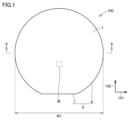
- FIG. 1 is a schematic plan view showing the configuration of a silicon carbide substrate according to this embodiment.
- FIG. 2 is a schematic cross-sectional view taken along line II-II in FIG.
- FIG. 3 is an enlarged plan view of region III in FIG.
- FIG. 4 is a schematic cross-sectional view taken along line IV-IV in FIG. 3.
- FIG. 5A is an enlarged schematic cross-sectional view of area VA in FIG. 4.
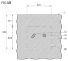
- FIG. FIG. 5B is an enlarged schematic cross-sectional view of region VB in FIG. 4.
- FIG. 6 is a perspective plan view showing the configuration of the first rectangular parallelepiped region.
- FIG. 7 is a perspective plan view showing the configuration of the second rectangular parallelepiped region.
- FIG. 8 is an enlarged schematic plan view of the second principal surface.
- FIG. 1 is a schematic plan view showing the configuration of a silicon carbide substrate according to this embodiment.
- FIG. 2 is a schematic cross-sectional view taken along line II-II in FIG.
- FIG. 9 is an enlarged schematic cross-sectional view of region IX in FIG.
- FIG. 10 is a schematic plan view showing a state in which the first principal surface is divided into a plurality of square regions.
- FIG. 11A is a schematic partial cross-sectional view showing the configuration of a silicon carbide crystal manufacturing apparatus according to this embodiment.
- FIG. 11B is a schematic diagram showing the relationship between temperature and time in the step of firing a crucible and a graphite member placed in the crucible.
- FIG. 12 is a schematic cross-sectional view showing a step of arranging a silicon carbide raw material and a seed substrate inside a crucible.
- FIG. 13 is a schematic cross-sectional view showing a silicon carbide crystal growth process.
- FIG. 11A is a schematic partial cross-sectional view showing the configuration of a silicon carbide crystal manufacturing apparatus according to this embodiment.
- FIG. 11B is a schematic diagram showing the relationship between temperature and time in the step of firing a crucible and
- FIG. 14 is an enlarged schematic diagram showing the configuration of region XIV in FIG. 13.
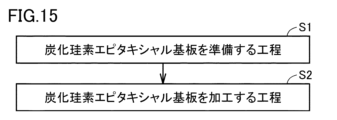
- FIG. 15 is a flowchart schematically showing a method for manufacturing a silicon carbide semiconductor device according to this embodiment.
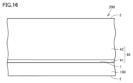
- FIG. 16 is a schematic cross-sectional view showing the structure of a silicon carbide epitaxial substrate according to this embodiment.
- FIG. 17 is a schematic cross-sectional view showing the process of forming the body region.
- FIG. 18 is a schematic cross-sectional view showing the process of forming a source region.
- FIG. 19 is a schematic cross-sectional view showing a step of forming a trench on the third main surface of the silicon carbide epitaxial layer.
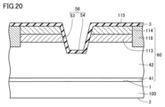
- FIG. 20 is a schematic cross-sectional view showing the process of forming a gate insulating film.
- FIG. 21 is a schematic cross-sectional view showing the process of forming a gate electrode and an interlayer insulating film.
- FIG. 22 is a schematic cross-sectional view showing the configuration of a silicon
- An object of the present disclosure is to provide a silicon carbide substrate, a silicon carbide epitaxial substrate, and a method for manufacturing a silicon carbide semiconductor device that can improve the yield of silicon carbide semiconductor devices.
- a silicon carbide substrate, a silicon carbide epitaxial substrate, and a method for manufacturing a silicon carbide semiconductor device that can improve the yield of silicon carbide semiconductor devices According to the present disclosure, it is possible to provide a silicon carbide substrate, a silicon carbide epitaxial substrate, and a method for manufacturing a silicon carbide semiconductor device that can improve the yield of silicon carbide semiconductor devices.
- Silicon carbide substrate 100 includes first main surface 1 and second main surface 2 on the opposite side of first main surface 1.
- a first void 10 exists in the first principal surface 1 .
- the areal density of the first voids 10 is less than 0.9 voids/cm 2 .
- the width of the first void 10 when viewed in the direction perpendicular to the first main surface 1 is 10 ⁇ m or more and 100 ⁇ m or less. When viewed in a direction parallel to the first main surface 1, the width of the first void 10 increases from the first main surface 1 toward the second main surface 2.
- the depth of first void 10 is smaller than the thickness of silicon carbide substrate 100 when viewed in a direction parallel to first main surface 1 .
- the first principal surface 1 is a carbon surface or a surface inclined at an off angle ⁇ of 8° or less with respect to the carbon surface.
- Silicon carbide substrate 100 includes first main surface 1 and second main surface 2 on the opposite side of first main surface 1.
- a first void 10 exists on the first main surface 1
- a second void 20 exists on the second main surface 2.
- the surface density of the second voids 20 is less than 0.9 voids/cm 2 .
- each of the first void 10 and the second void 20 has a width of 10 ⁇ m or more and 100 ⁇ m or less.
- the width of each of the first void 10 and the second void 20 increases from the first main surface 1 toward the second main surface 2.
- first void 10 and second void 20 are smaller than the thickness of silicon carbide substrate 100 when viewed in a direction parallel to first main surface 1 .
- the second principal surface 2 is a silicon surface or a surface inclined at an off angle ⁇ of 8° or less with respect to the silicon surface.
- the plurality of square regions 30 have a penetrating A first region 31 in which the areal density of screw dislocations 4 is 3000 pieces/cm 2 or more, a second region 32 in which the areal density of threading screw dislocations 4 is 1000 pieces/cm 2 or more and less than 3000 pieces/cm 2 , and
- the third region 33 may have a surface density of screw dislocations 4 of less than 1000 pieces/cm 2 .
- the ratio of the area of the first region 31 to the total area of the first region 31, the second region 32, and the third region 33 may be 1% or more and 10% or less.
- the ratio of the area of the first region 31 to the total area of the first region 31, the second region 32, and the third region 33 is 5% or more. There may be.
- the areal density of threading screw dislocations 4 on second main surface 2 may be 1500 pieces/cm 2 or less. .
- first carbon inclusions 71 are present in first rectangular parallelepiped region 61 of silicon carbide substrate 100. You may. In the direction perpendicular to the first main surface 1, the distance from the first main surface 1 to the upper end surface of the first rectangular parallelepiped region 61 is 50 ⁇ m, and the distance below the first main surface 1 and the first rectangular parallelepiped region 61 is 50 ⁇ m. The distance to the end face may be 200 ⁇ m.
- the length of the long side of the first rectangular parallelepiped region 61 is 0.82 mm, and the length of the short side of the first rectangular parallelepiped region 61 is 0.7 mm. It may be.
- the first void 10 may overlap the first rectangular parallelepiped region 61 when viewed in a direction perpendicular to the first main surface 1 .
- the maximum length of the first carbon inclusion 71 when viewed in the direction perpendicular to the first main surface 1 may be 5 ⁇ m or more and 50 ⁇ m or less.
- second carbon inclusions 72 are present in second rectangular parallelepiped region 62 of silicon carbide substrate 100. You may. In the direction perpendicular to the first main surface 1, the distance from the first main surface 1 to the upper end surface of the second rectangular parallelepiped region 62 is 50 ⁇ m, and the distance below the first main surface 1 and the second rectangular parallelepiped region 62 is 50 ⁇ m. The distance to the end face may be 200 ⁇ m.
- the length of the long side of the second rectangular parallelepiped region 62 is 0.82 mm, and the length of the short side of the second rectangular parallelepiped region 62 is 0.7 mm. It may be.
- the areal density of threading screw dislocations 4 in the region of the first main surface 1 overlapping with the second rectangular parallelepiped region 62 when viewed in the direction perpendicular to the first main surface 1 may be 3000 pieces/cm 2 or more.
- the maximum length of the second carbon inclusion 72 when viewed in the direction perpendicular to the first main surface 1 may be 5 ⁇ m or more and 50 ⁇ m or less.
- first main surface 1 may have a diameter of 150 mm or more.
- the first main surface 1 is a surface inclined at an off angle ⁇ of 1° or more and 4° or less with respect to the carbon surface. It may be.
- Silicon carbide epitaxial substrate 200 includes silicon carbide substrate 100 according to any one of (1) to (9) above, and silicon carbide epitaxial layer 60 provided on silicon carbide substrate 100. We are prepared.
- a method for manufacturing silicon carbide semiconductor device 400 according to the present disclosure includes the following steps. Silicon carbide epitaxial substrate 200 described in (10) above is prepared. Silicon carbide epitaxial substrate 200 is processed. [Details of embodiments of the present disclosure] Hereinafter, details of embodiments of the present disclosure will be described based on the drawings. In the following drawings, the same or corresponding parts are given the same reference numerals, and the description thereof will not be repeated. In the crystallographic descriptions in this specification, individual orientations are indicated by [], collective orientations are indicated by ⁇ >, individual planes are indicated by (), and collective planes are indicated by ⁇ , respectively. Regarding negative indexes, a "-" (bar) is supposed to be placed above the number in terms of crystallography, but in this specification, a negative sign is placed in front of the number.
- FIG. 1 is a schematic plan view showing the configuration of silicon carbide substrate 100 according to this embodiment.
- silicon carbide substrate 100 has first main surface 1 and outer peripheral side surface 9.
- the first main surface 1 extends along each of a first direction 101 and a second direction 102.
- the first direction 101 is, for example, the ⁇ 11-20> direction, although it is not particularly limited.
- the second direction 102 is, for example, the ⁇ 1-100> direction, although it is not particularly limited.
- the off direction is, for example, the first direction 101.
- Silicon carbide substrate 100 is made of, for example, hexagonal silicon carbide.
- the polytype of hexagonal silicon carbide is, for example, 4H.
- Silicon carbide substrate 100 contains, for example, n-type impurities such as nitrogen.
- the first main surface 1 is a carbon surface or a surface inclined in the off direction with respect to the carbon surface.
- the first principal surface 1 is a (000-1) plane or a plane inclined in the off direction with respect to the (000-1) plane.
- the second main surface 2 (see FIG. 2) is a silicon surface or a surface inclined in the off direction with respect to the silicon surface.
- the second principal surface 2 is a (0001) plane or a plane inclined in the off direction with respect to the (0001) plane.
- the outer peripheral side surface 9 has an orientation flat portion 7 and an arcuate portion 8.
- the arcuate portion 8 is continuous with the orientation flat portion 7.
- the orientation flat portion 7 extends along a first direction 101 when viewed from a direction perpendicular to the first main surface 1.
- the diameter W1 of the first main surface 1 is, for example, 150 mm.
- the diameter W1 may be 150 mm or more, or 200 mm or more.
- the upper limit of the diameter W1 is not particularly limited, but may be, for example, 300 mm or less. When viewed in a direction perpendicular to the first main surface 1, the diameter W1 is the longest straight distance between two different points on the outer circumferential side surface 9.
- FIG. 2 is a schematic cross-sectional view taken along line II-II in FIG. 1.
- the cross section shown in FIG. 2 is perpendicular to the first main surface 1 and parallel to the first direction 101.
- silicon carbide substrate 100 according to this embodiment has second main surface 2. As shown in FIG. The second main surface 2 is on the opposite side of the first main surface 1.
- Thickness E1 of silicon carbide substrate 100 is, for example, 300 ⁇ m or more and 700 ⁇ m or less.
- the third direction 103 is a direction perpendicular to each of the first direction 101 and the second direction 102.
- the thickness direction of silicon carbide substrate 100 is the same as third direction 103.
- the off angle ⁇ of the surface inclined in the off direction with respect to the carbon surface may be 8 degrees or less.
- the upper limit of the off-angle ⁇ is not particularly limited, but may be, for example, 6° or less, or 4° or less.
- the lower limit of the off-angle ⁇ is not particularly limited, but may be, for example, 1° or more, or 2° or more.
- the off direction of the surface inclined in the off direction with respect to the carbon surface is not particularly limited, but is, for example, the ⁇ 11-20> direction.
- FIG. 3 is an enlarged plan view of region III in FIG. 1.
- one or more first voids 10 are present in the first main surface 1.
- the opening of the first void 10 has a hexagonal shape, for example, when viewed in a direction perpendicular to the first main surface 1.
- the shape of the opening of the first void 10 is not particularly limited, and may be, for example, circular, oval, or polygonal other than hexagonal.
- the width of the first void 10 (first width A1) when viewed in the direction perpendicular to the first main surface 1 is 10 ⁇ m or more and 100 ⁇ m or less.
- the width of the first void 10 is the maximum width between any two points in the opening of the first void 10.
- the width of the first void 10 may be, for example, the width along the off direction.
- the lower limit of the first width A1 is not particularly limited, but may be, for example, 20 ⁇ m or more, or 30 ⁇ m or more.
- the upper limit of the first width A1 is not particularly limited, but may be, for example, 80 ⁇ m or less, or 60 ⁇ m or less.
- the surface density of the first voids 10 is less than 0.9 voids/cm 2 .
- the upper limit of the areal density of the first voids 10 is not particularly limited, but may be, for example, 0.6 voids/cm 2 or less, or 0.4 voids/cm 2 or less.
- the lower limit of the areal density of the first voids 10 is not particularly limited, but may be, for example, 0.02 voids/cm 2 or more, 0.05 voids/cm 2 or more, or 0.15 voids/cm 2 or more.
- the number of particles/cm 2 or more may be sufficient.
- FIG. 4 is a schematic cross-sectional view taken along line IV-IV in FIG. 3.
- the cross section shown in FIG. 4 is perpendicular to the first main surface 1 and parallel to the first direction 101.
- the width of the first void 10 increases from the first main surface 1 toward the second main surface 2 when viewed in a direction parallel to the first main surface 1.
- FIG. 5A is an enlarged schematic cross-sectional view of area VA in FIG. 4.
- the first void 10 has a first opening 11, a first side surface 12, and a first bottom 13.
- the first opening 11 is located on the first main surface 1.
- the first bottom portion 13 is located between the first main surface 1 and the second main surface 2.
- the first side surface portion 12 is located between the first opening portion 11 and the first bottom portion 13.
- the first side surface portion 12 is continuous with each of the first opening portion 11 and the first bottom portion 13 .
- the first side surface portion 12 may be linear.
- the shape of the first void 10 is, for example, a trapezoid when viewed in a direction parallel to the first main surface 1.
- the upper base of the trapezoid is located at the first opening 11 .
- the lower base of the trapezoid is located at the first base 13.
- the width of the first bottom portion 13 is larger than the width of the first opening 11 when viewed in a direction parallel to the first main surface 1 .
- first depth B1 The depth of first void 10 (first depth B1) is smaller than the thickness of silicon carbide substrate 100 when viewed in a direction parallel to first main surface 1 . In other words, first void 10 does not penetrate silicon carbide substrate 100 . The first void 10 is exposed only on the first main surface 1 and not on the second main surface 2.
- the first depth B1 may be greater than or equal to the width (first width A1) of the first void 10 on the first main surface 1.
- the first depth B1 may be the same as the first width A1 or may be larger than the first width A1.
- the upper limit of the first depth B1 is not particularly limited, but may be, for example, five times or less, or three times or less the width of the first bottom portion 13 of the first void 10.
- a carbon inclusion (first carbon inclusion 71) exists below the first void 10.
- the first carbon inclusion 71 may face the first bottom 13 of the first void 10 .
- First carbon inclusion 71 is embedded in silicon carbide region 15 of silicon carbide substrate 100 .
- the distance between first main surface 1 and first carbon inclusion 71 is, for example, 50 ⁇ m or more and 200 ⁇ m or less.
- the first carbon inclusion 71 exists in the first rectangular parallelepiped region 61 that is 50 ⁇ m or more and 200 ⁇ m or less away from the first main surface 1 toward the second main surface 2.
- first distance D11 the distance from the first main surface 1 to the upper end surface of the first rectangular parallelepiped region 61
- second distance D12 the distance from the first main surface 1 to the lower end surface of the first rectangular parallelepiped region 61
- third distance D13 the distance from the lower end surface to the upper end surface of the first rectangular parallelepiped region 61
- FIG. 5B is an enlarged schematic cross-sectional view of region VB in FIG. 4.
- first distance D21 the distance from the first main surface 1 to the upper end surface of the second rectangular parallelepiped region 62
- second distance D22 the distance from the first main surface 1 to the lower end surface of the second rectangular parallelepiped region 62
- third distance D23 the distance from the lower end surface to the upper end surface of the second rectangular parallelepiped region 62 (third distance D23) is 150 ⁇ m.
- FIG. 6 is a perspective plan view showing the configuration of the first rectangular parallelepiped region 61.
- the first rectangular parallelepiped region 61 has a rectangular shape when viewed in a direction perpendicular to the first principal surface 1.
- the length of the long side of the first rectangular parallelepiped region 61 (first length L11) is 0.82 mm.
- the long sides of the first rectangular parallelepiped region 61 are parallel to the first direction 101.
- the length of the short side (second length L12) of the first rectangular parallelepiped region 61 is 0.7 mm.
- the short sides of the first rectangular parallelepiped region 61 are parallel to the second direction 102 .
- the first void 10 overlaps with the first rectangular parallelepiped region 61 when viewed in a direction perpendicular to the first main surface 1 .
- the first rectangular parallelepiped region 61 is determined such that the center of the first void 10 coincides with the center of the first rectangular parallelepiped region 61 when viewed in a direction perpendicular to the first principal surface 1 .
- the maximum length F1 of the first carbon inclusion 71 when viewed in the direction perpendicular to the first main surface 1 is 5 ⁇ m or more and 50 ⁇ m or less.
- the first carbon inclusion 71 existing in the first rectangular parallelepiped region 61 is shown. As shown in FIG. 6, in the first rectangular parallelepiped region 61, there may be 10 or more and 20 or less first carbon inclusions 71.
- the lower limit of the number of first carbon inclusions 71 present in the first rectangular parallelepiped region 61 is not particularly limited, but may be, for example, 11 or more, or 12 or more.
- the upper limit of the number of first carbon inclusions 71 present in the first rectangular parallelepiped region 61 is not particularly limited, but may be, for example, 19 or less, or 18 or less.
- FIG. 7 is a perspective plan view showing the configuration of the second rectangular parallelepiped region 62.
- the shape of the second rectangular parallelepiped region 62 is rectangular when viewed in a direction perpendicular to the first principal surface 1.
- the length of the long side of the second rectangular parallelepiped region 62 (first length L21) is 0.82 mm.
- the long sides of the second rectangular parallelepiped region 62 are parallel to the first direction 101.
- the length of the short side (second length L22) of the second rectangular parallelepiped region 62 is 0.7 mm.
- the short sides of the second rectangular parallelepiped region 62 are parallel to the second direction 102.
- the second rectangular parallelepiped region 62 is a region spaced from the first main surface 1 toward the second main surface 2 by 50 ⁇ m or more and 200 ⁇ m or less. Above the second rectangular parallelepiped region 62, there is a region where threading screw dislocations 4 are concentrated. Specifically, when viewed in the direction perpendicular to the first principal surface 1, the areal density of threading screw dislocations 4 in the region of the first principal surface 1 overlapping with the second rectangular parallelepiped region 62 is 3000 dislocations/cm 2 or more. It is.
- the second rectangular parallelepiped is arranged so that the center of the region of the first main surface 1 that overlaps with the second rectangular parallelepiped region 62 coincides with the center of the first region 31, which will be described later, when viewed in a direction perpendicular to the first main surface 1. Region 62 is determined.
- the second rectangular parallelepiped region 62 includes a second carbon inclusion 72 .
- Second carbon inclusion 72 is embedded in silicon carbide region 15 of silicon carbide substrate 100 .
- the maximum length F2 of the second carbon inclusion 72 when viewed in the direction perpendicular to the first main surface 1 is 5 ⁇ m or more and 50 ⁇ m or less.
- a second carbon inclusion 72 existing in the second rectangular parallelepiped region 62 is shown. As shown in FIG. 7, in the second rectangular parallelepiped region 62, there are 3 or more and less than 10 second carbon inclusions 72.
- the lower limit of the number of second carbon inclusions 72 present in the second rectangular parallelepiped region 62 is not particularly limited, but may be, for example, four or more, or five or more.
- the upper limit of the number of second carbon inclusions 72 present in the second rectangular parallelepiped region 62 is not particularly limited, but may be less than nine or less than eight, for example.
- FIG. 8 is an enlarged schematic plan view of the second main surface 2. As shown in FIG. 8, one or more second voids 20 are present in the second main surface 2.
- the shape of the opening of the second void 20 when viewed in the direction perpendicular to the second main surface 2 is, for example, hexagonal.
- the shape of the opening of the second void 20 is not particularly limited, and may be, for example, circular, oval, or polygonal other than hexagonal.
- the width of the second void 20 (second width A2) when viewed in the direction perpendicular to the second main surface 2 is 10 ⁇ m or more and 100 ⁇ m or less.
- the width of the second void 20 is the maximum width between any two points in the opening of the second void 20.
- the width of the second void 20 may be, for example, the width along the off direction.
- the lower limit of the second width A2 is not particularly limited, but may be, for example, 20 ⁇ m or more, or 30 ⁇ m or more.
- the upper limit of the second width A2 is not particularly limited, but may be, for example, 80 ⁇ m or less, or 60 ⁇ m or less.
- the surface density of the second voids 20 is less than 0.9 voids/cm 2 .
- the upper limit of the areal density of the second voids 20 is not particularly limited, but may be, for example, 0.6 voids/cm 2 or less, or 0.4 voids/cm 2 or less.
- the lower limit of the areal density of the second voids 20 is not particularly limited, but may be, for example, 0.02 voids/cm 2 or more, 0.05 voids/cm 2 or more, or 0.15 voids/cm 2 or more.
- the number of particles/cm 2 or more may be sufficient.
- FIG. 9 is an enlarged schematic cross-sectional view of region IX in FIG. 4.
- the second void 20 has a second opening 21 , a second side surface 22 , and a second bottom 23 .
- the second opening 21 is located on the second main surface 2.
- the second bottom portion 23 is located between the first main surface 1 and the second main surface 2.
- the second side surface portion 22 is located between the second opening portion 21 and the second bottom portion 23.
- the second side surface portion 22 is continuous with each of the second opening portion 21 and the second bottom portion 23 .
- the second side surface portion 22 may be linear when viewed in a direction parallel to the second main surface 2.
- the shape of the second void 20 is, for example, a triangle when viewed in a direction parallel to the first main surface 1.
- the base of the triangle is located at the second opening 21.
- the apex of the triangle is located at the second bottom 23.
- the depth of second void 20 (second depth B2) is smaller than the thickness of silicon carbide substrate 100 when viewed in a direction parallel to first main surface 1 . In other words, second void 20 does not penetrate silicon carbide substrate 100 . The second void 20 is exposed only on the second main surface 2 and not on the first main surface 1.
- the second depth B2 may be greater than or equal to the width (second width A2) of the second void 20 on the second main surface 2.
- the second depth B2 may be the same as the second width A2, or may be larger than the second width A2.
- the upper limit of the second depth B2 is not particularly limited, but may be, for example, five times or less, or three times or less the width of the second opening 21 of the second void 20.
- third voids 14 are formed in silicon carbide substrate 100.
- Third void 14 is located inside silicon carbide substrate 100.
- Third void 14 is closed inside silicon carbide substrate 100 .
- the third void 14 is not exposed on either the first main surface 1 or the second main surface 2.
- the width of the third void 14 increases from the first main surface 1 toward the second main surface 2 .
- the shape of the third void 14 when viewed in a direction parallel to the first main surface 1 is, for example, a triangle.
- Each of the first void 10 and the second void 20 is identified using an optical microscope. It opens on the first main surface 1 and has a width of 10 ⁇ m or more and 100 ⁇ m or less when viewed in a direction perpendicular to the first main surface 1, and the width increases from the first main surface 1 toward the second main surface 2.
- a bottomed hole in which the value becomes larger is specified as the first void 10.
- the value obtained by dividing the number of first voids 10 in the measurement area of the first main surface 1 by the area of the measurement area of the first main surface 1 is taken as the areal density of the first voids 10. Note that the area within 5 mm from the outer circumferential side surface 9 on the first principal surface 1 is outside the measurement area.
- the second main surface 2 has a width of 10 ⁇ m or more and 100 ⁇ m or less when viewed in a direction perpendicular to the second main surface 2, and has an opening on the second main surface 2.
- a bottomed hole whose width increases toward the end is identified as the second void 20.
- the value obtained by dividing the number of second voids 20 in the measurement region of the second main surface 2 by the area of the measurement region of the second main surface 2 is taken as the areal density of the second voids 20. Note that the area within 5 mm from the outer circumferential side surface 9 on the second main surface 2 is outside the measurement area.
- FIG. 10 is a schematic plan view showing a state in which the measurement area of the first main surface 1 excluding the area within 5 mm from the outer peripheral side surface 9 is divided into a plurality of square areas 30.
- the length of one side of each of the plurality of square regions 30 is 5 mm.
- the first side of each of the plurality of square regions 30 is parallel to the first direction 101.
- the second side of each of the plurality of square regions 30 is parallel to the second direction 102.
- the second side is continuous with the first side.
- the number of square regions 30 increases from below to above the first main surface 1 along the second direction 102, for example, 7, 13, 17, 19, 21 pieces, 23 pieces, 23 pieces, 25 pieces, 25 pieces, 26 pieces, 27 pieces, 27 pieces, 27 pieces, 27 pieces, 27 pieces, 27 pieces, 27 pieces, 26 pieces, 25 pieces, 25 pieces, 23 pieces , 23, 21, 19, 17, 13, and 7.
- the plurality of square areas 30 include a first area 31, a second area 32, and a third area 33.
- the first region 31 is a region in which the surface density of threading screw dislocations 4 is 3000 pieces/cm 2 or more.
- the second region 32 is a region in which the areal density of threading screw dislocations 4 is 1000 or more/cm 2 or more and less than 3000/cm 2 .
- the third region 33 is a region in which the areal density of threading screw dislocations 4 is less than 1000 pieces/cm 2 .
- the ratio of the area of the first region 31 to the total area of the first region 31, the second region 32, and the third region 33 may be, for example, 1% or more and 10% or less.
- the lower limit of the ratio of the area of the first region 31 to the total area of the first region 31, the second region 32, and the third region 33 is not particularly limited, but may be, for example, 3% or more, or 5% or more. It may be.
- the upper limit of the ratio of the area of the first region 31 to the total area of the first region 31, the second region 32, and the third region 33 is not particularly limited, but may be, for example, 9% or less, or 8% or less. It may be.
- the surface density of threading screw dislocations 4 on the second main surface 2 is, for example, 1500 dislocations/cm 2 or less.
- the upper limit of the areal density of threading screw dislocations 4 on the second main surface 2 is not particularly limited, but may be, for example, 1400 dislocations/cm 2 or less, or 1300 dislocations/cm 2 or less.
- the lower limit of the areal density of threading screw dislocations 4 on the second main surface 2 is not particularly limited, but may be, for example, 500 dislocations/cm 2 or more, or 900 dislocations/cm 2 or more.
- the areal density of threading screw dislocations 4 is measured using, for example, molten potassium hydroxide (KOH). Specifically, etch pits are formed on the second main surface 2 by etching the silicon carbide region near the threading screw dislocations 4 exposed on the second main surface 2 by molten KOH. The observation area of the etch pit is, for example, 0.82 mm x 0.70 mm. The observation areas are set at equal intervals in each of the first direction 101 and the second direction 102. The pitch of the observation areas is 5 mm. In the molten KOH, at least one of sodium peroxide (Na 2 O 2 ), barium peroxide (BaO 2 ), and sodium nitrate (NaNO 3 ) may be added.
- KOH molten potassium hydroxide
- the number of etch pits caused by threading screw dislocations 4 is measured in all observation areas.
- the value obtained by dividing the total number of the etch pits in all observation areas by the total area of the observation areas corresponds to the areal density of threading screw dislocations 4 on the second main surface 2.
- the temperature of the KOH melt is, for example, approximately 500°C or higher and 550°C or lower.
- Etching time is about 5 minutes or more and 10 minutes or less.
- the observation area of the second principal surface 2 is observed using a Normalski differential interference microscope.
- FIG. 11A is a schematic partial cross-sectional view showing the configuration of a silicon carbide crystal manufacturing apparatus according to this embodiment.
- silicon carbide crystal manufacturing apparatus 300 mainly includes crucible 130, first resistance heater 141, second resistance heater 142, and third resistance heater 143.
- Crucible 130 is made of graphite.
- the crucible 130 has a raw material storage section 132 and a lid section 131.
- the lid part 131 is arranged on the raw material storage part 132.
- a graphite member (not shown) is placed inside the crucible 130.
- the first resistance heater 141 is arranged above the lid part 131.
- the second resistance heater 142 is arranged so as to surround the outer periphery of the raw material storage section 132.
- the third resistance heater 143 is arranged below the bottom surface of the raw material storage section 132.
- the crucible 130 is heated by applying electric power to the first resistance heater 141, the second resistance heater 142, and the third resistance heater 143.
- a method for manufacturing silicon carbide substrate 100 will be described.
- a step of firing a crucible and a graphite member placed in the crucible is performed. Specifically, a crucible and a graphite member disposed within the crucible are heated to a temperature of 3000° C. in an argon gas atmosphere.
- the heating time of the crucible is, for example, 10 hours.
- the pressure of argon gas is, for example, 10 kPa.
- FIG. 11B is a schematic diagram showing the relationship between temperature and time in the process of firing a crucible and a graphite member placed in the crucible.
- the vertical axis represents temperature and the horizontal axis represents time.
- the temperature of the crucible 130 increases from the first temperature C1 to the second temperature C2 from the first time T1 to the second time T2.
- the first temperature C1 is, for example, 1100°C.
- the second temperature C2 is, for example, 2200°C.
- the temperature of the crucible 130 increases from the second temperature C2 to the third temperature C3 from the second time T2 to the third time T3.
- the third temperature C3 is the highest temperature reached.
- the third temperature C3 is, for example, 3000°C.
- the temperature increase rate in the first temperature increase step is, for example, 100° C./hour.
- the temperature increase rate in the second temperature increase step is 20° C./hour or less.
- the temperature increase rate in the second temperature increase step is lower than the temperature increase rate in the first temperature increase step.
- a firing process is performed. From the third time T3 to the fourth time T4, the temperature of the crucible 130 is maintained at the third temperature C3. The time from the third time point T3 to the fourth time point T4 is the firing time.
- a cooling step is performed. The crucible 130 is cooled from the fourth time point T4. In order to prevent the member from cracking, the crucible 130 is slowly cooled until the temperature of the crucible 130 reaches the first temperature C1. The cooling rate of the crucible 130 is 20° C./hour or less.
- the pressure of the atmospheric gas in the crucible 130 is maintained at, for example, about 10 kPa.
- the atmospheric gas contains an inert gas such as argon gas or helium gas.
- FIG. 12 is a schematic cross-sectional view showing a step of arranging a silicon carbide raw material and a seed substrate inside a crucible.
- silicon carbide raw material 153 is placed in raw material storage section 132.
- Silicon carbide raw material 153 is, for example, polycrystalline silicon carbide powder.
- Seed substrate 150 is fixed to lid 131 using, for example, an adhesive (not shown).
- Seed substrate 150 has a growth surface 151 and a mounting surface 152. Attachment surface 152 is on the opposite side from growth surface 151.
- Growth surface 151 faces silicon carbide raw material 153.
- the mounting surface 152 faces the lid portion 131.
- Growth surface 151 of seed substrate 150 is arranged to face the surface of silicon carbide raw material 153.
- Seed substrate 150 is, for example, a silicon carbide single crystal substrate whose polytype is 4H.
- the diameter of the growth surface 151 is, for example, 150 mm.
- the diameter of the growth surface 151 may be 150 mm or more.
- the growth surface 151 is, for example, a carbon surface or a surface inclined at an off angle of about 8° or less with respect to the carbon surface. As described above, seed substrate 150 and silicon carbide raw material 153 are prepared.
- FIG. 13 is a schematic cross-sectional view showing the growth process of silicon carbide crystal.
- the pressure in crucible 130 is reduced while the temperature of growth surface 151 of seed substrate 150 is lower than the temperature of silicon carbide raw material 153.
- the pressure of the atmospheric gas in the crucible 130 is reduced to, for example, 1.0 kPa.
- silicon carbide raw material 153 starts to sublimate, and the sublimated silicon carbide gas recrystallizes on growth surface 151 of seed substrate 150 .
- Single crystal growth of silicon carbide crystal 110 begins on growth surface 151 of seed substrate 150 .
- the pressure within crucible 130 is maintained at, for example, approximately 0.1 kPa or more and 3 kPa or less.
- silicon carbide crystal 110 is grown on seed substrate 150 by subliming silicon carbide raw material 153.
- the temperature of silicon carbide crystal 110 is, for example, 2100° C. or higher and 2300° C. or lower.
- the lower limit of the temperature of silicon carbide crystal 110 is not particularly limited, but may be, for example, 2125° C. or higher, or 2150° C. or higher.
- the upper limit of the temperature of silicon carbide crystal 110 is not particularly limited, but may be, for example, 2250° C. or lower or 2275° C. or lower.
- FIG. 14 is an enlarged schematic diagram showing the configuration of region XIV in FIG. 13.
- a plurality of third voids 14 are formed inside silicon carbide crystal 110.
- each of the plurality of third voids 14 has a triangular shape, for example.
- the width of third void 14 in the direction perpendicular to the growth direction of silicon carbide crystal 110 becomes narrower along the growth direction of silicon carbide crystal 110. From another perspective, the width of third void 14 in the direction perpendicular to the growth direction of silicon carbide crystal 110 becomes narrower as it goes from seed substrate 150 toward silicon carbide raw material 153.
- silicon carbide crystal 110 is sliced. Specifically, silicon carbide crystal 110 is sliced along a plane perpendicular to the central axis of silicon carbide crystal 110 using, for example, a saw wire. Thereby, a plurality of silicon carbide substrates 100 are obtained (see FIG. 4). As shown in FIG. 4, silicon carbide substrate 100 has first main surface 1 and second main surface 2. As shown in FIG. Among the plurality of third voids 14 , the voids exposed on the first main surface 1 are the first voids 10 . Among the plurality of third voids 14 , the voids exposed on the second main surface 2 are second voids 20 .
- FIG. 15 is a flowchart schematically showing a method for manufacturing silicon carbide semiconductor device 400 according to this embodiment.
- the method for manufacturing silicon carbide semiconductor device 400 according to the present embodiment includes a step of preparing silicon carbide epitaxial substrate 200 (S1), and a step of processing silicon carbide epitaxial substrate 200 (S2). It mainly has
- a step (S1) of preparing silicon carbide epitaxial substrate 200 is performed.
- silicon carbide substrate 100 according to this embodiment is prepared (see FIG. 1).
- silicon carbide epitaxial layer 60 is formed on silicon carbide substrate 100.
- silicon carbide epitaxial layer 60 is formed on first main surface 1 of silicon carbide substrate 100 by epitaxial growth.
- silane (SiH 4 ) and propane (C 3 H 8 ) are used as source gases, and hydrogen (H 2 ) is used as a carrier gas.
- the temperature for epitaxial growth is, for example, about 1400° C. or more and 1700° C. or less.
- an n-type impurity, such as nitrogen, is introduced into silicon carbide epitaxial layer 60.
- FIG. 16 is a schematic cross-sectional view showing the configuration of silicon carbide epitaxial substrate 200 according to this embodiment.
- first void 10, second void 20, third void 14, first carbon inclusion 71, and second carbon inclusion 72 is omitted in the drawings after FIG. 16.
- silicon carbide epitaxial substrate 200 includes silicon carbide substrate 100 and silicon carbide epitaxial layer 60. Silicon carbide epitaxial layer 60 is provided on silicon carbide substrate 100. Silicon carbide epitaxial layer 60 has third main surface 3 . Third main surface 3 constitutes the surface of silicon carbide epitaxial substrate 200 . Second main surface 2 constitutes the back surface of silicon carbide epitaxial substrate 200 .
- Silicon carbide epitaxial layer 60 may include buffer layer 41 and drift layer 42 .
- Buffer layer 41 is in contact with silicon carbide substrate 100 at first main surface 1 .
- Drift layer 42 is provided on buffer layer 41.
- Each of the buffer layer 41 and the drift layer 42 contains an n-type impurity such as nitrogen.
- the concentration of n-type impurities contained in the buffer layer 41 may be higher than the concentration of n-type impurities contained in the drift layer 42.
- a step (S2) of processing silicon carbide epitaxial substrate 200 is performed. Specifically, the following processing is performed on silicon carbide epitaxial substrate 200. First, ion implantation is performed into silicon carbide epitaxial substrate 200.
- FIG. 17 is a schematic cross-sectional view showing the process of forming the body region.
- a p-type impurity such as aluminum is ion-implanted into third main surface 3 of silicon carbide epitaxial layer 60 .
- body region 113 having p-type conductivity is formed.
- the portion where body region 113 is not formed becomes drift layer 42 and buffer layer 41.
- the thickness of the body region 113 is, for example, 0.9 ⁇ m.
- Silicon carbide epitaxial layer 60 includes buffer layer 41 , drift layer 42 , and body region 113 .
- FIG. 18 is a schematic cross-sectional view showing the process of forming a source region.
- an n-type impurity such as phosphorus is ion-implanted into body region 113, for example.
- a source region 114 having an n-type conductivity type is formed.
- the thickness of the source region 114 is, for example, 0.4 ⁇ m.
- the concentration of n-type impurities contained in source region 114 is higher than the concentration of p-type impurities contained in body region 113.
- a contact region 118 is formed by ion-implanting a p-type impurity such as aluminum into the source region 114.
- Contact region 118 is formed to penetrate source region 114 and body region 113 and be in contact with drift layer 42 .
- the concentration of p-type impurities contained in contact region 118 is higher than the concentration of n-type impurities contained in source region 114.
- activation annealing is performed to activate the ion-implanted impurities.
- the activation annealing temperature is, for example, 1500° C. or more and 1900° C. or less.
- the activation annealing time is, for example, about 30 minutes.
- the activation annealing atmosphere is, for example, an argon atmosphere.
- FIG. 19 is a schematic cross-sectional view showing a step of forming a trench in third main surface 3 of silicon carbide epitaxial layer 60.
- a mask 117 having an opening is formed on the third main surface 3 composed of the source region 114 and the contact region 118. Using mask 117, source region 114, body region 113, and a portion of drift layer 42 are removed by etching.
- the etching method for example, inductively coupled plasma reactive ion etching can be used. Specifically, for example, inductively coupled plasma reactive ion etching using SF 6 or a mixed gas of SF 6 and O 2 as a reactive gas is used. A recess is formed in the third main surface 3 by etching.
- thermal etching is performed in the recesses.
- Thermal etching can be performed, for example, by heating in an atmosphere containing a reactive gas containing at least one type of halogen atom, with the mask 117 formed on the third main surface 3.
- At least one type of halogen atom includes at least one of a chlorine (Cl) atom and a fluorine (F) atom.
- the atmosphere includes, for example, Cl2 , BCl3 , SF6 or CF4 .
- thermal etching is performed using a mixed gas of chlorine gas and oxygen gas as a reaction gas, and at a heat treatment temperature of, for example, 700° C. or higher and 1000° C. or lower.
- the reaction gas may contain a carrier gas in addition to the above-mentioned chlorine gas and oxygen gas.
- the carrier gas for example, nitrogen gas, argon gas, or helium gas can be used.
- trenches 56 are formed in the third main surface 3 by thermal etching.
- Trench 56 is defined by side wall surface 53 and bottom wall surface 54 .
- Sidewall surface 53 is composed of source region 114, body region 113, and drift layer 42.
- the bottom wall surface 54 is composed of the drift layer 42.
- the mask 117 is removed from the third main surface 3.
- FIG. 20 is a schematic cross-sectional view showing the process of forming a gate insulating film.
- silicon carbide epitaxial substrate 200 in which trenches 56 are formed in third main surface 3 is heated at a temperature of, for example, 1300° C. or more and 1400° C. or less in an atmosphere containing oxygen.
- the bottom wall surface 54 is in contact with the drift layer 42
- the side wall surface 53 is in contact with each of the drift layer 42 , the body region 113 , and the source region 114
- the third main surface 3 is in contact with each of the source region 114 and the contact region 118 .
- a contacting gate insulating film 115 is formed.
- FIG. 21 is a schematic cross-sectional view showing the process of forming a gate electrode and an interlayer insulating film.
- Gate electrode 127 is formed inside trench 56 so as to be in contact with gate insulating film 115 .
- Gate electrode 127 is disposed inside trench 56 and formed on gate insulating film 115 so as to face each of side wall surface 53 and bottom wall surface 54 of trench 56 .
- the gate electrode 127 is formed, for example, by LPCVD (Low Pressure Chemical Vapor Deposition) method.
- Interlayer insulating film 126 is formed. Interlayer insulating film 126 is formed to cover gate electrode 127 and to be in contact with gate insulating film 115 .
- the interlayer insulating film 126 is formed, for example, by chemical vapor deposition.
- the interlayer insulating film 126 is made of, for example, a material containing silicon dioxide.
- interlayer insulating film 126 and a portion of gate insulating film 115 are etched so that openings are formed over source region 114 and contact region 118. As a result, contact region 118 and source region 114 are exposed from gate insulating film 115.
- Source electrode 116 is formed so as to be in contact with each of source region 114 and contact region 118.
- Source electrode 116 is formed by, for example, a sputtering method.
- the source electrode 116 is made of a material containing, for example, Ti (titanium), Al (aluminum), and Si (silicon).
- alloying annealing is performed. Specifically, the source electrode 116 in contact with each of the source region 114 and the contact region 118 is maintained at a temperature of, for example, 900° C. or more and 1100° C. or less for about 5 minutes. As a result, at least a portion of the source electrode 116 is silicided. As a result, a source electrode 116 that is in ohmic contact with the source region 114 is formed. Source electrode 116 may be in ohmic contact with contact region 118.
- Source wiring 119 is formed.
- Source wiring 119 is electrically connected to source electrode 116.
- Source wiring 119 is formed to cover source electrode 116 and interlayer insulating film 126 .
- a step of forming a drain electrode is performed. First, silicon carbide substrate 100 is polished on second main surface 2 . This reduces the thickness of silicon carbide substrate 100. Next, drain electrode 123 is formed. Drain electrode 123 is formed so as to be in contact with second main surface 2 . Through the above steps, silicon carbide semiconductor device 400 according to this embodiment is manufactured.
- FIG. 22 is a schematic cross-sectional view showing the configuration of silicon carbide semiconductor device 400 according to this embodiment.
- Silicon carbide semiconductor device 400 is, for example, a MOSFET (Metal Oxide Semiconductor Field Effect Transistor).
- Silicon carbide semiconductor device 400 mainly includes silicon carbide epitaxial substrate 200, gate electrode 127, gate insulating film 115, source electrode 116, drain electrode 123, source wiring 119, and interlayer insulating film 126. ing.
- Silicon carbide epitaxial substrate 200 has buffer layer 41 , drift layer 42 , body region 113 , source region 114 , and contact region 118 .
- Silicon carbide semiconductor device 400 may be, for example, an IGBT (Insulated Gate Bipolar Transistor).
- voids new defects existing in silicon carbide crystals. Unlike micropipes, voids do not penetrate through the silicon carbide crystal. Further, the width of the void is usually larger than the width of the micropipe. Furthermore, the width of the void is characterized by decreasing toward the growth direction.
- silicon carbide semiconductor device 400 is manufactured using silicon carbide substrate 100 having voids exposed on the main surface, the reliability of silicon carbide semiconductor device 400 may decrease. As a result, the yield of silicon carbide semiconductor device 400 may decrease.
- silicon carbide substrate 100 As a result of further intensive investigation into the causes of densely incorporated carbon inclusions of a certain size in silicon carbide substrate 100, we found that when growing silicon carbide crystals using a crucible made of graphite, It was found that carbon lumps generated from the placed graphite member were incorporated into the silicon carbide crystal. Therefore, the inventor discovered that by firing a graphite crucible and the graphite members placed in the crucible under specific conditions before the growth of silicon carbide crystals, carbon lumps were mixed into the silicon carbide crystals. We have found that it is possible to suppress this. Thereby, silicon carbide substrate 100 with reduced areal density of voids can be obtained.
- first void 10 exists in first main surface 1 .
- the areal density of the first voids 10 is less than 0.9 voids/cm 2 .
- the width of the first void 10 when viewed in the direction perpendicular to the first main surface 1 is 10 ⁇ m or more and 100 ⁇ m or less. When viewed in a direction parallel to the first main surface 1, the width of the first void 10 increases from the first main surface 1 toward the second main surface 2.
- the depth of first void 10 is smaller than the thickness of silicon carbide substrate 100 when viewed in a direction parallel to first main surface 1 .
- the first principal surface 1 is a carbon surface or a surface inclined at an off angle ⁇ of 8° or less with respect to the carbon surface.
- Silicon carbide substrate 100 includes first main surface 1 and second main surface 2 on the opposite side of first main surface 1 .
- a first void 10 exists on the first main surface 1
- a second void 20 exists on the second main surface 2.
- the surface density of the second voids 20 is less than 0.9 voids/cm 2 .
- each of the first void 10 and the second void 20 has a width of 10 ⁇ m or more and 100 ⁇ m or less.
- the width of each of the first void 10 and the second void 20 increases from the first main surface 1 toward the second main surface 2.
- first void 10 and second void 20 are smaller than the thickness of silicon carbide substrate 100 when viewed in a direction parallel to first main surface 1 .
- the second principal surface 2 is a silicon surface or a surface inclined at an off angle ⁇ of 8° or less with respect to the silicon surface.
- silicon carbide semiconductor device 400 When manufacturing silicon carbide semiconductor device 400 using silicon carbide substrate 100 described above, the yield of silicon carbide semiconductor device 400 can be improved.
- the plurality of square regions 30 when first main surface 1 is divided into a plurality of square regions 30 each side of which is 5 mm, the plurality of square regions 30 have an areal density of threading screw dislocations 4 of 3000.
- the first region 31 has an areal density of threading screw dislocations 4 of 1,000 or more but less than 3,000/cm 2
- the second region 32 has an areal density of threading screw dislocations 4 of 1,000 or more but less than 3,000/cm 2
- the third region 33 may have a smaller number of particles/cm 2 .
- the ratio of the area of the first region 31 to the total area of the first region 31, the second region 32, and the third region 33 may be 1% or more and 10% or less. Thereby, the yield of silicon carbide semiconductor device 400 can be further improved.
- the ratio of the area of first region 31 to the total area of first region 31, second region 32, and third region 33 may be 5% or more. . Thereby, the yield of silicon carbide semiconductor device 400 can be further improved.
- the areal density of threading screw dislocations 4 on second main surface 2 may be 1500 pieces/cm 2 or less. Thereby, the yield of silicon carbide semiconductor device 400 can be further improved.
- first carbon inclusions 71 are present in first rectangular parallelepiped region 61 that is 50 ⁇ m or more and 200 ⁇ m or less away from first main surface 1 toward second main surface 2. There may be 20 or less.
- the length of the long side of the first rectangular parallelepiped region 61 is 0.82 mm, and the length of the short side of the first rectangular parallelepiped region 61 is 0.7 mm. It may be.
- the first void 10 may overlap the first rectangular parallelepiped region 61 when viewed in a direction perpendicular to the first main surface 1 .
- the maximum length of the first carbon inclusion 71 when viewed in the direction perpendicular to the first main surface 1 may be 5 ⁇ m or more and 50 ⁇ m or less. Thereby, the yield of silicon carbide semiconductor device 400 can be further improved.
- second carbon inclusions 72 are present in second rectangular parallelepiped region 62 that is 50 ⁇ m or more and 200 ⁇ m or less away from first main surface 1 toward second main surface 2. Less than 10 may be present.
- the length of the long side of the second rectangular parallelepiped region 62 is 0.82 mm
- the length of the short side of the second rectangular parallelepiped region 62 is 0.7 mm. It may be.
- the areal density of threading screw dislocations 4 in the region of the first main surface 1 overlapping with the second rectangular parallelepiped region 62 when viewed in the direction perpendicular to the first main surface 1 may be 3000 pieces/cm 2 or more.
- the maximum length of the second carbon inclusion 72 when viewed in the direction perpendicular to the first main surface 1 may be 5 ⁇ m or more and 50 ⁇ m or less. Thereby, the yield of silicon carbide semiconductor device 400 can be further improved.
- the diameter of first main surface 1 may be 150 mm or more. Therefore, when silicon carbide substrate 100 with a large diameter is used, the yield of silicon carbide semiconductor device 400 can be further improved.
- Example 1 silicon carbide substrate 100 was manufactured using manufacturing conditions related to Samples 1 to 7. Under the manufacturing conditions for Samples 1 to 6, a firing process was performed. Specifically, the crucible 130 and the graphite member to be inside the crucible 130 were fired using the temperature profile shown in FIG. 11B. The third temperature C3 in FIG. 11B is the firing temperature. The time from the third time point T3 to the fourth time point T4 is the firing time. Under the manufacturing conditions for Sample 7, no firing step was performed.
- the firing temperature under the manufacturing conditions for Samples 1 and 2 was 2800°C.
- the firing temperature under the manufacturing conditions for Samples 3 to 6 was 3000°C.
- the firing time under the manufacturing conditions for Samples 1 and 4 was 10 hours.
- the firing time under the manufacturing conditions for Samples 2 and 5 was 30 hours.
- the firing time under the manufacturing conditions for Sample 6 was 60 hours.
- the firing time under the manufacturing conditions for Sample 3 was 0 minutes.
- silicon carbide crystal 110 was manufactured using crucible 130. As shown in FIG. 12, silicon carbide raw material 153 and seed substrate 150 were placed inside crucible 130. Silicon carbide crystal 110 was grown on seed substrate 150 using a sublimation method. After the growth of silicon carbide crystal 110 was completed, silicon carbide crystal 110 was sliced using a saw wire. Thereby, silicon carbide substrate 100 was cut out. Silicon carbide substrate 100 has first main surface 1 and second main surface 2. Silicon carbide substrate 100 has first main surface 1 and second main surface 2. The first main surface 1 was a surface inclined in the off direction with respect to the carbon surface. The off direction was set to ⁇ 11-20>. The off angle ⁇ was 2°. Through the above steps, silicon carbide substrates 100 for each of Samples 1 to 7 were prepared.
- the areal density of first voids 10 was measured. Specifically, the number of first voids 10 exposed on first main surface 1 of silicon carbide substrate 100 was measured. The first void 10 was identified using an optical microscope. A first void with a bottom, which has a width of 10 ⁇ m or more and 100 ⁇ m or less when viewed in a direction perpendicular to the first main surface 1, and whose width increases from the first main surface 1 to the second main surface 2. It was identified as 10. The value obtained by dividing the number of first voids 10 in the measurement area of the first main surface 1 by the area of the measurement area of the first main surface 1 was defined as the areal density of the first voids 10.
- the number of first carbon inclusions 71 under a certain first void 10 was counted. Specifically, in the region where the first void 10 is located on the first main surface 1, the focus of the microscope is shifted from the first main surface 1 to the second main surface 2 of the silicon carbide substrate 100 by the measurement depth. The number of first carbon inclusions 71 was visually counted. The measurement depth was 100 ⁇ m. The length of the long side of the measurement area was 0.21 mm. The length of the short side of the measurement area was 0.18 mm.
- Table 1 shows the areal density of first voids 10 in silicon carbide substrate 100 for each of Samples 1 to 7.
- the areal density of first voids 10 in silicon carbide substrate 100 for each of Samples 1 to 6 was lower than the areal density of first voids 10 in silicon carbide substrate 100 for Sample 7. .
- the longer the firing time the lower the areal density of the first voids 10.
- the higher the firing temperature the lower the areal density of the first voids 10.
- the numbers of first carbon inclusions 71 were 6, 3, 2, and 9, respectively.
- Example 2 (Measuring method) In silicon carbide substrate 100 for each of Samples 4 and 7, first region 31, second region 32, and third region 33 were identified.
- the first region 31 is a region in which the surface density of threading screw dislocations 4 is 3000 pieces/cm 2 or more.
- the second region 32 is a region in which the areal density of threading screw dislocations 4 is 1000 or more/cm 2 or more and less than 3000/cm 2 .
- the third region 33 is a region in which the areal density of threading screw dislocations 4 is less than 1000 pieces/cm 2 .
- the ratio of the area of the first region 31 to the total area of the first region 31, the second region 32, and the third region 33 was measured.
- the areal density of threading screw dislocations 4 was measured.
- the areal density of threading screw dislocations 4 was measured using molten potassium hydroxide (KOH).
- KOH molten potassium hydroxide
- the observation area of the etch pit is 0.82 mm x 0.70 mm.
- the pitch of the observation areas was 5 mm.
- the number of etch pits caused by threading screw dislocations 4 is measured.
- the value obtained by dividing the total number of the etch pits in all observation areas by the total area of the observation areas was taken as the areal density of threading screw dislocations 4 on the second main surface 2.
- the temperature of the KOH melt was approximately 500°C or higher and 550°C or lower.
- the etching time was about 5 minutes or more and 10 minutes or less.
- Table 2 shows the first region ratio, the second region ratio, the third region ratio, and the areal density of threading screw dislocations 4 on the second main surface 2.
- the first area ratio of silicon carbide substrate 100 according to Sample 4 was lower than the first area ratio of silicon carbide substrate 100 according to Sample 7. This confirmed that the first area ratio could be reduced by performing the firing process.
- the areal density of threading screw dislocations 4 on second main surface 2 of silicon carbide substrate 100 according to sample 4 was lower than the areal density of threading screw dislocations 4 on second main surface 2 of silicon carbide substrate 100 according to sample 7. . This confirmed that the areal density of threading screw dislocations 4 on the second main surface 2 could be reduced by performing the firing process.
- a silicon carbide substrate comprising a first main surface and a second main surface opposite to the first main surface, A first void is present in the first main surface, The areal density of the first void is less than 0.9 voids/cm 2 , When viewed in a direction perpendicular to the first main surface, the width of the first void is 10 ⁇ m or more and 100 ⁇ m or less, When viewed in a direction parallel to the first main surface, the width of the first void increases from the first main surface toward the second main surface, When viewed in a direction parallel to the first main surface, the depth of the first void is smaller than the thickness of the silicon carbide substrate,
- the first main surface is a silicon carbide substrate, wherein the first main surface is a carbon surface or a surface inclined at an off angle of 8 degrees or less with respect to the carbon surface.
- a silicon carbide substrate comprising a first main surface and a second main surface opposite to the first main surface, A first void exists on the first main surface, and a second void exists on the second main surface, The surface density of the second void is less than 0.9 voids/cm 2 , When viewed in a direction perpendicular to the first main surface, each of the first void and the second void has a width of 10 ⁇ m or more and 100 ⁇ m or less, When viewed in a direction parallel to the first main surface, the width of each of the first void and the second void increases from the first main surface toward the second main surface, When viewed in a direction parallel to the first main surface, the depth of each of the first void and the second void is smaller than the thickness of the silicon carbide substrate,
- the second main surface is a silicon carbide substrate, wherein the second main surface is a silicon surface or a surface inclined at an off angle of 8 degrees or less with respect to the silicon surface.
- the plurality of square regions are divided into a first region having an areal density of threading screw dislocations of 3000 pieces/cm 2 or more, and a first region having a surface density of threading screw dislocations of 3000 pieces/cm 2 or more;
- the second region has an areal density of 1000 pieces/cm 2 or more and less than 3000 pieces/cm 2
- a third region has an areal density of threading screw dislocations of less than 1000 pieces/cm 2
- the silicon carbide substrate according to appendix 1 or 2 wherein the ratio of the area of the first region to the total area of the first region, the second region, and the third region is 1% or more and 10% or less.
- the first void overlaps the first rectangular parallelepiped region,
- Appendix 7 3 or more and less than 10 second carbon inclusions are present in the second rectangular parallelepiped region of the silicon carbide substrate, In the direction perpendicular to the first main surface, the distance from the first main surface to the upper end surface of the second rectangular parallelepiped region is 50 ⁇ m, and the distance from the first main surface to the upper end surface of the second rectangular parallelepiped region is 50 ⁇ m.
- the distance to the end face is 200 ⁇ m
- the length of the long side of the second rectangular parallelepiped region is 0.82 mm
- the length of the short side of the second rectangular parallelepiped region is 0.7 mm.
- the areal density of threading screw dislocations in the region of the first main surface that overlaps with the second rectangular parallelepiped region is 3000 pieces/cm 2 or more
- the silicon carbide substrate according to Appendix 1 or 2 wherein the second carbon inclusion has a maximum length of 5 ⁇ m or more and 50 ⁇ m or less when viewed in a direction perpendicular to the first main surface.
- (Appendix 8) The silicon carbide substrate according to Supplementary Note 1 or 2, wherein the first principal surface has a diameter of 150 mm or more.
- (Appendix 9) The silicon carbide substrate according to Supplementary Note 1 or 2, wherein the first main surface is a surface inclined at an off angle of 1° or more and 4° or less with respect to the carbon surface.
- (Appendix 10) A silicon carbide substrate according to Supplementary Note 1 or 2, A silicon carbide epitaxial substrate, comprising: a silicon carbide epitaxial layer provided on the silicon carbide substrate. (Appendix 11) a step of preparing a silicon carbide epitaxial substrate according to Appendix 10; A method for manufacturing a silicon carbide semiconductor device, comprising the step of processing the silicon carbide epitaxial substrate.
- First principal surface 1. First principal surface, 2. Second principal surface, 3. Third principal surface, 4. Threading screw dislocation, 7. Orientation flat section, 8. Arc-shaped section, 9. Outer peripheral side surface, 10. First void, 11. First opening, 12. 1 side surface, 13 first bottom, 14 third void, 15 silicon carbide region, 20 second void, 21 second opening, 22 second side, 23 second bottom, 30 square region, 31 first region, 32 second region, 33 third region, 41 buffer layer, 42 drift layer, 53 side wall surface, 54 bottom wall surface, 56 trench, 60 silicon carbide epitaxial layer, 61 first rectangular parallelepiped region, 62 second rectangular parallelepiped region, 71 first Carbon inclusion, 72 Second carbon inclusion, 100 Silicon carbide substrate, 101 First direction, 102 Second direction, 103 Third direction, 110 Silicon carbide crystal, 113 Body region, 114 Source region, 115 Gate insulating film, 116 Source electrode , 117 mask, 118 contact region, 119 source wiring, 123 drain electrode, 126 interlayer insulating film, 127 gate electrode, 130
Landscapes
- Chemical & Material Sciences (AREA)
- Engineering & Computer Science (AREA)
- Crystallography & Structural Chemistry (AREA)
- Materials Engineering (AREA)
- Metallurgy (AREA)
- Organic Chemistry (AREA)
- Chemical Kinetics & Catalysis (AREA)
- General Chemical & Material Sciences (AREA)
- Inorganic Chemistry (AREA)
- Crystals, And After-Treatments Of Crystals (AREA)
Priority Applications (2)
| Application Number | Priority Date | Filing Date | Title |
|---|---|---|---|
| JP2024524250A JPWO2023233887A1 (https=) | 2022-06-02 | 2023-04-27 | |
| US18/860,672 US20250203985A1 (en) | 2022-06-02 | 2023-04-27 | Silicon carbide substrate, silicon carbide epitaxial substrate, and method of manufacturing silicon carbide semiconductor device |
Applications Claiming Priority (2)
| Application Number | Priority Date | Filing Date | Title |
|---|---|---|---|
| JP2022090216 | 2022-06-02 | ||
| JP2022-090216 | 2022-06-02 |
Publications (1)
| Publication Number | Publication Date |
|---|---|
| WO2023233887A1 true WO2023233887A1 (ja) | 2023-12-07 |
Family
ID=89026121
Family Applications (1)
| Application Number | Title | Priority Date | Filing Date |
|---|---|---|---|
| PCT/JP2023/016669 Ceased WO2023233887A1 (ja) | 2022-06-02 | 2023-04-27 | 炭化珪素基板、炭化珪素エピタキシャル基板および炭化珪素半導体装置の製造方法 |
Country Status (3)
| Country | Link |
|---|---|
| US (1) | US20250203985A1 (https=) |
| JP (1) | JPWO2023233887A1 (https=) |
| WO (1) | WO2023233887A1 (https=) |
Cited By (1)
| Publication number | Priority date | Publication date | Assignee | Title |
|---|---|---|---|---|
| WO2025121062A1 (ja) * | 2023-12-08 | 2025-06-12 | 住友電気工業株式会社 | 炭化珪素基板、エピタキシャル基板および半導体装置の製造方法 |
Citations (3)
| Publication number | Priority date | Publication date | Assignee | Title |
|---|---|---|---|---|
| JP2011190154A (ja) * | 2010-03-16 | 2011-09-29 | Sumitomo Electric Ind Ltd | 結晶の製造方法、結晶の製造装置および積層膜 |
| JP2019026500A (ja) * | 2017-07-28 | 2019-02-21 | 東洋炭素株式会社 | 単結晶SiCの製造方法、SiCインゴットの製造方法、SiCウエハの製造方法、及び単結晶SiC |
| WO2021215120A1 (ja) * | 2020-04-22 | 2021-10-28 | 住友電気工業株式会社 | 炭化珪素単結晶および炭化珪素単結晶の製造方法 |
-
2023
- 2023-04-27 WO PCT/JP2023/016669 patent/WO2023233887A1/ja not_active Ceased
- 2023-04-27 US US18/860,672 patent/US20250203985A1/en active Pending
- 2023-04-27 JP JP2024524250A patent/JPWO2023233887A1/ja active Pending
Patent Citations (3)
| Publication number | Priority date | Publication date | Assignee | Title |
|---|---|---|---|---|
| JP2011190154A (ja) * | 2010-03-16 | 2011-09-29 | Sumitomo Electric Ind Ltd | 結晶の製造方法、結晶の製造装置および積層膜 |
| JP2019026500A (ja) * | 2017-07-28 | 2019-02-21 | 東洋炭素株式会社 | 単結晶SiCの製造方法、SiCインゴットの製造方法、SiCウエハの製造方法、及び単結晶SiC |
| WO2021215120A1 (ja) * | 2020-04-22 | 2021-10-28 | 住友電気工業株式会社 | 炭化珪素単結晶および炭化珪素単結晶の製造方法 |
Non-Patent Citations (1)
| Title |
|---|
| SANCHEZ, K. E ET AL.: "Formation of Thermal Decomposition Cavities in Physical Vapor Transport of Silicon Carbide", JOURNAL OF ELECTRONIC MATERIALS, vol. 29, no. 3, 2000, pages 347 - 352, XP055210910, DOI: 10.1007/s11664-000-0075-7 * |
Cited By (1)
| Publication number | Priority date | Publication date | Assignee | Title |
|---|---|---|---|---|
| WO2025121062A1 (ja) * | 2023-12-08 | 2025-06-12 | 住友電気工業株式会社 | 炭化珪素基板、エピタキシャル基板および半導体装置の製造方法 |
Also Published As
| Publication number | Publication date |
|---|---|
| US20250203985A1 (en) | 2025-06-19 |
| JPWO2023233887A1 (https=) | 2023-12-07 |
Similar Documents
| Publication | Publication Date | Title |
|---|---|---|
| JP3854508B2 (ja) | SiCウエハ、SiC半導体デバイス、およびSiCウエハの製造方法 | |
| JP6856156B2 (ja) | 炭化珪素エピタキシャル基板および炭化珪素半導体装置の製造方法 | |
| JP2015013761A (ja) | 炭化珪素単結晶基板およびその製造方法 | |
| JP6708974B2 (ja) | 炭化珪素エピタキシャル基板、炭化珪素半導体装置の製造方法および炭化珪素半導体装置 | |
| JP6120742B2 (ja) | 単結晶インゴットの製造方法、単結晶基板の製造方法、および半導体装置の製造方法 | |
| CN110462112B (zh) | 碳化硅基板、碳化硅基板的制造方法及碳化硅半导体装置的制造方法 | |
| JP2010192697A (ja) | 炭化珪素基板および炭化珪素基板の製造方法 | |
| WO2023233887A1 (ja) | 炭化珪素基板、炭化珪素エピタキシャル基板および炭化珪素半導体装置の製造方法 | |
| WO2024084910A1 (ja) | 炭化珪素基板、炭化珪素エピタキシャル基板の製造方法および炭化珪素半導体装置の製造方法 | |
| WO2017183301A1 (ja) | 炭化珪素半導体装置 | |
| JP2005008472A (ja) | 高品質4h型炭化珪素単結晶、および単結晶ウェハ | |
| US20250056856A1 (en) | Silicon carbide substrate, method of manufacturing silicon carbide semiconductor device, and method of manufacturing silicon carbide substrate | |
| JP6748613B2 (ja) | 炭化珪素単結晶基板 | |
| JP5810894B2 (ja) | 半導体基板 | |
| WO2025134535A1 (ja) | 炭化珪素基板、炭化珪素エピタキシャル基板の製造方法、および炭化珪素半導体装置の製造方法 | |
| WO2024014358A1 (ja) | 炭化珪素基板、炭化珪素エピタキシャル基板および炭化珪素半導体装置の製造方法 | |
| JP6299827B2 (ja) | 半導体基板 | |
| JP5967280B2 (ja) | 半導体基板 | |
| JP6008030B2 (ja) | 半導体基板 | |
| JP5810893B2 (ja) | 半導体基板 | |
| JP5810892B2 (ja) | 半導体基板 | |
| TWI919007B (zh) | 碳化矽單晶體晶圓、碳化矽單晶體錠及碳化矽單晶體之製造方法 | |
| JP2025139953A (ja) | 炭化珪素基板、炭化珪素基板の製造方法、炭化珪素エピタキシャル基板の製造方法、炭化珪素エピタキシャル基板、炭化珪素半導体装置の製造方法、および炭化珪素半導体装置 | |
| JP6132058B2 (ja) | 半導体基板 | |
| WO2025063054A1 (ja) | 炭化珪素基板、炭化珪素エピタキシャル基板、炭化珪素半導体装置の製造方法、および炭化珪素結晶の製造方法 |
Legal Events
| Date | Code | Title | Description |
|---|---|---|---|
| 121 | Ep: the epo has been informed by wipo that ep was designated in this application |
Ref document number: 23815648 Country of ref document: EP Kind code of ref document: A1 |
|
| WWE | Wipo information: entry into national phase |
Ref document number: 2024524250 Country of ref document: JP |
|
| WWE | Wipo information: entry into national phase |
Ref document number: 18860672 Country of ref document: US |
|
| NENP | Non-entry into the national phase |
Ref country code: DE |
|
| 122 | Ep: pct application non-entry in european phase |
Ref document number: 23815648 Country of ref document: EP Kind code of ref document: A1 |
|
| WWP | Wipo information: published in national office |
Ref document number: 18860672 Country of ref document: US |