WO2023218644A1 - 超音波フェイズドアレイセンサー - Google Patents
超音波フェイズドアレイセンサー Download PDFInfo
- Publication number
- WO2023218644A1 WO2023218644A1 PCT/JP2022/020234 JP2022020234W WO2023218644A1 WO 2023218644 A1 WO2023218644 A1 WO 2023218644A1 JP 2022020234 W JP2022020234 W JP 2022020234W WO 2023218644 A1 WO2023218644 A1 WO 2023218644A1
- Authority
- WO
- WIPO (PCT)
- Prior art keywords
- transducer
- signal
- receiving
- transducers
- transmission
- Prior art date
- Legal status (The legal status is an assumption and is not a legal conclusion. Google has not performed a legal analysis and makes no representation as to the accuracy of the status listed.)
- Ceased
Links
Images


Classifications
-
- G—PHYSICS
- G01—MEASURING; TESTING
- G01N—INVESTIGATING OR ANALYSING MATERIALS BY DETERMINING THEIR CHEMICAL OR PHYSICAL PROPERTIES
- G01N29/00—Investigating or analysing materials by the use of ultrasonic, sonic or infrasonic waves; Visualisation of the interior of objects by transmitting ultrasonic or sonic waves through the object
- G01N29/22—Details, e.g. general constructional or apparatus details
- G01N29/24—Probes
- G01N29/2437—Piezoelectric probes
- G01N29/245—Ceramic probes, e.g. lead zirconate titanate [PZT] probes
-
- G—PHYSICS
- G01—MEASURING; TESTING
- G01N—INVESTIGATING OR ANALYSING MATERIALS BY DETERMINING THEIR CHEMICAL OR PHYSICAL PROPERTIES
- G01N29/00—Investigating or analysing materials by the use of ultrasonic, sonic or infrasonic waves; Visualisation of the interior of objects by transmitting ultrasonic or sonic waves through the object
- G01N29/22—Details, e.g. general constructional or apparatus details
- G01N29/26—Arrangements for orientation or scanning by relative movement of the head and the sensor
- G01N29/262—Arrangements for orientation or scanning by relative movement of the head and the sensor by electronic orientation or focusing, e.g. with phased arrays
-
- G—PHYSICS
- G01—MEASURING; TESTING
- G01N—INVESTIGATING OR ANALYSING MATERIALS BY DETERMINING THEIR CHEMICAL OR PHYSICAL PROPERTIES
- G01N29/00—Investigating or analysing materials by the use of ultrasonic, sonic or infrasonic waves; Visualisation of the interior of objects by transmitting ultrasonic or sonic waves through the object
- G01N29/34—Generating the ultrasonic, sonic or infrasonic waves, e.g. electronic circuits specially adapted therefor
- G01N29/341—Generating the ultrasonic, sonic or infrasonic waves, e.g. electronic circuits specially adapted therefor with time characteristics
- G01N29/343—Generating the ultrasonic, sonic or infrasonic waves, e.g. electronic circuits specially adapted therefor with time characteristics pulse waves, e.g. particular sequence of pulses, bursts
-
- G—PHYSICS
- G01—MEASURING; TESTING
- G01N—INVESTIGATING OR ANALYSING MATERIALS BY DETERMINING THEIR CHEMICAL OR PHYSICAL PROPERTIES
- G01N29/00—Investigating or analysing materials by the use of ultrasonic, sonic or infrasonic waves; Visualisation of the interior of objects by transmitting ultrasonic or sonic waves through the object
- G01N29/36—Detecting the response signal, e.g. electronic circuits specially adapted therefor
- G01N29/42—Detecting the response signal, e.g. electronic circuits specially adapted therefor by frequency filtering or by tuning to resonant frequency
-
- G—PHYSICS
- G01—MEASURING; TESTING
- G01S—RADIO DIRECTION-FINDING; RADIO NAVIGATION; DETERMINING DISTANCE OR VELOCITY BY USE OF RADIO WAVES; LOCATING OR PRESENCE-DETECTING BY USE OF THE REFLECTION OR RERADIATION OF RADIO WAVES; ANALOGOUS ARRANGEMENTS USING OTHER WAVES
- G01S15/00—Systems using the reflection or reradiation of acoustic waves, e.g. sonar systems
- G01S15/88—Sonar systems specially adapted for specific applications
- G01S15/93—Sonar systems specially adapted for specific applications for anti-collision purposes
-
- G—PHYSICS
- G01—MEASURING; TESTING
- G01S—RADIO DIRECTION-FINDING; RADIO NAVIGATION; DETERMINING DISTANCE OR VELOCITY BY USE OF RADIO WAVES; LOCATING OR PRESENCE-DETECTING BY USE OF THE REFLECTION OR RERADIATION OF RADIO WAVES; ANALOGOUS ARRANGEMENTS USING OTHER WAVES
- G01S7/00—Details of systems according to groups G01S13/00, G01S15/00, G01S17/00
- G01S7/52—Details of systems according to groups G01S13/00, G01S15/00, G01S17/00 of systems according to group G01S15/00
- G01S7/521—Constructional features
-
- G—PHYSICS
- G01—MEASURING; TESTING
- G01S—RADIO DIRECTION-FINDING; RADIO NAVIGATION; DETERMINING DISTANCE OR VELOCITY BY USE OF RADIO WAVES; LOCATING OR PRESENCE-DETECTING BY USE OF THE REFLECTION OR RERADIATION OF RADIO WAVES; ANALOGOUS ARRANGEMENTS USING OTHER WAVES
- G01S7/00—Details of systems according to groups G01S13/00, G01S15/00, G01S17/00
- G01S7/52—Details of systems according to groups G01S13/00, G01S15/00, G01S17/00 of systems according to group G01S15/00
- G01S7/523—Details of pulse systems
- G01S7/524—Transmitters
-
- G—PHYSICS
- G01—MEASURING; TESTING
- G01S—RADIO DIRECTION-FINDING; RADIO NAVIGATION; DETERMINING DISTANCE OR VELOCITY BY USE OF RADIO WAVES; LOCATING OR PRESENCE-DETECTING BY USE OF THE REFLECTION OR RERADIATION OF RADIO WAVES; ANALOGOUS ARRANGEMENTS USING OTHER WAVES
- G01S7/00—Details of systems according to groups G01S13/00, G01S15/00, G01S17/00
- G01S7/52—Details of systems according to groups G01S13/00, G01S15/00, G01S17/00 of systems according to group G01S15/00
- G01S7/523—Details of pulse systems
- G01S7/526—Receivers
Definitions
- the present invention relates to a phased array sensor having an ultrasonic transducer array.
- the ultrasonic transducer array When transmitting and receiving ultrasonic waves using an ultrasonic transducer array consisting of a plurality of ultrasonic transducers arranged in parallel, the ultrasonic transducer array is connected to a signal generator during the ultrasonic transmission operation.
- drive voltages containing predetermined drive frequency components are sequentially applied to the plurality of ultrasonic transducers with a constant phase difference, and the array emits ultrasonic waves in an azimuth corresponding to the phase difference.
- the array receives ultrasonic waves (received sound waves) that are reflected back from an obstacle and generates a voltage signal (received voltage signal) based on the received sound waves.
- the array is separated from the signal generator and connected to the signal receiver.
- the signal receiving device is configured to sequentially delay and add received voltage signals generated by the plurality of ultrasonic transducers by a predetermined time interval.
- the delay time for the received voltage signal is set such that the received voltage signal based on the received sound wave from the same azimuth as the azimuth of the emitted sound wave is added.
- the array can detect the position of an obstacle over a wide range by changing the phase difference of the driving voltages for the plurality of ultrasonic transducers (and the delay time of the received voltage signal set accordingly). Used as a phased array sensor for detection.
- phased array sensors have the following problems.
- a rectangular burst wave voltage signal containing a predetermined drive frequency component which is generated by an easily controllable digital circuit, is usually used.
- the ultrasonic transducer is generally vibrated resonantly in order to cause the ultrasonic transducer to vibrate with a sufficiently large amplitude during the ultrasonic transmission operation.
- the ultrasonic transducer is driven by a drive voltage signal whose main component is the resonance frequency of the ultrasonic transducer, preferably a rectangular burst wave drive generated using an easily controllable digital circuit.
- a voltage signal is applied which causes the ultrasound transducer to resonate and emit ultrasound waves.
- the ultrasonic transducer will receive the ultrasonic waves reflected from the obstacle and returned while vibrating attenuated. A situation may arise where the vibrations caused by the sound waves and the damped vibrations are superimposed.
- the gain of the amplifier included in the signal receiving device is preferably set as high as possible within a range that does not distort the waveform of the received sound pressure signal; is much larger, so if the amplification gain of the amplifier is set high, the operation of the amplifier will become saturated, making it impossible to amplify the received voltage signal while maintaining its waveform.
- phased array sensor in which the transmitting transducer array and the receiving transducer array are separate (see Patent Document 1 below).
- This type of phased array sensor does not suffer from the aforementioned difficulty in amplifying the received voltage signal due to damped oscillations after the transmitting operation, but the transducer in the transmitting and/or receiving transducer array If the damped oscillation continues for a long time, the distance resolution of obstacle detection will decrease.
- Patent Document 1 The applicant has filed an application for an invention relating to a non-resonant ultrasonic transducer array that is different from the above-mentioned resonant ultrasonic transducer array, and has obtained a patent right (see Patent Document 1 below).
- the resonance frequency of the ultrasonic transducer is set higher than the drive frequency (for example, 40 kHz), thereby eliminating the influence of fluctuations in the resonance frequency when operating it as a phased array. This is useful in that it is possible to precisely control the phase of vibration at the drive frequency without being affected.
- the inventor of the present application has conducted extensive research on this non-resonant ultrasonic transducer array, and as a result, has discovered the following new problem.
- the ultrasonic transducer is excited not only by vibrations at the driving frequency but also by vibrations at the resonant frequency, so that the vibration waveform of the ultrasonic waves emitted from the ultrasonic transducer becomes the vibration waveform at the driving frequency. Distortion may occur. Furthermore, problems may also arise due to damped vibrations at the resonant frequency of the ultrasound transducer after the application of the drive voltage signal has ended.
- Patent Document 2 describes an ultrasonic transducer array having a plurality of ultrasonic transducers, a signal generating device that supplies a driving voltage signal to the ultrasonic transducer array, and a signal generating device that supplies a driving voltage signal to the ultrasonic transducer array.
- a phased array sensor is disclosed that includes a signal receiving device that receives a voltage signal, and the signal receiving device is provided with a filter circuit.
- Patent Document 2 removes noise, etc., and Patent Document 2 does not describe any problems caused by damped vibration at the resonant frequency in the ultrasonic transducer.
- Patent No. 6776481 Japanese Patent Application Publication No. 11-248821
- the present invention has been made in view of the prior art, and is a phased array sensor having a non-resonant ultrasonic transducer array, which prevents the influence of damped vibration at the resonant frequency of the ultrasonic transducer.
- the purpose of the present invention is to provide a phased array sensor that can transmit and receive ultrasonic waves while reducing ultrasonic waves.
- a first aspect of the present invention provides a transducer array in which a plurality of non-resonant aerial ultrasonic transducers are arranged at predetermined intervals, and a plurality of non-resonant aerial ultrasonic transducers corresponding to each of the plurality of transducers.
- a plurality of signal generation means capable of generating a rectangular burst wave drive voltage signal having a predetermined drive frequency lower than the resonant frequency of the transducer with a delay time corresponding to each of the plurality of transducers; a plurality of transmission side channels respectively connected to the plurality of signal generation means, a plurality of transmission side filters respectively inserted in the plurality of transmission side channels, and the plurality of transformers.
- Received signal processing that includes a plurality of delay circuits capable of delaying by a predetermined time, an adder circuit that adds output signals of the plurality of delay circuits, and a detector that generates a signal having a width corresponding to the duration of the output signal of the adder circuit.
- a control device that controls the transmission signal generation device and the reception signal processing device; a transmission timing signal based on a drive voltage signal sent from the control device; and a reception voltage signal sent from the detector.
- a detection device that detects the position of an obstacle based on a time difference between reception timing signals based on the azimuth angle information sent from the control device; and a detection device that detects the position of an obstacle based on the time difference between reception timing signals based on and a plurality of changeover switches for switching between an operating state and a reception operating state, and the plurality of transmitter-side filters and the plurality of receiver-side filters allow passage of a drive frequency component and at least a resonant frequency component of the transducer.
- An ultrasonic phased array sensor configured to remove.
- the ultrasonic phased array sensor According to the ultrasonic phased array sensor according to the first aspect of the present invention, it is possible to transmit and receive ultrasonic waves while preventing or reducing the influence of damped vibrations at the resonant frequency of the ultrasonic transducer.
- the transmitter-side filter and/or the receiver-side filter are bandpass filters that remove resonance frequency components of the transducer and pass drive frequency components.
- the bandpass filter is configured to pass only frequency components of ⁇ 10% of the drive frequency, more preferably only frequency components of ⁇ 1% of the drive frequency.
- the transmitting side filter and/or the receiving side filter are a low pass filter or a band rejection filter that removes a resonance frequency component of the transducer and passes a driving frequency component.
- the ultrasonic phased array sensor may further include a plurality of low-noise amplification circuits respectively inserted in the plurality of reception-side channels on the downstream side of the plurality of reception-side filters in the signal transmission direction. .
- a second aspect of the present invention provides a transmitting transducer array in which a plurality of non-resonant aerial ultrasound transducers for transmitting are arranged at predetermined intervals, and a plurality of signals corresponding to each of the plurality of transmitting transducers.
- a plurality of generating means capable of generating a rectangular burst wave drive voltage signal having a predetermined drive frequency lower than the resonant frequency of the transmitting transducer with a delay time corresponding to each of the plurality of transmitting transducers.
- a transmission signal generation device having a signal generation means; a plurality of transmission side channels respectively connected to the plurality of signal generation means; a plurality of transmission side filters respectively inserted in the plurality of transmission side channels; a receiving aerial ultrasonic transducer capable of receiving return ultrasonic waves transmitted from the transmitting transducer and returned after being reflected by an obstacle to be detected; and receiving a receiving voltage signal generated by the receiving transducer.
- a received signal processing device including a possible receiving channel, a receiving filter inserted in the receiving channel, and a detector that generates a signal having a width corresponding to a duration of an output signal of the receiving channel; a control device that controls the transmission signal generation device and the reception signal processing device; a transmission timing signal based on a drive voltage signal sent from the control device; and reception based on a reception voltage signal sent from the detector. and a detection device that detects the position of an obstacle based on the time difference between the timing signals and the azimuth information sent from the control device, and the plurality of transmission-side filters allow at least a drive frequency component to pass through.
- An ultrasonic phased array sensor configured to remove a resonant frequency component of the transmitting transducer is provided.
- a third aspect of the present invention provides a transmitting transducer array in which a plurality of non-resonant aerial ultrasound transducers for transmitting are arranged at predetermined intervals, and a plurality of signals corresponding to each of the plurality of transmitting transducers.
- a plurality of generating means capable of generating a rectangular burst wave drive voltage signal having a predetermined drive frequency lower than the resonant frequency of the transmitting transducer with a delay time corresponding to each of the plurality of transmitting transducers.
- a transmission signal generation device having a signal generation means; a plurality of transmission side channels respectively connected to the plurality of signal generation means; a plurality of transmission side filters respectively inserted in the plurality of transmission side channels; a receiving transducer array including a plurality of receiving airborne ultrasonic transducers respectively corresponding to the transmitting transducers; and a plurality of receiving side channels each capable of receiving receiving voltage signals generated by the plurality of receiving transducers.
- a plurality of reception side filters respectively inserted in the plurality of reception side channels, a plurality of delay circuits each capable of delaying received voltage signals of the plurality of reception side channels by a predetermined time, and output signals of the plurality of delay circuits.
- a received signal processing device including an adder circuit that adds up and a detector that generates a signal having a width corresponding to the duration of the output signal of the adder circuit; and a received signal processing device that controls the transmitted signal generation device and the received signal processing device.
- a detection device that detects the position of an obstacle based on the information, and the plurality of transmitting side filters are configured to remove at least a resonant frequency component of the transmitting transducer while allowing passage of a driving frequency component.
- the company provides ultrasonic phased array sensors.
- the reception transducer may be a resonant transducer that performs resonant vibration based on the drive frequency of the drive voltage signal generated by the transmission signal generator.
- the receiving transducer may be a non-resonant transducer having a resonant frequency higher than the driving frequency of the driving voltage signal generated by the transmitting signal generating device.
- the reception filter is configured to remove at least a resonance frequency component of the reception transducer while allowing passage of a drive frequency component.
- FIG. 1 is a schematic block diagram of an ultrasonic phased array sensor according to Embodiment 1 of the present invention.
- FIG. 2 is a longitudinal side view of the transducer array in the phased array sensor.
- FIG. 3 is an end view taken along the line III-III in FIG. 2, and illustration of some structural members is omitted.
- FIG. 4(a) is a plan view of a piezoelectric element forming a transducer in the transducer array
- FIG. 4(b) is a sectional view taken along the line IV-IV in FIG. 4(a).
- FIG. 5 is a schematic block diagram of a control device and a transmitting unit in the phased array sensor.
- FIG. 5 is a schematic block diagram of a control device and a transmitting unit in the phased array sensor.
- FIG. 6 is a schematic explanatory diagram of the operation when the transducer array emits ultrasonic waves in response to the drive voltage signal supplied from the transmitting side unit.
- FIG. 7 is a schematic block diagram of the receiving side unit and the control device in the phased array sensor.
- FIG. 8 is a schematic explanatory diagram of the operation when the receiving side unit processes a received voltage signal generated by the transducer array in response to reception of ultrasonic waves.
- FIGS. 9(a) and 9(b) show output signals of the adder and detector in the receiving unit, respectively.
- FIG. 9(c) shows the reception timing signal of the received voltage signal generated based on the output signal of the detector, and
- FIG. 9(d) shows the reception timing signal generated based on the signal sent from the control device.
- FIG. 10 is a schematic block diagram of an ultrasonic phased array sensor according to a modification of the first embodiment.
- FIG. 11 is a schematic block diagram of an ultrasonic phased array sensor according to Embodiment 2 of the present invention.
- FIG. 12 is a schematic block diagram of an ultrasonic phased array sensor according to Embodiment 3 of the present invention.
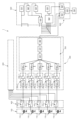
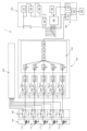
- FIG. 1 shows a schematic block diagram of a phased array sensor 1 according to this embodiment.
- the phased array sensor 1 includes: - The first to nth (n is an integer of 2 or more) non-resonant aerial ultrasonic transducers 110 (first to fifth transducers 110-1 to 110-5 in FIG. 1) are arranged at predetermined intervals.
- a transducer array 100 - a transmission side unit 200 capable of supplying a drive voltage signal to each of the first to n-th transducers 110; - a receiving side unit 300 that processes a received voltage signal generated by each of the first to nth transducers 110 in response to reception of ultrasonic waves; - a switching unit 400 capable of switching between an ultrasonic transmitting operating state and an ultrasonic receiving operating state of the transducer array 100; - A control device 500 that controls the sending unit 200, the receiving unit 300, and the switching unit 400; - A detection device 600 that detects the position of an obstacle based on information regarding the driving voltage signal from the control device 500 and information regarding the received voltage signal from the receiving unit 300 is provided.
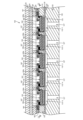
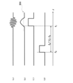
- FIG. 2 shows a longitudinal side view of the transducer array.
- FIG. 3 shows an end view of the transducer array taken along line III-III in FIG. 2. Note that in FIG. 3, some of the constituent members of the transducer array are omitted for ease of understanding.
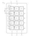
- the transducer array 100 has three transducer rows 105-1 to 105-3. -1 to 105-3, five first to fifth transducers 110 are arranged in series at predetermined intervals. Note that in FIG. 1, one row of five transducers 110 is illustrated.
- the transducer 110 is of a non-resonant type that effectively generates ultrasonic waves using a drive voltage having a frequency lower than the frequency of the lowest-order resonance mode of the transducer 110.
- the transducer array 100 includes, as main components, a rigid support plate 120 having a first surface 121 on one side in the thickness direction and a second surface 122 on the other side in the thickness direction; a flexible resin film 130 having a first surface 131 on one side in the thickness direction and a second surface 132 on the other side in the thickness direction, the second surface 132 being fixed to the first surface 121 of the support plate 120; first to nth (five in the figure) piezoelectric elements 140 fixed to the first surface 131 of the flexible resin film 130, the first to nth piezoelectric elements 140 and the flexible resin Corresponding portions of the membrane 130 form the first to nth transducers 110.
- the support plate 120 has the same number of piezoelectric elements 140 (in this embodiment, 3 rows x 5 pieces) opened on the first surface 121 of the support plate 120.
- recesses 125 the first end of which is opened at the bottom surface of the plurality of recesses 125, and the second end of the other end is opened into the second surface 122 of the support plate 120.
- the same number of waveguides 127 as the recesses 125 are provided.
- the waveguide 127 has a cylindrical shape with an opening width smaller than that of the recess 125 and the same opening width throughout the thickness direction.
- the support plate 120 can be made of various rigid members, and can be made of a metal such as stainless steel, or preferably a ceramic material such as SiC or Al2O3, which has a lower density and higher Young's modulus than metal. can.
- the support plate 120 integrally includes a portion where the plurality of recesses 125 are formed and a portion where the plurality of waveguides 127 are formed.
- the support plate 120 is made of a single plate, it is also possible to make the support plate 120 a laminated structure.
- first plate in which the plurality of recesses 125 are formed
- second plate that is separate from the first plate and has a large thickness. It is also possible to form the support body 120 by fixing the second plate body in which the plurality of waveguides 127 are formed in a laminated state in the thickness direction.
- the flexible resin film 130 is fixed to the first surface 121 of the support plate 120 so as to cover the plurality of recesses 125.
- the flexible resin film 130 is made of an insulating resin such as polyimide and has a thickness of 20 ⁇ m to 100 ⁇ m, for example.
- the flexible resin film 130 is fixed to the support plate 120 using various methods such as adhesive or thermocompression bonding.
- the piezoelectric element 140 is formed of the flexible resin so that its central region overlaps with the corresponding recess 125 and its peripheral region overlaps with the first surface 121 of the support plate 120. It is fixed to the first surface 131 of the membrane 130.
- FIG. 4(a) shows a plan view of the piezoelectric element 140. Further, FIG. 4(b) shows a cross-sectional view taken along the line IV-IV in FIG. 4(a).
- the piezoelectric element 140 includes a piezoelectric element body 142 and a pair of first and second electrodes, and is configured to expand and contract when a voltage is applied between the first and second electrodes.
- the piezoelectric element 140 is of a laminated type. Compared to a single-layer piezoelectric element, a laminated piezoelectric element can increase the electric field strength when the same voltage is applied, and can increase the expansion/contraction displacement per applied voltage.
- the piezoelectric element 140 includes a piezoelectric element main body 142 formed of a piezoelectric material such as lead zirconate titanate (PZT), a first piezoelectric portion 142a on the upper side of the piezoelectric element main body 142 in the thickness direction, An inner electrode 144 partitioning the second piezoelectric portion 142b on the lower side, an upper electrode 146 fixed to a part of the upper surface of the first piezoelectric portion 142a, and a lower electrode fixed to the lower surface of the second piezoelectric portion 142b.
- PZT lead zirconate titanate
- the electrode connecting member 145 has one end electrically connected to the lower electrode 147 and the other end insulated from the upper electrode 146 and the inner electrode 34 and accessible on the upper surface of the first piezoelectric portion 32a. It has a lower electrode connecting member 148 forming a lower electrode terminal 147T.
- the outer electrode formed by the upper surface electrode 146 and the lower surface electrode 147 acts as one of the first and second electrodes
- the inner electrode 144 acts as the other of the first and second electrodes.
- the first and second piezoelectric portions 142a and 142b have the same polarization direction in the thickness direction, so that a predetermined voltage is applied between the outer electrode and the inner electrode 144.
- a predetermined voltage is applied between the outer electrode and the inner electrode 144.
- electric fields are applied to the first and second piezoelectric parts 142a and 142b in opposite directions with respect to each other.
- the upper surface electrode 146 and the lower surface electrode 147 are insulated from each other, so when creating the piezoelectric element 140, a voltage is applied between the upper surface electrode 146 and the lower surface electrode 147. By doing so, the polarization directions of the first and second piezoelectric parts 142a and 142b can be made the same.
- the piezoelectric element 140 and the flexible resin film 130 supporting the piezoelectric element 140 generate ultrasonic waves in response to the application of a driving voltage signal, and receive ultrasonic waves. It acts as a transducer 110 that generates a received voltage signal in response.
- the transducer 110 is configured such that the frequency of the lowest order resonance mode of flexural vibration is higher than the frequency (drive frequency) of the voltage signal applied to the piezoelectric element 140.
- a plurality of transducers 110 formed by the plurality of piezoelectric elements 140 are required. It is necessary to precisely control the phase of the sound waves emitted from the
- the piezoelectric elements are expanded and contracted against the rigidity of the rigid support plate, thereby It is necessary to flexibly vibrate the vibrating body formed by the piezoelectric element and the rigid support plate with a predetermined amplitude to ensure the magnitude of the generated sound pressure.
- the frequency response of the flexural vibration of the transducer formed by the piezoelectric element to the voltage applied to the piezoelectric element has a phase that changes significantly near the resonant frequency of the transducer.
- the ultrasonic transducer array 100 has a plurality of recesses 125 opened in the first surface 121 and a first end portion having an opening width smaller than the opening width of the recesses 125.
- the rigid support plate 120 is provided with a plurality of waveguides 127 that are opened at the bottom of the recess 125 and whose second ends are opened at the second surface 122;
- the flexible resin film 130 is fixed to the first surface 121 of the plate 120 so that the central region overlaps the corresponding recess 125 and the peripheral region overlaps the first surface 121 of the support plate 120 in plan view. and the plurality of piezoelectric elements 140 fixed to the first surface 131 of the flexible resin film 130.
- the resonant frequency of the flexural vibration of the transducer 110 formed by the piezoelectric element 140 is set to be higher than the driving frequency of the voltage signal applied to the piezoelectric element 140, the A sufficient vibration amplitude of the transducer 110 can be ensured.
- the resonant frequency of the transducer 110 is higher than the drive frequency of the piezoelectric element 140, even if there is "variation" in the resonant frequency among the plurality of transducers 110, the plurality of transducers 110 There is no significant difference in the phase of the frequency response of the flexural vibration. Therefore, the phase of the sound waves generated by the plurality of transducers 110 can be precisely controlled.
- the frequency of the ultrasonic waves emitted by the transducer 110 formed by the piezoelectric element 140 must be set to a low frequency of about 30 to 50 kHz. There is a need to.
- the resonant frequency of the transducer 110 is set to a sufficiently higher resonant frequency (for example, 70 kHz) than the drive frequency (30 to 50 kHz) of the transducer 110, it is better to increase the vertical and horizontal dimensions of the piezoelectric element 140 in plan view. However, the sound pressure of the ultrasonic waves generated by the transducer 110 can be increased.
- the arrangement pitch of the plurality of transducers 110 needs to be set to 1/2 or less of the wavelength ⁇ of the ultrasonic waves emitted by the transducers 110.
- the vertical and horizontal dimensions of the piezoelectric element 140 in plan view are preferably 3.0 mm or more from the viewpoint of ensuring sound pressure, and 4.0 mm or less from the viewpoint of suppressing the generation of grating lobes.
- the piezoelectric element 140 has a square shape in a plan view, but instead, the piezoelectric element 140 has a shape in a plan view such that the maximum value of the vertical and horizontal dimensions in a plan view is 4. It is also possible to have a rectangular shape including a rectangle with a diameter of 30 mm or less, a circular shape with a diameter of 4.0 mm or less, or an elliptical shape with a major axis of 4.0 mm or less.
- the opening width of the recess 125 is such that the frequency of the lowest resonance mode of the flexural vibration of the transducer 110 formed by the piezoelectric element 140 and the flexible resin film 130 is the frequency of the voltage signal applied to the piezoelectric element 140 ( (driving frequency).
- the recess 125 is formed so that the overlapping width of the peripheral edge region of the piezoelectric element 140 and the support plate 120 in plan view is 0.05 mm to 0.1 mm over the entire circumference of the piezoelectric element 140.
- the shape is similar to that of the piezoelectric element 140 in plan view.
- the recess 125 preferably has a square shape in a plan view with a side of 3.8 mm to 3.9 mm
- the recess 125 preferably has a circular shape in a plan view with a diameter of 3.8 mm to 3.9 mm.
- the rigid support plate 120 is provided with the openings 125 at 15 locations (3 ⁇ 5), and the flexible resin film 130 is The 15 piezoelectric elements 140 are arranged so as to overlap each other with the 15 openings 125 in a plan view when sandwiched between them.
- fifteen transducers 110 are provided, it is understood that the present invention is not limited to such a configuration. In order to sharpen the directivity of the radiated sound waves and increase the intensity, it is desirable to arrange more than 3 ⁇ 5 transducers 110.
- the transducer array 100 further includes a lower sealing plate 150 and a wiring assembly 180.
- the lower sealing plate 150 has a plurality of piezoelectric element openings each having a size that surrounds the plurality of piezoelectric elements 140, and in a plan view, the plurality of piezoelectric elements 140 have a plurality of piezoelectric element openings.
- the first surface 131 of the flexible resin film 130 is fixed to the first surface 131 of the flexible resin film 130 by adhesive or thermocompression bonding so as to be located inside the flexible resin film 130 .
- the thickness of the lower sealing plate 150 is greater than the thickness of the piezoelectric element 140, and the lower sealing plate 150 is fixed to the first surface 131 of the flexible resin film 130. , the first surface of the lower sealing plate 150 is further away from the flexible resin film 130 than the upper surface electrode 146, the lower surface electrode terminal 147T, and the inner electrode terminal 144T (see FIG. 4) of the piezoelectric element 140. are spaced apart.
- the lower sealing plate 150 is formed of a rigid member such as metal such as stainless steel, carbon fiber reinforced plastic, or ceramics.
- the lower sealing plate 150 seals the sides of the piezoelectric element group including the plurality of piezoelectric elements 140, and acts as a base to which the wiring assembly 180 is fixed.
- the wiring assembly 180 transmits the drive voltage signal supplied from the transmission side unit 200 via the switching unit 400 to the first to n-th transducers 110, and A signal transmission path is formed for transmitting a received voltage signal generated by the switching unit 400 to the receiving unit 300 via the switching unit 400.
- the wiring assembly 180 includes an insulating base layer 182 fixed to the lower sealing plate 150 with an adhesive or the like, a conductor layer 185 fixed to the base layer 182, and a conductor layer 185 fixed to the base layer 182. It has an insulating cover layer 187 surrounding the layer 185.
- the base layer 182 and the cover layer 187 are made of, for example, an insulating resin such as polyimide.
- the conductor layer 185 is made of, for example, a conductive metal such as Cu.
- the exposed portion of Cu forming the conductor layer 185 may be plated with Ni/Au.
- the conductor layer 185 is connected to the first electrode (outer electrodes 146 and 147 in this embodiment) and the second electrode (inner electrode 144 in this embodiment) of the piezoelectric element 140. It includes a first wiring 185a and a second wiring 185b that are connected to each other.
- the upper surface electrode 146 and the lower surface electrode 147 act as the first electrode, and the inner electrode 144 acts as the second electrode.
- the first wiring 185a is electrically connected to both a part of the upper surface electrode 146 and the lower surface electrode terminal 147T, for example, by a conductive adhesive or solder.
- the second wiring 185b is electrically connected to the inner electrode terminal 144T by, for example, a conductive adhesive or solder.
- the transducer array 100 further includes an upper sealing plate 160 fixed to the upper surface of the lower sealing plate 150 and the wiring assembly 180 via a flexible resin 155.
- the upper sealing plate 160 has openings 162 at positions corresponding to each of the plurality of piezoelectric elements 140.
- the upper sealing plate 160 is formed of, for example, metal such as stainless steel, carbon fiber reinforced plastic, ceramics, etc. with a thickness of 0.1 mm to 0.3 mm.
- the transducer array 100 further includes a sound absorbing material 165 fixed to the upper surface of the upper sealing plate 160 by adhesive or the like so as to cover the plurality of openings 162 of the upper sealing plate 160.
- the sound absorbing material 165 is made of, for example, silicone resin or other foamable resin with a thickness of about 0.3 mm to 1.5 mm.
- the transducer array 100 further includes a reinforcing plate 170 fixed to the upper surface of the sound absorbing material 165 by adhesive or the like.
- the reinforcing plate 170 is made of, for example, metal such as stainless steel, carbon fiber reinforced plastic, ceramics, etc. and has a thickness of about 0.2 mm to 0.5 mm.
- FIG. 5 shows a schematic block diagram of the control device 500 and the transmitting unit 200.
- FIG. 6 shows a schematic explanatory diagram of the operation when the transducer array 100 emits ultrasonic waves in response to the drive voltage signal supplied from the transmission side unit 200.
- ⁇ is the azimuth angle of the ultrasonic waves emitted from the transducer array 100
- d is the arrangement interval between adjacent transducers
- c is the speed of sound.
- the control device 500 includes a clock signal generation circuit 510 that generates a clock signal with a cycle of, for example, 0.1 ⁇ sec to determine the operation timing of a digital circuit, and a clock signal generated by the clock signal generation circuit 510.
- a time unit setting counter circuit 520 that reduces the frequency of the clock signal to an appropriate time step, for example, a 0.1 msec period for setting the burst wave period; and a burst wave drive that transmits to the first to n-th transducers 110.
- the total time of the burst wave drive voltage signal to be generated is determined.
- an active counter circuit 540 that outputs an active pulse signal with a time width corresponding to the width;
- an azimuth angle control section 550 that outputs an azimuth signal indicating the azimuth angle ⁇ of the ultrasonic waves emitted by the transducer array 100; It has a delay time control section 560 that calculates a delay time ⁇ based on the azimuth signal sent from the angle control section 550 and outputs a delay control signal.
- the transmitting unit 200 includes first to nth signal generating means 220-1 to 220-n for generating drive voltage signals for the first to nth transducers 110, respectively.
- the transmission signal generating device 210 including the first to fifth signal generating means 220-1 to 220-5 in the figure and the driving voltage signals generated by the first to nth signal generating means 220 are It has first to nth transmission side channels 250-1 to 250-n (in the illustration, first to fifth transmission side channels 250-1 to 250-5) that transmit data toward the first to nth transducers 110. are doing.
- the signal generating means 220 includes a frequency divider 222, a delay time counter circuit 224, and a wave number counter circuit 226.
- the frequency divider 222 divides the frequency of the clock signal from the clock signal generation circuit 510 to generate a rectangular burst wave drive voltage signal of a predetermined frequency.
- the delay time counter circuit 224 When activated by the active pulse signal from the active counter circuit 540, the delay time counter circuit 224 controls the frequency divider 222 according to the delay time specified by the delay control signal from the delay time control section 560. A start signal pulse is sent to the frequency divider 222, whereby the frequency divider 222 starts outputting a rectangular burst wave drive voltage signal.
- the wave number counter circuit 226 sends a stop signal pulse to the frequency divider 222 when the wave number of the rectangular burst wave drive voltage signal output from the frequency divider 222 reaches a predetermined wave number.
- the transmitter unit 200 further includes first to n-th channels inserted into the first to n-th transmitter channels 250-1 to 250-n, respectively. It has transmission side filters 260-1 to 260-n (in the illustration, first to fifth transmission side filters 260-1 to 260-5).
- the transmission side filter 260 is configured to remove at least the resonance frequency component of the transducer 110 while allowing the drive frequency component to pass.
- the transmission side filter 260 is a low-pass filter or a band-pass filter configured to remove the resonant frequency component of the transducer while allowing the passage of the driving frequency component, or a filter configured to remove only the resonant frequency component of the transducer 110. It can be a band-stop filter that removes pinpoint signals.
- the bandpass filter is preferably configured to pass only frequency components of ⁇ 10% of the drive frequency.
- the resonant frequency (for example, 70 kHz) of the non-resonant transducer 110 can be effectively passed through while effectively passing the driving frequency (30 to 50 kHz) required to detect an object several meters away. Components can be effectively removed or reduced.
- f is the frequency of the ultrasonic wave
- ⁇ f is the frequency fluctuation due to the Doppler effect
- c is the speed of sound.
- the bandpass filter used as the transmission side filter 260 is configured to pass only the frequency components of ⁇ 1% of the drive frequency, the influence of the Doppler effect can be reduced as much as possible.
- the rectangular burst wave driving voltage signal is converted into a sine wave burst driving voltage signal having the same fundamental frequency (see FIG. 6).
- the transmitter unit 200 includes a power amplifier circuit 270 inserted into the transmitter channel 250 on the downstream side of the transmitter filter 260 in the signal transmission direction. ing.
- the power amplifier circuit 270 includes a buffer circuit 272 and an amplifier circuit 274.
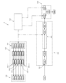
- FIG. 7 shows a schematic block diagram of the receiving unit 300 and the control device 500. Further, FIG. 8 shows a schematic operational explanatory diagram when the receiving unit 300 processes a received voltage signal generated by the transducer array 100 in response to reception of ultrasonic waves.
- the receiving side unit 300 is a first to nth receiving unit capable of receiving received voltage signals generated by the first to nth transducers 110-1 to 110-n, respectively.
- channels 310-1 to 310-n in the illustration, the first to fifth receiving channels 310-1 to 310-5) and the first to nth receiving channels 310-1 to 310-n, respectively.
- the first to nth receiving side filters 320-1 to 320-n in the illustration, the first to fifth receiving side filters 320-1 to 320-5) and the first to nth receiving side channels 320- 1 to 320-n.
- the receiving filter 320 is configured to remove at least the resonant frequency component of the transducer while allowing the drive frequency component to pass.
- the reception side filter 320 may be a low-pass filter or a band-pass filter configured to remove the resonant frequency component of the transducer while allowing the passage of the drive frequency component, or a filter configured to remove only the resonant frequency component of the transducer.
- a band-rejection filter is used that eliminates at a point.
- the bandpass filter is preferably configured to pass only frequency components of ⁇ 10% of the drive frequency.
- the component of the resonant frequency (for example, 70 kHz) of the non-resonant transducer can be transmitted. can be effectively removed or reduced.
- the bandpass filter used as the receiving side filter 320 is preferably configured to pass only frequency components of ⁇ 1% of the driving frequency.
- the receiving side unit 300 includes the first to nth receiving filters 320-1 to 320-n downstream of the first to nth receiving filters 320-1 to 320-n in the signal transmission direction.
- First to n-th low noise amplification circuits 330-1 to 330-n (in the illustration, first to fifth low-noise amplification circuits 330-1 to 330 -5).
- the received signal processing device 350 has first to nth delays that can delay the received voltage signals of the first to nth receiving channels 310-1 to 310-n by corresponding predetermined times. Adding the output signals of the circuits 360-1 to 360-n (in the illustration, the first to fifth delay circuits 360-1 to 360-5) and the first to n-th delay circuits 360-1 to 360-n. It has an adder circuit 370 and a detector 380 that generates a pulse signal having a width corresponding to the duration of the added received voltage signal (time width of the entire signal) generated by the adder circuit 370.
- the delay time of the first to n-th delay circuits 360-1 to 360-n is determined by the delay time of the first to nth delay circuits 360-1 to 360-n. It is set so that only the received voltage signal due to the return ultrasonic wave at the azimuth angle ⁇ reflected from an obstacle existing at the azimuth angle ⁇ at the time of emission and returned to coincide with the time axis.
- the first to n-th delay circuits 360-1 to 360-n each receive signals from the first to n-th receiving channels 310-1 to 310-n sent from the delay time control section 560. Each received voltage signal is delayed by a delay time based on the delay control signal.
- the delay time of the fifth delay circuit 360-5 that delays the received voltage signal from the fifth transducer 110-5 is set to zero, and the received voltage signal from the fourth transducer 110-4 is set to zero.
- the delay time of the fourth delay circuit 360-4 that delays the signal is determined based on the received voltage signal from the fifth transducer 110-5, the arrangement interval d between the adjacent fifth transducer 110-5, and the azimuth angle. It is set to the time ⁇ calculated based on ⁇ and the speed of sound c.
- the delay time of the third delay circuit 360-3 that delays the received voltage signal from the third transducer 110-3 is a time ⁇ with respect to the received voltage signal from the adjacent fourth transducer 110-4. , the time is set to 2 ⁇ based on the received voltage signal from the fifth transducer 110-5.
- the delay time of the second delay circuit 360-2 that delays the received voltage signal from the second transducer 110-2 is the time ⁇ , with respect to the received voltage signal from the adjacent third transducer 110-3. That is, based on the received voltage signal from the fifth transducer 110-5, the time is set to 3 ⁇ , and the delay time of the first delay circuit 360-1 that delays the received voltage signal from the first transducer 110-1 is , is set to a time ⁇ with respect to the received voltage signal from the adjacent second transducer 110-2, that is, a time 4 ⁇ with respect to the received voltage signal from the fifth transducer 110-5.
- the adder circuit 370 receives the received voltage signals of the first to n-th receiving channels 310-1 to 310-n whose time axes are matched by the first to n-th delay circuits 360-1 to 360-n. Add.
- the reflected ultrasonic waves reflected from the obstacle are detected in other directions. It is possible to detect a virtual image based on multiple reflected ultrasound waves that are reflected back from other obstacles in the area.
- the first to n-th transducers 110-1 to 110-n are used both for ultrasonic transmission and ultrasonic reception. It is possible to match only the received voltage signal due to the return ultrasonic wave at the azimuth angle ⁇ , which is emitted towards the angle ⁇ , reflected from an obstacle present at the azimuth angle ⁇ , and returned to the time axis, and detects a virtual image. can be effectively avoided.
- the detector 380 is an envelope detector that extracts a waveform connecting the plus-side vertices of each period in the added received voltage signal generated by the adder circuit 370.
- FIG. 9(a) shows the waveform of the output signal from the adder 370
- FIG. 9(b) shows the waveform of the output signal from the detector 380 (in this embodiment, the envelope detector).
- the received signal processing device 350 includes a signal processing section 375 between the adder 370 and the detector 380 in the signal transmission direction. .
- the signal processing unit 375 may include a variable gain amplifier (not shown), a bandpass filter (not shown), and a logarithmic amplifier (not shown).
- variable gain amplifier increases the amplification as the time difference between the emission timing of the ultrasonic waves from the transducer array 100 due to the drive voltage signal from the transmitting side unit 200 and the reception timing of the returned ultrasonic waves by the transducer array 100 increases. It is configured so that the gain is large.
- variable gain amplifier is provided in consideration of the fact that the more distant the ultrasonic wave returns from an obstacle, the greater the attenuation of the acoustic wave and the smaller the amplitude of the received voltage signal.
- the bandpass filter is configured to pass only the driving frequency component, for example, only the frequency component of 30 kHz to 50 kHz.
- the logarithmic amplifier is configured to have a small gain for signals with small amplitude and a large gain for signals with large amplitude.
- the detection device 600 includes a time difference detection section 610, a direction detection section 620, and a position detection section 630.
- the azimuth detection unit 620 is configured to recognize the azimuth angle ⁇ at which the transducer array 100 emits the ultrasonic waves based on the azimuth information sent from the control device 500.
- the position detection unit 630 identifies the position of the obstacle based on the distance to the obstacle calculated based on the detection result of the time difference detection unit 610 and the azimuth of the obstacle recognized by the azimuth detection unit 620. do.
- the phased array sensor 1 further includes a display device 700 that displays position information of the obstacle identified by the detection device 600. There is.
- the switching unit 400 has first to nth changeover switches 410-1 to 410-n (first to fifth changeover switches 410-1 to 410-5 in the figure). have.
- the first to nth changeover switches 410-1 to 410-n switch the first to nth transducers 110-1 to 100-n, respectively, based on the control signal from the control device 500.
- FIG. 5 shows the transmission states of the first to nth changeover switches 410-1 to 410-n
- FIG. 7 shows the reception states of the first to nth changeover switches 410-1 to 410-n.
- the control device 500 causes the first to nth changeover switches 410-1 to 410-n to be in the transmission state to transmit drive voltage signals to the first to nth transducers 110-1 to 110-n. Immediately after the end, the first to n-th changeover switches 410-1 to 410-n are switched to the receiving state.
- the ultrasonic phased array sensor 1 has the following effects. That is, the transducer 110 is of a non-resonant type that can effectively emit ultrasonic waves even when using a burst wave drive voltage signal having a sufficiently lower drive frequency (for example, 40 kHz) than the resonant frequency (for example, 70 kHz). Even if a drive voltage with a drive frequency sufficiently lower than the resonant frequency of the transducer 110 is applied to the transducer 110 to cause the transducer to emit an ultrasonic wave, the burst wave drive voltage signal is a rectangular wave or rectangular wave. In the case of a waveform close to a wave, not only vibrations at the drive frequency but also vibrations at the resonant frequency of the transducer 110 occur.
- a burst wave drive voltage signal having a sufficiently lower drive frequency (for example, 40 kHz) than the resonant frequency (for example, 70 kHz).
- the generated ultrasonic waveform is distorted, and the damped vibration at the resonant frequency of the transducer 110 after the application of the drive voltage signal is also increased and becomes longer.
- the damped vibration at the resonant frequency of the transducer 110 is the vibration caused by the ultrasonic waves reflected back from the transducer 110 from an obstacle after the transducer array 100 is switched from the transmitting operating state to the receiving operating state. This will greatly impair the accuracy of detecting the position of the obstacle.
- the transducer is allowed to pass through the first to n-th transmission side channels 250-1 to 250-n while allowing the drive frequency components to pass through.
- the first to n-th transmitting side filters 260-1 to 260-n that remove the resonance frequency components of 110 are inserted.
- a burst wave driving voltage converted from a rectangular wave to a sine wave is applied to the transducer 110, and resonance vibration of the transducer 110 is effectively prevented or reduced.
- the above-mentioned disadvantages caused by resonance vibration can be effectively prevented or reduced.
- a sinusoidal burst wave drive voltage signal is applied to the transducer 110, but even in this case, the voltage signal is compared to a rectangular burst wave drive voltage signal. Although the vibration is small, resonant vibration may occur in the transducer 110.
- the transducer is allowed to pass through the first to n-th receiving side channels 310-1 to 310-n while allowing the drive frequency components to pass through.
- the first to n-th receiving side filters 320-1 to 320-n that remove the resonance frequency components of 110 are inserted.
- the received voltage signal is amplified by an amplifier circuit
- the resonance of the transducer 110 The adverse effects of saturation of the amplifier due to signals based on damped oscillations at frequencies can be effectively prevented or reduced.
- FIG. 10 shows a schematic block diagram of an ultrasonic phased array sensor 1' including a receiving unit 300' according to a modified example instead of the receiving unit 300.
- the same members as in this embodiment are given the same reference numerals, and the description thereof will be omitted as appropriate.
- the receiving side unit 300' Compared to the receiving side unit 300, the receiving side unit 300' has first to nth delay circuits 360-1 to 360-n (on the upstream side in the signal transmission direction), respectively. It has D converters 390-1 to 390-n.
- the receiving unit 300' is configured to process the delay circuits 360-1 to 360-n and subsequent received voltage signals by digital signal processing.
- the detector 380 is a quadrature detector.
- the ultrasonic phased array sensor 1' equipped with the receiving unit 300' can also obtain the same effects as the ultrasonic phased array sensor 1 according to the present embodiment.
- FIG. 11 shows a schematic block diagram of the phased array sensor 2 according to this embodiment.
- the same members as those in the first embodiment are designated by the same reference numerals, and detailed explanation thereof will be omitted as appropriate.
- the operating states of the first to n-th transducers 110 can be switched between the ultrasonic transmission operating state and the ultrasonic transmitting state by the first to n-th changeover switches 410.
- the device is configured to switch to a sound wave reception operating state.
- the first to nth transducers 110 act only for transmitting ultrasonic waves, and the first to nth transducers 110 are It has a single airborne ultrasound transducer 112 for reception only.
- the phased array sensor 2 differs from the sensor 1 according to the first embodiment in that the switching unit 400 is deleted, the receiving transducer 112 is included, and the receiving side unit 300 is replaced with the receiving transducer 112. It has a receiving side unit 302 at.
- the phased array sensor 2 includes the first to n-th transducers 110-1 to 110-n (in the illustration, the first to fifth transducers 110-1 to 110-n).
- 110-5) is the transducer array 100 used exclusively for ultrasonic transmission, the transmission signal generator 210, and the first to n-th transmission side channels 250-1 to 250-n (in the illustration, the first - fifth transmitting side channels 250-1 to 250-5) and the first to nth transmitting side filters 260-1 to 260-n (in the illustration, the first to fifth transmitting side filters 260-1 to 260- 5), and a single ultrasonic wave transmitter capable of receiving return ultrasonic waves transmitted from the first to n-th transducers 110-1 to 110n acting as transmission-only transducers and reflected back from obstacles to be detected.
- the receiving aerial ultrasonic transducer 112 the receiving channel 310 capable of receiving the receiving voltage signal generated by the receiving transducer 112; and the receiving filter 320 inserted into the receiving channel 310;
- the time difference between the control device 500 and the transmission timing signal based on the drive voltage signal sent from the control device 500 and the reception timing signal based on the reception voltage signal sent from the detector 380 and the transmission timing signal sent from the control device 500.
- the detection device 600 detects the position of an obstacle based on the received azimuth information.
- the receiving transducer 112 may be of a non-resonant type similar to the transducer 110 acting as a transmitting transducer, or alternatively, the receiving transducer 112 may be of a non-resonant type, in which the transmitting signal is generated by the transmitting signal generator 210. It is also possible to use a resonant type that performs resonance vibration depending on the drive frequency of the drive voltage signal.
- the receiving side filter 320 is configured to remove at least a resonant frequency component of the receiving transducer 112 while allowing passage of a driving frequency component. be done.
- the receiving filter 320 is a noise removal filter.
- the received signal processing device 352 includes the signal processing section 375 upstream of the detector 380 in the signal transmission direction.
- the signal processing unit 375 may include a variable gain amplifier (not shown), a bandpass filter (not shown), and a logarithmic amplifier (not shown).
- FIG. 12 shows a schematic block diagram of the phased array sensor 3 according to this embodiment.
- the same members as in the first and second embodiments are designated by the same reference numerals, and detailed explanation thereof will be omitted as appropriate.
- the phased array sensor 3 differs from the phased array sensor 2 according to the second embodiment in that the phased array sensor 3 functions as a transmitting transducer instead of the single receiving transducer 112. It has first to nth receiving transducers 112-1 to 112-n corresponding to the first to nth transducers 110-1 to 110-n, respectively, and the receiving side unit 302 is replaced by the receiving side unit 302. It has a unit 300.
- the phased array sensor 3 includes the first to nth transducers 110-1 to 110-n (in the illustration, the first to nth transducers 110-1 to 110-n) are used exclusively for ultrasonic transmission.
- the transducer array 100 having five transducers 110-1 to 110-5); 1 to 5 transmission side channels 250-1 to 250-5), and the first to nth transmission side filters 260-1 to 260-n (in the illustration, the first to fifth transmission side filters 260-1 to 260-n). 260-5), and a receiving transducer including the first to nth receiving transducers 112-1 to 112-n (in the illustration, the first to fifth receiving transducers 112-1 to 112-5).
- the first to n-th receiving channels 310-1 to 310-n in the illustration, the first to fifth receiving channels 310-1 to 310-5
- the first to n-th receiving channels side filters 320-1 to 320-n in the illustration, the first to fifth receiving side filters 320-1 to 320-5
- the first to nth receiving side channels 310-1 to 310-n in the illustration, the first to fifth receiving side filters 320-1 to 320-5
- the first to n-th delay circuits 360-1 to 360-n (in the illustration, the first to fifth delay circuits 360-1 to 360-5) each capable of delaying a voltage signal by a predetermined time;
- the received signal includes the addition circuit 370 that adds the output signals of the n delay circuits 360-1 to 360-n, and the detector 380 that generates a signal having a width corresponding to the duration of the output signal of the addition circuit 370.
- the detection device 600 detects the position of an obstacle based on the time difference of the reception timing signal based on the reception voltage signal sent from the control device 500 and the azimuth information sent from the control device 500.
- the receiving transducers 112-1 to 112-n can be of non-resonant type, and unlike this, the driving voltage generated by the transmitting signal generator 210 It is also possible to use a resonant type that performs resonant vibration depending on the driving frequency of the signal.
- the receiving filters 320-1 to 320-n allow at least the receiving transducer to pass through while allowing the driving frequency component to pass through. It is configured to remove resonance frequency components of the inducers 112-1 to 112-n.
- the reception side filters 320-1 to 320-n are noise removal filters.
- the phased array sensor 3 according to the present embodiment can more effectively avoid virtual image detection than the phased array sensor 2 according to the second embodiment.
- the phased array sensor 2 since the phased array sensor 2 according to the second embodiment has only the single reception transducer 112, the transmission transducer array 100 emits radiation at the azimuth angle ⁇ , and the radiation is emitted at the azimuth angle ⁇ . It is not possible to detect only the return ultrasonic waves at the azimuth angle ⁇ that are reflected from existing obstacles and returned.
- the reflected ultrasonic wave reflected from the obstacle is reflected by another obstacle existing in another direction.
- the first to n-th transducers 110-1 to 110- act for transmission, similar to the phased array sensor 1 according to the first embodiment. Only the received voltage signal due to the return ultrasonic wave at the azimuth angle ⁇ reflected from an obstacle existing at the azimuth angle ⁇ from which the ultrasonic wave was emitted by the transducer array 100 having n and returned is matched with respect to the time axis. Detection of virtual images can be effectively avoided.
- a receiving unit (not shown) configured to perform digital signal processing is used instead of the receiving unit 300. ).
- Ultrasonic phased array sensor 100 Transducer array 102 Receiving transducer array 110 Transducer 112 Receiving transducer 210 Transmitting signal generator 220 Signal generating means 250 Transmitting side channel 260 Transmitting side filter 310 Receiving side channel 320 Receiving side Filter 330 Low noise amplification circuits 350, 352 Received signal processing device 410 Changeover switch 500 Control device
Landscapes
- Physics & Mathematics (AREA)
- General Physics & Mathematics (AREA)
- Engineering & Computer Science (AREA)
- Chemical & Material Sciences (AREA)
- Immunology (AREA)
- Biochemistry (AREA)
- General Health & Medical Sciences (AREA)
- Analytical Chemistry (AREA)
- Life Sciences & Earth Sciences (AREA)
- Pathology (AREA)
- Health & Medical Sciences (AREA)
- Radar, Positioning & Navigation (AREA)
- Remote Sensing (AREA)
- Computer Networks & Wireless Communication (AREA)
- Ceramic Engineering (AREA)
- Acoustics & Sound (AREA)
- Measurement Of Velocity Or Position Using Acoustic Or Ultrasonic Waves (AREA)
Priority Applications (3)
| Application Number | Priority Date | Filing Date | Title |
|---|---|---|---|
| US18/865,304 US20250369929A1 (en) | 2022-05-13 | 2022-05-13 | Ultrasonic phased array sensor |
| PCT/JP2022/020234 WO2023218644A1 (ja) | 2022-05-13 | 2022-05-13 | 超音波フェイズドアレイセンサー |
| JP2023507444A JP7293521B1 (ja) | 2022-05-13 | 2022-05-13 | 超音波フェイズドアレイセンサー |
Applications Claiming Priority (1)
| Application Number | Priority Date | Filing Date | Title |
|---|---|---|---|
| PCT/JP2022/020234 WO2023218644A1 (ja) | 2022-05-13 | 2022-05-13 | 超音波フェイズドアレイセンサー |
Publications (1)
| Publication Number | Publication Date |
|---|---|
| WO2023218644A1 true WO2023218644A1 (ja) | 2023-11-16 |
Family
ID=86772550
Family Applications (1)
| Application Number | Title | Priority Date | Filing Date |
|---|---|---|---|
| PCT/JP2022/020234 Ceased WO2023218644A1 (ja) | 2022-05-13 | 2022-05-13 | 超音波フェイズドアレイセンサー |
Country Status (3)
| Country | Link |
|---|---|
| US (1) | US20250369929A1 (enExample) |
| JP (1) | JP7293521B1 (enExample) |
| WO (1) | WO2023218644A1 (enExample) |
Citations (4)
| Publication number | Priority date | Publication date | Assignee | Title |
|---|---|---|---|---|
| JPH02102481A (ja) * | 1988-10-08 | 1990-04-16 | Honda Motor Co Ltd | 超音波誘導装置 |
| WO2011043362A1 (ja) * | 2009-10-07 | 2011-04-14 | 日本電気株式会社 | 超音波送信装置、超音波伝播時間測定システムおよび超音波伝播時間測定方法 |
| JP2016125987A (ja) * | 2015-01-08 | 2016-07-11 | ローム株式会社 | 超音波センサ及びバースト信号の制御方法 |
| US20200340955A1 (en) * | 2019-04-23 | 2020-10-29 | Decision Sciences Medical Company, LLC | Direct sequence spread spectrum coded waveforms in ultrasound imaging |
Family Cites Families (4)
| Publication number | Priority date | Publication date | Assignee | Title |
|---|---|---|---|---|
| US4414482A (en) * | 1981-05-20 | 1983-11-08 | Siemens Gammasonics, Inc. | Non-resonant ultrasonic transducer array for a phased array imaging system using1/4 λ piezo elements |
| GB2268806B (en) * | 1992-07-14 | 1997-02-26 | Intravascular Res Ltd | Methods and apparatus for the examination and treatment of internal organs |
| JP6874647B2 (ja) * | 2017-11-07 | 2021-05-19 | 株式会社デンソー | 送受信制御装置 |
| JP2019100715A (ja) * | 2017-11-28 | 2019-06-24 | キヤノン株式会社 | 超音波センサ |
-
2022
- 2022-05-13 US US18/865,304 patent/US20250369929A1/en active Pending
- 2022-05-13 JP JP2023507444A patent/JP7293521B1/ja active Active
- 2022-05-13 WO PCT/JP2022/020234 patent/WO2023218644A1/ja not_active Ceased
Patent Citations (4)
| Publication number | Priority date | Publication date | Assignee | Title |
|---|---|---|---|---|
| JPH02102481A (ja) * | 1988-10-08 | 1990-04-16 | Honda Motor Co Ltd | 超音波誘導装置 |
| WO2011043362A1 (ja) * | 2009-10-07 | 2011-04-14 | 日本電気株式会社 | 超音波送信装置、超音波伝播時間測定システムおよび超音波伝播時間測定方法 |
| JP2016125987A (ja) * | 2015-01-08 | 2016-07-11 | ローム株式会社 | 超音波センサ及びバースト信号の制御方法 |
| US20200340955A1 (en) * | 2019-04-23 | 2020-10-29 | Decision Sciences Medical Company, LLC | Direct sequence spread spectrum coded waveforms in ultrasound imaging |
Also Published As
| Publication number | Publication date |
|---|---|
| US20250369929A1 (en) | 2025-12-04 |
| JP7293521B1 (ja) | 2023-06-19 |
| JPWO2023218644A1 (enExample) | 2023-11-16 |
Similar Documents
| Publication | Publication Date | Title |
|---|---|---|
| CN102859580B (zh) | 用于触发超声传感器的方法以及超声传感器 | |
| US4217516A (en) | Probe for ultrasonic diagnostic apparatus | |
| JP3556582B2 (ja) | 超音波診断装置 | |
| KR860000380B1 (ko) | 초음파 진단장치 | |
| US4462092A (en) | Arc scan ultrasonic transducer array | |
| US4440025A (en) | Arc scan transducer array having a diverging lens | |
| KR910000233B1 (ko) | 초음파 진단장치 | |
| US4122725A (en) | Length mode piezoelectric ultrasonic transducer for inspection of solid objects | |
| CN102197660A (zh) | 声振子以及图像生成装置 | |
| CN112912184B (zh) | 声变换器和用于运行声变换器的方法 | |
| US4552021A (en) | Electro-sound transducer eliminating acoustic multi-reflection, and ultrasonic diagnostic apparatus applying it | |
| EP0005071B2 (en) | Probe for electronic scanning type ultrasonic diagnostic apparatus | |
| US4414482A (en) | Non-resonant ultrasonic transducer array for a phased array imaging system using1/4 λ piezo elements | |
| WO2023218644A1 (ja) | 超音波フェイズドアレイセンサー | |
| KR100762087B1 (ko) | 초음파 트랜스듀서의 구동방법 | |
| JPWO2023218644A5 (enExample) | ||
| JP7288562B1 (ja) | 超音波トランスデューサーアレイ及び超音波フェイズドアレイセンサー | |
| JP2004033666A (ja) | 超音波探触子および超音波診断装置 | |
| US4497322A (en) | Ultrasonic detection apparatus | |
| JPH1114649A (ja) | 流速測定装置 | |
| JP2023065084A (ja) | 超音波センサー | |
| JP2022011510A (ja) | 超音波デバイス | |
| CN112887881A (zh) | 超声波设备 | |
| JPH0649287Y2 (ja) | 超音波診断装置 | |
| JPH02238799A (ja) | ソーナー用送受波器 |
Legal Events
| Date | Code | Title | Description |
|---|---|---|---|
| ENP | Entry into the national phase |
Ref document number: 2023507444 Country of ref document: JP Kind code of ref document: A |
|
| 121 | Ep: the epo has been informed by wipo that ep was designated in this application |
Ref document number: 22941721 Country of ref document: EP Kind code of ref document: A1 |
|
| NENP | Non-entry into the national phase |
Ref country code: DE |
|
| 122 | Ep: pct application non-entry in european phase |
Ref document number: 22941721 Country of ref document: EP Kind code of ref document: A1 |