WO2023218644A1 - Ultrasonic phased array sensor - Google Patents
Ultrasonic phased array sensor Download PDFInfo
- Publication number
- WO2023218644A1 WO2023218644A1 PCT/JP2022/020234 JP2022020234W WO2023218644A1 WO 2023218644 A1 WO2023218644 A1 WO 2023218644A1 JP 2022020234 W JP2022020234 W JP 2022020234W WO 2023218644 A1 WO2023218644 A1 WO 2023218644A1
- Authority
- WO
- WIPO (PCT)
- Prior art keywords
- transducer
- signal
- receiving
- transducers
- transmission
- Prior art date
Links
- 230000005540 biological transmission Effects 0.000 claims abstract description 77
- 230000007274 generation of a signal involved in cell-cell signaling Effects 0.000 claims abstract description 28
- 238000001514 detection method Methods 0.000 claims abstract description 26
- 230000008054 signal transmission Effects 0.000 claims description 8
- 229920005989 resin Polymers 0.000 description 21
- 239000011347 resin Substances 0.000 description 21
- 238000010586 diagram Methods 0.000 description 16
- 238000007789 sealing Methods 0.000 description 15
- 239000010410 layer Substances 0.000 description 12
- 238000002604 ultrasonography Methods 0.000 description 8
- 239000000853 adhesive Substances 0.000 description 7
- 230000001070 adhesive effect Effects 0.000 description 7
- 230000003321 amplification Effects 0.000 description 6
- 230000001934 delay Effects 0.000 description 6
- 239000002184 metal Substances 0.000 description 6
- 238000003199 nucleic acid amplification method Methods 0.000 description 6
- 239000004020 conductor Substances 0.000 description 5
- 230000000694 effects Effects 0.000 description 5
- 229910001220 stainless steel Inorganic materials 0.000 description 5
- 239000010935 stainless steel Substances 0.000 description 5
- 239000011358 absorbing material Substances 0.000 description 4
- 238000000034 method Methods 0.000 description 4
- 239000004918 carbon fiber reinforced polymer Substances 0.000 description 3
- 230000010355 oscillation Effects 0.000 description 3
- 230000002093 peripheral effect Effects 0.000 description 3
- 230000003014 reinforcing effect Effects 0.000 description 3
- 239000004642 Polyimide Substances 0.000 description 2
- 230000002411 adverse Effects 0.000 description 2
- 239000000919 ceramic Substances 0.000 description 2
- 230000005684 electric field Effects 0.000 description 2
- 229910052451 lead zirconate titanate Inorganic materials 0.000 description 2
- 239000012528 membrane Substances 0.000 description 2
- 230000004048 modification Effects 0.000 description 2
- 238000012986 modification Methods 0.000 description 2
- 230000010287 polarization Effects 0.000 description 2
- 229920001721 polyimide Polymers 0.000 description 2
- 230000005855 radiation Effects 0.000 description 2
- 229910000679 solder Inorganic materials 0.000 description 2
- 238000011144 upstream manufacturing Methods 0.000 description 2
- PNEYBMLMFCGWSK-UHFFFAOYSA-N aluminium oxide Inorganic materials [O-2].[O-2].[O-2].[Al+3].[Al+3] PNEYBMLMFCGWSK-UHFFFAOYSA-N 0.000 description 1
- 230000002238 attenuated effect Effects 0.000 description 1
- 229910010293 ceramic material Inorganic materials 0.000 description 1
- 239000003638 chemical reducing agent Substances 0.000 description 1
- 239000000470 constituent Substances 0.000 description 1
- 230000008602 contraction Effects 0.000 description 1
- 229910052593 corundum Inorganic materials 0.000 description 1
- 230000003111 delayed effect Effects 0.000 description 1
- 239000006185 dispersion Substances 0.000 description 1
- 238000006073 displacement reaction Methods 0.000 description 1
- 239000000284 extract Substances 0.000 description 1
- 239000000411 inducer Substances 0.000 description 1
- HFGPZNIAWCZYJU-UHFFFAOYSA-N lead zirconate titanate Chemical compound [O-2].[O-2].[O-2].[O-2].[O-2].[Ti+4].[Zr+4].[Pb+2] HFGPZNIAWCZYJU-UHFFFAOYSA-N 0.000 description 1
- 239000000463 material Substances 0.000 description 1
- 239000011226 reinforced ceramic Substances 0.000 description 1
- 229920006395 saturated elastomer Polymers 0.000 description 1
- 229920002050 silicone resin Polymers 0.000 description 1
- 239000002356 single layer Substances 0.000 description 1
- 238000000638 solvent extraction Methods 0.000 description 1
- 239000000758 substrate Substances 0.000 description 1
- 238000004148 unit process Methods 0.000 description 1
- 229910001845 yogo sapphire Inorganic materials 0.000 description 1
Images


Classifications
-
- G—PHYSICS
- G01—MEASURING; TESTING
- G01S—RADIO DIRECTION-FINDING; RADIO NAVIGATION; DETERMINING DISTANCE OR VELOCITY BY USE OF RADIO WAVES; LOCATING OR PRESENCE-DETECTING BY USE OF THE REFLECTION OR RERADIATION OF RADIO WAVES; ANALOGOUS ARRANGEMENTS USING OTHER WAVES
- G01S15/00—Systems using the reflection or reradiation of acoustic waves, e.g. sonar systems
- G01S15/88—Sonar systems specially adapted for specific applications
- G01S15/93—Sonar systems specially adapted for specific applications for anti-collision purposes
-
- G—PHYSICS
- G01—MEASURING; TESTING
- G01S—RADIO DIRECTION-FINDING; RADIO NAVIGATION; DETERMINING DISTANCE OR VELOCITY BY USE OF RADIO WAVES; LOCATING OR PRESENCE-DETECTING BY USE OF THE REFLECTION OR RERADIATION OF RADIO WAVES; ANALOGOUS ARRANGEMENTS USING OTHER WAVES
- G01S7/00—Details of systems according to groups G01S13/00, G01S15/00, G01S17/00
- G01S7/52—Details of systems according to groups G01S13/00, G01S15/00, G01S17/00 of systems according to group G01S15/00
- G01S7/521—Constructional features
-
- G—PHYSICS
- G01—MEASURING; TESTING
- G01S—RADIO DIRECTION-FINDING; RADIO NAVIGATION; DETERMINING DISTANCE OR VELOCITY BY USE OF RADIO WAVES; LOCATING OR PRESENCE-DETECTING BY USE OF THE REFLECTION OR RERADIATION OF RADIO WAVES; ANALOGOUS ARRANGEMENTS USING OTHER WAVES
- G01S7/00—Details of systems according to groups G01S13/00, G01S15/00, G01S17/00
- G01S7/52—Details of systems according to groups G01S13/00, G01S15/00, G01S17/00 of systems according to group G01S15/00
- G01S7/523—Details of pulse systems
- G01S7/524—Transmitters
-
- G—PHYSICS
- G01—MEASURING; TESTING
- G01S—RADIO DIRECTION-FINDING; RADIO NAVIGATION; DETERMINING DISTANCE OR VELOCITY BY USE OF RADIO WAVES; LOCATING OR PRESENCE-DETECTING BY USE OF THE REFLECTION OR RERADIATION OF RADIO WAVES; ANALOGOUS ARRANGEMENTS USING OTHER WAVES
- G01S7/00—Details of systems according to groups G01S13/00, G01S15/00, G01S17/00
- G01S7/52—Details of systems according to groups G01S13/00, G01S15/00, G01S17/00 of systems according to group G01S15/00
- G01S7/523—Details of pulse systems
- G01S7/526—Receivers
Definitions
- the present invention relates to a phased array sensor having an ultrasonic transducer array.
- the ultrasonic transducer array When transmitting and receiving ultrasonic waves using an ultrasonic transducer array consisting of a plurality of ultrasonic transducers arranged in parallel, the ultrasonic transducer array is connected to a signal generator during the ultrasonic transmission operation.
- drive voltages containing predetermined drive frequency components are sequentially applied to the plurality of ultrasonic transducers with a constant phase difference, and the array emits ultrasonic waves in an azimuth corresponding to the phase difference.
- the array receives ultrasonic waves (received sound waves) that are reflected back from an obstacle and generates a voltage signal (received voltage signal) based on the received sound waves.
- the array is separated from the signal generator and connected to the signal receiver.
- the signal receiving device is configured to sequentially delay and add received voltage signals generated by the plurality of ultrasonic transducers by a predetermined time interval.
- the delay time for the received voltage signal is set such that the received voltage signal based on the received sound wave from the same azimuth as the azimuth of the emitted sound wave is added.
- the array can detect the position of an obstacle over a wide range by changing the phase difference of the driving voltages for the plurality of ultrasonic transducers (and the delay time of the received voltage signal set accordingly). Used as a phased array sensor for detection.
- phased array sensors have the following problems.
- a rectangular burst wave voltage signal containing a predetermined drive frequency component which is generated by an easily controllable digital circuit, is usually used.
- the ultrasonic transducer is generally vibrated resonantly in order to cause the ultrasonic transducer to vibrate with a sufficiently large amplitude during the ultrasonic transmission operation.
- the ultrasonic transducer is driven by a drive voltage signal whose main component is the resonance frequency of the ultrasonic transducer, preferably a rectangular burst wave drive generated using an easily controllable digital circuit.
- a voltage signal is applied which causes the ultrasound transducer to resonate and emit ultrasound waves.
- the ultrasonic transducer will receive the ultrasonic waves reflected from the obstacle and returned while vibrating attenuated. A situation may arise where the vibrations caused by the sound waves and the damped vibrations are superimposed.
- the gain of the amplifier included in the signal receiving device is preferably set as high as possible within a range that does not distort the waveform of the received sound pressure signal; is much larger, so if the amplification gain of the amplifier is set high, the operation of the amplifier will become saturated, making it impossible to amplify the received voltage signal while maintaining its waveform.
- phased array sensor in which the transmitting transducer array and the receiving transducer array are separate (see Patent Document 1 below).
- This type of phased array sensor does not suffer from the aforementioned difficulty in amplifying the received voltage signal due to damped oscillations after the transmitting operation, but the transducer in the transmitting and/or receiving transducer array If the damped oscillation continues for a long time, the distance resolution of obstacle detection will decrease.
- Patent Document 1 The applicant has filed an application for an invention relating to a non-resonant ultrasonic transducer array that is different from the above-mentioned resonant ultrasonic transducer array, and has obtained a patent right (see Patent Document 1 below).
- the resonance frequency of the ultrasonic transducer is set higher than the drive frequency (for example, 40 kHz), thereby eliminating the influence of fluctuations in the resonance frequency when operating it as a phased array. This is useful in that it is possible to precisely control the phase of vibration at the drive frequency without being affected.
- the inventor of the present application has conducted extensive research on this non-resonant ultrasonic transducer array, and as a result, has discovered the following new problem.
- the ultrasonic transducer is excited not only by vibrations at the driving frequency but also by vibrations at the resonant frequency, so that the vibration waveform of the ultrasonic waves emitted from the ultrasonic transducer becomes the vibration waveform at the driving frequency. Distortion may occur. Furthermore, problems may also arise due to damped vibrations at the resonant frequency of the ultrasound transducer after the application of the drive voltage signal has ended.
- Patent Document 2 describes an ultrasonic transducer array having a plurality of ultrasonic transducers, a signal generating device that supplies a driving voltage signal to the ultrasonic transducer array, and a signal generating device that supplies a driving voltage signal to the ultrasonic transducer array.
- a phased array sensor is disclosed that includes a signal receiving device that receives a voltage signal, and the signal receiving device is provided with a filter circuit.
- Patent Document 2 removes noise, etc., and Patent Document 2 does not describe any problems caused by damped vibration at the resonant frequency in the ultrasonic transducer.
- Patent No. 6776481 Japanese Patent Application Publication No. 11-248821
- the present invention has been made in view of the prior art, and is a phased array sensor having a non-resonant ultrasonic transducer array, which prevents the influence of damped vibration at the resonant frequency of the ultrasonic transducer.
- the purpose of the present invention is to provide a phased array sensor that can transmit and receive ultrasonic waves while reducing ultrasonic waves.
- a first aspect of the present invention provides a transducer array in which a plurality of non-resonant aerial ultrasonic transducers are arranged at predetermined intervals, and a plurality of non-resonant aerial ultrasonic transducers corresponding to each of the plurality of transducers.
- a plurality of signal generation means capable of generating a rectangular burst wave drive voltage signal having a predetermined drive frequency lower than the resonant frequency of the transducer with a delay time corresponding to each of the plurality of transducers; a plurality of transmission side channels respectively connected to the plurality of signal generation means, a plurality of transmission side filters respectively inserted in the plurality of transmission side channels, and the plurality of transformers.
- Received signal processing that includes a plurality of delay circuits capable of delaying by a predetermined time, an adder circuit that adds output signals of the plurality of delay circuits, and a detector that generates a signal having a width corresponding to the duration of the output signal of the adder circuit.
- a control device that controls the transmission signal generation device and the reception signal processing device; a transmission timing signal based on a drive voltage signal sent from the control device; and a reception voltage signal sent from the detector.
- a detection device that detects the position of an obstacle based on a time difference between reception timing signals based on the azimuth angle information sent from the control device; and a detection device that detects the position of an obstacle based on the time difference between reception timing signals based on and a plurality of changeover switches for switching between an operating state and a reception operating state, and the plurality of transmitter-side filters and the plurality of receiver-side filters allow passage of a drive frequency component and at least a resonant frequency component of the transducer.
- An ultrasonic phased array sensor configured to remove.
- the ultrasonic phased array sensor According to the ultrasonic phased array sensor according to the first aspect of the present invention, it is possible to transmit and receive ultrasonic waves while preventing or reducing the influence of damped vibrations at the resonant frequency of the ultrasonic transducer.
- the transmitter-side filter and/or the receiver-side filter are bandpass filters that remove resonance frequency components of the transducer and pass drive frequency components.
- the bandpass filter is configured to pass only frequency components of ⁇ 10% of the drive frequency, more preferably only frequency components of ⁇ 1% of the drive frequency.
- the transmitting side filter and/or the receiving side filter are a low pass filter or a band rejection filter that removes a resonance frequency component of the transducer and passes a driving frequency component.
- the ultrasonic phased array sensor may further include a plurality of low-noise amplification circuits respectively inserted in the plurality of reception-side channels on the downstream side of the plurality of reception-side filters in the signal transmission direction. .
- a second aspect of the present invention provides a transmitting transducer array in which a plurality of non-resonant aerial ultrasound transducers for transmitting are arranged at predetermined intervals, and a plurality of signals corresponding to each of the plurality of transmitting transducers.
- a plurality of generating means capable of generating a rectangular burst wave drive voltage signal having a predetermined drive frequency lower than the resonant frequency of the transmitting transducer with a delay time corresponding to each of the plurality of transmitting transducers.
- a transmission signal generation device having a signal generation means; a plurality of transmission side channels respectively connected to the plurality of signal generation means; a plurality of transmission side filters respectively inserted in the plurality of transmission side channels; a receiving aerial ultrasonic transducer capable of receiving return ultrasonic waves transmitted from the transmitting transducer and returned after being reflected by an obstacle to be detected; and receiving a receiving voltage signal generated by the receiving transducer.
- a received signal processing device including a possible receiving channel, a receiving filter inserted in the receiving channel, and a detector that generates a signal having a width corresponding to a duration of an output signal of the receiving channel; a control device that controls the transmission signal generation device and the reception signal processing device; a transmission timing signal based on a drive voltage signal sent from the control device; and reception based on a reception voltage signal sent from the detector. and a detection device that detects the position of an obstacle based on the time difference between the timing signals and the azimuth information sent from the control device, and the plurality of transmission-side filters allow at least a drive frequency component to pass through.
- An ultrasonic phased array sensor configured to remove a resonant frequency component of the transmitting transducer is provided.
- a third aspect of the present invention provides a transmitting transducer array in which a plurality of non-resonant aerial ultrasound transducers for transmitting are arranged at predetermined intervals, and a plurality of signals corresponding to each of the plurality of transmitting transducers.
- a plurality of generating means capable of generating a rectangular burst wave drive voltage signal having a predetermined drive frequency lower than the resonant frequency of the transmitting transducer with a delay time corresponding to each of the plurality of transmitting transducers.
- a transmission signal generation device having a signal generation means; a plurality of transmission side channels respectively connected to the plurality of signal generation means; a plurality of transmission side filters respectively inserted in the plurality of transmission side channels; a receiving transducer array including a plurality of receiving airborne ultrasonic transducers respectively corresponding to the transmitting transducers; and a plurality of receiving side channels each capable of receiving receiving voltage signals generated by the plurality of receiving transducers.
- a plurality of reception side filters respectively inserted in the plurality of reception side channels, a plurality of delay circuits each capable of delaying received voltage signals of the plurality of reception side channels by a predetermined time, and output signals of the plurality of delay circuits.
- a received signal processing device including an adder circuit that adds up and a detector that generates a signal having a width corresponding to the duration of the output signal of the adder circuit; and a received signal processing device that controls the transmitted signal generation device and the received signal processing device.
- a detection device that detects the position of an obstacle based on the information, and the plurality of transmitting side filters are configured to remove at least a resonant frequency component of the transmitting transducer while allowing passage of a driving frequency component.
- the company provides ultrasonic phased array sensors.
- the reception transducer may be a resonant transducer that performs resonant vibration based on the drive frequency of the drive voltage signal generated by the transmission signal generator.
- the receiving transducer may be a non-resonant transducer having a resonant frequency higher than the driving frequency of the driving voltage signal generated by the transmitting signal generating device.
- the reception filter is configured to remove at least a resonance frequency component of the reception transducer while allowing passage of a drive frequency component.
- FIG. 1 is a schematic block diagram of an ultrasonic phased array sensor according to Embodiment 1 of the present invention.
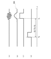
- FIG. 2 is a longitudinal side view of the transducer array in the phased array sensor.
- FIG. 3 is an end view taken along the line III-III in FIG. 2, and illustration of some structural members is omitted.
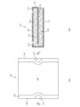
- FIG. 4(a) is a plan view of a piezoelectric element forming a transducer in the transducer array
- FIG. 4(b) is a sectional view taken along the line IV-IV in FIG. 4(a).
- FIG. 5 is a schematic block diagram of a control device and a transmitting unit in the phased array sensor.
- FIG. 5 is a schematic block diagram of a control device and a transmitting unit in the phased array sensor.
- FIG. 6 is a schematic explanatory diagram of the operation when the transducer array emits ultrasonic waves in response to the drive voltage signal supplied from the transmitting side unit.
- FIG. 7 is a schematic block diagram of the receiving side unit and the control device in the phased array sensor.
- FIG. 8 is a schematic explanatory diagram of the operation when the receiving side unit processes a received voltage signal generated by the transducer array in response to reception of ultrasonic waves.
- FIGS. 9(a) and 9(b) show output signals of the adder and detector in the receiving unit, respectively.
- FIG. 9(c) shows the reception timing signal of the received voltage signal generated based on the output signal of the detector, and
- FIG. 9(d) shows the reception timing signal generated based on the signal sent from the control device.
- FIG. 10 is a schematic block diagram of an ultrasonic phased array sensor according to a modification of the first embodiment.
- FIG. 11 is a schematic block diagram of an ultrasonic phased array sensor according to Embodiment 2 of the present invention.
- FIG. 12 is a schematic block diagram of an ultrasonic phased array sensor according to Embodiment 3 of the present invention.
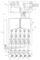
- FIG. 1 shows a schematic block diagram of a phased array sensor 1 according to this embodiment.
- the phased array sensor 1 includes: - The first to nth (n is an integer of 2 or more) non-resonant aerial ultrasonic transducers 110 (first to fifth transducers 110-1 to 110-5 in FIG. 1) are arranged at predetermined intervals.
- a transducer array 100 - a transmission side unit 200 capable of supplying a drive voltage signal to each of the first to n-th transducers 110; - a receiving side unit 300 that processes a received voltage signal generated by each of the first to nth transducers 110 in response to reception of ultrasonic waves; - a switching unit 400 capable of switching between an ultrasonic transmitting operating state and an ultrasonic receiving operating state of the transducer array 100; - A control device 500 that controls the sending unit 200, the receiving unit 300, and the switching unit 400; - A detection device 600 that detects the position of an obstacle based on information regarding the driving voltage signal from the control device 500 and information regarding the received voltage signal from the receiving unit 300 is provided.
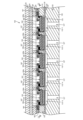
- FIG. 2 shows a longitudinal side view of the transducer array.
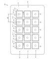
- FIG. 3 shows an end view of the transducer array taken along line III-III in FIG. 2. Note that in FIG. 3, some of the constituent members of the transducer array are omitted for ease of understanding.
- the transducer array 100 has three transducer rows 105-1 to 105-3. -1 to 105-3, five first to fifth transducers 110 are arranged in series at predetermined intervals. Note that in FIG. 1, one row of five transducers 110 is illustrated.
- the transducer 110 is of a non-resonant type that effectively generates ultrasonic waves using a drive voltage having a frequency lower than the frequency of the lowest-order resonance mode of the transducer 110.
- the transducer array 100 includes, as main components, a rigid support plate 120 having a first surface 121 on one side in the thickness direction and a second surface 122 on the other side in the thickness direction; a flexible resin film 130 having a first surface 131 on one side in the thickness direction and a second surface 132 on the other side in the thickness direction, the second surface 132 being fixed to the first surface 121 of the support plate 120; first to nth (five in the figure) piezoelectric elements 140 fixed to the first surface 131 of the flexible resin film 130, the first to nth piezoelectric elements 140 and the flexible resin Corresponding portions of the membrane 130 form the first to nth transducers 110.
- the support plate 120 has the same number of piezoelectric elements 140 (in this embodiment, 3 rows x 5 pieces) opened on the first surface 121 of the support plate 120.
- recesses 125 the first end of which is opened at the bottom surface of the plurality of recesses 125, and the second end of the other end is opened into the second surface 122 of the support plate 120.
- the same number of waveguides 127 as the recesses 125 are provided.
- the waveguide 127 has a cylindrical shape with an opening width smaller than that of the recess 125 and the same opening width throughout the thickness direction.
- the support plate 120 can be made of various rigid members, and can be made of a metal such as stainless steel, or preferably a ceramic material such as SiC or Al2O3, which has a lower density and higher Young's modulus than metal. can.
- the support plate 120 integrally includes a portion where the plurality of recesses 125 are formed and a portion where the plurality of waveguides 127 are formed.
- the support plate 120 is made of a single plate, it is also possible to make the support plate 120 a laminated structure.
- first plate in which the plurality of recesses 125 are formed
- second plate that is separate from the first plate and has a large thickness. It is also possible to form the support body 120 by fixing the second plate body in which the plurality of waveguides 127 are formed in a laminated state in the thickness direction.
- the flexible resin film 130 is fixed to the first surface 121 of the support plate 120 so as to cover the plurality of recesses 125.
- the flexible resin film 130 is made of an insulating resin such as polyimide and has a thickness of 20 ⁇ m to 100 ⁇ m, for example.
- the flexible resin film 130 is fixed to the support plate 120 using various methods such as adhesive or thermocompression bonding.
- the piezoelectric element 140 is formed of the flexible resin so that its central region overlaps with the corresponding recess 125 and its peripheral region overlaps with the first surface 121 of the support plate 120. It is fixed to the first surface 131 of the membrane 130.
- FIG. 4(a) shows a plan view of the piezoelectric element 140. Further, FIG. 4(b) shows a cross-sectional view taken along the line IV-IV in FIG. 4(a).
- the piezoelectric element 140 includes a piezoelectric element body 142 and a pair of first and second electrodes, and is configured to expand and contract when a voltage is applied between the first and second electrodes.
- the piezoelectric element 140 is of a laminated type. Compared to a single-layer piezoelectric element, a laminated piezoelectric element can increase the electric field strength when the same voltage is applied, and can increase the expansion/contraction displacement per applied voltage.
- the piezoelectric element 140 includes a piezoelectric element main body 142 formed of a piezoelectric material such as lead zirconate titanate (PZT), a first piezoelectric portion 142a on the upper side of the piezoelectric element main body 142 in the thickness direction, An inner electrode 144 partitioning the second piezoelectric portion 142b on the lower side, an upper electrode 146 fixed to a part of the upper surface of the first piezoelectric portion 142a, and a lower electrode fixed to the lower surface of the second piezoelectric portion 142b.
- PZT lead zirconate titanate
- the electrode connecting member 145 has one end electrically connected to the lower electrode 147 and the other end insulated from the upper electrode 146 and the inner electrode 34 and accessible on the upper surface of the first piezoelectric portion 32a. It has a lower electrode connecting member 148 forming a lower electrode terminal 147T.
- the outer electrode formed by the upper surface electrode 146 and the lower surface electrode 147 acts as one of the first and second electrodes
- the inner electrode 144 acts as the other of the first and second electrodes.
- the first and second piezoelectric portions 142a and 142b have the same polarization direction in the thickness direction, so that a predetermined voltage is applied between the outer electrode and the inner electrode 144.
- a predetermined voltage is applied between the outer electrode and the inner electrode 144.
- electric fields are applied to the first and second piezoelectric parts 142a and 142b in opposite directions with respect to each other.
- the upper surface electrode 146 and the lower surface electrode 147 are insulated from each other, so when creating the piezoelectric element 140, a voltage is applied between the upper surface electrode 146 and the lower surface electrode 147. By doing so, the polarization directions of the first and second piezoelectric parts 142a and 142b can be made the same.
- the piezoelectric element 140 and the flexible resin film 130 supporting the piezoelectric element 140 generate ultrasonic waves in response to the application of a driving voltage signal, and receive ultrasonic waves. It acts as a transducer 110 that generates a received voltage signal in response.
- the transducer 110 is configured such that the frequency of the lowest order resonance mode of flexural vibration is higher than the frequency (drive frequency) of the voltage signal applied to the piezoelectric element 140.
- a plurality of transducers 110 formed by the plurality of piezoelectric elements 140 are required. It is necessary to precisely control the phase of the sound waves emitted from the
- the piezoelectric elements are expanded and contracted against the rigidity of the rigid support plate, thereby It is necessary to flexibly vibrate the vibrating body formed by the piezoelectric element and the rigid support plate with a predetermined amplitude to ensure the magnitude of the generated sound pressure.
- the frequency response of the flexural vibration of the transducer formed by the piezoelectric element to the voltage applied to the piezoelectric element has a phase that changes significantly near the resonant frequency of the transducer.
- the ultrasonic transducer array 100 has a plurality of recesses 125 opened in the first surface 121 and a first end portion having an opening width smaller than the opening width of the recesses 125.
- the rigid support plate 120 is provided with a plurality of waveguides 127 that are opened at the bottom of the recess 125 and whose second ends are opened at the second surface 122;
- the flexible resin film 130 is fixed to the first surface 121 of the plate 120 so that the central region overlaps the corresponding recess 125 and the peripheral region overlaps the first surface 121 of the support plate 120 in plan view. and the plurality of piezoelectric elements 140 fixed to the first surface 131 of the flexible resin film 130.
- the resonant frequency of the flexural vibration of the transducer 110 formed by the piezoelectric element 140 is set to be higher than the driving frequency of the voltage signal applied to the piezoelectric element 140, the A sufficient vibration amplitude of the transducer 110 can be ensured.
- the resonant frequency of the transducer 110 is higher than the drive frequency of the piezoelectric element 140, even if there is "variation" in the resonant frequency among the plurality of transducers 110, the plurality of transducers 110 There is no significant difference in the phase of the frequency response of the flexural vibration. Therefore, the phase of the sound waves generated by the plurality of transducers 110 can be precisely controlled.
- the frequency of the ultrasonic waves emitted by the transducer 110 formed by the piezoelectric element 140 must be set to a low frequency of about 30 to 50 kHz. There is a need to.
- the resonant frequency of the transducer 110 is set to a sufficiently higher resonant frequency (for example, 70 kHz) than the drive frequency (30 to 50 kHz) of the transducer 110, it is better to increase the vertical and horizontal dimensions of the piezoelectric element 140 in plan view. However, the sound pressure of the ultrasonic waves generated by the transducer 110 can be increased.
- the arrangement pitch of the plurality of transducers 110 needs to be set to 1/2 or less of the wavelength ⁇ of the ultrasonic waves emitted by the transducers 110.
- the vertical and horizontal dimensions of the piezoelectric element 140 in plan view are preferably 3.0 mm or more from the viewpoint of ensuring sound pressure, and 4.0 mm or less from the viewpoint of suppressing the generation of grating lobes.
- the piezoelectric element 140 has a square shape in a plan view, but instead, the piezoelectric element 140 has a shape in a plan view such that the maximum value of the vertical and horizontal dimensions in a plan view is 4. It is also possible to have a rectangular shape including a rectangle with a diameter of 30 mm or less, a circular shape with a diameter of 4.0 mm or less, or an elliptical shape with a major axis of 4.0 mm or less.
- the opening width of the recess 125 is such that the frequency of the lowest resonance mode of the flexural vibration of the transducer 110 formed by the piezoelectric element 140 and the flexible resin film 130 is the frequency of the voltage signal applied to the piezoelectric element 140 ( (driving frequency).
- the recess 125 is formed so that the overlapping width of the peripheral edge region of the piezoelectric element 140 and the support plate 120 in plan view is 0.05 mm to 0.1 mm over the entire circumference of the piezoelectric element 140.
- the shape is similar to that of the piezoelectric element 140 in plan view.
- the recess 125 preferably has a square shape in a plan view with a side of 3.8 mm to 3.9 mm
- the recess 125 preferably has a circular shape in a plan view with a diameter of 3.8 mm to 3.9 mm.
- the rigid support plate 120 is provided with the openings 125 at 15 locations (3 ⁇ 5), and the flexible resin film 130 is The 15 piezoelectric elements 140 are arranged so as to overlap each other with the 15 openings 125 in a plan view when sandwiched between them.
- fifteen transducers 110 are provided, it is understood that the present invention is not limited to such a configuration. In order to sharpen the directivity of the radiated sound waves and increase the intensity, it is desirable to arrange more than 3 ⁇ 5 transducers 110.
- the transducer array 100 further includes a lower sealing plate 150 and a wiring assembly 180.
- the lower sealing plate 150 has a plurality of piezoelectric element openings each having a size that surrounds the plurality of piezoelectric elements 140, and in a plan view, the plurality of piezoelectric elements 140 have a plurality of piezoelectric element openings.
- the first surface 131 of the flexible resin film 130 is fixed to the first surface 131 of the flexible resin film 130 by adhesive or thermocompression bonding so as to be located inside the flexible resin film 130 .
- the thickness of the lower sealing plate 150 is greater than the thickness of the piezoelectric element 140, and the lower sealing plate 150 is fixed to the first surface 131 of the flexible resin film 130. , the first surface of the lower sealing plate 150 is further away from the flexible resin film 130 than the upper surface electrode 146, the lower surface electrode terminal 147T, and the inner electrode terminal 144T (see FIG. 4) of the piezoelectric element 140. are spaced apart.
- the lower sealing plate 150 is formed of a rigid member such as metal such as stainless steel, carbon fiber reinforced plastic, or ceramics.
- the lower sealing plate 150 seals the sides of the piezoelectric element group including the plurality of piezoelectric elements 140, and acts as a base to which the wiring assembly 180 is fixed.
- the wiring assembly 180 transmits the drive voltage signal supplied from the transmission side unit 200 via the switching unit 400 to the first to n-th transducers 110, and A signal transmission path is formed for transmitting a received voltage signal generated by the switching unit 400 to the receiving unit 300 via the switching unit 400.
- the wiring assembly 180 includes an insulating base layer 182 fixed to the lower sealing plate 150 with an adhesive or the like, a conductor layer 185 fixed to the base layer 182, and a conductor layer 185 fixed to the base layer 182. It has an insulating cover layer 187 surrounding the layer 185.
- the base layer 182 and the cover layer 187 are made of, for example, an insulating resin such as polyimide.
- the conductor layer 185 is made of, for example, a conductive metal such as Cu.
- the exposed portion of Cu forming the conductor layer 185 may be plated with Ni/Au.
- the conductor layer 185 is connected to the first electrode (outer electrodes 146 and 147 in this embodiment) and the second electrode (inner electrode 144 in this embodiment) of the piezoelectric element 140. It includes a first wiring 185a and a second wiring 185b that are connected to each other.
- the upper surface electrode 146 and the lower surface electrode 147 act as the first electrode, and the inner electrode 144 acts as the second electrode.
- the first wiring 185a is electrically connected to both a part of the upper surface electrode 146 and the lower surface electrode terminal 147T, for example, by a conductive adhesive or solder.
- the second wiring 185b is electrically connected to the inner electrode terminal 144T by, for example, a conductive adhesive or solder.
- the transducer array 100 further includes an upper sealing plate 160 fixed to the upper surface of the lower sealing plate 150 and the wiring assembly 180 via a flexible resin 155.
- the upper sealing plate 160 has openings 162 at positions corresponding to each of the plurality of piezoelectric elements 140.
- the upper sealing plate 160 is formed of, for example, metal such as stainless steel, carbon fiber reinforced plastic, ceramics, etc. with a thickness of 0.1 mm to 0.3 mm.
- the transducer array 100 further includes a sound absorbing material 165 fixed to the upper surface of the upper sealing plate 160 by adhesive or the like so as to cover the plurality of openings 162 of the upper sealing plate 160.
- the sound absorbing material 165 is made of, for example, silicone resin or other foamable resin with a thickness of about 0.3 mm to 1.5 mm.
- the transducer array 100 further includes a reinforcing plate 170 fixed to the upper surface of the sound absorbing material 165 by adhesive or the like.
- the reinforcing plate 170 is made of, for example, metal such as stainless steel, carbon fiber reinforced plastic, ceramics, etc. and has a thickness of about 0.2 mm to 0.5 mm.
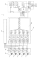
- FIG. 5 shows a schematic block diagram of the control device 500 and the transmitting unit 200.
- FIG. 6 shows a schematic explanatory diagram of the operation when the transducer array 100 emits ultrasonic waves in response to the drive voltage signal supplied from the transmission side unit 200.
- ⁇ is the azimuth angle of the ultrasonic waves emitted from the transducer array 100
- d is the arrangement interval between adjacent transducers
- c is the speed of sound.
- the control device 500 includes a clock signal generation circuit 510 that generates a clock signal with a cycle of, for example, 0.1 ⁇ sec to determine the operation timing of a digital circuit, and a clock signal generated by the clock signal generation circuit 510.
- a time unit setting counter circuit 520 that reduces the frequency of the clock signal to an appropriate time step, for example, a 0.1 msec period for setting the burst wave period; and a burst wave drive that transmits to the first to n-th transducers 110.
- the total time of the burst wave drive voltage signal to be generated is determined.
- an active counter circuit 540 that outputs an active pulse signal with a time width corresponding to the width;
- an azimuth angle control section 550 that outputs an azimuth signal indicating the azimuth angle ⁇ of the ultrasonic waves emitted by the transducer array 100; It has a delay time control section 560 that calculates a delay time ⁇ based on the azimuth signal sent from the angle control section 550 and outputs a delay control signal.
- the transmitting unit 200 includes first to nth signal generating means 220-1 to 220-n for generating drive voltage signals for the first to nth transducers 110, respectively.
- the transmission signal generating device 210 including the first to fifth signal generating means 220-1 to 220-5 in the figure and the driving voltage signals generated by the first to nth signal generating means 220 are It has first to nth transmission side channels 250-1 to 250-n (in the illustration, first to fifth transmission side channels 250-1 to 250-5) that transmit data toward the first to nth transducers 110. are doing.
- the signal generating means 220 includes a frequency divider 222, a delay time counter circuit 224, and a wave number counter circuit 226.
- the frequency divider 222 divides the frequency of the clock signal from the clock signal generation circuit 510 to generate a rectangular burst wave drive voltage signal of a predetermined frequency.
- the delay time counter circuit 224 When activated by the active pulse signal from the active counter circuit 540, the delay time counter circuit 224 controls the frequency divider 222 according to the delay time specified by the delay control signal from the delay time control section 560. A start signal pulse is sent to the frequency divider 222, whereby the frequency divider 222 starts outputting a rectangular burst wave drive voltage signal.
- the wave number counter circuit 226 sends a stop signal pulse to the frequency divider 222 when the wave number of the rectangular burst wave drive voltage signal output from the frequency divider 222 reaches a predetermined wave number.
- the transmitter unit 200 further includes first to n-th channels inserted into the first to n-th transmitter channels 250-1 to 250-n, respectively. It has transmission side filters 260-1 to 260-n (in the illustration, first to fifth transmission side filters 260-1 to 260-5).
- the transmission side filter 260 is configured to remove at least the resonance frequency component of the transducer 110 while allowing the drive frequency component to pass.
- the transmission side filter 260 is a low-pass filter or a band-pass filter configured to remove the resonant frequency component of the transducer while allowing the passage of the driving frequency component, or a filter configured to remove only the resonant frequency component of the transducer 110. It can be a band-stop filter that removes pinpoint signals.
- the bandpass filter is preferably configured to pass only frequency components of ⁇ 10% of the drive frequency.
- the resonant frequency (for example, 70 kHz) of the non-resonant transducer 110 can be effectively passed through while effectively passing the driving frequency (30 to 50 kHz) required to detect an object several meters away. Components can be effectively removed or reduced.
- f is the frequency of the ultrasonic wave
- ⁇ f is the frequency fluctuation due to the Doppler effect
- c is the speed of sound.
- the bandpass filter used as the transmission side filter 260 is configured to pass only the frequency components of ⁇ 1% of the drive frequency, the influence of the Doppler effect can be reduced as much as possible.
- the rectangular burst wave driving voltage signal is converted into a sine wave burst driving voltage signal having the same fundamental frequency (see FIG. 6).
- the transmitter unit 200 includes a power amplifier circuit 270 inserted into the transmitter channel 250 on the downstream side of the transmitter filter 260 in the signal transmission direction. ing.
- the power amplifier circuit 270 includes a buffer circuit 272 and an amplifier circuit 274.
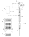
- FIG. 7 shows a schematic block diagram of the receiving unit 300 and the control device 500. Further, FIG. 8 shows a schematic operational explanatory diagram when the receiving unit 300 processes a received voltage signal generated by the transducer array 100 in response to reception of ultrasonic waves.
- the receiving side unit 300 is a first to nth receiving unit capable of receiving received voltage signals generated by the first to nth transducers 110-1 to 110-n, respectively.
- channels 310-1 to 310-n in the illustration, the first to fifth receiving channels 310-1 to 310-5) and the first to nth receiving channels 310-1 to 310-n, respectively.
- the first to nth receiving side filters 320-1 to 320-n in the illustration, the first to fifth receiving side filters 320-1 to 320-5) and the first to nth receiving side channels 320- 1 to 320-n.
- the receiving filter 320 is configured to remove at least the resonant frequency component of the transducer while allowing the drive frequency component to pass.
- the reception side filter 320 may be a low-pass filter or a band-pass filter configured to remove the resonant frequency component of the transducer while allowing the passage of the drive frequency component, or a filter configured to remove only the resonant frequency component of the transducer.
- a band-rejection filter is used that eliminates at a point.
- the bandpass filter is preferably configured to pass only frequency components of ⁇ 10% of the drive frequency.
- the component of the resonant frequency (for example, 70 kHz) of the non-resonant transducer can be transmitted. can be effectively removed or reduced.
- the bandpass filter used as the receiving side filter 320 is preferably configured to pass only frequency components of ⁇ 1% of the driving frequency.
- the receiving side unit 300 includes the first to nth receiving filters 320-1 to 320-n downstream of the first to nth receiving filters 320-1 to 320-n in the signal transmission direction.
- First to n-th low noise amplification circuits 330-1 to 330-n (in the illustration, first to fifth low-noise amplification circuits 330-1 to 330 -5).
- the received signal processing device 350 has first to nth delays that can delay the received voltage signals of the first to nth receiving channels 310-1 to 310-n by corresponding predetermined times. Adding the output signals of the circuits 360-1 to 360-n (in the illustration, the first to fifth delay circuits 360-1 to 360-5) and the first to n-th delay circuits 360-1 to 360-n. It has an adder circuit 370 and a detector 380 that generates a pulse signal having a width corresponding to the duration of the added received voltage signal (time width of the entire signal) generated by the adder circuit 370.
- the delay time of the first to n-th delay circuits 360-1 to 360-n is determined by the delay time of the first to nth delay circuits 360-1 to 360-n. It is set so that only the received voltage signal due to the return ultrasonic wave at the azimuth angle ⁇ reflected from an obstacle existing at the azimuth angle ⁇ at the time of emission and returned to coincide with the time axis.
- the first to n-th delay circuits 360-1 to 360-n each receive signals from the first to n-th receiving channels 310-1 to 310-n sent from the delay time control section 560. Each received voltage signal is delayed by a delay time based on the delay control signal.
- the delay time of the fifth delay circuit 360-5 that delays the received voltage signal from the fifth transducer 110-5 is set to zero, and the received voltage signal from the fourth transducer 110-4 is set to zero.
- the delay time of the fourth delay circuit 360-4 that delays the signal is determined based on the received voltage signal from the fifth transducer 110-5, the arrangement interval d between the adjacent fifth transducer 110-5, and the azimuth angle. It is set to the time ⁇ calculated based on ⁇ and the speed of sound c.
- the delay time of the third delay circuit 360-3 that delays the received voltage signal from the third transducer 110-3 is a time ⁇ with respect to the received voltage signal from the adjacent fourth transducer 110-4. , the time is set to 2 ⁇ based on the received voltage signal from the fifth transducer 110-5.
- the delay time of the second delay circuit 360-2 that delays the received voltage signal from the second transducer 110-2 is the time ⁇ , with respect to the received voltage signal from the adjacent third transducer 110-3. That is, based on the received voltage signal from the fifth transducer 110-5, the time is set to 3 ⁇ , and the delay time of the first delay circuit 360-1 that delays the received voltage signal from the first transducer 110-1 is , is set to a time ⁇ with respect to the received voltage signal from the adjacent second transducer 110-2, that is, a time 4 ⁇ with respect to the received voltage signal from the fifth transducer 110-5.
- the adder circuit 370 receives the received voltage signals of the first to n-th receiving channels 310-1 to 310-n whose time axes are matched by the first to n-th delay circuits 360-1 to 360-n. Add.
- the reflected ultrasonic waves reflected from the obstacle are detected in other directions. It is possible to detect a virtual image based on multiple reflected ultrasound waves that are reflected back from other obstacles in the area.
- the first to n-th transducers 110-1 to 110-n are used both for ultrasonic transmission and ultrasonic reception. It is possible to match only the received voltage signal due to the return ultrasonic wave at the azimuth angle ⁇ , which is emitted towards the angle ⁇ , reflected from an obstacle present at the azimuth angle ⁇ , and returned to the time axis, and detects a virtual image. can be effectively avoided.
- the detector 380 is an envelope detector that extracts a waveform connecting the plus-side vertices of each period in the added received voltage signal generated by the adder circuit 370.
- FIG. 9(a) shows the waveform of the output signal from the adder 370
- FIG. 9(b) shows the waveform of the output signal from the detector 380 (in this embodiment, the envelope detector).
- the received signal processing device 350 includes a signal processing section 375 between the adder 370 and the detector 380 in the signal transmission direction. .
- the signal processing unit 375 may include a variable gain amplifier (not shown), a bandpass filter (not shown), and a logarithmic amplifier (not shown).
- variable gain amplifier increases the amplification as the time difference between the emission timing of the ultrasonic waves from the transducer array 100 due to the drive voltage signal from the transmitting side unit 200 and the reception timing of the returned ultrasonic waves by the transducer array 100 increases. It is configured so that the gain is large.
- variable gain amplifier is provided in consideration of the fact that the more distant the ultrasonic wave returns from an obstacle, the greater the attenuation of the acoustic wave and the smaller the amplitude of the received voltage signal.
- the bandpass filter is configured to pass only the driving frequency component, for example, only the frequency component of 30 kHz to 50 kHz.
- the logarithmic amplifier is configured to have a small gain for signals with small amplitude and a large gain for signals with large amplitude.
- the detection device 600 includes a time difference detection section 610, a direction detection section 620, and a position detection section 630.
- the azimuth detection unit 620 is configured to recognize the azimuth angle ⁇ at which the transducer array 100 emits the ultrasonic waves based on the azimuth information sent from the control device 500.
- the position detection unit 630 identifies the position of the obstacle based on the distance to the obstacle calculated based on the detection result of the time difference detection unit 610 and the azimuth of the obstacle recognized by the azimuth detection unit 620. do.
- the phased array sensor 1 further includes a display device 700 that displays position information of the obstacle identified by the detection device 600. There is.
- the switching unit 400 has first to nth changeover switches 410-1 to 410-n (first to fifth changeover switches 410-1 to 410-5 in the figure). have.
- the first to nth changeover switches 410-1 to 410-n switch the first to nth transducers 110-1 to 100-n, respectively, based on the control signal from the control device 500.
- FIG. 5 shows the transmission states of the first to nth changeover switches 410-1 to 410-n
- FIG. 7 shows the reception states of the first to nth changeover switches 410-1 to 410-n.
- the control device 500 causes the first to nth changeover switches 410-1 to 410-n to be in the transmission state to transmit drive voltage signals to the first to nth transducers 110-1 to 110-n. Immediately after the end, the first to n-th changeover switches 410-1 to 410-n are switched to the receiving state.
- the ultrasonic phased array sensor 1 has the following effects. That is, the transducer 110 is of a non-resonant type that can effectively emit ultrasonic waves even when using a burst wave drive voltage signal having a sufficiently lower drive frequency (for example, 40 kHz) than the resonant frequency (for example, 70 kHz). Even if a drive voltage with a drive frequency sufficiently lower than the resonant frequency of the transducer 110 is applied to the transducer 110 to cause the transducer to emit an ultrasonic wave, the burst wave drive voltage signal is a rectangular wave or rectangular wave. In the case of a waveform close to a wave, not only vibrations at the drive frequency but also vibrations at the resonant frequency of the transducer 110 occur.
- a burst wave drive voltage signal having a sufficiently lower drive frequency (for example, 40 kHz) than the resonant frequency (for example, 70 kHz).
- the generated ultrasonic waveform is distorted, and the damped vibration at the resonant frequency of the transducer 110 after the application of the drive voltage signal is also increased and becomes longer.
- the damped vibration at the resonant frequency of the transducer 110 is the vibration caused by the ultrasonic waves reflected back from the transducer 110 from an obstacle after the transducer array 100 is switched from the transmitting operating state to the receiving operating state. This will greatly impair the accuracy of detecting the position of the obstacle.
- the transducer is allowed to pass through the first to n-th transmission side channels 250-1 to 250-n while allowing the drive frequency components to pass through.
- the first to n-th transmitting side filters 260-1 to 260-n that remove the resonance frequency components of 110 are inserted.
- a burst wave driving voltage converted from a rectangular wave to a sine wave is applied to the transducer 110, and resonance vibration of the transducer 110 is effectively prevented or reduced.
- the above-mentioned disadvantages caused by resonance vibration can be effectively prevented or reduced.
- a sinusoidal burst wave drive voltage signal is applied to the transducer 110, but even in this case, the voltage signal is compared to a rectangular burst wave drive voltage signal. Although the vibration is small, resonant vibration may occur in the transducer 110.
- the transducer is allowed to pass through the first to n-th receiving side channels 310-1 to 310-n while allowing the drive frequency components to pass through.
- the first to n-th receiving side filters 320-1 to 320-n that remove the resonance frequency components of 110 are inserted.
- the received voltage signal is amplified by an amplifier circuit
- the resonance of the transducer 110 The adverse effects of saturation of the amplifier due to signals based on damped oscillations at frequencies can be effectively prevented or reduced.
- FIG. 10 shows a schematic block diagram of an ultrasonic phased array sensor 1' including a receiving unit 300' according to a modified example instead of the receiving unit 300.
- the same members as in this embodiment are given the same reference numerals, and the description thereof will be omitted as appropriate.
- the receiving side unit 300' Compared to the receiving side unit 300, the receiving side unit 300' has first to nth delay circuits 360-1 to 360-n (on the upstream side in the signal transmission direction), respectively. It has D converters 390-1 to 390-n.
- the receiving unit 300' is configured to process the delay circuits 360-1 to 360-n and subsequent received voltage signals by digital signal processing.
- the detector 380 is a quadrature detector.
- the ultrasonic phased array sensor 1' equipped with the receiving unit 300' can also obtain the same effects as the ultrasonic phased array sensor 1 according to the present embodiment.
- FIG. 11 shows a schematic block diagram of the phased array sensor 2 according to this embodiment.
- the same members as those in the first embodiment are designated by the same reference numerals, and detailed explanation thereof will be omitted as appropriate.
- the operating states of the first to n-th transducers 110 can be switched between the ultrasonic transmission operating state and the ultrasonic transmitting state by the first to n-th changeover switches 410.
- the device is configured to switch to a sound wave reception operating state.
- the first to nth transducers 110 act only for transmitting ultrasonic waves, and the first to nth transducers 110 are It has a single airborne ultrasound transducer 112 for reception only.
- the phased array sensor 2 differs from the sensor 1 according to the first embodiment in that the switching unit 400 is deleted, the receiving transducer 112 is included, and the receiving side unit 300 is replaced with the receiving transducer 112. It has a receiving side unit 302 at.
- the phased array sensor 2 includes the first to n-th transducers 110-1 to 110-n (in the illustration, the first to fifth transducers 110-1 to 110-n).
- 110-5) is the transducer array 100 used exclusively for ultrasonic transmission, the transmission signal generator 210, and the first to n-th transmission side channels 250-1 to 250-n (in the illustration, the first - fifth transmitting side channels 250-1 to 250-5) and the first to nth transmitting side filters 260-1 to 260-n (in the illustration, the first to fifth transmitting side filters 260-1 to 260- 5), and a single ultrasonic wave transmitter capable of receiving return ultrasonic waves transmitted from the first to n-th transducers 110-1 to 110n acting as transmission-only transducers and reflected back from obstacles to be detected.
- the receiving aerial ultrasonic transducer 112 the receiving channel 310 capable of receiving the receiving voltage signal generated by the receiving transducer 112; and the receiving filter 320 inserted into the receiving channel 310;
- the time difference between the control device 500 and the transmission timing signal based on the drive voltage signal sent from the control device 500 and the reception timing signal based on the reception voltage signal sent from the detector 380 and the transmission timing signal sent from the control device 500.
- the detection device 600 detects the position of an obstacle based on the received azimuth information.
- the receiving transducer 112 may be of a non-resonant type similar to the transducer 110 acting as a transmitting transducer, or alternatively, the receiving transducer 112 may be of a non-resonant type, in which the transmitting signal is generated by the transmitting signal generator 210. It is also possible to use a resonant type that performs resonance vibration depending on the drive frequency of the drive voltage signal.
- the receiving side filter 320 is configured to remove at least a resonant frequency component of the receiving transducer 112 while allowing passage of a driving frequency component. be done.
- the receiving filter 320 is a noise removal filter.
- the received signal processing device 352 includes the signal processing section 375 upstream of the detector 380 in the signal transmission direction.
- the signal processing unit 375 may include a variable gain amplifier (not shown), a bandpass filter (not shown), and a logarithmic amplifier (not shown).
- FIG. 12 shows a schematic block diagram of the phased array sensor 3 according to this embodiment.
- the same members as in the first and second embodiments are designated by the same reference numerals, and detailed explanation thereof will be omitted as appropriate.
- the phased array sensor 3 differs from the phased array sensor 2 according to the second embodiment in that the phased array sensor 3 functions as a transmitting transducer instead of the single receiving transducer 112. It has first to nth receiving transducers 112-1 to 112-n corresponding to the first to nth transducers 110-1 to 110-n, respectively, and the receiving side unit 302 is replaced by the receiving side unit 302. It has a unit 300.
- the phased array sensor 3 includes the first to nth transducers 110-1 to 110-n (in the illustration, the first to nth transducers 110-1 to 110-n) are used exclusively for ultrasonic transmission.
- the transducer array 100 having five transducers 110-1 to 110-5); 1 to 5 transmission side channels 250-1 to 250-5), and the first to nth transmission side filters 260-1 to 260-n (in the illustration, the first to fifth transmission side filters 260-1 to 260-n). 260-5), and a receiving transducer including the first to nth receiving transducers 112-1 to 112-n (in the illustration, the first to fifth receiving transducers 112-1 to 112-5).
- the first to n-th receiving channels 310-1 to 310-n in the illustration, the first to fifth receiving channels 310-1 to 310-5
- the first to n-th receiving channels side filters 320-1 to 320-n in the illustration, the first to fifth receiving side filters 320-1 to 320-5
- the first to nth receiving side channels 310-1 to 310-n in the illustration, the first to fifth receiving side filters 320-1 to 320-5
- the first to n-th delay circuits 360-1 to 360-n (in the illustration, the first to fifth delay circuits 360-1 to 360-5) each capable of delaying a voltage signal by a predetermined time;
- the received signal includes the addition circuit 370 that adds the output signals of the n delay circuits 360-1 to 360-n, and the detector 380 that generates a signal having a width corresponding to the duration of the output signal of the addition circuit 370.
- the detection device 600 detects the position of an obstacle based on the time difference of the reception timing signal based on the reception voltage signal sent from the control device 500 and the azimuth information sent from the control device 500.
- the receiving transducers 112-1 to 112-n can be of non-resonant type, and unlike this, the driving voltage generated by the transmitting signal generator 210 It is also possible to use a resonant type that performs resonant vibration depending on the driving frequency of the signal.
- the receiving filters 320-1 to 320-n allow at least the receiving transducer to pass through while allowing the driving frequency component to pass through. It is configured to remove resonance frequency components of the inducers 112-1 to 112-n.
- the reception side filters 320-1 to 320-n are noise removal filters.
- the phased array sensor 3 according to the present embodiment can more effectively avoid virtual image detection than the phased array sensor 2 according to the second embodiment.
- the phased array sensor 2 since the phased array sensor 2 according to the second embodiment has only the single reception transducer 112, the transmission transducer array 100 emits radiation at the azimuth angle ⁇ , and the radiation is emitted at the azimuth angle ⁇ . It is not possible to detect only the return ultrasonic waves at the azimuth angle ⁇ that are reflected from existing obstacles and returned.
- the reflected ultrasonic wave reflected from the obstacle is reflected by another obstacle existing in another direction.
- the first to n-th transducers 110-1 to 110- act for transmission, similar to the phased array sensor 1 according to the first embodiment. Only the received voltage signal due to the return ultrasonic wave at the azimuth angle ⁇ reflected from an obstacle existing at the azimuth angle ⁇ from which the ultrasonic wave was emitted by the transducer array 100 having n and returned is matched with respect to the time axis. Detection of virtual images can be effectively avoided.
- a receiving unit (not shown) configured to perform digital signal processing is used instead of the receiving unit 300. ).
- Ultrasonic phased array sensor 100 Transducer array 102 Receiving transducer array 110 Transducer 112 Receiving transducer 210 Transmitting signal generator 220 Signal generating means 250 Transmitting side channel 260 Transmitting side filter 310 Receiving side channel 320 Receiving side Filter 330 Low noise amplification circuits 350, 352 Received signal processing device 410 Changeover switch 500 Control device
Abstract
An ultrasonic phased array sensor according to the present invention comprises: a plurality of non-resonant aerial ultrasonic wave transducers; a transmission signal generation device which generates a rectangular burst wave driving voltage signal of a driving frequency that is lower than the resonant frequency of the transducers; a plurality of transmission-side channels which transfer the driving voltage signal from the transmission signal generation device towards the plurality of transducers; a reception signal processing device; a plurality of reception-side channels which transfer reception voltage signals generated by the plurality of transducers towards the reception signal processing device; a plurality of changeover switches which switch electrical connections to the plurality of transmission-side channels and reception-side channels of the plurality of transducers; a control device; a detection device which detects the position of an obstacle; and a plurality of transmission-side filters and reception-side filters which are respectively inserted into the plurality of transmission side channels and reception side channels, wherein the transmission-side filters and reception-side filters are configured to remove at least a resonant frequency component of the transducers while allowing the passage of driving frequency components.
Description
本発明は、超音波トランスデューサーアレイを有するフェイズドアレイセンサーに関する。
The present invention relates to a phased array sensor having an ultrasonic transducer array.
複数の超音波トランスデューサーが並列配置されてなる超音波トランスデューサーアレイを用いて超音波の送受信を行う場合、超音波の発信動作時には、超音波トランスデューサーアレイは信号発生装置に接続される。
When transmitting and receiving ultrasonic waves using an ultrasonic transducer array consisting of a plurality of ultrasonic transducers arranged in parallel, the ultrasonic transducer array is connected to a signal generator during the ultrasonic transmission operation.
この際、前記複数の超音波トランスデューサーには、所定駆動周波数成分を含む駆動電圧が一定の位相差で順次印加され、前記アレイは前記位相差に対応した方位角へ超音波を放射する。
At this time, drive voltages containing predetermined drive frequency components are sequentially applied to the plurality of ultrasonic transducers with a constant phase difference, and the array emits ultrasonic waves in an azimuth corresponding to the phase difference.
一方、超音波の受信動作時には、前記アレイは、障害物に反射して戻ってくる超音波(受信音波)を受信して、受信音波に基づく電圧信号(受信電圧信号)を発生する。
この際、前記アレイは、前記信号発生装置から切り離されて、信号受信装置に接続される。 On the other hand, during an ultrasonic reception operation, the array receives ultrasonic waves (received sound waves) that are reflected back from an obstacle and generates a voltage signal (received voltage signal) based on the received sound waves.
At this time, the array is separated from the signal generator and connected to the signal receiver.
前記信号受信装置は、前記複数の超音波トランスデューサーがそれぞれ発生する受信電圧信号を順次所定時間ごと遅延させて、加算するように構成されている。ここで、受信電圧信号に対する遅延時間は、放射音波の方位角と同じ方位角からの受信音波に基づく受信電圧信号を加算するように設定される。
The signal receiving device is configured to sequentially delay and add received voltage signals generated by the plurality of ultrasonic transducers by a predetermined time interval. Here, the delay time for the received voltage signal is set such that the received voltage signal based on the received sound wave from the same azimuth as the azimuth of the emitted sound wave is added.
従って、前記アレイは、前記複数の超音波トランスデューサーに対する駆動電圧の位相差(及びこれに応じて設定される受信電圧信号の遅延時間)を変更させることで、広範囲に亘って障害物の位置を検出可能なフェイズドアレイセンサーとして利用される。
Therefore, the array can detect the position of an obstacle over a wide range by changing the phase difference of the driving voltages for the plurality of ultrasonic transducers (and the delay time of the received voltage signal set accordingly). Used as a phased array sensor for detection.
しかしながら、従来のフェイズドアレイセンサーは、以下の問題を有している。
However, conventional phased array sensors have the following problems.
即ち、前記超音波トランスデューサーに印加する駆動電圧としては、通常、制御容易なデジタル回路によって生成される、所定駆動周波数成分を含む矩形波のバースト波電圧信号が用いられる。
That is, as the drive voltage applied to the ultrasonic transducer, a rectangular burst wave voltage signal containing a predetermined drive frequency component, which is generated by an easily controllable digital circuit, is usually used.
前記アレイにおいては、超音波の発信動作時に、前記超音波トランスデューサーに十分に大きな振幅量の振動を行なわせる為に、前記超音波トランスデューサーを共振振動させることが一般的である。
In the array, the ultrasonic transducer is generally vibrated resonantly in order to cause the ultrasonic transducer to vibrate with a sufficiently large amplitude during the ultrasonic transmission operation.
具体的には、前記超音波トランスデューサーには、当該超音波トランスデューサーの共振周波数を主成分とする駆動電圧信号、好ましくは、制御容易なデジタル回路を用いて発生される矩形波のバースト波駆動電圧信号が印加され、これにより、前記超音波トランスデューサーを共振させて、超音波を放射させる。
Specifically, the ultrasonic transducer is driven by a drive voltage signal whose main component is the resonance frequency of the ultrasonic transducer, preferably a rectangular burst wave drive generated using an easily controllable digital circuit. A voltage signal is applied which causes the ultrasound transducer to resonate and emit ultrasound waves.
この場合、駆動電圧信号の印加時には前記超音波トランスデューサーから共振周波数の音波が放射されることになるが、前記超音波トランスデューサーは、駆動電圧信号(矩形波のバースト波電圧信号)の印加が終了した後の暫くの期間においては、共振周波数での減衰振動を行なうことになる。
In this case, when a drive voltage signal is applied, a sound wave at a resonant frequency is emitted from the ultrasonic transducer; After the end of the vibration, damped vibration at the resonant frequency will occur for a while.
従って、近距離に障害物が位置している場合においては、前記超音波トランスデューサーが、減衰振動している間に、障害物に反射して戻ってくる超音波を受信することになり、受信音波によって生じる振動と減衰振動とが重合される事態が生じ得る。
Therefore, when an obstacle is located in a short distance, the ultrasonic transducer will receive the ultrasonic waves reflected from the obstacle and returned while vibrating attenuated. A situation may arise where the vibrations caused by the sound waves and the damped vibrations are superimposed.
前記信号受信装置に備えられる増幅器のゲインは、受信音圧信号の波形が歪まない範囲で可及的に高く設定することが好ましいが、通常、受信音波による振動よりも、共振周波数での減衰振動の方がはるかに大きい為、前記増幅器の増幅ゲインを高く設定すると、前記増幅器の動作飽和を招き、受信電圧信号の波形を維持しながら増幅することができなくなる。
The gain of the amplifier included in the signal receiving device is preferably set as high as possible within a range that does not distort the waveform of the received sound pressure signal; is much larger, so if the amplification gain of the amplifier is set high, the operation of the amplifier will become saturated, making it impossible to amplify the received voltage signal while maintaining its waveform.
また、送信用トランスデューサアレイと受信用トランスデューサアレイとが別になっているタイプのフェイズドアレイセンサーも存在する(下記特許文献1)。このタイプのフェイズドアレイセンサーでは、送信動作後の減衰振動に起因する、前述のような受信電圧信号の増幅が困難になるという問題は生じないが、送信用及び/又は受信用トランスデューサーアレイにおけるトランスデューサの減衰振動が長く続くと、障害物検知の距離分解能が低下することになる。
There is also a type of phased array sensor in which the transmitting transducer array and the receiving transducer array are separate (see Patent Document 1 below). This type of phased array sensor does not suffer from the aforementioned difficulty in amplifying the received voltage signal due to damped oscillations after the transmitting operation, but the transducer in the transmitting and/or receiving transducer array If the damped oscillation continues for a long time, the distance resolution of obstacle detection will decrease.
本願出願人は、前述のような共振型超音波トランスデューサーアレイとは異なるタイプの非共振型超音波トランスデューサーアレイに関する発明を出願し、特許権を取得している(下記特許文献1参照)。
The applicant has filed an application for an invention relating to a non-resonant ultrasonic transducer array that is different from the above-mentioned resonant ultrasonic transducer array, and has obtained a patent right (see Patent Document 1 below).
前記非共振型超音波トランスデューサーアレイは、超音波トランスデューサーの共振周波数を駆動周波数(例えば、40kHz)よりも高く設定することにより、これをフェイズドアレイとして動作させる際に共振周波数の変動の影響を受けることなく駆動周波数での振動の位相を精密に制御できる点において、有用である。
In the non-resonant ultrasonic transducer array, the resonance frequency of the ultrasonic transducer is set higher than the drive frequency (for example, 40 kHz), thereby eliminating the influence of fluctuations in the resonance frequency when operating it as a phased array. This is useful in that it is possible to precisely control the phase of vibration at the drive frequency without being affected.
本願発明者は、この非共振型超音波トランスデューサーアレイに関し鋭意研究を行った結果、下記の新規な課題を見つけ出した。
The inventor of the present application has conducted extensive research on this non-resonant ultrasonic transducer array, and as a result, has discovered the following new problem.
前記非共振型超音波トランスデューサーアレイの超音波トランスデューサーに、共振周波数よりも低い駆動周波数の矩形波のバースト波駆動電圧信号を印加した場合、前記超音波トランスデューサーに駆動周波数よりも高い共振周波数成分を含む信号が印加されることになる。
When a rectangular burst wave driving voltage signal having a driving frequency lower than the resonant frequency is applied to the ultrasonic transducer of the non-resonant ultrasonic transducer array, the resonant frequency higher than the driving frequency is applied to the ultrasonic transducer. A signal containing the component will be applied.
即ち、前記超音波トランスデューサーは、駆動周波数の振動だけでなく、共振周波数の振動も励起されることになり、超音波トランスデューサーから放射される超音波の振動波形が、駆動周波数の振動波形に対して歪む事態が生じ得る。
さらに、駆動電圧信号の印加終了後に、超音波トランスデューサーの共振周波数での減衰振動に起因する問題も生じ得る。 That is, the ultrasonic transducer is excited not only by vibrations at the driving frequency but also by vibrations at the resonant frequency, so that the vibration waveform of the ultrasonic waves emitted from the ultrasonic transducer becomes the vibration waveform at the driving frequency. Distortion may occur.
Furthermore, problems may also arise due to damped vibrations at the resonant frequency of the ultrasound transducer after the application of the drive voltage signal has ended.
なお、下記特許文献2には、複数の超音波トランスデューサーを有する超音波トランスデューサーアレイと、前記超音波トランスデューサーアレイに駆動電圧信号を供給する信号発生装置と、前記超音波トランスデューサーアレイから受信電圧信号を受ける信号受信装置とを備え、前記信号受信装置にはフィルタ回路が設けられているフェイズドアレイセンサーが開示されている。
Note that Patent Document 2 below describes an ultrasonic transducer array having a plurality of ultrasonic transducers, a signal generating device that supplies a driving voltage signal to the ultrasonic transducer array, and a signal generating device that supplies a driving voltage signal to the ultrasonic transducer array. A phased array sensor is disclosed that includes a signal receiving device that receives a voltage signal, and the signal receiving device is provided with a filter circuit.
しかしながら、前記特許文献2の前記フィルタ回路はノイズ等を除去するものであり、前記特許文献2には、超音波トランスデューサーにおける共振周波数での減衰振動に起因する問題については何ら記載されていない。
However, the filter circuit of Patent Document 2 removes noise, etc., and Patent Document 2 does not describe any problems caused by damped vibration at the resonant frequency in the ultrasonic transducer.
本発明は、斯かる従来技術に鑑みなされたものであり、非共振型超音波トランスデューサーアレイを有するフェイズドアレイセンサーであって、超音波トランスデューサーの共振周波数での減衰振動の影響を防止乃至は低減しつつ、超音波の送受信を行うことができるフェイズドアレイセンサーの提供を目的とする。
The present invention has been made in view of the prior art, and is a phased array sensor having a non-resonant ultrasonic transducer array, which prevents the influence of damped vibration at the resonant frequency of the ultrasonic transducer. The purpose of the present invention is to provide a phased array sensor that can transmit and receive ultrasonic waves while reducing ultrasonic waves.
前記目的を達成するために、本発明の第1態様は、複数の非共振型空中超音波トランスデューサーが所定間隔で配列されてなるトランスデューサーアレイと、前記複数のトランスデューサーのそれぞれに対応した複数の信号発生手段であって、前記トランスデューサーの共振周波数よりも低い所定駆動周波数の矩形波のバースト波駆動電圧信号を前記複数のトランスデューサーのそれぞれに対応した遅延時間で発生可能な複数の信号発生手段を有する送信信号発生装置と、前記複数の信号発生手段にそれぞれ接続された複数の送信側チャンネルと、前記複数の送信側チャンネルにそれぞれ介挿された複数の送信側フィルタと、前記複数のトランスデューサーが発生する受信電圧信号をそれぞれ受信可能な複数の受信側チャンネルと、前記複数の受信側チャンネルにそれぞれ介挿された複数の受信側フィルタと、前記複数の受信側チャンネルの受信電圧信号をそれぞれ所定時間遅延可能な複数の遅延回路、前記複数の遅延回路の出力信号を加算する加算回路及び前記加算回路の出力信号の継続時間に対応する幅を有する信号を生成する検波器を含む受信信号処理装置と、前記送信信号発生装置及び前記受信信号処理装置の制御を司る制御装置と、前記制御装置から送られてくる駆動電圧信号に基づく送信タイミング信号及び前記検波器から送られてくる受信電圧信号に基づく受信タイミング信号の時間差並びに前記制御装置から送られてくる方位角情報に基づき、障害物の位置を検出する検知装置と、前記制御装置からの制御信号に基づき、前記複数のトランスデューサーの送信作動状態及び受信作動状態の切替を行う複数の切替スイッチとを備え、前記複数の送信側フィルタ及び前記複数の受信側フィルタは、駆動周波数成分の通過を許容しつつ少なくとも前記トランスデューサーの共振周波数成分を除去するように構成されている超音波フェイズドアレイセンサーを提供する。
In order to achieve the above object, a first aspect of the present invention provides a transducer array in which a plurality of non-resonant aerial ultrasonic transducers are arranged at predetermined intervals, and a plurality of non-resonant aerial ultrasonic transducers corresponding to each of the plurality of transducers. a plurality of signal generation means capable of generating a rectangular burst wave drive voltage signal having a predetermined drive frequency lower than the resonant frequency of the transducer with a delay time corresponding to each of the plurality of transducers; a plurality of transmission side channels respectively connected to the plurality of signal generation means, a plurality of transmission side filters respectively inserted in the plurality of transmission side channels, and the plurality of transformers. a plurality of receiving side channels each capable of receiving received voltage signals generated by the reducer; a plurality of receiving side filters respectively inserted in the plurality of receiving side channels; and a plurality of receiving side filters each capable of receiving received voltage signals of the plurality of receiving side channels. Received signal processing that includes a plurality of delay circuits capable of delaying by a predetermined time, an adder circuit that adds output signals of the plurality of delay circuits, and a detector that generates a signal having a width corresponding to the duration of the output signal of the adder circuit. a control device that controls the transmission signal generation device and the reception signal processing device; a transmission timing signal based on a drive voltage signal sent from the control device; and a reception voltage signal sent from the detector. a detection device that detects the position of an obstacle based on a time difference between reception timing signals based on the azimuth angle information sent from the control device; and a detection device that detects the position of an obstacle based on the time difference between reception timing signals based on and a plurality of changeover switches for switching between an operating state and a reception operating state, and the plurality of transmitter-side filters and the plurality of receiver-side filters allow passage of a drive frequency component and at least a resonant frequency component of the transducer. An ultrasonic phased array sensor configured to remove.
本発明の第1態様に係る超音波フェイズドアレイセンサーによれば、超音波トランスデューサーの共振周波数での減衰振動の影響を防止乃至は低減しつつ、超音波の送受信を行うことができる。
According to the ultrasonic phased array sensor according to the first aspect of the present invention, it is possible to transmit and receive ultrasonic waves while preventing or reducing the influence of damped vibrations at the resonant frequency of the ultrasonic transducer.
第1形態においては、前記送信側フィルタ及び/又は前記受信側フィルタは、前記トランスデューサーの共振周波数成分を除去し且つ駆動周波数成分を通過させるバンドパスフィルタとされる。
In the first form, the transmitter-side filter and/or the receiver-side filter are bandpass filters that remove resonance frequency components of the transducer and pass drive frequency components.
好ましくは、前記バンドパスフィルタは駆動周波数の±10%の周波数成分のみ、より好ましくは、駆動周波数の±1%の周波数成分のみを通過させるように構成される。
第2形態においては、前記送信側フィルタ及び/又は前記受信側フィルタは、前記トランスデューサーの共振周波数成分を除去し且つ駆動周波数成分を通過させるローパスフィルタ又は帯域阻止フィルタとされる。 Preferably, the bandpass filter is configured to pass only frequency components of ±10% of the drive frequency, more preferably only frequency components of ±1% of the drive frequency.
In a second embodiment, the transmitting side filter and/or the receiving side filter are a low pass filter or a band rejection filter that removes a resonance frequency component of the transducer and passes a driving frequency component.
前記種々の構成に係る超音波フェイズドアレイセンサーは、さらに、前記複数の受信側フィルタより信号伝達方向下流側において前記複数の受信側チャンネルにそれぞれ介挿された複数の低雑音増幅回路を有し得る。
The ultrasonic phased array sensor according to the various configurations may further include a plurality of low-noise amplification circuits respectively inserted in the plurality of reception-side channels on the downstream side of the plurality of reception-side filters in the signal transmission direction. .
本発明の第2態様は、複数の送信用非共振型空中超音波トランスデューサーが所定間隔で配列されてなる送信用トランスデューサーアレイと、前記複数の送信用トランスデューサーのそれぞれに対応した複数の信号発生手段であって、前記送信用トランスデューサーの共振周波数よりも低い所定駆動周波数の矩形波のバースト波駆動電圧信号を前記複数の送信用トランスデューサーのそれぞれに対応した遅延時間で発生可能な複数の信号発生手段を有する送信信号発生装置と、前記複数の信号発生手段にそれぞれ接続された複数の送信側チャンネルと、前記複数の送信側チャンネルにそれぞれ介挿された複数の送信側フィルタと、前記複数の送信用トランスデューサーから送信され、検知すべき障害物に反射して戻ってきた戻り超音波を受信可能な受信用空中超音波トランスデューサーと、前記受信用トランスデューサーが発生する受信電圧信号を受信可能な受信側チャンネルと、前記受信側チャンネルに挿された受信側フィルタと、前記受信側チャンネルの出力信号の継続時間に対応する幅を有する信号を生成する検波器を含む受信信号処理装置と、前記送信信号発生装置及び前記受信信号処理装置の制御を司る制御装置と、前記制御装置から送られてくる駆動電圧信号に基づく送信タイミング信号及び前記検波器から送られてくる受信電圧信号に基づく受信タイミング信号の時間差並びに前記制御装置から送られてくる方位角情報に基づき、障害物の位置を検出する検知装置とを備え、前記複数の送信側フィルタは、駆動周波数成分の通過を許容しつつ少なくとも前記送信用トランスデューサーの共振周波数成分を除去するように構成されている超音波フェイズドアレイセンサーを提供する。
A second aspect of the present invention provides a transmitting transducer array in which a plurality of non-resonant aerial ultrasound transducers for transmitting are arranged at predetermined intervals, and a plurality of signals corresponding to each of the plurality of transmitting transducers. A plurality of generating means capable of generating a rectangular burst wave drive voltage signal having a predetermined drive frequency lower than the resonant frequency of the transmitting transducer with a delay time corresponding to each of the plurality of transmitting transducers. a transmission signal generation device having a signal generation means; a plurality of transmission side channels respectively connected to the plurality of signal generation means; a plurality of transmission side filters respectively inserted in the plurality of transmission side channels; a receiving aerial ultrasonic transducer capable of receiving return ultrasonic waves transmitted from the transmitting transducer and returned after being reflected by an obstacle to be detected; and receiving a receiving voltage signal generated by the receiving transducer. a received signal processing device including a possible receiving channel, a receiving filter inserted in the receiving channel, and a detector that generates a signal having a width corresponding to a duration of an output signal of the receiving channel; a control device that controls the transmission signal generation device and the reception signal processing device; a transmission timing signal based on a drive voltage signal sent from the control device; and reception based on a reception voltage signal sent from the detector. and a detection device that detects the position of an obstacle based on the time difference between the timing signals and the azimuth information sent from the control device, and the plurality of transmission-side filters allow at least a drive frequency component to pass through. An ultrasonic phased array sensor configured to remove a resonant frequency component of the transmitting transducer is provided.
本発明の第3態様は、複数の送信用非共振型空中超音波トランスデューサーが所定間隔で配列されてなる送信用トランスデューサーアレイと、前記複数の送信用トランスデューサーのそれぞれに対応した複数の信号発生手段であって、前記送信用トランスデューサーの共振周波数よりも低い所定駆動周波数の矩形波のバースト波駆動電圧信号を前記複数の送信用トランスデューサーのそれぞれに対応した遅延時間で発生可能な複数の信号発生手段を有する送信信号発生装置と、前記複数の信号発生手段にそれぞれ接続された複数の送信側チャンネルと、前記複数の送信側チャンネルにそれぞれ介挿された複数の送信側フィルタと、前記複数の送信用トランスデューサーにそれぞれ対応した複数の受信用空中超音波トランスデューサーを含む受信用トランスデューサーアレイと、前記複数の受信トランスデューサーが発生する受信電圧信号をそれぞれ受信可能な複数の受信側チャンネルと、前記複数の受信側チャンネルにそれぞれ介挿された複数の受信側フィルタと、前記複数の受信側チャンネルの受信電圧信号をそれぞれ所定時間遅延可能な複数の遅延回路、前記複数の遅延回路の出力信号を加算する加算回路及び前記加算回路の出力信号の継続時間に対応する幅を有する信号を生成する検波器を含む受信信号処理装置と、前記送信信号発生装置及び前記受信信号処理装置の制御を司る制御装置と、前記制御装置から送られてくる駆動電圧信号に基づく送信タイミング信号及び前記検波器から送られてくる受信電圧信号に基づく受信タイミング信号の時間差並びに前記制御装置から送られてくる方位角情報に基づき、障害物の位置を検出する検知装置とを備え、前記複数の送信側フィルタは、駆動周波数成分の通過を許容しつつ少なくとも前記送信用トランスデューサーの共振周波数成分を除去するように構成されている超音波フェイズドアレイセンサーを提供する。
A third aspect of the present invention provides a transmitting transducer array in which a plurality of non-resonant aerial ultrasound transducers for transmitting are arranged at predetermined intervals, and a plurality of signals corresponding to each of the plurality of transmitting transducers. A plurality of generating means capable of generating a rectangular burst wave drive voltage signal having a predetermined drive frequency lower than the resonant frequency of the transmitting transducer with a delay time corresponding to each of the plurality of transmitting transducers. a transmission signal generation device having a signal generation means; a plurality of transmission side channels respectively connected to the plurality of signal generation means; a plurality of transmission side filters respectively inserted in the plurality of transmission side channels; a receiving transducer array including a plurality of receiving airborne ultrasonic transducers respectively corresponding to the transmitting transducers; and a plurality of receiving side channels each capable of receiving receiving voltage signals generated by the plurality of receiving transducers. , a plurality of reception side filters respectively inserted in the plurality of reception side channels, a plurality of delay circuits each capable of delaying received voltage signals of the plurality of reception side channels by a predetermined time, and output signals of the plurality of delay circuits. a received signal processing device including an adder circuit that adds up and a detector that generates a signal having a width corresponding to the duration of the output signal of the adder circuit; and a received signal processing device that controls the transmitted signal generation device and the received signal processing device. A time difference between a control device and a transmission timing signal based on a drive voltage signal sent from the control device and a reception timing signal based on a reception voltage signal sent from the detector, and an azimuth sent from the control device. a detection device that detects the position of an obstacle based on the information, and the plurality of transmitting side filters are configured to remove at least a resonant frequency component of the transmitting transducer while allowing passage of a driving frequency component. The company provides ultrasonic phased array sensors.
前記第2及び第3態様において、前記受信用トランスデューサーは、前記送信信号発生装置によって発生される駆動電圧信号の駆動周波数によって共振振動を行う共振型トランスデューサーとされ得る。
In the second and third aspects, the reception transducer may be a resonant transducer that performs resonant vibration based on the drive frequency of the drive voltage signal generated by the transmission signal generator.
これに代えて、前記受信用トランスデューサーは、前記送信信号発生装置によって発生される駆動電圧信号の駆動周波数よりも高い共振周波数を有する非共振型トランスデューサーとされ得る。
Alternatively, the receiving transducer may be a non-resonant transducer having a resonant frequency higher than the driving frequency of the driving voltage signal generated by the transmitting signal generating device.
前記受信用トランスデューサーが共振型トランスデューサーとされる場合には、前記受信側フィルタは、駆動周波数成分の通過を許容しつつ少なくとも前記受信用トランスデューサーの共振周波数成分を除去するように構成される。
When the reception transducer is a resonant transducer, the reception filter is configured to remove at least a resonance frequency component of the reception transducer while allowing passage of a drive frequency component. .
実施の形態1
以下、本発明に係るフェイズドアレイセンサーの一実施の形態について、添付図面を参照しつつ説明する。
図1に、本実施の形態に係るフェイズドアレイセンサー1の模式ブロック図を示す。Embodiment 1
DESCRIPTION OF THE PREFERRED EMBODIMENTS An embodiment of a phased array sensor according to the present invention will be described below with reference to the accompanying drawings.
FIG. 1 shows a schematic block diagram of a phasedarray sensor 1 according to this embodiment.
以下、本発明に係るフェイズドアレイセンサーの一実施の形態について、添付図面を参照しつつ説明する。
図1に、本実施の形態に係るフェイズドアレイセンサー1の模式ブロック図を示す。
DESCRIPTION OF THE PREFERRED EMBODIMENTS An embodiment of a phased array sensor according to the present invention will be described below with reference to the accompanying drawings.
FIG. 1 shows a schematic block diagram of a phased
図1に示すように、前記フェイズドアレイセンサー1は、
・第1~第n(nは2以上の整数)の非共振型空中超音波トランスデューサー110(図1においては第1~第5トランスデューサー110-1~110-5)が所定間隔で配列されてなるトランスデューサーアレイ100と、
・前記第1~第nトランスデューサー110のそれぞれに対して駆動電圧信号を供給可能な送信側ユニット200と、
・前記第1~第nトランスデューサー110のそれぞれが超音波の受信に応じて発生する受信電圧信号を処理する受信側ユニット300と、
・前記トランスデューサーアレイ100の超音波発信作動状態及び超音波受信作動状態を切替可能な切替ユニット400と、
・前記送信側ユニット200、前記受信側ユニット300及び前記切替ユニット400の制御を司る制御装置500と、
・前記制御装置500からの駆動電圧信号に関する情報及び前記受信側ユニット300からの受信電圧信号に関する情報に基づき障害物の位置を検知する検知装置600と
を備えている。 As shown in FIG. 1, the phasedarray sensor 1 includes:
- The first to nth (n is an integer of 2 or more) non-resonant aerial ultrasonic transducers 110 (first to fifth transducers 110-1 to 110-5 in FIG. 1) are arranged at predetermined intervals. atransducer array 100,
- atransmission side unit 200 capable of supplying a drive voltage signal to each of the first to n-th transducers 110;
- areceiving side unit 300 that processes a received voltage signal generated by each of the first to nth transducers 110 in response to reception of ultrasonic waves;
- aswitching unit 400 capable of switching between an ultrasonic transmitting operating state and an ultrasonic receiving operating state of the transducer array 100;
- Acontrol device 500 that controls the sending unit 200, the receiving unit 300, and the switching unit 400;
- Adetection device 600 that detects the position of an obstacle based on information regarding the driving voltage signal from the control device 500 and information regarding the received voltage signal from the receiving unit 300 is provided.
・第1~第n(nは2以上の整数)の非共振型空中超音波トランスデューサー110(図1においては第1~第5トランスデューサー110-1~110-5)が所定間隔で配列されてなるトランスデューサーアレイ100と、
・前記第1~第nトランスデューサー110のそれぞれに対して駆動電圧信号を供給可能な送信側ユニット200と、
・前記第1~第nトランスデューサー110のそれぞれが超音波の受信に応じて発生する受信電圧信号を処理する受信側ユニット300と、
・前記トランスデューサーアレイ100の超音波発信作動状態及び超音波受信作動状態を切替可能な切替ユニット400と、
・前記送信側ユニット200、前記受信側ユニット300及び前記切替ユニット400の制御を司る制御装置500と、
・前記制御装置500からの駆動電圧信号に関する情報及び前記受信側ユニット300からの受信電圧信号に関する情報に基づき障害物の位置を検知する検知装置600と
を備えている。 As shown in FIG. 1, the phased
- The first to nth (n is an integer of 2 or more) non-resonant aerial ultrasonic transducers 110 (first to fifth transducers 110-1 to 110-5 in FIG. 1) are arranged at predetermined intervals. a
- a
- a
- a
- A
- A
まず、前記トランスデューサーアレイ100について説明する。
図2に、前記トランスデューサーアレイの縦断側面図を示す。
また、図3に、図2におけるIII-III線に沿った前記トランスデューサーアレイの端面図を示す。なお、図3においては、理解容易化の為に前記トランスデューサーアレイの構成部材の一部の表示を省略している。 First, thetransducer array 100 will be explained.
FIG. 2 shows a longitudinal side view of the transducer array.
Further, FIG. 3 shows an end view of the transducer array taken along line III-III in FIG. 2. Note that in FIG. 3, some of the constituent members of the transducer array are omitted for ease of understanding.
図2に、前記トランスデューサーアレイの縦断側面図を示す。
また、図3に、図2におけるIII-III線に沿った前記トランスデューサーアレイの端面図を示す。なお、図3においては、理解容易化の為に前記トランスデューサーアレイの構成部材の一部の表示を省略している。 First, the
FIG. 2 shows a longitudinal side view of the transducer array.
Further, FIG. 3 shows an end view of the transducer array taken along line III-III in FIG. 2. Note that in FIG. 3, some of the constituent members of the transducer array are omitted for ease of understanding.
図2及び図3に示すように、本実施の形態においては、前記トランスデューサーアレイ100は、3列のトランスデューサー列105-1~105-3を有しており、3列のトランスデューサー列105-1~105-3のそれぞれにおいて第1~第5の5つのトランスデューサー110が所定間隔で直列配列されている。
なお、図1においては、1列分の5つのトランスデューサー110が図示されている。 As shown in FIGS. 2 and 3, in this embodiment, thetransducer array 100 has three transducer rows 105-1 to 105-3. -1 to 105-3, five first to fifth transducers 110 are arranged in series at predetermined intervals.
Note that in FIG. 1, one row of fivetransducers 110 is illustrated.
なお、図1においては、1列分の5つのトランスデューサー110が図示されている。 As shown in FIGS. 2 and 3, in this embodiment, the
Note that in FIG. 1, one row of five
前記トランスデューサー110は、当該トランスデューサー110の最低次の共振モードの周波数よりも低い周波数の駆動電圧によって、有効に超音波を発生する非共振型とされている。
The transducer 110 is of a non-resonant type that effectively generates ultrasonic waves using a drive voltage having a frequency lower than the frequency of the lowest-order resonance mode of the transducer 110.
詳しくは、図2に示すように、前記トランスデューサーアレイ100は、主要構成部材として、厚み方向一方側の第1面121及び厚み方向他方側の第2面122を有する剛性の支持板120と、厚み方向一方側の第1面131及び厚み方向他方側の第2面132を有し、第2面132が前記支持板120の第1面121に固着された可撓性樹脂膜130と、前記可撓性樹脂膜130の第1面131に固着された第1~第n(図示においては5つ)の圧電素子140とを備え、前記第1~第n圧電素子140及び前記可撓性樹脂膜130の対応する部分が第1~第nのトランスデューサー110を形成している。
Specifically, as shown in FIG. 2, the transducer array 100 includes, as main components, a rigid support plate 120 having a first surface 121 on one side in the thickness direction and a second surface 122 on the other side in the thickness direction; a flexible resin film 130 having a first surface 131 on one side in the thickness direction and a second surface 132 on the other side in the thickness direction, the second surface 132 being fixed to the first surface 121 of the support plate 120; first to nth (five in the figure) piezoelectric elements 140 fixed to the first surface 131 of the flexible resin film 130, the first to nth piezoelectric elements 140 and the flexible resin Corresponding portions of the membrane 130 form the first to nth transducers 110.
図2及び図3に示すように、前記支持板120には、当該支持板120の第1面121に開口された、前記圧電素子140と同数(本実施の形態においては3列×5個の15個)の凹部125と、一端側の第1端部が前記複数の凹部125の底面にそれぞれ開口され且つ他端側の第2端部が当該支持板120の第2面122に開口された、前記凹部125と同数(本実施の形態においては3×5の15個)の導波路127とが設けられている。
As shown in FIGS. 2 and 3, the support plate 120 has the same number of piezoelectric elements 140 (in this embodiment, 3 rows x 5 pieces) opened on the first surface 121 of the support plate 120. (15) recesses 125, the first end of which is opened at the bottom surface of the plurality of recesses 125, and the second end of the other end is opened into the second surface 122 of the support plate 120. , and the same number of waveguides 127 as the recesses 125 (in this embodiment, 15 (3×5)) are provided.
本実施の形態においては、前記導波路127は、開口幅が前記凹部125の開口幅よりも小で且つ厚み方向全域に亘って同一開口幅の筒状とされている。
In the present embodiment, the waveguide 127 has a cylindrical shape with an opening width smaller than that of the recess 125 and the same opening width throughout the thickness direction.
前記支持板120は、剛性を有する種々の部材によって形成することができ、ステンレス等の金属、好ましくは、金属よりも密度が小さく且つヤング率の高いSiC、Al2O3等のセラミックス材料によって形成することができる。
The support plate 120 can be made of various rigid members, and can be made of a metal such as stainless steel, or preferably a ceramic material such as SiC or Al2O3, which has a lower density and higher Young's modulus than metal. can.
図2及び図3に示すように、本実施の形態においては、前記支持板120は、前記複数の凹部125が形成された部分及び前記複数の導波路127が形成された部分を一体的に備えた単一板とされているが、前記支持板120を積層構造体とすることも可能である。
As shown in FIGS. 2 and 3, in this embodiment, the support plate 120 integrally includes a portion where the plurality of recesses 125 are formed and a portion where the plurality of waveguides 127 are formed. Although the support plate 120 is made of a single plate, it is also possible to make the support plate 120 a laminated structure.
即ち、前記複数の凹部125が形成された第1板体(図示せず)と、前記第1板体とは別体で且つ板厚が大とされた第2板体(図示せず)であって、前記複数の導波路127が形成された第2板体とを厚み方向に積層状態で固着させて、前記支持体120を形成することも可能である。
That is, a first plate (not shown) in which the plurality of recesses 125 are formed, and a second plate (not shown) that is separate from the first plate and has a large thickness. It is also possible to form the support body 120 by fixing the second plate body in which the plurality of waveguides 127 are formed in a laminated state in the thickness direction.
前記可撓性樹脂膜130は、前記複数の凹部125を覆うように前記支持板120の第1面121に固着されている。
The flexible resin film 130 is fixed to the first surface 121 of the support plate 120 so as to cover the plurality of recesses 125.
前記可撓性樹脂膜130は、例えば、厚さ20μm~100μmのポリイミド等の絶縁性樹脂によって形成される。
前記可撓性樹脂膜130は、接着剤又は熱圧着等の種々の方法によって前記支持板120に固着される。 Theflexible resin film 130 is made of an insulating resin such as polyimide and has a thickness of 20 μm to 100 μm, for example.
Theflexible resin film 130 is fixed to the support plate 120 using various methods such as adhesive or thermocompression bonding.
前記可撓性樹脂膜130は、接着剤又は熱圧着等の種々の方法によって前記支持板120に固着される。 The
The
図3に示すように、前記圧電素子140は、平面視において中央領域が対応する凹部125と重合し且つ周縁領域が前記支持板120の第1面121と重合するように、前記可撓性樹脂膜130の第1面131に固着されている。
As shown in FIG. 3, the piezoelectric element 140 is formed of the flexible resin so that its central region overlaps with the corresponding recess 125 and its peripheral region overlaps with the first surface 121 of the support plate 120. It is fixed to the first surface 131 of the membrane 130.
図4(a)に、前記圧電素子140の平面図を示す。
また、図4(b)に、図4(a)におけるIV-IV線に沿った断面図を示す。
前記圧電素子140は、圧電素子本体142と、一対の第1及び第2電極とを有し、前記第1及び第2電極の間に電圧が印可されると伸縮するように構成されている。 FIG. 4(a) shows a plan view of thepiezoelectric element 140.
Further, FIG. 4(b) shows a cross-sectional view taken along the line IV-IV in FIG. 4(a).
Thepiezoelectric element 140 includes a piezoelectric element body 142 and a pair of first and second electrodes, and is configured to expand and contract when a voltage is applied between the first and second electrodes.
また、図4(b)に、図4(a)におけるIV-IV線に沿った断面図を示す。
前記圧電素子140は、圧電素子本体142と、一対の第1及び第2電極とを有し、前記第1及び第2電極の間に電圧が印可されると伸縮するように構成されている。 FIG. 4(a) shows a plan view of the
Further, FIG. 4(b) shows a cross-sectional view taken along the line IV-IV in FIG. 4(a).
The
本実施の形態においては、前記圧電素子140は積層型とされている。
積層型圧電素子は、単層型圧電素子に比して、同一電圧印可時に電界強度を高めることができ、印可電圧当たりの伸縮変位を大きくすることができる。 In this embodiment, thepiezoelectric element 140 is of a laminated type.
Compared to a single-layer piezoelectric element, a laminated piezoelectric element can increase the electric field strength when the same voltage is applied, and can increase the expansion/contraction displacement per applied voltage.
積層型圧電素子は、単層型圧電素子に比して、同一電圧印可時に電界強度を高めることができ、印可電圧当たりの伸縮変位を大きくすることができる。 In this embodiment, the
Compared to a single-layer piezoelectric element, a laminated piezoelectric element can increase the electric field strength when the same voltage is applied, and can increase the expansion/contraction displacement per applied voltage.
詳しくは、前記圧電素子140は、チタン酸ジルコン酸鉛(PZT)等の圧電材によって形成される前記圧電素子本体142と、前記圧電素子本体142を厚み方向に関し上方側の第1圧電部位142a及び下方側の第2圧電部位142bに区画する内側電極144と、前記第1圧電部位142aの上面の一部に固着された上面電極146と、前記第2圧電部位142bの下面に固着された下面電極147と、一端部が前記内側電極144に電気的に接続され且つ他端部が前記上面電極146とは絶縁状態で前記第1圧電部位142aの上面においてアクセス可能な内側電極端子144Tを形成する内側電極用接続部材145と、一端部が前記下面電極147に電気的に接続され且つ他端部が前記上面電極146及び前記内側電極34とは絶縁状態で前記第1圧電部位32aの上面においてアクセス可能な下面電極端子147Tを形成する下面電極用接続部材148とを有している。
Specifically, the piezoelectric element 140 includes a piezoelectric element main body 142 formed of a piezoelectric material such as lead zirconate titanate (PZT), a first piezoelectric portion 142a on the upper side of the piezoelectric element main body 142 in the thickness direction, An inner electrode 144 partitioning the second piezoelectric portion 142b on the lower side, an upper electrode 146 fixed to a part of the upper surface of the first piezoelectric portion 142a, and a lower electrode fixed to the lower surface of the second piezoelectric portion 142b. 147, and an inner electrode terminal 144T having one end electrically connected to the inner electrode 144 and the other end being insulated from the upper surface electrode 146 and accessible on the upper surface of the first piezoelectric portion 142a. The electrode connecting member 145 has one end electrically connected to the lower electrode 147 and the other end insulated from the upper electrode 146 and the inner electrode 34 and accessible on the upper surface of the first piezoelectric portion 32a. It has a lower electrode connecting member 148 forming a lower electrode terminal 147T.
この場合、前記上面電極146及び前記下面電極147によって形成される外側電極が第1及び第2電極の一方として作用し、前記内側電極144が第1及び第2電極の他方として作用する。
In this case, the outer electrode formed by the upper surface electrode 146 and the lower surface electrode 147 acts as one of the first and second electrodes, and the inner electrode 144 acts as the other of the first and second electrodes.
前記圧電素子140においては、前記第1及び第2圧電部位142a、142bは、分極方向が厚み方向に関し同一とされており、これにより、前記外側電極及び前記内側電極144の間に所定の電圧を所定周波数で印可することによって、前記第1及び第2圧電部位142a、142bには互いに対して逆方向の電界が加わるようになっている。
In the piezoelectric element 140, the first and second piezoelectric portions 142a and 142b have the same polarization direction in the thickness direction, so that a predetermined voltage is applied between the outer electrode and the inner electrode 144. By applying a predetermined frequency, electric fields are applied to the first and second piezoelectric parts 142a and 142b in opposite directions with respect to each other.
前述の通り、前記上面電極146及び前記下面電極147は互いに対して絶縁されており、従って、前記圧電素子140を作成する際には、前記上面電極146及び前記下面電極147の間に電圧を印可することによって、前記第1及び第2圧電部位142a、142bの分極方向を同一とすることができる。
As described above, the upper surface electrode 146 and the lower surface electrode 147 are insulated from each other, so when creating the piezoelectric element 140, a voltage is applied between the upper surface electrode 146 and the lower surface electrode 147. By doing so, the polarization directions of the first and second piezoelectric parts 142a and 142b can be made the same.
前述の通り、前記超音波トランスデューサーアレイ100においては、前記圧電素子140及びこれを支持する前記可撓性樹脂膜130が駆動電圧信号の印加に応じて超音波を発生し且つ超音波の受信に応じて受信電圧信号を発生するトランスデューサー110として作用する。そして、このトランスデューサー110は、たわみ振動の最低次の共振モードの周波数が前記圧電素子140への印加電圧信号の周波数(駆動周波数)よりも大となるように構成されている。
As described above, in the ultrasonic transducer array 100, the piezoelectric element 140 and the flexible resin film 130 supporting the piezoelectric element 140 generate ultrasonic waves in response to the application of a driving voltage signal, and receive ultrasonic waves. It acts as a transducer 110 that generates a received voltage signal in response. The transducer 110 is configured such that the frequency of the lowest order resonance mode of flexural vibration is higher than the frequency (drive frequency) of the voltage signal applied to the piezoelectric element 140.
即ち、トランスデューサー110を形成する複数の圧電素子140が並列配置されているフェイズドアレイによって、数メートル先の物体を検知する為には、前記複数の圧電素子140によって形成される複数のトランスデューサー110から放射される音波の位相を精密に制御する必要がある。
That is, in order to detect an object several meters away using a phased array in which a plurality of piezoelectric elements 140 forming a transducer 110 are arranged in parallel, a plurality of transducers 110 formed by the plurality of piezoelectric elements 140 are required. It is necessary to precisely control the phase of the sound waves emitted from the
例えば、ステンレス等の剛性の支持板に直接的に複数の圧電素子が並列配置されている構成のフェイズドアレイにおいては、前記剛性支持板の剛性に抗して前記圧電素子を伸縮させ、それによって前記圧電素子及び前記剛性支持板によって形成される振動体を所定の振幅でたわみ振動させて、発生音圧の大きさを確保する必要がある。
For example, in a phased array in which a plurality of piezoelectric elements are directly arranged in parallel on a rigid support plate such as stainless steel, the piezoelectric elements are expanded and contracted against the rigidity of the rigid support plate, thereby It is necessary to flexibly vibrate the vibrating body formed by the piezoelectric element and the rigid support plate with a predetermined amplitude to ensure the magnitude of the generated sound pressure.
その為には、前記圧電素子への印可電圧の周波数(駆動周波数)を、当該圧電素子によって形成されるトランスデューサーのたわみ振動の共振周波数の近傍に設定する必要がある。
For this purpose, it is necessary to set the frequency (drive frequency) of the voltage applied to the piezoelectric element near the resonance frequency of the flexural vibration of the transducer formed by the piezoelectric element.
しかしながら、前記圧電素子への印可電圧に対する、当該圧電素子によって形成されるトランスデューサーのたわみ振動の周波数応答は、当該トランスデューサーの共振周波数近傍において位相が大きく変化する。
However, the frequency response of the flexural vibration of the transducer formed by the piezoelectric element to the voltage applied to the piezoelectric element has a phase that changes significantly near the resonant frequency of the transducer.
従って、フェイズドアレイセンサーとして機能させるべく、前記複数のトランスデューサーが発生する音波の位相を精密に制御する為には、前記複数のトランスデューサー間における共振周波数に関する「ばらつき」を極限まで抑制する必要があるが、これは非常に難しい。
Therefore, in order to precisely control the phase of the sound waves generated by the plurality of transducers in order to function as a phased array sensor, it is necessary to suppress "dispersion" in the resonance frequency among the plurality of transducers to the utmost. Yes, but this is extremely difficult.
この点に関し、前記超音波トランスデューサーアレイ100は、前述の通り、第1面121に開口された複数の凹部125及び前記凹部125の開口幅よりも開口幅が小とされた第1端部が前記凹部125の底面に開口され且つ第2端部が第2面122に開口された複数の導波路127が設けられた前記剛性の支持板120と、前記複数の凹部125を覆うように前記支持板120の第1面121に固着された可撓性樹脂膜130と、平面視において中央領域が対応する凹部125と重合し且つ周縁領域が前記支持板120の第1面121と重合するように前記可撓性樹脂膜130の第1面131に固着された前記複数の圧電素子140とを有している。
In this regard, as described above, the ultrasonic transducer array 100 has a plurality of recesses 125 opened in the first surface 121 and a first end portion having an opening width smaller than the opening width of the recesses 125. The rigid support plate 120 is provided with a plurality of waveguides 127 that are opened at the bottom of the recess 125 and whose second ends are opened at the second surface 122; The flexible resin film 130 is fixed to the first surface 121 of the plate 120 so that the central region overlaps the corresponding recess 125 and the peripheral region overlaps the first surface 121 of the support plate 120 in plan view. and the plurality of piezoelectric elements 140 fixed to the first surface 131 of the flexible resin film 130.
斯かる構成によれば、前記圧電素子140によって形成されるトランスデューサー110のたわみ振動の共振周波数が、前記圧電素子140に印加する電圧信号の駆動周波数よりも高くなるように設定しても、前記トランスデューサー110の振動振幅を十分に確保することができる。
According to such a configuration, even if the resonant frequency of the flexural vibration of the transducer 110 formed by the piezoelectric element 140 is set to be higher than the driving frequency of the voltage signal applied to the piezoelectric element 140, the A sufficient vibration amplitude of the transducer 110 can be ensured.
しかも、前記トランスデューサー110の共振周波数が前記圧電素子140の駆動周波数よりも高い場合には、前記複数のトランスデューサー110間において共振周波数の「ばらつき」があったとしても、前記複数のトランスデューサー110のたわみ振動の周波数応答の位相に大きな差異は生じない。
従って、前記複数のトランスデューサー110が発生する音波の位相を精密に制御することができる。 Moreover, if the resonant frequency of thetransducer 110 is higher than the drive frequency of the piezoelectric element 140, even if there is "variation" in the resonant frequency among the plurality of transducers 110, the plurality of transducers 110 There is no significant difference in the phase of the frequency response of the flexural vibration.
Therefore, the phase of the sound waves generated by the plurality oftransducers 110 can be precisely controlled.
従って、前記複数のトランスデューサー110が発生する音波の位相を精密に制御することができる。 Moreover, if the resonant frequency of the
Therefore, the phase of the sound waves generated by the plurality of
詳しくは、前記超音波トランスデューサーアレイ100によって数メートル先の物体を検知する為には、前記圧電素子140によって形成されるトランスデューサー110が放射する超音波の周波数を30~50kHz程度の低周波数とする必要がある。
Specifically, in order to detect an object several meters away using the ultrasonic transducer array 100, the frequency of the ultrasonic waves emitted by the transducer 110 formed by the piezoelectric element 140 must be set to a low frequency of about 30 to 50 kHz. There is a need to.
前記トランスデューサー110の共振周波数を、前記トランスデューサー110の駆動周波数(30~50kHz)よりも十分に高い共振周波数(例えば、70kHz)とした場合、前記圧電素子140の平面視縦横寸法を大きくした方が、前記トランスデューサー110が発生する超音波の音圧を高くすることができる。
When the resonant frequency of the transducer 110 is set to a sufficiently higher resonant frequency (for example, 70 kHz) than the drive frequency (30 to 50 kHz) of the transducer 110, it is better to increase the vertical and horizontal dimensions of the piezoelectric element 140 in plan view. However, the sound pressure of the ultrasonic waves generated by the transducer 110 can be increased.
しかしながら、その一方で、前記トランスデューサーアレイ100におけるように、複数のトランスデューサー110(複数の圧電素子140)が並列配置されてなる場合においては、前記複数のトランスデューサー110から放射される音波においてグレーティングローブの発生を抑制する為に、前記複数のトランスデューサー110(複数の圧電素子140)の配列ピッチを当該トランスデューサー110が放射する超音波の波長λの1/2以下にする必要がある。
However, on the other hand, in a case where a plurality of transducers 110 (a plurality of piezoelectric elements 140) are arranged in parallel as in the transducer array 100, a grating is generated in the sound waves emitted from the plurality of transducers 110. In order to suppress the generation of lobes, the arrangement pitch of the plurality of transducers 110 (the plurality of piezoelectric elements 140) needs to be set to 1/2 or less of the wavelength λ of the ultrasonic waves emitted by the transducers 110.
周波数40kHzの超音波の波長λは8.6mmであるから、前記トランスデューサー110が放射する超音波の周波数を40kHzとしつつ、グレーティングローブの発生を抑制する為に、前記複数のトランスデューサー110(複数の圧電素子140)の配列ピッチd(図3参照)を8.6mm/2=4.3mm以下にする必要がある。
Since the wavelength λ of an ultrasonic wave with a frequency of 40 kHz is 8.6 mm, in order to suppress the generation of grating lobes while setting the frequency of the ultrasonic wave emitted by the transducer 110 to 40 kHz, the plurality of transducers 110 (multiple The arrangement pitch d (see FIG. 3) of the piezoelectric elements 140) needs to be 8.6 mm/2=4.3 mm or less.
従って、好ましくは、前記圧電素子140の平面視縦横寸法は、音圧の確保の観点では3.0mm以上で、且つ、グレーティングローブの発生を抑制する観点では4.0mm以下とされる。
Therefore, the vertical and horizontal dimensions of the piezoelectric element 140 in plan view are preferably 3.0 mm or more from the viewpoint of ensuring sound pressure, and 4.0 mm or less from the viewpoint of suppressing the generation of grating lobes.
なお、本実施の形態においては、前記圧電素子140は、平面視正方形状とされているが、これに代えて、前記圧電素子140の平面視形状を、平面視縦横寸法の最大値が4.30mm以下の長方形を含む矩形状、直径が4.0mm以下の円形状、又は、長径が4.0mm以下の楕円形状とすることも可能である。
In the present embodiment, the piezoelectric element 140 has a square shape in a plan view, but instead, the piezoelectric element 140 has a shape in a plan view such that the maximum value of the vertical and horizontal dimensions in a plan view is 4. It is also possible to have a rectangular shape including a rectangle with a diameter of 30 mm or less, a circular shape with a diameter of 4.0 mm or less, or an elliptical shape with a major axis of 4.0 mm or less.
前記凹部125の開口幅は、前記圧電素子140及び前記可撓性樹脂膜130が形成するトランスデューサー110のたわみ振動の最低次の共振モードの周波数が当該圧電素子140への印加電圧信号の周波数(駆動周波数)よりも大となるように、設定される。
The opening width of the recess 125 is such that the frequency of the lowest resonance mode of the flexural vibration of the transducer 110 formed by the piezoelectric element 140 and the flexible resin film 130 is the frequency of the voltage signal applied to the piezoelectric element 140 ( (driving frequency).
好ましくは、前記凹部125は、前記圧電素子140の周縁領域と前記支持板120との平面視重合幅が前記圧電素子140の全周に亘って0.05mm~0.1mmとなるように、前記圧電素子140の平面視相似形状とされる。
Preferably, the recess 125 is formed so that the overlapping width of the peripheral edge region of the piezoelectric element 140 and the support plate 120 in plan view is 0.05 mm to 0.1 mm over the entire circumference of the piezoelectric element 140. The shape is similar to that of the piezoelectric element 140 in plan view.
即ち、仮に、前記圧電素子140が一辺4.0mmの平面視正方形状とされている場合には、前記凹部125は、好ましくは、一辺3.8mm~3.9mmの平面視正方形状とされ、前記圧電素子140が直径4.0mmの平面視円形状とされている場合には、前記凹部125は、好ましくは、直径3.8mm~3.9mmの平面視円形状とされる。
That is, if the piezoelectric element 140 has a square shape in a plan view with a side of 4.0 mm, the recess 125 preferably has a square shape in a plan view with a side of 3.8 mm to 3.9 mm, When the piezoelectric element 140 has a circular shape in a plan view with a diameter of 4.0 mm, the recess 125 preferably has a circular shape in a plan view with a diameter of 3.8 mm to 3.9 mm.
図2及び図3等に示すように、本実施の形態においては、前記剛性の支持板120には前記開口部125が3×5の15か所において設けられ、前記可撓性樹脂膜130を挟んだ状態で15か所の開口部125とそれぞれ平面視において重合するように15個の圧電素子140が配列されており、これにより、前記15個の圧電素子140がそれぞれ形成する3×5の15個のトランスデューサー110が備えられているが、当然ながら、本発明は斯かる構成に限定されるものではない。
放射音波の指向性を鋭くし、強度を高めるためには 3×5 より多いトランスデューサー110を配列することが望ましい。 As shown in FIGS. 2 and 3, in this embodiment, therigid support plate 120 is provided with the openings 125 at 15 locations (3×5), and the flexible resin film 130 is The 15 piezoelectric elements 140 are arranged so as to overlap each other with the 15 openings 125 in a plan view when sandwiched between them. Although fifteen transducers 110 are provided, it is understood that the present invention is not limited to such a configuration.
In order to sharpen the directivity of the radiated sound waves and increase the intensity, it is desirable to arrange more than 3×5transducers 110.
放射音波の指向性を鋭くし、強度を高めるためには 3×5 より多いトランスデューサー110を配列することが望ましい。 As shown in FIGS. 2 and 3, in this embodiment, the
In order to sharpen the directivity of the radiated sound waves and increase the intensity, it is desirable to arrange more than 3×5
本実施の形態においては、図2に示すように、前記トランスデューサーアレイ100は、さらに、下側封止板150及び配線アッセンブリ180を有している。
In this embodiment, as shown in FIG. 2, the transducer array 100 further includes a lower sealing plate 150 and a wiring assembly 180.
前記下側封止板150は、前記複数の圧電素子140をそれぞれ囲む大きさの複数の圧電素子用開口を有しており、平面視において前記複数の圧電素子140が前記複数の圧電素子用開口内に位置するように前記可撓性樹脂膜130の第1面131に接着剤又は熱圧着等によって固着されている。
The lower sealing plate 150 has a plurality of piezoelectric element openings each having a size that surrounds the plurality of piezoelectric elements 140, and in a plan view, the plurality of piezoelectric elements 140 have a plurality of piezoelectric element openings. The first surface 131 of the flexible resin film 130 is fixed to the first surface 131 of the flexible resin film 130 by adhesive or thermocompression bonding so as to be located inside the flexible resin film 130 .
図2に示すように、前記下側封止板150の厚さは、前記圧電素子140の厚さよりも大とされており、前記可撓性樹脂膜130の第1面131に固着された状態において前記下側封止板150の第1面が、前記圧電素子140における前記上面電極146、前記下面電極端子147T及び前記内側電極端子144T(図4参照)よりも前記可撓性樹脂膜130から離間されている。
As shown in FIG. 2, the thickness of the lower sealing plate 150 is greater than the thickness of the piezoelectric element 140, and the lower sealing plate 150 is fixed to the first surface 131 of the flexible resin film 130. , the first surface of the lower sealing plate 150 is further away from the flexible resin film 130 than the upper surface electrode 146, the lower surface electrode terminal 147T, and the inner electrode terminal 144T (see FIG. 4) of the piezoelectric element 140. are spaced apart.
前記下側封止板150は、ステンレス等の金属や炭素繊維強化プラスチック及びセラミックス等の剛性部材によって形成される。
前記下側封止板150は、前記複数の圧電素子140を含む圧電素子群の側方を封止するとともに、前記配線アッセンブリ180が固着される基台として作用する。 Thelower sealing plate 150 is formed of a rigid member such as metal such as stainless steel, carbon fiber reinforced plastic, or ceramics.
Thelower sealing plate 150 seals the sides of the piezoelectric element group including the plurality of piezoelectric elements 140, and acts as a base to which the wiring assembly 180 is fixed.
前記下側封止板150は、前記複数の圧電素子140を含む圧電素子群の側方を封止するとともに、前記配線アッセンブリ180が固着される基台として作用する。 The
The
前記配線アッセンブリ180は、前記送信側ユニット200から前記切替ユニット400を介して供給される駆動電圧信号を前記第1~第nトランスデューサー110に伝達し、且つ、前記第1~第nトランスデューサー110が発生する受信電圧信号を前記切替ユニット400を介して前記受信側ユニット300へ伝達する為の信号伝達経路を形成する。
The wiring assembly 180 transmits the drive voltage signal supplied from the transmission side unit 200 via the switching unit 400 to the first to n-th transducers 110, and A signal transmission path is formed for transmitting a received voltage signal generated by the switching unit 400 to the receiving unit 300 via the switching unit 400.
図2に示すように、前記配線アッセンブリ180は、前記下側封止板150に接着剤等によって固着される絶縁性ベース層182と、前記ベース層182に固着された導体層185と、前記導体層185を囲繞する絶縁性のカバー層187とを有している。
As shown in FIG. 2, the wiring assembly 180 includes an insulating base layer 182 fixed to the lower sealing plate 150 with an adhesive or the like, a conductor layer 185 fixed to the base layer 182, and a conductor layer 185 fixed to the base layer 182. It has an insulating cover layer 187 surrounding the layer 185.
前記ベース層182及び前記カバー層187は、例えば、ポリイミド等の絶縁性樹脂によって形成される。
前記導体層185は、例えば、Cu等の導電性金属によって形成される。
好ましくは、前記導体層185を形成するCuの露出部分にNi/Auメッキを施すことができる。 Thebase layer 182 and the cover layer 187 are made of, for example, an insulating resin such as polyimide.
The conductor layer 185 is made of, for example, a conductive metal such as Cu.
Preferably, the exposed portion of Cu forming the conductor layer 185 may be plated with Ni/Au.
前記導体層185は、例えば、Cu等の導電性金属によって形成される。
好ましくは、前記導体層185を形成するCuの露出部分にNi/Auメッキを施すことができる。 The
The conductor layer 185 is made of, for example, a conductive metal such as Cu.
Preferably, the exposed portion of Cu forming the conductor layer 185 may be plated with Ni/Au.
本実施の形態においては、前記導体層185は、前記圧電素子140の第1電極(本実施の形態においては外側電極146、147)及び第2電極(本実施の形態においては内側電極144)にそれぞれ接続される第1配線185a及び第2配線185bを含んでいる。
In this embodiment, the conductor layer 185 is connected to the first electrode ( outer electrodes 146 and 147 in this embodiment) and the second electrode (inner electrode 144 in this embodiment) of the piezoelectric element 140. It includes a first wiring 185a and a second wiring 185b that are connected to each other.
本実施の形態においては、前述の通り、前記上面電極146及び前記下面電極147が前記第1電極として作用し且つ前記内側電極144が前記第2電極として作用している。
In this embodiment, as described above, the upper surface electrode 146 and the lower surface electrode 147 act as the first electrode, and the inner electrode 144 acts as the second electrode.
従って、前記第1配線185aが前記上面電極146の一部及び前記下面電極端子147Tの双方に、例えば、導電性接着剤又ははんだによって電気的に接続されている。
Therefore, the first wiring 185a is electrically connected to both a part of the upper surface electrode 146 and the lower surface electrode terminal 147T, for example, by a conductive adhesive or solder.
そして、前記第2配線185bが前記内側電極端子144Tに、例えば、導電性接着剤又ははんだによって電気的に接続されている。
The second wiring 185b is electrically connected to the inner electrode terminal 144T by, for example, a conductive adhesive or solder.
前記トランスデューサーアレイ100は、さらに、前記下側封止板150及び前記配線アッセンブリ180の上面に柔軟性樹脂155を介して固着された上側封止板160を有している。
前記上側封止板160は、前記複数の圧電素子140のそれぞれに対応した位置に開口部162を有している。 Thetransducer array 100 further includes an upper sealing plate 160 fixed to the upper surface of the lower sealing plate 150 and the wiring assembly 180 via a flexible resin 155.
Theupper sealing plate 160 has openings 162 at positions corresponding to each of the plurality of piezoelectric elements 140.
前記上側封止板160は、前記複数の圧電素子140のそれぞれに対応した位置に開口部162を有している。 The
The
前記上側封止板160を備えることにより、前記トランスデューサー110の振動動作への影響を可及的に防止しつつ、前記配線アッセンブリ180の支持安定化を図ることができる。
By providing the upper sealing plate 160, it is possible to stabilize the support of the wiring assembly 180 while preventing the influence on the vibration operation of the transducer 110 as much as possible.
前記上側封止板160は、例えば、厚さ0.1mm~0.3mmのステンレス等の金属や炭素繊維強化プラスチック及びセラミックス等によって形成される。
The upper sealing plate 160 is formed of, for example, metal such as stainless steel, carbon fiber reinforced plastic, ceramics, etc. with a thickness of 0.1 mm to 0.3 mm.
前記トランスデューサーアレイ100は、さらに、前記上側封止板160の複数の開口部162を覆うように前記上側封止板160の上面に接着等によって固着された吸音材165を備えている。
The transducer array 100 further includes a sound absorbing material 165 fixed to the upper surface of the upper sealing plate 160 by adhesive or the like so as to cover the plurality of openings 162 of the upper sealing plate 160.
前記吸音材165は、例えば、厚さ0.3mm~1.5mm程度のシリコーン樹脂又は他の発泡性樹脂によって形成される。
The sound absorbing material 165 is made of, for example, silicone resin or other foamable resin with a thickness of about 0.3 mm to 1.5 mm.
前記吸音材165を備えることにより、前記トランスデューサー110によって生成される超音波が放射されるべき側(図2において下側)とは反対側へ放射されることを有効に抑制することができる。
By providing the sound absorbing material 165, it is possible to effectively suppress the ultrasonic waves generated by the transducer 110 from being radiated to the side opposite to the side to be radiated (lower side in FIG. 2).
前記トランスデューサーアレイ100は、さらに、前記吸音材165の上面に接着等によって固着された補強板170を備えている。
The transducer array 100 further includes a reinforcing plate 170 fixed to the upper surface of the sound absorbing material 165 by adhesive or the like.
前記補強板170は、例えば、厚さ0.2mm~0.5mm程度のステンレス等の金属や炭素繊維強化プラスチック及びセラミックス等によって形成される。
The reinforcing plate 170 is made of, for example, metal such as stainless steel, carbon fiber reinforced plastic, ceramics, etc. and has a thickness of about 0.2 mm to 0.5 mm.
前記補強板170を備えることにより、外力が前記基板120及び前記圧電素子140に影響を与えることを可及的に防止することができる。
By providing the reinforcing plate 170, it is possible to prevent external forces from affecting the substrate 120 and the piezoelectric element 140 as much as possible.
次に、前記制御装置500及び前記送信側ユニット200について説明する。
図5に、前記制御装置500及び前記送信側ユニット200の模式ブロック図を示す。 Next, thecontrol device 500 and the sending unit 200 will be explained.
FIG. 5 shows a schematic block diagram of thecontrol device 500 and the transmitting unit 200.
図5に、前記制御装置500及び前記送信側ユニット200の模式ブロック図を示す。 Next, the
FIG. 5 shows a schematic block diagram of the
また、図6に、前記送信側ユニット200から供給される駆動電圧信号によって前記トランスデューサーアレイ100が超音波を放射する際の模式動作説明図を示す。
なお、図6中のτは、一のトランスデューサー110(例えば第1トランスデューサー110-1)に印加するバースト波駆動電圧信号と、隣接するトランスデューサー110(例えば第2トランスデューサー110-2)に印加するバースト波駆動電圧信号との遅延時間であり、
τ=d×sinθ/c
によって算出される。
ここで、θは前記トランスデューサーアレイ100から放射される超音波の方位角、dは隣接するトランスデューサーの配列間隔、cは音速である。 Further, FIG. 6 shows a schematic explanatory diagram of the operation when thetransducer array 100 emits ultrasonic waves in response to the drive voltage signal supplied from the transmission side unit 200.
Note that τ in FIG. 6 is the difference between the burst wave drive voltage signal applied to one transducer 110 (for example, the first transducer 110-1) and the adjacent transducer 110 (for example, the second transducer 110-2). It is the delay time with the applied burst wave drive voltage signal,
τ=d×sinθ/c
Calculated by
Here, θ is the azimuth angle of the ultrasonic waves emitted from thetransducer array 100, d is the arrangement interval between adjacent transducers, and c is the speed of sound.
なお、図6中のτは、一のトランスデューサー110(例えば第1トランスデューサー110-1)に印加するバースト波駆動電圧信号と、隣接するトランスデューサー110(例えば第2トランスデューサー110-2)に印加するバースト波駆動電圧信号との遅延時間であり、
τ=d×sinθ/c
によって算出される。
ここで、θは前記トランスデューサーアレイ100から放射される超音波の方位角、dは隣接するトランスデューサーの配列間隔、cは音速である。 Further, FIG. 6 shows a schematic explanatory diagram of the operation when the
Note that τ in FIG. 6 is the difference between the burst wave drive voltage signal applied to one transducer 110 (for example, the first transducer 110-1) and the adjacent transducer 110 (for example, the second transducer 110-2). It is the delay time with the applied burst wave drive voltage signal,
τ=d×sinθ/c
Calculated by
Here, θ is the azimuth angle of the ultrasonic waves emitted from the
図5に示すように、前記制御装置500は、デジタル回路の動作タイミングを決める為の例えば0.1μsec周期のクロック信号を発生するクロック信号発生回路510と、前記クロック信号発生回路510で発生されたクロック信号の周波数を、バースト波周期を設定する為に適切な時間刻み、例えば0.1msec周期に低下させる時間単位設定カウンター回路520と、前記第1~第nトランスデューサー110に送信するバースト波駆動電圧信号の発生タイミングの間隔でパルスを発生するバースト間隔カウンター回路530と、前記時間単位設定カウンター回路520及び前記バースト間隔カウンター回路530からの信号に基づき、発生させるべきバースト波駆動電圧信号の全体時間幅に対応した時間幅のアクティブパルス信号を出力するアクティブカウンター回路540と、前記トランスデューサーアレイ100が放射する超音波の方位角θを示す方位角信号を出力する方位角制御部550と、前記方位角制御部550から送られてくる方位角信号に基づき遅延時間τを算出し、遅延制御信号を出力する遅延時間制御部560とを有している。
As shown in FIG. 5, the control device 500 includes a clock signal generation circuit 510 that generates a clock signal with a cycle of, for example, 0.1 μsec to determine the operation timing of a digital circuit, and a clock signal generated by the clock signal generation circuit 510. a time unit setting counter circuit 520 that reduces the frequency of the clock signal to an appropriate time step, for example, a 0.1 msec period for setting the burst wave period; and a burst wave drive that transmits to the first to n-th transducers 110. Based on the signals from the burst interval counter circuit 530 that generates pulses at intervals of the generation timing of the voltage signal, the time unit setting counter circuit 520, and the burst interval counter circuit 530, the total time of the burst wave drive voltage signal to be generated is determined. an active counter circuit 540 that outputs an active pulse signal with a time width corresponding to the width; an azimuth angle control section 550 that outputs an azimuth signal indicating the azimuth angle θ of the ultrasonic waves emitted by the transducer array 100; It has a delay time control section 560 that calculates a delay time τ based on the azimuth signal sent from the angle control section 550 and outputs a delay control signal.
図1及び図5に示すように、前記送信側ユニット200は、前記第1~第nトランスデューサー110のそれぞれに対する駆動電圧信号を発生する第1~第n信号発生手段220-1~220-n(図示においては第1~第5信号発生手段220-1~220-5)を含む送信信号発生装置210と、前記第1~第n信号発生手段220によって発生された駆動電圧信号をそれぞれ前記第1~第nトランスデューサー110に向けて伝達する第1~第n送信側チャンネル250-1~250-n(図示においては第1~第5送信側チャンネル250-1~250-5)とを有している。
As shown in FIGS. 1 and 5, the transmitting unit 200 includes first to nth signal generating means 220-1 to 220-n for generating drive voltage signals for the first to nth transducers 110, respectively. The transmission signal generating device 210 including the first to fifth signal generating means 220-1 to 220-5 in the figure and the driving voltage signals generated by the first to nth signal generating means 220 are It has first to nth transmission side channels 250-1 to 250-n (in the illustration, first to fifth transmission side channels 250-1 to 250-5) that transmit data toward the first to nth transducers 110. are doing.
図5に示すように、前記信号発生手段220は、分周器222と、遅延時間カウンター回路224と、波数カウンター回路226とを有している。
As shown in FIG. 5, the signal generating means 220 includes a frequency divider 222, a delay time counter circuit 224, and a wave number counter circuit 226.
前記分周器222は、前記クロック信号発生回路510からのクロック信号を分周して、所定周波数の矩形波のバースト波駆動電圧信号を生成する。
The frequency divider 222 divides the frequency of the clock signal from the clock signal generation circuit 510 to generate a rectangular burst wave drive voltage signal of a predetermined frequency.
前記遅延時間カウンター回路224は、前記アクティブカウンター回路540からのアクティブパルス信号によってアクティブとされると、前記遅延時間制御部560からの遅延制御信号によって指定された遅延時間に応じて前記分周器222にスタート信号パルスを送り、これにより、前記分周器222が矩形波のバースト波駆動電圧信号の出力を開始する。
When activated by the active pulse signal from the active counter circuit 540, the delay time counter circuit 224 controls the frequency divider 222 according to the delay time specified by the delay control signal from the delay time control section 560. A start signal pulse is sent to the frequency divider 222, whereby the frequency divider 222 starts outputting a rectangular burst wave drive voltage signal.
前記波数カウンター回路226は、前記分周器222から出力される矩形波のバースト波駆動電圧信号の波数が所定波数に到達すると前記分周器222にストップ信号パルスを送る。
The wave number counter circuit 226 sends a stop signal pulse to the frequency divider 222 when the wave number of the rectangular burst wave drive voltage signal output from the frequency divider 222 reaches a predetermined wave number.
図5に示すように、本実施の形態においては、前記送信側ユニット200は、さらに、前記第1~第n送信側チャンネル250-1~250-nにそれぞれ介挿された第1~第n送信側フィルタ260-1~260-n(図示においては、第1~第5送信側フィルタ260-1~260-5)を有している。
As shown in FIG. 5, in the present embodiment, the transmitter unit 200 further includes first to n-th channels inserted into the first to n-th transmitter channels 250-1 to 250-n, respectively. It has transmission side filters 260-1 to 260-n (in the illustration, first to fifth transmission side filters 260-1 to 260-5).
前記送信側フィルタ260は、駆動周波数成分の通過を許容しつつ少なくとも前記トランスデューサー110の共振周波数成分を除去するように構成されている。
The transmission side filter 260 is configured to remove at least the resonance frequency component of the transducer 110 while allowing the drive frequency component to pass.
前記送信側フィルタ260は、駆動周波数成分の通過を許容しつつ前記トランスデューサーの共振周波数成分を除去するように構成されたローパスフィルタ又はバンドパスフィルタ、若しくは、前記トランスデューサー110の共振周波数成分のみをピンポイントで除去する帯域阻止フィルタとされ得る。
The transmission side filter 260 is a low-pass filter or a band-pass filter configured to remove the resonant frequency component of the transducer while allowing the passage of the driving frequency component, or a filter configured to remove only the resonant frequency component of the transducer 110. It can be a band-stop filter that removes pinpoint signals.
前記送信側フィルタ260がバンドパスフィルタとされた構成においては、好ましくは、前記バンドパスフィルタは、駆動周波数の±10%の周波数成分のみを通過させるように構成される。
In a configuration in which the transmitting side filter 260 is a bandpass filter, the bandpass filter is preferably configured to pass only frequency components of ±10% of the drive frequency.
斯かる構成によれば、数メートル先の物体を検知する為に必要とされる駆動周波数(30~50kHz)を有効に通過させつつ、非共振型トランスデューサー110の共振周波数(例えば、70kHz)の成分を有効に除去乃至は低減することができる。
According to such a configuration, the resonant frequency (for example, 70 kHz) of the non-resonant transducer 110 can be effectively passed through while effectively passing the driving frequency (30 to 50 kHz) required to detect an object several meters away. Components can be effectively removed or reduced.
例えば、本実施の形態に係る超音波フェイズドアレイセンサー1をサービスロボット等の障害物に対する最大相対速度差vが10km/h(=2.78m/sec)程度の装置に装着される場合には、
△f/f=±v/c=±0.00808(=±0.808%)
となる。
ここで、fは超音波の周波数、△fはドップラー効果による周波数変動、及び、cは音速である。 For example, when the ultrasonic phasedarray sensor 1 according to the present embodiment is installed in a device such as a service robot where the maximum relative speed difference v with respect to an obstacle is about 10 km/h (=2.78 m/sec),
△f/f=±v/c=±0.00808 (=±0.808%)
becomes.
Here, f is the frequency of the ultrasonic wave, Δf is the frequency fluctuation due to the Doppler effect, and c is the speed of sound.
△f/f=±v/c=±0.00808(=±0.808%)
となる。
ここで、fは超音波の周波数、△fはドップラー効果による周波数変動、及び、cは音速である。 For example, when the ultrasonic phased
△f/f=±v/c=±0.00808 (=±0.808%)
becomes.
Here, f is the frequency of the ultrasonic wave, Δf is the frequency fluctuation due to the Doppler effect, and c is the speed of sound.
従って、前記送信側フィルタ260として用いられるバンドパスフィルタが駆動周波数の±1%の周波数成分のみを通過させるように構成すれば、ドップラー効果による影響を可及的に低減することができる。
Therefore, if the bandpass filter used as the transmission side filter 260 is configured to pass only the frequency components of ±1% of the drive frequency, the influence of the Doppler effect can be reduced as much as possible.
前記送信側フィルタ260を通過させることによって、矩形波のバースト波駆動電圧信号から、基本周波数は同一の正弦波のバースト波駆動電圧信号(図6参照)に変換される。
これにより、矩形波の場合には存在していた、駆動電圧信号の各周期毎の急激な立ち上がり及び立ち下りの波形が緩やかな波形に変換される。 By passing through thetransmission side filter 260, the rectangular burst wave driving voltage signal is converted into a sine wave burst driving voltage signal having the same fundamental frequency (see FIG. 6).
As a result, the waveform of the drive voltage signal having rapid rises and falls in each cycle, which existed in the case of a rectangular wave, is converted into a gentle waveform.
これにより、矩形波の場合には存在していた、駆動電圧信号の各周期毎の急激な立ち上がり及び立ち下りの波形が緩やかな波形に変換される。 By passing through the
As a result, the waveform of the drive voltage signal having rapid rises and falls in each cycle, which existed in the case of a rectangular wave, is converted into a gentle waveform.
本実施の形態においては、図5に示すように、前記送信側ユニット200は、前記送信側フィルタ260より信号伝達方向下流側において前記送信側チャンネル250に介挿された電力増幅回路270を有している。
前記電力増幅回路270は、バッファ回路272及び増幅回路274を有している。 In this embodiment, as shown in FIG. 5, thetransmitter unit 200 includes a power amplifier circuit 270 inserted into the transmitter channel 250 on the downstream side of the transmitter filter 260 in the signal transmission direction. ing.
Thepower amplifier circuit 270 includes a buffer circuit 272 and an amplifier circuit 274.
前記電力増幅回路270は、バッファ回路272及び増幅回路274を有している。 In this embodiment, as shown in FIG. 5, the
The
次に、前記受信側ユニット300について説明する。
図7に、前記受信側ユニット300及び前記制御装置500の模式ブロック図を示す。
また、図8に、前記トランスデューサーアレイ100が超音波の受信に応じて発生した受信電圧信号を前記受信側ユニット300が処理する際の模式動作説明図を示す。 Next, the receivingunit 300 will be explained.
FIG. 7 shows a schematic block diagram of the receivingunit 300 and the control device 500.
Further, FIG. 8 shows a schematic operational explanatory diagram when the receivingunit 300 processes a received voltage signal generated by the transducer array 100 in response to reception of ultrasonic waves.
図7に、前記受信側ユニット300及び前記制御装置500の模式ブロック図を示す。
また、図8に、前記トランスデューサーアレイ100が超音波の受信に応じて発生した受信電圧信号を前記受信側ユニット300が処理する際の模式動作説明図を示す。 Next, the receiving
FIG. 7 shows a schematic block diagram of the receiving
Further, FIG. 8 shows a schematic operational explanatory diagram when the receiving
図1及び図7に示すように、前記受信側ユニット300は、前記第1~第nトランスデューサー110-1~110-nが発生する受信電圧信号をそれぞれ受信可能な第1~第n受信側チャンネル310-1~310-n(図示においては第1~第5受信側チャンネル310-1~310-5)と、前記第1~第n受信側チャンネル310-1~310-nにそれぞれ介挿された第1~第n受信側フィルタ320-1~320-n(図示においては第1~第5受信側フィルタ320-1~320-5)と、前記第1~第n受信側チャンネル320-1~320-nからの受信電圧信号を処理する受信信号処理装置350とを有している。
As shown in FIGS. 1 and 7, the receiving side unit 300 is a first to nth receiving unit capable of receiving received voltage signals generated by the first to nth transducers 110-1 to 110-n, respectively. channels 310-1 to 310-n (in the illustration, the first to fifth receiving channels 310-1 to 310-5) and the first to nth receiving channels 310-1 to 310-n, respectively. the first to nth receiving side filters 320-1 to 320-n (in the illustration, the first to fifth receiving side filters 320-1 to 320-5) and the first to nth receiving side channels 320- 1 to 320-n.
前記受信側フィルタ320は、駆動周波数成分の通過を許容しつつ少なくとも前記トランスデューサーの共振周波数成分を除去するように構成されている。
The receiving filter 320 is configured to remove at least the resonant frequency component of the transducer while allowing the drive frequency component to pass.
前記受信側フィルタ320として、駆動周波数成分の通過を許容しつつ前記トランスデューサーの共振周波数成分を除去するように構成されたローパスフィルタ又はバンドパスフィルタ、若しくは、前記トランスデューサーの共振周波数成分のみをピンポイントで除去する帯域阻止フィルタが用いられる。
The reception side filter 320 may be a low-pass filter or a band-pass filter configured to remove the resonant frequency component of the transducer while allowing the passage of the drive frequency component, or a filter configured to remove only the resonant frequency component of the transducer. A band-rejection filter is used that eliminates at a point.
前記受信側フィルタ320がバンドパスフィルタとされた構成においては、好ましくは、前記バンドパスフィルタは、駆動周波数の±10%の周波数成分のみを通過させるように構成される。
In a configuration in which the reception side filter 320 is a bandpass filter, the bandpass filter is preferably configured to pass only frequency components of ±10% of the drive frequency.
斯かる構成によれば、数メートル先の物体を検知する為に必要とされる駆動周波数(30~50kHz)を有効に通過させつつ、非共振型トランスデューサーの共振周波数(例えば、70kHz)の成分を有効に除去乃至は低減することができる。
According to such a configuration, while effectively passing the driving frequency (30 to 50 kHz) required to detect an object several meters away, the component of the resonant frequency (for example, 70 kHz) of the non-resonant transducer can be transmitted. can be effectively removed or reduced.
本実施の形態に係る超音波フェイズドアレイセンサー1をサービスロボット等の障害物に対する最大相対速度差vが10km/h(=2.78m/sec)程度の装置に装着される場合には、前記送信側フィルタ260と同様に、前記受信側フィルタ320として用いられるバンドパスフィルタは、好ましくは、駆動周波数の±1%の周波数成分のみを通過させるように構成される。
When the ultrasonic phased array sensor 1 according to the present embodiment is installed in a device such as a service robot where the maximum relative velocity difference v with respect to an obstacle is about 10 km/h (=2.78 m/sec), the above-mentioned transmission Similar to the side filter 260, the bandpass filter used as the receiving side filter 320 is preferably configured to pass only frequency components of ±1% of the driving frequency.
本実施の形態においては、図7に示すように、前記受信側ユニット300は、前記第1~第n受信側フィルタ320-1~320-nより信号伝達方向下流側において前記第1~第n受信側チャンネル310-1~310-nにそれぞれ介挿された第1~第n低雑音増幅回路330-1~330-n(図示においては第1~第5低雑音増幅回路330-1~330-5)を有している。
In this embodiment, as shown in FIG. 7, the receiving side unit 300 includes the first to nth receiving filters 320-1 to 320-n downstream of the first to nth receiving filters 320-1 to 320-n in the signal transmission direction. First to n-th low noise amplification circuits 330-1 to 330-n (in the illustration, first to fifth low-noise amplification circuits 330-1 to 330 -5).
図7に示すように、前記受信信号処理装置350は、前記第1~第n受信側チャンネル310-1~310-nの受信電圧信号をそれぞれ対応する所定時間遅延可能な第1~第n遅延回路360-1~360-n(図示においては第1~第5遅延回路360-1~360-5)と、前記第1~第n遅延回路360-1~360-nの出力信号を加算する加算回路370と、前記加算回路370によって生成された加算受信電圧信号の継続時間(信号全体の時間幅)に対応する幅を有するパルス信号を生成する検波器380とを有している。
As shown in FIG. 7, the received signal processing device 350 has first to nth delays that can delay the received voltage signals of the first to nth receiving channels 310-1 to 310-n by corresponding predetermined times. Adding the output signals of the circuits 360-1 to 360-n (in the illustration, the first to fifth delay circuits 360-1 to 360-5) and the first to n-th delay circuits 360-1 to 360-n. It has an adder circuit 370 and a detector 380 that generates a pulse signal having a width corresponding to the duration of the added received voltage signal (time width of the entire signal) generated by the adder circuit 370.
前記第1~第n遅延回路360-1~360-nの遅延時間は、前記トランスデューサーアレイ100が超音波を受信することによって発生する受信電圧信号のうち、前記トランスデューサーアレイ100が超音波を放射した際の方位角θに存在する障害物に反射して戻ってきた方位角θの戻り超音波による受信電圧信号のみを時間軸に対して一致させるように、設定される。
The delay time of the first to n-th delay circuits 360-1 to 360-n is determined by the delay time of the first to nth delay circuits 360-1 to 360-n. It is set so that only the received voltage signal due to the return ultrasonic wave at the azimuth angle θ reflected from an obstacle existing at the azimuth angle θ at the time of emission and returned to coincide with the time axis.
具体的には、前記第1~第n遅延回路360-1~360-nは、前記遅延時間制御部560から送られてくる前記第1~第n受信側チャンネル310-1~310-n毎の遅延制御信号に基づく遅延時間だけ、それぞれの受信電圧信号を遅延させる。
Specifically, the first to n-th delay circuits 360-1 to 360-n each receive signals from the first to n-th receiving channels 310-1 to 310-n sent from the delay time control section 560. Each received voltage signal is delayed by a delay time based on the delay control signal.
図8に示す例においては、第5トランスデューサー110-5からの受信電圧信号を遅延させる第5遅延回路360-5の遅延時間はゼロに設定され、第4トランスデューサー110-4からの受信電圧信号を遅延させる第4遅延回路360-4の遅延時間は、第5トランスデューサー110-5からの受信電圧信号を基準にして、隣接する第5トランスデューサー110-5との配列間隔d、方位角θ及び音速cに基づいて算出される時間τに設定されている。
In the example shown in FIG. 8, the delay time of the fifth delay circuit 360-5 that delays the received voltage signal from the fifth transducer 110-5 is set to zero, and the received voltage signal from the fourth transducer 110-4 is set to zero. The delay time of the fourth delay circuit 360-4 that delays the signal is determined based on the received voltage signal from the fifth transducer 110-5, the arrangement interval d between the adjacent fifth transducer 110-5, and the azimuth angle. It is set to the time τ calculated based on θ and the speed of sound c.
そして、第3トランスデューサー110-3からの受信電圧信号を遅延させる第3遅延回路360-3の遅延時間は、隣接する第4トランスデューサー110-4からの受信電圧信号に対して時間τ、即ち、第5トランスデューサー110-5からの受信電圧信号を基準にすると時間2τに設定されている。
The delay time of the third delay circuit 360-3 that delays the received voltage signal from the third transducer 110-3 is a time τ with respect to the received voltage signal from the adjacent fourth transducer 110-4. , the time is set to 2τ based on the received voltage signal from the fifth transducer 110-5.
同様に、第2トランスデューサー110-2からの受信電圧信号を遅延させる第2遅延回路360-2の遅延時間は、隣接する第3トランスデューサー110-3からの受信電圧信号に対して時間τ、即ち、第5トランスデューサー110-5からの受信電圧信号を基準にすると時間3τに設定され、第1トランスデューサー110-1からの受信電圧信号を遅延させる第1遅延回路360-1の遅延時間は、隣接する第2トランスデューサー110-2からの受信電圧信号に対して時間τ、即ち、第5トランスデューサー110-5からの受信電圧信号を基準にすると時間4τに設定されている。
Similarly, the delay time of the second delay circuit 360-2 that delays the received voltage signal from the second transducer 110-2 is the time τ, with respect to the received voltage signal from the adjacent third transducer 110-3. That is, based on the received voltage signal from the fifth transducer 110-5, the time is set to 3τ, and the delay time of the first delay circuit 360-1 that delays the received voltage signal from the first transducer 110-1 is , is set to a time τ with respect to the received voltage signal from the adjacent second transducer 110-2, that is, a time 4τ with respect to the received voltage signal from the fifth transducer 110-5.
前記加算回路370は、前記第1~第n遅延回路360-1~360-nによって時間軸が一致された状態の前記第1~第n受信側チャンネル310-1~310-nの受信電圧信号を加算する。
The adder circuit 370 receives the received voltage signals of the first to n-th receiving channels 310-1 to 310-n whose time axes are matched by the first to n-th delay circuits 360-1 to 360-n. Add.
斯かる構成によれば、超音波が放射される方位角θ以外の方向の存在物を、方位角θに存在する障害物であるとして虚像検知することを有効に回避することができる。
According to such a configuration, it is possible to effectively avoid detecting a virtual image of an object in a direction other than the azimuth angle θ from which the ultrasonic wave is emitted as an obstacle existing at the azimuth angle θ.
即ち、戻り超音波を受信して受信電圧信号を発生するトランスデューサーが単一である場合には、方位角θに放射され、その方位角θに存在する障害物に反射して戻ってきた方位角θの戻り超音波だけを検知することができない。
That is, if there is a single transducer that receives the returned ultrasonic wave and generates a received voltage signal, the azimuth that is emitted at an azimuth angle θ, reflected from an obstacle existing at that azimuth angle θ, and returned. It is not possible to detect only the return ultrasonic waves at angle θ.
詳しくは、戻り超音波を受信するトランスデューサーが単一である場合には、方位角θの戻り超音波に基づく障害物の検知に加えて、前記障害物に反射した反射超音波が他の方向に存在する他の障害物に反射して戻ってくる多重反射超音波に基づく虚像を検知する可能性がある。
Specifically, when there is a single transducer that receives the returned ultrasonic waves, in addition to detecting an obstacle based on the returned ultrasonic waves at an azimuth angle θ, the reflected ultrasonic waves reflected from the obstacle are detected in other directions. It is possible to detect a virtual image based on multiple reflected ultrasound waves that are reflected back from other obstacles in the area.
これに対し、本実施の形態に係るフェイズドアレイセンサー1は、前記第1~第nトランスデューサー110-1~110-nが超音波送信用及び超音波受信用の双方として兼用される為、方位角θに向けて放射され、方位角θに存在する障害物に反射して戻ってきた方位角θの戻り超音波による受信電圧信号のみを時間軸に対して一致させることができ、虚像の検知を有効に回避することができる。
On the other hand, in the phased array sensor 1 according to the present embodiment, the first to n-th transducers 110-1 to 110-n are used both for ultrasonic transmission and ultrasonic reception. It is possible to match only the received voltage signal due to the return ultrasonic wave at the azimuth angle θ, which is emitted towards the angle θ, reflected from an obstacle present at the azimuth angle θ, and returned to the time axis, and detects a virtual image. can be effectively avoided.
本実施の形態においては、前記検波器380は、前記加算回路370によって生成された加算受信電圧信号における各周期のプラス側の頂点を結ぶ波形を取り出す包絡線検波器とされている。
In the present embodiment, the detector 380 is an envelope detector that extracts a waveform connecting the plus-side vertices of each period in the added received voltage signal generated by the adder circuit 370.
図9(a)に前記加算器370に出力信号の波形を、図9(b)に前記検波器380(本実施の形態においては前記包絡線検波器)の出力信号波形を、それぞれ示す。
FIG. 9(a) shows the waveform of the output signal from the adder 370, and FIG. 9(b) shows the waveform of the output signal from the detector 380 (in this embodiment, the envelope detector).
なお、本実施の形態においては、図7に示すように、前記受信信号処理装置350は、信号伝達方向に関し、前記加算器370及び前記検波器380の間に信号処理部375を有している。
In this embodiment, as shown in FIG. 7, the received signal processing device 350 includes a signal processing section 375 between the adder 370 and the detector 380 in the signal transmission direction. .
前記信号処理部375は、可変ゲイン増幅器(図示せず)と、帯域通過フィルタ(図示せず)と、対数増幅器(図示せず)とを含むことができる。
The signal processing unit 375 may include a variable gain amplifier (not shown), a bandpass filter (not shown), and a logarithmic amplifier (not shown).
前記可変ゲイン増幅器は、前記送信側ユニット200からの駆動電圧信号による前記トランスデューサーアレイ100の超音波の放射タイミングから、前記トランスデューサーアレイ100による戻り超音波の受信タイミングまでの時間差が大きくなるに従って増幅ゲインが大きくなるように、構成されている。
The variable gain amplifier increases the amplification as the time difference between the emission timing of the ultrasonic waves from the transducer array 100 due to the drive voltage signal from the transmitting side unit 200 and the reception timing of the returned ultrasonic waves by the transducer array 100 increases. It is configured so that the gain is large.
前記可変ゲイン増幅器は、遠方の障害物からの戻り超音波ほど音波減衰が大きくなり、受信電圧信号の振幅が小さくなることを考慮して備えられる。
The variable gain amplifier is provided in consideration of the fact that the more distant the ultrasonic wave returns from an obstacle, the greater the attenuation of the acoustic wave and the smaller the amplitude of the received voltage signal.
前記帯域通過フィルタは、駆動周波数成分のみを通過させるように、例えば、30kHz~50kHzの周波数成分のみを通過させるように構成される。
The bandpass filter is configured to pass only the driving frequency component, for example, only the frequency component of 30 kHz to 50 kHz.
前記対数増幅器は、振幅の小さい信号に対してはゲインを小さくし且つ振幅の大きい信号に対してゲインを大きくすることができるように構成されている。
The logarithmic amplifier is configured to have a small gain for signals with small amplitude and a large gain for signals with large amplitude.
即ち、受信電圧信号中の振幅の小さい信号を増幅する為にはゲインを大きく設定する必要があるが、受信電圧信号の全てに対して設定ゲインが単一であるとすると、大振幅の信号が飽和して、歪みが生じることになる。
前記対数増幅器は、斯かる不都合を防止して、増幅できる信号の振幅範囲を拡げることができ、前記検波器の出力信号の歪みを有効に抑制することができる。 In other words, in order to amplify a signal with a small amplitude in the received voltage signal, it is necessary to set a large gain, but if the set gain is the same for all the received voltage signals, the signal with a large amplitude This will result in saturation and distortion.
The logarithmic amplifier can prevent such disadvantages, expand the amplitude range of signals that can be amplified, and effectively suppress distortion of the output signal of the detector.
図1、図5及び図7に示すように、前記検知装置600は、時間差検出部610と、方位検出部620と、位置検知部630とを有している。
As shown in FIGS. 1, 5, and 7, the detection device 600 includes a time difference detection section 610, a direction detection section 620, and a position detection section 630.
前記時間差検出部610は、前記制御装置500から送られてくる駆動電圧信号に基づく送信タイミング信号(図9(d))及び前記検波器380から送られてくる受信電圧信号に基づく受信タイミング信号(図9(c))の時間差td(図9(c)及び(d)の例においては、td=t1-t0)を検出するように構成されている。なお、前記受信タイミング信号の発生タイミングt1は、前記検波器380からの受信電圧信号が所定閾値を越えた時点とされる。
The time difference detection section 610 generates a transmission timing signal (FIG. 9(d)) based on the drive voltage signal sent from the control device 500 and a reception timing signal (FIG. 9(d)) based on the reception voltage signal sent from the detector 380. It is configured to detect the time difference td (in the examples of FIGS. 9(c) and (d), td=t1-t0) in FIG. 9(c)). Note that the generation timing t1 of the reception timing signal is defined as the time point when the reception voltage signal from the wave detector 380 exceeds a predetermined threshold value.
前記方位検出部620は、前記制御装置500から送られてくる方位角情報に基づき、前記トランスデューサーアレイ100が超音波を放射した方位角θを認識するように構成されている。
The azimuth detection unit 620 is configured to recognize the azimuth angle θ at which the transducer array 100 emits the ultrasonic waves based on the azimuth information sent from the control device 500.
前記位置検知部630は、前記時間差検出部610の検出結果に基づき算出される障害物までの距離と前記方位検出部620によって認識された障害物の方位角とに基づき、障害物の位置を特定する。
The position detection unit 630 identifies the position of the obstacle based on the distance to the obstacle calculated based on the detection result of the time difference detection unit 610 and the azimuth of the obstacle recognized by the azimuth detection unit 620. do.
図1、図5及び図7に示すように、本実施の形態に係るフェイズドアレイセンサー1は、さらに、前記検知装置600によって特定された障害物の位置情報を表示する表示装置700を有している。
As shown in FIGS. 1, 5, and 7, the phased array sensor 1 according to the present embodiment further includes a display device 700 that displays position information of the obstacle identified by the detection device 600. There is.
図5及び図7に示すように、前記切替ユニット400は、第1~第n切替スイッチ410-1~410-n(図示においては第1~第5切替スイッチ410-1~410-5)を有している。
As shown in FIGS. 5 and 7, the switching unit 400 has first to nth changeover switches 410-1 to 410-n (first to fifth changeover switches 410-1 to 410-5 in the figure). have.
前記第1~第n切替スイッチ410-1~410-nは、前記制御装置500からの制御信号に基づき、前記第1~第nトランスデューサー110-1~100-nをそれぞれ前記第1~第n送信側チャンネル250-1~250-nに電気的に接続して前記トランスデューサーアレイ100の超音波発信作動状態を現出させる送信状態と、前記第1~第nトランスデューサー110-1~110-nをそれぞれ前記第1~第n受信側チャンネル310-1~310-nに電気的に接続して前記トランスデューサーアレイ100の超音波受信作動状態を現出させる受信状態とを選択的に取り得るように構成されている。
なお、図5は前記第1~第n切替スイッチ410-1~410-nの送信状態を示し、図7は前記第1~第n切替スイッチ410-1~410-nの受信状態を示している。 The first to nth changeover switches 410-1 to 410-n switch the first to nth transducers 110-1 to 100-n, respectively, based on the control signal from thecontrol device 500. a transmission state in which the transducer array 100 is electrically connected to the n transmission side channels 250-1 to 250-n to exhibit an ultrasonic transmission operating state, and the first to n-th transducers 110-1 to 110; -n to the first to n-th receiving channels 310-1 to 310-n, respectively, to selectively establish a receiving state in which the transducer array 100 is in an ultrasonic receiving operating state. It is configured to obtain.
Note that FIG. 5 shows the transmission states of the first to nth changeover switches 410-1 to 410-n, and FIG. 7 shows the reception states of the first to nth changeover switches 410-1 to 410-n. There is.
なお、図5は前記第1~第n切替スイッチ410-1~410-nの送信状態を示し、図7は前記第1~第n切替スイッチ410-1~410-nの受信状態を示している。 The first to nth changeover switches 410-1 to 410-n switch the first to nth transducers 110-1 to 100-n, respectively, based on the control signal from the
Note that FIG. 5 shows the transmission states of the first to nth changeover switches 410-1 to 410-n, and FIG. 7 shows the reception states of the first to nth changeover switches 410-1 to 410-n. There is.
前記制御装置500は、前記第1~第n切替スイッチ410-1~410-nを送信状態とさせて前記第1~第nトランスデューサー110-1~110-nへの駆動電圧信号の送信が終了した直後に、前記第1~第n切替スイッチ410-1~410-nを受信状態へ切り替える。
The control device 500 causes the first to nth changeover switches 410-1 to 410-n to be in the transmission state to transmit drive voltage signals to the first to nth transducers 110-1 to 110-n. Immediately after the end, the first to n-th changeover switches 410-1 to 410-n are switched to the receiving state.
本実施の形態に係る前記超音波フェイズドアレイセンサー1は下記効果を奏する。
即ち、前記トランスデューサー110の共振周波数(例えば70kHz)よりも十分に低い駆動周波数(例えば40kHz)のバースト波駆動電圧信号を用いても超音波を有効に放射可能な非共振型とされているが、前記トランスデューサー110の共振周波数よりも十分に低い駆動周波数の駆動電圧を前記トランスデューサー110に印加させて前記トランスデューサーから超音波を放射させたとしても、バースト波駆動電圧信号が矩形波又は矩形波に近い波形の場合には、前記トランスデューサー110には、駆動周波数の振動だけではなく、当該トランスデューサー110の共振周波数の振動も生じる。 The ultrasonic phasedarray sensor 1 according to the present embodiment has the following effects.
That is, thetransducer 110 is of a non-resonant type that can effectively emit ultrasonic waves even when using a burst wave drive voltage signal having a sufficiently lower drive frequency (for example, 40 kHz) than the resonant frequency (for example, 70 kHz). Even if a drive voltage with a drive frequency sufficiently lower than the resonant frequency of the transducer 110 is applied to the transducer 110 to cause the transducer to emit an ultrasonic wave, the burst wave drive voltage signal is a rectangular wave or rectangular wave. In the case of a waveform close to a wave, not only vibrations at the drive frequency but also vibrations at the resonant frequency of the transducer 110 occur.
即ち、前記トランスデューサー110の共振周波数(例えば70kHz)よりも十分に低い駆動周波数(例えば40kHz)のバースト波駆動電圧信号を用いても超音波を有効に放射可能な非共振型とされているが、前記トランスデューサー110の共振周波数よりも十分に低い駆動周波数の駆動電圧を前記トランスデューサー110に印加させて前記トランスデューサーから超音波を放射させたとしても、バースト波駆動電圧信号が矩形波又は矩形波に近い波形の場合には、前記トランスデューサー110には、駆動周波数の振動だけではなく、当該トランスデューサー110の共振周波数の振動も生じる。 The ultrasonic phased
That is, the
その為、発生する超音波波形に歪みが生じると共に、駆動電圧信号の印加終了後における前記トランスデューサー110の共振周波数での減衰振動も大きく且つ長くなる。
Therefore, the generated ultrasonic waveform is distorted, and the damped vibration at the resonant frequency of the transducer 110 after the application of the drive voltage signal is also increased and becomes longer.
特に、前記トランスデューサー110の共振周波数での減衰振動は、前記トランスデューサーアレイ100を発信作動状態から受信作動状態へ切り替えた後に前記トランスデューサー110が障害物に反射して戻ってきた超音波による振動に合成されることになり、障害物の位置検出精度を大きく損なわせることになる。
In particular, the damped vibration at the resonant frequency of the transducer 110 is the vibration caused by the ultrasonic waves reflected back from the transducer 110 from an obstacle after the transducer array 100 is switched from the transmitting operating state to the receiving operating state. This will greatly impair the accuracy of detecting the position of the obstacle.
この点に関し、本実施の形態に係る超音波フェイズドアレイセンサー1においては、前記第1~第n送信側チャンネル250-1~250-nに、駆動周波数成分の通過を許容しつつ少なくとも前記トランスデューサー110の共振周波数成分を除去する前記第1~第n送信側フィルタ260-1~260-nが介挿されている。
In this regard, in the ultrasonic phased array sensor 1 according to the present embodiment, at least the transducer is allowed to pass through the first to n-th transmission side channels 250-1 to 250-n while allowing the drive frequency components to pass through. The first to n-th transmitting side filters 260-1 to 260-n that remove the resonance frequency components of 110 are inserted.
従って、前記トランスデューサー110へは矩形波から正弦波に変換されたバースト波駆動電圧が印加されることになり、前記トランスデューサー110の共振振動を有効に防止乃至は低減して、前記トランスデューサー110の共振振動に起因する前記不都合を有効に防止乃至は低減できる。
Therefore, a burst wave driving voltage converted from a rectangular wave to a sine wave is applied to the transducer 110, and resonance vibration of the transducer 110 is effectively prevented or reduced. The above-mentioned disadvantages caused by resonance vibration can be effectively prevented or reduced.
また、前述の通り、本実施の形態においては、前記トランスデューサー110へは正弦波のバースト波駆動電圧信号が印加されるが、この場合であっても、矩形波のバースト波駆動電圧信号に比して小さいものではあるものの、前記トランスデューサー110に共振振動が生じ得る。
Furthermore, as described above, in this embodiment, a sinusoidal burst wave drive voltage signal is applied to the transducer 110, but even in this case, the voltage signal is compared to a rectangular burst wave drive voltage signal. Although the vibration is small, resonant vibration may occur in the transducer 110.
この点に関し、本実施の形態に係る超音波フェイズドアレイセンサー1においては、前記第1~第n受信側チャンネル310-1~310-nに、駆動周波数成分の通過を許容しつつ少なくとも前記トランスデューサー110の共振周波数成分を除去する前記第1~第n受信側フィルタ320-1~320-nが介挿されている。
In this regard, in the ultrasonic phased array sensor 1 according to the present embodiment, at least the transducer is allowed to pass through the first to n-th receiving side channels 310-1 to 310-n while allowing the drive frequency components to pass through. The first to n-th receiving side filters 320-1 to 320-n that remove the resonance frequency components of 110 are inserted.
これにより、前記トランスデューサーアレイ100によって生成される受信電圧信号が前記トランスデューサー110の共振振動による悪影響を受けること、例えば、受信電圧信号を増幅回路で増幅処理する際に、前記トランスデューサー110の共振周波数での減衰振動に基づく信号によって前記増幅器が飽和するという悪影響を有効に防止乃至は低減できる。
This prevents the received voltage signal generated by the transducer array 100 from being adversely affected by the resonance vibration of the transducer 110. For example, when the received voltage signal is amplified by an amplifier circuit, the resonance of the transducer 110 The adverse effects of saturation of the amplifier due to signals based on damped oscillations at frequencies can be effectively prevented or reduced.
図10に、前記受信側ユニット300に代えて変形例に係る受信側ユニット300’が備えられた超音波フェイズドアレイセンサー1’の模式ブロック図を示す。
なお、図中、本実施の形態におけると同一部材には同一符号を付して、その説明を適宜省略する。 FIG. 10 shows a schematic block diagram of an ultrasonic phased array sensor 1' including a receiving unit 300' according to a modified example instead of the receivingunit 300.
In addition, in the drawings, the same members as in this embodiment are given the same reference numerals, and the description thereof will be omitted as appropriate.
なお、図中、本実施の形態におけると同一部材には同一符号を付して、その説明を適宜省略する。 FIG. 10 shows a schematic block diagram of an ultrasonic phased array sensor 1' including a receiving unit 300' according to a modified example instead of the receiving
In addition, in the drawings, the same members as in this embodiment are given the same reference numerals, and the description thereof will be omitted as appropriate.
前記受信側ユニット300’は、前記受信側ユニット300に比して、前記第1~第n遅延回路360-1~360-nの前段(信号伝達方向上流側)にそれぞれ第1~第nA/D変換器390-1~390-nを有している。前記受信側ユニット300’は、前記遅延回路360-1~360-n及びこれ以降の受信電圧信号の処理をデジタル信号処理で行うように構成されている。前記受信側ユニット300’においては、前記検波器380は直交検波器とされる。
Compared to the receiving side unit 300, the receiving side unit 300' has first to nth delay circuits 360-1 to 360-n (on the upstream side in the signal transmission direction), respectively. It has D converters 390-1 to 390-n. The receiving unit 300' is configured to process the delay circuits 360-1 to 360-n and subsequent received voltage signals by digital signal processing. In the receiving unit 300', the detector 380 is a quadrature detector.
前記受信側ユニット300’を備えた超音波フェイズドアレイセンサー1’も、本実施の形態に係る超音波フェイズドアレイセンサー1と同様の効果を得ることができる。
The ultrasonic phased array sensor 1' equipped with the receiving unit 300' can also obtain the same effects as the ultrasonic phased array sensor 1 according to the present embodiment.
実施の形態2
以下、本発明に係るフェイズドアレイセンサーの他の実施の形態について、添付図面を参照しつつ説明する。
図11に本実施の形態に係るフェイズドアレイセンサー2の模式ブロック図を示す。
なお、図中、前記実施の形態1におけると同一部材には同一符号を付して、その詳細な説明を適宜省略する。Embodiment 2
Other embodiments of the phased array sensor according to the present invention will be described below with reference to the accompanying drawings.
FIG. 11 shows a schematic block diagram of the phasedarray sensor 2 according to this embodiment.
In the drawings, the same members as those in the first embodiment are designated by the same reference numerals, and detailed explanation thereof will be omitted as appropriate.
以下、本発明に係るフェイズドアレイセンサーの他の実施の形態について、添付図面を参照しつつ説明する。
図11に本実施の形態に係るフェイズドアレイセンサー2の模式ブロック図を示す。
なお、図中、前記実施の形態1におけると同一部材には同一符号を付して、その詳細な説明を適宜省略する。
Other embodiments of the phased array sensor according to the present invention will be described below with reference to the accompanying drawings.
FIG. 11 shows a schematic block diagram of the phased
In the drawings, the same members as those in the first embodiment are designated by the same reference numerals, and detailed explanation thereof will be omitted as appropriate.
前述の通り、前記実施の形態1に係るフェイズドアレイセンサー1は、前記第1~第nのトランスデューサー110の作動状態が前記第1~第nの切替スイッチ410によって、超音波発信作動状態及び超音波受信作動状態に切り替わるように構成されている。
As mentioned above, in the phased array sensor 1 according to the first embodiment, the operating states of the first to n-th transducers 110 can be switched between the ultrasonic transmission operating state and the ultrasonic transmitting state by the first to n-th changeover switches 410. The device is configured to switch to a sound wave reception operating state.
これに対し、本実施の形態に係るフェイズドアレイセンサー2は、前記第1~第nのトランスデューサー110が超音波発信用としてのみ作用し、前記第1~第nのトランスデューサー110とは別の受信専用の単一の空中超音波トランスデューサー112を有している。
On the other hand, in the phased array sensor 2 according to the present embodiment, the first to nth transducers 110 act only for transmitting ultrasonic waves, and the first to nth transducers 110 are It has a single airborne ultrasound transducer 112 for reception only.
即ち、前記フェイズドアレイセンサー2は、前記実施の形態1に係るセンサー1に比して、前記切替ユニット400が削除され、前記受信用トランスデューサー112を有し、且つ、前記受信側ユニット300の代わりに受信側ユニット302を有している。
That is, the phased array sensor 2 differs from the sensor 1 according to the first embodiment in that the switching unit 400 is deleted, the receiving transducer 112 is included, and the receiving side unit 300 is replaced with the receiving transducer 112. It has a receiving side unit 302 at.
具体的には、図11に示すように、前記フェイズドアレイセンサー2は、前記第1~第nトランスデューサー110-1~110-n(図示においては前記第1~第5トランスデューサー110-1~110-5)が超音波送信専用として用いられる前記トランスデューサーアレイ100と、前記送信信号発生装置210と、前記第1~第n送信側チャンネル250-1~250-n(図示においては前記第1~第5送信側チャンネル250-1~250-5)と、前記第1~第n送信側フィルタ260-1~260-n(図示においては第1~第5送信側フィルタ260-1~260-5)と、送信専用トランスデューサーとして作用する前記第1~第nトランスデューサー110-1~110nから送信され、検知すべき障害物に反射して戻ってきた戻り超音波を受信可能な単一の前記受信用空中超音波トランスデューサー112と、前記受信用トランスデューサー112が発生する受信電圧信号を受信可能な前記受信側チャンネル310と、前記受信側チャンネル310に挿された前記受信側フィルタ320と、前記受信側チャンネル320の出力信号の継続時間に対応する幅を有する信号を生成する検波器380を含む受信信号処理装置352と、前記送信信号発生装置210及び前記受信信号処理装置352の制御を司る前記制御装置500と、前記制御装置500から送られてくる駆動電圧信号に基づく送信タイミング信号及び前記検波器380から送られてくる受信電圧信号に基づく受信タイミング信号の時間差並びに前記制御装置500から送られてくる方位角情報に基づき、障害物の位置を検出する前記検知装置600とを備えている。
Specifically, as shown in FIG. 11, the phased array sensor 2 includes the first to n-th transducers 110-1 to 110-n (in the illustration, the first to fifth transducers 110-1 to 110-n). 110-5) is the transducer array 100 used exclusively for ultrasonic transmission, the transmission signal generator 210, and the first to n-th transmission side channels 250-1 to 250-n (in the illustration, the first - fifth transmitting side channels 250-1 to 250-5) and the first to nth transmitting side filters 260-1 to 260-n (in the illustration, the first to fifth transmitting side filters 260-1 to 260- 5), and a single ultrasonic wave transmitter capable of receiving return ultrasonic waves transmitted from the first to n-th transducers 110-1 to 110n acting as transmission-only transducers and reflected back from obstacles to be detected. the receiving aerial ultrasonic transducer 112; the receiving channel 310 capable of receiving the receiving voltage signal generated by the receiving transducer 112; and the receiving filter 320 inserted into the receiving channel 310; Controls a received signal processing device 352 including a detector 380 that generates a signal having a width corresponding to the duration of the output signal of the receiving channel 320, the transmitted signal generation device 210, and the received signal processing device 352. The time difference between the control device 500 and the transmission timing signal based on the drive voltage signal sent from the control device 500 and the reception timing signal based on the reception voltage signal sent from the detector 380 and the transmission timing signal sent from the control device 500. The detection device 600 detects the position of an obstacle based on the received azimuth information.
前記受信用トランスデューサー112は、送信用トランスデューサーとして作用する前記トランスデューサー110と同様に非共振型とされることも可能であるし、これとは異なり、前記送信信号発生装置210によって発生される駆動電圧信号の駆動周波数によって共振振動を行う共振型とされることも可能である。
The receiving transducer 112 may be of a non-resonant type similar to the transducer 110 acting as a transmitting transducer, or alternatively, the receiving transducer 112 may be of a non-resonant type, in which the transmitting signal is generated by the transmitting signal generator 210. It is also possible to use a resonant type that performs resonance vibration depending on the drive frequency of the drive voltage signal.
前記受信用トランスデューサー112が非共振型とされる場合には、前記受信側フィルタ320は、駆動周波数成分の通過を許容しつつ少なくとも前記受信用トランスデューサー112の共振周波数成分を除去するように構成される。
When the receiving transducer 112 is of a non-resonant type, the receiving side filter 320 is configured to remove at least a resonant frequency component of the receiving transducer 112 while allowing passage of a driving frequency component. be done.
前記受信用トランスデューサー112が共振型とされる場合には、前記受信側フィルタ320はノイズ除去フィルタとされる。
When the receiving transducer 112 is of a resonant type, the receiving filter 320 is a noise removal filter.
図11に示すように、前記受信信号処理装置352には、信号伝達方向に関し、前記検波器380の上流側に前記信号処理部375が備えられる。
As shown in FIG. 11, the received signal processing device 352 includes the signal processing section 375 upstream of the detector 380 in the signal transmission direction.
前記信号処理部375は、可変ゲイン増幅器(図示せず)と、帯域通過フィルタ(図示せず)と、対数増幅器(図示せず)とを含むことができる。
The signal processing unit 375 may include a variable gain amplifier (not shown), a bandpass filter (not shown), and a logarithmic amplifier (not shown).
実施の形態3
以下、本発明に係るフェイズドアレイセンサーのさらに他の実施の形態について、添付図面を参照しつつ説明する。
図12に本実施の形態に係るフェイズドアレイセンサー3の模式ブロック図を示す。
なお、図中、前記実施の形態1及び2におけると同一部材には同一符号を付して、その詳細な説明を適宜省略する。Embodiment 3
Hereinafter, still other embodiments of the phased array sensor according to the present invention will be described with reference to the accompanying drawings.
FIG. 12 shows a schematic block diagram of the phasedarray sensor 3 according to this embodiment.
In the drawings, the same members as in the first and second embodiments are designated by the same reference numerals, and detailed explanation thereof will be omitted as appropriate.
以下、本発明に係るフェイズドアレイセンサーのさらに他の実施の形態について、添付図面を参照しつつ説明する。
図12に本実施の形態に係るフェイズドアレイセンサー3の模式ブロック図を示す。
なお、図中、前記実施の形態1及び2におけると同一部材には同一符号を付して、その詳細な説明を適宜省略する。
Hereinafter, still other embodiments of the phased array sensor according to the present invention will be described with reference to the accompanying drawings.
FIG. 12 shows a schematic block diagram of the phased
In the drawings, the same members as in the first and second embodiments are designated by the same reference numerals, and detailed explanation thereof will be omitted as appropriate.
本実施の形態に係るフェイズドアレイセンサー3は、前記実施の形態2に係るフェイズドアレイセンサー2に比して、前記単一の受信用トランスデューサー112の代わりに、送信用トランスデューサーとして作用する前記第1~第nトランスデューサー110-1~110-nにそれぞれ対応した第1~第n受信用トランスデューサー112-1~112-nを有し、且つ、前記受信側ユニット302の代わりに前記受信側ユニット300を有している。
The phased array sensor 3 according to the present embodiment differs from the phased array sensor 2 according to the second embodiment in that the phased array sensor 3 functions as a transmitting transducer instead of the single receiving transducer 112. It has first to nth receiving transducers 112-1 to 112-n corresponding to the first to nth transducers 110-1 to 110-n, respectively, and the receiving side unit 302 is replaced by the receiving side unit 302. It has a unit 300.
具体的には、図12に示すように、前記フェイズドアレイセンサー3は、超音波送信専用として用いられる前記第1~第nトランスデューサー110-1~110-n(図示においては前記第1~第5トランスデューサー110-1~110-5)を有する前記トランスデューサーアレイ100と、前記送信信号発生装置210と、前記第1~第n送信側チャンネル250-1~250-n(図示においては前記第1~第5送信側チャンネル250-1~250-5)と、前記第1~第n送信側フィルタ260-1~260-n(図示においては前記第1~第5送信側フィルタ260-1~260-5)と、前記第1~第n受信用トランスデューサー112-1~112-n(図示においては第1~第5受信用トランスデューサー112-1~112-5)を含む受信用トランスデューサーアレイ102と、前記第1~第n受信側チャンネル310-1~310-n(図示においては前記第1~第5受信側チャンネル310-1~310-5)と、前記第1~第n受信側フィルタ320-1~320-n(図示においては前記第1~第5受信側フィルタ320-1~320-5)と、前記第1~第n受信側チャンネル310-1~310-nの受信電圧信号をそれぞれ所定時間遅延可能な前記第1~第n遅延回路360-1~360-n(図示においては前記第1~第5遅延回路360-1~360-5)、前記第1~第n遅延回路360-1~360-nの出力信号を加算する前記加算回路370及び前記加算回路370の出力信号の継続時間に対応する幅を有する信号を生成する前記検波器380を含む前記受信信号処理装置350と、前記送信信号発生装置210及び前記受信信号処理装置350の制御を司る前記制御装置500と、前記制御装置500から送られてくる駆動電圧信号に基づく送信タイミング信号及び前記検波器380から送られてくる受信電圧信号に基づく受信タイミング信号の時間差並びに前記制御装置500から送られてくる方位角情報に基づき、障害物の位置を検出する前記検知装置600とを備えている。
Specifically, as shown in FIG. 12, the phased array sensor 3 includes the first to nth transducers 110-1 to 110-n (in the illustration, the first to nth transducers 110-1 to 110-n) are used exclusively for ultrasonic transmission. the transducer array 100 having five transducers 110-1 to 110-5); 1 to 5 transmission side channels 250-1 to 250-5), and the first to nth transmission side filters 260-1 to 260-n (in the illustration, the first to fifth transmission side filters 260-1 to 260-n). 260-5), and a receiving transducer including the first to nth receiving transducers 112-1 to 112-n (in the illustration, the first to fifth receiving transducers 112-1 to 112-5). array 102, the first to n-th receiving channels 310-1 to 310-n (in the illustration, the first to fifth receiving channels 310-1 to 310-5), and the first to n-th receiving channels side filters 320-1 to 320-n (in the illustration, the first to fifth receiving side filters 320-1 to 320-5) and the first to nth receiving side channels 310-1 to 310-n. The first to n-th delay circuits 360-1 to 360-n (in the illustration, the first to fifth delay circuits 360-1 to 360-5) each capable of delaying a voltage signal by a predetermined time; The received signal includes the addition circuit 370 that adds the output signals of the n delay circuits 360-1 to 360-n, and the detector 380 that generates a signal having a width corresponding to the duration of the output signal of the addition circuit 370. A processing device 350, the control device 500 that controls the transmission signal generation device 210 and the reception signal processing device 350, a transmission timing signal based on the drive voltage signal sent from the control device 500, and the detector 380. The detection device 600 detects the position of an obstacle based on the time difference of the reception timing signal based on the reception voltage signal sent from the control device 500 and the azimuth information sent from the control device 500.
本実施の形態においても、前記受信用トランスデューサー112-1~112-nは非共振型とされることも可能であるし、これとは異なり、前記送信信号発生装置210によって発生される駆動電圧信号の駆動周波数によって共振振動を行う共振型とされることも可能である。
Also in this embodiment, the receiving transducers 112-1 to 112-n can be of non-resonant type, and unlike this, the driving voltage generated by the transmitting signal generator 210 It is also possible to use a resonant type that performs resonant vibration depending on the driving frequency of the signal.
前記受信用トランスデューサー112-1~112-nが非共振型とされる場合には、前記受信側フィルタ320-1~320-nは、駆動周波数成分の通過を許容しつつ少なくとも前記受信用トランスデューサー112-1~112-nの共振周波数成分を除去するように構成される。
When the receiving transducers 112-1 to 112-n are non-resonant, the receiving filters 320-1 to 320-n allow at least the receiving transducer to pass through while allowing the driving frequency component to pass through. It is configured to remove resonance frequency components of the inducers 112-1 to 112-n.
前記受信用トランスデューサー112-1~112-nが共振型とされる場合には、前記受信側フィルタ320-1~320-nはノイズ除去フィルタとされる。
When the reception transducers 112-1 to 112-n are of a resonance type, the reception side filters 320-1 to 320-n are noise removal filters.
本実施の形態に係る前記フェイズドアレイセンサー3は、前記実施の形態2に係るフェイズドアレイセンサー2に比して、虚像検知を有効に回避することができる。
The phased array sensor 3 according to the present embodiment can more effectively avoid virtual image detection than the phased array sensor 2 according to the second embodiment.
即ち、前記実施の形態2に係るフェイズドアレイセンサー2は、前記単一の受信用トランスデューサー112のみを有する為に、前記送信用トランスデューサーアレイ100によって方位角θに放射され、その方位角θに存在する障害物に反射して戻ってきた方位角θの戻り超音波だけを検知することができない。
That is, since the phased array sensor 2 according to the second embodiment has only the single reception transducer 112, the transmission transducer array 100 emits radiation at the azimuth angle θ, and the radiation is emitted at the azimuth angle θ. It is not possible to detect only the return ultrasonic waves at the azimuth angle θ that are reflected from existing obstacles and returned.
詳しくは、前記フェイズドアレイセンサー2においては、方位角θの戻り超音波に基づく障害物の検知に加えて、前記障害物に反射した反射超音波が他の方向に存在する他の障害物に反射して戻ってくる多重反射超音波に基づく虚像を検知する可能性がある。
Specifically, in the phased array sensor 2, in addition to detecting an obstacle based on the returned ultrasonic wave at the azimuth angle θ, the reflected ultrasonic wave reflected from the obstacle is reflected by another obstacle existing in another direction. There is a possibility of detecting a virtual image based on multiple reflected ultrasound waves.
これに対し、本実施の形態に係るフェイズドアレイセンサー3は、前記実施の形態1に係るフェイズドアレイセンサー1と同様に、送信用として作用する前記第1~第nトランスデューサー110-1~110-nを有する前記トランスデューサーアレイ100によって超音波が放射された方位角θに存在する障害物に反射して戻ってきた方位角θの戻り超音波による受信電圧信号のみを時間軸に対して一致させることができ、虚像の検知を有効に回避することができる。
On the other hand, in the phased array sensor 3 according to the present embodiment, the first to n-th transducers 110-1 to 110- act for transmission, similar to the phased array sensor 1 according to the first embodiment. Only the received voltage signal due to the return ultrasonic wave at the azimuth angle θ reflected from an obstacle existing at the azimuth angle θ from which the ultrasonic wave was emitted by the transducer array 100 having n and returned is matched with respect to the time axis. Detection of virtual images can be effectively avoided.
なお、前記実施の形態2及び3においても、前記実施の形態1の変形例と同様に、前記受信側ユニット300に代えて、デジタル信号処理を行うように構成された受信側ユニット(図示せず)を備えることも可能である。
Note that in the second and third embodiments, as in the modification of the first embodiment, a receiving unit (not shown) configured to perform digital signal processing is used instead of the receiving unit 300. ).
1~3 超音波フェイズドアレイセンサー
100 トランスデューサーアレイ
102 受信用トランスデューサーアレイ
110 トランスデューサー
112 受信用トランスデューサー
210 送信信号発生装置
220 信号発生手段
250 送信側チャンネル
260 送信側フィルタ
310 受信側チャンネル
320 受信側フィルタ
330 低雑音増幅回路
350、352 受信信号処理装置
410 切替スイッチ
500 制御装置 1 to 3 Ultrasonic phasedarray sensor 100 Transducer array 102 Receiving transducer array 110 Transducer 112 Receiving transducer 210 Transmitting signal generator 220 Signal generating means 250 Transmitting side channel 260 Transmitting side filter 310 Receiving side channel 320 Receiving side Filter 330 Low noise amplification circuits 350, 352 Received signal processing device 410 Changeover switch 500 Control device
100 トランスデューサーアレイ
102 受信用トランスデューサーアレイ
110 トランスデューサー
112 受信用トランスデューサー
210 送信信号発生装置
220 信号発生手段
250 送信側チャンネル
260 送信側フィルタ
310 受信側チャンネル
320 受信側フィルタ
330 低雑音増幅回路
350、352 受信信号処理装置
410 切替スイッチ
500 制御装置 1 to 3 Ultrasonic phased
Claims (12)
- 複数の非共振型空中超音波トランスデューサーが所定間隔で配列されてなるトランスデューサーアレイと、
前記複数のトランスデューサーのそれぞれに対応した複数の信号発生手段であって、前記トランスデューサーの共振周波数よりも低い所定駆動周波数の矩形波のバースト波駆動電圧信号を前記複数のトランスデューサーのそれぞれに対応した遅延時間で発生可能な複数の信号発生手段を有する送信信号発生装置と、
前記複数の信号発生手段にそれぞれ接続された複数の送信側チャンネルと、
前記複数の送信側チャンネルにそれぞれ介挿された複数の送信側フィルタと、
前記複数のトランスデューサーが発生する受信電圧信号をそれぞれ受信可能な複数の受信側チャンネルと、
前記複数の受信側チャンネルにそれぞれ介挿された複数の受信側フィルタと、
前記複数の受信側チャンネルの受信電圧信号をそれぞれ所定時間遅延可能な複数の遅延回路、前記複数の遅延回路の出力信号を加算する加算回路及び前記加算回路の出力信号の継続時間に対応する幅を有する信号を生成する検波器を含む受信信号処理装置と、
前記送信信号発生装置及び前記受信信号処理装置の制御を司る制御装置と、
前記制御装置から送られてくる駆動電圧信号に基づく送信タイミング信号及び前記検波器から送られてくる受信電圧信号に基づく受信タイミング信号の時間差並びに前記制御装置から送られてくる方位角情報に基づき、障害物の位置を検出する検知装置と、
前記制御装置からの制御信号に基づき、前記複数のトランスデューサーの送信作動状態及び受信作動状態の切替を行う複数の切替スイッチとを備え、
前記複数の送信側フィルタ及び前記複数の受信側フィルタは、駆動周波数成分の通過を許容しつつ少なくとも前記トランスデューサーの共振周波数成分を除去するように構成されていることを特徴とする超音波フェイズドアレイセンサー。 a transducer array including a plurality of non-resonant aerial ultrasonic transducers arranged at predetermined intervals;
a plurality of signal generation means corresponding to each of the plurality of transducers, the means for generating a rectangular burst wave drive voltage signal having a predetermined drive frequency lower than a resonant frequency of the transducer, corresponding to each of the plurality of transducers; a transmission signal generation device having a plurality of signal generation means that can generate signals with a delay time of
a plurality of transmitting side channels respectively connected to the plurality of signal generating means;
a plurality of transmitter filters respectively inserted in the plurality of transmitter channels;
a plurality of receiving side channels each capable of receiving received voltage signals generated by the plurality of transducers;
a plurality of receiving side filters respectively inserted in the plurality of receiving side channels;
a plurality of delay circuits each capable of delaying the received voltage signals of the plurality of receiving side channels by a predetermined time; an adder circuit that adds the output signals of the plurality of delay circuits; and a width corresponding to the duration of the output signal of the adder circuit. a received signal processing device including a detector that generates a signal having
a control device that controls the transmission signal generation device and the reception signal processing device;
Based on the time difference between a transmission timing signal based on a drive voltage signal sent from the control device and a reception timing signal based on a reception voltage signal sent from the detector, and azimuth information sent from the control device, a detection device that detects the position of an obstacle;
a plurality of changeover switches that switch between a transmission operating state and a receiving operating state of the plurality of transducers based on a control signal from the control device,
An ultrasonic phased array characterized in that the plurality of transmitting side filters and the plurality of receiving side filters are configured to remove at least a resonant frequency component of the transducer while allowing passage of a driving frequency component. sensor. - 前記送信側フィルタは、前記トランスデューサーの共振周波数成分を除去し且つ駆動周波数成分を通過させるバンドパスフィルタとされていることを特徴とする請求項1に記載の超音波フェイズドアレイセンサー。 The ultrasonic phased array sensor according to claim 1, wherein the transmission side filter is a bandpass filter that removes a resonance frequency component of the transducer and passes a drive frequency component.
- 前記受信側フィルタは、前記トランスデューサーの共振周波数成分を除去し且つ駆動周波数成分を通過させるバンドパスフィルタとされていることを特徴とする請求項2に記載の超音波フェイズドアレイセンサー。 The ultrasonic phased array sensor according to claim 2, wherein the receiving filter is a bandpass filter that removes a resonance frequency component of the transducer and passes a drive frequency component.
- 前記バンドパスフィルタは駆動周波数の±10%の周波数成分のみを通過させるように構成されていることを特徴とする請求項2又は3に記載の超音波フェイズドアレイセンサー。 The ultrasonic phased array sensor according to claim 2 or 3, wherein the bandpass filter is configured to pass only frequency components of ±10% of the driving frequency.
- 前記バンドパスフィルタは駆動周波数の±1%の周波数成分のみを通過させるように構成されていることを特徴とする請求項2又は3に記載の超音波フェイズドアレイセンサー。 The ultrasonic phased array sensor according to claim 2 or 3, wherein the bandpass filter is configured to pass only frequency components of ±1% of the driving frequency.
- 前記送信側フィルタは、前記トランスデューサーの共振周波数成分を除去し且つ駆動周波数成分を通過させるローパスフィルタ又は帯域阻止フィルタとされていることを特徴とする請求項1に記載の超音波フェイズドアレイセンサー。 The ultrasonic phased array sensor according to claim 1, wherein the transmission side filter is a low pass filter or a band rejection filter that removes a resonance frequency component of the transducer and passes a drive frequency component.
- 前記複数の受信側フィルタより信号伝達方向下流側において前記複数の受信側チャンネルにそれぞれ介挿された複数の低雑音増幅回路を有していること特徴とする請求項1から3及び6の何れかに記載の超音波フェイズドアレイセンサー。 Any one of claims 1 to 3 and 6, further comprising a plurality of low-noise amplifier circuits inserted into each of the plurality of reception-side channels on the downstream side of the plurality of reception-side filters in the signal transmission direction. Ultrasonic phased array sensor described in.
- 複数の送信用非共振型空中超音波トランスデューサーが所定間隔で配列されてなる送信用トランスデューサーアレイと、
前記複数の送信用トランスデューサーのそれぞれに対応した複数の信号発生手段であって、前記送信用トランスデューサーの共振周波数よりも低い所定駆動周波数の矩形波のバースト波駆動電圧信号を前記複数の送信用トランスデューサーのそれぞれに対応した遅延時間で発生可能な複数の信号発生手段を有する送信信号発生装置と、
前記複数の信号発生手段にそれぞれ接続された複数の送信側チャンネルと、
前記複数の送信側チャンネルにそれぞれ介挿された複数の送信側フィルタと、
前記複数の送信用トランスデューサーから送信され、検知すべき障害物に反射して戻ってきた戻り超音波を受信可能な受信用空中超音波トランスデューサーと、
前記受信用トランスデューサーが発生する受信電圧信号を受信可能な受信側チャンネルと、
前記受信側チャンネルに挿された受信側フィルタと、
前記受信側チャンネルの出力信号の継続時間に対応する幅を有する信号を生成する検波器を含む受信信号処理装置と、
前記送信信号発生装置及び前記受信信号処理装置の制御を司る制御装置と、
前記制御装置から送られてくる駆動電圧信号に基づく送信タイミング信号及び前記検波器から送られてくる受信電圧信号に基づく受信タイミング信号の時間差並びに前記制御装置から送られてくる方位角情報に基づき、障害物の位置を検出する検知装置とを備え、
前記複数の送信側フィルタは、駆動周波数成分の通過を許容しつつ少なくとも前記送信用トランスデューサーの共振周波数成分を除去するように構成されていることを特徴とする超音波フェイズドアレイセンサー。 a transmitting transducer array comprising a plurality of transmitting non-resonant aerial ultrasonic transducers arranged at predetermined intervals;
A plurality of signal generating means corresponding to each of the plurality of transmission transducers, the means for generating a rectangular burst wave drive voltage signal having a predetermined drive frequency lower than the resonance frequency of the transmission transducer for the plurality of transmissions. a transmission signal generation device having a plurality of signal generation means capable of generating signals with delay times corresponding to each of the transducers;
a plurality of transmitting side channels respectively connected to the plurality of signal generating means;
a plurality of transmitter filters respectively inserted in the plurality of transmitter channels;
a receiving aerial ultrasonic transducer capable of receiving return ultrasonic waves transmitted from the plurality of transmitting transducers and returned after being reflected by an obstacle to be detected;
a receiving side channel capable of receiving a receiving voltage signal generated by the receiving transducer;
a receiving side filter inserted into the receiving side channel;
a received signal processing device including a detector that generates a signal having a width corresponding to the duration of the output signal of the receiving side channel;
a control device that controls the transmission signal generation device and the reception signal processing device;
Based on the time difference between a transmission timing signal based on a drive voltage signal sent from the control device and a reception timing signal based on a reception voltage signal sent from the detector, and azimuth information sent from the control device, Equipped with a detection device that detects the position of obstacles,
An ultrasonic phased array sensor, wherein the plurality of transmitting side filters are configured to remove at least a resonant frequency component of the transmitting transducer while allowing passage of a driving frequency component. - 複数の送信用非共振型空中超音波トランスデューサーが所定間隔で配列されてなる送信用トランスデューサーアレイと、
前記複数の送信用トランスデューサーのそれぞれに対応した複数の信号発生手段であって、前記送信用トランスデューサーの共振周波数よりも低い所定駆動周波数の矩形波のバースト波駆動電圧信号を前記複数の送信用トランスデューサーのそれぞれに対応した遅延時間で発生可能な複数の信号発生手段を有する送信信号発生装置と、
前記複数の信号発生手段にそれぞれ接続された複数の送信側チャンネルと、
前記複数の送信側チャンネルにそれぞれ介挿された複数の送信側フィルタと、
前記複数の送信用トランスデューサーにそれぞれ対応した複数の受信用空中超音波トランスデューサーを含む受信用トランスデューサーアレイと、
前記複数の受信トランスデューサーが発生する受信電圧信号をそれぞれ受信可能な複数の受信側チャンネルと、
前記複数の受信側チャンネルにそれぞれ介挿された複数の受信側フィルタと、
前記複数の受信側チャンネルの受信電圧信号をそれぞれ所定時間遅延可能な複数の遅延回路、前記複数の遅延回路の出力信号を加算する加算回路及び前記加算回路の出力信号の継続時間に対応する幅を有する信号を生成する検波器を含む受信信号処理装置と、
前記送信信号発生装置及び前記受信信号処理装置の制御を司る制御装置と、
前記制御装置から送られてくる駆動電圧信号に基づく送信タイミング信号及び前記検波器から送られてくる受信電圧信号に基づく受信タイミング信号の時間差並びに前記制御装置から送られてくる方位角情報に基づき、障害物の位置を検出する検知装置とを備え、
前記複数の送信側フィルタは、駆動周波数成分の通過を許容しつつ少なくとも前記送信用トランスデューサーの共振周波数成分を除去するように構成されていることを特徴とする超音波フェイズドアレイセンサー。 a transmitting transducer array comprising a plurality of transmitting non-resonant aerial ultrasonic transducers arranged at predetermined intervals;
A plurality of signal generating means corresponding to each of the plurality of transmission transducers, the means for generating a rectangular burst wave drive voltage signal having a predetermined drive frequency lower than the resonance frequency of the transmission transducer for the plurality of transmissions. a transmission signal generation device having a plurality of signal generation means capable of generating signals with delay times corresponding to each of the transducers;
a plurality of transmitting side channels respectively connected to the plurality of signal generating means;
a plurality of transmitter filters respectively inserted in the plurality of transmitter channels;
a receiving transducer array including a plurality of receiving aerial ultrasonic transducers each corresponding to the plurality of transmitting transducers;
a plurality of reception side channels each capable of receiving reception voltage signals generated by the plurality of reception transducers;
a plurality of receiving side filters respectively inserted in the plurality of receiving side channels;
a plurality of delay circuits each capable of delaying the received voltage signals of the plurality of receiving side channels by a predetermined time; an adder circuit that adds the output signals of the plurality of delay circuits; and a width corresponding to the duration of the output signal of the adder circuit. a received signal processing device including a detector that generates a signal having
a control device that controls the transmission signal generation device and the reception signal processing device;
Based on the time difference between a transmission timing signal based on a drive voltage signal sent from the control device and a reception timing signal based on a reception voltage signal sent from the detector, and azimuth information sent from the control device, Equipped with a detection device that detects the position of obstacles,
An ultrasonic phased array sensor, wherein the plurality of transmitting side filters are configured to remove at least a resonant frequency component of the transmitting transducer while allowing passage of a driving frequency component. - 前記受信用トランスデューサーは、前記送信信号発生装置によって発生される駆動電圧信号の駆動周波数によって共振振動を行う共振型トランスデューサーとされていることを特徴とする請求項8又は9に記載の超音波フェイズドアレイセンサー。 The ultrasonic wave according to claim 8 or 9, wherein the receiving transducer is a resonant transducer that performs resonant vibration according to the driving frequency of the driving voltage signal generated by the transmitting signal generating device. Phased array sensor.
- 前記受信用トランスデューサーは、前記送信信号発生装置によって発生される駆動電圧信号の駆動周波数よりも高い共振周波数を有する非共振型トランスデューサーとされていることを特徴とする請求項8又は9に記載の超音波フェイズドアレイセンサー。 10. The receiving transducer is a non-resonant transducer having a resonant frequency higher than the driving frequency of the driving voltage signal generated by the transmitting signal generating device. Ultrasonic phased array sensor.
- 前記受信側フィルタは、駆動周波数成分の通過を許容しつつ少なくとも前記受信用トランスデューサーの共振周波数成分を除去するように構成されていることを特徴とする請求項11に記載の超音波フェイズドアレイセンサー。 12. The ultrasonic phased array sensor according to claim 11, wherein the receiving filter is configured to remove at least a resonance frequency component of the receiving transducer while allowing passage of a driving frequency component. .
Priority Applications (2)
| Application Number | Priority Date | Filing Date | Title |
|---|---|---|---|
| PCT/JP2022/020234 WO2023218644A1 (en) | 2022-05-13 | 2022-05-13 | Ultrasonic phased array sensor |
| JP2023507444A JP7293521B1 (en) | 2022-05-13 | 2022-05-13 | ultrasonic phased array sensor |
Applications Claiming Priority (1)
| Application Number | Priority Date | Filing Date | Title |
|---|---|---|---|
| PCT/JP2022/020234 WO2023218644A1 (en) | 2022-05-13 | 2022-05-13 | Ultrasonic phased array sensor |
Publications (1)
| Publication Number | Publication Date |
|---|---|
| WO2023218644A1 true WO2023218644A1 (en) | 2023-11-16 |
Family
ID=86772550
Family Applications (1)
| Application Number | Title | Priority Date | Filing Date |
|---|---|---|---|
| PCT/JP2022/020234 WO2023218644A1 (en) | 2022-05-13 | 2022-05-13 | Ultrasonic phased array sensor |
Country Status (2)
| Country | Link |
|---|---|
| JP (1) | JP7293521B1 (en) |
| WO (1) | WO2023218644A1 (en) |
Citations (4)
| Publication number | Priority date | Publication date | Assignee | Title |
|---|---|---|---|---|
| JPH02102481A (en) * | 1988-10-08 | 1990-04-16 | Honda Motor Co Ltd | Ultrasonic guidance device |
| WO2011043362A1 (en) * | 2009-10-07 | 2011-04-14 | 日本電気株式会社 | Ultrasonic transmission device, ultrasonic propagation time measurement system and ultrasonic propagation time measurement method |
| JP2016125987A (en) * | 2015-01-08 | 2016-07-11 | ローム株式会社 | Ultrasonic sensor and control method of burst signal |
| US20200340955A1 (en) * | 2019-04-23 | 2020-10-29 | Decision Sciences Medical Company, LLC | Direct sequence spread spectrum coded waveforms in ultrasound imaging |
Family Cites Families (2)
| Publication number | Priority date | Publication date | Assignee | Title |
|---|---|---|---|---|
| JP6874647B2 (en) | 2017-11-07 | 2021-05-19 | 株式会社デンソー | Transmission / reception control device |
| JP2019100715A (en) | 2017-11-28 | 2019-06-24 | キヤノン株式会社 | Ultrasonic sensor |
-
2022
- 2022-05-13 WO PCT/JP2022/020234 patent/WO2023218644A1/en unknown
- 2022-05-13 JP JP2023507444A patent/JP7293521B1/en active Active
Patent Citations (4)
| Publication number | Priority date | Publication date | Assignee | Title |
|---|---|---|---|---|
| JPH02102481A (en) * | 1988-10-08 | 1990-04-16 | Honda Motor Co Ltd | Ultrasonic guidance device |
| WO2011043362A1 (en) * | 2009-10-07 | 2011-04-14 | 日本電気株式会社 | Ultrasonic transmission device, ultrasonic propagation time measurement system and ultrasonic propagation time measurement method |
| JP2016125987A (en) * | 2015-01-08 | 2016-07-11 | ローム株式会社 | Ultrasonic sensor and control method of burst signal |
| US20200340955A1 (en) * | 2019-04-23 | 2020-10-29 | Decision Sciences Medical Company, LLC | Direct sequence spread spectrum coded waveforms in ultrasound imaging |
Also Published As
| Publication number | Publication date |
|---|---|
| JP7293521B1 (en) | 2023-06-19 |
| JPWO2023218644A1 (en) | 2023-11-16 |
Similar Documents
| Publication | Publication Date | Title |
|---|---|---|
| US10067099B2 (en) | Method for controlling an ultrasonic sensor and ultrasonic sensor | |
| JP3556582B2 (en) | Ultrasound diagnostic equipment | |
| CN102197660B (en) | Acoustic oscillator and image generation device | |
| KR860000380B1 (en) | Device for ultrasonic diagnosis | |
| US4462092A (en) | Arc scan ultrasonic transducer array | |
| US4440025A (en) | Arc scan transducer array having a diverging lens | |
| CN112912184B (en) | Acoustic transducer and method for operating an acoustic transducer | |
| EP0005071B2 (en) | Probe for electronic scanning type ultrasonic diagnostic apparatus | |
| US4552021A (en) | Electro-sound transducer eliminating acoustic multi-reflection, and ultrasonic diagnostic apparatus applying it | |
| KR100762087B1 (en) | Supersonic transducer drive method | |
| US4462256A (en) | Lightweight, broadband Rayleigh wave transducer | |
| WO2023218644A1 (en) | Ultrasonic phased array sensor | |
| GB2095951A (en) | Transducers of improved resolution and systems for the transmission and reception of radiation | |
| EP0706036A2 (en) | Apparatus and method for transmitting and receiving ultrasonic waves having an acoustoelectric, ultrasonic transducer | |
| US4414482A (en) | Non-resonant ultrasonic transducer array for a phased array imaging system using1/4 λ piezo elements | |
| JPWO2023218644A5 (en) | ||
| JP7288562B1 (en) | Ultrasonic transducer array and ultrasonic phased array sensor | |
| WO2012086124A1 (en) | Oscillator device and electronic instrument | |
| JP2004033666A (en) | Ultrasonic probe and ultrasonographic apparatus | |
| JPH08340597A (en) | Ultrasonic wave transmitter-receiver | |
| US4497322A (en) | Ultrasonic detection apparatus | |
| JPH1114649A (en) | Flow-rate measuring device | |
| JPS6341022B2 (en) | ||
| JPH0649287Y2 (en) | Ultrasonic diagnostic equipment | |
| JPH02271845A (en) | Ultrasonic diagnostic device |
Legal Events
| Date | Code | Title | Description |
|---|---|---|---|
| 121 | Ep: the epo has been informed by wipo that ep was designated in this application |
Ref document number: 22941721 Country of ref document: EP Kind code of ref document: A1 |