WO2023210490A1 - 太陽電池モジュール - Google Patents
太陽電池モジュール Download PDFInfo
- Publication number
- WO2023210490A1 WO2023210490A1 PCT/JP2023/015753 JP2023015753W WO2023210490A1 WO 2023210490 A1 WO2023210490 A1 WO 2023210490A1 JP 2023015753 W JP2023015753 W JP 2023015753W WO 2023210490 A1 WO2023210490 A1 WO 2023210490A1
- Authority
- WO
- WIPO (PCT)
- Prior art keywords
- solar cell
- protective layer
- support member
- filler
- thickness
- Prior art date
- Legal status (The legal status is an assumption and is not a legal conclusion. Google has not performed a legal analysis and makes no representation as to the accuracy of the status listed.)
- Ceased
Links
Images








Classifications
-
- H—ELECTRICITY
- H10—SEMICONDUCTOR DEVICES; ELECTRIC SOLID-STATE DEVICES NOT OTHERWISE PROVIDED FOR
- H10F—INORGANIC SEMICONDUCTOR DEVICES SENSITIVE TO INFRARED RADIATION, LIGHT, ELECTROMAGNETIC RADIATION OF SHORTER WAVELENGTH OR CORPUSCULAR RADIATION
- H10F19/00—Integrated devices, or assemblies of multiple devices, comprising at least one photovoltaic cell covered by group H10F10/00, e.g. photovoltaic modules
- H10F19/80—Encapsulations or containers for integrated devices, or assemblies of multiple devices, having photovoltaic cells
-
- Y—GENERAL TAGGING OF NEW TECHNOLOGICAL DEVELOPMENTS; GENERAL TAGGING OF CROSS-SECTIONAL TECHNOLOGIES SPANNING OVER SEVERAL SECTIONS OF THE IPC; TECHNICAL SUBJECTS COVERED BY FORMER USPC CROSS-REFERENCE ART COLLECTIONS [XRACs] AND DIGESTS
- Y02—TECHNOLOGIES OR APPLICATIONS FOR MITIGATION OR ADAPTATION AGAINST CLIMATE CHANGE
- Y02E—REDUCTION OF GREENHOUSE GAS [GHG] EMISSIONS, RELATED TO ENERGY GENERATION, TRANSMISSION OR DISTRIBUTION
- Y02E10/00—Energy generation through renewable energy sources
- Y02E10/50—Photovoltaic [PV] energy
Definitions
- the present disclosure relates to a solar cell module.
- a solar cell module in which a plurality of solar cell elements arranged in a plane and electrically connected are located between a front protective layer and a back protective layer (see, for example, the description in Patent Document 1). ).
- a plurality of solar cell elements are covered with a filler whose main component is ethylene vinyl acetate copolymer (EVA).
- EVA ethylene vinyl acetate copolymer
- a solar cell module is disclosed.
- the solar cell module includes a first protective layer, a solar cell section, a support member, and a filler.
- the first protective layer has a first surface and a second surface opposite to the first surface.
- the solar cell section includes a plurality of solar cell elements located facing the second surface of the first protective layer.
- the support member is located adjacent to the solar cell section.
- the support member includes an inner portion facing the second surface of the first protective layer, and an outer portion extending outward from the inner portion.
- the filler is located in contact with the second surface of the first protective layer and covers the inner portion and the solar cell portion.
- the thickness of the filler between the solar cell part and the support member is greater than the thickness of the filler between two adjacent solar cell elements among the plurality of solar cell elements.
- the solar cell module includes a first protective layer, a solar cell section, a support member, and a filler.
- the first protective layer has a first surface and a second surface opposite to the first surface.
- the solar cell section is located facing the second surface of the first protective layer.
- the support member is located adjacent to the solar cell section.
- the support member includes an inner portion facing the second surface of the first protective layer, and an outer portion extending outward from the inner portion.
- the filler is located in contact with the second surface of the first protective layer and covers the inner portion and the solar cell portion. The thickness of the filler increases from the solar cell section toward the support member.
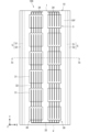
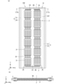
- FIG. 1 is a plan view showing an example of the external appearance of the solar cell module according to the first embodiment when viewed from above.
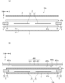
- FIG. 2 is a diagram showing an example of a hypothetical cross section of the solar cell module in FIG. 1 taken along line Ib-Ib.
- FIG. 3A is a diagram illustrating an example of the structure of the solar cell element when viewed from above on the first element surface.
- FIG. 3(b) is a diagram illustrating an example of the structure when the second element surface of the solar cell element is viewed from above.
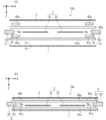
- FIGS. 4A to 4C are diagrams each illustrating a cross-sectional state during manufacture in the first specific example of the method for manufacturing a solar cell module according to the first embodiment.
- FIGS. 9A and 9B are diagrams each illustrating a cross-sectional state during manufacture in the second specific example of the method for manufacturing a solar cell module according to the first embodiment.
- FIG. 6 is a diagram illustrating a state in which the solar cell module according to the first embodiment is bent.
- FIG. 7 is a diagram showing an example of a virtual cut surface of the solar cell module according to the second embodiment.
- FIG. 8 is an enlarged view of the area surrounded by the broken line in FIG. 7.
- FIGS. 9A and 9B are diagrams each illustrating a cross-sectional state during manufacture in the first specific example of the method for manufacturing a solar cell module according to the second embodiment.
- FIGS. 9A and 9B are diagrams each illustrating a cross-sectional state during manufacture in the first specific example of the method for manufacturing a solar cell module according to the second embodiment.
- FIGS. 9A and 9B are diagrams each illustrating a cross-sectional state during manufacture in the first specific example of the method for manufacturing a solar
- FIGS. 10A and 10B are diagrams each illustrating a cross-sectional state during manufacture in a second specific example of the method for manufacturing a solar cell module according to the second embodiment.
- FIG. 11 is a diagram showing an example of a virtual cut surface of the solar cell module according to the third embodiment.
- FIGS. 12(a) and 12(b) are diagrams each illustrating a cross-sectional state during manufacturing in the method for manufacturing a solar cell module according to the third embodiment.
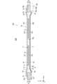
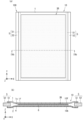
- FIG. 13A is a plan view showing an example of the external appearance of the solar cell module according to the fourth embodiment when viewed from above.
- FIG. 13(b) is a diagram showing an example of a virtual cut surface of the solar cell module of FIG. 13(a) along line IIb-IIb.
- FIG. 14 is a plan view showing an example of the external appearance of the solar cell module according to the fifth embodiment when viewed from above.
- FIG. 15A is a plan view showing an example of the external appearance of the solar cell module according to the sixth embodiment when viewed from above.
- FIG. 15(b) is a diagram illustrating an example of a hypothetical cut plane along line IIIb-IIIb of the solar cell module of FIG. 15(a).
- FIG. 16A is a diagram illustrating an example of the structure of the solar cell module according to the seventh embodiment when viewed from above.
- FIG. 16(b) is a diagram showing an example of a hypothetical cut plane along line IVb-IVb of the solar cell module of FIG. 16(a).
- FIG. 17A is a diagram illustrating an example of the structure of the solar cell section according to the seventh embodiment when viewed from above.
- FIG. 17(b) is a diagram showing an example of a hypothetical cut plane along the Vb-Vb line of the solar cell portion of FIG. 17(a).
- the inventor has created a technology that improves the flexibility and strength of solar cell modules. Regarding this, the first to seventh embodiments will be described below based on the drawings.
- FIGS. 1 to 17(b) A right-handed XYZ coordinate system is attached to FIGS. 1 to 17(b).
- the short direction of the front surface 10f of the solar panel 10 is the +X direction
- the longitudinal direction of the front surface 10f is the +Y direction
- the normal to the front surface 10f is orthogonal to both the +X direction and the +Y direction.
- the direction is the +Z direction.
- Solar cell module> A solar cell module 100 according to a first embodiment will be described based on FIGS. 1 to 3(b).
- the solar cell module 100 includes, for example, a solar cell panel 10.
- the solar cell panel 10 has, for example, a light-receiving surface (also referred to as a front surface) 10f through which light mainly enters, and a back surface 10b located on the opposite side of the front surface 10f.
- the front surface 10f is in a state facing the +Z direction.
- the back surface 10b is in a state facing the -Z direction.
- the +Z direction is set, for example, in a direction facing the sun, which is in the south.
- the front surface 10f has a rectangular shape, which is an example of a rectangular shape.
- the solar cell module 100 may further include a terminal box (not shown) for extracting the power generated by the solar cell panel 10 to the outside.
- the solar cell panel 10 includes, for example, a surface protective layer 1, a back surface protective layer 2, a solar cell section 3, a filler 4, and a support member 5. There is.
- the surface protection layer 1 has, for example, a first surface 1f and a second surface 1s (see FIG. 2).
- the first surface 1f constitutes, for example, the front surface 10f of the solar cell panel 10. That is, the surface protective layer 1 has a rectangular shape, which is an example of a rectangular shape.
- the first surface 1f is exposed to a space (also referred to as external space) 200 outside the solar cell module 100.
- the second surface 1s is a surface opposite to the first surface 1f.
- the surface protective layer 1 has, for example, translucency. Specifically, the surface protection layer 1 has, for example, transparency to light having a wavelength in a specific range.
- the specific range of wavelengths includes, for example, the wavelength of light that can be photoelectrically converted by the solar cell unit 3. If the wavelengths in the specific range include wavelengths of sunlight with high irradiation intensity, the photoelectric conversion efficiency of the solar cell module 100 can be improved.
- the surface protective layer 1 As the material of the surface protective layer 1, for example, a resin having weather resistance is applied.
- the surface protective layer 1 is made of, for example, a weather-resistant resin.
- weather resistance refers to a property that does not easily cause alterations such as deformation, discoloration, and deterioration when used outdoors, for example.
- the surface protection layer 1 reduces the intrusion of water such as water droplets from the external space 200 of the solar cell module 100 toward the solar cell section 3, and It has a property that allows moisture to easily pass from the filler 4 toward the external space 200 (also referred to as moisture-permeable waterproof property).
- the weather-resistant resin includes, for example, a fluorine-based resin.
- Fluorine-based resins include, for example, fluorinated ethylene propylene copolymer (FEP), ethylene tetrafluoroethylene copolymer (ETFE), and ethylene chlorotrifluoroethylene copolymer (Ethylene Chlorotrifluoroethylene). :ECTFE) etc.
- the surface protection layer 1 may be composed of two or more layers of resin having weather resistance.
- the fluorine-based resin applied to the surface protective layer 1 may be, for example, two or more types of resin. For this reason, for example, a mode is conceivable in which the fluororesin applied to the surface protective layer 1 includes at least one resin among FEP, ETFE, and ECTFE.
- the thickness of the surface protective layer 1 is, for example, about 0.05 millimeter (mm) to 0.5 mm.
- the surface protective layer 1 is made of a moisture permeable resin with a relatively low density and is thin, so the surface protective layer 1 is light. For this reason, the weight of the solar cell module 100 can be reduced compared to, for example, a structure in which high-density glass having a thickness of about 1 mm or more is used instead of the surface protective layer 1. can be made into a thin film.
- the material for the surface protective layer 1 resins such as acrylic resin and polycarbonate can be used instead of or together with the fluorine resin.
- the thickness of the resin is, for example, about 0.03 mm to 0.6 mm.
- the surface protection layer 1 may be formed by laminating multiple types of resins.
- the solar cell section 3 is located, for example, between the front surface protective layer 1 and the back surface protective layer 2. In other words, the solar cell section 3 is in a state opposite to the front surface protective layer 1 in the Z direction, and is also in a state opposite to the back surface protective layer 2 in the Z direction.
- the solar cell section 3 includes, for example, a plurality of solar cell elements 31.
- the plurality of solar cell elements 31 are located between the second surface 1s of the surface protection layer 1 and the back surface protection layer 2.
- the plurality of solar cell elements 31 are two-dimensionally arranged. In the examples shown in FIGS. 1 and 2, the plurality of solar cell elements 31 are arranged in a plane so as to be located along the second surface 1s of the surface protective layer 1. Note that the plurality of solar cell elements 31 may be arranged one-dimensionally.
- the solar cell section 3 further includes, for example, a plurality of first wiring members 32, a second wiring member 33, and a third wiring member 34.
- the solar cell section 3 includes, for example, a plurality of (here, two) solar cell strings 30.
- the plurality of solar cell strings 30 are arranged in the X direction.
- Each of the plurality of solar cell strings 30 includes, for example, a plurality of (here, five) solar cell elements 31 and a plurality of first wiring members 32.
- the plurality of solar cell elements 31 are arranged in the Y direction, for example.
- the plurality of first wiring members 32 are in a state of electrically connecting two mutually adjacent solar cell elements 31 among the plurality of solar cell elements 31.
- the second wiring member 33 is in a state of electrically connecting two mutually adjacent solar cell strings 30 among the plurality of solar cell strings 30 .
- two third wiring members 34 are connected to two solar cell strings 30, respectively.
- a third wiring material 34 connected to the solar cell string 30 located at the end in the -X direction and a third wiring material connected to the solar cell string 30 located at the end in the +X direction most. 34 is in a state of being pulled out to the outside of the solar cell panel 10.
- Each of the plurality of solar cell elements 31 can convert light energy into electrical energy.
- Each of the plurality of solar cell elements 31 has a surface (also referred to as a first element surface) 31f located on the front surface side and a surface (second element surface) opposite to this first element surface 31f. (also referred to as a surface) 31s.
- the first element surface 31f is in a state facing the +Z direction
- the second element surface 31s is in a state facing the -Z direction.
- the first element surface 31f primarily serves as a surface onto which light is incident (also referred to as a light-receiving surface), and the second element surface 31s primarily serves as a surface onto which light does not enter (also referred to as a non-light-receiving surface). ).
- each of the plurality of solar cell elements 31 includes a semiconductor substrate 310, a first output extraction electrode 311, and a first current collector. It has an electrode 312, a second output extraction electrode 313, and a second current collection electrode 314.
- the semiconductor substrate 310 includes, for example, a crystalline semiconductor such as crystalline silicon, an amorphous semiconductor such as amorphous silicon, four types of elements such as copper, indium, gallium, and selenium, or two types of elements such as cadmium and tellurium. Compound semiconductors using Here, it is assumed that crystalline silicon is applied to the semiconductor substrate 310.
- the semiconductor substrate 310 mainly includes a region having a first conductivity type (also referred to as a first conductivity type region) and a region having a second conductivity type opposite to the first conductivity type (a second conductivity type region). ).
- the first conductivity type region is located, for example, on the second element surface 31s side of the semiconductor substrate 310 in the ⁇ Z direction.
- the second conductivity type region is located, for example, in the surface layer portion of the semiconductor substrate 310 on the first element surface 31f side in the +Z direction.
- the semiconductor substrate 310 has a pn junction located at the interface between the first conductivity type region and the second conductivity type region.
- the thickness of the semiconductor substrate 310 is, for example, approximately 0.15 mm to 0.5 mm.
- the first output extraction electrode 311 and the first current collection electrode 312 are located, for example, on the surface of the semiconductor substrate 310 on the first element surface 31f side.
- a bus bar electrode is applied to the first output extraction electrode 311.
- a finger electrode is applied to the first current collecting electrode 312.
- five substantially parallel first output extraction electrodes 311 are located on the first element surface 31f side of the semiconductor substrate 310, and a large number of substantially parallel first current collecting electrodes 312 are located on the first element surface 31f side of the semiconductor substrate 310. , are positioned substantially perpendicular to the five first output extraction electrodes 311.
- FIG. 3A five substantially parallel first output extraction electrodes 311 are located on the first element surface 31f side of the semiconductor substrate 310, and a large number of substantially parallel first current collecting electrodes 312 are located on the first element surface 31f side of the semiconductor substrate 310. , are positioned substantially perpendicular to the five first output extraction electrodes 311.
- FIG. 3A five substantially parallel first output extraction electrodes 311
- each of the first output extraction electrodes 311 has a long shape in the Y direction, and each of the first current collecting electrodes 312 has a linear shape long in the X direction. have. Furthermore, a region on the second conductivity type region of the semiconductor substrate 310 where the first output extraction electrode 311 and the first current collecting electrode 312 are not formed is made of, for example, silicon nitride. An insulating film may be provided as a certain anti-reflection film 315.
- the main component of the first output extraction electrode 311 is silver
- the first output extraction electrode 311 is formed by applying silver paste into a desired shape by screen printing or the like and then firing it. can be formed.
- main component refers to a component that has the largest (highest) ratio (also referred to as content) among the contained components.
- a metal paste containing a metal powder containing silver as a main component, an organic vehicle, and a glass frit is applied to the silver paste.
- the first current collecting electrode 312 is silver
- the first current collecting electrode 312, like the first output extraction electrode 311 is made by applying silver paste into a desired shape by screen printing or the like. It can be formed by later firing.
- the first output extraction electrode 311 and the first current collection electrode 312 may be formed in separate processes, or may be formed in the same process.
- the second output extraction electrode 313 and the second current collection electrode 314 are located, for example, on the surface of the semiconductor substrate 310 on the second element surface 31s side.
- a bus bar electrode is applied to the second output extraction electrode 313.
- five rows of second output extraction electrodes 313 that are substantially parallel to each other along the +Y direction are located on the second element surface 31s side of the semiconductor substrate 310.
- the second current collecting electrode 314 is located on the second element surface 31s side of the semiconductor substrate 310, except for a portion where the second output extraction electrode 313 and the second current collecting electrode 314 are overlapped and connected to each other. It is located almost on the entire area where the two-output extraction electrode 313 is not formed.
- Each of the five rows of second output extraction electrodes 313 includes, for example, four electrodes arranged in a row. Further, for example, a passivation film is formed between the first conductivity type region of the semiconductor substrate 310 and the second output extraction electrode 313 and the second current collecting electrode 314 by forming a thin film of oxide or nitride such as aluminum oxide in a desired pattern. may exist as .
- the main component of the second output extraction electrode 313 is silver
- the second output extraction electrode 313, like the first output extraction electrode 311 can be formed by applying silver paste into the desired shape by screen printing or the like. It can be formed by being fired after being applied.
- the second current collecting electrode 314 may be formed by applying aluminum paste into a desired shape by screen printing or the like and then firing it.
- aluminum paste containing a metal powder containing aluminum as a main component, an organic vehicle, and a glass frit is applied to the aluminum paste.
- the first wiring material 32 connects, for example, a first output extraction electrode 311 of one solar cell element 31 and a second output extraction electrode 313 of another solar cell element 31 adjacent to this one solar cell element 31. are electrically connected.
- the outer edges of the plurality of first wiring members 32 attached to each of the solar cell elements 31 are virtually drawn with two-dot chain lines.
- the first wiring member 32 has an elongated shape that is long in the Y direction.
- the first wiring material 32 is in a state of being joined to the first output extraction electrode 311 and the second output extraction electrode 313, for example.
- a portion (a first (also referred to as a joint portion) 321 exists. Therefore, for example, the first wiring material 32 is in a state of being joined to the first output extraction electrode 311 of one solar cell element 31 via the first joint portion 321. Also, for example, a portion located between the first wiring material 32 and the second output extraction electrode 313 and joining the first wiring material 32 and the second output extraction electrode 313 (also referred to as a second joint portion) 322 exists. Therefore, for example, the first wiring material 32 is in a state where it is joined to the second output extraction electrode 313 of another solar cell element 31 adjacent to one solar cell element 31 via the second joint portion 322. It is in.
- the first wiring material 32 for example, a linear or band-shaped electrically conductive metal body is applied.
- a low melting point alloy such as solder or a low melting point single metal is applied. More specifically, for example, a copper foil having a thickness of about 0.1 mm to 0.2 mm and a width of about 1 mm to 2 mm is applied to the first wiring material 32, and solder is applied to the entire surface of the first wiring material 32. is covered.
- the first wiring material 32 is in a state of being electrically connected to the first output extraction electrode 311 and the second output extraction electrode 313, for example, by soldering.
- the solder located between the first wiring material 32 and the first output extraction electrode 311 constitutes the first joint portion 321. Further, for example, the solder located between the first wiring material 32 and the second output extraction electrode 313 constitutes the second joint portion 322 .
- the filler 4 is in a state covering the solar cell part 3 between the front protection layer 1 and the back protection layer 2. In other words, the filler 4 is in a state covering the plurality of solar cell elements 31 between the front protective layer 1 and the back protective layer 2. From another point of view, the filler 4 is filled in, for example, a region (also referred to as a gap region) 10g between the surface protective layer 1 and the back surface protective layer 2 while covering the solar cell section 3. be.
- the filler 4 has a first surface 4f located on the front surface, and a second surface 4s located on the opposite side to the first surface 4f.
- the first surface 4f of the filler 4 is in contact with the second surface 1s of the surface protection layer 1, and the second surface 4s of the filler 4 is in contact with the back surface protection layer 2.
- the filler 4 includes, for example, a filler (also referred to as a first filler) 41 located on the front surface 10f side and a filler (also referred to as a second filler) located on the back surface 10b side. 42).
- the first filler 41 is in a state of forming, for example, the first surface 4f, and is in a state of covering the entire surface of the solar cell section 3 on the surface protection layer 1 side. In other words, the first filler 41 is in a state of covering the plurality of solar cell elements 31, for example, between the surface protection layer 1 and the plurality of solar cell elements 31.
- the second filler 42 is in a state of forming, for example, the second surface 4s, and is in a state of covering the entire surface of the solar cell section 3 on the back surface protective layer 2 side.
- the second filler 42 is in a state of covering the plurality of solar cell elements 31, for example, between the back surface protective layer 2 and the plurality of solar cell elements 31. Therefore, in the first embodiment, the solar cell section 3 is in a state of being sandwiched and surrounded by the first filler 41 and the second filler 42, for example. Thereby, for example, the attitude of the solar cell section 3 can be maintained by the filler 4.
- the filler 4 has, for example, translucency.
- the filler 4 has, for example, translucency to light having a wavelength in the above-mentioned specific range.
- the incident light from the front surface 10f side can reach up to the solar cell section 3.
- the material for the first filler 41 for example, ethylene vinyl acetate copolymer (EVA), polyvinyl acetal such as polyvinyl butyral (PVB), acid-modified resin, etc. are used.
- EVA ethylene vinyl acetate copolymer
- PVB polyvinyl acetal
- acid-modified resin etc.
- the acid-modified resin includes, for example, a modified polyolefin resin that can be formed by graft modification of a resin such as polyolefin with an acid.
- acids that can be used for graft modification of acid-modified resins include acrylic acid, methacrylic acid, maleic acid, fumaric acid, itaconic acid, maleic anhydride, hymic anhydride, itaconic anhydride, and citraconic anhydride.
- Ru As the material for the second filler 42, for example, like the first filler 41, polyvinyl acetal such as EVA and PVB, acid-modified resin, etc. are used.
- the first filler 41 and the second filler 42 may be made of two or more types of materials, for example.
- the second filler 42 may contain, for example, a pigment.
- a white pigment included, the light transmitted through the solar cell section 3 can be reflected by the second filler 42 and made to enter the solar cell section 3 again. Thereby, the power generation efficiency of the solar cell module 100 can be improved.
- the filler 4 may not include the second filler 42 and may include only the first filler 41.
- the first filler 41 covers the solar cell section 3 between the front protective layer 1 and the back protective layer 2.
- the back surface protective layer 2 is in a state of forming the back surface 10b of the solar cell panel 10, for example.
- the back surface protective layer 2 is in a state facing the second surface 1s of the surface protective layer 1.
- the back surface protective layer 2 is in contact with the filler 4 on the side opposite to the surface protective layer 1 with respect to the filler 4 .
- the back surface protective layer 2 is located facing the solar cell portion 3 and the inner portion 51 of the support member 5 in the Z direction.
- the inner portion 51 is a portion of the support member 5 on the solar cell section 3 side with respect to the outer portion 52 in the X direction.
- the back surface protective layer 2 can, for example, protect the solar cell section 3 from the back surface 10b side.
- a back sheet forming the back surface 10b is applied to the back surface protective layer 2.
- the thickness of the back sheet is, for example, about 0.15 mm to 0.5 mm.
- resin is used as the material for the back sheet.
- the same material as the surface protective layer 1 can be applied to the resin.
- the back surface protective layer 2 has the same or similar shape to the surface protective layer 1 when viewed in plan from the back surface 10b side. For example, a configuration is assumed in which both the surface protective layer 1 and the back surface protective layer 2 have a rectangular outer shape when viewed from the back surface 10b side.
- the support member 5 is a member for improving the rigidity of the solar cell panel 10, and has higher rigidity than all of the surface protection layer 1, back surface protection layer 2, and filler 4, for example.
- metal can be used as the material of the support member 5, and as a more specific example, aluminum or stainless steel can be used.
- the support member 5 is located adjacent to the solar cell section 3 with an interval when viewed from above toward the main surface of the surface protection layer 1. In other words, the support member 5 is located adjacent to the solar cell section 3 with an interval when viewed with the line of sight along the Z direction. Hereinafter, viewing with the line of sight along the Z direction will also simply be referred to as planar viewing.
- the support member 5 includes an inner portion 51 and an outer portion 52, and the inner portion 51 is located between the front protective layer 1 and the back protective layer 2 and covered with the filler 4. There is. In other words, the inner portion 51 is in a state opposite to the front surface protective layer 1 in the Z direction, is in a state opposite to the back surface protective layer 2 in the Z direction, and is in a state covered by the filler 4.
- the outer portion 52 extends from the inner portion 51 to the side opposite to the solar cell portion 3 (that is, to the outside), and is not covered with the filler 4, for example.
- the outer portion 52 extends from the inner portion 51 to the outside of the front protective layer 1 and the back protective layer 2 in plan view. That is, the outer portion 52 is in a state where it is not facing the front surface protective layer 1 in the Z direction, and is also not facing the back surface protective layer 2 in the Z direction.
- the inner portion 51 of the support member 5 is located on the solar cell section 3 side (that is, inside) with respect to the outer portion 52 of the support member 5 in plan view.
- the support member 5 has a plate-like shape, and has a rectangular shape in plan view.
- the ZX cross section of the support member 5 also has a rectangular shape.
- the corners of the support member 5 may be chamfered as appropriate.
- the longitudinal direction (here, the Y direction) of the support member 5 is, for example, along one side of the surface protection layer 1. Further, the longitudinal direction of the support member 5 is, for example, along the arrangement direction (here, the Y direction) of the plurality of solar cell elements 31 included in one solar cell string 30. That is, the longitudinal direction of the support member 5 is along, for example, the longitudinal direction of the first wiring member 32 (here, the Y direction).
- the solar panel 10 includes two support members 5.
- the two support members 5 are located along both sides of the surface protection layer 1 on both sides in the X direction.
- the two sides located on both sides of the X direction herein refer to one side of the surface protective layer 1 extending along the Y direction at the end in the -X direction, and one side extending along the Y direction at the end in the +X direction. and one extending side. That is, one support member 5 is located at the end of the surface protection layer 1 in the -X direction and has a rectangular shape with the longitudinal direction being the Y direction, and the other support member 5 is located at the end of the surface protection layer 1 in the -X direction. 1, and has a rectangular shape whose longitudinal direction is the Y direction.
- the length of the support member 5 in the longitudinal direction is, for example, approximately equal to the length of the surface protection layer 1.
- the width of the support member 5 in the transverse direction (here, the X direction) is set to, for example, several tens of mm or more.
- the width of the inner portion 51 of the support member 5 is set to, for example, approximately 20% or more and 80% or less of the width of the support member 5.
- the thickness of the support member 5 is larger than the thickness of the solar cell section 3, and is set to about 1 mm to 5 mm, for example.
- the outer portion 52 of the support member 5 is attached to an attachment target member such as an external building material.
- outer portion 52 may be formed with mounting holes (not shown).
- the mounting hole passes through the outer portion 52 in the Z direction.
- the solar cell panel 10 can be attached to the attachment target member by passing the mounting bolt through the attachment hole and screwing into the attachment target member.
- the two support members 5 are located on both sides of the solar panel 10, so it is possible to fix the two support members 5 on both sides of the solar panel 10 to the attachment target member. can. Therefore, the solar cell panel 10 can be more firmly attached to the attachment target member. It can also be said that the support member 5 is a mounting member.
- the support members 5, which are rigid bodies, are not mainly located on both sides of the solar cell panel 10 in the Y direction. That is, the support member 5 is not substantially located at the end of the solar cell panel 10 in the +Y direction and extends along the X direction, but is located at the end of the solar cell panel 10 in the -Y direction. It is not substantially located at the end portion extending along the X direction either. Therefore, as shown in FIG. 6, by applying the external force F1 to the support member 5, the solar cell panel 10 can be bent in an arc shape when viewed in the direction along the Y direction. In other words, the solar cell panel 10 can be bent in an arc shape when viewed with the line of sight along the Y direction. For example, the solar cell panel 10 can be bent to a state along an arc with a radius of about several hundred mm (for example, 500 mm). According to this, it is easy to attach the solar cell panel 10 to the curved attachment target member.
- the distance between the front protective layer 1 and the back protective layer 2 is small in the solar cell section 3, and the distance between the solar cell section 3 and the support member 5 is small. Large in size. In other words, the distance (maximum value) between the front protective layer 1 and the back protective layer 2 between the solar cell section 3 and the support member 5 is the same as the distance between the front protective layer 1 and the back protective layer 2 in the solar cell section 3. (maximum value).
- the portion 4a referred to here is a portion of the filler 4 that is located between the solar cell section 3 and the support member 5 and is located continuously from the surface protective layer 1 to the back surface protective layer 2. .
- the thickness W1 of the portion 4a at the end on the support member 5 side is larger than the thickness W2 of the portion 4a at the end on the solar cell section 3 side.
- the difference between the thickness W1 and the thickness W2 may be, for example, 0.1 mm or more, 0.5 mm or more, or 1 mm or more.
- the thickness of the portion 4a of the filler 4 is, for example, in at least a partial region R1 between the support member 5 and the solar cell portion 3, from the solar cell portion 3 along the X direction. It gradually increases toward the support member 5. That is, the thickness of the portion 4a of the filler 4 increases monotonically in the region R1 from the solar cell portion 3 toward the support member 5 along the X direction. In other words, as the position in the X direction approaches the support member 5 from the solar cell section 3, the thickness of the portion 4a of the filler 4 at that position gradually increases. In short, the thickness of the portion 4a gradually increases in the region R1 toward the outside along the X direction.
- the amount of increase in the thickness of the entire region R1 may be, for example, 0.1 mm or more, 0.5 mm or more, or 1 mm or more.
- the shape of the portion 4a of the filler 4 is, for example, uniform in the Y direction.
- the first surface 4f and the second surface 4s of the filler 4 have shapes that are line symmetrical to each other with respect to the XY plane, but the drawing is shown schematically. However, it is not necessarily limited to this.
- the inner portion 51 of the support member 5, which is a rigid body, is covered with the filler 4 between the front protection layer 1 and the back protection layer 2. Therefore, the rigidity of the solar cell panel 10 can be improved.
- the support member 5 is located at the end of the solar cell panel 10 in the X direction and between both ends of the solar cell panel 10 in the Y direction, so that the rigidity in the Y direction is particularly improved. be able to.
- the support members 5 are not substantially located on both sides of the solar cell panel 10 in the Y direction. That is, the support member 5 is not substantially located at the end of the solar cell panel 10 in the +Y direction and extends along the X direction, but is located at the end of the solar cell panel 10 in the -Y direction. It is not substantially located at the end portion extending along the X direction either. Therefore, when viewed with the line of sight along the Y direction, the solar cell panel 10 can be bent in an arc shape (see FIG. 6). In such a bent state, a relatively large stress is generated in the portion of the solar cell panel 10 between the support member 5 and the solar cell section 3. More specifically, a large stress is generated in a portion of the solar cell panel 10 near the inner end surface 5a of the support member 5.
- the inner end surface 5a here is the end surface of the support member 5 on the solar cell section 3 side.
- the thickness of the filler 4 is large between the support member 5 and the solar cell part 3 and is small in the solar cell part 3.
- the thickness W1 is larger than the thickness W3. Therefore, the strength of the solar cell panel 10 can be improved between the support member 5 and the solar cell section 3. Therefore, the solar cell panel 10 can appropriately cope with stress due to bending.
- the filler 4 is thin in the solar cell section 3, the flexibility of the solar cell panel 10 can be improved. In other words, it is possible to achieve both flexibility and strength of the solar cell panel 10.
- the volume of the filler 4 can be made smaller compared to a structure in which the thickness W3 is increased to the same extent as the thickness W1, the material cost of the filler 4 can also be reduced.
- the thickness W1 of the portion 4a of the filler 4 is larger than the thickness W2, the strength of the solar cell panel 10 can be improved near the inner end surface 5a of the support member 5. Therefore, the solar cell panel 10 can more appropriately cope with the stress caused by the bending. Further, in the region R1, if the thickness of the portion 4a gradually increases from the solar cell portion 3 toward the support member 5, stress in the portion 4a can be effectively dispersed.
- the surface protective layer 1 is prepared.
- a resin film having rectangular front and back surfaces and weather resistance is prepared as the surface protection layer 1.
- a fluorine-based resin is used as the weather-resistant resin.
- the fluorine-based resin for example, FEP, ETFE, or ECTFE is used.
- the second surface 1s which is one surface of the surface protective layer 1, is subjected to a treatment for activating the surface, such as corona treatment or plasma treatment. Thereby, the adhesion between the surface protection layer 1 and the filler 4 can be improved in the lamination process described below.
- the surface protective layer 1 the sheet 41s, the sheet 41t, the solar cell part 3, the support member 5, the sheet 42s, the sheet 42t, and the back surface protection
- a stacked body 10s is formed.
- the solar cell section 3 is located between two support members 5, and these are arranged in a spaced-apart manner in the X direction. Further, at this time, wiring is appropriately positioned to be drawn out from the solar cell section 3 to the outside of the solar cell panel 10 and connected to a terminal box or the like.
- the plurality of solar cell elements 31 of the solar cell section 3 are connected to each other by a first wiring material 32 and a second wiring material 33. Further, the third wiring member 34 is connected to the solar cell section 3 .
- the sheet 41s and the sheet 41t are sheets made of resin (such as EVA) that is the base material of the first filler 41.
- the sheet 41s is located between the surface protection layer 1 and the solar cell section 3 and between the surface protection layer 1 and the support member 5. That is, the sheet 41s is located on the surface protection layer 1, and the solar cell section 3 and the support member 5 are located on the sheet 41s.
- the sheet 41s has a rectangular shape as an example of a rectangular shape in plan view.
- the sheet 41t is located between the support member 5 and the solar cell section 3 and above the sheet 41s.
- two support members 5 are located, so two sheets 41t are located.
- each sheet 41t has, for example, an elongated shape that is long in the Y direction.
- the width of each sheet 41t is narrower than the distance between the support member 5 and the solar cell section 3. That is, in the examples of FIGS. 4(b) and 4(c), the sheet 41t is located in a state where it does not face both the support member 5 and the solar cell section 3 in the Z direction.
- the sheet 42s and the sheet 42t are sheets made of resin (such as EVA) that is the base material of the second filler 42.
- the sheet 42s and the sheet 42t may contain pigment.
- the sheet 42s is located between the back protection layer 2 and the solar cell section 3 and between the back protection layer 2 and the support member 5. In other words, the sheet 42s is positioned with both ends facing the support member 5, respectively.
- the sheet 42s has a rectangular shape as an example of a rectangular shape in plan view.
- the sheet 42t is located between the support member 5 and the solar cell section 3 and above the sheet 42s.
- two support members 5 are located, so two sheets 42t are located.
- each sheet 42t has, for example, an elongated shape that is long in the Y direction.
- the width of each sheet 42t is narrower than the distance between the support member 5 and the solar cell section 3. That is, in the examples shown in FIGS. 4(b) and 4(c), the sheet 42t is positioned so as not to face both the support member 5 and the solar cell section 3 in the Z direction.
- the back surface protective layer 2 is located on the sheet 42s and the sheet 42t.
- the sheet 41t and the sheet 42t are located between the support member 5 and the solar cell section 3 in plan view. Therefore, the total thickness of the sheet between the support member 5 and the solar cell section 3 is larger than the total thickness of the sheet in the region facing the solar cell section 3 by the amount of the sheet 41t and the sheet 42t.
- the sheet 42s and the back protective layer 2 are shown in a flat plate shape, if they are flexible or pliable, the central part of the sheet 42s and the back protective layer 2 will be the surface protective layer. It can bend to one side.
- a lamination process is performed on the laminate 10s.
- a laminate device (laminator) is used to integrate the laminate 10s.
- the laminate 10s is placed on a heater board in a chamber, and while the pressure inside the chamber is reduced from 50 Pascals (Pa) to about 150 Pa, the laminate 10s is heated from 100 degrees Celsius (100 degrees Celsius) to 200 degrees Celsius. Heat to about 200°C.
- the sheets 41s, 41t, 42s, and 42t become fluidized to some extent by heating.
- the laminate 10s is pressed in the Z direction with a pressing member such as a diaphragm sheet, thereby integrating the laminate 10s.
- the sheet 41t and the sheet 42t are located in the laminate 10s.
- the total thickness of the sheet increases between the support member 5 and the solar cell section 3. Therefore, the thickness of the filler 4 between the support member 5 and the solar cell section 3 can be increased more easily.
- the sheets 41t and 42t are located, a gap due to the difference in thickness between the support member 5 and the solar cell element 31 will be created between the support member 5 and the solar cell part 3 of the laminate 10s. can be reduced.
- the pressing body of the laminator can press the laminate 10s with sufficient pressure even between the support member 5 and the solar cell section 3.
- unevenness in pressure distribution caused by the difference in thickness between the support member 5 and the solar cell element 31 can be reduced. Therefore, the molten sheet is pressed against the surface protection layer 1, the support member 5, the solar cell section 3, and the back surface protection layer 2 with sufficient pressure even between the support member 5 and the solar cell section 3.
- the filler 4 can be bonded to these with higher adhesive strength.
- the sheet 42t is located above the sheet 42s in the lamination process, but it may be located between the sheet 42s and the sheet 41t.
- the sheet 41t is located on the sheet 41s, it may be located between the sheet 41s and the surface protection layer 1.
- a plurality of sheets 41t may be stacked in the Z direction, or a plurality of sheets 42t may be stacked in the Z direction. Further, only one of the sheet 41t and the sheet 42t may be located.
- the sheet 41s and the sheet 41t are separate sheets in the above example, they may be integrated. That is, the thickness of the sheet in the region between the support member 5 and the solar cell section 3 only needs to be larger than the thickness of the sheet in the region facing the solar cell section 3. The same applies to the sheet 42s and the sheet 42t.
- a terminal box or the like may be attached to the solar cell panel 10 as appropriate.
- wiring drawn out from the solar cell section 3 to the outside of the solar cell panel 10 is appropriately connected to a terminal in the terminal box. Thereby, the solar cell module 100 is assembled.
- the solar cell panel 10 including the support member 5 is integrated by lamination processing. Therefore, the solar cell panel 10 is easier to assemble than a structure in which an external frame (not shown) is attached to the solar cell panel 10 with screws or the like instead of the support member 5.
- the sheets 41t and 42t may not be located in the laminate 10s.
- the pressing surface 400s of the pressing body 400 of the laminator may have a stepped shape.
- the pressing surface 400s is a surface that contacts the laminate 10s and presses the laminate 10s.
- the pressing body 400 includes a diaphragm sheet 410, a first release sheet 420, and a second release sheet 421.
- the material of the diaphragm sheet 410 is, for example, an elastic member such as silicone rubber that is easily elastically deformable.
- the diaphragm sheet 410 is wider than the stacked body 10s in plan view, and is positioned facing the entire stacked body 10s.
- the first release sheet 420 is a sheet that has release properties.
- the first release sheet 420 is obtained, for example, by forming a release film such as a silicone coating on the surface of a sheet-like base material.
- the first release sheet 420 is located on the laminate 10s side with respect to the diaphragm sheet 410.
- the first release sheet 420 is positioned to overlap the diaphragm sheet 410.
- the first release sheet 420 is wider than the laminate 10s in plan view, and is positioned facing the entire laminate 10s.
- the second release sheet 421 is a sheet that has release properties.
- the second release sheet 421 is obtained, for example, by forming a release film such as a silicone coating on the surface of a sheet-like base material.
- the second release sheet 421 is located on the laminate 10s side with respect to the first release sheet 420.
- the second release sheet 421 is positioned to overlap the first release sheet 420.
- the second release sheet 421 has, for example, an elongated shape that is long in the Y direction in plan view.
- the width of the second release sheet 421 in the X direction is narrower than the interval between the two supporting members 5 and is greater than or equal to the width of the solar cell section 3 .
- the second release sheet 421 is in a state where it faces the laminate 10s in the Z direction between the two support members 5, and does not face the support member 5 in the Z direction. Further, the second release sheet 421 is in a state facing the entire solar cell section 3 in the Z direction.
- the length of the second release sheet 421 in the Y direction is, for example, longer than the length of the laminate 10s in the Y direction.
- the pressing surface 400s which is the surface of the pressing body 400 on the laminate 10s side, has a step on both sides of the second release sheet 421, and the second release sheet 421 of the pressing surface 400s The portion corresponding to the second release sheet 421 protrudes toward the laminate 10s by the thickness of the second release sheet 421.
- the pressing surface 400s includes a first region 401s facing the support member 5, and a second region 402s located closer to the laminate 10s than the first region 401s and corresponding to the solar cell section 3.
- the step between the first region 401s and the second region 402s is located between the support member 5 and the solar cell section 3 in the X direction.
- the pressing surface 400s of such a pressing body 400 has a stepped shape corresponding to the thickness distribution of the filler 4 illustrated in FIG. 2 .
- the pressing body 400 initially presses the back protective layer 2 in the second area (that is, the second release sheet 421) facing the solar cell part 3, and then presses the back protective layer 2 in the second area facing the solar cell part 3 (that is, the second release sheet 421), and then Press the back protective layer 2 in one area. Therefore, the molten sheet easily flows toward the support member 5 and flows between the support member 5 and the solar cell section 3. Therefore, the thickness of the filler 4 between the support member 5 and the solar cell section 3 can be easily increased.
- the pressing body 400 has a more uniform pressure distribution.
- the laminated body 10s can be pressed with. As a result, even between the support member 5 and the solar cell part 3, the filler 4 adheres to the surface protection layer 1, the support member 5, the solar cell part 3, and the back protection layer 2 with higher adhesive strength. be able to.
- the thickness W1 of the filler 4 between the support member 5 and the solar cell section 3 is larger than the thickness W3 of the filler 4 between the solar cell elements 31, for example. Therefore, the strength of the solar cell panel 10 can be increased between the support member 5 and the solar cell section 3. As a result, the solar cell panel 10 can withstand the stress applied to the portion between the support member 5 and the solar cell section 3 due to the deflection due to the external force F1. Moreover, since the thickness W3 is small, the flexibility of the solar cell panel 10 can be improved.
- the number of solar cell elements 31 arranged in the X direction is 2, which is an even number.
- the number of solar cell elements 31 arranged in the direction orthogonal to the longitudinal direction of the support member 5 is an even number.
- the widths of each solar cell element 31 in the X direction are substantially equal to each other. Therefore, the solar cell element 31 does not exist at the center of the solar cell panel 10 in the X direction. That is, the center of the solar cell panel 10 corresponds to the portion between the solar cell elements 31.
- the solar cell panel 10 when the solar cell panel 10 is bent by the external force F1 (see also FIG. 6), a relatively large stress is also applied to the center of the solar cell panel 10 in the X direction. Further, even when a load such as snow is applied to the solar cell panel 10 while the support member 5 is attached to the attachment target member, the solar cell panel 10 can bend in an arc shape when viewed in the Y direction. Even in such a case, a relatively large stress is applied to the center of the solar cell panel 10 in the X direction.
- no solar cell element 31 is present at the center of the solar cell panel 10. Therefore, even when the solar cell panel 10 is bent due to the external force F1 or a load such as snow accumulation being applied to the solar cell panel 10, the stress applied to each solar cell element 31 is relatively small. Therefore, it is possible to reduce the possibility that problems such as performance deterioration of the solar cell element 31 due to stress will occur.
- the portion 4b of the filler 4 between the support member 5 and the surface protection layer 1 (corresponding to the first portion) is as follows. (corresponding to a predetermined first thickness distribution).
- the first thickness distribution is a thickness distribution in which the thickness W4 at the end of the portion 4b on the solar cell section 3 side is larger than the thickness W5 at the end of the portion 4b on the outer portion 52 side.
- the difference between the thickness W4 and the thickness W5 may be, for example, 0.01 mm or more, 0.05 mm or more, or 0.1 mm or more.
- the thickness of the portion 4b of the filler 4 gradually increases from the inner end surface 5a toward the outer end surface 5b at least in region R2 of the region facing the support member 5 in the Z direction. It may be reduced to
- the outer end surface 5b here is the end surface of the support member 5 on the opposite side to the solar cell section 3 in the X direction. It can also be said that the thickness of the portion 4b may decrease monotonically from the inner end surface 5a toward the outer end surface 5b in the region R2.
- the amount of reduction in thickness in the entire area R2 may be, for example, 0.01 mm or more, 0.05 mm or more, or 0.1 mm or more.
- the thickness of the portion 4a of the filler 4 gradually increases from the solar cell section 3 toward the support member 5, and the thickness of the portion 4b of the filler 4 increases from the inner end surface 5a to the outer end surface. It gradually decreases toward 5b. Therefore, the first surface 4f of the filler 4 has a convex shape that bulges in the +Z direction near the inner end surface 5a of the support member 5. Specifically, the first surface 4f is, for example, bulged in a smooth mountain shape.
- the shapes of the portions 4a and 4b of the filler 4 are uniform in the Y direction, for example.
- a portion 4c of the filler 4 between the support member 5 and the back protective layer 2 also has a thickness distribution (second thickness) described below. distribution).
- the second thickness distribution is a thickness distribution in which the thickness W6 at the end of the portion 4c on the solar cell section 3 side is larger than the thickness W7 at the end of the portion 4c on the outer portion 52 side.
- the difference between the thickness W6 and the thickness W7 may be, for example, 0.01 mm or more, 0.05 mm or more, or 0.1 mm or more.
- the thickness of the portion 4c of the filler 4 gradually increases from the inner end surface 5a toward the outer end surface 5b at least in the region R3 of the region facing the support member 5 in the Z direction. May be reduced. In other words, the thickness of the portion 4c may decrease monotonically from the inner end surface 5a toward the outer end surface 5b in the region R3.
- the amount of reduction in the thickness of the entire region R3 may be, for example, 0.01 mm or more, 0.05 mm or more, or 0.1 mm or more.
- the second surface 4s of the filler 4 has a convex shape that bulges in the -Z direction near the inner end surface 5a of the support member 5. Specifically, the second surface 4s is, for example, bulged in a smooth mountain shape.
- the shape of the portion 4c of the filler 4 is, for example, uniform in the Y direction.
- the explanation will focus on the distance between the front protective layer 1 and the back protective layer 2. That is, the distance between the front protective layer 1 and the back protective layer 2 at the inner end surface 5a of the support member 5 is the same as the distance between the front protective layer 1 and the back protective layer 2 at the end of the front protective layer 1 in the X direction or the end of the back protective layer 2 in the X direction. The distance is wider than the distance between the protective layer 1 and the back surface protective layer 2. The distance between the front protective layer 1 and the back protective layer 2 is maximum near the inner end surface 5a of the support member 5.
- the description will focus on the thickness of the structure consisting of the filler 4 and the support member 5. That is, the thickness of the structure at the position of the inner end surface 5a of the support member 5 is larger than the thickness of the structure at the end of the front protective layer 1 in the X direction or the end of the back protective layer 2 in the X direction. . The thickness of the structure is maximum near the inner end surface 5a of the support member 5.
- the thickness W4 of the portion 4b of the filler 4 is larger than the thickness W5. Therefore, the thickness of the solar cell panel 10 near the inner end surface 5a of the support member 5 can be further increased, and the strength of the solar cell panel 10 near the inner end surface 5a can be further improved. Therefore, even if the external force F1 is increased and the solar cell panel 10 is deflected more, the solar cell panel 10 can withstand the stress. Further, since the thickness W5 of the filler 4 is smaller than the thickness W4, the material cost of the filler 4 can be reduced compared to a structure in which the thickness W5 of the filler 4 is increased to the same extent as the thickness W4.
- the thickness W6 of the portion 4c of the filler 4 is larger than the thickness W7. Therefore, the thickness of the solar cell panel 10 near the inner end surface 5a of the support member 5 can be further increased, and the strength of the solar cell panel 10 near the inner end surface 5a can be further improved. Therefore, even if the external force F1 is increased and the solar cell panel 10 is deflected more, the solar cell panel 10 can withstand the stress. Further, since the thickness W7 of the filler 4 is smaller than the thickness W6, the material cost of the filler 4 can be reduced compared to a structure in which the thickness W7 of the filler 4 is increased to the same extent as the thickness W6.
- first surface 4f and the second surface 4s of the filler 4 have shapes that are line symmetrical to each other with respect to the XY plane, but the drawings are not shown schematically. However, this is not necessarily the case.
- the thickness of either the portion 4b or the portion 4c of the filler 4 may be uniform.
- either the portion 4b or the portion 4c may have a flat plate shape with a uniform thickness. This is because if either the portion 4b or the portion 4c has the above-mentioned thickness distribution, the strength of the solar cell panel 10 can be improved in the vicinity of the inner end surface 5a.
- the surface protective layer 1 the sheet 41s, the sheet 41u, the solar cell part 3, the support member 5, the sheet 42s, the sheet 42u, and the back surface protective layer 2.
- a stacked body 10s is formed. That is, compared to the first specific example of the first embodiment, sheets 41u and 42u are used instead of sheets 41t and 42t, respectively.
- the sheet 41u is a sheet made of resin (such as EVA) that is a base material of a part of the first filler 41.
- the sheet 41u is located above the sheet 41s.
- each sheet 41u has, for example, an elongated shape that is long in the Y direction.
- the sheet 41u is located in a region spanning the inner end surface 5a of the support member 5 in the X direction.
- the outer part of the sheet 41u in the X direction is located between the surface protection layer 1 and the support member 5, and the inner part of the sheet 41u in the X direction is located inside the inner end surface 5a of the support member 5. ing.
- the inner portion of this sheet 41u is located, for example, in a state where it does not face the solar cell section 3 in the Z direction.
- the outer end of the sheet 41u in the X direction is located inside, for example, with respect to the end of the surface protective layer 1 and the end of the sheet 41s in the X direction.
- the sheet 42u is a sheet made of resin (such as EVA) that forms part of the second filler 42.
- the sheet 42u is located above the sheet 42s.
- two support members 5 are located, so two sheets 42u are located.
- each sheet 42u has, for example, an elongated shape that is long in the Y direction.
- the sheet 42u is located in a region spanning the inner end surface 5a of the support member 5 in the X direction. That is, the outer part of the sheet 42u in the X direction is located between the back protective layer 2 and the support member 5, and the inner part of the sheet 42u in the X direction is located inside the inner end surface 5a of the support member 5. ing.
- the inner portion of this sheet 42u is located, for example, in a state where it does not face the solar cell section 3 in the Z direction. Further, the outer end of the sheet 42u in the X direction is located inside, for example, with respect to the end of the back protective layer 2 and the end of the sheet 42s in the X direction.
- a lamination process is performed on the laminate 10s.
- a laminate device laminated to integrate the laminate 10s.
- the solar cell panel 10 shown in FIGS. 7 and 8 can be manufactured.
- the sheet 41u is positioned so as to straddle the inner end surface 5a of the support member 5. Therefore, the thickness W4 of the portion 4b of the filler 4 can be increased more easily. Further, in plan view, the outer end of the sheet 41u is located inside the end of the surface protective layer 1 and the end of the sheet 41s, so that the thickness W5 of the portion 4b can be more easily reduced than the thickness W4. be able to.
- the sheet 42u is positioned so as to straddle the inner end surface 5a of the support member 5. Therefore, the thickness W6 of the portion 4c of the filler 4 can be increased more easily. Further, in plan view, the outer end of the sheet 42u is located inside the end of the back protective layer 2 and the end of the sheet 41s, so that the thickness W7 of the portion 4c can be more easily reduced than the thickness W6. be able to.
- the sheet 41u and the sheet 42u may not be located in the laminate 10s.
- the pressing surface 400s of the pressing body 400 may have a stepped shape.
- the pressing body 400 further includes a third release sheet 422, compared to the pressing body 400 of FIG. 5(b).
- the third release sheet 422 is a sheet that has release properties.
- the third release sheet 422 is obtained, for example, by forming a release film such as a silicone coating on the surface of a sheet-like base material.
- the third release sheet 422 is located on the laminate 10s side with respect to the first release sheet 420.
- the third release sheet 422 is positioned to overlap the first release sheet 420.
- the third release sheet 422 has, for example, an elongated shape that is elongated in the Y direction, and is positioned to face the end of the back surface protective layer 2 in the X direction in the Z direction.
- An inner end 422a of the third release sheet 422 on the second release sheet 421 side is located between the end of the back protective layer 2 and the inner end surface 5a of the support member 5 in the X direction.
- An outer end 422b of the third release sheet 422 on the opposite side to the second release sheet 421 is located outside of the end of the back protective layer 2 in the X direction.
- the pressing surface 400s of the pressing body 400 has a concave shape that is recessed in a region facing the vicinity of the inner end surface 5a of the support member 5 in the Z direction. More specifically, the pressing surface 400s includes a first region 401s that faces the inner end surface 5a of the support member 5, and a second region that is located closer to the laminate 10s than the first region 401s and that faces the solar cell section 3. It has a region 402s and a third region 403s located closer to the stacked body 10s than the first region 401s and facing the end of the back surface protective layer 2.
- the pressing surface 400s of such a pressing body 400 has a stepped shape according to the thickness distribution of the filler 4 illustrated in FIGS. 7 and 8.
- such a pressing body 400 presses regions of the back protective layer 2 at both ends in the The back protective layer 2 is pressed. Therefore, the molten sheet flows from both sides in the X direction to the vicinity of each inner end surface 5a. As a result, the thickness of the filler 4 can be easily increased near the inner end surface 5a of the support member 5.
- the support surface of a support (not shown) that supports the surface protection layer 1 may have a stepped shape similar to the pressing surface 400s of the pressing body 400. That is, the support body may include the first release sheet 420, the second release sheet 421, and the third release sheet 422 of the press body 400 in an upside-down state.
- Solar cell module> In the first embodiment and the second embodiment, as shown in FIG. It may be located on the side.
- the end 1a can be said to be the end of the surface protection layer 1 on the support member 5 side
- the end 2a can be said to be the end of the back surface protection layer 2 on the support member 5 side.
- the -X direction end 2a of the back protective layer 2 is located on the solar cell part 3 side with respect to the -X direction end 1a of the front protective layer 1, and the +X
- the end 2a in the direction may be located on the solar cell section 3 side with respect to the end 1a of the surface protection layer 1 in the +X direction.
- the width of the back surface protective layer 2 in the X direction may be smaller than the width of the surface protective layer 1 in the X direction.
- an end 42a of the filler 4 on the back surface protective layer 2 side and the outer portion 52 side is connected to an end 41a of the filler 4 on the surface protective layer 1 side and the outer portion 52 side.
- it may be located on the solar cell section 3 side.
- the end 42a of the filler 4 in the -X direction and the -Z direction is located on the solar cell section 3 side with respect to the end 41a of the filler 4 in the -X direction and the +Z direction.
- the +X direction and -Z direction end 42a of the filling material 4 may be located on the solar cell part 3 side with respect to the +X direction and +Z direction end 41a of the filling material 4.
- the back protection layer 2 may be located avoiding the area facing each support member 5 in the Z direction, and the filler 4 may be located on each support member 5. It may be located in the -Z direction (that is, on the opposite side to the surface protection layer 1) and away from the region facing each support member 5 in the Z direction. In other words, the filler 4 and the back protection layer 2 do not need to be located in a region that is in the ⁇ Z direction with respect to the support member 5 and that faces the support member 5 in the Z direction.
- the entire surface of the support member 5 in the -Z direction is exposed to the outside of the solar cell module 100.
- the attachment target member 300 to which the support member 5 in the +X direction is fixed and the fastening member 301 that fixes them are shown by imaginary lines.
- the attachment target member 300 faces the support member 5 in the Z direction and is in contact with the support member 5.
- the fastening member 301 is, for example, a bolt that penetrates the support member 5 in the Z direction.
- the support member 5 can be pressed and fixed to the attachment target member 300 by the fastening member 301 .
- the support member 5 in the ⁇ X direction can also be attached to the attachment target member, for example, like the support member 5 in the +X direction.
- the filler 4 and the back protection layer 2 are not located between the attachment target member 300 and the support member 5. Therefore, even if the thickness of the filler 4 and the back protection layer 2 changes due to various factors such as thermal expansion, thermal contraction, and aging deterioration of the filler 4 and the back protection layer 2, the support member 5 and the attachment target member 300 does not change. Therefore, loosening of the fastening member 301 due to variations in the thickness of the filler 4 and the back protective layer 2 can be suppressed, and the solar cell module 100 can be more firmly fixed to the mounting target member 300 with higher reliability. can do.
- the support member 5 can be more firmly fixed to the attachment target member 300.
- the opposing area between the support member 5 and the attachment target member 300 can be secured, so the solar cell module 100 can be downsized.
- a part of the filler 4 is located between the surface protection layer 1 and each support member 5. Therefore, even if water such as rainwater from the external space 200 lands on the front surface 10f of the solar cell panel 10, it is difficult for the water to enter between the surface protective layer 1 and each support member 5. On the other hand, since rainwater does not easily reach the back surface 10b of the solar cell panel 10, the amount of water that enters between the back surface protective layer 2 and each support member 5 is small in the first place. Therefore, the solar cell section 3 can also be appropriately protected from water.
- the surface protective layer 1 the sheet 41s, the sheet 41t, the solar cell section 3, the support member 5, the sheet 42s, the sheet 42t, and the back surface protective layer 2.
- a stacked body 10s is formed.
- a sheet serving as the base material of the filler 4 is provided between the support member 5 and the back protective layer 2.
- 42s is not located. That is, the width of the sheet 42s in the X direction is smaller than the width of the sheet 41s in the X direction, and more specifically, smaller than the interval between the two support members 5. Further, the width of the sheet 42s is wider than the width of the solar cell section 3 in the X direction. This sheet 42s is positioned so as to face the solar cell section 3 in the Z direction, but not to face the support member 5 in the Z direction.
- the width of the back surface protective layer 2 in the X direction is narrower than the width of the front surface protective layer 1 in the X direction.
- the width of the back surface protective layer 2 in the X direction may be, for example, the same as the spacing between the two supporting members 5, or may be narrower than the spacing. In another example described later, the width of the back surface protective layer 2 in the X direction may be made wider than the interval between the supporting members 5 and narrower than the width of the surface protective layer 1 in the X direction.
- a lamination process is performed on the laminate 10s.
- a laminate device laminated to integrate the laminate 10s.
- the solar cell panel 10 shown in FIG. 11 can be manufactured.
- the sheet 41t and the sheet 42t are located, for example, as shown in FIG. 5(a) and FIG. 5(b), the sheet 41t Also, the seat 42t may not be located. Even in this case, the width of the sheet 42s is set to the width shown in FIGS. 12(a) and 12(b).
- the filler 4 and the back protection layer 2 are not located in the entire area facing each support member 5 in the ⁇ Z direction with respect to each support member 5. However, this is not necessarily the case. Part of the back protection layer 2 and the filler 4 may be located in this area.
- the state in which part of the filler 4 and part of the back surface protective layer 2 are located in the area on the support member 5 side in the -X direction is shown by a two-dot chain line. Even in this case, in plan view, the end 2a of the back protective layer 2 in the -X direction is located on the solar cell part 3 side with respect to the end 1a of the front protective layer 1 in the -X direction.
- the end 42a of the filler 4 on the back surface protective layer 2 side and the outer portion 52 side is located on the solar cell part 3 side with respect to the end 41a of the filler 4 on the surface protective layer 1 side and the outer portion 52 side.
- part of the filler 4 and part of the back protection layer 2 may be located in this area also on the support member 5 side in the +X direction.
- the opposing area between the support member 5 and the attachment target member can be improved, and the solar cell module 100 can be more firmly fixed to the attachment target member.
- the opposing area between the support member 5 and the attachment target member can be secured, so the solar cell module 100 can be made smaller. can.
- a plurality of support members 5 are arranged in a line at intervals in the Y direction. It's okay.
- four support members 5 are arranged in the Y direction on each of both sides of the solar cell panel 10 in the X direction.
- the four supporting members 5 are arranged at intervals in the Y direction at the end of the solar cell panel 10 in the ⁇ X direction and extending along the Y direction, and are arranged at intervals in the Y direction.
- the four support members 5 are arranged at intervals in the Y direction at an end of the solar cell panel 10 in the +X direction and extending along the Y direction.
- the four support members 5 on one side of the solar cell panel 10 are located facing the four support members 5 on the other side of the solar cell panel 10 in the X direction. ing. That is, the eight support members 5 are arranged in a matrix with four rows and two columns.
- the portion 4d may have a thickness distribution (corresponding to a third thickness distribution) described below.
- the third thickness distribution is a thickness distribution in which the thickness W8 of the portion 4d at one end of two adjacent support members 5 is larger than the thickness W9 of the portion 4d at the center position between the two support members 5.
- the difference between the thickness W8 and the thickness W9 may be, for example, 0.1 mm or more, 0.5 mm or more, or 1 mm or more.
- the portion 4d of the filler 4 extends toward the center between the two support members 5 in at least a partial region R4 between the two support members 5 adjacent in the Y direction. It has a thickness distribution in which the thickness gradually decreases.
- the solar cell panel 10 is bent in an arc shape when viewed with the line of sight along the X direction. be able to. In this deflected state, larger stress is generated in the solar cell panel 10 near the end faces 5c on both sides in the Y direction of each support member 5.
- the end surfaces 5c on both sides in the Y direction herein refer to the end surfaces 5c of the support member 5 located on one side in the Y direction and intersecting the Y direction, and the end surfaces 5c located on the other side in the Y direction and intersecting the Y direction. and the end faces 5c of the supporting members 5 that intersect with each other.
- the thickness of the portion 4d of the filler 4 is large on the supporting member 5 side and small at the center between the supporting members 5. Therefore, the strength of the solar cell panel 10 can be improved near the end surface 5c of the support member 5. Therefore, the solar cell panel 10 can cope with the stress caused by the above-mentioned deflection. Furthermore, since the filler 4 is thin at the center between the supporting members 5, the flexibility of the solar cell panel 10 can also be improved. Moreover, the material cost of the filler 4 can also be reduced compared to a structure in which the thickness W9 is increased to the same extent as the thickness W8.
- Such a thickness distribution of the portion 4d of the filler 4 can be achieved, for example, by newly positioning a resin sheet, which is the base material of the filler 4, only at the end portion between the supporting members 5 in lamination processing. , can be easily realized.
- the thickness distribution of the portion 4d can be realized by forming a stepped shape on the pressing surface 400s of the pressing body 400 in accordance with the thickness distribution of the portion 4d.
- the first surface 4f of the filler 4 may have a convex shape that swells in the +Z direction near the end surface 5c of the support member 5, and the second surface 4s of the filler 4 may have a convex shape that swells in the -Z direction near the end surface 5c of the support member 5.
- the support member 5 may be located only on one side of the solar cell panel 10 having a rectangular shape. In other words, the support member 5 may be located only on one side of the front protective layer 1 and the back protective layer 2 having a rectangular shape. In the example of FIG. 14, the support member 5 is located only on one side of the solar cell panel 10 in the ⁇ X direction. Even with this structure, the rigidity of the solar cell panel 10 can be improved compared to a structure without the support member 5. Moreover, this solar cell panel 10 is integrated by lamination processing. Therefore, assembly of the solar cell panel 10 is easy.
- the solar cell panel 10 can easily bend in more directions. In other words, the flexibility of the solar cell panel 10 can be improved.
- the solar cell module 100 may further include a reinforcing fiber member 60, for example, as shown in FIGS. 15(a) and 15(b).
- the reinforcing fiber member 60 includes, for example, aramid fibers such as Kevlar fibers (registered trademark) and fiber members such as carbon fibers, and is covered with the filler 4 between the front protective layer 1 and the back protective layer 2. positioned. For example, the entire reinforcing fiber member 60 is covered with the filler 4.
- the reinforcing fiber member 60 is located along the side of the solar cell panel 10 where the support member 5 is not located. In the example of FIG.
- the two supporting members 5 are located on both sides (corresponding to the first side) of the solar cell panel 10 in the X direction, so the two reinforcing fiber members 60 They are located on both sides (corresponding to the second side) of the panel 10 in the Y direction.
- the sides on both sides in the X direction herein refer to one side located at the end of the solar cell panel 10 in the -X direction and extending in the Y direction, and one side located at the end of the solar cell panel 10 in the +X direction. 1 side located at the end of the solar cell panel 10 in the -Y direction and extending in the X direction, and the sides on both sides in the Y direction and one side located at the end of the solar cell panel 10 in the +Y direction and extending in the X direction.
- the reinforcing fiber member 60 has an elongated shape that is long in the X direction, and is positioned so as not to overlap the solar cell section 3 in plan view. In other words, the reinforcing fiber member 60 is located so as not to face the solar cell section 3 in the Z direction.
- the length of the reinforcing fiber member 60 in the longitudinal direction (that is, the length in the X direction) may be, for example, one-half or more, or two-thirds or more of the width of the solar cell panel 10 in the X direction. It may be three quarters or more. Both ends of the reinforcing fiber member 60 in the X direction may be in contact with the support member 5, respectively.
- the reinforcing fiber member 60 is easily deformable and has high strength. Therefore, the reinforcing fiber member 60 can improve the strength of the solar cell panel 10 without reducing its flexibility.
- the reinforcing fiber member 60 is located on the side of the solar cell panel 10 where the support member 5 is not located, so the reinforcing fiber member 60 can improve the portion with low strength. Therefore, the support member 5 and the reinforcing fiber member 60 can increase the overall strength in the peripheral area of the solar cell panel 10.
- the solar cell section 3 includes a plurality of layers each including a thin film semiconductor and a transparent electrode.
- the solar cell section 3B may be changed to a solar cell section 3B having a thin film solar cell region 31B.
- Thin film based semiconductors include, for example, silicon based, compound based or other types of semiconductors.
- the silicon-based thin film semiconductor for example, a semiconductor using amorphous silicon or thin film polycrystalline silicon is applied.
- Compound thin film semiconductors include, for example, compound semiconductors having a chalcopyrite structure such as CIS semiconductors or CIGS semiconductors, compound semiconductors such as compounds having a perovskite structure, compound semiconductors having a kesterite structure, or cadmium telluride (CdTe) semiconductors. applies.
- a CIS semiconductor is a compound semiconductor containing copper (Cu), indium (In), and selenium (Se).
- a CIGS semiconductor is a compound semiconductor containing Cu, In, gallium (Ga), and Se.
- a plurality of thin film solar cell regions 31B are located on the substrate 6.
- the solar cell section 3B includes a substrate 6 and a plurality of solar cell regions 31B arranged in a plane on the substrate 6.
- being lined up in a plane means that each of the plurality of solar cell regions 31B is located along a virtual or actual plane, and that the plurality of solar cell regions 31B are lined up.
- the plurality of solar cell regions 31B are arranged on the substrate 6 along the surface of the substrate 6.
- the substrate 6 for example, a transparent glass substrate having a thickness of about 0.5 mm to 2 mm is applied.
- the solar cell section 3B includes N solar cell regions 31B (N is a natural number of 2 or more).
- N is a natural number of 2 or more.
- FIGS. 17A and 17B show an example in which a plurality of solar cell regions 31B (seven in this case) are lined up along the +Y direction.
- each of the solar cell regions 31B has an elongated shape with a longitudinal direction along the +X direction.
- the solar cell section 3B includes several tens to hundreds of solar cell regions 31B. can be lined up.
- Each of the plurality of solar cell regions 31B includes, for example, a first electrode layer 8a, a semiconductor layer 8b, and a second electrode layer 8c, as shown in FIG. 17(b). Further, in the solar cell section 3B, for example, as shown in FIG. 17(b), a connecting section 9 and a transparent section 7 are present between adjacent solar cell regions 31B.
- the second electrode layer 8c is a layer (also referred to as a translucent electrode layer) that has higher translucency for light in a specific range of wavelengths than the semiconductor layer 8b, in each solar cell region 31B, Incident light can pass through the second electrode layer 8c.
- incident light that has passed through the surface protection layer 1 can pass through the second electrode layer 8c and be irradiated onto the semiconductor layer 8b.
- the incident light may be absorbed by the semiconductor layer 8b.
- the back protective layer 2 is made of a light-transmitting material like the front protective layer 1
- the first electrode layer 8a is more sensitive to light in a specific range of wavelengths than the semiconductor layer 8b.
- the layer is highly transparent (transparent electrode layer)
- the incident light that has passed through the back protection layer 2 can pass through the first electrode layer 8a and be irradiated onto the semiconductor layer 8b.
- the first electrode layer 8a is located, for example, on the surface of the substrate 6 facing the +Z direction.
- the first electrode layer 8a is, for example, an electrode (also referred to as a first electrode) that can collect charges generated by photoelectric conversion in response to light irradiation in the semiconductor layer 8b.
- the material of the first electrode layer 8a is, for example, a transparent conductive oxide (TCO) that is transparent to light in a specific range of wavelengths, can be transmitted through the back surface protective layer 2 and the first electrode layer 8a and incident on the semiconductor layer 8b.
- TCO transparent conductive oxide
- Examples of TCO include indium tin oxide (ITO), fluorine-doped tin oxide (FTO), and zinc oxide (ZnO).
- the TCO may contain aluminum (Al), boron (B), or gallium (Ga) as necessary.
- Al aluminum
- B boron
- Ga gallium
- seven first electrode layers 8a are arranged on the substrate 6 in a plane along the +Y direction.
- the portions extending toward the battery region 31Bm are lined up with a gap (also referred to as a first gap) G1 in between.
- first electrode layer 8a of the first solar cell region 31B1 and the portion of the second solar cell region 31B2 where the first electrode layer 8a extends toward the first solar cell region 31B1 are lined up with the first gap G1 in between.
- Each first gap G1 has a longitudinal direction along the +X direction.
- the semiconductor layer 8b is located between the first electrode layer 8a and the second electrode layer 8c.
- the first electrode layer 8a of the adjacent (m+1)th solar cell region 31B (m+1) in the +Y direction extends in the ⁇ Y direction. It extends over the end of the section.
- the semiconductor layer 8b of the first solar cell region 31B1 extends up to the end of the portion where the first electrode layer 8a of the adjacent second solar cell region 31B2 extends in the -Y direction. It is located in the same position.
- the semiconductor layer 8b is made of, for example, the above-mentioned thin film semiconductor.
- the second electrode layer 8c is located on the semiconductor layer 8b.
- the second electrode layer 8c is an electrode (also referred to as a second electrode) that can collect charges generated by photoelectric conversion in response to light irradiation in the semiconductor layer 8b.
- a transparent conductive oxide TCO
- seven second electrode layers 8c are arranged in a plane along the +Y direction.
- a portion where the second electrode layer 8c of the m-th solar cell region 31Bm extends toward the (m+1)th solar cell region 31B(m+1), and a portion where the second electrode layer 8c of the m-th solar cell region 31Bm extends toward the (m+1)th solar cell region 31B(m+1) ) are lined up with a gap (also referred to as a second gap) G2 in between.
- a gap also referred to as a second gap G2 exists between a portion of the second electrode layer 8c of the first solar cell region 31B1 extending in the +Y direction and the second electrode layer 8c of the second solar cell region 31B2. They are lined up with G2 in between.
- Each second gap G2 has a longitudinal direction along the +X direction.
- each second gap G2 there is a third groove portion P3 having the first electrode layer 8a as the bottom surface.
- the second gap G2 is +Y larger than the first gap G1. It is located at a position shifted in the direction. Therefore, for example, the inter-cell region 31ga between the m-th solar cell region 31Bm and the (m+1)th solar cell region 31B (m+1) adjacent in the +Y direction is the edge of the first gap G1 in the -Y direction. from the edge of the second gap G2 in the +Y direction.
- the connecting portion 9 is in a state of electrically connecting two adjacent solar cell regions 31B among the plurality of solar cell regions 31B in series.
- the m-th connection portion 9m is located penetrating between the semiconductor layer 8b and the transparent portion 7.
- This m-th connection portion 9m is in a state of electrically connecting the m-th solar cell region 31Bm and the (m+1)th solar cell region 31B (m+1).
- the first connection portion 91 is in a state of electrically connecting the first solar cell region 31B1 and the second solar cell region 31B2.
- the m-th connection portion 9m electrically connects the second electrode layer 8c of the m-th solar cell region 31Bm and the first electrode layer 8a of the (m+1)th solar cell region 31B(m+1). is connected to.
- the first connection portion 91 is in a state of electrically connecting the second electrode layer 8c of the first solar cell region 31B1 and the first electrode layer 8a of the second solar cell region 31B2.
- the plurality of solar cell regions 31B are in a state where they are electrically connected in series.
- the connecting portion 9 has the end surface of the semiconductor layer 8b facing the +Y direction and the end surface of the transparent portion 7 facing the ⁇ Y direction as both side surfaces, and the surface facing the ⁇ Z direction of the first electrode layer 8a as the bottom surface. It exists in a second groove portion (not shown). Each second groove has a longitudinal direction along the +X direction. The second groove is filled with the connecting portion 9.
- the transparent portion 7 has higher translucency than the semiconductor layer 8b for light having wavelengths in a specific range.
- the transparent portion 7 can be formed, for example, by locally heating a part of the semiconductor layer having a perovskite structure.
- the m-th transparent portion 7m is located between the m-th connection portion 9m of the m-th solar cell region 31Bm and the (m+1)th solar cell region 31B (m+1).
- the first transparent portion 71 is located between the first connection portion 91 of the first solar cell region 31B1 and the second solar cell region 31B2. In the example of FIG.
- the m-th transparent portion 7m connects the m-th connecting portion 9m of the m-th solar cell region 31Bm, and the m-th solar cell region 31Bm and the (m+1)th solar cell region 31B. (m+1), and the third groove portion P3 exists between the groove portion P3 and the third groove portion P3.
- the first transparent part 71 includes the first connecting part 91 of the first solar cell area 31B1 and the first transparent part 71 that exists between the first solar cell area 31B1 and the second solar cell area 31B2. 3 groove portion P3.
- the transparent portion 7 may be made of a non-transparent semiconductor layer, or may be the same as the semiconductor layer 8b, for example.
- the first electrode layer 8a has a portion (also referred to as a first extending portion) 8ae that extends in the ⁇ Y direction further than the semiconductor layer 8b and the second electrode layer 8c.
- the semiconductor layer 8b and the second electrode layer 8c extend further in the +Y direction than the first electrode layer 8a, and the second electrode layer 8c extends further in the +Y direction than the semiconductor layer 8b. It has a portion (also referred to as a second extending portion) 8ce that extends to.
- a first polarity output wiring material (also referred to as first output wiring material) 32a is electrically connected to the first extending portion 8ae.
- the first output wiring member 32a is in a state of being joined to the first extension portion 8ae, which is a part of the electrode of the first solar cell region 31B1, for example. Specifically, for example, it is located between the first output wiring material 32a and the first extension part 8ae, and joins the first output wiring material 32a and the first extension part 8ae. A portion (also referred to as a third joint portion) 321B exists. In the example of FIG. 17(a), the first output wiring member 32a is located along the edge of the first solar cell region 31B1 located in the ⁇ Y direction. A second polarity output wiring material (also referred to as second output wiring material) 32b is electrically connected to the second extending portion 8ce.
- the second output wiring member 32b is in a state of being joined to the second extension portion 8ce, which is a part of the electrode of the seventh solar cell region 31B7, for example. Specifically, for example, it is located between the second output wiring material 32b and the second extension part 8ce, and joins the second output wiring material 32b and the second extension part 8ce. There is a portion (also referred to as a fourth joint portion) 322B that is in a state. In the example of FIG. 17A, the second output wiring member 32b is located along the edge of the seventh solar cell region 31B7 located in the +Y direction.
- first output wiring material 32a and the second output wiring material 32b for example, a linear or strip-shaped electrically conductive metal body is applied, respectively.
- the material for the third joint portion 321B and the fourth joint portion 322B may be, for example, a low melting point alloy such as solder or a low melting point single metal. More specifically, for example, copper foil having a thickness of about 0.1 mm to 0.2 mm and a width of about 1 mm to 2 mm is applied to the first output wiring material 32a and the second output wiring material 32b, respectively. The entire surfaces of the first output wiring material 32a and the second output wiring material 32b are coated with solder.
- the first output wiring material 32a is in a state of being electrically connected to the first extending portion 8ae, for example, by soldering.
- the second output wiring material 32b is in a state of being electrically connected to the second extending portion 8ce, for example, by soldering.
- the solder located between the first output wiring material 32a and the first extension portion 8ae constitutes the third joint portion 321B.
- the solder located between the second output wiring material 32b and the second extension portion 8ce constitutes the fourth joint portion 322B.
- the third joint portion 321B and the fourth joint portion 322B will also be abbreviated as “joint portions” as appropriate.
- the second polarity is a positive polarity.
- the first polarity is positive
- the second polarity is negative.
- Each of the first output wiring material 32a and the second output wiring material 32b is in a state of being drawn out to the outside through, for example, a through hole penetrating the back surface protective layer 2.
- the substrate 6 of the solar cell section 3B may be used as the back surface protective layer 2.
- the plurality of solar cell regions 31B are lined up along the Y direction, this is not necessarily the case.
- the arrangement direction of the plurality of solar cell regions 31B may be the X direction, and can be changed as appropriate.
- the back surface protective layer 2 may be omitted.
- the free acid for example, acetic acid
- the free acid generated in the filler 4 is desorbed from the filler 4 in the -Z direction in a gaseous state, so it is possible to reduce defects in the solar cell section 3 due to the free acid. .
- the two support members 5 may be located on both sides of the solar cell panel 10 in the Y direction instead of on both sides in the X direction.
- the solar cell panel 10 can be bent when viewed with the line of sight along the X direction.
- the number of solar cell elements 31 arranged in the Y direction may be an even number.
- the central portion of the solar cell panel 10 in the Y direction corresponds to the portion between the solar cell elements 31. Therefore, stress generated in the solar cell elements 31 can be reduced compared to a structure in which the number of arrays is an odd number.
- the thickness W1 of the filler 4 does not necessarily have to be larger than the thickness W2 and the thickness W3. This is because the effects brought about in each of the third to sixth embodiments are not necessarily based on the thickness distribution of the filler 4.
- This disclosure includes the following content:
- the solar cell module includes a first protective layer having a first surface and a second surface opposite to the first surface, and the second surface of the first protective layer.
- a solar cell section including a plurality of solar cell elements located opposite to the solar cell section; and a solar cell section located adjacent to the solar cell section and facing the second surface of the first protective layer.
- a support member including an inner portion extending outward from the inner portion, and an outer portion extending outward from the inner portion, the support member being in contact with the second surface of the first protective layer; a filler that is located so as to cover the solar cell part and has a thickness greater between the solar cell part and the support member than a thickness between two adjacent solar cell elements among the plurality of solar cell elements; Equipped with.
- the number of the plurality of solar cell elements arranged is an even number.
- the solar cell module includes a first protective layer having a first surface and a second surface opposite to the first surface, and facing the second surface of the first protective layer. a solar cell portion located therein, an inner portion located adjacent to the solar cell portion and facing the second surface of the first protective layer, and an outer side from the inner portion a support member including an outer portion located in a state extending from the outside, and a support member located in contact with the second surface of the first protective layer and covering the inner portion and the solar cell portion; and a filler whose thickness increases from the solar cell section toward the support member.
- the first portion of the filler between the inner portion of the support member and the first protective layer is has a predetermined first thickness distribution, and in the predetermined first thickness distribution, the thickness at the end of the first portion on the solar cell section side is greater than the thickness at the end of the first portion on the outer portion side. big.
- the solar cell module according to any one of (1) to (4) above is in contact with the filler on a side opposite to the first protective layer with respect to the filler, and the solar cell
- the device further includes a second protective layer located opposite the portion.
- the second protective layer is located opposite to the inner portion of the support member, and the second protective layer is located opposite to the inner portion of the support member.
- the second portion between the second protective layer and the second protective layer has a predetermined second thickness distribution, and in the second thickness distribution, the thickness at the end of the second portion on the solar cell side is equal to the second thickness distribution. It is larger than the thickness at the end of the two parts on the side of the outer part.
- the end of the filler on the second protective layer side and the outer part side is on the first protective layer side and the outer part side. is located on the solar cell section side with respect to the end of the solar cell section.
- the end of the second protective layer on the supporting member side is closer to the solar cell part side than the end of the first protective layer on the supporting member side. It is located in
- the filler and the second protective layer are connected to the support member on a side opposite to the first protective layer with respect to the support member. Located away from opposing areas.
- the first protective layer has a rectangular shape, and the plurality of supporting members are arranged on one side of the first protective layer. They are located in rows at intervals along the line.
- the third portion that is a part of the filler is located between two adjacent support members among the plurality of support members, and
- the third portion has a predetermined third thickness distribution, and in the third thickness distribution, the thickness of the third portion at one end of the two support members is greater than the thickness of the third portion at one end of the two support members. the thickness at the center location between the two support members.
- the first protective layer has a rectangular shape, and the supporting member is attached to only one side of the first protective layer. positioned.
- the solar cell module according to any one of (1) to (12) above, further comprising a carbon fiber member, the first protective layer having a rectangular shape, and the supporting member
- the carbon fiber member is located on a first side of the protective layer, and the carbon fiber member is located on a second side of the first protective layer where the supporting member is not located, and is covered with the filler.
Landscapes
- Photovoltaic Devices (AREA)
Priority Applications (2)
| Application Number | Priority Date | Filing Date | Title |
|---|---|---|---|
| JP2024517258A JP7717269B2 (ja) | 2022-04-28 | 2023-04-20 | 太陽電池モジュール |
| CN202380032866.8A CN119032428A (zh) | 2022-04-28 | 2023-04-20 | 太阳能电池模块 |
Applications Claiming Priority (2)
| Application Number | Priority Date | Filing Date | Title |
|---|---|---|---|
| JP2022-075028 | 2022-04-28 | ||
| JP2022075028 | 2022-04-28 |
Publications (1)
| Publication Number | Publication Date |
|---|---|
| WO2023210490A1 true WO2023210490A1 (ja) | 2023-11-02 |
Family
ID=88518672
Family Applications (1)
| Application Number | Title | Priority Date | Filing Date |
|---|---|---|---|
| PCT/JP2023/015753 Ceased WO2023210490A1 (ja) | 2022-04-28 | 2023-04-20 | 太陽電池モジュール |
Country Status (3)
| Country | Link |
|---|---|
| JP (1) | JP7717269B2 (https=) |
| CN (1) | CN119032428A (https=) |
| WO (1) | WO2023210490A1 (https=) |
Citations (7)
| Publication number | Priority date | Publication date | Assignee | Title |
|---|---|---|---|---|
| JP2006173298A (ja) * | 2004-12-15 | 2006-06-29 | Fuji Electric Holdings Co Ltd | 太陽電池モジュール |
| JP2007300086A (ja) * | 2006-04-07 | 2007-11-15 | Kyocera Corp | 光電変換モジュール |
| JP2011187657A (ja) * | 2010-03-08 | 2011-09-22 | Fuji Electric Co Ltd | 太陽電池モジュール及び太陽電池モジュールの補強方法 |
| JP2012099818A (ja) * | 2010-10-30 | 2012-05-24 | Robert Buerkle Gmbh | 太陽電池モジュールおよびその製造方法 |
| US20130298969A1 (en) * | 2012-05-09 | 2013-11-14 | Au Optronics Corporation | Solar module |
| JP2014165312A (ja) * | 2013-02-25 | 2014-09-08 | Toyota Motor Corp | 太陽電池モジュール |
| JP2019176153A (ja) * | 2018-03-28 | 2019-10-10 | エルジー エレクトロニクス インコーポレイティド | 太陽電池パネル及びその製造方法 |
-
2023
- 2023-04-20 CN CN202380032866.8A patent/CN119032428A/zh active Pending
- 2023-04-20 WO PCT/JP2023/015753 patent/WO2023210490A1/ja not_active Ceased
- 2023-04-20 JP JP2024517258A patent/JP7717269B2/ja active Active
Patent Citations (7)
| Publication number | Priority date | Publication date | Assignee | Title |
|---|---|---|---|---|
| JP2006173298A (ja) * | 2004-12-15 | 2006-06-29 | Fuji Electric Holdings Co Ltd | 太陽電池モジュール |
| JP2007300086A (ja) * | 2006-04-07 | 2007-11-15 | Kyocera Corp | 光電変換モジュール |
| JP2011187657A (ja) * | 2010-03-08 | 2011-09-22 | Fuji Electric Co Ltd | 太陽電池モジュール及び太陽電池モジュールの補強方法 |
| JP2012099818A (ja) * | 2010-10-30 | 2012-05-24 | Robert Buerkle Gmbh | 太陽電池モジュールおよびその製造方法 |
| US20130298969A1 (en) * | 2012-05-09 | 2013-11-14 | Au Optronics Corporation | Solar module |
| JP2014165312A (ja) * | 2013-02-25 | 2014-09-08 | Toyota Motor Corp | 太陽電池モジュール |
| JP2019176153A (ja) * | 2018-03-28 | 2019-10-10 | エルジー エレクトロニクス インコーポレイティド | 太陽電池パネル及びその製造方法 |
Also Published As
| Publication number | Publication date |
|---|---|
| JP7717269B2 (ja) | 2025-08-01 |
| JPWO2023210490A1 (https=) | 2023-11-02 |
| CN119032428A (zh) | 2024-11-26 |
Similar Documents
| Publication | Publication Date | Title |
|---|---|---|
| US20190123229A1 (en) | Solar cell module | |
| JP6925434B2 (ja) | 太陽電池モジュール | |
| KR20100019389A (ko) | 태양 전지 모듈 | |
| US20170373210A1 (en) | Solar cell module | |
| JP7381594B2 (ja) | 太陽電池モジュール | |
| JP7291715B2 (ja) | 太陽電池デバイスおよび太陽電池モジュール | |
| JPWO2020184301A1 (ja) | 太陽電池デバイスおよび太陽電池モジュール、並びに太陽電池デバイスの製造方法 | |
| JP6709981B2 (ja) | 太陽電池セル、太陽電池モジュール、および太陽電池セルの製造方法 | |
| JP7274398B2 (ja) | 太陽電池モジュール | |
| JP7530221B2 (ja) | 太陽電池ストリング及び太陽電池モジュール | |
| JP6995828B2 (ja) | 太陽電池モジュール | |
| JP7717269B2 (ja) | 太陽電池モジュール | |
| JP5196821B2 (ja) | 太陽電池モジュール | |
| WO2023228950A1 (ja) | 太陽電池モジュール | |
| JP7482708B2 (ja) | 太陽電池セル及び太陽電池モジュール | |
| JP7483345B2 (ja) | 太陽電池モジュール | |
| JP7645175B2 (ja) | 太陽電池モジュールおよび太陽電池モジュールの製造方法 | |
| JP7634398B2 (ja) | 太陽電池モジュール | |
| KR20170000338U (ko) | 태양전지 모듈 | |
| WO2019208238A1 (ja) | 太陽電池モジュール | |
| JP2005235842A (ja) | 太陽電池モジュール | |
| JP7483382B2 (ja) | 太陽電池モジュール | |
| JP2019169611A (ja) | 太陽電池モジュール | |
| JPH0631726Y2 (ja) | 光起電力装置 | |
| WO2017119036A1 (ja) | 太陽電池モジュール |
Legal Events
| Date | Code | Title | Description |
|---|---|---|---|
| 121 | Ep: the epo has been informed by wipo that ep was designated in this application |
Ref document number: 23796232 Country of ref document: EP Kind code of ref document: A1 |
|
| WWE | Wipo information: entry into national phase |
Ref document number: 2024517258 Country of ref document: JP |
|
| WWE | Wipo information: entry into national phase |
Ref document number: 202380032866.8 Country of ref document: CN |
|
| NENP | Non-entry into the national phase |
Ref country code: DE |
|
| 122 | Ep: pct application non-entry in european phase |
Ref document number: 23796232 Country of ref document: EP Kind code of ref document: A1 |