WO2023210490A1 - Solar cell module - Google Patents
Solar cell module Download PDFInfo
- Publication number
- WO2023210490A1 WO2023210490A1 PCT/JP2023/015753 JP2023015753W WO2023210490A1 WO 2023210490 A1 WO2023210490 A1 WO 2023210490A1 JP 2023015753 W JP2023015753 W JP 2023015753W WO 2023210490 A1 WO2023210490 A1 WO 2023210490A1
- Authority
- WO
- WIPO (PCT)
- Prior art keywords
- solar cell
- protective layer
- support member
- filler
- thickness
- Prior art date
Links
- 239000000945 filler Substances 0.000 claims abstract description 169
- 239000011241 protective layer Substances 0.000 claims description 201
- 239000000463 material Substances 0.000 claims description 70
- 238000009826 distribution Methods 0.000 claims description 35
- 239000012783 reinforcing fiber Substances 0.000 claims description 16
- 239000010410 layer Substances 0.000 description 126
- 239000004065 semiconductor Substances 0.000 description 59
- 238000000605 extraction Methods 0.000 description 34
- 229920005989 resin Polymers 0.000 description 31
- 239000011347 resin Substances 0.000 description 31
- 238000003825 pressing Methods 0.000 description 30
- 239000000758 substrate Substances 0.000 description 27
- 238000000034 method Methods 0.000 description 25
- 238000004519 manufacturing process Methods 0.000 description 18
- 238000010586 diagram Methods 0.000 description 17
- 238000003475 lamination Methods 0.000 description 17
- 230000008569 process Effects 0.000 description 15
- 230000035882 stress Effects 0.000 description 15
- 239000005038 ethylene vinyl acetate Substances 0.000 description 10
- 229920001200 poly(ethylene-vinyl acetate) Polymers 0.000 description 10
- 239000010409 thin film Substances 0.000 description 10
- 150000001875 compounds Chemical class 0.000 description 9
- 229910052751 metal Inorganic materials 0.000 description 9
- 239000002184 metal Substances 0.000 description 9
- BQCADISMDOOEFD-UHFFFAOYSA-N Silver Chemical compound [Ag] BQCADISMDOOEFD-UHFFFAOYSA-N 0.000 description 8
- 229910052709 silver Inorganic materials 0.000 description 8
- 239000004332 silver Substances 0.000 description 8
- 229910000679 solder Inorganic materials 0.000 description 8
- 239000010408 film Substances 0.000 description 7
- YCKRFDGAMUMZLT-UHFFFAOYSA-N Fluorine atom Chemical compound [F] YCKRFDGAMUMZLT-UHFFFAOYSA-N 0.000 description 6
- 229910052782 aluminium Inorganic materials 0.000 description 6
- XAGFODPZIPBFFR-UHFFFAOYSA-N aluminium Chemical compound [Al] XAGFODPZIPBFFR-UHFFFAOYSA-N 0.000 description 6
- 229910052731 fluorine Inorganic materials 0.000 description 6
- 239000011737 fluorine Substances 0.000 description 6
- XLYOFNOQVPJJNP-UHFFFAOYSA-N water Substances O XLYOFNOQVPJJNP-UHFFFAOYSA-N 0.000 description 6
- 229920001780 ECTFE Polymers 0.000 description 5
- 229920000049 Carbon (fiber) Polymers 0.000 description 4
- RYGMFSIKBFXOCR-UHFFFAOYSA-N Copper Chemical compound [Cu] RYGMFSIKBFXOCR-UHFFFAOYSA-N 0.000 description 4
- 239000004812 Fluorinated ethylene propylene Substances 0.000 description 4
- 239000002253 acid Substances 0.000 description 4
- 239000004917 carbon fiber Substances 0.000 description 4
- 239000010949 copper Substances 0.000 description 4
- 230000007423 decrease Effects 0.000 description 4
- 229920000840 ethylene tetrafluoroethylene copolymer Polymers 0.000 description 4
- 239000011521 glass Substances 0.000 description 4
- 238000002844 melting Methods 0.000 description 4
- 230000008018 melting Effects 0.000 description 4
- 229920009441 perflouroethylene propylene Polymers 0.000 description 4
- 238000007650 screen-printing Methods 0.000 description 4
- 239000011669 selenium Substances 0.000 description 4
- QTBSBXVTEAMEQO-UHFFFAOYSA-N Acetic acid Chemical compound CC(O)=O QTBSBXVTEAMEQO-UHFFFAOYSA-N 0.000 description 3
- GYHNNYVSQQEPJS-UHFFFAOYSA-N Gallium Chemical compound [Ga] GYHNNYVSQQEPJS-UHFFFAOYSA-N 0.000 description 3
- XLOMVQKBTHCTTD-UHFFFAOYSA-N Zinc monoxide Chemical compound [Zn]=O XLOMVQKBTHCTTD-UHFFFAOYSA-N 0.000 description 3
- 239000000853 adhesive Substances 0.000 description 3
- 230000001070 adhesive effect Effects 0.000 description 3
- 238000006243 chemical reaction Methods 0.000 description 3
- 229910052802 copper Inorganic materials 0.000 description 3
- 230000006866 deterioration Effects 0.000 description 3
- 239000000835 fiber Substances 0.000 description 3
- 238000010304 firing Methods 0.000 description 3
- 229910052733 gallium Inorganic materials 0.000 description 3
- 229910052738 indium Inorganic materials 0.000 description 3
- VNWKTOKETHGBQD-UHFFFAOYSA-N methane Chemical compound C VNWKTOKETHGBQD-UHFFFAOYSA-N 0.000 description 3
- 229920002037 poly(vinyl butyral) polymer Polymers 0.000 description 3
- 239000004447 silicone coating Substances 0.000 description 3
- 238000005476 soldering Methods 0.000 description 3
- CHJAYYWUZLWNSQ-UHFFFAOYSA-N 1-chloro-1,2,2-trifluoroethene;ethene Chemical group C=C.FC(F)=C(F)Cl CHJAYYWUZLWNSQ-UHFFFAOYSA-N 0.000 description 2
- MARUHZGHZWCEQU-UHFFFAOYSA-N 5-phenyl-2h-tetrazole Chemical compound C1=CC=CC=C1C1=NNN=N1 MARUHZGHZWCEQU-UHFFFAOYSA-N 0.000 description 2
- 239000004925 Acrylic resin Substances 0.000 description 2
- 229920000178 Acrylic resin Polymers 0.000 description 2
- -1 EVA and PVB Chemical class 0.000 description 2
- VZCYOOQTPOCHFL-OWOJBTEDSA-N Fumaric acid Chemical compound OC(=O)\C=C\C(O)=O VZCYOOQTPOCHFL-OWOJBTEDSA-N 0.000 description 2
- BUGBHKTXTAQXES-UHFFFAOYSA-N Selenium Chemical compound [Se] BUGBHKTXTAQXES-UHFFFAOYSA-N 0.000 description 2
- XUIMIQQOPSSXEZ-UHFFFAOYSA-N Silicon Chemical compound [Si] XUIMIQQOPSSXEZ-UHFFFAOYSA-N 0.000 description 2
- DHKHKXVYLBGOIT-UHFFFAOYSA-N acetaldehyde Diethyl Acetal Natural products CCOC(C)OCC DHKHKXVYLBGOIT-UHFFFAOYSA-N 0.000 description 2
- 125000002777 acetyl group Chemical class [H]C([H])([H])C(*)=O 0.000 description 2
- 229910045601 alloy Inorganic materials 0.000 description 2
- 239000000956 alloy Substances 0.000 description 2
- 229910021417 amorphous silicon Inorganic materials 0.000 description 2
- 238000003491 array Methods 0.000 description 2
- 238000005452 bending Methods 0.000 description 2
- 239000011889 copper foil Substances 0.000 description 2
- 229910021419 crystalline silicon Inorganic materials 0.000 description 2
- 238000010438 heat treatment Methods 0.000 description 2
- APFVFJFRJDLVQX-UHFFFAOYSA-N indium atom Chemical compound [In] APFVFJFRJDLVQX-UHFFFAOYSA-N 0.000 description 2
- 230000004048 modification Effects 0.000 description 2
- 238000012986 modification Methods 0.000 description 2
- 230000000149 penetrating effect Effects 0.000 description 2
- 239000000049 pigment Substances 0.000 description 2
- 239000004417 polycarbonate Substances 0.000 description 2
- 229920000515 polycarbonate Polymers 0.000 description 2
- 239000000843 powder Substances 0.000 description 2
- 230000009467 reduction Effects 0.000 description 2
- 230000004044 response Effects 0.000 description 2
- 229910052711 selenium Inorganic materials 0.000 description 2
- 229910052710 silicon Inorganic materials 0.000 description 2
- 239000010703 silicon Substances 0.000 description 2
- VZCYOOQTPOCHFL-UHFFFAOYSA-N trans-butenedioic acid Natural products OC(=O)C=CC(O)=O VZCYOOQTPOCHFL-UHFFFAOYSA-N 0.000 description 2
- 229920002554 vinyl polymer Polymers 0.000 description 2
- SMZOUWXMTYCWNB-UHFFFAOYSA-N 2-(2-methoxy-5-methylphenyl)ethanamine Chemical compound COC1=CC=C(C)C=C1CCN SMZOUWXMTYCWNB-UHFFFAOYSA-N 0.000 description 1
- JAHNSTQSQJOJLO-UHFFFAOYSA-N 2-(3-fluorophenyl)-1h-imidazole Chemical compound FC1=CC=CC(C=2NC=CN=2)=C1 JAHNSTQSQJOJLO-UHFFFAOYSA-N 0.000 description 1
- NIXOWILDQLNWCW-UHFFFAOYSA-N 2-Propenoic acid Natural products OC(=O)C=C NIXOWILDQLNWCW-UHFFFAOYSA-N 0.000 description 1
- AYKYXWQEBUNJCN-UHFFFAOYSA-N 3-methylfuran-2,5-dione Chemical compound CC1=CC(=O)OC1=O AYKYXWQEBUNJCN-UHFFFAOYSA-N 0.000 description 1
- OFNISBHGPNMTMS-UHFFFAOYSA-N 3-methylideneoxolane-2,5-dione Chemical compound C=C1CC(=O)OC1=O OFNISBHGPNMTMS-UHFFFAOYSA-N 0.000 description 1
- ZOXJGFHDIHLPTG-UHFFFAOYSA-N Boron Chemical compound [B] ZOXJGFHDIHLPTG-UHFFFAOYSA-N 0.000 description 1
- 229920000271 Kevlar® Polymers 0.000 description 1
- CERQOIWHTDAKMF-UHFFFAOYSA-N Methacrylic acid Chemical compound CC(=C)C(O)=O CERQOIWHTDAKMF-UHFFFAOYSA-N 0.000 description 1
- OFOBLEOULBTSOW-UHFFFAOYSA-N Propanedioic acid Natural products OC(=O)CC(O)=O OFOBLEOULBTSOW-UHFFFAOYSA-N 0.000 description 1
- 229910052581 Si3N4 Inorganic materials 0.000 description 1
- 238000009825 accumulation Methods 0.000 description 1
- 150000007513 acids Chemical class 0.000 description 1
- 230000003213 activating effect Effects 0.000 description 1
- 230000032683 aging Effects 0.000 description 1
- 230000004075 alteration Effects 0.000 description 1
- 150000008064 anhydrides Chemical class 0.000 description 1
- 238000013459 approach Methods 0.000 description 1
- 239000004760 aramid Substances 0.000 description 1
- 229920006231 aramid fiber Polymers 0.000 description 1
- 229910052796 boron Inorganic materials 0.000 description 1
- 239000004566 building material Substances 0.000 description 1
- 229910052793 cadmium Inorganic materials 0.000 description 1
- BDOSMKKIYDKNTQ-UHFFFAOYSA-N cadmium atom Chemical compound [Cd] BDOSMKKIYDKNTQ-UHFFFAOYSA-N 0.000 description 1
- DVRDHUBQLOKMHZ-UHFFFAOYSA-N chalcopyrite Chemical group [S-2].[S-2].[Fe+2].[Cu+2] DVRDHUBQLOKMHZ-UHFFFAOYSA-N 0.000 description 1
- 230000008859 change Effects 0.000 description 1
- 230000008602 contraction Effects 0.000 description 1
- 238000003851 corona treatment Methods 0.000 description 1
- 230000007547 defect Effects 0.000 description 1
- 238000002845 discoloration Methods 0.000 description 1
- 230000000694 effects Effects 0.000 description 1
- 238000005516 engineering process Methods 0.000 description 1
- HQQADJVZYDDRJT-UHFFFAOYSA-N ethene;prop-1-ene Chemical group C=C.CC=C HQQADJVZYDDRJT-UHFFFAOYSA-N 0.000 description 1
- 239000001530 fumaric acid Substances 0.000 description 1
- AMGQUBHHOARCQH-UHFFFAOYSA-N indium;oxotin Chemical compound [In].[Sn]=O AMGQUBHHOARCQH-UHFFFAOYSA-N 0.000 description 1
- 238000005304 joining Methods 0.000 description 1
- 239000004761 kevlar Substances 0.000 description 1
- 238000010030 laminating Methods 0.000 description 1
- VZCYOOQTPOCHFL-UPHRSURJSA-N maleic acid Chemical compound OC(=O)\C=C/C(O)=O VZCYOOQTPOCHFL-UPHRSURJSA-N 0.000 description 1
- 239000011976 maleic acid Substances 0.000 description 1
- FPYJFEHAWHCUMM-UHFFFAOYSA-N maleic anhydride Chemical compound O=C1OC(=O)C=C1 FPYJFEHAWHCUMM-UHFFFAOYSA-N 0.000 description 1
- 239000011159 matrix material Substances 0.000 description 1
- LVHBHZANLOWSRM-UHFFFAOYSA-N methylenebutanedioic acid Natural products OC(=O)CC(=C)C(O)=O LVHBHZANLOWSRM-UHFFFAOYSA-N 0.000 description 1
- 150000004767 nitrides Chemical class 0.000 description 1
- TWNQGVIAIRXVLR-UHFFFAOYSA-N oxo(oxoalumanyloxy)alumane Chemical compound O=[Al]O[Al]=O TWNQGVIAIRXVLR-UHFFFAOYSA-N 0.000 description 1
- 238000002161 passivation Methods 0.000 description 1
- 230000002093 peripheral effect Effects 0.000 description 1
- 238000009832 plasma treatment Methods 0.000 description 1
- 229910021420 polycrystalline silicon Inorganic materials 0.000 description 1
- 229920000098 polyolefin Polymers 0.000 description 1
- 229920005672 polyolefin resin Polymers 0.000 description 1
- 238000010248 power generation Methods 0.000 description 1
- HQVNEWCFYHHQES-UHFFFAOYSA-N silicon nitride Chemical compound N12[Si]34N5[Si]62N3[Si]51N64 HQVNEWCFYHHQES-UHFFFAOYSA-N 0.000 description 1
- 229920002379 silicone rubber Polymers 0.000 description 1
- 239000004945 silicone rubber Substances 0.000 description 1
- 239000010935 stainless steel Substances 0.000 description 1
- 229910001220 stainless steel Inorganic materials 0.000 description 1
- 239000002344 surface layer Substances 0.000 description 1
- 229910052714 tellurium Inorganic materials 0.000 description 1
- PORWMNRCUJJQNO-UHFFFAOYSA-N tellurium atom Chemical compound [Te] PORWMNRCUJJQNO-UHFFFAOYSA-N 0.000 description 1
- XOLBLPGZBRYERU-UHFFFAOYSA-N tin dioxide Chemical compound O=[Sn]=O XOLBLPGZBRYERU-UHFFFAOYSA-N 0.000 description 1
- 229910001887 tin oxide Inorganic materials 0.000 description 1
- 239000012463 white pigment Substances 0.000 description 1
- 239000011787 zinc oxide Substances 0.000 description 1
Images


Classifications
-
- H—ELECTRICITY
- H01—ELECTRIC ELEMENTS
- H01L—SEMICONDUCTOR DEVICES NOT COVERED BY CLASS H10
- H01L31/00—Semiconductor devices sensitive to infrared radiation, light, electromagnetic radiation of shorter wavelength or corpuscular radiation and specially adapted either for the conversion of the energy of such radiation into electrical energy or for the control of electrical energy by such radiation; Processes or apparatus specially adapted for the manufacture or treatment thereof or of parts thereof; Details thereof
- H01L31/04—Semiconductor devices sensitive to infrared radiation, light, electromagnetic radiation of shorter wavelength or corpuscular radiation and specially adapted either for the conversion of the energy of such radiation into electrical energy or for the control of electrical energy by such radiation; Processes or apparatus specially adapted for the manufacture or treatment thereof or of parts thereof; Details thereof adapted as photovoltaic [PV] conversion devices
- H01L31/042—PV modules or arrays of single PV cells
- H01L31/048—Encapsulation of modules
-
- Y—GENERAL TAGGING OF NEW TECHNOLOGICAL DEVELOPMENTS; GENERAL TAGGING OF CROSS-SECTIONAL TECHNOLOGIES SPANNING OVER SEVERAL SECTIONS OF THE IPC; TECHNICAL SUBJECTS COVERED BY FORMER USPC CROSS-REFERENCE ART COLLECTIONS [XRACs] AND DIGESTS
- Y02—TECHNOLOGIES OR APPLICATIONS FOR MITIGATION OR ADAPTATION AGAINST CLIMATE CHANGE
- Y02E—REDUCTION OF GREENHOUSE GAS [GHG] EMISSIONS, RELATED TO ENERGY GENERATION, TRANSMISSION OR DISTRIBUTION
- Y02E10/00—Energy generation through renewable energy sources
- Y02E10/50—Photovoltaic [PV] energy
Definitions
- the present disclosure relates to a solar cell module.
- a solar cell module in which a plurality of solar cell elements arranged in a plane and electrically connected are located between a front protective layer and a back protective layer (see, for example, the description in Patent Document 1). ).
- a plurality of solar cell elements are covered with a filler whose main component is ethylene vinyl acetate copolymer (EVA).
- EVA ethylene vinyl acetate copolymer
- a solar cell module is disclosed.
- the solar cell module includes a first protective layer, a solar cell section, a support member, and a filler.
- the first protective layer has a first surface and a second surface opposite to the first surface.
- the solar cell section includes a plurality of solar cell elements located facing the second surface of the first protective layer.
- the support member is located adjacent to the solar cell section.
- the support member includes an inner portion facing the second surface of the first protective layer, and an outer portion extending outward from the inner portion.
- the filler is located in contact with the second surface of the first protective layer and covers the inner portion and the solar cell portion.
- the thickness of the filler between the solar cell part and the support member is greater than the thickness of the filler between two adjacent solar cell elements among the plurality of solar cell elements.
- the solar cell module includes a first protective layer, a solar cell section, a support member, and a filler.
- the first protective layer has a first surface and a second surface opposite to the first surface.
- the solar cell section is located facing the second surface of the first protective layer.
- the support member is located adjacent to the solar cell section.
- the support member includes an inner portion facing the second surface of the first protective layer, and an outer portion extending outward from the inner portion.
- the filler is located in contact with the second surface of the first protective layer and covers the inner portion and the solar cell portion. The thickness of the filler increases from the solar cell section toward the support member.
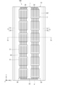
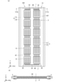
- FIG. 1 is a plan view showing an example of the external appearance of the solar cell module according to the first embodiment when viewed from above.
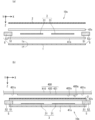
- FIG. 2 is a diagram showing an example of a hypothetical cross section of the solar cell module in FIG. 1 taken along line Ib-Ib.
- FIG. 3A is a diagram illustrating an example of the structure of the solar cell element when viewed from above on the first element surface.
- FIG. 3(b) is a diagram illustrating an example of the structure when the second element surface of the solar cell element is viewed from above.
- FIGS. 4A to 4C are diagrams each illustrating a cross-sectional state during manufacture in the first specific example of the method for manufacturing a solar cell module according to the first embodiment.
- FIGS. 9A and 9B are diagrams each illustrating a cross-sectional state during manufacture in the second specific example of the method for manufacturing a solar cell module according to the first embodiment.
- FIG. 6 is a diagram illustrating a state in which the solar cell module according to the first embodiment is bent.
- FIG. 7 is a diagram showing an example of a virtual cut surface of the solar cell module according to the second embodiment.
- FIG. 8 is an enlarged view of the area surrounded by the broken line in FIG. 7.
- FIGS. 9A and 9B are diagrams each illustrating a cross-sectional state during manufacture in the first specific example of the method for manufacturing a solar cell module according to the second embodiment.
- FIGS. 9A and 9B are diagrams each illustrating a cross-sectional state during manufacture in the first specific example of the method for manufacturing a solar cell module according to the second embodiment.
- FIGS. 9A and 9B are diagrams each illustrating a cross-sectional state during manufacture in the first specific example of the method for manufacturing a solar
- FIGS. 10A and 10B are diagrams each illustrating a cross-sectional state during manufacture in a second specific example of the method for manufacturing a solar cell module according to the second embodiment.
- FIG. 11 is a diagram showing an example of a virtual cut surface of the solar cell module according to the third embodiment.
- FIGS. 12(a) and 12(b) are diagrams each illustrating a cross-sectional state during manufacturing in the method for manufacturing a solar cell module according to the third embodiment.
- FIG. 13A is a plan view showing an example of the external appearance of the solar cell module according to the fourth embodiment when viewed from above.
- FIG. 13(b) is a diagram showing an example of a virtual cut surface of the solar cell module of FIG. 13(a) along line IIb-IIb.
- FIG. 14 is a plan view showing an example of the external appearance of the solar cell module according to the fifth embodiment when viewed from above.
- FIG. 15A is a plan view showing an example of the external appearance of the solar cell module according to the sixth embodiment when viewed from above.
- FIG. 15(b) is a diagram illustrating an example of a hypothetical cut plane along line IIIb-IIIb of the solar cell module of FIG. 15(a).
- FIG. 16A is a diagram illustrating an example of the structure of the solar cell module according to the seventh embodiment when viewed from above.
- FIG. 16(b) is a diagram showing an example of a hypothetical cut plane along line IVb-IVb of the solar cell module of FIG. 16(a).
- FIG. 17A is a diagram illustrating an example of the structure of the solar cell section according to the seventh embodiment when viewed from above.
- FIG. 17(b) is a diagram showing an example of a hypothetical cut plane along the Vb-Vb line of the solar cell portion of FIG. 17(a).
- the inventor has created a technology that improves the flexibility and strength of solar cell modules. Regarding this, the first to seventh embodiments will be described below based on the drawings.
- FIGS. 1 to 17(b) A right-handed XYZ coordinate system is attached to FIGS. 1 to 17(b).
- the short direction of the front surface 10f of the solar panel 10 is the +X direction
- the longitudinal direction of the front surface 10f is the +Y direction
- the normal to the front surface 10f is orthogonal to both the +X direction and the +Y direction.
- the direction is the +Z direction.
- Solar cell module> A solar cell module 100 according to a first embodiment will be described based on FIGS. 1 to 3(b).
- the solar cell module 100 includes, for example, a solar cell panel 10.
- the solar cell panel 10 has, for example, a light-receiving surface (also referred to as a front surface) 10f through which light mainly enters, and a back surface 10b located on the opposite side of the front surface 10f.
- the front surface 10f is in a state facing the +Z direction.
- the back surface 10b is in a state facing the -Z direction.
- the +Z direction is set, for example, in a direction facing the sun, which is in the south.
- the front surface 10f has a rectangular shape, which is an example of a rectangular shape.
- the solar cell module 100 may further include a terminal box (not shown) for extracting the power generated by the solar cell panel 10 to the outside.
- the solar cell panel 10 includes, for example, a surface protective layer 1, a back surface protective layer 2, a solar cell section 3, a filler 4, and a support member 5. There is.
- the surface protection layer 1 has, for example, a first surface 1f and a second surface 1s (see FIG. 2).
- the first surface 1f constitutes, for example, the front surface 10f of the solar cell panel 10. That is, the surface protective layer 1 has a rectangular shape, which is an example of a rectangular shape.
- the first surface 1f is exposed to a space (also referred to as external space) 200 outside the solar cell module 100.
- the second surface 1s is a surface opposite to the first surface 1f.
- the surface protective layer 1 has, for example, translucency. Specifically, the surface protection layer 1 has, for example, transparency to light having a wavelength in a specific range.
- the specific range of wavelengths includes, for example, the wavelength of light that can be photoelectrically converted by the solar cell unit 3. If the wavelengths in the specific range include wavelengths of sunlight with high irradiation intensity, the photoelectric conversion efficiency of the solar cell module 100 can be improved.
- the surface protective layer 1 As the material of the surface protective layer 1, for example, a resin having weather resistance is applied.
- the surface protective layer 1 is made of, for example, a weather-resistant resin.
- weather resistance refers to a property that does not easily cause alterations such as deformation, discoloration, and deterioration when used outdoors, for example.
- the surface protection layer 1 reduces the intrusion of water such as water droplets from the external space 200 of the solar cell module 100 toward the solar cell section 3, and It has a property that allows moisture to easily pass from the filler 4 toward the external space 200 (also referred to as moisture-permeable waterproof property).
- the weather-resistant resin includes, for example, a fluorine-based resin.
- Fluorine-based resins include, for example, fluorinated ethylene propylene copolymer (FEP), ethylene tetrafluoroethylene copolymer (ETFE), and ethylene chlorotrifluoroethylene copolymer (Ethylene Chlorotrifluoroethylene). :ECTFE) etc.
- the surface protection layer 1 may be composed of two or more layers of resin having weather resistance.
- the fluorine-based resin applied to the surface protective layer 1 may be, for example, two or more types of resin. For this reason, for example, a mode is conceivable in which the fluororesin applied to the surface protective layer 1 includes at least one resin among FEP, ETFE, and ECTFE.
- the thickness of the surface protective layer 1 is, for example, about 0.05 millimeter (mm) to 0.5 mm.
- the surface protective layer 1 is made of a moisture permeable resin with a relatively low density and is thin, so the surface protective layer 1 is light. For this reason, the weight of the solar cell module 100 can be reduced compared to, for example, a structure in which high-density glass having a thickness of about 1 mm or more is used instead of the surface protective layer 1. can be made into a thin film.
- the material for the surface protective layer 1 resins such as acrylic resin and polycarbonate can be used instead of or together with the fluorine resin.
- the thickness of the resin is, for example, about 0.03 mm to 0.6 mm.
- the surface protection layer 1 may be formed by laminating multiple types of resins.
- the solar cell section 3 is located, for example, between the front surface protective layer 1 and the back surface protective layer 2. In other words, the solar cell section 3 is in a state opposite to the front surface protective layer 1 in the Z direction, and is also in a state opposite to the back surface protective layer 2 in the Z direction.
- the solar cell section 3 includes, for example, a plurality of solar cell elements 31.
- the plurality of solar cell elements 31 are located between the second surface 1s of the surface protection layer 1 and the back surface protection layer 2.
- the plurality of solar cell elements 31 are two-dimensionally arranged. In the examples shown in FIGS. 1 and 2, the plurality of solar cell elements 31 are arranged in a plane so as to be located along the second surface 1s of the surface protective layer 1. Note that the plurality of solar cell elements 31 may be arranged one-dimensionally.
- the solar cell section 3 further includes, for example, a plurality of first wiring members 32, a second wiring member 33, and a third wiring member 34.
- the solar cell section 3 includes, for example, a plurality of (here, two) solar cell strings 30.
- the plurality of solar cell strings 30 are arranged in the X direction.
- Each of the plurality of solar cell strings 30 includes, for example, a plurality of (here, five) solar cell elements 31 and a plurality of first wiring members 32.
- the plurality of solar cell elements 31 are arranged in the Y direction, for example.
- the plurality of first wiring members 32 are in a state of electrically connecting two mutually adjacent solar cell elements 31 among the plurality of solar cell elements 31.
- the second wiring member 33 is in a state of electrically connecting two mutually adjacent solar cell strings 30 among the plurality of solar cell strings 30 .
- two third wiring members 34 are connected to two solar cell strings 30, respectively.
- a third wiring material 34 connected to the solar cell string 30 located at the end in the -X direction and a third wiring material connected to the solar cell string 30 located at the end in the +X direction most. 34 is in a state of being pulled out to the outside of the solar cell panel 10.
- Each of the plurality of solar cell elements 31 can convert light energy into electrical energy.
- Each of the plurality of solar cell elements 31 has a surface (also referred to as a first element surface) 31f located on the front surface side and a surface (second element surface) opposite to this first element surface 31f. (also referred to as a surface) 31s.
- the first element surface 31f is in a state facing the +Z direction
- the second element surface 31s is in a state facing the -Z direction.
- the first element surface 31f primarily serves as a surface onto which light is incident (also referred to as a light-receiving surface), and the second element surface 31s primarily serves as a surface onto which light does not enter (also referred to as a non-light-receiving surface). ).
- each of the plurality of solar cell elements 31 includes a semiconductor substrate 310, a first output extraction electrode 311, and a first current collector. It has an electrode 312, a second output extraction electrode 313, and a second current collection electrode 314.
- the semiconductor substrate 310 includes, for example, a crystalline semiconductor such as crystalline silicon, an amorphous semiconductor such as amorphous silicon, four types of elements such as copper, indium, gallium, and selenium, or two types of elements such as cadmium and tellurium. Compound semiconductors using Here, it is assumed that crystalline silicon is applied to the semiconductor substrate 310.
- the semiconductor substrate 310 mainly includes a region having a first conductivity type (also referred to as a first conductivity type region) and a region having a second conductivity type opposite to the first conductivity type (a second conductivity type region). ).
- the first conductivity type region is located, for example, on the second element surface 31s side of the semiconductor substrate 310 in the ⁇ Z direction.
- the second conductivity type region is located, for example, in the surface layer portion of the semiconductor substrate 310 on the first element surface 31f side in the +Z direction.
- the semiconductor substrate 310 has a pn junction located at the interface between the first conductivity type region and the second conductivity type region.
- the thickness of the semiconductor substrate 310 is, for example, approximately 0.15 mm to 0.5 mm.
- the first output extraction electrode 311 and the first current collection electrode 312 are located, for example, on the surface of the semiconductor substrate 310 on the first element surface 31f side.
- a bus bar electrode is applied to the first output extraction electrode 311.
- a finger electrode is applied to the first current collecting electrode 312.
- five substantially parallel first output extraction electrodes 311 are located on the first element surface 31f side of the semiconductor substrate 310, and a large number of substantially parallel first current collecting electrodes 312 are located on the first element surface 31f side of the semiconductor substrate 310. , are positioned substantially perpendicular to the five first output extraction electrodes 311.
- FIG. 3A five substantially parallel first output extraction electrodes 311 are located on the first element surface 31f side of the semiconductor substrate 310, and a large number of substantially parallel first current collecting electrodes 312 are located on the first element surface 31f side of the semiconductor substrate 310. , are positioned substantially perpendicular to the five first output extraction electrodes 311.
- FIG. 3A five substantially parallel first output extraction electrodes 311
- each of the first output extraction electrodes 311 has a long shape in the Y direction, and each of the first current collecting electrodes 312 has a linear shape long in the X direction. have. Furthermore, a region on the second conductivity type region of the semiconductor substrate 310 where the first output extraction electrode 311 and the first current collecting electrode 312 are not formed is made of, for example, silicon nitride. An insulating film may be provided as a certain anti-reflection film 315.
- the main component of the first output extraction electrode 311 is silver
- the first output extraction electrode 311 is formed by applying silver paste into a desired shape by screen printing or the like and then firing it. can be formed.
- main component refers to a component that has the largest (highest) ratio (also referred to as content) among the contained components.
- a metal paste containing a metal powder containing silver as a main component, an organic vehicle, and a glass frit is applied to the silver paste.
- the first current collecting electrode 312 is silver
- the first current collecting electrode 312, like the first output extraction electrode 311 is made by applying silver paste into a desired shape by screen printing or the like. It can be formed by later firing.
- the first output extraction electrode 311 and the first current collection electrode 312 may be formed in separate processes, or may be formed in the same process.
- the second output extraction electrode 313 and the second current collection electrode 314 are located, for example, on the surface of the semiconductor substrate 310 on the second element surface 31s side.
- a bus bar electrode is applied to the second output extraction electrode 313.
- five rows of second output extraction electrodes 313 that are substantially parallel to each other along the +Y direction are located on the second element surface 31s side of the semiconductor substrate 310.
- the second current collecting electrode 314 is located on the second element surface 31s side of the semiconductor substrate 310, except for a portion where the second output extraction electrode 313 and the second current collecting electrode 314 are overlapped and connected to each other. It is located almost on the entire area where the two-output extraction electrode 313 is not formed.
- Each of the five rows of second output extraction electrodes 313 includes, for example, four electrodes arranged in a row. Further, for example, a passivation film is formed between the first conductivity type region of the semiconductor substrate 310 and the second output extraction electrode 313 and the second current collecting electrode 314 by forming a thin film of oxide or nitride such as aluminum oxide in a desired pattern. may exist as .
- the main component of the second output extraction electrode 313 is silver
- the second output extraction electrode 313, like the first output extraction electrode 311 can be formed by applying silver paste into the desired shape by screen printing or the like. It can be formed by being fired after being applied.
- the second current collecting electrode 314 may be formed by applying aluminum paste into a desired shape by screen printing or the like and then firing it.
- aluminum paste containing a metal powder containing aluminum as a main component, an organic vehicle, and a glass frit is applied to the aluminum paste.
- the first wiring material 32 connects, for example, a first output extraction electrode 311 of one solar cell element 31 and a second output extraction electrode 313 of another solar cell element 31 adjacent to this one solar cell element 31. are electrically connected.
- the outer edges of the plurality of first wiring members 32 attached to each of the solar cell elements 31 are virtually drawn with two-dot chain lines.
- the first wiring member 32 has an elongated shape that is long in the Y direction.
- the first wiring material 32 is in a state of being joined to the first output extraction electrode 311 and the second output extraction electrode 313, for example.
- a portion (a first (also referred to as a joint portion) 321 exists. Therefore, for example, the first wiring material 32 is in a state of being joined to the first output extraction electrode 311 of one solar cell element 31 via the first joint portion 321. Also, for example, a portion located between the first wiring material 32 and the second output extraction electrode 313 and joining the first wiring material 32 and the second output extraction electrode 313 (also referred to as a second joint portion) 322 exists. Therefore, for example, the first wiring material 32 is in a state where it is joined to the second output extraction electrode 313 of another solar cell element 31 adjacent to one solar cell element 31 via the second joint portion 322. It is in.
- the first wiring material 32 for example, a linear or band-shaped electrically conductive metal body is applied.
- a low melting point alloy such as solder or a low melting point single metal is applied. More specifically, for example, a copper foil having a thickness of about 0.1 mm to 0.2 mm and a width of about 1 mm to 2 mm is applied to the first wiring material 32, and solder is applied to the entire surface of the first wiring material 32. is covered.
- the first wiring material 32 is in a state of being electrically connected to the first output extraction electrode 311 and the second output extraction electrode 313, for example, by soldering.
- the solder located between the first wiring material 32 and the first output extraction electrode 311 constitutes the first joint portion 321. Further, for example, the solder located between the first wiring material 32 and the second output extraction electrode 313 constitutes the second joint portion 322 .
- the filler 4 is in a state covering the solar cell part 3 between the front protection layer 1 and the back protection layer 2. In other words, the filler 4 is in a state covering the plurality of solar cell elements 31 between the front protective layer 1 and the back protective layer 2. From another point of view, the filler 4 is filled in, for example, a region (also referred to as a gap region) 10g between the surface protective layer 1 and the back surface protective layer 2 while covering the solar cell section 3. be.
- the filler 4 has a first surface 4f located on the front surface, and a second surface 4s located on the opposite side to the first surface 4f.
- the first surface 4f of the filler 4 is in contact with the second surface 1s of the surface protection layer 1, and the second surface 4s of the filler 4 is in contact with the back surface protection layer 2.
- the filler 4 includes, for example, a filler (also referred to as a first filler) 41 located on the front surface 10f side and a filler (also referred to as a second filler) located on the back surface 10b side. 42).
- the first filler 41 is in a state of forming, for example, the first surface 4f, and is in a state of covering the entire surface of the solar cell section 3 on the surface protection layer 1 side. In other words, the first filler 41 is in a state of covering the plurality of solar cell elements 31, for example, between the surface protection layer 1 and the plurality of solar cell elements 31.
- the second filler 42 is in a state of forming, for example, the second surface 4s, and is in a state of covering the entire surface of the solar cell section 3 on the back surface protective layer 2 side.
- the second filler 42 is in a state of covering the plurality of solar cell elements 31, for example, between the back surface protective layer 2 and the plurality of solar cell elements 31. Therefore, in the first embodiment, the solar cell section 3 is in a state of being sandwiched and surrounded by the first filler 41 and the second filler 42, for example. Thereby, for example, the attitude of the solar cell section 3 can be maintained by the filler 4.
- the filler 4 has, for example, translucency.
- the filler 4 has, for example, translucency to light having a wavelength in the above-mentioned specific range.
- the incident light from the front surface 10f side can reach up to the solar cell section 3.
- the material for the first filler 41 for example, ethylene vinyl acetate copolymer (EVA), polyvinyl acetal such as polyvinyl butyral (PVB), acid-modified resin, etc. are used.
- EVA ethylene vinyl acetate copolymer
- PVB polyvinyl acetal
- acid-modified resin etc.
- the acid-modified resin includes, for example, a modified polyolefin resin that can be formed by graft modification of a resin such as polyolefin with an acid.
- acids that can be used for graft modification of acid-modified resins include acrylic acid, methacrylic acid, maleic acid, fumaric acid, itaconic acid, maleic anhydride, hymic anhydride, itaconic anhydride, and citraconic anhydride.
- Ru As the material for the second filler 42, for example, like the first filler 41, polyvinyl acetal such as EVA and PVB, acid-modified resin, etc. are used.
- the first filler 41 and the second filler 42 may be made of two or more types of materials, for example.
- the second filler 42 may contain, for example, a pigment.
- a white pigment included, the light transmitted through the solar cell section 3 can be reflected by the second filler 42 and made to enter the solar cell section 3 again. Thereby, the power generation efficiency of the solar cell module 100 can be improved.
- the filler 4 may not include the second filler 42 and may include only the first filler 41.
- the first filler 41 covers the solar cell section 3 between the front protective layer 1 and the back protective layer 2.
- the back surface protective layer 2 is in a state of forming the back surface 10b of the solar cell panel 10, for example.
- the back surface protective layer 2 is in a state facing the second surface 1s of the surface protective layer 1.
- the back surface protective layer 2 is in contact with the filler 4 on the side opposite to the surface protective layer 1 with respect to the filler 4 .
- the back surface protective layer 2 is located facing the solar cell portion 3 and the inner portion 51 of the support member 5 in the Z direction.
- the inner portion 51 is a portion of the support member 5 on the solar cell section 3 side with respect to the outer portion 52 in the X direction.
- the back surface protective layer 2 can, for example, protect the solar cell section 3 from the back surface 10b side.
- a back sheet forming the back surface 10b is applied to the back surface protective layer 2.
- the thickness of the back sheet is, for example, about 0.15 mm to 0.5 mm.
- resin is used as the material for the back sheet.
- the same material as the surface protective layer 1 can be applied to the resin.
- the back surface protective layer 2 has the same or similar shape to the surface protective layer 1 when viewed in plan from the back surface 10b side. For example, a configuration is assumed in which both the surface protective layer 1 and the back surface protective layer 2 have a rectangular outer shape when viewed from the back surface 10b side.
- the support member 5 is a member for improving the rigidity of the solar cell panel 10, and has higher rigidity than all of the surface protection layer 1, back surface protection layer 2, and filler 4, for example.
- metal can be used as the material of the support member 5, and as a more specific example, aluminum or stainless steel can be used.
- the support member 5 is located adjacent to the solar cell section 3 with an interval when viewed from above toward the main surface of the surface protection layer 1. In other words, the support member 5 is located adjacent to the solar cell section 3 with an interval when viewed with the line of sight along the Z direction. Hereinafter, viewing with the line of sight along the Z direction will also simply be referred to as planar viewing.
- the support member 5 includes an inner portion 51 and an outer portion 52, and the inner portion 51 is located between the front protective layer 1 and the back protective layer 2 and covered with the filler 4. There is. In other words, the inner portion 51 is in a state opposite to the front surface protective layer 1 in the Z direction, is in a state opposite to the back surface protective layer 2 in the Z direction, and is in a state covered by the filler 4.
- the outer portion 52 extends from the inner portion 51 to the side opposite to the solar cell portion 3 (that is, to the outside), and is not covered with the filler 4, for example.
- the outer portion 52 extends from the inner portion 51 to the outside of the front protective layer 1 and the back protective layer 2 in plan view. That is, the outer portion 52 is in a state where it is not facing the front surface protective layer 1 in the Z direction, and is also not facing the back surface protective layer 2 in the Z direction.
- the inner portion 51 of the support member 5 is located on the solar cell section 3 side (that is, inside) with respect to the outer portion 52 of the support member 5 in plan view.
- the support member 5 has a plate-like shape, and has a rectangular shape in plan view.
- the ZX cross section of the support member 5 also has a rectangular shape.
- the corners of the support member 5 may be chamfered as appropriate.
- the longitudinal direction (here, the Y direction) of the support member 5 is, for example, along one side of the surface protection layer 1. Further, the longitudinal direction of the support member 5 is, for example, along the arrangement direction (here, the Y direction) of the plurality of solar cell elements 31 included in one solar cell string 30. That is, the longitudinal direction of the support member 5 is along, for example, the longitudinal direction of the first wiring member 32 (here, the Y direction).
- the solar panel 10 includes two support members 5.
- the two support members 5 are located along both sides of the surface protection layer 1 on both sides in the X direction.
- the two sides located on both sides of the X direction herein refer to one side of the surface protective layer 1 extending along the Y direction at the end in the -X direction, and one side extending along the Y direction at the end in the +X direction. and one extending side. That is, one support member 5 is located at the end of the surface protection layer 1 in the -X direction and has a rectangular shape with the longitudinal direction being the Y direction, and the other support member 5 is located at the end of the surface protection layer 1 in the -X direction. 1, and has a rectangular shape whose longitudinal direction is the Y direction.
- the length of the support member 5 in the longitudinal direction is, for example, approximately equal to the length of the surface protection layer 1.
- the width of the support member 5 in the transverse direction (here, the X direction) is set to, for example, several tens of mm or more.
- the width of the inner portion 51 of the support member 5 is set to, for example, approximately 20% or more and 80% or less of the width of the support member 5.
- the thickness of the support member 5 is larger than the thickness of the solar cell section 3, and is set to about 1 mm to 5 mm, for example.
- the outer portion 52 of the support member 5 is attached to an attachment target member such as an external building material.
- outer portion 52 may be formed with mounting holes (not shown).
- the mounting hole passes through the outer portion 52 in the Z direction.
- the solar cell panel 10 can be attached to the attachment target member by passing the mounting bolt through the attachment hole and screwing into the attachment target member.
- the two support members 5 are located on both sides of the solar panel 10, so it is possible to fix the two support members 5 on both sides of the solar panel 10 to the attachment target member. can. Therefore, the solar cell panel 10 can be more firmly attached to the attachment target member. It can also be said that the support member 5 is a mounting member.
- the support members 5, which are rigid bodies, are not mainly located on both sides of the solar cell panel 10 in the Y direction. That is, the support member 5 is not substantially located at the end of the solar cell panel 10 in the +Y direction and extends along the X direction, but is located at the end of the solar cell panel 10 in the -Y direction. It is not substantially located at the end portion extending along the X direction either. Therefore, as shown in FIG. 6, by applying the external force F1 to the support member 5, the solar cell panel 10 can be bent in an arc shape when viewed in the direction along the Y direction. In other words, the solar cell panel 10 can be bent in an arc shape when viewed with the line of sight along the Y direction. For example, the solar cell panel 10 can be bent to a state along an arc with a radius of about several hundred mm (for example, 500 mm). According to this, it is easy to attach the solar cell panel 10 to the curved attachment target member.
- the distance between the front protective layer 1 and the back protective layer 2 is small in the solar cell section 3, and the distance between the solar cell section 3 and the support member 5 is small. Large in size. In other words, the distance (maximum value) between the front protective layer 1 and the back protective layer 2 between the solar cell section 3 and the support member 5 is the same as the distance between the front protective layer 1 and the back protective layer 2 in the solar cell section 3. (maximum value).
- the portion 4a referred to here is a portion of the filler 4 that is located between the solar cell section 3 and the support member 5 and is located continuously from the surface protective layer 1 to the back surface protective layer 2. .
- the thickness W1 of the portion 4a at the end on the support member 5 side is larger than the thickness W2 of the portion 4a at the end on the solar cell section 3 side.
- the difference between the thickness W1 and the thickness W2 may be, for example, 0.1 mm or more, 0.5 mm or more, or 1 mm or more.
- the thickness of the portion 4a of the filler 4 is, for example, in at least a partial region R1 between the support member 5 and the solar cell portion 3, from the solar cell portion 3 along the X direction. It gradually increases toward the support member 5. That is, the thickness of the portion 4a of the filler 4 increases monotonically in the region R1 from the solar cell portion 3 toward the support member 5 along the X direction. In other words, as the position in the X direction approaches the support member 5 from the solar cell section 3, the thickness of the portion 4a of the filler 4 at that position gradually increases. In short, the thickness of the portion 4a gradually increases in the region R1 toward the outside along the X direction.
- the amount of increase in the thickness of the entire region R1 may be, for example, 0.1 mm or more, 0.5 mm or more, or 1 mm or more.
- the shape of the portion 4a of the filler 4 is, for example, uniform in the Y direction.
- the first surface 4f and the second surface 4s of the filler 4 have shapes that are line symmetrical to each other with respect to the XY plane, but the drawing is shown schematically. However, it is not necessarily limited to this.
- the inner portion 51 of the support member 5, which is a rigid body, is covered with the filler 4 between the front protection layer 1 and the back protection layer 2. Therefore, the rigidity of the solar cell panel 10 can be improved.
- the support member 5 is located at the end of the solar cell panel 10 in the X direction and between both ends of the solar cell panel 10 in the Y direction, so that the rigidity in the Y direction is particularly improved. be able to.
- the support members 5 are not substantially located on both sides of the solar cell panel 10 in the Y direction. That is, the support member 5 is not substantially located at the end of the solar cell panel 10 in the +Y direction and extends along the X direction, but is located at the end of the solar cell panel 10 in the -Y direction. It is not substantially located at the end portion extending along the X direction either. Therefore, when viewed with the line of sight along the Y direction, the solar cell panel 10 can be bent in an arc shape (see FIG. 6). In such a bent state, a relatively large stress is generated in the portion of the solar cell panel 10 between the support member 5 and the solar cell section 3. More specifically, a large stress is generated in a portion of the solar cell panel 10 near the inner end surface 5a of the support member 5.
- the inner end surface 5a here is the end surface of the support member 5 on the solar cell section 3 side.
- the thickness of the filler 4 is large between the support member 5 and the solar cell part 3 and is small in the solar cell part 3.
- the thickness W1 is larger than the thickness W3. Therefore, the strength of the solar cell panel 10 can be improved between the support member 5 and the solar cell section 3. Therefore, the solar cell panel 10 can appropriately cope with stress due to bending.
- the filler 4 is thin in the solar cell section 3, the flexibility of the solar cell panel 10 can be improved. In other words, it is possible to achieve both flexibility and strength of the solar cell panel 10.
- the volume of the filler 4 can be made smaller compared to a structure in which the thickness W3 is increased to the same extent as the thickness W1, the material cost of the filler 4 can also be reduced.
- the thickness W1 of the portion 4a of the filler 4 is larger than the thickness W2, the strength of the solar cell panel 10 can be improved near the inner end surface 5a of the support member 5. Therefore, the solar cell panel 10 can more appropriately cope with the stress caused by the bending. Further, in the region R1, if the thickness of the portion 4a gradually increases from the solar cell portion 3 toward the support member 5, stress in the portion 4a can be effectively dispersed.
- the surface protective layer 1 is prepared.
- a resin film having rectangular front and back surfaces and weather resistance is prepared as the surface protection layer 1.
- a fluorine-based resin is used as the weather-resistant resin.
- the fluorine-based resin for example, FEP, ETFE, or ECTFE is used.
- the second surface 1s which is one surface of the surface protective layer 1, is subjected to a treatment for activating the surface, such as corona treatment or plasma treatment. Thereby, the adhesion between the surface protection layer 1 and the filler 4 can be improved in the lamination process described below.
- the surface protective layer 1 the sheet 41s, the sheet 41t, the solar cell part 3, the support member 5, the sheet 42s, the sheet 42t, and the back surface protection
- a stacked body 10s is formed.
- the solar cell section 3 is located between two support members 5, and these are arranged in a spaced-apart manner in the X direction. Further, at this time, wiring is appropriately positioned to be drawn out from the solar cell section 3 to the outside of the solar cell panel 10 and connected to a terminal box or the like.
- the plurality of solar cell elements 31 of the solar cell section 3 are connected to each other by a first wiring material 32 and a second wiring material 33. Further, the third wiring member 34 is connected to the solar cell section 3 .
- the sheet 41s and the sheet 41t are sheets made of resin (such as EVA) that is the base material of the first filler 41.
- the sheet 41s is located between the surface protection layer 1 and the solar cell section 3 and between the surface protection layer 1 and the support member 5. That is, the sheet 41s is located on the surface protection layer 1, and the solar cell section 3 and the support member 5 are located on the sheet 41s.
- the sheet 41s has a rectangular shape as an example of a rectangular shape in plan view.
- the sheet 41t is located between the support member 5 and the solar cell section 3 and above the sheet 41s.
- two support members 5 are located, so two sheets 41t are located.
- each sheet 41t has, for example, an elongated shape that is long in the Y direction.
- the width of each sheet 41t is narrower than the distance between the support member 5 and the solar cell section 3. That is, in the examples of FIGS. 4(b) and 4(c), the sheet 41t is located in a state where it does not face both the support member 5 and the solar cell section 3 in the Z direction.
- the sheet 42s and the sheet 42t are sheets made of resin (such as EVA) that is the base material of the second filler 42.
- the sheet 42s and the sheet 42t may contain pigment.
- the sheet 42s is located between the back protection layer 2 and the solar cell section 3 and between the back protection layer 2 and the support member 5. In other words, the sheet 42s is positioned with both ends facing the support member 5, respectively.
- the sheet 42s has a rectangular shape as an example of a rectangular shape in plan view.
- the sheet 42t is located between the support member 5 and the solar cell section 3 and above the sheet 42s.
- two support members 5 are located, so two sheets 42t are located.
- each sheet 42t has, for example, an elongated shape that is long in the Y direction.
- the width of each sheet 42t is narrower than the distance between the support member 5 and the solar cell section 3. That is, in the examples shown in FIGS. 4(b) and 4(c), the sheet 42t is positioned so as not to face both the support member 5 and the solar cell section 3 in the Z direction.
- the back surface protective layer 2 is located on the sheet 42s and the sheet 42t.
- the sheet 41t and the sheet 42t are located between the support member 5 and the solar cell section 3 in plan view. Therefore, the total thickness of the sheet between the support member 5 and the solar cell section 3 is larger than the total thickness of the sheet in the region facing the solar cell section 3 by the amount of the sheet 41t and the sheet 42t.
- the sheet 42s and the back protective layer 2 are shown in a flat plate shape, if they are flexible or pliable, the central part of the sheet 42s and the back protective layer 2 will be the surface protective layer. It can bend to one side.
- a lamination process is performed on the laminate 10s.
- a laminate device (laminator) is used to integrate the laminate 10s.
- the laminate 10s is placed on a heater board in a chamber, and while the pressure inside the chamber is reduced from 50 Pascals (Pa) to about 150 Pa, the laminate 10s is heated from 100 degrees Celsius (100 degrees Celsius) to 200 degrees Celsius. Heat to about 200°C.
- the sheets 41s, 41t, 42s, and 42t become fluidized to some extent by heating.
- the laminate 10s is pressed in the Z direction with a pressing member such as a diaphragm sheet, thereby integrating the laminate 10s.
- the sheet 41t and the sheet 42t are located in the laminate 10s.
- the total thickness of the sheet increases between the support member 5 and the solar cell section 3. Therefore, the thickness of the filler 4 between the support member 5 and the solar cell section 3 can be increased more easily.
- the sheets 41t and 42t are located, a gap due to the difference in thickness between the support member 5 and the solar cell element 31 will be created between the support member 5 and the solar cell part 3 of the laminate 10s. can be reduced.
- the pressing body of the laminator can press the laminate 10s with sufficient pressure even between the support member 5 and the solar cell section 3.
- unevenness in pressure distribution caused by the difference in thickness between the support member 5 and the solar cell element 31 can be reduced. Therefore, the molten sheet is pressed against the surface protection layer 1, the support member 5, the solar cell section 3, and the back surface protection layer 2 with sufficient pressure even between the support member 5 and the solar cell section 3.
- the filler 4 can be bonded to these with higher adhesive strength.
- the sheet 42t is located above the sheet 42s in the lamination process, but it may be located between the sheet 42s and the sheet 41t.
- the sheet 41t is located on the sheet 41s, it may be located between the sheet 41s and the surface protection layer 1.
- a plurality of sheets 41t may be stacked in the Z direction, or a plurality of sheets 42t may be stacked in the Z direction. Further, only one of the sheet 41t and the sheet 42t may be located.
- the sheet 41s and the sheet 41t are separate sheets in the above example, they may be integrated. That is, the thickness of the sheet in the region between the support member 5 and the solar cell section 3 only needs to be larger than the thickness of the sheet in the region facing the solar cell section 3. The same applies to the sheet 42s and the sheet 42t.
- a terminal box or the like may be attached to the solar cell panel 10 as appropriate.
- wiring drawn out from the solar cell section 3 to the outside of the solar cell panel 10 is appropriately connected to a terminal in the terminal box. Thereby, the solar cell module 100 is assembled.
- the solar cell panel 10 including the support member 5 is integrated by lamination processing. Therefore, the solar cell panel 10 is easier to assemble than a structure in which an external frame (not shown) is attached to the solar cell panel 10 with screws or the like instead of the support member 5.
- the sheets 41t and 42t may not be located in the laminate 10s.
- the pressing surface 400s of the pressing body 400 of the laminator may have a stepped shape.
- the pressing surface 400s is a surface that contacts the laminate 10s and presses the laminate 10s.
- the pressing body 400 includes a diaphragm sheet 410, a first release sheet 420, and a second release sheet 421.
- the material of the diaphragm sheet 410 is, for example, an elastic member such as silicone rubber that is easily elastically deformable.
- the diaphragm sheet 410 is wider than the stacked body 10s in plan view, and is positioned facing the entire stacked body 10s.
- the first release sheet 420 is a sheet that has release properties.
- the first release sheet 420 is obtained, for example, by forming a release film such as a silicone coating on the surface of a sheet-like base material.
- the first release sheet 420 is located on the laminate 10s side with respect to the diaphragm sheet 410.
- the first release sheet 420 is positioned to overlap the diaphragm sheet 410.
- the first release sheet 420 is wider than the laminate 10s in plan view, and is positioned facing the entire laminate 10s.
- the second release sheet 421 is a sheet that has release properties.
- the second release sheet 421 is obtained, for example, by forming a release film such as a silicone coating on the surface of a sheet-like base material.
- the second release sheet 421 is located on the laminate 10s side with respect to the first release sheet 420.
- the second release sheet 421 is positioned to overlap the first release sheet 420.
- the second release sheet 421 has, for example, an elongated shape that is long in the Y direction in plan view.
- the width of the second release sheet 421 in the X direction is narrower than the interval between the two supporting members 5 and is greater than or equal to the width of the solar cell section 3 .
- the second release sheet 421 is in a state where it faces the laminate 10s in the Z direction between the two support members 5, and does not face the support member 5 in the Z direction. Further, the second release sheet 421 is in a state facing the entire solar cell section 3 in the Z direction.
- the length of the second release sheet 421 in the Y direction is, for example, longer than the length of the laminate 10s in the Y direction.
- the pressing surface 400s which is the surface of the pressing body 400 on the laminate 10s side, has a step on both sides of the second release sheet 421, and the second release sheet 421 of the pressing surface 400s The portion corresponding to the second release sheet 421 protrudes toward the laminate 10s by the thickness of the second release sheet 421.
- the pressing surface 400s includes a first region 401s facing the support member 5, and a second region 402s located closer to the laminate 10s than the first region 401s and corresponding to the solar cell section 3.
- the step between the first region 401s and the second region 402s is located between the support member 5 and the solar cell section 3 in the X direction.
- the pressing surface 400s of such a pressing body 400 has a stepped shape corresponding to the thickness distribution of the filler 4 illustrated in FIG. 2 .
- the pressing body 400 initially presses the back protective layer 2 in the second area (that is, the second release sheet 421) facing the solar cell part 3, and then presses the back protective layer 2 in the second area facing the solar cell part 3 (that is, the second release sheet 421), and then Press the back protective layer 2 in one area. Therefore, the molten sheet easily flows toward the support member 5 and flows between the support member 5 and the solar cell section 3. Therefore, the thickness of the filler 4 between the support member 5 and the solar cell section 3 can be easily increased.
- the pressing body 400 has a more uniform pressure distribution.
- the laminated body 10s can be pressed with. As a result, even between the support member 5 and the solar cell part 3, the filler 4 adheres to the surface protection layer 1, the support member 5, the solar cell part 3, and the back protection layer 2 with higher adhesive strength. be able to.
- the thickness W1 of the filler 4 between the support member 5 and the solar cell section 3 is larger than the thickness W3 of the filler 4 between the solar cell elements 31, for example. Therefore, the strength of the solar cell panel 10 can be increased between the support member 5 and the solar cell section 3. As a result, the solar cell panel 10 can withstand the stress applied to the portion between the support member 5 and the solar cell section 3 due to the deflection due to the external force F1. Moreover, since the thickness W3 is small, the flexibility of the solar cell panel 10 can be improved.
- the number of solar cell elements 31 arranged in the X direction is 2, which is an even number.
- the number of solar cell elements 31 arranged in the direction orthogonal to the longitudinal direction of the support member 5 is an even number.
- the widths of each solar cell element 31 in the X direction are substantially equal to each other. Therefore, the solar cell element 31 does not exist at the center of the solar cell panel 10 in the X direction. That is, the center of the solar cell panel 10 corresponds to the portion between the solar cell elements 31.
- the solar cell panel 10 when the solar cell panel 10 is bent by the external force F1 (see also FIG. 6), a relatively large stress is also applied to the center of the solar cell panel 10 in the X direction. Further, even when a load such as snow is applied to the solar cell panel 10 while the support member 5 is attached to the attachment target member, the solar cell panel 10 can bend in an arc shape when viewed in the Y direction. Even in such a case, a relatively large stress is applied to the center of the solar cell panel 10 in the X direction.
- no solar cell element 31 is present at the center of the solar cell panel 10. Therefore, even when the solar cell panel 10 is bent due to the external force F1 or a load such as snow accumulation being applied to the solar cell panel 10, the stress applied to each solar cell element 31 is relatively small. Therefore, it is possible to reduce the possibility that problems such as performance deterioration of the solar cell element 31 due to stress will occur.
- the portion 4b of the filler 4 between the support member 5 and the surface protection layer 1 (corresponding to the first portion) is as follows. (corresponding to a predetermined first thickness distribution).
- the first thickness distribution is a thickness distribution in which the thickness W4 at the end of the portion 4b on the solar cell section 3 side is larger than the thickness W5 at the end of the portion 4b on the outer portion 52 side.
- the difference between the thickness W4 and the thickness W5 may be, for example, 0.01 mm or more, 0.05 mm or more, or 0.1 mm or more.
- the thickness of the portion 4b of the filler 4 gradually increases from the inner end surface 5a toward the outer end surface 5b at least in region R2 of the region facing the support member 5 in the Z direction. It may be reduced to
- the outer end surface 5b here is the end surface of the support member 5 on the opposite side to the solar cell section 3 in the X direction. It can also be said that the thickness of the portion 4b may decrease monotonically from the inner end surface 5a toward the outer end surface 5b in the region R2.
- the amount of reduction in thickness in the entire area R2 may be, for example, 0.01 mm or more, 0.05 mm or more, or 0.1 mm or more.
- the thickness of the portion 4a of the filler 4 gradually increases from the solar cell section 3 toward the support member 5, and the thickness of the portion 4b of the filler 4 increases from the inner end surface 5a to the outer end surface. It gradually decreases toward 5b. Therefore, the first surface 4f of the filler 4 has a convex shape that bulges in the +Z direction near the inner end surface 5a of the support member 5. Specifically, the first surface 4f is, for example, bulged in a smooth mountain shape.
- the shapes of the portions 4a and 4b of the filler 4 are uniform in the Y direction, for example.
- a portion 4c of the filler 4 between the support member 5 and the back protective layer 2 also has a thickness distribution (second thickness) described below. distribution).
- the second thickness distribution is a thickness distribution in which the thickness W6 at the end of the portion 4c on the solar cell section 3 side is larger than the thickness W7 at the end of the portion 4c on the outer portion 52 side.
- the difference between the thickness W6 and the thickness W7 may be, for example, 0.01 mm or more, 0.05 mm or more, or 0.1 mm or more.
- the thickness of the portion 4c of the filler 4 gradually increases from the inner end surface 5a toward the outer end surface 5b at least in the region R3 of the region facing the support member 5 in the Z direction. May be reduced. In other words, the thickness of the portion 4c may decrease monotonically from the inner end surface 5a toward the outer end surface 5b in the region R3.
- the amount of reduction in the thickness of the entire region R3 may be, for example, 0.01 mm or more, 0.05 mm or more, or 0.1 mm or more.
- the second surface 4s of the filler 4 has a convex shape that bulges in the -Z direction near the inner end surface 5a of the support member 5. Specifically, the second surface 4s is, for example, bulged in a smooth mountain shape.
- the shape of the portion 4c of the filler 4 is, for example, uniform in the Y direction.
- the explanation will focus on the distance between the front protective layer 1 and the back protective layer 2. That is, the distance between the front protective layer 1 and the back protective layer 2 at the inner end surface 5a of the support member 5 is the same as the distance between the front protective layer 1 and the back protective layer 2 at the end of the front protective layer 1 in the X direction or the end of the back protective layer 2 in the X direction. The distance is wider than the distance between the protective layer 1 and the back surface protective layer 2. The distance between the front protective layer 1 and the back protective layer 2 is maximum near the inner end surface 5a of the support member 5.
- the description will focus on the thickness of the structure consisting of the filler 4 and the support member 5. That is, the thickness of the structure at the position of the inner end surface 5a of the support member 5 is larger than the thickness of the structure at the end of the front protective layer 1 in the X direction or the end of the back protective layer 2 in the X direction. . The thickness of the structure is maximum near the inner end surface 5a of the support member 5.
- the thickness W4 of the portion 4b of the filler 4 is larger than the thickness W5. Therefore, the thickness of the solar cell panel 10 near the inner end surface 5a of the support member 5 can be further increased, and the strength of the solar cell panel 10 near the inner end surface 5a can be further improved. Therefore, even if the external force F1 is increased and the solar cell panel 10 is deflected more, the solar cell panel 10 can withstand the stress. Further, since the thickness W5 of the filler 4 is smaller than the thickness W4, the material cost of the filler 4 can be reduced compared to a structure in which the thickness W5 of the filler 4 is increased to the same extent as the thickness W4.
- the thickness W6 of the portion 4c of the filler 4 is larger than the thickness W7. Therefore, the thickness of the solar cell panel 10 near the inner end surface 5a of the support member 5 can be further increased, and the strength of the solar cell panel 10 near the inner end surface 5a can be further improved. Therefore, even if the external force F1 is increased and the solar cell panel 10 is deflected more, the solar cell panel 10 can withstand the stress. Further, since the thickness W7 of the filler 4 is smaller than the thickness W6, the material cost of the filler 4 can be reduced compared to a structure in which the thickness W7 of the filler 4 is increased to the same extent as the thickness W6.
- first surface 4f and the second surface 4s of the filler 4 have shapes that are line symmetrical to each other with respect to the XY plane, but the drawings are not shown schematically. However, this is not necessarily the case.
- the thickness of either the portion 4b or the portion 4c of the filler 4 may be uniform.
- either the portion 4b or the portion 4c may have a flat plate shape with a uniform thickness. This is because if either the portion 4b or the portion 4c has the above-mentioned thickness distribution, the strength of the solar cell panel 10 can be improved in the vicinity of the inner end surface 5a.
- the surface protective layer 1 the sheet 41s, the sheet 41u, the solar cell part 3, the support member 5, the sheet 42s, the sheet 42u, and the back surface protective layer 2.
- a stacked body 10s is formed. That is, compared to the first specific example of the first embodiment, sheets 41u and 42u are used instead of sheets 41t and 42t, respectively.
- the sheet 41u is a sheet made of resin (such as EVA) that is a base material of a part of the first filler 41.
- the sheet 41u is located above the sheet 41s.
- each sheet 41u has, for example, an elongated shape that is long in the Y direction.
- the sheet 41u is located in a region spanning the inner end surface 5a of the support member 5 in the X direction.
- the outer part of the sheet 41u in the X direction is located between the surface protection layer 1 and the support member 5, and the inner part of the sheet 41u in the X direction is located inside the inner end surface 5a of the support member 5. ing.
- the inner portion of this sheet 41u is located, for example, in a state where it does not face the solar cell section 3 in the Z direction.
- the outer end of the sheet 41u in the X direction is located inside, for example, with respect to the end of the surface protective layer 1 and the end of the sheet 41s in the X direction.
- the sheet 42u is a sheet made of resin (such as EVA) that forms part of the second filler 42.
- the sheet 42u is located above the sheet 42s.
- two support members 5 are located, so two sheets 42u are located.
- each sheet 42u has, for example, an elongated shape that is long in the Y direction.
- the sheet 42u is located in a region spanning the inner end surface 5a of the support member 5 in the X direction. That is, the outer part of the sheet 42u in the X direction is located between the back protective layer 2 and the support member 5, and the inner part of the sheet 42u in the X direction is located inside the inner end surface 5a of the support member 5. ing.
- the inner portion of this sheet 42u is located, for example, in a state where it does not face the solar cell section 3 in the Z direction. Further, the outer end of the sheet 42u in the X direction is located inside, for example, with respect to the end of the back protective layer 2 and the end of the sheet 42s in the X direction.
- a lamination process is performed on the laminate 10s.
- a laminate device laminated to integrate the laminate 10s.
- the solar cell panel 10 shown in FIGS. 7 and 8 can be manufactured.
- the sheet 41u is positioned so as to straddle the inner end surface 5a of the support member 5. Therefore, the thickness W4 of the portion 4b of the filler 4 can be increased more easily. Further, in plan view, the outer end of the sheet 41u is located inside the end of the surface protective layer 1 and the end of the sheet 41s, so that the thickness W5 of the portion 4b can be more easily reduced than the thickness W4. be able to.
- the sheet 42u is positioned so as to straddle the inner end surface 5a of the support member 5. Therefore, the thickness W6 of the portion 4c of the filler 4 can be increased more easily. Further, in plan view, the outer end of the sheet 42u is located inside the end of the back protective layer 2 and the end of the sheet 41s, so that the thickness W7 of the portion 4c can be more easily reduced than the thickness W6. be able to.
- the sheet 41u and the sheet 42u may not be located in the laminate 10s.
- the pressing surface 400s of the pressing body 400 may have a stepped shape.
- the pressing body 400 further includes a third release sheet 422, compared to the pressing body 400 of FIG. 5(b).
- the third release sheet 422 is a sheet that has release properties.
- the third release sheet 422 is obtained, for example, by forming a release film such as a silicone coating on the surface of a sheet-like base material.
- the third release sheet 422 is located on the laminate 10s side with respect to the first release sheet 420.
- the third release sheet 422 is positioned to overlap the first release sheet 420.
- the third release sheet 422 has, for example, an elongated shape that is elongated in the Y direction, and is positioned to face the end of the back surface protective layer 2 in the X direction in the Z direction.
- An inner end 422a of the third release sheet 422 on the second release sheet 421 side is located between the end of the back protective layer 2 and the inner end surface 5a of the support member 5 in the X direction.
- An outer end 422b of the third release sheet 422 on the opposite side to the second release sheet 421 is located outside of the end of the back protective layer 2 in the X direction.
- the pressing surface 400s of the pressing body 400 has a concave shape that is recessed in a region facing the vicinity of the inner end surface 5a of the support member 5 in the Z direction. More specifically, the pressing surface 400s includes a first region 401s that faces the inner end surface 5a of the support member 5, and a second region that is located closer to the laminate 10s than the first region 401s and that faces the solar cell section 3. It has a region 402s and a third region 403s located closer to the stacked body 10s than the first region 401s and facing the end of the back surface protective layer 2.
- the pressing surface 400s of such a pressing body 400 has a stepped shape according to the thickness distribution of the filler 4 illustrated in FIGS. 7 and 8.
- such a pressing body 400 presses regions of the back protective layer 2 at both ends in the The back protective layer 2 is pressed. Therefore, the molten sheet flows from both sides in the X direction to the vicinity of each inner end surface 5a. As a result, the thickness of the filler 4 can be easily increased near the inner end surface 5a of the support member 5.
- the support surface of a support (not shown) that supports the surface protection layer 1 may have a stepped shape similar to the pressing surface 400s of the pressing body 400. That is, the support body may include the first release sheet 420, the second release sheet 421, and the third release sheet 422 of the press body 400 in an upside-down state.
- Solar cell module> In the first embodiment and the second embodiment, as shown in FIG. It may be located on the side.
- the end 1a can be said to be the end of the surface protection layer 1 on the support member 5 side
- the end 2a can be said to be the end of the back surface protection layer 2 on the support member 5 side.
- the -X direction end 2a of the back protective layer 2 is located on the solar cell part 3 side with respect to the -X direction end 1a of the front protective layer 1, and the +X
- the end 2a in the direction may be located on the solar cell section 3 side with respect to the end 1a of the surface protection layer 1 in the +X direction.
- the width of the back surface protective layer 2 in the X direction may be smaller than the width of the surface protective layer 1 in the X direction.
- an end 42a of the filler 4 on the back surface protective layer 2 side and the outer portion 52 side is connected to an end 41a of the filler 4 on the surface protective layer 1 side and the outer portion 52 side.
- it may be located on the solar cell section 3 side.
- the end 42a of the filler 4 in the -X direction and the -Z direction is located on the solar cell section 3 side with respect to the end 41a of the filler 4 in the -X direction and the +Z direction.
- the +X direction and -Z direction end 42a of the filling material 4 may be located on the solar cell part 3 side with respect to the +X direction and +Z direction end 41a of the filling material 4.
- the back protection layer 2 may be located avoiding the area facing each support member 5 in the Z direction, and the filler 4 may be located on each support member 5. It may be located in the -Z direction (that is, on the opposite side to the surface protection layer 1) and away from the region facing each support member 5 in the Z direction. In other words, the filler 4 and the back protection layer 2 do not need to be located in a region that is in the ⁇ Z direction with respect to the support member 5 and that faces the support member 5 in the Z direction.
- the entire surface of the support member 5 in the -Z direction is exposed to the outside of the solar cell module 100.
- the attachment target member 300 to which the support member 5 in the +X direction is fixed and the fastening member 301 that fixes them are shown by imaginary lines.
- the attachment target member 300 faces the support member 5 in the Z direction and is in contact with the support member 5.
- the fastening member 301 is, for example, a bolt that penetrates the support member 5 in the Z direction.
- the support member 5 can be pressed and fixed to the attachment target member 300 by the fastening member 301 .
- the support member 5 in the ⁇ X direction can also be attached to the attachment target member, for example, like the support member 5 in the +X direction.
- the filler 4 and the back protection layer 2 are not located between the attachment target member 300 and the support member 5. Therefore, even if the thickness of the filler 4 and the back protection layer 2 changes due to various factors such as thermal expansion, thermal contraction, and aging deterioration of the filler 4 and the back protection layer 2, the support member 5 and the attachment target member 300 does not change. Therefore, loosening of the fastening member 301 due to variations in the thickness of the filler 4 and the back protective layer 2 can be suppressed, and the solar cell module 100 can be more firmly fixed to the mounting target member 300 with higher reliability. can do.
- the support member 5 can be more firmly fixed to the attachment target member 300.
- the opposing area between the support member 5 and the attachment target member 300 can be secured, so the solar cell module 100 can be downsized.
- a part of the filler 4 is located between the surface protection layer 1 and each support member 5. Therefore, even if water such as rainwater from the external space 200 lands on the front surface 10f of the solar cell panel 10, it is difficult for the water to enter between the surface protective layer 1 and each support member 5. On the other hand, since rainwater does not easily reach the back surface 10b of the solar cell panel 10, the amount of water that enters between the back surface protective layer 2 and each support member 5 is small in the first place. Therefore, the solar cell section 3 can also be appropriately protected from water.
- the surface protective layer 1 the sheet 41s, the sheet 41t, the solar cell section 3, the support member 5, the sheet 42s, the sheet 42t, and the back surface protective layer 2.
- a stacked body 10s is formed.
- a sheet serving as the base material of the filler 4 is provided between the support member 5 and the back protective layer 2.
- 42s is not located. That is, the width of the sheet 42s in the X direction is smaller than the width of the sheet 41s in the X direction, and more specifically, smaller than the interval between the two support members 5. Further, the width of the sheet 42s is wider than the width of the solar cell section 3 in the X direction. This sheet 42s is positioned so as to face the solar cell section 3 in the Z direction, but not to face the support member 5 in the Z direction.
- the width of the back surface protective layer 2 in the X direction is narrower than the width of the front surface protective layer 1 in the X direction.
- the width of the back surface protective layer 2 in the X direction may be, for example, the same as the spacing between the two supporting members 5, or may be narrower than the spacing. In another example described later, the width of the back surface protective layer 2 in the X direction may be made wider than the interval between the supporting members 5 and narrower than the width of the surface protective layer 1 in the X direction.
- a lamination process is performed on the laminate 10s.
- a laminate device laminated to integrate the laminate 10s.
- the solar cell panel 10 shown in FIG. 11 can be manufactured.
- the sheet 41t and the sheet 42t are located, for example, as shown in FIG. 5(a) and FIG. 5(b), the sheet 41t Also, the seat 42t may not be located. Even in this case, the width of the sheet 42s is set to the width shown in FIGS. 12(a) and 12(b).
- the filler 4 and the back protection layer 2 are not located in the entire area facing each support member 5 in the ⁇ Z direction with respect to each support member 5. However, this is not necessarily the case. Part of the back protection layer 2 and the filler 4 may be located in this area.
- the state in which part of the filler 4 and part of the back surface protective layer 2 are located in the area on the support member 5 side in the -X direction is shown by a two-dot chain line. Even in this case, in plan view, the end 2a of the back protective layer 2 in the -X direction is located on the solar cell part 3 side with respect to the end 1a of the front protective layer 1 in the -X direction.
- the end 42a of the filler 4 on the back surface protective layer 2 side and the outer portion 52 side is located on the solar cell part 3 side with respect to the end 41a of the filler 4 on the surface protective layer 1 side and the outer portion 52 side.
- part of the filler 4 and part of the back protection layer 2 may be located in this area also on the support member 5 side in the +X direction.
- the opposing area between the support member 5 and the attachment target member can be improved, and the solar cell module 100 can be more firmly fixed to the attachment target member.
- the opposing area between the support member 5 and the attachment target member can be secured, so the solar cell module 100 can be made smaller. can.
- a plurality of support members 5 are arranged in a line at intervals in the Y direction. It's okay.
- four support members 5 are arranged in the Y direction on each of both sides of the solar cell panel 10 in the X direction.
- the four supporting members 5 are arranged at intervals in the Y direction at the end of the solar cell panel 10 in the ⁇ X direction and extending along the Y direction, and are arranged at intervals in the Y direction.
- the four support members 5 are arranged at intervals in the Y direction at an end of the solar cell panel 10 in the +X direction and extending along the Y direction.
- the four support members 5 on one side of the solar cell panel 10 are located facing the four support members 5 on the other side of the solar cell panel 10 in the X direction. ing. That is, the eight support members 5 are arranged in a matrix with four rows and two columns.
- the portion 4d may have a thickness distribution (corresponding to a third thickness distribution) described below.
- the third thickness distribution is a thickness distribution in which the thickness W8 of the portion 4d at one end of two adjacent support members 5 is larger than the thickness W9 of the portion 4d at the center position between the two support members 5.
- the difference between the thickness W8 and the thickness W9 may be, for example, 0.1 mm or more, 0.5 mm or more, or 1 mm or more.
- the portion 4d of the filler 4 extends toward the center between the two support members 5 in at least a partial region R4 between the two support members 5 adjacent in the Y direction. It has a thickness distribution in which the thickness gradually decreases.
- the solar cell panel 10 is bent in an arc shape when viewed with the line of sight along the X direction. be able to. In this deflected state, larger stress is generated in the solar cell panel 10 near the end faces 5c on both sides in the Y direction of each support member 5.
- the end surfaces 5c on both sides in the Y direction herein refer to the end surfaces 5c of the support member 5 located on one side in the Y direction and intersecting the Y direction, and the end surfaces 5c located on the other side in the Y direction and intersecting the Y direction. and the end faces 5c of the supporting members 5 that intersect with each other.
- the thickness of the portion 4d of the filler 4 is large on the supporting member 5 side and small at the center between the supporting members 5. Therefore, the strength of the solar cell panel 10 can be improved near the end surface 5c of the support member 5. Therefore, the solar cell panel 10 can cope with the stress caused by the above-mentioned deflection. Furthermore, since the filler 4 is thin at the center between the supporting members 5, the flexibility of the solar cell panel 10 can also be improved. Moreover, the material cost of the filler 4 can also be reduced compared to a structure in which the thickness W9 is increased to the same extent as the thickness W8.
- Such a thickness distribution of the portion 4d of the filler 4 can be achieved, for example, by newly positioning a resin sheet, which is the base material of the filler 4, only at the end portion between the supporting members 5 in lamination processing. , can be easily realized.
- the thickness distribution of the portion 4d can be realized by forming a stepped shape on the pressing surface 400s of the pressing body 400 in accordance with the thickness distribution of the portion 4d.
- the first surface 4f of the filler 4 may have a convex shape that swells in the +Z direction near the end surface 5c of the support member 5, and the second surface 4s of the filler 4 may have a convex shape that swells in the -Z direction near the end surface 5c of the support member 5.
- the support member 5 may be located only on one side of the solar cell panel 10 having a rectangular shape. In other words, the support member 5 may be located only on one side of the front protective layer 1 and the back protective layer 2 having a rectangular shape. In the example of FIG. 14, the support member 5 is located only on one side of the solar cell panel 10 in the ⁇ X direction. Even with this structure, the rigidity of the solar cell panel 10 can be improved compared to a structure without the support member 5. Moreover, this solar cell panel 10 is integrated by lamination processing. Therefore, assembly of the solar cell panel 10 is easy.
- the solar cell panel 10 can easily bend in more directions. In other words, the flexibility of the solar cell panel 10 can be improved.
- the solar cell module 100 may further include a reinforcing fiber member 60, for example, as shown in FIGS. 15(a) and 15(b).
- the reinforcing fiber member 60 includes, for example, aramid fibers such as Kevlar fibers (registered trademark) and fiber members such as carbon fibers, and is covered with the filler 4 between the front protective layer 1 and the back protective layer 2. positioned. For example, the entire reinforcing fiber member 60 is covered with the filler 4.
- the reinforcing fiber member 60 is located along the side of the solar cell panel 10 where the support member 5 is not located. In the example of FIG.
- the two supporting members 5 are located on both sides (corresponding to the first side) of the solar cell panel 10 in the X direction, so the two reinforcing fiber members 60 They are located on both sides (corresponding to the second side) of the panel 10 in the Y direction.
- the sides on both sides in the X direction herein refer to one side located at the end of the solar cell panel 10 in the -X direction and extending in the Y direction, and one side located at the end of the solar cell panel 10 in the +X direction. 1 side located at the end of the solar cell panel 10 in the -Y direction and extending in the X direction, and the sides on both sides in the Y direction and one side located at the end of the solar cell panel 10 in the +Y direction and extending in the X direction.
- the reinforcing fiber member 60 has an elongated shape that is long in the X direction, and is positioned so as not to overlap the solar cell section 3 in plan view. In other words, the reinforcing fiber member 60 is located so as not to face the solar cell section 3 in the Z direction.
- the length of the reinforcing fiber member 60 in the longitudinal direction (that is, the length in the X direction) may be, for example, one-half or more, or two-thirds or more of the width of the solar cell panel 10 in the X direction. It may be three quarters or more. Both ends of the reinforcing fiber member 60 in the X direction may be in contact with the support member 5, respectively.
- the reinforcing fiber member 60 is easily deformable and has high strength. Therefore, the reinforcing fiber member 60 can improve the strength of the solar cell panel 10 without reducing its flexibility.
- the reinforcing fiber member 60 is located on the side of the solar cell panel 10 where the support member 5 is not located, so the reinforcing fiber member 60 can improve the portion with low strength. Therefore, the support member 5 and the reinforcing fiber member 60 can increase the overall strength in the peripheral area of the solar cell panel 10.
- the solar cell section 3 includes a plurality of layers each including a thin film semiconductor and a transparent electrode.
- the solar cell section 3B may be changed to a solar cell section 3B having a thin film solar cell region 31B.
- Thin film based semiconductors include, for example, silicon based, compound based or other types of semiconductors.
- the silicon-based thin film semiconductor for example, a semiconductor using amorphous silicon or thin film polycrystalline silicon is applied.
- Compound thin film semiconductors include, for example, compound semiconductors having a chalcopyrite structure such as CIS semiconductors or CIGS semiconductors, compound semiconductors such as compounds having a perovskite structure, compound semiconductors having a kesterite structure, or cadmium telluride (CdTe) semiconductors. applies.
- a CIS semiconductor is a compound semiconductor containing copper (Cu), indium (In), and selenium (Se).
- a CIGS semiconductor is a compound semiconductor containing Cu, In, gallium (Ga), and Se.
- a plurality of thin film solar cell regions 31B are located on the substrate 6.
- the solar cell section 3B includes a substrate 6 and a plurality of solar cell regions 31B arranged in a plane on the substrate 6.
- being lined up in a plane means that each of the plurality of solar cell regions 31B is located along a virtual or actual plane, and that the plurality of solar cell regions 31B are lined up.
- the plurality of solar cell regions 31B are arranged on the substrate 6 along the surface of the substrate 6.
- the substrate 6 for example, a transparent glass substrate having a thickness of about 0.5 mm to 2 mm is applied.
- the solar cell section 3B includes N solar cell regions 31B (N is a natural number of 2 or more).
- N is a natural number of 2 or more.
- FIGS. 17A and 17B show an example in which a plurality of solar cell regions 31B (seven in this case) are lined up along the +Y direction.
- each of the solar cell regions 31B has an elongated shape with a longitudinal direction along the +X direction.
- the solar cell section 3B includes several tens to hundreds of solar cell regions 31B. can be lined up.
- Each of the plurality of solar cell regions 31B includes, for example, a first electrode layer 8a, a semiconductor layer 8b, and a second electrode layer 8c, as shown in FIG. 17(b). Further, in the solar cell section 3B, for example, as shown in FIG. 17(b), a connecting section 9 and a transparent section 7 are present between adjacent solar cell regions 31B.
- the second electrode layer 8c is a layer (also referred to as a translucent electrode layer) that has higher translucency for light in a specific range of wavelengths than the semiconductor layer 8b, in each solar cell region 31B, Incident light can pass through the second electrode layer 8c.
- incident light that has passed through the surface protection layer 1 can pass through the second electrode layer 8c and be irradiated onto the semiconductor layer 8b.
- the incident light may be absorbed by the semiconductor layer 8b.
- the back protective layer 2 is made of a light-transmitting material like the front protective layer 1
- the first electrode layer 8a is more sensitive to light in a specific range of wavelengths than the semiconductor layer 8b.
- the layer is highly transparent (transparent electrode layer)
- the incident light that has passed through the back protection layer 2 can pass through the first electrode layer 8a and be irradiated onto the semiconductor layer 8b.
- the first electrode layer 8a is located, for example, on the surface of the substrate 6 facing the +Z direction.
- the first electrode layer 8a is, for example, an electrode (also referred to as a first electrode) that can collect charges generated by photoelectric conversion in response to light irradiation in the semiconductor layer 8b.
- the material of the first electrode layer 8a is, for example, a transparent conductive oxide (TCO) that is transparent to light in a specific range of wavelengths, can be transmitted through the back surface protective layer 2 and the first electrode layer 8a and incident on the semiconductor layer 8b.
- TCO transparent conductive oxide
- Examples of TCO include indium tin oxide (ITO), fluorine-doped tin oxide (FTO), and zinc oxide (ZnO).
- the TCO may contain aluminum (Al), boron (B), or gallium (Ga) as necessary.
- Al aluminum
- B boron
- Ga gallium
- seven first electrode layers 8a are arranged on the substrate 6 in a plane along the +Y direction.
- the portions extending toward the battery region 31Bm are lined up with a gap (also referred to as a first gap) G1 in between.
- first electrode layer 8a of the first solar cell region 31B1 and the portion of the second solar cell region 31B2 where the first electrode layer 8a extends toward the first solar cell region 31B1 are lined up with the first gap G1 in between.
- Each first gap G1 has a longitudinal direction along the +X direction.
- the semiconductor layer 8b is located between the first electrode layer 8a and the second electrode layer 8c.
- the first electrode layer 8a of the adjacent (m+1)th solar cell region 31B (m+1) in the +Y direction extends in the ⁇ Y direction. It extends over the end of the section.
- the semiconductor layer 8b of the first solar cell region 31B1 extends up to the end of the portion where the first electrode layer 8a of the adjacent second solar cell region 31B2 extends in the -Y direction. It is located in the same position.
- the semiconductor layer 8b is made of, for example, the above-mentioned thin film semiconductor.
- the second electrode layer 8c is located on the semiconductor layer 8b.
- the second electrode layer 8c is an electrode (also referred to as a second electrode) that can collect charges generated by photoelectric conversion in response to light irradiation in the semiconductor layer 8b.
- a transparent conductive oxide TCO
- seven second electrode layers 8c are arranged in a plane along the +Y direction.
- a portion where the second electrode layer 8c of the m-th solar cell region 31Bm extends toward the (m+1)th solar cell region 31B(m+1), and a portion where the second electrode layer 8c of the m-th solar cell region 31Bm extends toward the (m+1)th solar cell region 31B(m+1) ) are lined up with a gap (also referred to as a second gap) G2 in between.
- a gap also referred to as a second gap G2 exists between a portion of the second electrode layer 8c of the first solar cell region 31B1 extending in the +Y direction and the second electrode layer 8c of the second solar cell region 31B2. They are lined up with G2 in between.
- Each second gap G2 has a longitudinal direction along the +X direction.
- each second gap G2 there is a third groove portion P3 having the first electrode layer 8a as the bottom surface.
- the second gap G2 is +Y larger than the first gap G1. It is located at a position shifted in the direction. Therefore, for example, the inter-cell region 31ga between the m-th solar cell region 31Bm and the (m+1)th solar cell region 31B (m+1) adjacent in the +Y direction is the edge of the first gap G1 in the -Y direction. from the edge of the second gap G2 in the +Y direction.
- the connecting portion 9 is in a state of electrically connecting two adjacent solar cell regions 31B among the plurality of solar cell regions 31B in series.
- the m-th connection portion 9m is located penetrating between the semiconductor layer 8b and the transparent portion 7.
- This m-th connection portion 9m is in a state of electrically connecting the m-th solar cell region 31Bm and the (m+1)th solar cell region 31B (m+1).
- the first connection portion 91 is in a state of electrically connecting the first solar cell region 31B1 and the second solar cell region 31B2.
- the m-th connection portion 9m electrically connects the second electrode layer 8c of the m-th solar cell region 31Bm and the first electrode layer 8a of the (m+1)th solar cell region 31B(m+1). is connected to.
- the first connection portion 91 is in a state of electrically connecting the second electrode layer 8c of the first solar cell region 31B1 and the first electrode layer 8a of the second solar cell region 31B2.
- the plurality of solar cell regions 31B are in a state where they are electrically connected in series.
- the connecting portion 9 has the end surface of the semiconductor layer 8b facing the +Y direction and the end surface of the transparent portion 7 facing the ⁇ Y direction as both side surfaces, and the surface facing the ⁇ Z direction of the first electrode layer 8a as the bottom surface. It exists in a second groove portion (not shown). Each second groove has a longitudinal direction along the +X direction. The second groove is filled with the connecting portion 9.
- the transparent portion 7 has higher translucency than the semiconductor layer 8b for light having wavelengths in a specific range.
- the transparent portion 7 can be formed, for example, by locally heating a part of the semiconductor layer having a perovskite structure.
- the m-th transparent portion 7m is located between the m-th connection portion 9m of the m-th solar cell region 31Bm and the (m+1)th solar cell region 31B (m+1).
- the first transparent portion 71 is located between the first connection portion 91 of the first solar cell region 31B1 and the second solar cell region 31B2. In the example of FIG.
- the m-th transparent portion 7m connects the m-th connecting portion 9m of the m-th solar cell region 31Bm, and the m-th solar cell region 31Bm and the (m+1)th solar cell region 31B. (m+1), and the third groove portion P3 exists between the groove portion P3 and the third groove portion P3.
- the first transparent part 71 includes the first connecting part 91 of the first solar cell area 31B1 and the first transparent part 71 that exists between the first solar cell area 31B1 and the second solar cell area 31B2. 3 groove portion P3.
- the transparent portion 7 may be made of a non-transparent semiconductor layer, or may be the same as the semiconductor layer 8b, for example.
- the first electrode layer 8a has a portion (also referred to as a first extending portion) 8ae that extends in the ⁇ Y direction further than the semiconductor layer 8b and the second electrode layer 8c.
- the semiconductor layer 8b and the second electrode layer 8c extend further in the +Y direction than the first electrode layer 8a, and the second electrode layer 8c extends further in the +Y direction than the semiconductor layer 8b. It has a portion (also referred to as a second extending portion) 8ce that extends to.
- a first polarity output wiring material (also referred to as first output wiring material) 32a is electrically connected to the first extending portion 8ae.
- the first output wiring member 32a is in a state of being joined to the first extension portion 8ae, which is a part of the electrode of the first solar cell region 31B1, for example. Specifically, for example, it is located between the first output wiring material 32a and the first extension part 8ae, and joins the first output wiring material 32a and the first extension part 8ae. A portion (also referred to as a third joint portion) 321B exists. In the example of FIG. 17(a), the first output wiring member 32a is located along the edge of the first solar cell region 31B1 located in the ⁇ Y direction. A second polarity output wiring material (also referred to as second output wiring material) 32b is electrically connected to the second extending portion 8ce.
- the second output wiring member 32b is in a state of being joined to the second extension portion 8ce, which is a part of the electrode of the seventh solar cell region 31B7, for example. Specifically, for example, it is located between the second output wiring material 32b and the second extension part 8ce, and joins the second output wiring material 32b and the second extension part 8ce. There is a portion (also referred to as a fourth joint portion) 322B that is in a state. In the example of FIG. 17A, the second output wiring member 32b is located along the edge of the seventh solar cell region 31B7 located in the +Y direction.
- first output wiring material 32a and the second output wiring material 32b for example, a linear or strip-shaped electrically conductive metal body is applied, respectively.
- the material for the third joint portion 321B and the fourth joint portion 322B may be, for example, a low melting point alloy such as solder or a low melting point single metal. More specifically, for example, copper foil having a thickness of about 0.1 mm to 0.2 mm and a width of about 1 mm to 2 mm is applied to the first output wiring material 32a and the second output wiring material 32b, respectively. The entire surfaces of the first output wiring material 32a and the second output wiring material 32b are coated with solder.
- the first output wiring material 32a is in a state of being electrically connected to the first extending portion 8ae, for example, by soldering.
- the second output wiring material 32b is in a state of being electrically connected to the second extending portion 8ce, for example, by soldering.
- the solder located between the first output wiring material 32a and the first extension portion 8ae constitutes the third joint portion 321B.
- the solder located between the second output wiring material 32b and the second extension portion 8ce constitutes the fourth joint portion 322B.
- the third joint portion 321B and the fourth joint portion 322B will also be abbreviated as “joint portions” as appropriate.
- the second polarity is a positive polarity.
- the first polarity is positive
- the second polarity is negative.
- Each of the first output wiring material 32a and the second output wiring material 32b is in a state of being drawn out to the outside through, for example, a through hole penetrating the back surface protective layer 2.
- the substrate 6 of the solar cell section 3B may be used as the back surface protective layer 2.
- the plurality of solar cell regions 31B are lined up along the Y direction, this is not necessarily the case.
- the arrangement direction of the plurality of solar cell regions 31B may be the X direction, and can be changed as appropriate.
- the back surface protective layer 2 may be omitted.
- the free acid for example, acetic acid
- the free acid generated in the filler 4 is desorbed from the filler 4 in the -Z direction in a gaseous state, so it is possible to reduce defects in the solar cell section 3 due to the free acid. .
- the two support members 5 may be located on both sides of the solar cell panel 10 in the Y direction instead of on both sides in the X direction.
- the solar cell panel 10 can be bent when viewed with the line of sight along the X direction.
- the number of solar cell elements 31 arranged in the Y direction may be an even number.
- the central portion of the solar cell panel 10 in the Y direction corresponds to the portion between the solar cell elements 31. Therefore, stress generated in the solar cell elements 31 can be reduced compared to a structure in which the number of arrays is an odd number.
- the thickness W1 of the filler 4 does not necessarily have to be larger than the thickness W2 and the thickness W3. This is because the effects brought about in each of the third to sixth embodiments are not necessarily based on the thickness distribution of the filler 4.
- This disclosure includes the following content:
- the solar cell module includes a first protective layer having a first surface and a second surface opposite to the first surface, and the second surface of the first protective layer.
- a solar cell section including a plurality of solar cell elements located opposite to the solar cell section; and a solar cell section located adjacent to the solar cell section and facing the second surface of the first protective layer.
- a support member including an inner portion extending outward from the inner portion, and an outer portion extending outward from the inner portion, the support member being in contact with the second surface of the first protective layer; a filler that is located so as to cover the solar cell part and has a thickness greater between the solar cell part and the support member than a thickness between two adjacent solar cell elements among the plurality of solar cell elements; Equipped with.
- the number of the plurality of solar cell elements arranged is an even number.
- the solar cell module includes a first protective layer having a first surface and a second surface opposite to the first surface, and facing the second surface of the first protective layer. a solar cell portion located therein, an inner portion located adjacent to the solar cell portion and facing the second surface of the first protective layer, and an outer side from the inner portion a support member including an outer portion located in a state extending from the outside, and a support member located in contact with the second surface of the first protective layer and covering the inner portion and the solar cell portion; and a filler whose thickness increases from the solar cell section toward the support member.
- the first portion of the filler between the inner portion of the support member and the first protective layer is has a predetermined first thickness distribution, and in the predetermined first thickness distribution, the thickness at the end of the first portion on the solar cell section side is greater than the thickness at the end of the first portion on the outer portion side. big.
- the solar cell module according to any one of (1) to (4) above is in contact with the filler on a side opposite to the first protective layer with respect to the filler, and the solar cell
- the device further includes a second protective layer located opposite the portion.
- the second protective layer is located opposite to the inner portion of the support member, and the second protective layer is located opposite to the inner portion of the support member.
- the second portion between the second protective layer and the second protective layer has a predetermined second thickness distribution, and in the second thickness distribution, the thickness at the end of the second portion on the solar cell side is equal to the second thickness distribution. It is larger than the thickness at the end of the two parts on the side of the outer part.
- the end of the filler on the second protective layer side and the outer part side is on the first protective layer side and the outer part side. is located on the solar cell section side with respect to the end of the solar cell section.
- the end of the second protective layer on the supporting member side is closer to the solar cell part side than the end of the first protective layer on the supporting member side. It is located in
- the filler and the second protective layer are connected to the support member on a side opposite to the first protective layer with respect to the support member. Located away from opposing areas.
- the first protective layer has a rectangular shape, and the plurality of supporting members are arranged on one side of the first protective layer. They are located in rows at intervals along the line.
- the third portion that is a part of the filler is located between two adjacent support members among the plurality of support members, and
- the third portion has a predetermined third thickness distribution, and in the third thickness distribution, the thickness of the third portion at one end of the two support members is greater than the thickness of the third portion at one end of the two support members. the thickness at the center location between the two support members.
- the first protective layer has a rectangular shape, and the supporting member is attached to only one side of the first protective layer. positioned.
- the solar cell module according to any one of (1) to (12) above, further comprising a carbon fiber member, the first protective layer having a rectangular shape, and the supporting member
- the carbon fiber member is located on a first side of the protective layer, and the carbon fiber member is located on a second side of the first protective layer where the supporting member is not located, and is covered with the filler.
Abstract
This solar cell module comprises a first protection layer, a solar cell unit, a support member, and a filler. The first protection layer has a first surface and a second surface on the reverse side from the first surface. The solar cell unit includes a plurality of solar cell elements that are positioned opposite the second surface of the first protection layer. The support member is positioned adjacent to the solar cell unit. The support member includes an inner portion positioned opposite the second surface of the first protection layer, and an outer portion positioned extending outward from the inner portion. The filler is positioned in contact with the second surface of the first protection layer, and covering the inner portion and the solar cell unit. The thickness of the filler between the solar cell unit and the support member is greater than the thickness of the filler between two of the plurality of solar cell elements that are adjacent to each other.
Description
本出願は、日本国出願2022-075028号(2022年4月28日出願)の優先権を主張するものであり、当該出願の開示全体を、ここに参照のために取り込む。
This application claims priority to Japanese Application No. 2022-075028 (filed on April 28, 2022), and the entire disclosure of the application is incorporated herein by reference.
本開示は、太陽電池モジュールに関する。
The present disclosure relates to a solar cell module.
平面的に配列されて電気的に接続された複数の太陽電池素子が、表面保護層と裏面保護層との間に位置する太陽電池モジュールが知られている(例えば、特許文献1の記載を参照)。この太陽電池モジュールにおいて、複数の太陽電池素子は、エチレン酢酸ビニル共重合体(EVA)を主成分とした充填材によって覆われた状態にある。
A solar cell module is known in which a plurality of solar cell elements arranged in a plane and electrically connected are located between a front protective layer and a back protective layer (see, for example, the description in Patent Document 1). ). In this solar cell module, a plurality of solar cell elements are covered with a filler whose main component is ethylene vinyl acetate copolymer (EVA).
太陽電池モジュールが開示される。
A solar cell module is disclosed.
一実施の形態において、太陽電池モジュールは、第1の保護層と、太陽電池部と、支持部材と、充填材とを備える。第1の保護層は、第1面、および、第1面と逆側の第2面を有する。太陽電池部は、第1の保護層の第2面に対向した状態で位置する複数の太陽電池素子を含む。支持部材は、太陽電池部と隣り合う状態で位置している。支持部材は、第1の保護層の第2面と対向した状態で位置する内側部分、および、内側部分から外側に延出した状態で位置する外側部分を含む。充填材は、第1の保護層の第2面に接し、かつ、内側部分および太陽電池部を覆った状態で位置している。太陽電池部と支持部材との間における充填材の厚みが、複数の太陽電池素子のうち隣り合う2つの太陽電池素子の間における充填材の厚みよりも大きい。
In one embodiment, the solar cell module includes a first protective layer, a solar cell section, a support member, and a filler. The first protective layer has a first surface and a second surface opposite to the first surface. The solar cell section includes a plurality of solar cell elements located facing the second surface of the first protective layer. The support member is located adjacent to the solar cell section. The support member includes an inner portion facing the second surface of the first protective layer, and an outer portion extending outward from the inner portion. The filler is located in contact with the second surface of the first protective layer and covers the inner portion and the solar cell portion. The thickness of the filler between the solar cell part and the support member is greater than the thickness of the filler between two adjacent solar cell elements among the plurality of solar cell elements.
また、一実施の形態において、太陽電池モジュールは、第1の保護層と、太陽電池部と、支持部材と、充填材とを備える。第1の保護層は、第1面、および、第1面と逆側の第2面を有する。太陽電池部は、第1の保護層の第2面に対向した状態で位置する。支持部材は、太陽電池部と隣り合った状態で位置している。支持部材は、第1の保護層の第2面と対向した状態で位置する内側部分、および、内側部分から外側に延出した状態で位置する外側部分を含む。充填材は、第1の保護層の第2面に接し、かつ、内側部分および太陽電池部を覆った状態で位置している。充填材の厚みは、太陽電池部から支持部材に向かうにしたがって増加する。
In one embodiment, the solar cell module includes a first protective layer, a solar cell section, a support member, and a filler. The first protective layer has a first surface and a second surface opposite to the first surface. The solar cell section is located facing the second surface of the first protective layer. The support member is located adjacent to the solar cell section. The support member includes an inner portion facing the second surface of the first protective layer, and an outer portion extending outward from the inner portion. The filler is located in contact with the second surface of the first protective layer and covers the inner portion and the solar cell portion. The thickness of the filler increases from the solar cell section toward the support member.
発明者は、太陽電池モジュールの可撓性および強度を向上させる技術を創出した。これについて、以下、第1実施形態から第7実施形態を図面に基づいて説明する。
The inventor has created a technology that improves the flexibility and strength of solar cell modules. Regarding this, the first to seventh embodiments will be described below based on the drawings.
図面においては同一または類似の構成および機能を有する部分に同じ符号が付されており、下記説明では重複説明が省略される。図面は模式的に示されたものである。図1から図17(b)には、右手系のXYZ座標系が付されている。このXYZ座標系では、太陽電池パネル10の前面10fの短手方向が+X方向とされ、前面10fの長手方向が+Y方向とされ、+X方向と+Y方向との両方に直交する前面10fの法線方向が+Z方向とされている。
In the drawings, parts having the same or similar configurations and functions are designated by the same reference numerals, and redundant description will be omitted in the following description. The drawings are shown schematically. A right-handed XYZ coordinate system is attached to FIGS. 1 to 17(b). In this XYZ coordinate system, the short direction of the front surface 10f of the solar panel 10 is the +X direction, the longitudinal direction of the front surface 10f is the +Y direction, and the normal to the front surface 10f is orthogonal to both the +X direction and the +Y direction. The direction is the +Z direction.
<1-1.太陽電池モジュール>
第1実施形態に係る太陽電池モジュール100を、図1から図3(b)に基づいて説明する。 <1-1. Solar cell module>
Asolar cell module 100 according to a first embodiment will be described based on FIGS. 1 to 3(b).
第1実施形態に係る太陽電池モジュール100を、図1から図3(b)に基づいて説明する。 <1-1. Solar cell module>
A
図1および図2で示されるように、太陽電池モジュール100は、例えば、太陽電池パネル10を備えている。太陽電池パネル10は、例えば、主に光が入射する受光面(前面ともいう)10fと、この前面10fの逆側に位置している裏面10bと、を有する。第1実施形態では、前面10fが、+Z方向を向いている状態にある。裏面10bが、-Z方向を向いている状態にある。+Z方向は、例えば、南中している太陽に向く方向に設定される。図1の例では、前面10fが、矩形形状の一例としての長方形状の形状を有する。
As shown in FIGS. 1 and 2, the solar cell module 100 includes, for example, a solar cell panel 10. The solar cell panel 10 has, for example, a light-receiving surface (also referred to as a front surface) 10f through which light mainly enters, and a back surface 10b located on the opposite side of the front surface 10f. In the first embodiment, the front surface 10f is in a state facing the +Z direction. The back surface 10b is in a state facing the -Z direction. The +Z direction is set, for example, in a direction facing the sun, which is in the south. In the example of FIG. 1, the front surface 10f has a rectangular shape, which is an example of a rectangular shape.
太陽電池モジュール100は、太陽電池パネル10において発電された電力を外部に取り出すための端子ボックス(不図示)をさらに備えていてもよい。
The solar cell module 100 may further include a terminal box (not shown) for extracting the power generated by the solar cell panel 10 to the outside.
図1および図2で示されるように、太陽電池パネル10は、例えば、表面保護層1と、裏面保護層2と、太陽電池部3と、充填材4と、支持部材5と、を備えている。
As shown in FIGS. 1 and 2, the solar cell panel 10 includes, for example, a surface protective layer 1, a back surface protective layer 2, a solar cell section 3, a filler 4, and a support member 5. There is.
<1-1-1.表面保護層>
表面保護層1は、例えば、第1面1fと、第2面1sと、を有する(図2参照)。第1実施形態では、第1面1fは、例えば、太陽電池パネル10の前面10fを構成している状態にある。つまり、表面保護層1は、矩形形状の一例としての長方形状の形状を有している。図1および図2の例では、第1面1fが、太陽電池モジュール100の外部の空間(外部空間ともいう)200に対して露出している状態にある。また、第2面1sは、第1面1fの逆側の面である。 <1-1-1. Surface protective layer>
Thesurface protection layer 1 has, for example, a first surface 1f and a second surface 1s (see FIG. 2). In the first embodiment, the first surface 1f constitutes, for example, the front surface 10f of the solar cell panel 10. That is, the surface protective layer 1 has a rectangular shape, which is an example of a rectangular shape. In the examples shown in FIGS. 1 and 2, the first surface 1f is exposed to a space (also referred to as external space) 200 outside the solar cell module 100. Further, the second surface 1s is a surface opposite to the first surface 1f.
表面保護層1は、例えば、第1面1fと、第2面1sと、を有する(図2参照)。第1実施形態では、第1面1fは、例えば、太陽電池パネル10の前面10fを構成している状態にある。つまり、表面保護層1は、矩形形状の一例としての長方形状の形状を有している。図1および図2の例では、第1面1fが、太陽電池モジュール100の外部の空間(外部空間ともいう)200に対して露出している状態にある。また、第2面1sは、第1面1fの逆側の面である。 <1-1-1. Surface protective layer>
The
表面保護層1は、例えば、透光性を有する。具体的には、表面保護層1は、例えば、特定範囲の波長の光に対する透光性を有する。特定範囲の波長は、例えば、太陽電池部3が光電変換し得る光の波長を含む。特定範囲の波長に、太陽光のうちの照射強度の高い光の波長が含まれていれば、太陽電池モジュール100の光電変換効率が向上し得る。
The surface protective layer 1 has, for example, translucency. Specifically, the surface protection layer 1 has, for example, transparency to light having a wavelength in a specific range. The specific range of wavelengths includes, for example, the wavelength of light that can be photoelectrically converted by the solar cell unit 3. If the wavelengths in the specific range include wavelengths of sunlight with high irradiation intensity, the photoelectric conversion efficiency of the solar cell module 100 can be improved.
表面保護層1の素材には、例えば、耐候性を有する樹脂が適用される。換言すれば、表面保護層1には、例えば、耐候性を有する樹脂で構成された層が適用される。ここで、耐候性は、例えば、屋外で使用された場合に、変形、変色および劣化などの変質を起こしにくい性質を意味する。表面保護層1の素材に樹脂が適用されることで、表面保護層1は、例えば、太陽電池モジュール100の外部空間200から太陽電池部3へ向けた水滴などの水の浸入を低減するとともに、充填材4から外部空間200へ向けて湿気が通過しやすい性質(透湿防水性ともいう)を有する。ここで、耐候性を有する樹脂は、例えば、フッ素系の樹脂を含む。フッ素系の樹脂は、例えば、フッ化エチレンプロピレン共重合体(Fluorinated Ethylene Propylene:FEP)、エチレン・テトラフルオロエチレン共重合体(Ethylene Tetrafluoroethylene:ETFE)およびエチレン・クロロトリフルオロエチレン共重合体(Ethylene Chlorotrifluoroethylene:ECTFE)などを含む。ここで、例えば、表面保護層1が、2層以上の耐候性を有する樹脂で構成されてもよい。この場合には、表面保護層1に適用されるフッ素系の樹脂は、例えば、2種類以上の樹脂であってもよい。このため、例えば、表面保護層1に適用されるフッ素系の樹脂が、FEP、ETFEおよびECTFEのうちの少なくとも1つの樹脂を含む態様が考えられる。
As the material of the surface protective layer 1, for example, a resin having weather resistance is applied. In other words, the surface protective layer 1 is made of, for example, a weather-resistant resin. Here, the term "weather resistance" refers to a property that does not easily cause alterations such as deformation, discoloration, and deterioration when used outdoors, for example. By applying resin to the material of the surface protection layer 1, the surface protection layer 1 reduces the intrusion of water such as water droplets from the external space 200 of the solar cell module 100 toward the solar cell section 3, and It has a property that allows moisture to easily pass from the filler 4 toward the external space 200 (also referred to as moisture-permeable waterproof property). Here, the weather-resistant resin includes, for example, a fluorine-based resin. Fluorine-based resins include, for example, fluorinated ethylene propylene copolymer (FEP), ethylene tetrafluoroethylene copolymer (ETFE), and ethylene chlorotrifluoroethylene copolymer (Ethylene Chlorotrifluoroethylene). :ECTFE) etc. Here, for example, the surface protection layer 1 may be composed of two or more layers of resin having weather resistance. In this case, the fluorine-based resin applied to the surface protective layer 1 may be, for example, two or more types of resin. For this reason, for example, a mode is conceivable in which the fluororesin applied to the surface protective layer 1 includes at least one resin among FEP, ETFE, and ECTFE.
表面保護層1の厚さは、例えば、0.05ミリメートル(mm)から0.5mm程度とされる。このように、表面保護層1は、透湿性を有する比較的密度の小さい樹脂で構成される上、その厚みは薄いので、表面保護層1は軽い。このため、例えば、1mm程度以上の厚みを有する密度の大きなガラスを表面保護層1の代わりに採用した構造に比して、太陽電池モジュール100を軽量化させることができ、また、太陽電池モジュール100を薄膜化させることができる。
The thickness of the surface protective layer 1 is, for example, about 0.05 millimeter (mm) to 0.5 mm. As described above, the surface protective layer 1 is made of a moisture permeable resin with a relatively low density and is thin, so the surface protective layer 1 is light. For this reason, the weight of the solar cell module 100 can be reduced compared to, for example, a structure in which high-density glass having a thickness of about 1 mm or more is used instead of the surface protective layer 1. can be made into a thin film.
なお、表面保護層1の素材には、フッ素系の樹脂に代えて、あるいは、フッ素系樹脂と共に、アクリル樹脂およびポリカーボネート等の樹脂を適用することができる。アクリル樹脂およびポリカーボネートが適用される場合、該樹脂の厚みは、例えば、0.03mmから0.6mm程度とされる。表面保護層1は複数種類の樹脂が積層されて構成されてもよい。
Note that as the material for the surface protective layer 1, resins such as acrylic resin and polycarbonate can be used instead of or together with the fluorine resin. When acrylic resin and polycarbonate are used, the thickness of the resin is, for example, about 0.03 mm to 0.6 mm. The surface protection layer 1 may be formed by laminating multiple types of resins.
<1-1-2.太陽電池部>
太陽電池部3は、例えば、表面保護層1と裏面保護層2との間に位置している。言い換えれば、太陽電池部3は、Z方向において表面保護層1と対向した状態にあり、裏面保護層2ともZ方向において対向した状態にある。図1および図2で示されるように、太陽電池部3は、例えば、複数の太陽電池素子31を有する。複数の太陽電池素子31は表面保護層1の第2面1sと裏面保護層2との間に位置している。第1実施形態では、複数の太陽電池素子31は、2次元的に並んだ状態にある。図1および図2の例では、複数の太陽電池素子31は、表面保護層1の第2面1sに沿って位置するように平面的に配列された状態にある。なお、複数の太陽電池素子31は1次元的に並んでいてもよい。 <1-1-2. Solar cell department>
Thesolar cell section 3 is located, for example, between the front surface protective layer 1 and the back surface protective layer 2. In other words, the solar cell section 3 is in a state opposite to the front surface protective layer 1 in the Z direction, and is also in a state opposite to the back surface protective layer 2 in the Z direction. As shown in FIGS. 1 and 2, the solar cell section 3 includes, for example, a plurality of solar cell elements 31. The plurality of solar cell elements 31 are located between the second surface 1s of the surface protection layer 1 and the back surface protection layer 2. In the first embodiment, the plurality of solar cell elements 31 are two-dimensionally arranged. In the examples shown in FIGS. 1 and 2, the plurality of solar cell elements 31 are arranged in a plane so as to be located along the second surface 1s of the surface protective layer 1. Note that the plurality of solar cell elements 31 may be arranged one-dimensionally.
太陽電池部3は、例えば、表面保護層1と裏面保護層2との間に位置している。言い換えれば、太陽電池部3は、Z方向において表面保護層1と対向した状態にあり、裏面保護層2ともZ方向において対向した状態にある。図1および図2で示されるように、太陽電池部3は、例えば、複数の太陽電池素子31を有する。複数の太陽電池素子31は表面保護層1の第2面1sと裏面保護層2との間に位置している。第1実施形態では、複数の太陽電池素子31は、2次元的に並んだ状態にある。図1および図2の例では、複数の太陽電池素子31は、表面保護層1の第2面1sに沿って位置するように平面的に配列された状態にある。なお、複数の太陽電池素子31は1次元的に並んでいてもよい。 <1-1-2. Solar cell department>
The
太陽電池部3は、例えば、複数の第1配線材32と、第2配線材33と、第3配線材34と、をさらに有する。太陽電池部3は、例えば、複数(ここでは、2個)の太陽電池ストリング30を含む。複数の太陽電池ストリング30は、例えば、X方向において配列された状態にある。複数の太陽電池ストリング30のそれぞれは、例えば、複数(ここでは、5個)の太陽電池素子31と、複数の第1配線材32と、を含む。各太陽電池ストリング30において、複数の太陽電池素子31は、例えば、Y方向において配列された状態にある。複数の第1配線材32は、例えば、複数の太陽電池素子31のうちの相互に隣り合う2つの太陽電池素子31を電気的に接続している状態にある。第2配線材33は、複数の太陽電池ストリング30のうちの相互に隣り合う2つの太陽電池ストリング30を電気的に接続している状態にある。図1および図2の例では、2つの第3配線材34は、それぞれ2つの太陽電池ストリング30に接続される。最も-X方向の端部に位置している太陽電池ストリング30に接続された第3配線材34と、最も+X方向の端部に位置している太陽電池ストリング30に接続された第3配線材34と、が太陽電池パネル10の外部に引き出された状態にある。
The solar cell section 3 further includes, for example, a plurality of first wiring members 32, a second wiring member 33, and a third wiring member 34. The solar cell section 3 includes, for example, a plurality of (here, two) solar cell strings 30. For example, the plurality of solar cell strings 30 are arranged in the X direction. Each of the plurality of solar cell strings 30 includes, for example, a plurality of (here, five) solar cell elements 31 and a plurality of first wiring members 32. In each solar cell string 30, the plurality of solar cell elements 31 are arranged in the Y direction, for example. For example, the plurality of first wiring members 32 are in a state of electrically connecting two mutually adjacent solar cell elements 31 among the plurality of solar cell elements 31. The second wiring member 33 is in a state of electrically connecting two mutually adjacent solar cell strings 30 among the plurality of solar cell strings 30 . In the example of FIGS. 1 and 2, two third wiring members 34 are connected to two solar cell strings 30, respectively. A third wiring material 34 connected to the solar cell string 30 located at the end in the -X direction and a third wiring material connected to the solar cell string 30 located at the end in the +X direction most. 34 is in a state of being pulled out to the outside of the solar cell panel 10.
複数の太陽電池素子31のそれぞれは、光エネルギーを電気エネルギーに変換することができる。複数の太陽電池素子31のそれぞれは、表(おもて)面側に位置している面(第1素子面ともいう)31fと、この第1素子面31fの逆側の面(第2素子面ともいう)31sと、を有する。図2の例では、第1素子面31fが、+Z方向を向いている状態にあり、第2素子面31sが、-Z方向を向いている状態にある。この場合には、例えば、第1素子面31fが主として光が入射される面(受光面ともいう)としての役割を果たし、第2素子面31sが主として光が入射されない面(非受光面ともいう)としての役割を果たす。
Each of the plurality of solar cell elements 31 can convert light energy into electrical energy. Each of the plurality of solar cell elements 31 has a surface (also referred to as a first element surface) 31f located on the front surface side and a surface (second element surface) opposite to this first element surface 31f. (also referred to as a surface) 31s. In the example of FIG. 2, the first element surface 31f is in a state facing the +Z direction, and the second element surface 31s is in a state facing the -Z direction. In this case, for example, the first element surface 31f primarily serves as a surface onto which light is incident (also referred to as a light-receiving surface), and the second element surface 31s primarily serves as a surface onto which light does not enter (also referred to as a non-light-receiving surface). ).
第1実施形態では、図3(a)および図3(b)で示されるように、複数の太陽電池素子31のそれぞれは、半導体基板310と、第1出力取出電極311と、第1集電電極312と、第2出力取出電極313と、第2集電電極314と、を有する。
In the first embodiment, as shown in FIGS. 3(a) and 3(b), each of the plurality of solar cell elements 31 includes a semiconductor substrate 310, a first output extraction electrode 311, and a first current collector. It has an electrode 312, a second output extraction electrode 313, and a second current collection electrode 314.
半導体基板310には、例えば、結晶シリコンなどの結晶系半導体、アモルファスシリコンなどの非晶質系の半導体、あるいは銅とインジウムとガリウムとセレンの4種類の元素またはカドミウムとテルルの2種類の元素などを用いた化合物半導体が適用される。ここで、半導体基板310に結晶シリコンが適用される場合を想定する。この場合には、半導体基板310は、主として第1導電型を有する領域(第1導電型領域ともいう)と、第1導電型とは逆の第2導電型を有する領域(第2導電型領域ともいう)と、を有する。第1導電型領域は、例えば、半導体基板310の-Z方向の第2素子面31s側に位置している。第2導電型領域は、例えば、半導体基板310の+Z方向の第1素子面31f側の表層部に位置している。ここで、例えば、第1導電型がp型である場合には、第2導電型がn型となる。また、例えば、第1導電型がn型である場合には、第2導電型がp型となる。これにより、半導体基板310は、第1導電型領域と第2導電型領域との界面に位置しているpn接合部を有する。半導体基板310の厚みは、例えば、0.15mmから0.5mm程度である。
The semiconductor substrate 310 includes, for example, a crystalline semiconductor such as crystalline silicon, an amorphous semiconductor such as amorphous silicon, four types of elements such as copper, indium, gallium, and selenium, or two types of elements such as cadmium and tellurium. Compound semiconductors using Here, it is assumed that crystalline silicon is applied to the semiconductor substrate 310. In this case, the semiconductor substrate 310 mainly includes a region having a first conductivity type (also referred to as a first conductivity type region) and a region having a second conductivity type opposite to the first conductivity type (a second conductivity type region). ). The first conductivity type region is located, for example, on the second element surface 31s side of the semiconductor substrate 310 in the −Z direction. The second conductivity type region is located, for example, in the surface layer portion of the semiconductor substrate 310 on the first element surface 31f side in the +Z direction. Here, for example, when the first conductivity type is p-type, the second conductivity type is n-type. Furthermore, for example, when the first conductivity type is n-type, the second conductivity type is p-type. Accordingly, the semiconductor substrate 310 has a pn junction located at the interface between the first conductivity type region and the second conductivity type region. The thickness of the semiconductor substrate 310 is, for example, approximately 0.15 mm to 0.5 mm.
第1出力取出電極311および第1集電電極312は、例えば、半導体基板310のうちの第1素子面31f側の面上に位置している。第1出力取出電極311には、例えば、バスバー電極が適用される。第1集電電極312には、例えば、フィンガー電極が適用される。図3(a)の例では、半導体基板310の第1素子面31f側に、略平行な5本の第1出力取出電極311が位置し、略平行な多数本の第1集電電極312が、5本の第1出力取出電極311に略直交するように位置している。図3(a)の例では、第1出力取出電極311のそれぞれは、Y方向に長い長尺形状を有しており、第1集電電極312のそれぞれは、X方向に長い線状の形状を有している。また、半導体基板310の第2導電型領域の上のうち、第1出力取出電極311および第1集電電極312が形成されていない領域には、例えば、窒化シリコンなどによって構成されている状態にある反射防止膜315としての絶縁膜が位置していてもよい。ここで、例えば、第1出力取出電極311の主成分が銀である場合には、第1出力取出電極311は、銀ペーストがスクリーン印刷などで所望の形状に塗布された後に焼成されることで形成され得る。主成分とは、含有成分のうち含有される比率(含有率ともいう)が最も大きい(高い)成分のことを意味する。銀ペーストには、例えば、主成分として銀を含む金属粉末、有機ビヒクルおよびガラスフリットを含有する金属ペーストが適用される。例えば、第1集電電極312の主成分が銀である場合には、第1集電電極312は、第1出力取出電極311と同じく、銀ペーストがスクリーン印刷などで所望の形状に塗布された後に焼成されることで形成され得る。第1出力取出電極311と第1集電電極312とは、例えば、互いに別工程で形成されてもよいし、同一の工程で形成されてもよい。
The first output extraction electrode 311 and the first current collection electrode 312 are located, for example, on the surface of the semiconductor substrate 310 on the first element surface 31f side. For example, a bus bar electrode is applied to the first output extraction electrode 311. For example, a finger electrode is applied to the first current collecting electrode 312. In the example of FIG. 3A, five substantially parallel first output extraction electrodes 311 are located on the first element surface 31f side of the semiconductor substrate 310, and a large number of substantially parallel first current collecting electrodes 312 are located on the first element surface 31f side of the semiconductor substrate 310. , are positioned substantially perpendicular to the five first output extraction electrodes 311. In the example of FIG. 3A, each of the first output extraction electrodes 311 has a long shape in the Y direction, and each of the first current collecting electrodes 312 has a linear shape long in the X direction. have. Furthermore, a region on the second conductivity type region of the semiconductor substrate 310 where the first output extraction electrode 311 and the first current collecting electrode 312 are not formed is made of, for example, silicon nitride. An insulating film may be provided as a certain anti-reflection film 315. Here, for example, when the main component of the first output extraction electrode 311 is silver, the first output extraction electrode 311 is formed by applying silver paste into a desired shape by screen printing or the like and then firing it. can be formed. The term "main component" refers to a component that has the largest (highest) ratio (also referred to as content) among the contained components. For example, a metal paste containing a metal powder containing silver as a main component, an organic vehicle, and a glass frit is applied to the silver paste. For example, when the main component of the first current collecting electrode 312 is silver, the first current collecting electrode 312, like the first output extraction electrode 311, is made by applying silver paste into a desired shape by screen printing or the like. It can be formed by later firing. For example, the first output extraction electrode 311 and the first current collection electrode 312 may be formed in separate processes, or may be formed in the same process.
第2出力取出電極313および第2集電電極314は、例えば、半導体基板310のうちの第2素子面31s側の面上に位置している。第2出力取出電極313には、例えば、バスバー電極が適用される。図3(b)の例では、半導体基板310の第2素子面31s側に、+Y方向に沿った互いに略平行な5列の第2出力取出電極313が位置している。第2集電電極314は、半導体基板310の第2素子面31s側において、第2出力取出電極313と第2集電電極314とが重畳することで相互に接続されている部分を除き、第2出力取出電極313が形成されていない領域の略全面に位置している。5列の第2出力取出電極313のそれぞれは、例えば、一列に並んでいる4つの電極を含む。また、例えば、半導体基板310の第1導電型領域と第2出力取出電極313および第2集電電極314との間に、所望のパターンで酸化アルミニウムなどの酸化物または窒化物の薄膜がパッシベーション膜として存在していてもよい。ここで、例えば、第2出力取出電極313の主成分が銀である場合には、第1出力取出電極311と同じく、第2出力取出電極313は、銀ペーストがスクリーン印刷などで所望の形状に塗布された後に焼成されることで形成され得る。例えば、第2集電電極314の主成分がアルミニウムである場合には、第2集電電極314は、アルミニウムペーストがスクリーン印刷などで所望の形状に塗布された後に焼成されることで形成され得る。アルミニウムペーストには、例えば、主成分としてアルミニウムを含む金属粉末、有機ビヒクルおよびガラスフリットを含有する金属ペーストが適用される。
The second output extraction electrode 313 and the second current collection electrode 314 are located, for example, on the surface of the semiconductor substrate 310 on the second element surface 31s side. For example, a bus bar electrode is applied to the second output extraction electrode 313. In the example of FIG. 3B, five rows of second output extraction electrodes 313 that are substantially parallel to each other along the +Y direction are located on the second element surface 31s side of the semiconductor substrate 310. The second current collecting electrode 314 is located on the second element surface 31s side of the semiconductor substrate 310, except for a portion where the second output extraction electrode 313 and the second current collecting electrode 314 are overlapped and connected to each other. It is located almost on the entire area where the two-output extraction electrode 313 is not formed. Each of the five rows of second output extraction electrodes 313 includes, for example, four electrodes arranged in a row. Further, for example, a passivation film is formed between the first conductivity type region of the semiconductor substrate 310 and the second output extraction electrode 313 and the second current collecting electrode 314 by forming a thin film of oxide or nitride such as aluminum oxide in a desired pattern. may exist as . Here, for example, if the main component of the second output extraction electrode 313 is silver, the second output extraction electrode 313, like the first output extraction electrode 311, can be formed by applying silver paste into the desired shape by screen printing or the like. It can be formed by being fired after being applied. For example, when the main component of the second current collecting electrode 314 is aluminum, the second current collecting electrode 314 may be formed by applying aluminum paste into a desired shape by screen printing or the like and then firing it. . For example, a metal paste containing a metal powder containing aluminum as a main component, an organic vehicle, and a glass frit is applied to the aluminum paste.
第1配線材32は、例えば、1つの太陽電池素子31の第1出力取出電極311と、この1つの太陽電池素子31の隣の他の1つの太陽電池素子31の第2出力取出電極313とを電気的に接続している状態にある。図3(a)および図3(b)の例では、太陽電池素子31のそれぞれに取り付けられる複数の第1配線材32の外縁が仮想的に2点鎖線で描かれている。図1から図3(b)の例では、第1配線材32は、Y方向に長い長尺状の形状を有している。ここでは、第1配線材32は、例えば、第1出力取出電極311および第2出力取出電極313に接合された状態にある。具体的には、例えば、第1配線材32と第1出力取出電極311との間に位置しており、第1配線材32と第1出力取出電極311とを接合している部分(第1接合部分ともいう)321が存在している。このため、例えば、第1配線材32は、1つの太陽電池素子31の第1出力取出電極311に第1接合部分321を介して接合している状態にある。また、例えば、第1配線材32と第2出力取出電極313との間に位置しており、第1配線材32と第2出力取出電極313とを接合している部分(第2接合部分ともいう)322が存在している。このため、例えば、第1配線材32は、1つの太陽電池素子31の隣の他の1つの太陽電池素子31の第2出力取出電極313に第2接合部分322を介して接合している状態にある。第1配線材32には、例えば、線状あるいは帯状の導電性を有する金属体が適用される。第1接合部分321および第2接合部分322の素材には、例えば、半田(はんだ)などの低融点の合金または低融点の単体の金属などが適用される。より具体的には、例えば、0.1mmから0.2mm程度の厚さと1mmから2mm程度の幅とを有する銅箔が第1配線材32に適用され、この第1配線材32の全面に半田が被覆された状態にある。第1配線材32は、例えば、半田付けによって、第1出力取出電極311および第2出力取出電極313に電気的に接続されている状態にある。この場合には、例えば、第1配線材32と第1出力取出電極311との間に位置している半田が第1接合部分321を構成している状態にある。また、例えば、第1配線材32と第2出力取出電極313との間に位置している半田が第2接合部分322を構成している状態にある。
The first wiring material 32 connects, for example, a first output extraction electrode 311 of one solar cell element 31 and a second output extraction electrode 313 of another solar cell element 31 adjacent to this one solar cell element 31. are electrically connected. In the examples of FIGS. 3A and 3B, the outer edges of the plurality of first wiring members 32 attached to each of the solar cell elements 31 are virtually drawn with two-dot chain lines. In the examples shown in FIGS. 1 to 3(b), the first wiring member 32 has an elongated shape that is long in the Y direction. Here, the first wiring material 32 is in a state of being joined to the first output extraction electrode 311 and the second output extraction electrode 313, for example. Specifically, for example, a portion (a first (also referred to as a joint portion) 321 exists. Therefore, for example, the first wiring material 32 is in a state of being joined to the first output extraction electrode 311 of one solar cell element 31 via the first joint portion 321. Also, for example, a portion located between the first wiring material 32 and the second output extraction electrode 313 and joining the first wiring material 32 and the second output extraction electrode 313 (also referred to as a second joint portion) 322 exists. Therefore, for example, the first wiring material 32 is in a state where it is joined to the second output extraction electrode 313 of another solar cell element 31 adjacent to one solar cell element 31 via the second joint portion 322. It is in. As the first wiring material 32, for example, a linear or band-shaped electrically conductive metal body is applied. As the material for the first joint portion 321 and the second joint portion 322, for example, a low melting point alloy such as solder or a low melting point single metal is applied. More specifically, for example, a copper foil having a thickness of about 0.1 mm to 0.2 mm and a width of about 1 mm to 2 mm is applied to the first wiring material 32, and solder is applied to the entire surface of the first wiring material 32. is covered. The first wiring material 32 is in a state of being electrically connected to the first output extraction electrode 311 and the second output extraction electrode 313, for example, by soldering. In this case, for example, the solder located between the first wiring material 32 and the first output extraction electrode 311 constitutes the first joint portion 321. Further, for example, the solder located between the first wiring material 32 and the second output extraction electrode 313 constitutes the second joint portion 322 .
<1-1-3.充填材>
充填材4は、表面保護層1と裏面保護層2との間において太陽電池部3を覆っている状態にある。換言すれば、充填材4は表面保護層1と裏面保護層2との間において複数の太陽電池素子31を覆っている状態にある。別の観点から言えば、充填材4は、例えば、表面保護層1と裏面保護層2との間の領域(間隙領域ともいう)10gに、太陽電池部3を覆いつつ充填されている状態にある。 <1-1-3. Filling material>
Thefiller 4 is in a state covering the solar cell part 3 between the front protection layer 1 and the back protection layer 2. In other words, the filler 4 is in a state covering the plurality of solar cell elements 31 between the front protective layer 1 and the back protective layer 2. From another point of view, the filler 4 is filled in, for example, a region (also referred to as a gap region) 10g between the surface protective layer 1 and the back surface protective layer 2 while covering the solar cell section 3. be.
充填材4は、表面保護層1と裏面保護層2との間において太陽電池部3を覆っている状態にある。換言すれば、充填材4は表面保護層1と裏面保護層2との間において複数の太陽電池素子31を覆っている状態にある。別の観点から言えば、充填材4は、例えば、表面保護層1と裏面保護層2との間の領域(間隙領域ともいう)10gに、太陽電池部3を覆いつつ充填されている状態にある。 <1-1-3. Filling material>
The
充填材4は、表(おもて)面に位置する第1面4fと、第1面4fとは逆側に位置する第2面4sと、を有している。充填材4の第1面4fは、表面保護層1の第2面1sに接した状態にあり、充填材4の第2面4sは裏面保護層2に接した状態にある。
The filler 4 has a first surface 4f located on the front surface, and a second surface 4s located on the opposite side to the first surface 4f. The first surface 4f of the filler 4 is in contact with the second surface 1s of the surface protection layer 1, and the second surface 4s of the filler 4 is in contact with the back surface protection layer 2.
第1実施形態では、充填材4は、例えば、前面10f側に位置している充填材(第1充填材ともいう)41と、裏面10b側に位置している充填材(第2充填材ともいう)42と、を含む。第1充填材41は、例えば、第1面4fを構成している状態にあり、太陽電池部3の表面保護層1側の全面を覆っている状態にある。換言すれば、第1充填材41は、例えば、表面保護層1と複数の太陽電池素子31との間において、複数の太陽電池素子31を覆っている状態にある。第2充填材42は、例えば、第2面4sを構成している状態にあり、太陽電池部3の裏面保護層2側の全面を覆っている状態にある。換言すれば、第2充填材42は、例えば、裏面保護層2と複数の太陽電池素子31との間において、複数の太陽電池素子31を覆っている状態にある。このため、第1実施形態では、太陽電池部3は、例えば、第1充填材41と第2充填材42とによって挟み込まれるように囲まれている状態にある。これにより、例えば、充填材4によって太陽電池部3の姿勢が保たれ得る。
In the first embodiment, the filler 4 includes, for example, a filler (also referred to as a first filler) 41 located on the front surface 10f side and a filler (also referred to as a second filler) located on the back surface 10b side. 42). The first filler 41 is in a state of forming, for example, the first surface 4f, and is in a state of covering the entire surface of the solar cell section 3 on the surface protection layer 1 side. In other words, the first filler 41 is in a state of covering the plurality of solar cell elements 31, for example, between the surface protection layer 1 and the plurality of solar cell elements 31. The second filler 42 is in a state of forming, for example, the second surface 4s, and is in a state of covering the entire surface of the solar cell section 3 on the back surface protective layer 2 side. In other words, the second filler 42 is in a state of covering the plurality of solar cell elements 31, for example, between the back surface protective layer 2 and the plurality of solar cell elements 31. Therefore, in the first embodiment, the solar cell section 3 is in a state of being sandwiched and surrounded by the first filler 41 and the second filler 42, for example. Thereby, for example, the attitude of the solar cell section 3 can be maintained by the filler 4.
また、充填材4は、例えば、透光性を有する。ここでは、充填材4は、例えば、上述した特定範囲の波長の光に対する透光性を有する。ここで、例えば、充填材4を構成する第1充填材41および第2充填材42のうち、少なくとも第1充填材41が透光性を有していれば、前面10f側からの入射光が、太陽電池部3まで到達し得る。
Furthermore, the filler 4 has, for example, translucency. Here, the filler 4 has, for example, translucency to light having a wavelength in the above-mentioned specific range. Here, for example, if at least the first filler 41 of the first filler 41 and the second filler 42 constituting the filler 4 has translucency, the incident light from the front surface 10f side , can reach up to the solar cell section 3.
第1充填材41の素材には、例えば、エチレン酢酸ビニル共重合体(EVA)、ポリビニルブチラール(PVB)などのポリビニルアセタールおよび酸変性樹脂などが適用される。ここで、例えば、第1充填材41の素材に比較的安価なEVAが適用されれば、複数の太陽電池素子31を保護する性能を容易に実現することができる。酸変性樹脂には、例えば、ポリオレフィンなどの樹脂に対する酸によるグラフト変性などで形成することができる変性ポリオレフィン樹脂などが適用される。酸変性樹脂のグラフト変性に使用可能な酸には、例えば、アクリル酸、メタクリル酸、マレイン酸、フマル酸、イタコン酸、無水マレイン酸、無水ハイミック酸、無水イタコン酸および無水シトラコン酸などが適用される。第2充填材42の素材には、例えば、第1充填材41と同じく、EVA、PVBなどのポリビニルアセタールおよび酸変性樹脂などが適用される。第1充填材41および第2充填材42は、例えば、2種類以上の素材によって構成されていてもよい。
As the material for the first filler 41, for example, ethylene vinyl acetate copolymer (EVA), polyvinyl acetal such as polyvinyl butyral (PVB), acid-modified resin, etc. are used. Here, for example, if relatively inexpensive EVA is used as the material of the first filler 41, the performance of protecting the plurality of solar cell elements 31 can be easily achieved. The acid-modified resin includes, for example, a modified polyolefin resin that can be formed by graft modification of a resin such as polyolefin with an acid. Examples of acids that can be used for graft modification of acid-modified resins include acrylic acid, methacrylic acid, maleic acid, fumaric acid, itaconic acid, maleic anhydride, hymic anhydride, itaconic anhydride, and citraconic anhydride. Ru. As the material for the second filler 42, for example, like the first filler 41, polyvinyl acetal such as EVA and PVB, acid-modified resin, etc. are used. The first filler 41 and the second filler 42 may be made of two or more types of materials, for example.
第2充填材42には、例えば、顔料が含まれていてもよい。例えば白色の顔料が含まれている場合には、太陽電池部3を透過した光を第2充填材42で反射させて、再び、太陽電池部3に入射させることができる。これにより、太陽電池モジュール100の発電効率を向上させることができる。
The second filler 42 may contain, for example, a pigment. For example, when a white pigment is included, the light transmitted through the solar cell section 3 can be reflected by the second filler 42 and made to enter the solar cell section 3 again. Thereby, the power generation efficiency of the solar cell module 100 can be improved.
なお、充填材4は第2充填材42を有さず、第1充填材41のみを有していても構わない。この場合、第1充填材41が表面保護層1と裏面保護層2との間において、太陽電池部3を覆う。
Note that the filler 4 may not include the second filler 42 and may include only the first filler 41. In this case, the first filler 41 covers the solar cell section 3 between the front protective layer 1 and the back protective layer 2.
<1-1-4.裏面保護層>
裏面保護層2は、例えば、太陽電池パネル10の裏面10bを構成している状態にある。裏面保護層2は、例えば、表面保護層1の第2面1sに対向している状態にある。裏面保護層2は充填材4に対して表面保護層1とは逆側において、充填材4と接している。裏面保護層2は、太陽電池部3および支持部材5の内側部分51とZ方向において対向した状態で位置する。内側部分51は、後に述べるように、X方向において、支持部材5のうち外側部分52に対して太陽電池部3側の部分である。 <1-1-4. Back protective layer>
The back surfaceprotective layer 2 is in a state of forming the back surface 10b of the solar cell panel 10, for example. For example, the back surface protective layer 2 is in a state facing the second surface 1s of the surface protective layer 1. The back surface protective layer 2 is in contact with the filler 4 on the side opposite to the surface protective layer 1 with respect to the filler 4 . The back surface protective layer 2 is located facing the solar cell portion 3 and the inner portion 51 of the support member 5 in the Z direction. As will be described later, the inner portion 51 is a portion of the support member 5 on the solar cell section 3 side with respect to the outer portion 52 in the X direction.
裏面保護層2は、例えば、太陽電池パネル10の裏面10bを構成している状態にある。裏面保護層2は、例えば、表面保護層1の第2面1sに対向している状態にある。裏面保護層2は充填材4に対して表面保護層1とは逆側において、充填材4と接している。裏面保護層2は、太陽電池部3および支持部材5の内側部分51とZ方向において対向した状態で位置する。内側部分51は、後に述べるように、X方向において、支持部材5のうち外側部分52に対して太陽電池部3側の部分である。 <1-1-4. Back protective layer>
The back surface
裏面保護層2は、例えば、太陽電池部3を裏面10b側から保護することができる。裏面保護層2には、例えば、裏面10bを構成するバックシートが適用される。バックシートの厚さは、例えば、0.15mmから0.5mm程度とされる。バックシートの素材には、例えば、樹脂が適用される。該樹脂には、例えば、表面保護層1と同じ素材を適用することができる。裏面保護層2は、裏面10b側から平面透視した場合に、表面保護層1と同一または類似の形状を有する。例えば、裏面10b側から平面透視した場合に、表面保護層1および裏面保護層2の双方が長方形状の外形を有する構成が想定される。
The back surface protective layer 2 can, for example, protect the solar cell section 3 from the back surface 10b side. For example, a back sheet forming the back surface 10b is applied to the back surface protective layer 2. The thickness of the back sheet is, for example, about 0.15 mm to 0.5 mm. For example, resin is used as the material for the back sheet. For example, the same material as the surface protective layer 1 can be applied to the resin. The back surface protective layer 2 has the same or similar shape to the surface protective layer 1 when viewed in plan from the back surface 10b side. For example, a configuration is assumed in which both the surface protective layer 1 and the back surface protective layer 2 have a rectangular outer shape when viewed from the back surface 10b side.
<1-1-5.支持部材>
支持部材5は、太陽電池パネル10の剛性を向上させるための部材であり、例えば、表面保護層1、裏面保護層2および充填材4の全ての剛性よりも高い剛性を有している。支持部材5の素材には、例えば、金属を適用することができ、より具体的な一例として、アルミニウムもしくはステンレス鋼を適用することができる。 <1-1-5. Support member>
Thesupport member 5 is a member for improving the rigidity of the solar cell panel 10, and has higher rigidity than all of the surface protection layer 1, back surface protection layer 2, and filler 4, for example. For example, metal can be used as the material of the support member 5, and as a more specific example, aluminum or stainless steel can be used.
支持部材5は、太陽電池パネル10の剛性を向上させるための部材であり、例えば、表面保護層1、裏面保護層2および充填材4の全ての剛性よりも高い剛性を有している。支持部材5の素材には、例えば、金属を適用することができ、より具体的な一例として、アルミニウムもしくはステンレス鋼を適用することができる。 <1-1-5. Support member>
The
支持部材5は、表面保護層1の主面に向かって平面視した場合において、太陽電池部3と間隔を空けて隣り合う状態で位置している。言い換えれば、支持部材5は、視線がZ方向に沿う状態で見た場合において、太陽電池部3と間隔を空けて隣り合う状態で位置している。以下では、視線がZ方向に沿う状態で見ることを、単に平面視とも呼ぶ。支持部材5は、内側部分51と、外側部分52と、を含んでおり、内側部分51は、表面保護層1と裏面保護層2との間において充填材4によって覆われた状態で位置している。言い換えれば、内側部分51は表面保護層1とZ方向において対向した状態にあり、裏面保護層2ともZ方向において対向した状態にあり、充填材4によって覆われた状態にある。
The support member 5 is located adjacent to the solar cell section 3 with an interval when viewed from above toward the main surface of the surface protection layer 1. In other words, the support member 5 is located adjacent to the solar cell section 3 with an interval when viewed with the line of sight along the Z direction. Hereinafter, viewing with the line of sight along the Z direction will also simply be referred to as planar viewing. The support member 5 includes an inner portion 51 and an outer portion 52, and the inner portion 51 is located between the front protective layer 1 and the back protective layer 2 and covered with the filler 4. There is. In other words, the inner portion 51 is in a state opposite to the front surface protective layer 1 in the Z direction, is in a state opposite to the back surface protective layer 2 in the Z direction, and is in a state covered by the filler 4.
外側部分52は内側部分51から、太陽電池部3とは反対側(つまり外側)に延出した状態にあり、例えば、充填材4によって覆われていない状態にある。図1および図2の例では、外側部分52は、平面視において、内側部分51から表面保護層1および裏面保護層2の外側に延出した状態にある。つまり、外側部分52は、表面保護層1とZ方向において対向していない状態にあり、裏面保護層2ともZ方向において対向していない状態にある。支持部材5の内側部分51は、平面視において、該支持部材5の外側部分52に対して太陽電池部3側(つまり内側)に位置している。
The outer portion 52 extends from the inner portion 51 to the side opposite to the solar cell portion 3 (that is, to the outside), and is not covered with the filler 4, for example. In the example shown in FIGS. 1 and 2, the outer portion 52 extends from the inner portion 51 to the outside of the front protective layer 1 and the back protective layer 2 in plan view. That is, the outer portion 52 is in a state where it is not facing the front surface protective layer 1 in the Z direction, and is also not facing the back surface protective layer 2 in the Z direction. The inner portion 51 of the support member 5 is located on the solar cell section 3 side (that is, inside) with respect to the outer portion 52 of the support member 5 in plan view.
図1および図2の例では、支持部材5は板状形状を有しており、平面視において長方形状の形状を有している。図2の例では、支持部材5のZX断面も長方形状の形状を有している。支持部材5の角部は適宜に面取りされていてもよい。支持部材5の長手方向(ここではY方向)は、例えば、表面保護層1の1辺に沿っている。また、支持部材5の長手方向は、例えば、1つの太陽電池ストリング30に含まれる複数の太陽電池素子31の配列方向(ここではY方向)に沿っている。つまり、支持部材5の長手方向は、例えば、第1配線材32の長手方向(ここではY方向)に沿っている。
In the examples shown in FIGS. 1 and 2, the support member 5 has a plate-like shape, and has a rectangular shape in plan view. In the example of FIG. 2, the ZX cross section of the support member 5 also has a rectangular shape. The corners of the support member 5 may be chamfered as appropriate. The longitudinal direction (here, the Y direction) of the support member 5 is, for example, along one side of the surface protection layer 1. Further, the longitudinal direction of the support member 5 is, for example, along the arrangement direction (here, the Y direction) of the plurality of solar cell elements 31 included in one solar cell string 30. That is, the longitudinal direction of the support member 5 is along, for example, the longitudinal direction of the first wiring member 32 (here, the Y direction).
図1および図2の例では、太陽電池パネル10は2つの支持部材5を含んでいる。2つの支持部材5は、それぞれ、表面保護層1のX方向の両側に位置する両辺に沿う状態で位置している。ここでいうX方向の両側に位置する両辺とは、表面保護層1のうち-X方向の端部においてY方向に沿って延在する1辺と、+X方向の端部においてY方向に沿って延在する1辺とを含む。つまり、一方の支持部材5が表面保護層1の-X方向の端部に位置し、かつ、長手方向がY方向となる長方形の形状を有しており、他方の支持部材5が表面保護層1の+X方向の端部に位置し、かつ、長手方向がY方向となる長方形の形状を有している。支持部材5の長手方向(ここではY方向)の長さは、例えば、表面保護層1の長さと略等しい。支持部材5の短手方向(ここではX方向)の幅は、例えば、数十mm以上に設定される。支持部材5の内側部分51の幅は、例えば、支持部材5の幅の20%以上かつ80%以下程度に設定される。これにより、支持部材5を比較的に高い接着強度で充填材4に一体化させることができる。支持部材5の厚みは太陽電池部3の厚みよりも大きく、例えば、1mmから5mm程度に設定される。
In the example of FIGS. 1 and 2, the solar panel 10 includes two support members 5. The two support members 5 are located along both sides of the surface protection layer 1 on both sides in the X direction. The two sides located on both sides of the X direction herein refer to one side of the surface protective layer 1 extending along the Y direction at the end in the -X direction, and one side extending along the Y direction at the end in the +X direction. and one extending side. That is, one support member 5 is located at the end of the surface protection layer 1 in the -X direction and has a rectangular shape with the longitudinal direction being the Y direction, and the other support member 5 is located at the end of the surface protection layer 1 in the -X direction. 1, and has a rectangular shape whose longitudinal direction is the Y direction. The length of the support member 5 in the longitudinal direction (in the Y direction here) is, for example, approximately equal to the length of the surface protection layer 1. The width of the support member 5 in the transverse direction (here, the X direction) is set to, for example, several tens of mm or more. The width of the inner portion 51 of the support member 5 is set to, for example, approximately 20% or more and 80% or less of the width of the support member 5. Thereby, the support member 5 can be integrated with the filler 4 with relatively high adhesive strength. The thickness of the support member 5 is larger than the thickness of the solar cell section 3, and is set to about 1 mm to 5 mm, for example.
支持部材5の外側部分52は外部の建材などの取付対象部材に取り付けられる。例えば、外側部分52には取付穴(不図示)が形成されてもよい。取付穴は外側部分52をZ方向に貫通する。取付用のボルトが取付穴を貫通して取付対象部材に螺合することにより、太陽電池パネル10を取付対象部材に取り付けることができる。図1および図2の例では、2つの支持部材5がそれぞれ太陽電池パネル10の両側に位置しているので、太陽電池パネル10の両側の2つの支持部材5を取付対象部材に固定することができる。このため、太陽電池パネル10をより強固に取付対象部材に取り付けることができる。支持部材5は取付部材である、ともいえる。
The outer portion 52 of the support member 5 is attached to an attachment target member such as an external building material. For example, outer portion 52 may be formed with mounting holes (not shown). The mounting hole passes through the outer portion 52 in the Z direction. The solar cell panel 10 can be attached to the attachment target member by passing the mounting bolt through the attachment hole and screwing into the attachment target member. In the examples of FIGS. 1 and 2, the two support members 5 are located on both sides of the solar panel 10, so it is possible to fix the two support members 5 on both sides of the solar panel 10 to the attachment target member. can. Therefore, the solar cell panel 10 can be more firmly attached to the attachment target member. It can also be said that the support member 5 is a mounting member.
また、図1の例では、剛体である支持部材5は、太陽電池パネル10のY方向の両側には主として位置していない。つまり、支持部材5は、太陽電池パネル10のうち+Y方向の端部であってX方向に沿って延在する端部には実質的に位置せず、太陽電池パネル10のうち-Y方向の端部であってX方向に沿って延在する端部にも実質的に位置していない。このため、図6で示されるように、外力F1が支持部材5に印加されることにより、太陽電池パネル10は、Y方向に沿う方向に向かって見て、円弧状に撓むことができる。言い換えれば、太陽電池パネル10は、視線がY方向に沿う状態で見た場合において、円弧状に撓むことができる。例えば、太陽電池パネル10は、半径が数百mm(例えば500mm)程度の円弧に沿う状態まで、撓むことができる。これによれば、太陽電池パネル10を湾曲状の取付対象部材に取り付けやすい。
Further, in the example of FIG. 1, the support members 5, which are rigid bodies, are not mainly located on both sides of the solar cell panel 10 in the Y direction. That is, the support member 5 is not substantially located at the end of the solar cell panel 10 in the +Y direction and extends along the X direction, but is located at the end of the solar cell panel 10 in the -Y direction. It is not substantially located at the end portion extending along the X direction either. Therefore, as shown in FIG. 6, by applying the external force F1 to the support member 5, the solar cell panel 10 can be bent in an arc shape when viewed in the direction along the Y direction. In other words, the solar cell panel 10 can be bent in an arc shape when viewed with the line of sight along the Y direction. For example, the solar cell panel 10 can be bent to a state along an arc with a radius of about several hundred mm (for example, 500 mm). According to this, it is easy to attach the solar cell panel 10 to the curved attachment target member.
<1-1-6.充填材4の厚み>
図2で示されるように、充填材4の厚みは太陽電池部3において小さく、太陽電池部3と支持部材5との間において大きい。ここで、厚みW1および厚みW3を導入する。厚みW1は、太陽電池部3と支持部材5との間における充填材4の厚み(最大値)である。厚みW3は、太陽電池部3に属する複数の太陽電池素子31のうちの隣り合う2つの太陽電池素子31の間における充填材4の厚み(最大値)である。図2で示されるように、厚みW1は、例えば、厚みW3よりも大きい。厚みW1と厚みW3との差は、例えば、0.1mm以上であってもよく、0.5mm以上であってもよく、1mm以上であってもよい。 <1-1-6. Thickness offiller 4>
As shown in FIG. 2, the thickness of thefiller 4 is small in the solar cell part 3 and large in the space between the solar cell part 3 and the support member 5. Here, thickness W1 and thickness W3 are introduced. Thickness W1 is the thickness (maximum value) of filler 4 between solar cell section 3 and support member 5. The thickness W3 is the thickness (maximum value) of the filler 4 between two adjacent solar cell elements 31 among the plurality of solar cell elements 31 belonging to the solar cell section 3. As shown in FIG. 2, the thickness W1 is, for example, larger than the thickness W3. The difference between the thickness W1 and the thickness W3 may be, for example, 0.1 mm or more, 0.5 mm or more, or 1 mm or more.
図2で示されるように、充填材4の厚みは太陽電池部3において小さく、太陽電池部3と支持部材5との間において大きい。ここで、厚みW1および厚みW3を導入する。厚みW1は、太陽電池部3と支持部材5との間における充填材4の厚み(最大値)である。厚みW3は、太陽電池部3に属する複数の太陽電池素子31のうちの隣り合う2つの太陽電池素子31の間における充填材4の厚み(最大値)である。図2で示されるように、厚みW1は、例えば、厚みW3よりも大きい。厚みW1と厚みW3との差は、例えば、0.1mm以上であってもよく、0.5mm以上であってもよく、1mm以上であってもよい。 <1-1-6. Thickness of
As shown in FIG. 2, the thickness of the
表面保護層1と裏面保護層2との間隔に着目して説明すると、表面保護層1と裏面保護層2との間隔は太陽電池部3において小さく、太陽電池部3と支持部材5との間において大きい。言い換えれば、太陽電池部3と支持部材5との間における表面保護層1と裏面保護層2との間隔(最大値)は、太陽電池部3における表面保護層1と裏面保護層2との間隔(最大値)よりも大きい。
Focusing on the distance between the front protective layer 1 and the back protective layer 2, the distance between the front protective layer 1 and the back protective layer 2 is small in the solar cell section 3, and the distance between the solar cell section 3 and the support member 5 is small. Large in size. In other words, the distance (maximum value) between the front protective layer 1 and the back protective layer 2 between the solar cell section 3 and the support member 5 is the same as the distance between the front protective layer 1 and the back protective layer 2 in the solar cell section 3. (maximum value).
ここで、充填材4のうちの太陽電池部3と支持部材5との間の部分4aの厚み分布の一例について説明する。ここでいう部分4aとは、充填材4のうち、太陽電池部3と支持部材5との間に位置し、かつ、表面保護層1から裏面保護層2まで連続した状態で位置する部分である。図2の例では、支持部材5側の端における部分4aの厚みW1は、太陽電池部3側の端における部分4aの厚みW2よりも大きい。厚みW1と厚みW2との差は、例えば、0.1mm以上であってもよく、0.5mm以上であってもよく、1mm以上であってもよい。
Here, an example of the thickness distribution of the portion 4a of the filler 4 between the solar cell section 3 and the support member 5 will be described. The portion 4a referred to here is a portion of the filler 4 that is located between the solar cell section 3 and the support member 5 and is located continuously from the surface protective layer 1 to the back surface protective layer 2. . In the example of FIG. 2, the thickness W1 of the portion 4a at the end on the support member 5 side is larger than the thickness W2 of the portion 4a at the end on the solar cell section 3 side. The difference between the thickness W1 and the thickness W2 may be, for example, 0.1 mm or more, 0.5 mm or more, or 1 mm or more.
図2に示されるように、充填材4の部分4aの厚みは、例えば、支持部材5と太陽電池部3との間の少なくとも一部の領域R1において、太陽電池部3からX方向に沿って支持部材5に向かうにしたがって徐々に増大している。つまり、充填材4の部分4aの厚みは領域R1において太陽電池部3からX方向に沿って支持部材5に向かうにしたがって単調に増加している。さらに言い換えれば、X方向の位置が太陽電池部3から支持部材5に近づくにしたがって、該位置における充填材4の部分4aの厚みが徐々に増加する。要するに、部分4aの厚みは領域R1においてX方向に沿って外側に向かうにつれて徐々に増加する。領域R1の全体での厚みの増加量は、例えば、0.1mm以上であってもよく、0.5mm以上であってもよく、1mm以上であってもよい。充填材4の部分4aの形状は、例えば、Y方向において一様である。
As shown in FIG. 2, the thickness of the portion 4a of the filler 4 is, for example, in at least a partial region R1 between the support member 5 and the solar cell portion 3, from the solar cell portion 3 along the X direction. It gradually increases toward the support member 5. That is, the thickness of the portion 4a of the filler 4 increases monotonically in the region R1 from the solar cell portion 3 toward the support member 5 along the X direction. In other words, as the position in the X direction approaches the support member 5 from the solar cell section 3, the thickness of the portion 4a of the filler 4 at that position gradually increases. In short, the thickness of the portion 4a gradually increases in the region R1 toward the outside along the X direction. The amount of increase in the thickness of the entire region R1 may be, for example, 0.1 mm or more, 0.5 mm or more, or 1 mm or more. The shape of the portion 4a of the filler 4 is, for example, uniform in the Y direction.
なお、図2の例では、充填材4の第1面4fおよび第2面4sは、XY平面に対して互いに線対称となる形状を有しているものの、図面は模式的に示されているに過ぎず、必ずしもこれに限らない。
In the example of FIG. 2, the first surface 4f and the second surface 4s of the filler 4 have shapes that are line symmetrical to each other with respect to the XY plane, but the drawing is shown schematically. However, it is not necessarily limited to this.
<1-2.太陽電池モジュールの特性>
本実施形態によれば、剛体である支持部材5の内側部分51が、表面保護層1と裏面保護層2との間において充填材4によって覆われている。このため、太陽電池パネル10の剛性を向上させることができる。図1の例では、支持部材5が、太陽電池パネル10のX方向の端において、太陽電池パネル10のY方向の両端間に亘って位置しているので、特にY方向での剛性を向上させることができる。 <1-2. Characteristics of solar cell module>
According to this embodiment, theinner portion 51 of the support member 5, which is a rigid body, is covered with the filler 4 between the front protection layer 1 and the back protection layer 2. Therefore, the rigidity of the solar cell panel 10 can be improved. In the example of FIG. 1, the support member 5 is located at the end of the solar cell panel 10 in the X direction and between both ends of the solar cell panel 10 in the Y direction, so that the rigidity in the Y direction is particularly improved. be able to.
本実施形態によれば、剛体である支持部材5の内側部分51が、表面保護層1と裏面保護層2との間において充填材4によって覆われている。このため、太陽電池パネル10の剛性を向上させることができる。図1の例では、支持部材5が、太陽電池パネル10のX方向の端において、太陽電池パネル10のY方向の両端間に亘って位置しているので、特にY方向での剛性を向上させることができる。 <1-2. Characteristics of solar cell module>
According to this embodiment, the
その一方で、支持部材5は太陽電池パネル10のY方向の両側には実質的に位置していない。つまり、支持部材5は、太陽電池パネル10のうち+Y方向の端部であってX方向に沿って延在する端部には実質的に位置せず、太陽電池パネル10のうち-Y方向の端部であってX方向に沿って延在する端部にも実質的に位置していない。このため、視線がY方向に沿う状態で見た場合において、太陽電池パネル10を円弧状に撓ませることができる(図6参照)。このような撓み状態では、比較的に大きな応力が、太陽電池パネル10のうちの支持部材5と太陽電池部3との間の部分に生じる。より具体的には、太陽電池パネル10のうちの支持部材5の内側端面5aの近傍の部分に大きな応力が生じる。ここでいう内側端面5aとは、太陽電池部3側の支持部材5の端面である。
On the other hand, the support members 5 are not substantially located on both sides of the solar cell panel 10 in the Y direction. That is, the support member 5 is not substantially located at the end of the solar cell panel 10 in the +Y direction and extends along the X direction, but is located at the end of the solar cell panel 10 in the -Y direction. It is not substantially located at the end portion extending along the X direction either. Therefore, when viewed with the line of sight along the Y direction, the solar cell panel 10 can be bent in an arc shape (see FIG. 6). In such a bent state, a relatively large stress is generated in the portion of the solar cell panel 10 between the support member 5 and the solar cell section 3. More specifically, a large stress is generated in a portion of the solar cell panel 10 near the inner end surface 5a of the support member 5. The inner end surface 5a here is the end surface of the support member 5 on the solar cell section 3 side.
本実施形態では、充填材4の厚みは支持部材5と太陽電池部3との間において大きく、太陽電池部3において小さい。言い換えれば、厚みW1は厚みW3よりも大きい。このため、支持部材5と太陽電池部3との間において、太陽電池パネル10の強度を向上させることができる。したがって、太陽電池パネル10は撓みによる応力に適切に対応することができる。また、充填材4は太陽電池部3において薄いので、太陽電池パネル10の可撓性を向上させることができる。つまり、太陽電池パネル10の可撓性および強度を両立させることができる。また、厚みW3を厚みW1と同程度まで増加させた構造と比べて、充填材4の体積を小さくすることができるので、充填材4の材料コストを低減させることもできる。
In the present embodiment, the thickness of the filler 4 is large between the support member 5 and the solar cell part 3 and is small in the solar cell part 3. In other words, the thickness W1 is larger than the thickness W3. Therefore, the strength of the solar cell panel 10 can be improved between the support member 5 and the solar cell section 3. Therefore, the solar cell panel 10 can appropriately cope with stress due to bending. Furthermore, since the filler 4 is thin in the solar cell section 3, the flexibility of the solar cell panel 10 can be improved. In other words, it is possible to achieve both flexibility and strength of the solar cell panel 10. Moreover, since the volume of the filler 4 can be made smaller compared to a structure in which the thickness W3 is increased to the same extent as the thickness W1, the material cost of the filler 4 can also be reduced.
図2に示されるように、充填材4の部分4aの厚みW1が厚みW2よりも大きければ、支持部材5の内側端面5aの近傍において、太陽電池パネル10の強度を向上させることができる。このため、太陽電池パネル10は撓みによる応力により適切に対応することができる。また、領域R1において、部分4aの厚みが太陽電池部3から支持部材5に向かうにしたがって徐々に増加する構造であれば、部分4aにおける応力を効果的に分散させることができる。
As shown in FIG. 2, if the thickness W1 of the portion 4a of the filler 4 is larger than the thickness W2, the strength of the solar cell panel 10 can be improved near the inner end surface 5a of the support member 5. Therefore, the solar cell panel 10 can more appropriately cope with the stress caused by the bending. Further, in the region R1, if the thickness of the portion 4a gradually increases from the solar cell portion 3 toward the support member 5, stress in the portion 4a can be effectively dispersed.
<1-3.第1実施形態に係る太陽電池モジュールの製造の第1具体例>
次に、太陽電池モジュール100の製造方法の一例について、図4(a)から図4(c)に基づいて説明する。 <1-3. First specific example of manufacturing the solar cell module according to the first embodiment>
Next, an example of a method for manufacturing thesolar cell module 100 will be described based on FIGS. 4(a) to 4(c).
次に、太陽電池モジュール100の製造方法の一例について、図4(a)から図4(c)に基づいて説明する。 <1-3. First specific example of manufacturing the solar cell module according to the first embodiment>
Next, an example of a method for manufacturing the
まず、表面保護層1を準備する。ここでは、例えば、表面保護層1として、長方形状の表裏面と耐候性とを有する樹脂製のフィルムを準備する。耐候性を有する樹脂として、例えば、フッ素系の樹脂が採用される。フッ素系の樹脂としては、例えば、FEP、ETFEまたはECTFEなどが採用される。ここで、例えば、表面保護層1の片面である第2面1sにコロナ処理またはプラズマ処理などの表面を活性化させるための処理を施す。これにより、後述するラミネート処理において表面保護層1と充填材4との間における密着性が向上し得る。
First, the surface protective layer 1 is prepared. Here, for example, a resin film having rectangular front and back surfaces and weather resistance is prepared as the surface protection layer 1. For example, a fluorine-based resin is used as the weather-resistant resin. As the fluorine-based resin, for example, FEP, ETFE, or ECTFE is used. Here, for example, the second surface 1s, which is one surface of the surface protective layer 1, is subjected to a treatment for activating the surface, such as corona treatment or plasma treatment. Thereby, the adhesion between the surface protection layer 1 and the filler 4 can be improved in the lamination process described below.
次に、例えば、図4(b)および図4(c)で示されるように、表面保護層1、シート41s、シート41t、太陽電池部3、支持部材5、シート42s、シート42tおよび裏面保護層2を積層することで、積層体10sを形成する。
Next, as shown in FIGS. 4(b) and 4(c), for example, the surface protective layer 1, the sheet 41s, the sheet 41t, the solar cell part 3, the support member 5, the sheet 42s, the sheet 42t, and the back surface protection By stacking the layers 2, a stacked body 10s is formed.
積層体10sにおいて、太陽電池部3は2つの支持部材5の間に位置しており、これらはX方向において間隔を空けて並んだ状態で位置する。また、このとき、太陽電池部3から太陽電池パネル10の外部に引き出されて端子ボックスなどに接続させるための配線が適宜位置する。例えば、太陽電池部3の複数の太陽電池素子31は第1配線材32および第2配線材33によって相互に接続される。また、第3配線材34が太陽電池部3に接続される。
In the stacked body 10s, the solar cell section 3 is located between two support members 5, and these are arranged in a spaced-apart manner in the X direction. Further, at this time, wiring is appropriately positioned to be drawn out from the solar cell section 3 to the outside of the solar cell panel 10 and connected to a terminal box or the like. For example, the plurality of solar cell elements 31 of the solar cell section 3 are connected to each other by a first wiring material 32 and a second wiring material 33. Further, the third wiring member 34 is connected to the solar cell section 3 .
シート41sおよびシート41tは、第1充填材41の素になる樹脂(EVAなど)製のシートである。シート41sは、表面保護層1と太陽電池部3との間および表面保護層1と支持部材5との間に位置している。つまり、シート41sは表面保護層1の上に位置し、太陽電池部3および支持部材5はシート41sの上に位置する。シート41sは、平面視において、矩形形状の一例としての長方形状の形状を有する。
The sheet 41s and the sheet 41t are sheets made of resin (such as EVA) that is the base material of the first filler 41. The sheet 41s is located between the surface protection layer 1 and the solar cell section 3 and between the surface protection layer 1 and the support member 5. That is, the sheet 41s is located on the surface protection layer 1, and the solar cell section 3 and the support member 5 are located on the sheet 41s. The sheet 41s has a rectangular shape as an example of a rectangular shape in plan view.
平面視において、シート41tは、支持部材5と太陽電池部3との間で、シート41sの上に位置している。図4(b)および図4(c)の例では、2つの支持部材5が位置しているので、2つのシート41tが位置している。各シート41tは平面視において、例えば、Y方向に長い長尺状の形状を有する。図4(b)および図4(c)の例では、各シート41tの幅は支持部材5と太陽電池部3との間隔よりも狭い。つまり、図4(b)および図4(c)の例では、シート41tは支持部材5および太陽電池部3の両方とZ方向において対向しない状態で位置している。
In plan view, the sheet 41t is located between the support member 5 and the solar cell section 3 and above the sheet 41s. In the example of FIG. 4(b) and FIG. 4(c), two support members 5 are located, so two sheets 41t are located. In plan view, each sheet 41t has, for example, an elongated shape that is long in the Y direction. In the examples of FIGS. 4(b) and 4(c), the width of each sheet 41t is narrower than the distance between the support member 5 and the solar cell section 3. That is, in the examples of FIGS. 4(b) and 4(c), the sheet 41t is located in a state where it does not face both the support member 5 and the solar cell section 3 in the Z direction.
シート42sおよびシート42tは、第2充填材42の素になる樹脂(EVAなど)製のシートである。シート42sおよびシート42tには顔料が含まれていてもよい。シート42sは、裏面保護層2と太陽電池部3との間および裏面保護層2と支持部材5との間に位置している。つまり、シート42sは、その両端がそれぞれ支持部材5に対向する状態で位置している。シート42sは、平面視において、矩形形状の一例としての長方形状の形状を有する。
The sheet 42s and the sheet 42t are sheets made of resin (such as EVA) that is the base material of the second filler 42. The sheet 42s and the sheet 42t may contain pigment. The sheet 42s is located between the back protection layer 2 and the solar cell section 3 and between the back protection layer 2 and the support member 5. In other words, the sheet 42s is positioned with both ends facing the support member 5, respectively. The sheet 42s has a rectangular shape as an example of a rectangular shape in plan view.
平面視において、シート42tは、支持部材5と太陽電池部3との間で、シート42sの上に位置している。図4(b)および図4(c)の例では、2つの支持部材5が位置しているので、2つのシート42tが位置している。各シート42tは平面視において、例えば、Y方向に長い長尺状の形状を有する。図4(b)および図4(c)の例では、各シート42tの幅は支持部材5と太陽電池部3との間隔よりも狭い。つまり、図4(b)および図4(c)の例では、シート42tは支持部材5および太陽電池部3の両方とZ方向において対向しない状態で位置している。
In plan view, the sheet 42t is located between the support member 5 and the solar cell section 3 and above the sheet 42s. In the example of FIG. 4(b) and FIG. 4(c), two support members 5 are located, so two sheets 42t are located. In plan view, each sheet 42t has, for example, an elongated shape that is long in the Y direction. In the examples of FIGS. 4(b) and 4(c), the width of each sheet 42t is narrower than the distance between the support member 5 and the solar cell section 3. That is, in the examples shown in FIGS. 4(b) and 4(c), the sheet 42t is positioned so as not to face both the support member 5 and the solar cell section 3 in the Z direction.
裏面保護層2はシート42sおよびシート42tの上に位置している。
The back surface protective layer 2 is located on the sheet 42s and the sheet 42t.
以上のように、積層体10sにおいて、シート41tおよびシート42tは平面視にて支持部材5と太陽電池部3との間に位置している。このため、支持部材5と太陽電池部3との間におけるシートの総厚みは、太陽電池部3と対向する領域におけるシートの総厚みよりも、シート41tおよびシート42tの分だけ大きくなる。
As described above, in the laminate 10s, the sheet 41t and the sheet 42t are located between the support member 5 and the solar cell section 3 in plan view. Therefore, the total thickness of the sheet between the support member 5 and the solar cell section 3 is larger than the total thickness of the sheet in the region facing the solar cell section 3 by the amount of the sheet 41t and the sheet 42t.
なお、図4(c)の例では、シート42sおよび裏面保護層2は平板形状で示されているものの、可撓性もしくは柔軟性を有している場合には、その中央部が表面保護層1側に撓み得る。
In the example of FIG. 4(c), although the sheet 42s and the back protective layer 2 are shown in a flat plate shape, if they are flexible or pliable, the central part of the sheet 42s and the back protective layer 2 will be the surface protective layer. It can bend to one side.
次に、例えば、積層体10sを対象としたラミネート処理を行う。ここでは、例えば、ラミネート装置(ラミネータ)を用いて、積層体10sを一体化させる。例えば、ラミネータでは、チャンバー内のヒーター盤上に積層体10sを載置し、チャンバー内を50パスカル(Pa)から150Pa程度まで減圧させつつ、積層体10sを摂氏100度(100℃)から摂氏200度(200℃)程度まで加熱する。このとき、シート41s、シート41t、シート42sおよびシート42tが加熱によってある程度流動可能な状態となる。この状態で、チャンバー内において、積層体10sを、ダイヤフラムシートなどの押圧体でZ方向に押圧することで、積層体10sを一体化させる。
Next, for example, a lamination process is performed on the laminate 10s. Here, for example, a laminate device (laminator) is used to integrate the laminate 10s. For example, in a laminator, the laminate 10s is placed on a heater board in a chamber, and while the pressure inside the chamber is reduced from 50 Pascals (Pa) to about 150 Pa, the laminate 10s is heated from 100 degrees Celsius (100 degrees Celsius) to 200 degrees Celsius. Heat to about 200°C. At this time, the sheets 41s, 41t, 42s, and 42t become fluidized to some extent by heating. In this state, in the chamber, the laminate 10s is pressed in the Z direction with a pressing member such as a diaphragm sheet, thereby integrating the laminate 10s.
このラミネート処理において、上述のように、積層体10sにはシート41tおよびシート42tが位置している。つまり、支持部材5と太陽電池部3との間において、シートの総厚みは大きくなる。このため、支持部材5と太陽電池部3との間において、充填材4の厚みをより容易に増加させることができる。
In this lamination process, as described above, the sheet 41t and the sheet 42t are located in the laminate 10s. In other words, the total thickness of the sheet increases between the support member 5 and the solar cell section 3. Therefore, the thickness of the filler 4 between the support member 5 and the solar cell section 3 can be increased more easily.
また、シート41tおよびシート42tが位置していれば、積層体10sのうちの支持部材5と太陽電池部3との間において、支持部材5と太陽電池素子31との厚みの差に起因した空隙を低減させることができる。その結果、ラミネータの押圧体は、支持部材5と太陽電池部3との間においても、積層体10sに対して十分な圧力で押圧することができる。言い換えれば、支持部材5と太陽電池素子31との厚みの差に起因した圧力分布の不均一を低減させることができる。したがって、溶融したシートは、支持部材5と太陽電池部3との間においても、表面保護層1、支持部材5、太陽電池部3および裏面保護層2に対して十分な圧力で押圧される。その結果、充填材4はこれらに対してより高い接着強度で接着することができる。
Moreover, if the sheets 41t and 42t are located, a gap due to the difference in thickness between the support member 5 and the solar cell element 31 will be created between the support member 5 and the solar cell part 3 of the laminate 10s. can be reduced. As a result, the pressing body of the laminator can press the laminate 10s with sufficient pressure even between the support member 5 and the solar cell section 3. In other words, unevenness in pressure distribution caused by the difference in thickness between the support member 5 and the solar cell element 31 can be reduced. Therefore, the molten sheet is pressed against the surface protection layer 1, the support member 5, the solar cell section 3, and the back surface protection layer 2 with sufficient pressure even between the support member 5 and the solar cell section 3. As a result, the filler 4 can be bonded to these with higher adhesive strength.
なお、上述の例では、ラミネート処理において、シート42tがシート42sの上に位置しているものの、シート42sとシート41tとの間に位置していてもよい。また、シート41tはシート41sの上に位置しているものの、シート41sと表面保護層1との間に位置していてもよい。また、太陽電池部3と支持部材5の各々との間において、複数のシート41tがZ方向に積層されてもよいし、複数のシート42tがZ方向に積層されてもよい。また、シート41tおよびシート42tのいずれか一方のみが位置してもよい。
Note that in the above example, the sheet 42t is located above the sheet 42s in the lamination process, but it may be located between the sheet 42s and the sheet 41t. Moreover, although the sheet 41t is located on the sheet 41s, it may be located between the sheet 41s and the surface protection layer 1. Furthermore, between the solar cell section 3 and each of the support members 5, a plurality of sheets 41t may be stacked in the Z direction, or a plurality of sheets 42t may be stacked in the Z direction. Further, only one of the sheet 41t and the sheet 42t may be located.
また、上述の例では、シート41sおよびシート41tが互いに別体のシートであるものの、これらが一体であってもよい。つまり、支持部材5と太陽電池部3との間の領域におけるシートの厚みが、太陽電池部3と向かい合う領域におけるシートの厚みよりも大きければよい。シート42sおよびシート42tも同様である。
Furthermore, although the sheet 41s and the sheet 41t are separate sheets in the above example, they may be integrated. That is, the thickness of the sheet in the region between the support member 5 and the solar cell section 3 only needs to be larger than the thickness of the sheet in the region facing the solar cell section 3. The same applies to the sheet 42s and the sheet 42t.
ラミネート処理の後には、太陽電池パネル10に、端子ボックスなどが適宜取り付けられてもよい。このとき、例えば、太陽電池部3から太陽電池パネル10の外部に引き出された配線が、端子ボックス内の端子に適宜接続される。これにより、太陽電池モジュール100が組み立てられる。
After the lamination process, a terminal box or the like may be attached to the solar cell panel 10 as appropriate. At this time, for example, wiring drawn out from the solar cell section 3 to the outside of the solar cell panel 10 is appropriately connected to a terminal in the terminal box. Thereby, the solar cell module 100 is assembled.
上述の例では、支持部材5を含む太陽電池パネル10がラミネート処理によって一体化される。このため、支持部材5の代わりに外部フレーム(不図示)を太陽電池パネル10にネジ等で取り付ける構造に比べて、太陽電池パネル10の組み立てが容易である。
In the above example, the solar cell panel 10 including the support member 5 is integrated by lamination processing. Therefore, the solar cell panel 10 is easier to assemble than a structure in which an external frame (not shown) is attached to the solar cell panel 10 with screws or the like instead of the support member 5.
<1-4.第1実施形態に係る太陽電池モジュールの製造の第2具体例>
図5(a)および図5(b)で示されるように、ラミネート処理において、積層体10sにはシート41tおよびシート42tが位置していなくてもよい。この場合、図5(b)に示すように、ラミネータの押圧体400の押圧面400sは段差形状を有していてもよい。押圧面400sとは、積層体10sに接して積層体10sを押圧する面である。 <1-4. Second specific example of manufacturing the solar cell module according to the first embodiment>
As shown in FIGS. 5(a) and 5(b), in the lamination process, the sheets 41t and 42t may not be located in the laminate 10s. In this case, as shown in FIG. 5(b), the pressing surface 400s of the pressing body 400 of the laminator may have a stepped shape. The pressing surface 400s is a surface that contacts the laminate 10s and presses the laminate 10s.
図5(a)および図5(b)で示されるように、ラミネート処理において、積層体10sにはシート41tおよびシート42tが位置していなくてもよい。この場合、図5(b)に示すように、ラミネータの押圧体400の押圧面400sは段差形状を有していてもよい。押圧面400sとは、積層体10sに接して積層体10sを押圧する面である。 <1-4. Second specific example of manufacturing the solar cell module according to the first embodiment>
As shown in FIGS. 5(a) and 5(b), in the lamination process, the
図5(b)の例では、押圧体400は、ダイヤフラムシート410と、第1離型シート420と、第2離型シート421と、を含んでいる。ダイヤフラムシート410の素材には、例えば、弾性変形容易なシリコンゴムなどの弾性部材が適用される。ダイヤフラムシート410は平面視において積層体10sよりも広く、積層体10sの全体と対向した状態で位置する。
In the example of FIG. 5(b), the pressing body 400 includes a diaphragm sheet 410, a first release sheet 420, and a second release sheet 421. The material of the diaphragm sheet 410 is, for example, an elastic member such as silicone rubber that is easily elastically deformable. The diaphragm sheet 410 is wider than the stacked body 10s in plan view, and is positioned facing the entire stacked body 10s.
第1離型シート420は、離型性を有するシートである。第1離型シート420は、例えば、シート状の基材の表面にシリコンコーティングなどの離型用の膜を形成して得られる。第1離型シート420は、ダイヤフラムシート410に対して積層体10s側に位置している。第1離型シート420はダイヤフラムシート410と重ね合わされた状態で位置する。第1離型シート420は平面視において積層体10sよりも広く、積層体10sの全体と対向した状態で位置する。
The first release sheet 420 is a sheet that has release properties. The first release sheet 420 is obtained, for example, by forming a release film such as a silicone coating on the surface of a sheet-like base material. The first release sheet 420 is located on the laminate 10s side with respect to the diaphragm sheet 410. The first release sheet 420 is positioned to overlap the diaphragm sheet 410. The first release sheet 420 is wider than the laminate 10s in plan view, and is positioned facing the entire laminate 10s.
第2離型シート421は、離型性を有するシートである。第2離型シート421は、例えば、シート状の基材の表面にシリコンコーティングなどの離型用の膜を形成して得られる。第2離型シート421は、第1離型シート420に対して積層体10s側に位置している。第2離型シート421は第1離型シート420と重ね合わされた状態で位置する。
The second release sheet 421 is a sheet that has release properties. The second release sheet 421 is obtained, for example, by forming a release film such as a silicone coating on the surface of a sheet-like base material. The second release sheet 421 is located on the laminate 10s side with respect to the first release sheet 420. The second release sheet 421 is positioned to overlap the first release sheet 420.
第2離型シート421は平面視において、例えば、Y方向に長い長尺状の形状を有する。第2離型シート421のX方向の幅は2つの支持部材5の間隔よりも狭く、太陽電池部3の幅以上である。第2離型シート421は、2つの支持部材5の間において積層体10sとZ方向において対向する状態にあり、支持部材5とはZ方向において対向しない状態にある。また、第2離型シート421は、太陽電池部3の全体とZ方向において対向する状態にある。第2離型シート421のY方向の長さは、例えば、積層体10sのY方向の長さ以上である。
The second release sheet 421 has, for example, an elongated shape that is long in the Y direction in plan view. The width of the second release sheet 421 in the X direction is narrower than the interval between the two supporting members 5 and is greater than or equal to the width of the solar cell section 3 . The second release sheet 421 is in a state where it faces the laminate 10s in the Z direction between the two support members 5, and does not face the support member 5 in the Z direction. Further, the second release sheet 421 is in a state facing the entire solar cell section 3 in the Z direction. The length of the second release sheet 421 in the Y direction is, for example, longer than the length of the laminate 10s in the Y direction.
このような押圧体400の厚みは、支持部材5とZ方向において対向する領域において小さく、太陽電池部3とZ軸方向において対向する領域において大きい。このため、押圧体400のうちの積層体10s側の表面である押圧面400sは、第2離型シート421の両側において段差を有しており、押圧面400sのうちの第2離型シート421に対応する部分は、第2離型シート421の厚みの分だけ積層体10s側に突出している。言い換えれば、押圧面400sは、支持部材5と対向する第1領域401sと、第1領域401sよりも積層体10s側に位置し且つ太陽電池部3と対応する第2領域402sと、を有しており、第1領域401sと第2領域402sとの間の段差が、X方向において、支持部材5と太陽電池部3との間に位置している。このような押圧体400の押圧面400sは、図2に例示された充填材4の厚み分布に応じた段差形状を有する。
The thickness of such a pressing body 400 is small in the region facing the support member 5 in the Z direction, and large in the region facing the solar cell section 3 in the Z axis direction. Therefore, the pressing surface 400s, which is the surface of the pressing body 400 on the laminate 10s side, has a step on both sides of the second release sheet 421, and the second release sheet 421 of the pressing surface 400s The portion corresponding to the second release sheet 421 protrudes toward the laminate 10s by the thickness of the second release sheet 421. In other words, the pressing surface 400s includes a first region 401s facing the support member 5, and a second region 402s located closer to the laminate 10s than the first region 401s and corresponding to the solar cell section 3. The step between the first region 401s and the second region 402s is located between the support member 5 and the solar cell section 3 in the X direction. The pressing surface 400s of such a pressing body 400 has a stepped shape corresponding to the thickness distribution of the filler 4 illustrated in FIG. 2 .
ラミネート処理において、押圧体400は初期的には、太陽電池部3に対向する第2領域(つまり、第2離型シート421)において裏面保護層2を押圧し、その後、支持部材5側の第1領域において裏面保護層2を押圧する。このため、溶融したシートは支持部材5側に流動しやすく、支持部材5と太陽電池部3との間に流入する。このため、支持部材5と太陽電池部3との間における充填材4の厚みを容易に増加させることができる。
In the lamination process, the pressing body 400 initially presses the back protective layer 2 in the second area (that is, the second release sheet 421) facing the solar cell part 3, and then presses the back protective layer 2 in the second area facing the solar cell part 3 (that is, the second release sheet 421), and then Press the back protective layer 2 in one area. Therefore, the molten sheet easily flows toward the support member 5 and flows between the support member 5 and the solar cell section 3. Therefore, the thickness of the filler 4 between the support member 5 and the solar cell section 3 can be easily increased.
また、溶融したシートが支持部材5と太陽電池部3との間に流入するので、支持部材5と太陽電池部3との間におけるシートの体積が大きくなり、押圧体400はより均一な圧力分布で積層体10sを押圧することができる。その結果、支持部材5と太陽電池部3との間においても、充填材4は、表面保護層1、支持部材5、太陽電池部3および裏面保護層2に対してより高い接着強度で接着することができる。
Further, since the molten sheet flows between the support member 5 and the solar cell section 3, the volume of the sheet between the support member 5 and the solar cell section 3 increases, and the pressing body 400 has a more uniform pressure distribution. The laminated body 10s can be pressed with. As a result, even between the support member 5 and the solar cell part 3, the filler 4 adheres to the surface protection layer 1, the support member 5, the solar cell part 3, and the back protection layer 2 with higher adhesive strength. be able to.
<1-5.第1実施形態のまとめ>
第1実施形態に係る太陽電池モジュール100では、例えば、支持部材5と太陽電池部3との間における充填材4の厚みW1は、太陽電池素子31間における充填材4の厚みW3よりも大きい。このため、支持部材5と太陽電池部3との間において、太陽電池パネル10の強度を高めることができる。その結果、太陽電池パネル10は、外力F1による撓みに起因して支持部材5と太陽電池部3との間の部分に印加される応力に耐えることができる。また、厚みW3は小さいので、太陽電池パネル10の可撓性を向上させることができる。 <1-5. Summary of the first embodiment>
In thesolar cell module 100 according to the first embodiment, the thickness W1 of the filler 4 between the support member 5 and the solar cell section 3 is larger than the thickness W3 of the filler 4 between the solar cell elements 31, for example. Therefore, the strength of the solar cell panel 10 can be increased between the support member 5 and the solar cell section 3. As a result, the solar cell panel 10 can withstand the stress applied to the portion between the support member 5 and the solar cell section 3 due to the deflection due to the external force F1. Moreover, since the thickness W3 is small, the flexibility of the solar cell panel 10 can be improved.
第1実施形態に係る太陽電池モジュール100では、例えば、支持部材5と太陽電池部3との間における充填材4の厚みW1は、太陽電池素子31間における充填材4の厚みW3よりも大きい。このため、支持部材5と太陽電池部3との間において、太陽電池パネル10の強度を高めることができる。その結果、太陽電池パネル10は、外力F1による撓みに起因して支持部材5と太陽電池部3との間の部分に印加される応力に耐えることができる。また、厚みW3は小さいので、太陽電池パネル10の可撓性を向上させることができる。 <1-5. Summary of the first embodiment>
In the
<1-6.太陽電池素子の配列数>
図1の例では、X方向における太陽電池素子31の配列数は2であり、偶数である。換言すると、支持部材5の長手方向と直交する方向における太陽電池素子31の配列数は偶数である。また、各太陽電池素子31のX方向の幅は互いに略等しい。このため、太陽電池パネル10のX方向の中央には太陽電池素子31は存在しない。つまり、太陽電池パネル10の中央は太陽電池素子31の間の部分に相当する。 <1-6. Number of arrays of solar cell elements>
In the example of FIG. 1, the number ofsolar cell elements 31 arranged in the X direction is 2, which is an even number. In other words, the number of solar cell elements 31 arranged in the direction orthogonal to the longitudinal direction of the support member 5 is an even number. Furthermore, the widths of each solar cell element 31 in the X direction are substantially equal to each other. Therefore, the solar cell element 31 does not exist at the center of the solar cell panel 10 in the X direction. That is, the center of the solar cell panel 10 corresponds to the portion between the solar cell elements 31.
図1の例では、X方向における太陽電池素子31の配列数は2であり、偶数である。換言すると、支持部材5の長手方向と直交する方向における太陽電池素子31の配列数は偶数である。また、各太陽電池素子31のX方向の幅は互いに略等しい。このため、太陽電池パネル10のX方向の中央には太陽電池素子31は存在しない。つまり、太陽電池パネル10の中央は太陽電池素子31の間の部分に相当する。 <1-6. Number of arrays of solar cell elements>
In the example of FIG. 1, the number of
ところで、外力F1により太陽電池パネル10を撓ませた場合(図6も参照)、太陽電池パネル10のX方向の中央にも比較的に大きな応力が印加される。また、支持部材5が取付対象部材に取り付けられた状態で積雪などの荷重物が太陽電池パネル10に印加された場合でも、太陽電池パネル10は、Y方向に見て、円弧状に撓み得る。このような場合でも、太陽電池パネル10のX方向の中央に比較的に大きな応力が印加される。
By the way, when the solar cell panel 10 is bent by the external force F1 (see also FIG. 6), a relatively large stress is also applied to the center of the solar cell panel 10 in the X direction. Further, even when a load such as snow is applied to the solar cell panel 10 while the support member 5 is attached to the attachment target member, the solar cell panel 10 can bend in an arc shape when viewed in the Y direction. Even in such a case, a relatively large stress is applied to the center of the solar cell panel 10 in the X direction.
図1の例では、太陽電池パネル10の該中央には太陽電池素子31が存在しない。このため、外力F1もしくは積雪などの荷重物が太陽電池パネル10に印加されて太陽電池パネル10が撓んだ場合においても、各太陽電池素子31に印加される応力は比較的に小さい。したがって、応力による太陽電池素子31の性能低下などの不具合が発生する可能性を低減させることができる。
In the example of FIG. 1, no solar cell element 31 is present at the center of the solar cell panel 10. Therefore, even when the solar cell panel 10 is bent due to the external force F1 or a load such as snow accumulation being applied to the solar cell panel 10, the stress applied to each solar cell element 31 is relatively small. Therefore, it is possible to reduce the possibility that problems such as performance deterioration of the solar cell element 31 due to stress will occur.
<2.他の実施形態>
本開示は上述の第1実施形態に限定されるものではなく、本開示の要旨を逸脱しない範囲において種々の変更および改良などが可能である。 <2. Other embodiments>
The present disclosure is not limited to the first embodiment described above, and various changes and improvements can be made without departing from the gist of the present disclosure.
本開示は上述の第1実施形態に限定されるものではなく、本開示の要旨を逸脱しない範囲において種々の変更および改良などが可能である。 <2. Other embodiments>
The present disclosure is not limited to the first embodiment described above, and various changes and improvements can be made without departing from the gist of the present disclosure.
<2-1.第2実施形態>
<2-1-1.太陽電池モジュール>
上記第1実施形態において、例えば、図7および図8で示されるように、充填材4のうちの支持部材5と表面保護層1との間の部分(第1部分に相当)4bは、次に説明する厚み分布(所定の第1厚み分布に相当)を有していてもよい。第1厚み分布は、部分4bの太陽電池部3側の端における厚みW4が、部分4bの外側部分52側の端における厚みW5よりも大きい厚み分布である。厚みW4と厚みW5との差は、例えば、0.01mm以上であってもよく、0.05mm以上であってもよく、0.1mm以上であってもよい。 <2-1. Second embodiment>
<2-1-1. Solar cell module>
In the first embodiment, for example, as shown in FIGS. 7 and 8, theportion 4b of the filler 4 between the support member 5 and the surface protection layer 1 (corresponding to the first portion) is as follows. (corresponding to a predetermined first thickness distribution). The first thickness distribution is a thickness distribution in which the thickness W4 at the end of the portion 4b on the solar cell section 3 side is larger than the thickness W5 at the end of the portion 4b on the outer portion 52 side. The difference between the thickness W4 and the thickness W5 may be, for example, 0.01 mm or more, 0.05 mm or more, or 0.1 mm or more.
<2-1-1.太陽電池モジュール>
上記第1実施形態において、例えば、図7および図8で示されるように、充填材4のうちの支持部材5と表面保護層1との間の部分(第1部分に相当)4bは、次に説明する厚み分布(所定の第1厚み分布に相当)を有していてもよい。第1厚み分布は、部分4bの太陽電池部3側の端における厚みW4が、部分4bの外側部分52側の端における厚みW5よりも大きい厚み分布である。厚みW4と厚みW5との差は、例えば、0.01mm以上であってもよく、0.05mm以上であってもよく、0.1mm以上であってもよい。 <2-1. Second embodiment>
<2-1-1. Solar cell module>
In the first embodiment, for example, as shown in FIGS. 7 and 8, the
図7および図8で示されるように、充填材4の部分4bの厚みは、支持部材5とZ方向で対向する領域のうち少なくとも領域R2において、内側端面5aから外側端面5bに向かうにしたがって徐々に低減していてもよい。ここでいう外側端面5bとは、X方向において太陽電池部3とは逆側の支持部材5の端面である。部分4bの厚みは、領域R2において、内側端面5aから外側端面5bに向かうにしたがって単調に低減してもよい、ともいえる。領域R2の全体における厚みの低減量は、例えば、0.01mm以上であってもよく、0.05mm以上であってもよく、0.1mm以上であってもよい。
As shown in FIGS. 7 and 8, the thickness of the portion 4b of the filler 4 gradually increases from the inner end surface 5a toward the outer end surface 5b at least in region R2 of the region facing the support member 5 in the Z direction. It may be reduced to The outer end surface 5b here is the end surface of the support member 5 on the opposite side to the solar cell section 3 in the X direction. It can also be said that the thickness of the portion 4b may decrease monotonically from the inner end surface 5a toward the outer end surface 5b in the region R2. The amount of reduction in thickness in the entire area R2 may be, for example, 0.01 mm or more, 0.05 mm or more, or 0.1 mm or more.
図7および図8の例では、充填材4の部分4aの厚みは太陽電池部3から支持部材5に向かうにしたがって徐々に増加し、充填材4の部分4bの厚みは内側端面5aから外側端面5bに向かうにしたがって徐々に低減している。このため、充填材4の第1面4fは、支持部材5の内側端面5aの近傍において+Z方向に膨らむ凸状形状を有している。具体的には、第1面4fは、例えば、滑らかな山状に膨らんでいる。充填材4の部分4aおよび部分4bの形状は、例えば、Y方向において一様である。
In the examples shown in FIGS. 7 and 8, the thickness of the portion 4a of the filler 4 gradually increases from the solar cell section 3 toward the support member 5, and the thickness of the portion 4b of the filler 4 increases from the inner end surface 5a to the outer end surface. It gradually decreases toward 5b. Therefore, the first surface 4f of the filler 4 has a convex shape that bulges in the +Z direction near the inner end surface 5a of the support member 5. Specifically, the first surface 4f is, for example, bulged in a smooth mountain shape. The shapes of the portions 4a and 4b of the filler 4 are uniform in the Y direction, for example.
図7および図8で示されるように、充填材4のうちの支持部材5と裏面保護層2との間の部分(第2部分に相当)4cも、次に説明する厚み分布(第2厚み分布に相当)を有していてもよい。第2厚み分布は、部分4cの太陽電池部3側の端における厚みW6が、部分4cの外側部分52側の端における厚みW7よりも大きい厚み分布である。厚みW6と厚みW7との差は、例えば、0.01mm以上であってもよく、0.05mm以上であってもよく、0.1mm以上であってもよい。
As shown in FIGS. 7 and 8, a portion 4c of the filler 4 between the support member 5 and the back protective layer 2 (corresponding to the second portion) also has a thickness distribution (second thickness) described below. distribution). The second thickness distribution is a thickness distribution in which the thickness W6 at the end of the portion 4c on the solar cell section 3 side is larger than the thickness W7 at the end of the portion 4c on the outer portion 52 side. The difference between the thickness W6 and the thickness W7 may be, for example, 0.01 mm or more, 0.05 mm or more, or 0.1 mm or more.
図7および図8で示すように、充填材4の部分4cの厚みは、支持部材5とZ方向で対向する領域のうち少なくとも領域R3において、内側端面5aから外側端面5bに向かうにしたがって徐々に低減してもよい。言い換えれば、部分4cの厚みは、領域R3において、内側端面5aから外側端面5bに向かうにしたがって単調に低減してもよい。領域R3の全体における厚みの低減量は、例えば、0.01mm以上であってもよく、0.05mm以上であってもよく、0.1mm以上であってもよい。また、図7および図8の例では、充填材4の第2面4sは、支持部材5の内側端面5aの近傍において、-Z方向に膨らむ凸状形状を有している。具体的には、第2面4sは、例えば、滑らかな山状に膨らんでいる。充填材4の部分4cの形状は、例えば、Y方向において一様である。
As shown in FIGS. 7 and 8, the thickness of the portion 4c of the filler 4 gradually increases from the inner end surface 5a toward the outer end surface 5b at least in the region R3 of the region facing the support member 5 in the Z direction. May be reduced. In other words, the thickness of the portion 4c may decrease monotonically from the inner end surface 5a toward the outer end surface 5b in the region R3. The amount of reduction in the thickness of the entire region R3 may be, for example, 0.01 mm or more, 0.05 mm or more, or 0.1 mm or more. Further, in the examples shown in FIGS. 7 and 8, the second surface 4s of the filler 4 has a convex shape that bulges in the -Z direction near the inner end surface 5a of the support member 5. Specifically, the second surface 4s is, for example, bulged in a smooth mountain shape. The shape of the portion 4c of the filler 4 is, for example, uniform in the Y direction.
ここで、表面保護層1と裏面保護層2との間隔に着目して説明する。すなわち、支持部材5の内側端面5aの位置での表面保護層1と裏面保護層2との間隔は、表面保護層1のX方向の端部もしくは裏面保護層2のX方向の端部における表面保護層1と裏面保護層2との間隔よりも広い。表面保護層1と裏面保護層2との間隔は、支持部材5の内側端面5aの近傍において最大となっている。
Here, the explanation will focus on the distance between the front protective layer 1 and the back protective layer 2. That is, the distance between the front protective layer 1 and the back protective layer 2 at the inner end surface 5a of the support member 5 is the same as the distance between the front protective layer 1 and the back protective layer 2 at the end of the front protective layer 1 in the X direction or the end of the back protective layer 2 in the X direction. The distance is wider than the distance between the protective layer 1 and the back surface protective layer 2. The distance between the front protective layer 1 and the back protective layer 2 is maximum near the inner end surface 5a of the support member 5.
また、充填材4と支持部材5とからなる構造体の厚みに着目して説明する。すなわち、支持部材5の内側端面5aの位置での該構造体の厚みは、表面保護層1のX方向の端部もしくは裏面保護層2のX方向の端部における該構造体の厚みよりも大きい。該構造体の厚みは支持部材5の内側端面5aの近傍において最大となっている。
Further, the description will focus on the thickness of the structure consisting of the filler 4 and the support member 5. That is, the thickness of the structure at the position of the inner end surface 5a of the support member 5 is larger than the thickness of the structure at the end of the front protective layer 1 in the X direction or the end of the back protective layer 2 in the X direction. . The thickness of the structure is maximum near the inner end surface 5a of the support member 5.
<2-1-2.太陽電池モジュールの特性>
第2実施形態によれば、充填材4の部分4bの厚みW4は厚みW5よりも大きい。このため、支持部材5の内側端面5aの近傍における太陽電池パネル10の厚みをさらに増加させることができ、内側端面5aの近傍における太陽電池パネル10の強度をさらに向上させることができる。したがって、外力F1を増加させて、太陽電池パネル10をより大きく撓ませても、太陽電池パネル10はその応力に耐えることができる。また、充填材4の厚みW5は厚みW4よりも小さいので、充填材4の厚みW5を厚みW4と同程度まで増加させた構造と比べて、充填材4の材料コストを低減させることもできる。 <2-1-2. Characteristics of solar cell module>
According to the second embodiment, the thickness W4 of theportion 4b of the filler 4 is larger than the thickness W5. Therefore, the thickness of the solar cell panel 10 near the inner end surface 5a of the support member 5 can be further increased, and the strength of the solar cell panel 10 near the inner end surface 5a can be further improved. Therefore, even if the external force F1 is increased and the solar cell panel 10 is deflected more, the solar cell panel 10 can withstand the stress. Further, since the thickness W5 of the filler 4 is smaller than the thickness W4, the material cost of the filler 4 can be reduced compared to a structure in which the thickness W5 of the filler 4 is increased to the same extent as the thickness W4.
第2実施形態によれば、充填材4の部分4bの厚みW4は厚みW5よりも大きい。このため、支持部材5の内側端面5aの近傍における太陽電池パネル10の厚みをさらに増加させることができ、内側端面5aの近傍における太陽電池パネル10の強度をさらに向上させることができる。したがって、外力F1を増加させて、太陽電池パネル10をより大きく撓ませても、太陽電池パネル10はその応力に耐えることができる。また、充填材4の厚みW5は厚みW4よりも小さいので、充填材4の厚みW5を厚みW4と同程度まで増加させた構造と比べて、充填材4の材料コストを低減させることもできる。 <2-1-2. Characteristics of solar cell module>
According to the second embodiment, the thickness W4 of the
図7および図8の例では、充填材4の部分4cの厚みW6は厚みW7よりも大きい。このため、支持部材5の内側端面5aの近傍における太陽電池パネル10の厚みをさらに増加させることができ、内側端面5aの近傍における太陽電池パネル10の強度をさらに向上させることができる。したがって、外力F1を増加させて、太陽電池パネル10をより大きく撓ませても、太陽電池パネル10はその応力に耐えることができる。また、充填材4の厚みW7は厚みW6よりも小さいので、充填材4の厚みW7を厚みW6と同程度まで増加させた構造と比べて、充填材4の材料コストを低減させることもできる。
In the examples of FIGS. 7 and 8, the thickness W6 of the portion 4c of the filler 4 is larger than the thickness W7. Therefore, the thickness of the solar cell panel 10 near the inner end surface 5a of the support member 5 can be further increased, and the strength of the solar cell panel 10 near the inner end surface 5a can be further improved. Therefore, even if the external force F1 is increased and the solar cell panel 10 is deflected more, the solar cell panel 10 can withstand the stress. Further, since the thickness W7 of the filler 4 is smaller than the thickness W6, the material cost of the filler 4 can be reduced compared to a structure in which the thickness W7 of the filler 4 is increased to the same extent as the thickness W6.
なお、図7および図8の例では、充填材4の第1面4fおよび第2面4sは、XY平面に対して互いに線対称となる形状を有しているものの、図面は模式的に示されているに過ぎず、必ずしもこれに限らない。
In addition, in the examples of FIGS. 7 and 8, the first surface 4f and the second surface 4s of the filler 4 have shapes that are line symmetrical to each other with respect to the XY plane, but the drawings are not shown schematically. However, this is not necessarily the case.
また、例えば、充填材4の部分4bおよび部分4cのいずれか一方の厚みが均一であってもよい。つまり、部分4bおよび部分4cのいずれか一方は厚みが均一な平板状を有していてもよい。なぜなら、部分4bおよび部分4cのいずれか一方が上述の厚み分布を有していれば、内側端面5aの近傍において太陽電池パネル10の強度を向上させることができるからである。
Furthermore, for example, the thickness of either the portion 4b or the portion 4c of the filler 4 may be uniform. In other words, either the portion 4b or the portion 4c may have a flat plate shape with a uniform thickness. This is because if either the portion 4b or the portion 4c has the above-mentioned thickness distribution, the strength of the solar cell panel 10 can be improved in the vicinity of the inner end surface 5a.
<2-1-3.第2実施形態に係る太陽電池モジュールの製造方法の第1具体例>
第2実施形態に係る太陽電池モジュール100の製造方法におけるラミネート処理の一例について、図9(a)および図9(b)に基づいて説明する。 <2-1-3. First specific example of the method for manufacturing a solar cell module according to the second embodiment>
An example of the lamination process in the method for manufacturing thesolar cell module 100 according to the second embodiment will be described based on FIGS. 9(a) and 9(b).
第2実施形態に係る太陽電池モジュール100の製造方法におけるラミネート処理の一例について、図9(a)および図9(b)に基づいて説明する。 <2-1-3. First specific example of the method for manufacturing a solar cell module according to the second embodiment>
An example of the lamination process in the method for manufacturing the
例えば、図9(a)および図9(b)で示されるように、表面保護層1、シート41s、シート41u、太陽電池部3、支持部材5、シート42s、シート42uおよび裏面保護層2を積層することで、積層体10sを形成する。つまり、第1実施形態の第1具体例と比べて、シート41tおよびシート42tの代わりに、それぞれ、シート41uおよびシート42uが用いられている。
For example, as shown in FIGS. 9(a) and 9(b), the surface protective layer 1, the sheet 41s, the sheet 41u, the solar cell part 3, the support member 5, the sheet 42s, the sheet 42u, and the back surface protective layer 2. By stacking, a stacked body 10s is formed. That is, compared to the first specific example of the first embodiment, sheets 41u and 42u are used instead of sheets 41t and 42t, respectively.
シート41uは、第1充填材41の一部の素になる樹脂(EVAなど)製のシートである。シート41uは、例えば、シート41sの上に位置している。図9(a)および図9(b)の例では、2つの支持部材5が位置しているので、2つのシート41uが位置している。各シート41uは平面視において、例えば、Y方向に長い長尺状の形状を有する。シート41uは、支持部材5の内側端面5aをX方向に跨いだ領域に位置している。つまり、シート41uのX方向の外側部分は表面保護層1と支持部材5との間に位置しており、シート41uのX方向の内側部分は支持部材5の内側端面5aよりも内側に位置している。このシート41uの内側部分は、例えば、太陽電池部3とZ方向において対向しない状態で位置している。また、シート41uのX方向における外側の端は、例えば、X方向における表面保護層1の端およびシート41sの端に対して内側に位置している。
The sheet 41u is a sheet made of resin (such as EVA) that is a base material of a part of the first filler 41. For example, the sheet 41u is located above the sheet 41s. In the example of FIGS. 9(a) and 9(b), since two support members 5 are located, two sheets 41u are located. In plan view, each sheet 41u has, for example, an elongated shape that is long in the Y direction. The sheet 41u is located in a region spanning the inner end surface 5a of the support member 5 in the X direction. That is, the outer part of the sheet 41u in the X direction is located between the surface protection layer 1 and the support member 5, and the inner part of the sheet 41u in the X direction is located inside the inner end surface 5a of the support member 5. ing. The inner portion of this sheet 41u is located, for example, in a state where it does not face the solar cell section 3 in the Z direction. Further, the outer end of the sheet 41u in the X direction is located inside, for example, with respect to the end of the surface protective layer 1 and the end of the sheet 41s in the X direction.
シート42uは、第2充填材42の一部の素になる樹脂(EVAなど)製のシートである。シート42uは、例えば、シート42sの上に位置している。図9(a)および図9(b)の例では、2つの支持部材5が位置しているので、2つのシート42uが位置している。各シート42uは平面視において、例えば、Y方向に長い長尺状の形状を有する。シート42uは、支持部材5の内側端面5aをX方向に跨いだ領域に位置している。つまり、シート42uのX方向の外側部分は裏面保護層2と支持部材5との間に位置しており、シート42uのX方向の内側部分は支持部材5の内側端面5aよりも内側に位置している。このシート42uの内側部分は、例えば、太陽電池部3とZ方向において対向しない状態で位置している。また、シート42uのX方向における外側の端は、例えば、X方向における裏面保護層2の端およびシート42sの端に対して内側に位置している。
The sheet 42u is a sheet made of resin (such as EVA) that forms part of the second filler 42. For example, the sheet 42u is located above the sheet 42s. In the example of FIGS. 9(a) and 9(b), two support members 5 are located, so two sheets 42u are located. In plan view, each sheet 42u has, for example, an elongated shape that is long in the Y direction. The sheet 42u is located in a region spanning the inner end surface 5a of the support member 5 in the X direction. That is, the outer part of the sheet 42u in the X direction is located between the back protective layer 2 and the support member 5, and the inner part of the sheet 42u in the X direction is located inside the inner end surface 5a of the support member 5. ing. The inner portion of this sheet 42u is located, for example, in a state where it does not face the solar cell section 3 in the Z direction. Further, the outer end of the sheet 42u in the X direction is located inside, for example, with respect to the end of the back protective layer 2 and the end of the sheet 42s in the X direction.
次に、例えば、積層体10sを対象としたラミネート処理を行う。ここでは、例えば、ラミネート装置(ラミネータ)を用いて、積層体10sを一体化させる。これにより、図7および図8に示される太陽電池パネル10を製造することができる。
Next, for example, a lamination process is performed on the laminate 10s. Here, for example, a laminate device (laminator) is used to integrate the laminate 10s. Thereby, the solar cell panel 10 shown in FIGS. 7 and 8 can be manufactured.
積層体10sでは、支持部材5の内側端面5aを跨いでいる状態でシート41uが位置している。このため、充填材4の部分4bの厚みW4をより容易に増加させることができる。また、平面視において、シート41uの外側の端は表面保護層1の端およびシート41sの端に対して内側に位置しているので、部分4bの厚みW5をより容易に厚みW4よりも低減させることができる。
In the laminate 10s, the sheet 41u is positioned so as to straddle the inner end surface 5a of the support member 5. Therefore, the thickness W4 of the portion 4b of the filler 4 can be increased more easily. Further, in plan view, the outer end of the sheet 41u is located inside the end of the surface protective layer 1 and the end of the sheet 41s, so that the thickness W5 of the portion 4b can be more easily reduced than the thickness W4. be able to.
積層体10sでは、支持部材5の内側端面5aを跨いでいる状態でシート42uが位置している。このため、充填材4の部分4cの厚みW6をより容易に増加させることができる。また、平面視において、シート42uの外側の端は裏面保護層2の端およびシート41sの端に対して内側に位置しているので、部分4cの厚みW7をより容易に厚みW6よりも低減させることができる。
In the laminate 10s, the sheet 42u is positioned so as to straddle the inner end surface 5a of the support member 5. Therefore, the thickness W6 of the portion 4c of the filler 4 can be increased more easily. Further, in plan view, the outer end of the sheet 42u is located inside the end of the back protective layer 2 and the end of the sheet 41s, so that the thickness W7 of the portion 4c can be more easily reduced than the thickness W6. be able to.
<2-1-4.第2実施形態に係る太陽電池モジュールの製造方法の第2具体例>
図10(a)および図10(b)に示されるように、ラミネート処理において、積層体10sにはシート41uおよびシート42uが位置していなくてもよい。この場合、図10(b)に示すように、押圧体400の押圧面400sは段差形状を有していてもよい。図10(b)の例では、押圧体400は、図5(b)の押圧体400と比べて、第3離型シート422をさらに含んでいる。 <2-1-4. Second specific example of the method for manufacturing a solar cell module according to the second embodiment>
As shown in FIGS. 10(a) and 10(b), in the lamination process, thesheet 41u and the sheet 42u may not be located in the laminate 10s. In this case, as shown in FIG. 10(b), the pressing surface 400s of the pressing body 400 may have a stepped shape. In the example of FIG. 10(b), the pressing body 400 further includes a third release sheet 422, compared to the pressing body 400 of FIG. 5(b).
図10(a)および図10(b)に示されるように、ラミネート処理において、積層体10sにはシート41uおよびシート42uが位置していなくてもよい。この場合、図10(b)に示すように、押圧体400の押圧面400sは段差形状を有していてもよい。図10(b)の例では、押圧体400は、図5(b)の押圧体400と比べて、第3離型シート422をさらに含んでいる。 <2-1-4. Second specific example of the method for manufacturing a solar cell module according to the second embodiment>
As shown in FIGS. 10(a) and 10(b), in the lamination process, the
第3離型シート422は、離型性を有するシートである。第3離型シート422は、例えば、シート状の基材の表面にシリコンコーティングなどの離型用の膜を形成して得られる。第3離型シート422は、第1離型シート420に対して積層体10s側に位置している。第3離型シート422は第1離型シート420と重ね合わされた状態で位置する。
The third release sheet 422 is a sheet that has release properties. The third release sheet 422 is obtained, for example, by forming a release film such as a silicone coating on the surface of a sheet-like base material. The third release sheet 422 is located on the laminate 10s side with respect to the first release sheet 420. The third release sheet 422 is positioned to overlap the first release sheet 420.
図10(b)の例では、積層体10sには2つの支持部材5が位置しているので、2つの第3離型シート422が位置する。第3離型シート422は、例えば、Y方向に長い長尺状の形状を有し、裏面保護層2のX方向の端部とZ方向において対向する状態で位置している。第3離型シート422の第2離型シート421側の内側端422aは、X方向において、裏面保護層2の端と支持部材5の内側端面5aとの間に位置している。第3離型シート422の第2離型シート421とは逆側の外側端422bは、X方向において、裏面保護層2の端に対して外側に位置している。
In the example of FIG. 10(b), since two support members 5 are located in the laminate 10s, two third release sheets 422 are located. The third release sheet 422 has, for example, an elongated shape that is elongated in the Y direction, and is positioned to face the end of the back surface protective layer 2 in the X direction in the Z direction. An inner end 422a of the third release sheet 422 on the second release sheet 421 side is located between the end of the back protective layer 2 and the inner end surface 5a of the support member 5 in the X direction. An outer end 422b of the third release sheet 422 on the opposite side to the second release sheet 421 is located outside of the end of the back protective layer 2 in the X direction.
このような押圧体400の厚みは、支持部材5の内側端面5aの近傍とZ方向において対向する領域において小さい。このため、押圧体400の押圧面400sは、支持部材5の内側端面5aの近傍とZ方向において対向する領域において凹む凹形状を有している。より具体的には、押圧面400sは、支持部材5の内側端面5aと対向する第1領域401sと、第1領域401sよりも積層体10s側に位置し且つ太陽電池部3と対向する第2領域402sと、第1領域401sよりも積層体10s側に位置し且つ裏面保護層2の端部と対向する第3領域403sと、を有する。このような押圧体400の押圧面400sは、図7および図8に例示された充填材4の厚み分布に応じた段差形状を有する。
The thickness of such a pressing body 400 is small in a region facing the vicinity of the inner end surface 5a of the support member 5 in the Z direction. Therefore, the pressing surface 400s of the pressing body 400 has a concave shape that is recessed in a region facing the vicinity of the inner end surface 5a of the support member 5 in the Z direction. More specifically, the pressing surface 400s includes a first region 401s that faces the inner end surface 5a of the support member 5, and a second region that is located closer to the laminate 10s than the first region 401s and that faces the solar cell section 3. It has a region 402s and a third region 403s located closer to the stacked body 10s than the first region 401s and facing the end of the back surface protective layer 2. The pressing surface 400s of such a pressing body 400 has a stepped shape according to the thickness distribution of the filler 4 illustrated in FIGS. 7 and 8.
このような押圧体400は、ラミネート処理において、裏面保護層2のうちX方向の両端の領域および太陽電池部3に対向する領域を押圧し、その後、支持部材5の内側端面5aの近傍の領域において裏面保護層2を押圧する。このため、溶融したシートはX方向の両側から各内側端面5aの近傍に流動する。その結果、支持部材5の内側端面5aの近傍において、充填材4の厚みを容易に増加させることができる。
In the lamination process, such a pressing body 400 presses regions of the back protective layer 2 at both ends in the The back protective layer 2 is pressed. Therefore, the molten sheet flows from both sides in the X direction to the vicinity of each inner end surface 5a. As a result, the thickness of the filler 4 can be easily increased near the inner end surface 5a of the support member 5.
なお、ラミネータにおいて、表面保護層1を支持する支持体(不図示)の支持面は、押圧体400の押圧面400sと同様の段差形状を有していてもよい。即ち、支持体は、押圧体400の第1離型シート420、第2離型シート421および第3離型シート422を、上下を反転させた状態で含んでいていてもよい。
Note that in the laminator, the support surface of a support (not shown) that supports the surface protection layer 1 may have a stepped shape similar to the pressing surface 400s of the pressing body 400. That is, the support body may include the first release sheet 420, the second release sheet 421, and the third release sheet 422 of the press body 400 in an upside-down state.
<2-2.第3実施形態>
<2-2-1.太陽電池モジュール>
上記第1実施形態および上記第2実施形態において、図11で示されるように、裏面保護層2のX方向の端2aは、表面保護層1のX方向の端1aに対して太陽電池部3側に位置していてもよい。端1aは、表面保護層1のうち支持部材5側の端であるともいえ、端2aは、裏面保護層2のうち支持部材5側の端であるともいえる。より具体的に説明すると、裏面保護層2の-X方向の端2aは、表面保護層1の-X方向の端1aに対して、太陽電池部3側に位置し、裏面保護層2の+X方向の端2aは、表面保護層1の+X方向の端1aに対して、太陽電池部3側に位置してもよい。言い換えれば、裏面保護層2のX方向の幅が表面保護層1のX方向の幅よりも小さくてもよい。また、図11で示されるように、充填材4のうちの裏面保護層2側かつ外側部分52側の端42aが、充填材4のうち表面保護層1側かつ外側部分52側の端41aに対して太陽電池部3側に位置していてもよい。具体的には、充填材4の-X方向かつ-Z方向の端42aは、充填材4の-X方向かつ+Z方向の端41aに対して、太陽電池部3側に位置し、充填材4の+X方向かつ-Z方向の端42aは、充填材4の+X方向かつ+Z方向の端41aに対して、太陽電池部3側に位置してもよい。 <2-2. Third embodiment>
<2-2-1. Solar cell module>
In the first embodiment and the second embodiment, as shown in FIG. It may be located on the side. Theend 1a can be said to be the end of the surface protection layer 1 on the support member 5 side, and the end 2a can be said to be the end of the back surface protection layer 2 on the support member 5 side. More specifically, the -X direction end 2a of the back protective layer 2 is located on the solar cell part 3 side with respect to the -X direction end 1a of the front protective layer 1, and the +X The end 2a in the direction may be located on the solar cell section 3 side with respect to the end 1a of the surface protection layer 1 in the +X direction. In other words, the width of the back surface protective layer 2 in the X direction may be smaller than the width of the surface protective layer 1 in the X direction. Further, as shown in FIG. 11, an end 42a of the filler 4 on the back surface protective layer 2 side and the outer portion 52 side is connected to an end 41a of the filler 4 on the surface protective layer 1 side and the outer portion 52 side. On the other hand, it may be located on the solar cell section 3 side. Specifically, the end 42a of the filler 4 in the -X direction and the -Z direction is located on the solar cell section 3 side with respect to the end 41a of the filler 4 in the -X direction and the +Z direction. The +X direction and -Z direction end 42a of the filling material 4 may be located on the solar cell part 3 side with respect to the +X direction and +Z direction end 41a of the filling material 4.
<2-2-1.太陽電池モジュール>
上記第1実施形態および上記第2実施形態において、図11で示されるように、裏面保護層2のX方向の端2aは、表面保護層1のX方向の端1aに対して太陽電池部3側に位置していてもよい。端1aは、表面保護層1のうち支持部材5側の端であるともいえ、端2aは、裏面保護層2のうち支持部材5側の端であるともいえる。より具体的に説明すると、裏面保護層2の-X方向の端2aは、表面保護層1の-X方向の端1aに対して、太陽電池部3側に位置し、裏面保護層2の+X方向の端2aは、表面保護層1の+X方向の端1aに対して、太陽電池部3側に位置してもよい。言い換えれば、裏面保護層2のX方向の幅が表面保護層1のX方向の幅よりも小さくてもよい。また、図11で示されるように、充填材4のうちの裏面保護層2側かつ外側部分52側の端42aが、充填材4のうち表面保護層1側かつ外側部分52側の端41aに対して太陽電池部3側に位置していてもよい。具体的には、充填材4の-X方向かつ-Z方向の端42aは、充填材4の-X方向かつ+Z方向の端41aに対して、太陽電池部3側に位置し、充填材4の+X方向かつ-Z方向の端42aは、充填材4の+X方向かつ+Z方向の端41aに対して、太陽電池部3側に位置してもよい。 <2-2. Third embodiment>
<2-2-1. Solar cell module>
In the first embodiment and the second embodiment, as shown in FIG. It may be located on the side. The
より具体的な一例として、図11で示されるように、裏面保護層2は、各支持部材5とZ方向において対向する領域を避けて位置してもよく、充填材4は、各支持部材5よりも-Z方向(つまり、表面保護層1とは反対側)であり、かつ、各支持部材5とZ方向において対向する領域を避けて位置していてもよい。つまり、支持部材5に対して-Z方向であり、かつ、支持部材5とZ方向において対向する領域では、充填材4および裏面保護層2が位置していなくてもよい。
As a more specific example, as shown in FIG. 11, the back protection layer 2 may be located avoiding the area facing each support member 5 in the Z direction, and the filler 4 may be located on each support member 5. It may be located in the -Z direction (that is, on the opposite side to the surface protection layer 1) and away from the region facing each support member 5 in the Z direction. In other words, the filler 4 and the back protection layer 2 do not need to be located in a region that is in the −Z direction with respect to the support member 5 and that faces the support member 5 in the Z direction.
このような構造では、支持部材5の-Z方向の表面の全面が太陽電池モジュール100の外部に露出する。図11の例では、+X方向の支持部材5が固定される取付対象部材300と、これらを固定する締結部材301とが仮想線で示されている。図11の例では、取付対象部材300は支持部材5とZ方向において対向しており、支持部材5と接触している。締結部材301は、例えば、支持部材5をZ方向に貫通するボルトである。締結部材301によって支持部材5を取付対象部材300に押圧して固定することができる。なお、図11では図示を省略しているものの、-X方向の支持部材5も、例えば、+X方向の支持部材5と同じく、取付対象部材に取り付けられ得る。
In such a structure, the entire surface of the support member 5 in the -Z direction is exposed to the outside of the solar cell module 100. In the example of FIG. 11, the attachment target member 300 to which the support member 5 in the +X direction is fixed and the fastening member 301 that fixes them are shown by imaginary lines. In the example of FIG. 11, the attachment target member 300 faces the support member 5 in the Z direction and is in contact with the support member 5. The fastening member 301 is, for example, a bolt that penetrates the support member 5 in the Z direction. The support member 5 can be pressed and fixed to the attachment target member 300 by the fastening member 301 . Although not shown in FIG. 11, the support member 5 in the −X direction can also be attached to the attachment target member, for example, like the support member 5 in the +X direction.
図11の例では、取付対象部材300と支持部材5との間に充填材4および裏面保護層2が位置していない。このため、たとえ充填材4および裏面保護層2の熱膨張、熱収縮および経年劣化等の諸要因により、充填材4および裏面保護層2の厚みが変動しても、支持部材5と取付対象部材300との間隔は変動しない。したがって、充填材4および裏面保護層2の厚みの変動に起因した締結部材301の緩みを抑制することができ、太陽電池モジュール100を取付対象部材300に対してより高い信頼性でより強固に固定することができる。
In the example of FIG. 11, the filler 4 and the back protection layer 2 are not located between the attachment target member 300 and the support member 5. Therefore, even if the thickness of the filler 4 and the back protection layer 2 changes due to various factors such as thermal expansion, thermal contraction, and aging deterioration of the filler 4 and the back protection layer 2, the support member 5 and the attachment target member 300 does not change. Therefore, loosening of the fastening member 301 due to variations in the thickness of the filler 4 and the back protective layer 2 can be suppressed, and the solar cell module 100 can be more firmly fixed to the mounting target member 300 with higher reliability. can do.
また、支持部材5と取付対象部材300との対向面積を向上させることができるので、支持部材5を取付対象部材300により強固に固定することができる。逆に言えば、支持部材5のX方向の幅を狭くしても、支持部材5と取付対象部材300の対向面積を確保することができるので、太陽電池モジュール100を小型化することができる。
Furthermore, since the opposing area between the support member 5 and the attachment target member 300 can be increased, the support member 5 can be more firmly fixed to the attachment target member 300. Conversely, even if the width of the support member 5 in the X direction is narrowed, the opposing area between the support member 5 and the attachment target member 300 can be secured, so the solar cell module 100 can be downsized.
また、図11の例では、表面保護層1と各支持部材5との間には充填材4の一部が位置している。このため、外部空間200から雨水などの水が太陽電池パネル10の前面10fに着水しても、表面保護層1と各支持部材5との間に水が進入しにくい。一方で、太陽電池パネル10の裏面10bには雨水が届きにくいので、裏面保護層2と各支持部材5との間に進入する水はそもそも少ない。このため、太陽電池部3を適切に水から保護することもできる。
In the example of FIG. 11, a part of the filler 4 is located between the surface protection layer 1 and each support member 5. Therefore, even if water such as rainwater from the external space 200 lands on the front surface 10f of the solar cell panel 10, it is difficult for the water to enter between the surface protective layer 1 and each support member 5. On the other hand, since rainwater does not easily reach the back surface 10b of the solar cell panel 10, the amount of water that enters between the back surface protective layer 2 and each support member 5 is small in the first place. Therefore, the solar cell section 3 can also be appropriately protected from water.
<2-2-2.第3実施形態に係る太陽電池モジュールの製造方法>
次に、第3実施形態に係る太陽電池モジュール100の製造方法におけるラミネート処理の一例について、図12(a)および図12(b)に基づいて説明する。 <2-2-2. Manufacturing method of solar cell module according to third embodiment>
Next, an example of the lamination process in the method for manufacturing thesolar cell module 100 according to the third embodiment will be described based on FIGS. 12(a) and 12(b).
次に、第3実施形態に係る太陽電池モジュール100の製造方法におけるラミネート処理の一例について、図12(a)および図12(b)に基づいて説明する。 <2-2-2. Manufacturing method of solar cell module according to third embodiment>
Next, an example of the lamination process in the method for manufacturing the
例えば、図12(a)および図12(b)で示されるように、表面保護層1、シート41s、シート41t、太陽電池部3、支持部材5、シート42s、シート42tおよび裏面保護層2を積層することで、積層体10sを形成する。図12(a)および図12(b)で示されるように、第3実施形態に係る積層体10sにおいては、支持部材5と裏面保護層2との間に、充填材4の素となるシート42sが位置していない。つまり、シート42sのX方向の幅はシート41sのX方向の幅よりも小さく、より具体的には、2つの支持部材5の間隔よりも小さい。また、シート42sの幅は太陽電池部3のX方向の幅よりも広い。このシート42sは、太陽電池部3とZ方向において対向し、かつ、支持部材5とはZ方向において対向しない状態で位置している。
For example, as shown in FIGS. 12(a) and 12(b), the surface protective layer 1, the sheet 41s, the sheet 41t, the solar cell section 3, the support member 5, the sheet 42s, the sheet 42t, and the back surface protective layer 2. By stacking, a stacked body 10s is formed. As shown in FIGS. 12(a) and 12(b), in the laminate 10s according to the third embodiment, a sheet serving as the base material of the filler 4 is provided between the support member 5 and the back protective layer 2. 42s is not located. That is, the width of the sheet 42s in the X direction is smaller than the width of the sheet 41s in the X direction, and more specifically, smaller than the interval between the two support members 5. Further, the width of the sheet 42s is wider than the width of the solar cell section 3 in the X direction. This sheet 42s is positioned so as to face the solar cell section 3 in the Z direction, but not to face the support member 5 in the Z direction.
また、図12(a)および図12(b)で示されるように、裏面保護層2のX方向の幅は表面保護層1のX方向の幅よりも狭い。裏面保護層2のX方向の幅は、例えば、2つの支持部材5の間隔と同じであってよく、あるいは、該間隔よりも狭くてもよい。また、後に述べる別の例においては、裏面保護層2のX方向の幅は、支持部材5の間隔よりも広くし、表面保護層1のX方向の幅よりも狭くしてもよい。
Furthermore, as shown in FIGS. 12(a) and 12(b), the width of the back surface protective layer 2 in the X direction is narrower than the width of the front surface protective layer 1 in the X direction. The width of the back surface protective layer 2 in the X direction may be, for example, the same as the spacing between the two supporting members 5, or may be narrower than the spacing. In another example described later, the width of the back surface protective layer 2 in the X direction may be made wider than the interval between the supporting members 5 and narrower than the width of the surface protective layer 1 in the X direction.
次に、例えば、積層体10sを対象としたラミネート処理を行う。ここでは、例えば、ラミネート装置(ラミネータ)を用いて、積層体10sを一体化させる。これにより、図11に示される太陽電池パネル10を製造することができる。
Next, for example, a lamination process is performed on the laminate 10s. Here, for example, a laminate device (laminator) is used to integrate the laminate 10s. Thereby, the solar cell panel 10 shown in FIG. 11 can be manufactured.
なお、図12(a)および図12(b)の例では、シート41tおよびシート42tが位置しているものの、例えば、図5(a)および図5(b)で示されるように、シート41tおよびシート42tが位置していなくてもよい。この場合でも、シート42sの幅は、図12(a)および図12(b)で示された幅に設定される。
In addition, in the example of FIG. 12(a) and FIG. 12(b), although the sheet 41t and the sheet 42t are located, for example, as shown in FIG. 5(a) and FIG. 5(b), the sheet 41t Also, the seat 42t may not be located. Even in this case, the width of the sheet 42s is set to the width shown in FIGS. 12(a) and 12(b).
<2-2-3.第3実施形態の別の例>
図11の例では、充填材4および裏面保護層2は、各支持部材5に対して-Z方向において各支持部材5と対向する領域の全体に位置していない。しかしながら、必ずしもこれに限らない。裏面保護層2および充填材4の一部が該領域に位置していてもよい。図11の例では、-X方向の支持部材5側において、充填材4の一部および裏面保護層2の一部が該領域に位置した状態を二点鎖線で示している。この場合でも、平面視において、裏面保護層2の-X方向の端2aは表面保護層1の-X方向の端1aに対して太陽電池部3側に位置しており、充填材4のうちの裏面保護層2側かつ外側部分52側の端42aが、充填材4のうち表面保護層1側かつ外側部分52側の端41aに対して太陽電池部3側に位置する。なお、図11では図示を省略しているものの、+X方向の支持部材5側においても、充填材4の一部および裏面保護層2の一部が該領域に位置していてもよい。 <2-2-3. Another example of the third embodiment>
In the example of FIG. 11, thefiller 4 and the back protection layer 2 are not located in the entire area facing each support member 5 in the −Z direction with respect to each support member 5. However, this is not necessarily the case. Part of the back protection layer 2 and the filler 4 may be located in this area. In the example of FIG. 11, the state in which part of the filler 4 and part of the back surface protective layer 2 are located in the area on the support member 5 side in the -X direction is shown by a two-dot chain line. Even in this case, in plan view, the end 2a of the back protective layer 2 in the -X direction is located on the solar cell part 3 side with respect to the end 1a of the front protective layer 1 in the -X direction. The end 42a of the filler 4 on the back surface protective layer 2 side and the outer portion 52 side is located on the solar cell part 3 side with respect to the end 41a of the filler 4 on the surface protective layer 1 side and the outer portion 52 side. Although not shown in FIG. 11, part of the filler 4 and part of the back protection layer 2 may be located in this area also on the support member 5 side in the +X direction.
図11の例では、充填材4および裏面保護層2は、各支持部材5に対して-Z方向において各支持部材5と対向する領域の全体に位置していない。しかしながら、必ずしもこれに限らない。裏面保護層2および充填材4の一部が該領域に位置していてもよい。図11の例では、-X方向の支持部材5側において、充填材4の一部および裏面保護層2の一部が該領域に位置した状態を二点鎖線で示している。この場合でも、平面視において、裏面保護層2の-X方向の端2aは表面保護層1の-X方向の端1aに対して太陽電池部3側に位置しており、充填材4のうちの裏面保護層2側かつ外側部分52側の端42aが、充填材4のうち表面保護層1側かつ外側部分52側の端41aに対して太陽電池部3側に位置する。なお、図11では図示を省略しているものの、+X方向の支持部材5側においても、充填材4の一部および裏面保護層2の一部が該領域に位置していてもよい。 <2-2-3. Another example of the third embodiment>
In the example of FIG. 11, the
このような構造であっても、各支持部材5のうち裏面保護層2側において露出する部分の面積を向上させることができる。このため、支持部材5と取付対象部材との対向面積を向上させることができ、太陽電池モジュール100をより強固に取付対象部材に固定することができる。あるいは、太陽電池モジュール100において支持部材5のX方向の幅を狭くしても、支持部材5と取付対象部材との対向面積を確保することができるので、太陽電池モジュール100を小型化することができる。
Even with such a structure, it is possible to increase the area of the portion of each support member 5 exposed on the back surface protective layer 2 side. Therefore, the opposing area between the support member 5 and the attachment target member can be improved, and the solar cell module 100 can be more firmly fixed to the attachment target member. Alternatively, even if the width of the support member 5 in the X direction is narrowed in the solar cell module 100, the opposing area between the support member 5 and the attachment target member can be secured, so the solar cell module 100 can be made smaller. can.
<2-3.第4実施形態>
上記第1実施形態から上記第3実施形態において、図13(a)および図13(b)で示されるように、複数の支持部材5がY方向において間隔を空けて並んだ状態で位置していてもよい。図13(a)の例では、太陽電池パネル10のX方向の両側のそれぞれにおいて、4つの支持部材5がY方向において配列された状態で位置している。つまり、4つの支持部材5は、太陽電池パネル10の-X方向の端部であり、かつ、Y方向に沿って延在する端部において、Y方向において間隔を空けて並んでおり、別の4つの支持部材5は、太陽電池パネル10の+X方向の端部であり、かつ、Y方向に沿って延在する端部において、Y方向において間隔を空けて並んでいる。図13(a)の例では、太陽電池パネル10の一方側の4つの支持部材5は、太陽電池パネル10の他方側の4つの支持部材5と、それぞれ、X方向において対向した状態で位置している。つまり、8つの支持部材5が4行2列でマトリクス状に配列されている。 <2-3. Fourth embodiment>
In the first embodiment to the third embodiment, as shown in FIGS. 13(a) and 13(b), a plurality ofsupport members 5 are arranged in a line at intervals in the Y direction. It's okay. In the example of FIG. 13A, four support members 5 are arranged in the Y direction on each of both sides of the solar cell panel 10 in the X direction. In other words, the four supporting members 5 are arranged at intervals in the Y direction at the end of the solar cell panel 10 in the −X direction and extending along the Y direction, and are arranged at intervals in the Y direction. The four support members 5 are arranged at intervals in the Y direction at an end of the solar cell panel 10 in the +X direction and extending along the Y direction. In the example of FIG. 13(a), the four support members 5 on one side of the solar cell panel 10 are located facing the four support members 5 on the other side of the solar cell panel 10 in the X direction. ing. That is, the eight support members 5 are arranged in a matrix with four rows and two columns.
上記第1実施形態から上記第3実施形態において、図13(a)および図13(b)で示されるように、複数の支持部材5がY方向において間隔を空けて並んだ状態で位置していてもよい。図13(a)の例では、太陽電池パネル10のX方向の両側のそれぞれにおいて、4つの支持部材5がY方向において配列された状態で位置している。つまり、4つの支持部材5は、太陽電池パネル10の-X方向の端部であり、かつ、Y方向に沿って延在する端部において、Y方向において間隔を空けて並んでおり、別の4つの支持部材5は、太陽電池パネル10の+X方向の端部であり、かつ、Y方向に沿って延在する端部において、Y方向において間隔を空けて並んでいる。図13(a)の例では、太陽電池パネル10の一方側の4つの支持部材5は、太陽電池パネル10の他方側の4つの支持部材5と、それぞれ、X方向において対向した状態で位置している。つまり、8つの支持部材5が4行2列でマトリクス状に配列されている。 <2-3. Fourth embodiment>
In the first embodiment to the third embodiment, as shown in FIGS. 13(a) and 13(b), a plurality of
図13(b)を参照して、充填材4のうちの、Y方向において隣り合う2つの支持部材5の間の部分(第3部分に相当)4dの厚みについて説明する。部分4dは、次に説明する厚み分布(第3厚み分布に相当)を有していてもよい。第3厚み分布は、隣り合う2つの支持部材5の一方側の端における部分4dの厚みW8が、該2つの支持部材5の間の中央の位置における部分4dの厚みW9よりも大きい厚み分布である。厚みW8と厚みW9との差は、例えば、0.1mm以上であってもよく、0.5mm以上であってもよく、1mm以上であってもよい。
With reference to FIG. 13(b), the thickness of a portion 4d of the filler 4 between two supporting members 5 adjacent in the Y direction (corresponding to the third portion) will be described. The portion 4d may have a thickness distribution (corresponding to a third thickness distribution) described below. The third thickness distribution is a thickness distribution in which the thickness W8 of the portion 4d at one end of two adjacent support members 5 is larger than the thickness W9 of the portion 4d at the center position between the two support members 5. be. The difference between the thickness W8 and the thickness W9 may be, for example, 0.1 mm or more, 0.5 mm or more, or 1 mm or more.
図13(b)の例では、充填材4の部分4dは、Y方向において隣り合う2つの支持部材5の間の少なくとも一部の領域R4において、2つの支持部材5間の中央に向かうにしたがって厚みが徐々に低減した厚み分布を有している。
In the example of FIG. 13(b), the portion 4d of the filler 4 extends toward the center between the two support members 5 in at least a partial region R4 between the two support members 5 adjacent in the Y direction. It has a thickness distribution in which the thickness gradually decreases.
第4実施形態によれば、複数の支持部材5がY方向において間隔を空けて並んでいるので、太陽電池パネル10は、視線がX方向に沿う状態で見た場合において、円弧状に撓むことができる。この撓み状態では、各支持部材5のY方向の両側の端面5cの近傍において、より大きな応力が太陽電池パネル10に生じる。ここでいうY方向の両側の端面5cは、Y方向の一方側に位置し、かつ、Y方向と交差する支持部材5の端面5cと、Y方向の他方側に位置し、かつ、Y方向と交差する支持部材5の端面5cとを含む。
According to the fourth embodiment, since the plurality of support members 5 are arranged at intervals in the Y direction, the solar cell panel 10 is bent in an arc shape when viewed with the line of sight along the X direction. be able to. In this deflected state, larger stress is generated in the solar cell panel 10 near the end faces 5c on both sides in the Y direction of each support member 5. The end surfaces 5c on both sides in the Y direction herein refer to the end surfaces 5c of the support member 5 located on one side in the Y direction and intersecting the Y direction, and the end surfaces 5c located on the other side in the Y direction and intersecting the Y direction. and the end faces 5c of the supporting members 5 that intersect with each other.
図13(b)で示されるように、充填材4の部分4dの厚みは、支持部材5側において大きく、支持部材5どうしの間の中央において小さい。このため、支持部材5の端面5cの近傍において、太陽電池パネル10の強度を向上させることができる。したがって、太陽電池パネル10は上述の撓みによる応力に対応することができる。また、充填材4は、支持部材5どうしの間の中央において薄いので、太陽電池パネル10の可撓性を向上させることもできる。また、厚みW9を厚みW8と同程度まで増加させた構造と比べて、充填材4の材料コストを低減させることもできる。
As shown in FIG. 13(b), the thickness of the portion 4d of the filler 4 is large on the supporting member 5 side and small at the center between the supporting members 5. Therefore, the strength of the solar cell panel 10 can be improved near the end surface 5c of the support member 5. Therefore, the solar cell panel 10 can cope with the stress caused by the above-mentioned deflection. Furthermore, since the filler 4 is thin at the center between the supporting members 5, the flexibility of the solar cell panel 10 can also be improved. Moreover, the material cost of the filler 4 can also be reduced compared to a structure in which the thickness W9 is increased to the same extent as the thickness W8.
このような充填材4の部分4dの厚み分布は、例えば、ラミネート処理において、充填材4の素となる樹脂製のシートを、支持部材5どうしの間の端部分のみに新たに位置することで、容易に実現され得る。あるいは、例えば、ラミネート処理において、部分4dの厚み分布に応じた段差形状を押圧体400の押圧面400sに形成することで、部分4dの厚み分布を実現し得る。
Such a thickness distribution of the portion 4d of the filler 4 can be achieved, for example, by newly positioning a resin sheet, which is the base material of the filler 4, only at the end portion between the supporting members 5 in lamination processing. , can be easily realized. Alternatively, for example, in lamination processing, the thickness distribution of the portion 4d can be realized by forming a stepped shape on the pressing surface 400s of the pressing body 400 in accordance with the thickness distribution of the portion 4d.
また、第2実施形態と同じく、充填材4の第1面4fは、支持部材5の端面5cの近傍において+Z方向に膨らむ凸形状を有していてもよく、充填材4の第2面4sは、支持部材5の端面5cの近傍において-Z方向に膨らむ凸形状を有していてもよい。
Further, as in the second embodiment, the first surface 4f of the filler 4 may have a convex shape that swells in the +Z direction near the end surface 5c of the support member 5, and the second surface 4s of the filler 4 may have a convex shape that swells in the -Z direction near the end surface 5c of the support member 5.
<2-4.第5実施形態>
上記第1実施形態から上記第4実施形態において、図14で示されるように、支持部材5は、矩形形状を有する太陽電池パネル10の一辺のみに位置していてもよい。言い換えれば、支持部材5は、矩形形状を有する表面保護層1および裏面保護層2の一辺のみに位置していてもよい。図14の例では、太陽電池パネル10の-X方向の1辺のみに、支持部材5が位置している。この構造であっても、支持部材5を備えていない構造に比べて、太陽電池パネル10の剛性を向上させることができる。また、この太陽電池パネル10はラミネート処理によって一体化される。このため、太陽電池パネル10の組み立てが容易である。 <2-4. Fifth embodiment>
In the first to fourth embodiments described above, as shown in FIG. 14, thesupport member 5 may be located only on one side of the solar cell panel 10 having a rectangular shape. In other words, the support member 5 may be located only on one side of the front protective layer 1 and the back protective layer 2 having a rectangular shape. In the example of FIG. 14, the support member 5 is located only on one side of the solar cell panel 10 in the −X direction. Even with this structure, the rigidity of the solar cell panel 10 can be improved compared to a structure without the support member 5. Moreover, this solar cell panel 10 is integrated by lamination processing. Therefore, assembly of the solar cell panel 10 is easy.
上記第1実施形態から上記第4実施形態において、図14で示されるように、支持部材5は、矩形形状を有する太陽電池パネル10の一辺のみに位置していてもよい。言い換えれば、支持部材5は、矩形形状を有する表面保護層1および裏面保護層2の一辺のみに位置していてもよい。図14の例では、太陽電池パネル10の-X方向の1辺のみに、支持部材5が位置している。この構造であっても、支持部材5を備えていない構造に比べて、太陽電池パネル10の剛性を向上させることができる。また、この太陽電池パネル10はラミネート処理によって一体化される。このため、太陽電池パネル10の組み立てが容易である。 <2-4. Fifth embodiment>
In the first to fourth embodiments described above, as shown in FIG. 14, the
また、支持部材5が太陽電池パネル10の3辺には位置していないので、太陽電池パネル10はより多くの方向で撓みやすい。つまり、太陽電池パネル10の可撓性を向上させることができる。
Furthermore, since the support members 5 are not located on the three sides of the solar cell panel 10, the solar cell panel 10 can easily bend in more directions. In other words, the flexibility of the solar cell panel 10 can be improved.
<2-5.第6実施形態>
上記第1実施形態から上記第5実施形態において、例えば、図15(a)および図15(b)で示されるように、太陽電池モジュール100は強化繊維部材60をさらに含んでいてもよい。強化繊維部材60は、例えば、ケブラー繊維(登録商標)等のアラミド繊維および炭素繊維等の繊維部材を含み、表面保護層1と裏面保護層2との間において充填材4によって覆われた状態で位置している。例えば、強化繊維部材60の全体が充填材4によって覆われている。図15(a)の例では、強化繊維部材60は、支持部材5が位置していない太陽電池パネル10の辺に沿った状態で位置している。図15(a)の例では、2つの支持部材5が太陽電池パネル10のX方向の両側の辺(第1辺に相当)にそれぞれ位置しているので、2つの強化繊維部材60が太陽電池パネル10のY方向の両側の辺(第2辺に相当)にそれぞれ位置している。ここでいうX方向の両側の辺とは、太陽電池パネル10の-X方向の端部に位置し、かつ、Y方向に延在する1辺と、太陽電池パネル10の+X方向の端部に位置し、かつ、Y方向に延在する1辺とを含み、Y方向の両側の辺とは、太陽電池パネル10の-Y方向の端部に位置し、かつ、X方向に延在する1辺と、太陽電池パネル10の+Y方向の端部に位置し、かつ、X方向に延在する1辺とを含む。強化繊維部材60は、X方向に長い長尺状の形状を有しており、平面視において太陽電池部3と重ならない状態で位置している。つまり、強化繊維部材60は、太陽電池部3とZ方向において対向しない状態で位置している。 <2-5. Sixth embodiment>
In the first to fifth embodiments, thesolar cell module 100 may further include a reinforcing fiber member 60, for example, as shown in FIGS. 15(a) and 15(b). The reinforcing fiber member 60 includes, for example, aramid fibers such as Kevlar fibers (registered trademark) and fiber members such as carbon fibers, and is covered with the filler 4 between the front protective layer 1 and the back protective layer 2. positioned. For example, the entire reinforcing fiber member 60 is covered with the filler 4. In the example of FIG. 15(a), the reinforcing fiber member 60 is located along the side of the solar cell panel 10 where the support member 5 is not located. In the example of FIG. 15(a), the two supporting members 5 are located on both sides (corresponding to the first side) of the solar cell panel 10 in the X direction, so the two reinforcing fiber members 60 They are located on both sides (corresponding to the second side) of the panel 10 in the Y direction. The sides on both sides in the X direction herein refer to one side located at the end of the solar cell panel 10 in the -X direction and extending in the Y direction, and one side located at the end of the solar cell panel 10 in the +X direction. 1 side located at the end of the solar cell panel 10 in the -Y direction and extending in the X direction, and the sides on both sides in the Y direction and one side located at the end of the solar cell panel 10 in the +Y direction and extending in the X direction. The reinforcing fiber member 60 has an elongated shape that is long in the X direction, and is positioned so as not to overlap the solar cell section 3 in plan view. In other words, the reinforcing fiber member 60 is located so as not to face the solar cell section 3 in the Z direction.
上記第1実施形態から上記第5実施形態において、例えば、図15(a)および図15(b)で示されるように、太陽電池モジュール100は強化繊維部材60をさらに含んでいてもよい。強化繊維部材60は、例えば、ケブラー繊維(登録商標)等のアラミド繊維および炭素繊維等の繊維部材を含み、表面保護層1と裏面保護層2との間において充填材4によって覆われた状態で位置している。例えば、強化繊維部材60の全体が充填材4によって覆われている。図15(a)の例では、強化繊維部材60は、支持部材5が位置していない太陽電池パネル10の辺に沿った状態で位置している。図15(a)の例では、2つの支持部材5が太陽電池パネル10のX方向の両側の辺(第1辺に相当)にそれぞれ位置しているので、2つの強化繊維部材60が太陽電池パネル10のY方向の両側の辺(第2辺に相当)にそれぞれ位置している。ここでいうX方向の両側の辺とは、太陽電池パネル10の-X方向の端部に位置し、かつ、Y方向に延在する1辺と、太陽電池パネル10の+X方向の端部に位置し、かつ、Y方向に延在する1辺とを含み、Y方向の両側の辺とは、太陽電池パネル10の-Y方向の端部に位置し、かつ、X方向に延在する1辺と、太陽電池パネル10の+Y方向の端部に位置し、かつ、X方向に延在する1辺とを含む。強化繊維部材60は、X方向に長い長尺状の形状を有しており、平面視において太陽電池部3と重ならない状態で位置している。つまり、強化繊維部材60は、太陽電池部3とZ方向において対向しない状態で位置している。 <2-5. Sixth embodiment>
In the first to fifth embodiments, the
強化繊維部材60の長手方向の長さ(つまり、X方向の長さ)は、例えば、太陽電池パネル10のX方向の幅の2分の1以上であってもよく、3分の2以上であってもよく、4分の3以上であってもよい。強化繊維部材60のX方向の両端はそれぞれ支持部材5に当接していてもよい。
The length of the reinforcing fiber member 60 in the longitudinal direction (that is, the length in the X direction) may be, for example, one-half or more, or two-thirds or more of the width of the solar cell panel 10 in the X direction. It may be three quarters or more. Both ends of the reinforcing fiber member 60 in the X direction may be in contact with the support member 5, respectively.
強化繊維部材60は変形容易である一方で、高い強度を有する。このため、強化繊維部材60によって、太陽電池パネル10の可撓性を低減させることなく、その強度を向上させることができる。図15(a)の例では、強化繊維部材60は、支持部材5が位置しない太陽電池パネル10の辺に位置しているので、強度の低い部分を強化繊維部材60で向上させることができる。このため、支持部材5および強化繊維部材60によって、太陽電池パネル10の周縁領域における強度を全体的に高くすることができる。
The reinforcing fiber member 60 is easily deformable and has high strength. Therefore, the reinforcing fiber member 60 can improve the strength of the solar cell panel 10 without reducing its flexibility. In the example of FIG. 15(a), the reinforcing fiber member 60 is located on the side of the solar cell panel 10 where the support member 5 is not located, so the reinforcing fiber member 60 can improve the portion with low strength. Therefore, the support member 5 and the reinforcing fiber member 60 can increase the overall strength in the peripheral area of the solar cell panel 10.
<2-6.第7実施形態>
上記第1実施形態から上記第6実施形態において、例えば、図16(a)から図17(b)で示されるように、太陽電池部3が、薄膜系半導体と透明電極とをそれぞれ含む複数の薄膜系の太陽電池領域31Bを有する太陽電池部3Bに変更されてもよい。薄膜系半導体は、例えば、シリコン系、化合物系またはその他のタイプの半導体を含む。シリコン系の薄膜系半導体には、例えば、アモルファスシリコンまたは薄膜多結晶シリコンなどを用いた半導体が適用される。化合物系の薄膜系半導体には、例えば、CIS半導体またはCIGS半導体などのカルコパイライト構造を有する化合物半導体、ペロブスカイト構造を有する化合物などの化合物半導体、ケステライト構造を有する化合物半導体、あるいはカドミウムテルル(CdTe)半導体が適用される。CIS半導体は、銅(Cu)、インジウム(In)およびセレン(Se)を含む化合物半導体である。CIGS半導体は、Cu、In、ガリウム(Ga)およびSeを含む化合物半導体である。ここでは、基板6上に複数の薄膜系の太陽電池領域31Bが位置している例を挙げて説明する。 <2-6. Seventh embodiment>
In the first to sixth embodiments, for example, as shown in FIGS. 16(a) to 17(b), thesolar cell section 3 includes a plurality of layers each including a thin film semiconductor and a transparent electrode. The solar cell section 3B may be changed to a solar cell section 3B having a thin film solar cell region 31B. Thin film based semiconductors include, for example, silicon based, compound based or other types of semiconductors. As the silicon-based thin film semiconductor, for example, a semiconductor using amorphous silicon or thin film polycrystalline silicon is applied. Compound thin film semiconductors include, for example, compound semiconductors having a chalcopyrite structure such as CIS semiconductors or CIGS semiconductors, compound semiconductors such as compounds having a perovskite structure, compound semiconductors having a kesterite structure, or cadmium telluride (CdTe) semiconductors. applies. A CIS semiconductor is a compound semiconductor containing copper (Cu), indium (In), and selenium (Se). A CIGS semiconductor is a compound semiconductor containing Cu, In, gallium (Ga), and Se. Here, an example will be described in which a plurality of thin film solar cell regions 31B are located on the substrate 6.
上記第1実施形態から上記第6実施形態において、例えば、図16(a)から図17(b)で示されるように、太陽電池部3が、薄膜系半導体と透明電極とをそれぞれ含む複数の薄膜系の太陽電池領域31Bを有する太陽電池部3Bに変更されてもよい。薄膜系半導体は、例えば、シリコン系、化合物系またはその他のタイプの半導体を含む。シリコン系の薄膜系半導体には、例えば、アモルファスシリコンまたは薄膜多結晶シリコンなどを用いた半導体が適用される。化合物系の薄膜系半導体には、例えば、CIS半導体またはCIGS半導体などのカルコパイライト構造を有する化合物半導体、ペロブスカイト構造を有する化合物などの化合物半導体、ケステライト構造を有する化合物半導体、あるいはカドミウムテルル(CdTe)半導体が適用される。CIS半導体は、銅(Cu)、インジウム(In)およびセレン(Se)を含む化合物半導体である。CIGS半導体は、Cu、In、ガリウム(Ga)およびSeを含む化合物半導体である。ここでは、基板6上に複数の薄膜系の太陽電池領域31Bが位置している例を挙げて説明する。 <2-6. Seventh embodiment>
In the first to sixth embodiments, for example, as shown in FIGS. 16(a) to 17(b), the
図16(a)から図17(b)で示されるように、太陽電池部3Bは、基板6と、この基板6上に平面的に並んでいる状態にある複数の太陽電池領域31Bと、を有する。ここで、平面的に並ぶとは、仮想あるいは実際の平面に沿って、複数の太陽電池領域31Bのそれぞれが位置しているとともに、複数の太陽電池領域31Bが並んでいることを意味する。図17(a)および図17(b)の例では、複数の太陽電池領域31Bは、基板6上において基板6の表面に沿って並んでいる状態にある。基板6には、例えば、0.5mmから2mm程度の厚さを有する透明なガラス基板などが適用される。ここで、例えば、太陽電池部3Bに、N個(Nは2以上の自然数)の太陽電池領域31Bが含まれる場合を想定する。この場合、例えば、N個の太陽電池領域31Bが電気的に直列に接続されれば、数値Nが大きい程、太陽電池部3Bの出力電圧が大きくなり得る。図17(a)および図17(b)には、+Y方向に沿って複数個(ここでは7個)の太陽電池領域31Bが並んでいる例が示されている。ここでは、例えば、太陽電池領域31Bのそれぞれが、+X方向に沿った長手方向を有する細長い形状を有する。この場合、例えば、太陽電池領域31Bの+Y方向における幅が数ミリメートル(mm)から1センチメートル(cm)程度であれば、太陽電池部3Bには数十個から数百個の太陽電池領域31Bが並び得る。
As shown in FIGS. 16(a) to 17(b), the solar cell section 3B includes a substrate 6 and a plurality of solar cell regions 31B arranged in a plane on the substrate 6. have Here, being lined up in a plane means that each of the plurality of solar cell regions 31B is located along a virtual or actual plane, and that the plurality of solar cell regions 31B are lined up. In the example of FIGS. 17(a) and 17(b), the plurality of solar cell regions 31B are arranged on the substrate 6 along the surface of the substrate 6. As the substrate 6, for example, a transparent glass substrate having a thickness of about 0.5 mm to 2 mm is applied. Here, for example, it is assumed that the solar cell section 3B includes N solar cell regions 31B (N is a natural number of 2 or more). In this case, for example, if N solar cell regions 31B are electrically connected in series, the larger the numerical value N, the larger the output voltage of the solar cell section 3B can be. FIGS. 17A and 17B show an example in which a plurality of solar cell regions 31B (seven in this case) are lined up along the +Y direction. Here, for example, each of the solar cell regions 31B has an elongated shape with a longitudinal direction along the +X direction. In this case, for example, if the width of the solar cell region 31B in the +Y direction is approximately several millimeters (mm) to 1 centimeter (cm), the solar cell section 3B includes several tens to hundreds of solar cell regions 31B. can be lined up.
複数の太陽電池領域31Bのそれぞれは、例えば、図17(b)で示されるように、第1電極層8aと、半導体層8bと、第2電極層8cと、を有する。また、太陽電池部3Bには、例えば、図17(b)で示されるように、隣り合う太陽電池領域31Bの間に、接続部9および透明部7が存在している。ここでは、例えば、第2電極層8cが、半導体層8bよりも特定範囲の波長の光に対する透光性が高い層(透光性電極層ともいう)であれば、各太陽電池領域31Bにおいて、入射光が第2電極層8cを透過し得る。これにより、例えば、表面保護層1を透過した入射光が、第2電極層8cを透過して半導体層8bに照射され得る。このとき、例えば、入射光が半導体層8bで吸収され得る。ここで、例えば、裏面保護層2が表面保護層1と同じく透光性を有する素材で構成されている場合には、第1電極層8aが、半導体層8bよりも特定範囲の波長の光に対する透光性が高い層(透光性電極層)であれば、裏面保護層2を透過した入射光が、第1電極層8aを透過して半導体層8bに照射され得る。
Each of the plurality of solar cell regions 31B includes, for example, a first electrode layer 8a, a semiconductor layer 8b, and a second electrode layer 8c, as shown in FIG. 17(b). Further, in the solar cell section 3B, for example, as shown in FIG. 17(b), a connecting section 9 and a transparent section 7 are present between adjacent solar cell regions 31B. Here, for example, if the second electrode layer 8c is a layer (also referred to as a translucent electrode layer) that has higher translucency for light in a specific range of wavelengths than the semiconductor layer 8b, in each solar cell region 31B, Incident light can pass through the second electrode layer 8c. Thereby, for example, incident light that has passed through the surface protection layer 1 can pass through the second electrode layer 8c and be irradiated onto the semiconductor layer 8b. At this time, for example, the incident light may be absorbed by the semiconductor layer 8b. Here, for example, if the back protective layer 2 is made of a light-transmitting material like the front protective layer 1, the first electrode layer 8a is more sensitive to light in a specific range of wavelengths than the semiconductor layer 8b. If the layer is highly transparent (transparent electrode layer), the incident light that has passed through the back protection layer 2 can pass through the first electrode layer 8a and be irradiated onto the semiconductor layer 8b.
第1電極層8aは、例えば、基板6のうちの+Z方向を向いた面上に位置している。第1電極層8aは、例えば、半導体層8bにおける光の照射に応じた光電変換で生じた電荷を集めることができる電極(第1の電極ともいう)である。第1電極層8aの素材に、例えば、特定範囲の波長の光に対して透光性を有する透明導電性酸化物(TCO:Transparent Conductive Oxide)などが適用されれば、特定範囲の波長の光が裏面保護層2と第1電極層8aとを透過して半導体層8bに入射され得る。TCOには、例えば、酸化インジウムスズ(ITO:Indium Tin Oxide)、フッ素ドープ酸化スズ(FTO:Fluorine-doped tin oxide)または酸化亜鉛(ZnO)などが含まれる。TCOとして酸化亜鉛を使用する場合には、TCOは、必要に応じてアルミニウム(Al)、ホウ素(B)またはガリウム(Ga)を含んでいてもよい。図17(b)の例では、基板6の上に、7つの第1電極層8aが、+Y方向に沿って平面的に並んでいる状態にある。ここで、第mの太陽電池領域31Bm(mは1から6の自然数)の第1電極層8aと、第(m+1)の太陽電池領域31B(m+1)の第1電極層8aが第mの太陽電池領域31Bmに向けて延出している部分とが、間隙(第1間隙ともいう)G1を挟んで並んでいる状態にある。例えば、第1の太陽電池領域31B1の第1電極層8aと、第2の太陽電池領域31B2のうちの第1電極層8aが第1の太陽電池領域31B1に向けて延出している部分とが、第1間隙G1を挟んで並んでいる。各第1間隙G1は、+X方向に沿った長手方向を有する。ここでは、各第1間隙G1において、基板6の表面を底面とする第1溝部P1が存在している。
The first electrode layer 8a is located, for example, on the surface of the substrate 6 facing the +Z direction. The first electrode layer 8a is, for example, an electrode (also referred to as a first electrode) that can collect charges generated by photoelectric conversion in response to light irradiation in the semiconductor layer 8b. If the material of the first electrode layer 8a is, for example, a transparent conductive oxide (TCO) that is transparent to light in a specific range of wavelengths, can be transmitted through the back surface protective layer 2 and the first electrode layer 8a and incident on the semiconductor layer 8b. Examples of TCO include indium tin oxide (ITO), fluorine-doped tin oxide (FTO), and zinc oxide (ZnO). When using zinc oxide as the TCO, the TCO may contain aluminum (Al), boron (B), or gallium (Ga) as necessary. In the example of FIG. 17(b), seven first electrode layers 8a are arranged on the substrate 6 in a plane along the +Y direction. Here, the first electrode layer 8a of the m-th solar cell region 31Bm (m is a natural number from 1 to 6) and the first electrode layer 8a of the (m+1)th solar cell region 31B (m+1) The portions extending toward the battery region 31Bm are lined up with a gap (also referred to as a first gap) G1 in between. For example, the first electrode layer 8a of the first solar cell region 31B1 and the portion of the second solar cell region 31B2 where the first electrode layer 8a extends toward the first solar cell region 31B1 are , are lined up with the first gap G1 in between. Each first gap G1 has a longitudinal direction along the +X direction. Here, in each first gap G1, there is a first groove portion P1 whose bottom surface is the surface of the substrate 6.
半導体層8bは、第1電極層8aと第2電極層8cとの間に位置している。ここでは、第mの太陽電池領域31Bmの半導体層8bは、+Y方向における隣の第(m+1)の太陽電池領域31B(m+1)の第1電極層8aが-Y方向に向けて延出している部分の端部上に至るまで延びた状態で位置している。例えば、第1の太陽電池領域31B1の半導体層8bは、隣の第2の太陽電池領域31B2の第1電極層8aが-Y方向に向けて延出している部分の端部上に至るまで延びた状態で位置している。半導体層8bは、例えば、上述した薄膜系半導体によって構成されている。
The semiconductor layer 8b is located between the first electrode layer 8a and the second electrode layer 8c. Here, in the semiconductor layer 8b of the m-th solar cell region 31Bm, the first electrode layer 8a of the adjacent (m+1)th solar cell region 31B (m+1) in the +Y direction extends in the −Y direction. It extends over the end of the section. For example, the semiconductor layer 8b of the first solar cell region 31B1 extends up to the end of the portion where the first electrode layer 8a of the adjacent second solar cell region 31B2 extends in the -Y direction. It is located in the same position. The semiconductor layer 8b is made of, for example, the above-mentioned thin film semiconductor.
第2電極層8cは、半導体層8bの上に位置している。第2電極層8cは、半導体層8bにおける光の照射に応じた光電変換で生じた電荷を集めることができる電極(第2の電極ともいう)である。第2電極層8cの素材には、例えば、第1電極層8aの素材と同じく、特定範囲の波長の光に対して透光性を有する透明導電性酸化物(TCO)などが採用され得る。図17(b)の例では、7つの第2電極層8cが、+Y方向に沿って平面的に並んでいる状態にある。ここでは、第mの太陽電池領域31Bmの第2電極層8cが第(m+1)の太陽電池領域31B(m+1)に向けて延出している部分と、第(m+1)の太陽電池領域31B(m+1)の第2電極層8cとが、間隙(第2間隙ともいう)G2を挟んで並んでいる状態にある。例えば、第1の太陽電池領域31B1の第2電極層8cが+Y方向に向けて延出している部分と、第2の太陽電池領域31B2の第2電極層8cとが、間隙(第2間隙)G2を挟んで並んでいる状態にある。各第2間隙G2は、+X方向に沿った長手方向を有する。ここでは、各第2間隙G2において、第1電極層8aを底面とする第3溝部P3が存在している。また、ここでは、例えば、+Y方向において隣り合う第mの太陽電池領域31Bmと第(m+1)の太陽電池領域31B(m+1)との間において、第2間隙G2は、第1間隙G1よりも+Y方向にずれた位置に存在している。このため、例えば、+Y方向において隣り合う第mの太陽電池領域31Bmと第(m+1)の太陽電池領域31B(m+1)との間のセル間領域31gaは、第1間隙G1の-Y方向の縁部から第2間隙G2の+Y方向の縁部まで位置している。
The second electrode layer 8c is located on the semiconductor layer 8b. The second electrode layer 8c is an electrode (also referred to as a second electrode) that can collect charges generated by photoelectric conversion in response to light irradiation in the semiconductor layer 8b. As the material of the second electrode layer 8c, for example, like the material of the first electrode layer 8a, a transparent conductive oxide (TCO) that is transparent to light in a specific range of wavelengths may be used. In the example of FIG. 17(b), seven second electrode layers 8c are arranged in a plane along the +Y direction. Here, a portion where the second electrode layer 8c of the m-th solar cell region 31Bm extends toward the (m+1)th solar cell region 31B(m+1), and a portion where the second electrode layer 8c of the m-th solar cell region 31Bm extends toward the (m+1)th solar cell region 31B(m+1) ) are lined up with a gap (also referred to as a second gap) G2 in between. For example, a gap (second gap) exists between a portion of the second electrode layer 8c of the first solar cell region 31B1 extending in the +Y direction and the second electrode layer 8c of the second solar cell region 31B2. They are lined up with G2 in between. Each second gap G2 has a longitudinal direction along the +X direction. Here, in each second gap G2, there is a third groove portion P3 having the first electrode layer 8a as the bottom surface. Further, here, for example, between the m-th solar cell region 31Bm and the (m+1)th solar cell region 31B (m+1) that are adjacent in the +Y direction, the second gap G2 is +Y larger than the first gap G1. It is located at a position shifted in the direction. Therefore, for example, the inter-cell region 31ga between the m-th solar cell region 31Bm and the (m+1)th solar cell region 31B (m+1) adjacent in the +Y direction is the edge of the first gap G1 in the -Y direction. from the edge of the second gap G2 in the +Y direction.
接続部9は、複数の太陽電池領域31Bのうちの隣り合う2つの太陽電池領域31Bを電気的に直列に接続している状態にある。図17(b)の例では、第mの接続部9mは、半導体層8bと透明部7との間を貫通した状態で位置している。この第mの接続部9mは、第mの太陽電池領域31Bmと第(m+1)の太陽電池領域31B(m+1)とを電気的に接続している状態にある。例えば、第1の接続部91が、第1の太陽電池領域31B1と第2の太陽電池領域31B2とを電気的に接続している状態にある。より具体的には、第mの接続部9mは、第mの太陽電池領域31Bmの第2電極層8cと第(m+1)の太陽電池領域31B(m+1)の第1電極層8aとを電気的に接続している状態にある。例えば、第1の接続部91は、第1の太陽電池領域31B1の第2電極層8cと第2の太陽電池領域31B2の第1電極層8aとを電気的に接続している状態にある。これにより、複数の太陽電池領域31Bが電気的に直列に接続されている状態にある。また、接続部9は、半導体層8bの+Y方向を向いた端面と透明部7の-Y方向を向いた端面とを両側面とし、第1電極層8aの-Z方向を向いた面を底面とする第2溝部(不図示)内に存在している。各第2溝部は、+X方向に沿った長手方向を有する。そして、この第2溝部に接続部9が充填された状態にある。
The connecting portion 9 is in a state of electrically connecting two adjacent solar cell regions 31B among the plurality of solar cell regions 31B in series. In the example of FIG. 17(b), the m-th connection portion 9m is located penetrating between the semiconductor layer 8b and the transparent portion 7. This m-th connection portion 9m is in a state of electrically connecting the m-th solar cell region 31Bm and the (m+1)th solar cell region 31B (m+1). For example, the first connection portion 91 is in a state of electrically connecting the first solar cell region 31B1 and the second solar cell region 31B2. More specifically, the m-th connection portion 9m electrically connects the second electrode layer 8c of the m-th solar cell region 31Bm and the first electrode layer 8a of the (m+1)th solar cell region 31B(m+1). is connected to. For example, the first connection portion 91 is in a state of electrically connecting the second electrode layer 8c of the first solar cell region 31B1 and the first electrode layer 8a of the second solar cell region 31B2. Thereby, the plurality of solar cell regions 31B are in a state where they are electrically connected in series. In addition, the connecting portion 9 has the end surface of the semiconductor layer 8b facing the +Y direction and the end surface of the transparent portion 7 facing the −Y direction as both side surfaces, and the surface facing the −Z direction of the first electrode layer 8a as the bottom surface. It exists in a second groove portion (not shown). Each second groove has a longitudinal direction along the +X direction. The second groove is filled with the connecting portion 9.
透明部7は、半導体層8bよりも特定範囲の波長の光に対する透光性が高い。透明部7は、例えば、ペロブスカイト構造を有する半導体層の一部が局所的に加熱されることで、形成され得る。ここでは、第mの透明部7mは、第mの太陽電池領域31Bmの第mの接続部9mと第(m+1)の太陽電池領域31B(m+1)との間に位置している。例えば、第1の透明部71は、第1の太陽電池領域31B1の第1の接続部91と第2の太陽電池領域31B2との間に位置している。図17(b)の例では、第mの透明部7mは、第mの太陽電池領域31Bmの第mの接続部9mと、第mの太陽電池領域31Bmと第(m+1)の太陽電池領域31B(m+1)との間に存在している第3溝部P3と、の間に位置している。例えば、第1の透明部71は、第1の太陽電池領域31B1の第1の接続部91と、第1の太陽電池領域31B1と第2の太陽電池領域31B2との間に存在している第3溝部P3と、の間に位置している。透明部7は、例えば、透明でない半導体層で構成されていてもよく、半導体層8bと同じであってもよい。
The transparent portion 7 has higher translucency than the semiconductor layer 8b for light having wavelengths in a specific range. The transparent portion 7 can be formed, for example, by locally heating a part of the semiconductor layer having a perovskite structure. Here, the m-th transparent portion 7m is located between the m-th connection portion 9m of the m-th solar cell region 31Bm and the (m+1)th solar cell region 31B (m+1). For example, the first transparent portion 71 is located between the first connection portion 91 of the first solar cell region 31B1 and the second solar cell region 31B2. In the example of FIG. 17(b), the m-th transparent portion 7m connects the m-th connecting portion 9m of the m-th solar cell region 31Bm, and the m-th solar cell region 31Bm and the (m+1)th solar cell region 31B. (m+1), and the third groove portion P3 exists between the groove portion P3 and the third groove portion P3. For example, the first transparent part 71 includes the first connecting part 91 of the first solar cell area 31B1 and the first transparent part 71 that exists between the first solar cell area 31B1 and the second solar cell area 31B2. 3 groove portion P3. The transparent portion 7 may be made of a non-transparent semiconductor layer, or may be the same as the semiconductor layer 8b, for example.
第1の太陽電池領域31B1では、第1電極層8aが、半導体層8bおよび第2電極層8cよりも、-Y方向に延出している部分(第1延出部とも言う)8aeを有する。第7の太陽電池領域31B7では、半導体層8bおよび第2電極層8cは、第1電極層8aよりも+Y方向に延出しており、第2電極層8cが、半導体層8bよりも、+Y方向に延出している部分(第2延出部とも言う)8ceを有する。第1延出部8ae上には、第1の極性の出力用の配線材(第1出力用配線材ともいう)32aが電気的に接続されている状態にある。ここでは、第1出力用配線材32aは、例えば、第1の太陽電池領域31B1の電極の一部である第1延出部8aeに接合された状態にある。具体的には、例えば、第1出力用配線材32aと第1延出部8aeとの間に位置しており、第1出力用配線材32aと第1延出部8aeとを接合している状態にある部分(第3接合部分ともいう)321Bが存在している。図17(a)の例では、第1の太陽電池領域31B1の-Y方向に位置する端辺に沿って、第1出力用配線材32aが位置している。第2延出部8ce上には、第2の極性の出力用の配線材(第2出力用配線材ともいう)32bが電気的に接続されている状態にある。ここでは、第2出力用配線材32bは、例えば、第7の太陽電池領域31B7の電極の一部である第2延出部8ceに接合された状態にある。具体的には、例えば、第2出力用配線材32bと第2延出部8ceとの間に位置しており、第2出力用配線材32bと第2延出部8ceとを接合している状態にある部分(第4接合部分ともいう)322Bが存在している。図17(a)の例では、第7の太陽電池領域31B7の+Y方向に位置する端辺に沿って、第2出力用配線材32bが位置している。
In the first solar cell region 31B1, the first electrode layer 8a has a portion (also referred to as a first extending portion) 8ae that extends in the −Y direction further than the semiconductor layer 8b and the second electrode layer 8c. In the seventh solar cell region 31B7, the semiconductor layer 8b and the second electrode layer 8c extend further in the +Y direction than the first electrode layer 8a, and the second electrode layer 8c extends further in the +Y direction than the semiconductor layer 8b. It has a portion (also referred to as a second extending portion) 8ce that extends to. A first polarity output wiring material (also referred to as first output wiring material) 32a is electrically connected to the first extending portion 8ae. Here, the first output wiring member 32a is in a state of being joined to the first extension portion 8ae, which is a part of the electrode of the first solar cell region 31B1, for example. Specifically, for example, it is located between the first output wiring material 32a and the first extension part 8ae, and joins the first output wiring material 32a and the first extension part 8ae. A portion (also referred to as a third joint portion) 321B exists. In the example of FIG. 17(a), the first output wiring member 32a is located along the edge of the first solar cell region 31B1 located in the −Y direction. A second polarity output wiring material (also referred to as second output wiring material) 32b is electrically connected to the second extending portion 8ce. Here, the second output wiring member 32b is in a state of being joined to the second extension portion 8ce, which is a part of the electrode of the seventh solar cell region 31B7, for example. Specifically, for example, it is located between the second output wiring material 32b and the second extension part 8ce, and joins the second output wiring material 32b and the second extension part 8ce. There is a portion (also referred to as a fourth joint portion) 322B that is in a state. In the example of FIG. 17A, the second output wiring member 32b is located along the edge of the seventh solar cell region 31B7 located in the +Y direction.
第1出力用配線材32aおよび第2出力用配線材32bには、例えば、線状あるいは帯状の導電性を有する金属体がそれぞれ適用される。第3接合部分321Bおよび第4接合部分322Bの素材には、例えば、半田(はんだ)などの低融点の合金または低融点の単体の金属などが適用される。より具体的には、例えば、0.1mmから0.2mm程度の厚さと1mmから2mm程度の幅とを有する銅箔が第1出力用配線材32aおよび第2出力用配線材32bにそれぞれ適用され、これらの第1出力用配線材32aおよび第2出力用配線材32bの全面に半田が被覆された状態にある。第1出力用配線材32aは、例えば、半田付けによって、第1延出部8aeに電気的に接続されている状態にある。また、第2出力用配線材32bは、例えば、半田付けによって、第2延出部8ceに電気的に接続されている状態にある。この場合には、例えば、第1出力用配線材32aと第1延出部8aeとの間に位置している半田が第3接合部分321Bを構成している状態にある。また、例えば、第2出力用配線材32bと第2延出部8ceとの間に位置している半田が第4接合部分322Bを構成している状態にある。以下では、第3接合部分321Bおよび第4接合部分322Bも、適宜「接合部分」と略称する。また、ここで、例えば、第1の極性が負極であれば、第2の極性が正極となる。例えば、第1の極性が正極であれば、第2の極性が負極となる。そして、第1出力用配線材32aおよび第2出力用配線材32bのそれぞれは、例えば、裏面保護層2を貫通する貫通孔などを介して外部に引き出された状態にある。
For the first output wiring material 32a and the second output wiring material 32b, for example, a linear or strip-shaped electrically conductive metal body is applied, respectively. The material for the third joint portion 321B and the fourth joint portion 322B may be, for example, a low melting point alloy such as solder or a low melting point single metal. More specifically, for example, copper foil having a thickness of about 0.1 mm to 0.2 mm and a width of about 1 mm to 2 mm is applied to the first output wiring material 32a and the second output wiring material 32b, respectively. The entire surfaces of the first output wiring material 32a and the second output wiring material 32b are coated with solder. The first output wiring material 32a is in a state of being electrically connected to the first extending portion 8ae, for example, by soldering. Further, the second output wiring material 32b is in a state of being electrically connected to the second extending portion 8ce, for example, by soldering. In this case, for example, the solder located between the first output wiring material 32a and the first extension portion 8ae constitutes the third joint portion 321B. Further, for example, the solder located between the second output wiring material 32b and the second extension portion 8ce constitutes the fourth joint portion 322B. Hereinafter, the third joint portion 321B and the fourth joint portion 322B will also be abbreviated as “joint portions” as appropriate. Further, here, for example, if the first polarity is a negative polarity, the second polarity is a positive polarity. For example, if the first polarity is positive, the second polarity is negative. Each of the first output wiring material 32a and the second output wiring material 32b is in a state of being drawn out to the outside through, for example, a through hole penetrating the back surface protective layer 2.
ここで、例えば、太陽電池部3Bのうちの基板6が裏面保護層2とされてもよい。また、上述の例では、複数の太陽電池領域31BはY方向に沿って並んでいるものの、必ずしもこれに限らない。複数の太陽電池領域31Bの配列方向はX方向であってもよく、適宜に変更し得る。
Here, for example, the substrate 6 of the solar cell section 3B may be used as the back surface protective layer 2. Moreover, in the above-mentioned example, although the plurality of solar cell regions 31B are lined up along the Y direction, this is not necessarily the case. The arrangement direction of the plurality of solar cell regions 31B may be the X direction, and can be changed as appropriate.
<3.その他>
上記第1実施形態から上記第7実施形態では、例えば、裏面保護層2を省略しても構わない。この構造では、充填材4で生じた遊離酸(例えば酢酸)がガス状態で-Z方向に向かって充填材4から脱離するので、遊離酸による太陽電池部3の不具合を低減させることができる。 <3. Others>
In the first to seventh embodiments described above, for example, the back surfaceprotective layer 2 may be omitted. In this structure, the free acid (for example, acetic acid) generated in the filler 4 is desorbed from the filler 4 in the -Z direction in a gaseous state, so it is possible to reduce defects in the solar cell section 3 due to the free acid. .
上記第1実施形態から上記第7実施形態では、例えば、裏面保護層2を省略しても構わない。この構造では、充填材4で生じた遊離酸(例えば酢酸)がガス状態で-Z方向に向かって充填材4から脱離するので、遊離酸による太陽電池部3の不具合を低減させることができる。 <3. Others>
In the first to seventh embodiments described above, for example, the back surface
上記第1実施形態から上記第7実施形態では、2つの支持部材5が太陽電池パネル10のX方向の両側ではなく、Y方向の両側にそれぞれ位置していてもよい。太陽電池パネル10は、視線がX方向に沿う状態で見た場合において、撓むことができる。この場合、太陽電池素子31のY方向の配列数が偶数であってもよい。これによれば、太陽電池パネル10のY方向の中央部分が、太陽電池素子31の間の部分に相当する。このため、配列数が奇数である構造に比べて、太陽電池素子31に生じる応力を低減させることができる。
In the first to seventh embodiments, the two support members 5 may be located on both sides of the solar cell panel 10 in the Y direction instead of on both sides in the X direction. The solar cell panel 10 can be bent when viewed with the line of sight along the X direction. In this case, the number of solar cell elements 31 arranged in the Y direction may be an even number. According to this, the central portion of the solar cell panel 10 in the Y direction corresponds to the portion between the solar cell elements 31. Therefore, stress generated in the solar cell elements 31 can be reduced compared to a structure in which the number of arrays is an odd number.
また、上記第3実施形態から上記第6実施形態では、必ずしも、充填材4の厚みW1が厚みW2および厚みW3よりも大きくなくてもよい。なぜなら、上記第3実施形態から上記第6実施形態のそれぞれで招来される効果は、必ずしも、充填材4の厚み分布を前提としないからである。
Furthermore, in the third embodiment to the sixth embodiment, the thickness W1 of the filler 4 does not necessarily have to be larger than the thickness W2 and the thickness W3. This is because the effects brought about in each of the third to sixth embodiments are not necessarily based on the thickness distribution of the filler 4.
以上のように、太陽電池モジュールは詳細に説明されたが、上記した説明は、全ての局面において例示であって、この開示がそれに限定されるものではない。また、上述した各種例は、相互に矛盾しない限り組み合わせて適用可能である。そして、例示されていない無数の例が、この開示の範囲から外れることなく想定され得るものと解される。
As mentioned above, although the solar cell module has been explained in detail, the above explanation is an example in all aspects, and this disclosure is not limited thereto. Furthermore, the various examples described above can be applied in combination as long as they do not contradict each other. And it is understood that countless examples not illustrated can be envisioned without departing from the scope of this disclosure.
本開示には以下の内容が含まれる。
This disclosure includes the following content:
一実施形態において、(1)太陽電池モジュールは、第1面、および、前記第1面と逆側の第2面を有する第1の保護層と、前記第1の保護層の前記第2面に対向した状態で位置する複数の太陽電池素子を含む太陽電池部と、前記太陽電池部と隣り合う状態で位置しており、前記第1の保護層の前記第2面と対向した状態で位置する内側部分、および、前記内側部分から外側に延出した状態で位置する外側部分を含む支持部材と、前記第1の保護層の前記第2面に接し、かつ、前記内側部分および前記太陽電池部を覆った状態で位置しており、前記太陽電池部と前記支持部材との間における厚みが、前記複数の太陽電池素子のうち隣り合う2つの太陽電池素子の間における厚みよりも大きい充填材とを備える。
In one embodiment, (1) the solar cell module includes a first protective layer having a first surface and a second surface opposite to the first surface, and the second surface of the first protective layer. a solar cell section including a plurality of solar cell elements located opposite to the solar cell section; and a solar cell section located adjacent to the solar cell section and facing the second surface of the first protective layer. a support member including an inner portion extending outward from the inner portion, and an outer portion extending outward from the inner portion, the support member being in contact with the second surface of the first protective layer; a filler that is located so as to cover the solar cell part and has a thickness greater between the solar cell part and the support member than a thickness between two adjacent solar cell elements among the plurality of solar cell elements; Equipped with.
(2)上記(1)の太陽電池モジュールにおいて、前記複数の太陽電池素子の配列数は偶数である。
(2) In the solar cell module of (1) above, the number of the plurality of solar cell elements arranged is an even number.
(3)太陽電池モジュールは、第1面、および、前記第1面と逆側の第2面を有する第1の保護層と、前記第1の保護層の前記第2面に対向した状態で位置する太陽電池部と、前記太陽電池部と隣り合った状態で位置しており、前記第1の保護層の前記第2面と対向した状態で位置する内側部分、および、前記内側部分から外側に延出した状態で位置する外側部分を含む支持部材と、前記第1の保護層の前記第2面に接し、かつ、前記内側部分および前記太陽電池部を覆った状態で位置しており、前記太陽電池部から前記支持部材に向かうにしたがって厚みが増加する充填材とを備える。
(3) The solar cell module includes a first protective layer having a first surface and a second surface opposite to the first surface, and facing the second surface of the first protective layer. a solar cell portion located therein, an inner portion located adjacent to the solar cell portion and facing the second surface of the first protective layer, and an outer side from the inner portion a support member including an outer portion located in a state extending from the outside, and a support member located in contact with the second surface of the first protective layer and covering the inner portion and the solar cell portion; and a filler whose thickness increases from the solar cell section toward the support member.
(4)上記(1)から(3)のいずれか一つの太陽電池モジュールにおいて、前記充填材のうち、前記支持部材の前記内側部分と前記第1の保護層との間の第1部分は、所定の第1厚み分布を有し、前記所定の第1厚み分布では、前記第1部分の前記太陽電池部側の端における厚みが、前記第1部分の前記外側部分側の端における厚みよりも大きい。
(4) In the solar cell module according to any one of (1) to (3) above, the first portion of the filler between the inner portion of the support member and the first protective layer is has a predetermined first thickness distribution, and in the predetermined first thickness distribution, the thickness at the end of the first portion on the solar cell section side is greater than the thickness at the end of the first portion on the outer portion side. big.
(5)上記(1)から上記(4)のいずれか一つの太陽電池モジュールは、前記充填材に対して前記第1の保護層と逆側において、前記充填材と接し、かつ、前記太陽電池部と対向した状態で位置する第2の保護層をさらに備える。
(5) The solar cell module according to any one of (1) to (4) above is in contact with the filler on a side opposite to the first protective layer with respect to the filler, and the solar cell The device further includes a second protective layer located opposite the portion.
(6)上記(5)の太陽電池モジュールにおいて、前記第2の保護層は、前記支持部材の前記内側部分とも対向した状態で位置し、前記充填材のうち、前記支持部材の前記内側部分と前記第2の保護層との間の第2部分は、所定の第2厚み分布を有し、前記第2厚み分布では、前記第2部分の前記太陽電池部側の端における厚みが、前記第2部分の前記外側部分側の端における厚みよりも大きい。
(6) In the solar cell module according to (5) above, the second protective layer is located opposite to the inner portion of the support member, and the second protective layer is located opposite to the inner portion of the support member. The second portion between the second protective layer and the second protective layer has a predetermined second thickness distribution, and in the second thickness distribution, the thickness at the end of the second portion on the solar cell side is equal to the second thickness distribution. It is larger than the thickness at the end of the two parts on the side of the outer part.
(7)上記(5)または(6)の太陽電池モジュールにおいて、前記充填材の、前記第2の保護層側かつ前記外側部分側の端は、前記第1の保護層側かつ前記外側部分側の端に対して、前記太陽電池部側に位置している。
(7) In the solar cell module according to (5) or (6) above, the end of the filler on the second protective layer side and the outer part side is on the first protective layer side and the outer part side. is located on the solar cell section side with respect to the end of the solar cell section.
(8)上記(7)の太陽電池モジュールにおいて、前記第2の保護層の前記支持部材側の端は、前記第1の保護層の前記支持部材側の端に対して、前記太陽電池部側に位置している。
(8) In the solar cell module according to (7) above, the end of the second protective layer on the supporting member side is closer to the solar cell part side than the end of the first protective layer on the supporting member side. It is located in
(9)上記(7)または(8)の太陽電池モジュールにおいて、前記充填材および前記第2の保護層は、前記支持部材に対して前記第1の保護層とは反対側において前記支持部材と対向する領域を避けて位置している。
(9) In the solar cell module of (7) or (8) above, the filler and the second protective layer are connected to the support member on a side opposite to the first protective layer with respect to the support member. Located away from opposing areas.
(10)上記(1)から(9)のいずれか一つの太陽電池モジュールにおいて、前記第1の保護層は矩形形状を有し、複数の前記支持部材は前記第1の保護層の1辺に沿って間隔を空けて並んだ状態で位置している。
(10) In the solar cell module according to any one of (1) to (9) above, the first protective layer has a rectangular shape, and the plurality of supporting members are arranged on one side of the first protective layer. They are located in rows at intervals along the line.
(11)上記(10)の太陽電池モジュールにおいて、前記充填材の一部である第3部分は、前記複数の前記支持部材のうちの隣り合う2つの支持部材の間に位置しており、前記第3部分は、所定の第3厚み分布を有し、前記第3厚み分布では、前記第3部分の、前記2つの支持部材の一方側の端における厚みが、前記第3部分の、前記2つの支持部材の間の中央の位置における厚みよりも大きい。
(11) In the solar cell module according to (10) above, the third portion that is a part of the filler is located between two adjacent support members among the plurality of support members, and The third portion has a predetermined third thickness distribution, and in the third thickness distribution, the thickness of the third portion at one end of the two support members is greater than the thickness of the third portion at one end of the two support members. the thickness at the center location between the two support members.
(12)上記(1)から(11)のいずれか一つの太陽電池モジュールにおいて、前記第1の保護層は矩形形状を有し、前記支持部材は、前記第1の保護層の1辺のみに位置している。
(12) In the solar cell module according to any one of (1) to (11) above, the first protective layer has a rectangular shape, and the supporting member is attached to only one side of the first protective layer. positioned.
(13)上記(1)から(12)のいずれか一つの太陽電池モジュールにおいて、炭素繊維部材をさらに備え、前記第1の保護層は矩形形状を有し、前記支持部材は、前記第1の保護層の第1辺に位置し、前記炭素繊維部材は、前記支持部材が位置していない前記第1の保護層の第2辺側において、前記充填材に覆われた状態で位置している。
(13) The solar cell module according to any one of (1) to (12) above, further comprising a carbon fiber member, the first protective layer having a rectangular shape, and the supporting member The carbon fiber member is located on a first side of the protective layer, and the carbon fiber member is located on a second side of the first protective layer where the supporting member is not located, and is covered with the filler. .
1 表面保護層
1a 表面保護層1の支持部材5側の端
1f 第1面
1s 第2面
2 裏面保護層
2a 裏面保護層2の支持部材5側の端
3,3B 太陽電池部
31 太陽電池素子
4 充填材
4a 部分
4b 第1部分(部分)
4c 第2部分(部分)
4d 第3部分(部分)
41a 充填材4の表面保護層1側かつ外側部分52側の端
42a 充填材4の裏面保護層2側かつ外側部分52側の端
5 支持部材
60 強化繊維部材
100 太陽電池モジュール 1 Surfaceprotective layer 1a End of surface protective layer 1 on supporting member 5 side 1f First surface 1s Second surface 2 Back protective layer 2a End of back protective layer 2 on supporting member 5 side 3, 3B Solar cell part 31 Solar cell element 4 Filler 4a part 4b first part (part)
4c Second part (part)
4d Third part (part)
41a End of thefiller 4 on the surface protection layer 1 side and the outer portion 52 side 42a End of the filler 4 on the back surface protection layer 2 side and the outer portion 52 side 5 Support member 60 Reinforced fiber member 100 Solar cell module
1a 表面保護層1の支持部材5側の端
1f 第1面
1s 第2面
2 裏面保護層
2a 裏面保護層2の支持部材5側の端
3,3B 太陽電池部
31 太陽電池素子
4 充填材
4a 部分
4b 第1部分(部分)
4c 第2部分(部分)
4d 第3部分(部分)
41a 充填材4の表面保護層1側かつ外側部分52側の端
42a 充填材4の裏面保護層2側かつ外側部分52側の端
5 支持部材
60 強化繊維部材
100 太陽電池モジュール 1 Surface
4c Second part (part)
4d Third part (part)
41a End of the
Claims (13)
- 太陽電池モジュールであって、
第1面、および、前記第1面と逆側の第2面を有する第1の保護層と、
前記第1の保護層の前記第2面に対向した状態で位置する複数の太陽電池素子を含む太陽電池部と、
前記太陽電池部と隣り合う状態で位置した支持部材と、
充填材と
を備え、
前記支持部材は、前記第1の保護層の前記第2面と対向した状態で位置する内側部分、および、前記内側部分から外側に延出した状態で位置する外側部分を含み、
前記充填材は、前記第1の保護層の前記第2面に接し、かつ、前記内側部分および前記太陽電池部を覆った状態で位置しており、
前記太陽電池部と前記支持部材との間における前記充填材の厚みが、前記複数の太陽電池素子のうち隣り合う2つの太陽電池素子の間における前記充填材の厚みよりも大きい、太陽電池モジュール。 A solar cell module,
a first protective layer having a first surface and a second surface opposite to the first surface;
a solar cell section including a plurality of solar cell elements located opposite the second surface of the first protective layer;
a support member located adjacent to the solar cell section;
Comprising a filling material,
The support member includes an inner portion facing the second surface of the first protective layer, and an outer portion extending outward from the inner portion,
The filler is located in contact with the second surface of the first protective layer and covers the inner part and the solar cell part,
The thickness of the filler between the solar cell part and the support member is greater than the thickness of the filler between two adjacent solar cell elements among the plurality of solar cell elements. - 請求項1に記載の太陽電池モジュールであって、
前記複数の太陽電池素子の配列数は偶数である、太陽電池モジュール。 The solar cell module according to claim 1,
The solar cell module, wherein the number of the plurality of solar cell elements arranged is an even number. - 太陽電池モジュールであって、
第1面、および、前記第1面と逆側の第2面を有する第1の保護層と、
前記第1の保護層の前記第2面に対向した状態で位置する太陽電池部と、
前記太陽電池部と隣り合った状態で位置した支持部材と、
充填材と
を備え、
前記支持部材は、前記第1の保護層の前記第2面と対向した状態で位置する内側部分、および、前記内側部分から外側に延出した状態で位置する外側部分を含み、
前記充填材は、前記第1の保護層の前記第2面に接し、かつ、前記内側部分および前記太陽電池部を覆った状態で位置しており、
前記太陽電池部から前記支持部材に向かうにしたがって前記充填材の厚みが増加する、太陽電池モジュール。 A solar cell module,
a first protective layer having a first surface and a second surface opposite to the first surface;
a solar cell section located opposite the second surface of the first protective layer;
a support member located adjacent to the solar cell section;
Comprising a filling material,
The support member includes an inner portion facing the second surface of the first protective layer, and an outer portion extending outward from the inner portion,
The filler is located in contact with the second surface of the first protective layer and covers the inner part and the solar cell part,
A solar cell module, wherein the thickness of the filler increases from the solar cell portion toward the support member. - 請求項1から請求項3のいずれか一つに記載の太陽電池モジュールであって、
前記充填材のうち、前記支持部材の前記内側部分と前記第1の保護層との間の第1部分は、所定の第1厚み分布を有し、
前記所定の第1厚み分布では、前記第1部分の前記太陽電池部側の端における厚みが、前記第1部分の前記外側部分側の端における厚みよりも大きい、太陽電池モジュール。 The solar cell module according to any one of claims 1 to 3,
A first portion of the filler between the inner portion of the support member and the first protective layer has a predetermined first thickness distribution;
In the predetermined first thickness distribution, the thickness at the end of the first portion on the solar cell section side is greater than the thickness at the end of the first portion on the outer portion side. - 請求項1から請求項4のいずれか一つに記載の太陽電池モジュールであって、
前記充填材に対して前記第1の保護層と逆側において、前記充填材と接し、かつ、前記太陽電池部と対向した状態で位置する第2の保護層をさらに備える、太陽電池モジュール。 The solar cell module according to any one of claims 1 to 4,
A solar cell module further comprising: a second protective layer located on a side opposite to the first protective layer with respect to the filler, in contact with the filler and facing the solar cell section. - 請求項5に記載の太陽電池モジュールであって、
前記第2の保護層は、前記支持部材の前記内側部分とも対向した状態で位置し、
前記充填材のうち、前記支持部材の前記内側部分と前記第2の保護層との間の第2部分は、所定の第2厚み分布を有し、
前記第2厚み分布では、前記第2部分の前記太陽電池部側の端における厚みが、前記第2部分の前記外側部分側の端における厚みよりも大きい、太陽電池モジュール。 The solar cell module according to claim 5,
The second protective layer is also located opposite the inner portion of the support member,
A second portion of the filler between the inner portion of the support member and the second protective layer has a predetermined second thickness distribution;
In the second thickness distribution, the thickness at the end of the second portion on the solar cell section side is greater than the thickness at the end of the second portion on the outer portion side. - 請求項5または請求項6に記載の太陽電池モジュールであって、
前記充填材の、前記第2の保護層側かつ前記外側部分側の端は、前記第1の保護層側かつ前記外側部分側の端に対して、前記太陽電池部側に位置している、太陽電池モジュール。 The solar cell module according to claim 5 or 6,
The end of the filler on the second protective layer side and the outer part side is located on the solar cell part side with respect to the end on the first protective layer side and the outer part side. solar cell module. - 請求項7に記載の太陽電池モジュールであって、
前記第2の保護層の前記支持部材側の端は、前記第1の保護層の前記支持部材側の端に対して、前記太陽電池部側に位置している、太陽電池モジュール。 The solar cell module according to claim 7,
In the solar cell module, an end of the second protective layer on the support member side is located on the solar cell unit side with respect to an end of the first protective layer on the support member side. - 請求項7または請求項8に記載の太陽電池モジュールであって、
前記充填材および前記第2の保護層は、前記支持部材に対して前記第1の保護層とは反対側において前記支持部材と対向する領域を避けて位置している、太陽電池モジュール。 The solar cell module according to claim 7 or claim 8,
The filler and the second protective layer are located on a side opposite to the first protective layer with respect to the supporting member, avoiding a region facing the supporting member. - 請求項1から請求項9のいずれか一つに記載の太陽電池モジュールであって、
前記第1の保護層は矩形形状を有し、
複数の前記支持部材は前記第1の保護層の1辺に沿って間隔を空けて並んだ状態で位置している、太陽電池モジュール。 The solar cell module according to any one of claims 1 to 9,
The first protective layer has a rectangular shape,
In the solar cell module, the plurality of supporting members are arranged at intervals along one side of the first protective layer. - 請求項10に記載の太陽電池モジュールであって、
前記充填材の一部である第3部分は、前記複数の前記支持部材のうちの隣り合う2つの支持部材の間に位置しており、
前記第3部分は、所定の第3厚み分布を有し、
前記第3厚み分布では、前記第3部分の、前記2つの支持部材の一方側の端における厚みが、前記第3部分の、前記2つの支持部材の間の中央の位置における厚みよりも大きい、太陽電池モジュール。 The solar cell module according to claim 10,
A third portion that is a part of the filler is located between two adjacent support members of the plurality of support members,
the third portion has a predetermined third thickness distribution;
In the third thickness distribution, the thickness of the third portion at one end of the two support members is greater than the thickness of the third portion at a central position between the two support members. solar cell module. - 請求項1から請求項11のいずれか一つに記載の太陽電池モジュールであって、
前記第1の保護層は矩形形状を有し、
前記支持部材は、前記第1の保護層の1辺のみに位置している、太陽電池モジュール。 The solar cell module according to any one of claims 1 to 11,
The first protective layer has a rectangular shape,
In the solar cell module, the support member is located on only one side of the first protective layer. - 請求項1から請求項12のいずれか一つに記載の太陽電池モジュールであって、
強化繊維部材をさらに備え、
前記第1の保護層は矩形形状を有し、
前記支持部材は、前記第1の保護層の第1辺に位置し、
前記強化繊維部材は、前記支持部材が位置していない前記第1の保護層の第2辺側において、前記充填材に覆われた状態で位置している、太陽電池モジュール。 The solar cell module according to any one of claims 1 to 12,
Further comprising a reinforcing fiber member,
The first protective layer has a rectangular shape,
The support member is located on a first side of the first protective layer,
In the solar cell module, the reinforcing fiber member is located on a second side of the first protective layer where the supporting member is not located, covered with the filler.
Applications Claiming Priority (2)
| Application Number | Priority Date | Filing Date | Title |
|---|---|---|---|
| JP2022-075028 | 2022-04-28 | ||
| JP2022075028 | 2022-04-28 |
Publications (1)
| Publication Number | Publication Date |
|---|---|
| WO2023210490A1 true WO2023210490A1 (en) | 2023-11-02 |
Family
ID=88518672
Family Applications (1)
| Application Number | Title | Priority Date | Filing Date |
|---|---|---|---|
| PCT/JP2023/015753 WO2023210490A1 (en) | 2022-04-28 | 2023-04-20 | Solar cell module |
Country Status (1)
| Country | Link |
|---|---|
| WO (1) | WO2023210490A1 (en) |
Citations (7)
| Publication number | Priority date | Publication date | Assignee | Title |
|---|---|---|---|---|
| JP2006173298A (en) * | 2004-12-15 | 2006-06-29 | Fuji Electric Holdings Co Ltd | Solar cell module |
| JP2007300086A (en) * | 2006-04-07 | 2007-11-15 | Kyocera Corp | Photoelectric transducer module |
| JP2011187657A (en) * | 2010-03-08 | 2011-09-22 | Fuji Electric Co Ltd | Solar cell module and method of reinforcing solar cell module |
| JP2012099818A (en) * | 2010-10-30 | 2012-05-24 | Robert Buerkle Gmbh | Photovoltaic module and method for production thereof |
| US20130298969A1 (en) * | 2012-05-09 | 2013-11-14 | Au Optronics Corporation | Solar module |
| JP2014165312A (en) * | 2013-02-25 | 2014-09-08 | Toyota Motor Corp | Solar cell module |
| JP2019176153A (en) * | 2018-03-28 | 2019-10-10 | エルジー エレクトロニクス インコーポレイティド | Solar cell panel and manufacturing method thereof |
-
2023
- 2023-04-20 WO PCT/JP2023/015753 patent/WO2023210490A1/en unknown
Patent Citations (7)
| Publication number | Priority date | Publication date | Assignee | Title |
|---|---|---|---|---|
| JP2006173298A (en) * | 2004-12-15 | 2006-06-29 | Fuji Electric Holdings Co Ltd | Solar cell module |
| JP2007300086A (en) * | 2006-04-07 | 2007-11-15 | Kyocera Corp | Photoelectric transducer module |
| JP2011187657A (en) * | 2010-03-08 | 2011-09-22 | Fuji Electric Co Ltd | Solar cell module and method of reinforcing solar cell module |
| JP2012099818A (en) * | 2010-10-30 | 2012-05-24 | Robert Buerkle Gmbh | Photovoltaic module and method for production thereof |
| US20130298969A1 (en) * | 2012-05-09 | 2013-11-14 | Au Optronics Corporation | Solar module |
| JP2014165312A (en) * | 2013-02-25 | 2014-09-08 | Toyota Motor Corp | Solar cell module |
| JP2019176153A (en) * | 2018-03-28 | 2019-10-10 | エルジー エレクトロニクス インコーポレイティド | Solar cell panel and manufacturing method thereof |
Similar Documents
| Publication | Publication Date | Title |
|---|---|---|
| US20200350453A1 (en) | Solar battery module | |
| KR20100019389A (en) | Solar cell module | |
| US20190123229A1 (en) | Solar cell module | |
| JP7291715B2 (en) | Solar cell device and solar cell module | |
| US20170373210A1 (en) | Solar cell module | |
| JP2019102620A (en) | Solar cell module | |
| WO2017146072A1 (en) | Solar battery module | |
| WO2020184301A1 (en) | Solar battery device, solar battery module, and production method for solar battery device | |
| JP6925434B2 (en) | Solar cell module | |
| JP2023181470A (en) | Solar cell module | |
| WO2023210490A1 (en) | Solar cell module | |
| JP6995828B2 (en) | Solar cell module | |
| JP5196821B2 (en) | Solar cell module | |
| JP7274398B2 (en) | solar module | |
| WO2023228950A1 (en) | Solar cell module | |
| JP2022006836A (en) | Solar cell string and solar cell module | |
| JP6628196B2 (en) | Solar cell module | |
| JP6709981B2 (en) | Solar battery cell, solar battery module, and method for manufacturing solar battery cell | |
| JP2019169611A (en) | Solar cell module | |
| WO2023127382A1 (en) | Solar cell device and solar cell module | |
| JP2005235842A (en) | Solar cell module | |
| WO2023037885A1 (en) | Solar battery device and solar battery module | |
| JP2021064671A (en) | Solar cell module | |
| WO2022085615A1 (en) | Solar cell module | |
| JP6957338B2 (en) | Solar cell module |
Legal Events
| Date | Code | Title | Description |
|---|---|---|---|
| 121 | Ep: the epo has been informed by wipo that ep was designated in this application |
Ref document number: 23796232 Country of ref document: EP Kind code of ref document: A1 |