WO2023202089A1 - 显示面板及显示屏 - Google Patents
显示面板及显示屏 Download PDFInfo
- Publication number
- WO2023202089A1 WO2023202089A1 PCT/CN2022/137260 CN2022137260W WO2023202089A1 WO 2023202089 A1 WO2023202089 A1 WO 2023202089A1 CN 2022137260 W CN2022137260 W CN 2022137260W WO 2023202089 A1 WO2023202089 A1 WO 2023202089A1
- Authority
- WO
- WIPO (PCT)
- Prior art keywords
- wiring
- traces
- dielectric layer
- trace
- display panel
- Prior art date
- Legal status (The legal status is an assumption and is not a legal conclusion. Google has not performed a legal analysis and makes no representation as to the accuracy of the status listed.)
- Ceased
Links
Images




Classifications
-
- G—PHYSICS
- G02—OPTICS
- G02F—OPTICAL DEVICES OR ARRANGEMENTS FOR THE CONTROL OF LIGHT BY MODIFICATION OF THE OPTICAL PROPERTIES OF THE MEDIA OF THE ELEMENTS INVOLVED THEREIN; NON-LINEAR OPTICS; FREQUENCY-CHANGING OF LIGHT; OPTICAL LOGIC ELEMENTS; OPTICAL ANALOGUE/DIGITAL CONVERTERS
- G02F1/00—Devices or arrangements for the control of the intensity, colour, phase, polarisation or direction of light arriving from an independent light source, e.g. switching, gating or modulating; Non-linear optics
- G02F1/01—Devices or arrangements for the control of the intensity, colour, phase, polarisation or direction of light arriving from an independent light source, e.g. switching, gating or modulating; Non-linear optics for the control of the intensity, phase, polarisation or colour
- G02F1/13—Devices or arrangements for the control of the intensity, colour, phase, polarisation or direction of light arriving from an independent light source, e.g. switching, gating or modulating; Non-linear optics for the control of the intensity, phase, polarisation or colour based on liquid crystals, e.g. single liquid crystal display cells
- G02F1/133—Constructional arrangements; Operation of liquid crystal cells; Circuit arrangements
- G02F1/136—Liquid crystal cells structurally associated with a semi-conducting layer or substrate, e.g. cells forming part of an integrated circuit
- G02F1/1362—Active matrix addressed cells
- G02F1/136286—Wiring, e.g. gate line, drain line
- G02F1/13629—Multilayer wirings
-
- G—PHYSICS
- G02—OPTICS
- G02F—OPTICAL DEVICES OR ARRANGEMENTS FOR THE CONTROL OF LIGHT BY MODIFICATION OF THE OPTICAL PROPERTIES OF THE MEDIA OF THE ELEMENTS INVOLVED THEREIN; NON-LINEAR OPTICS; FREQUENCY-CHANGING OF LIGHT; OPTICAL LOGIC ELEMENTS; OPTICAL ANALOGUE/DIGITAL CONVERTERS
- G02F1/00—Devices or arrangements for the control of the intensity, colour, phase, polarisation or direction of light arriving from an independent light source, e.g. switching, gating or modulating; Non-linear optics
- G02F1/01—Devices or arrangements for the control of the intensity, colour, phase, polarisation or direction of light arriving from an independent light source, e.g. switching, gating or modulating; Non-linear optics for the control of the intensity, phase, polarisation or colour
- G02F1/13—Devices or arrangements for the control of the intensity, colour, phase, polarisation or direction of light arriving from an independent light source, e.g. switching, gating or modulating; Non-linear optics for the control of the intensity, phase, polarisation or colour based on liquid crystals, e.g. single liquid crystal display cells
- G02F1/133—Constructional arrangements; Operation of liquid crystal cells; Circuit arrangements
- G02F1/1333—Constructional arrangements; Manufacturing methods
- G02F1/133345—Insulating layers
-
- G—PHYSICS
- G02—OPTICS
- G02F—OPTICAL DEVICES OR ARRANGEMENTS FOR THE CONTROL OF LIGHT BY MODIFICATION OF THE OPTICAL PROPERTIES OF THE MEDIA OF THE ELEMENTS INVOLVED THEREIN; NON-LINEAR OPTICS; FREQUENCY-CHANGING OF LIGHT; OPTICAL LOGIC ELEMENTS; OPTICAL ANALOGUE/DIGITAL CONVERTERS
- G02F1/00—Devices or arrangements for the control of the intensity, colour, phase, polarisation or direction of light arriving from an independent light source, e.g. switching, gating or modulating; Non-linear optics
- G02F1/01—Devices or arrangements for the control of the intensity, colour, phase, polarisation or direction of light arriving from an independent light source, e.g. switching, gating or modulating; Non-linear optics for the control of the intensity, phase, polarisation or colour
- G02F1/13—Devices or arrangements for the control of the intensity, colour, phase, polarisation or direction of light arriving from an independent light source, e.g. switching, gating or modulating; Non-linear optics for the control of the intensity, phase, polarisation or colour based on liquid crystals, e.g. single liquid crystal display cells
- G02F1/133—Constructional arrangements; Operation of liquid crystal cells; Circuit arrangements
- G02F1/1333—Constructional arrangements; Manufacturing methods
- G02F1/1345—Conductors connecting electrodes to cell terminals
-
- G—PHYSICS
- G02—OPTICS
- G02F—OPTICAL DEVICES OR ARRANGEMENTS FOR THE CONTROL OF LIGHT BY MODIFICATION OF THE OPTICAL PROPERTIES OF THE MEDIA OF THE ELEMENTS INVOLVED THEREIN; NON-LINEAR OPTICS; FREQUENCY-CHANGING OF LIGHT; OPTICAL LOGIC ELEMENTS; OPTICAL ANALOGUE/DIGITAL CONVERTERS
- G02F1/00—Devices or arrangements for the control of the intensity, colour, phase, polarisation or direction of light arriving from an independent light source, e.g. switching, gating or modulating; Non-linear optics
- G02F1/01—Devices or arrangements for the control of the intensity, colour, phase, polarisation or direction of light arriving from an independent light source, e.g. switching, gating or modulating; Non-linear optics for the control of the intensity, phase, polarisation or colour
- G02F1/13—Devices or arrangements for the control of the intensity, colour, phase, polarisation or direction of light arriving from an independent light source, e.g. switching, gating or modulating; Non-linear optics for the control of the intensity, phase, polarisation or colour based on liquid crystals, e.g. single liquid crystal display cells
- G02F1/133—Constructional arrangements; Operation of liquid crystal cells; Circuit arrangements
- G02F1/1333—Constructional arrangements; Manufacturing methods
- G02F1/1345—Conductors connecting electrodes to cell terminals
- G02F1/13458—Terminal pads
-
- G—PHYSICS
- G09—EDUCATION; CRYPTOGRAPHY; DISPLAY; ADVERTISING; SEALS
- G09G—ARRANGEMENTS OR CIRCUITS FOR CONTROL OF INDICATING DEVICES USING STATIC MEANS TO PRESENT VARIABLE INFORMATION
- G09G3/00—Control arrangements or circuits, of interest only in connection with visual indicators other than cathode-ray tubes
- G09G3/20—Control arrangements or circuits, of interest only in connection with visual indicators other than cathode-ray tubes for presentation of an assembly of a number of characters, e.g. a page, by composing the assembly by combination of individual elements arranged in a matrix no fixed position being assigned to or needed to be assigned to the individual characters or partial characters
- G09G3/34—Control arrangements or circuits, of interest only in connection with visual indicators other than cathode-ray tubes for presentation of an assembly of a number of characters, e.g. a page, by composing the assembly by combination of individual elements arranged in a matrix no fixed position being assigned to or needed to be assigned to the individual characters or partial characters by control of light from an independent source
- G09G3/3406—Control of illumination source
-
- H—ELECTRICITY
- H10—SEMICONDUCTOR DEVICES; ELECTRIC SOLID-STATE DEVICES NOT OTHERWISE PROVIDED FOR
- H10D—INORGANIC ELECTRIC SEMICONDUCTOR DEVICES
- H10D86/00—Integrated devices formed in or on insulating or conducting substrates, e.g. formed in silicon-on-insulator [SOI] substrates or on stainless steel or glass substrates
- H10D86/40—Integrated devices formed in or on insulating or conducting substrates, e.g. formed in silicon-on-insulator [SOI] substrates or on stainless steel or glass substrates characterised by multiple TFTs
- H10D86/441—Interconnections, e.g. scanning lines
- H10D86/443—Interconnections, e.g. scanning lines adapted for preventing breakage, peeling or short circuiting
-
- H—ELECTRICITY
- H10—SEMICONDUCTOR DEVICES; ELECTRIC SOLID-STATE DEVICES NOT OTHERWISE PROVIDED FOR
- H10D—INORGANIC ELECTRIC SEMICONDUCTOR DEVICES
- H10D86/00—Integrated devices formed in or on insulating or conducting substrates, e.g. formed in silicon-on-insulator [SOI] substrates or on stainless steel or glass substrates
- H10D86/40—Integrated devices formed in or on insulating or conducting substrates, e.g. formed in silicon-on-insulator [SOI] substrates or on stainless steel or glass substrates characterised by multiple TFTs
- H10D86/451—Integrated devices formed in or on insulating or conducting substrates, e.g. formed in silicon-on-insulator [SOI] substrates or on stainless steel or glass substrates characterised by multiple TFTs characterised by the compositions or shapes of the interlayer dielectrics
-
- H—ELECTRICITY
- H10—SEMICONDUCTOR DEVICES; ELECTRIC SOLID-STATE DEVICES NOT OTHERWISE PROVIDED FOR
- H10D—INORGANIC ELECTRIC SEMICONDUCTOR DEVICES
- H10D86/00—Integrated devices formed in or on insulating or conducting substrates, e.g. formed in silicon-on-insulator [SOI] substrates or on stainless steel or glass substrates
- H10D86/40—Integrated devices formed in or on insulating or conducting substrates, e.g. formed in silicon-on-insulator [SOI] substrates or on stainless steel or glass substrates characterised by multiple TFTs
- H10D86/60—Integrated devices formed in or on insulating or conducting substrates, e.g. formed in silicon-on-insulator [SOI] substrates or on stainless steel or glass substrates characterised by multiple TFTs wherein the TFTs are in active matrices
-
- G—PHYSICS
- G02—OPTICS
- G02F—OPTICAL DEVICES OR ARRANGEMENTS FOR THE CONTROL OF LIGHT BY MODIFICATION OF THE OPTICAL PROPERTIES OF THE MEDIA OF THE ELEMENTS INVOLVED THEREIN; NON-LINEAR OPTICS; FREQUENCY-CHANGING OF LIGHT; OPTICAL LOGIC ELEMENTS; OPTICAL ANALOGUE/DIGITAL CONVERTERS
- G02F1/00—Devices or arrangements for the control of the intensity, colour, phase, polarisation or direction of light arriving from an independent light source, e.g. switching, gating or modulating; Non-linear optics
- G02F1/01—Devices or arrangements for the control of the intensity, colour, phase, polarisation or direction of light arriving from an independent light source, e.g. switching, gating or modulating; Non-linear optics for the control of the intensity, phase, polarisation or colour
- G02F1/13—Devices or arrangements for the control of the intensity, colour, phase, polarisation or direction of light arriving from an independent light source, e.g. switching, gating or modulating; Non-linear optics for the control of the intensity, phase, polarisation or colour based on liquid crystals, e.g. single liquid crystal display cells
- G02F1/133—Constructional arrangements; Operation of liquid crystal cells; Circuit arrangements
- G02F1/1333—Constructional arrangements; Manufacturing methods
- G02F1/1345—Conductors connecting electrodes to cell terminals
- G02F1/13454—Drivers integrated on the active matrix substrate
-
- H—ELECTRICITY
- H10—SEMICONDUCTOR DEVICES; ELECTRIC SOLID-STATE DEVICES NOT OTHERWISE PROVIDED FOR
- H10D—INORGANIC ELECTRIC SEMICONDUCTOR DEVICES
- H10D86/00—Integrated devices formed in or on insulating or conducting substrates, e.g. formed in silicon-on-insulator [SOI] substrates or on stainless steel or glass substrates
- H10D86/40—Integrated devices formed in or on insulating or conducting substrates, e.g. formed in silicon-on-insulator [SOI] substrates or on stainless steel or glass substrates characterised by multiple TFTs
- H10D86/441—Interconnections, e.g. scanning lines
Definitions
- the present application relates to the technical field of display devices, and in particular, to a display panel and a display screen.
- GDL gate driver less
- Embodiments of the present application provide a low-impedance display panel and a display screen.
- this application provides a display panel.
- the display panel includes a transmission unit and a display unit.
- the transmission unit is electrically connected to the display unit.
- the transmission unit is used to transmit driving signals to the display unit so that the display unit displays images.
- the transmission unit includes a first wiring layer, a second wiring layer and a dielectric layer.
- the dielectric layer is located between the first wiring layer and the second wiring layer.
- the first wiring layer is provided with M first traces.
- the second wiring layer is provided with N second traces.
- the M first traces have L first portions.
- the projection of the L first parts on the dielectric layer coincides with the projection of the second trace on the dielectric layer.
- the first trace is electrically connected to the display unit through the second trace.
- M, N, and L are all integers greater than or equal to 1.
- the L first parts are provided with at least one first space.
- this application provides a display screen.
- the display screen includes a backlight module and a display panel.
- the backlight module is configured to provide backlight for the display panel.
- the display panel includes a transmission unit and a display unit.
- the transmission unit is electrically connected to the display unit.
- the transmission unit is used to transmit driving signals to the display unit so that the display unit displays images.
- the transmission unit includes a first wiring layer, a second wiring layer and a dielectric layer.
- the dielectric layer is located between the first wiring layer and the second wiring layer.
- the first wiring layer is provided with M first wiring lines
- the second wiring layer is provided with N second wiring lines.
- M first traces have L first parts.
- the projection of the L first parts on the dielectric layer coincides with the projection of the second trace on the dielectric layer.
- the first traces are electrically connected to the display unit through the second traces, where M , N, and L are all integers greater than or equal to 1.
- the L first parts are provided with at least one first space.
- the M first traces have L first parts.
- the projection of the first part on the dielectric layer coincides with the projection of the second trace on the dielectric layer.
- the first space is provided in the first part, which can reduce the number of first traces.
- the area directly facing the second trace reduces the planar capacitance between the first trace and the second trace. The impedance of the transmission unit is reduced, and the display performance of the display panel is improved.
- Figure 1 is a schematic structural diagram of an embodiment of the display screen provided in this embodiment
- Figure 2 is a schematic diagram of the transmission path of driving signals on the display panel
- Figure 3 is a schematic cross-sectional structural diagram of the transmission unit in the Z direction
- Figure 4 is a partial structural schematic diagram of a wiring unit in the prior art
- Figure 5 is a schematic cross-sectional structural diagram of the wiring unit shown in Figure 4 at A-A.
- Figure 6 is a schematic cross-sectional structural diagram of the wiring unit shown in Figure 4 at B-B.
- FIG. 7 is a schematic diagram of an embodiment of the wiring unit in this application.
- Figure 8 is a schematic cross-sectional structural diagram of the wiring unit shown in Figure 7 at C-C;
- FIG. 9 is a schematic diagram of another embodiment of the wiring unit shown in Figure 8.
- Figure 10 is a partial cross-sectional structural schematic diagram of the wiring unit in Figure 4.
- FIG. 11 is a schematic diagram of another implementation of the wiring unit in this application.
- Figure 12 is a schematic diagram of yet another implementation of the wiring unit in this application.
- FIG. 1 is a schematic structural diagram of an implementation of the display screen 1000 provided in this embodiment.
- the display screen 1000 includes a display panel 100 and a backlight module 200 .
- the backlight module 200 is used to provide a light source for the display panel 100 so that the display panel 100 displays images.
- the display screen 1000 can be a liquid crystal display screen, an OLED display screen, a W-OLED display screen, a QLED display screen, a plasma display screen, a curved display screen or other types of display screens.
- the display screen 1000 of the embodiment shown in FIG. 1 is schematically illustrated by taking the liquid crystal display screen 1000 as an example.
- the liquid crystal display panel 100 may include a color filter (CF) substrate, a thin film field effect transistor (TFT) substrate, a sealant, and a liquid crystal.
- CF color filter
- TFT thin film field effect transistor
- the display panel 100 includes a display unit 300 and a non-display unit 400.
- the non-display unit 400 is located around the display unit 300 .
- the display unit 300 is used to display images.
- FIG. 2 is a schematic diagram of the transmission path of the driving signal in the display panel 100 .
- the display panel 100 also includes a transmission unit 10 and a GDL unit circuit 20 .
- the transmission unit 10 and the GDL unit circuit 20 are both provided in the non-display unit 400.
- the transmission unit 10 is used to transmit driving signals of the display panel 100 .
- the transmission unit 10 is electrically connected to the GDL unit circuit 20 .
- the GDL unit circuit 20 is electrically connected to the display unit 300.
- the transmission unit 10 is used to transmit logic signals to the GDL unit circuit 20, and the GDL unit circuit 20 outputs scanning signals to the liquid crystal panel according to the received signals, so that the display unit 300 displays images.
- the numbers of transmission units 10 and GDL unit circuits 20 may be equal or unequal.
- the display panel 100 adopts a double-sided DGL driving method. That is, the number of the transmission unit 10 and the GDL unit circuit 20 is two, respectively on the opposite sides of the display unit 300 . In this way, the two transmission units 10 transmit corresponding driving signals to the GDL unit circuit 20 on the same side at the same time, so the signal transmission efficiency is higher, which is beneficial to improving the display performance of the display panel 100 .
- the number of the transmission unit 10 and the GDL unit circuit 20 may also be one. In one implementation, the number of transmission units 10 and GDL unit circuits 20 may be more than two.
- the transmission unit 10 and the GDL unit circuit 20 provide lateral driving, that is, gate driving, to the display panel 100 .
- the transmission unit 10 and the GDL unit circuit 20 may also provide source driving for the display panel 100 .
- the transmission unit 10 includes one of a clock signal (CLOCK, CLK) trace, a frame start signal (Start Vertical, STV) trace, a reset signal (Reset, RST) trace and a low-voltage logic signal (Vgatelow, VGL) trace.
- a clock signal CLOCK, CLK
- a frame start signal Start Vertical, STV
- a reset signal Reset, RST
- Vgatelow VGL
- FIG. 3 is a schematic cross-sectional structural diagram of the transmission unit 10 in the Z direction.
- the transmission unit 10 includes a plurality of wiring units 11 and at least one insulation layer 12 .
- the insulating layer 12 and the wiring units 11 are stacked alternately in sequence, and the insulating layer 12 is provided between two adjacent wiring units 11 to insulate the adjacent wiring units 11 .
- the transmission unit 10 may also include only one wiring unit 11 without providing the insulating layer 12 .
- the insulating layer 12 is filled with insulating material.
- the insulating material can be a common dielectric constant material such as SiO2, or a low dielectric constant material (low-k, LK) or an ultra-low dielectric constant material (ultra low-k, ULK). ) or extremely low dielectric constant materials (extreme low-K, ELK).
- FIG. 4 is a partial structural schematic diagram of the wiring unit 11 in the prior art.
- FIG. 5 is a schematic cross-sectional structural diagram of the wiring unit 11 shown in FIG. 4 at A-A.
- the wiring unit 11 includes a first wiring layer 111, a second wiring layer 112 and a dielectric layer 113.
- the first wiring layer 111, the second wiring layer 112 and the dielectric layer 113 are stacked, and the dielectric layer 113 is provided between the first wiring layer 111 and the second wiring layer 112.
- the number of the first wiring layer 111, the second wiring layer 112 and the dielectric layer 113 is each one.
- the first wiring layer 111 is provided with M first traces 1111 and a first insulating medium 1112.
- the first traces 1111 are electrically connected to the drive circuit board.
- the M first traces 1111 are arranged at intervals, and the first insulating medium 1112 fills the gaps between the M first traces 1111 to insulate the M first traces 1111 from each other.
- M is an integer greater than or equal to 1.
- the M first traces 1111 include clock signal (CLOCK, CLK) traces, frame start signal (Start Vertical, STV) traces, reset signal (Reset, RST) traces and low-voltage logic signals (Vgatelow, VGL ) route one or more of them.
- the second wiring layer 112 is provided with N second traces 1121 and a second insulating medium 1122.
- One end of the second trace 1121 is electrically connected to the first trace 1111, and the other end of the second trace 1121 is electrically connected.
- GDL unit circuit 20 The N second traces 1121 are arranged at intervals, and the second insulating medium 1122 fills the gaps between the N second traces 1121 to insulate the N second traces 1121 from each other.
- N is an integer greater than or equal to 1.
- the first traces 1111 on the same layer extend in the same direction and are arranged in parallel and spaced apart from each other.
- the second traces 1121 on the same layer extend in the same direction and are arranged in parallel and spaced apart from each other.
- the projection of the extension direction of the first trace 1111 on the dielectric layer 113 intersects with the projection of the extension direction of the second trace 1121 on the dielectric layer 113 at a certain angle.
- the projection of the extension direction of the first trace 1111 on the dielectric layer 113 is perpendicular to the projection of the extension direction of the second trace 1121 on the dielectric layer 113 .
- the dielectric layer 113 is provided with H through holes 1131, and the H through holes 1131 are arranged at intervals.
- the through hole 1131 is provided with conductive material.
- the through hole 1131 penetrates the dielectric layer 113, one end is connected to the first trace 1111, and the other end is connected to the second trace 1121.
- the first trace 1111 is electrically connected to the second trace 1121 through the through hole 1131.
- the through hole 1131 is filled with conductive material to form the metal pillar 1132 . Both ends of the metal pillar 1132 are connected to the first trace 1111 and the second trace 1121 respectively.
- only the inner wall of the through hole 1131 is provided with conductive material.
- H is an integer greater than or equal to 1.
- the dielectric layer 113 also includes a third insulating medium 1133.
- the third insulating medium 1133 is filled between the H through holes 1131 to insulate the through holes 1131 from each other.
- the third insulating medium 1133 can also insulate the first wiring layer 111 and the second wiring layer 112 .
- the first trace 1111 is electrically connected to the second trace 1121 through the metal pillar 1132 .
- the second wiring 1121 is electrically connected to the driving unit.
- the driving signal of the display screen 1000 sequentially passes through the first wiring 1111, the metal pillar 1132, the second wiring 1121, the GDL unit circuit 20, and finally reaches the display unit 300.
- a first trace 1111 is electrically connected to a second trace 1121 only through a through hole 1131 . That is to say, there is a one-to-one matching relationship between the first trace 1111, the through hole 1131, and the second trace 1121.
- two first traces 1111 are electrically connected to the same second trace 1121 through two through holes 1131 .
- the two second traces 1121 are electrically connected to the same first trace 1111 through two through holes 1131 respectively.
- the number of first traces 1111 , the number of second traces 1121 and the number of through holes 1131 in different wiring units 11 can be the same or different, and those skilled in the art can flexibly set them according to needs.
- the materials of the first trace 1111, the second trace 1121 and the metal pillar 1132 may be copper (Cu), aluminum (Al), tungsten (W), cobalt (Co), silver (Ag), gold (Au), or ruthenium. (Ru), nickel (Ni) and other metals or their alloys.
- the materials of the three can be the same or different.
- the first trace 1111 and the second trace 1121 are copper wires, and the metal pillar 1132 is a Cu pillar.
- the first trace 1111 and the second trace 1121 are copper wires, and the metal pillar 1132 is a Co pillar.
- the first wiring 1111 is a copper wire
- the second wiring 1121 is an aluminum wire
- the metal pillar 1132 is a Co pillar.
- the first insulating medium 1112, the second insulating medium 1122 and the third insulating medium 1133 may be ordinary dielectric constant materials such as SiO2, or may be low dielectric constant materials (low-k, LK) or ultra-low dielectric constant materials ( ultra low-k, ULK) or extremely low dielectric constant material (extreme low-K, ELK) to reduce the parasitic capacitance between metal lines and the interconnection delay of the circuit.
- the materials of the first insulating medium 1112 , the second insulating medium 1122 and the third insulating medium 1133 may be the same or different to meet various requirements on the parasitic capacitance, mechanical strength and reliability of the transmission unit 10 .
- the first insulating medium 1112 , the second insulating medium 1122 and the third insulating medium 1133 are made of the same material. It can be understood that the same materials have the same properties, and cracks are not easily generated between the first wiring layer 111, the second wiring layer 112 and the dielectric layer 113 due to external force, and the overall strength of the wiring unit 11 is better.
- FIG. 6 is a schematic cross-sectional structural diagram of the wiring unit 11 shown in FIG. 4 at B-B.
- the M first traces 1111 have L first parts 1113 and K second parts 1114.
- the first part 1113 is connected to the second part 1114.
- the L first parts 1113 are spaced apart from each other.
- the K second parts 1114 are spaced apart from each other.
- the projection of the L first parts 1113 on the dielectric layer 113 coincides with the projection of the second traces 1121 on the dielectric layer 113
- the projection of the K second parts 1114 on the dielectric layer 113 coincides with the projection of the second traces 1121 on the dielectric layer 113.
- the projection is staggered.
- the first portion 1113 is the overlapped portion of the projection of the second trace 1121 on the first wiring layer 111 and the first trace 1111 .
- L and K are integers greater than or equal to 1.
- each of the M first traces 1111 may have a first part 1113 .
- some of the first traces 1111 have the first part 1113 , and other parts of the first traces 1111 do not have the first part 1113 .
- the number of first portions 1113 on each of the M first traces 1111 may be equal or unequal.
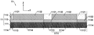
- Figure 7 is a schematic diagram of an embodiment of the wiring unit 11 in this application.
- Figure 8 is a schematic cross-sectional structural diagram of the wiring unit 11 shown in Figure 7 at C-C.
- the L first parts 1113 are provided with at least one first space 1115. It can be understood that the L first parts 1113 may be provided with one first space 1115 or multiple first spaces 1115. A plurality of first spaces 1115 are spaced apart from each other. The provision of the first space 1115 reduces the capacitance between the first wiring 1111 and the second wiring 1121, reduces the resistance and capacitance of the transmission unit, and improves the display performance of the display panel.
- the number of first parts 1113 is multiple, and the number of first spaces 1115 is also multiple.
- Each first portion 1113 is provided with a first space 1115 .
- there are multiple first parts 1113 and the multiple first parts 1113 are provided with one first space 1115 . That is to say, the L-1 first parts 1113 are not provided with the first spaces 1115.
- a first part 1113 may be provided with one first space 1115 or multiple first spaces 1115 .
- a plurality of first spaces 1115 provided in the same first portion 1113 are spaced apart from each other.
- the number of first spaces 1115 provided in each of the L first parts 1113 may be the same or different.
- M first traces 1111 have L first parts 1113, and the L first parts 1113 are provided with at least one first space 1115, including but not limited to the following implementations:
- each first trace 1111 has multiple first parts 1113 .
- Each first portion 1113 is provided with a first space 1115 .
- each first trace 1111 has multiple first parts 1113 .
- Each first portion 1113 is provided with a plurality of first spaces 1115 .
- each first trace 1111 has multiple first parts 1113 .
- Each first trace 1111 is provided with a first space 1115.
- the number of first traces 1111 is one, the number of second traces 1121 is multiple, and the first trace 1111 has multiple first portions 1113 .
- Each first portion 1113 is provided with a first space 1115 .
- the first space 1115 is a hole-like structure, and the central axis of the hole-like structure is perpendicular to the first wiring layer 111 .
- the overlapping area of the projection of the first part 1113 on the dielectric layer 113 and the projection of the second trace 1121 on the dielectric layer 113 is reduced, that is to say, the first trace 1111 and the second trace 1121 are directly opposite each other in the Z direction.
- the area is reduced, so that the planar capacitance between the first portion 1113 of the first trace 1111 and the second trace 1121 is reduced.
- the hole-like structure has a closed structure.
- the planar capacitance between the first part 1113 of the first trace 1111 and the second trace 1121 is further reduced. In this way, the resistance and capacitance of the transmission unit is reduced, and the display performance of the display panel is improved.
- FIG. 9 is a schematic diagram of another implementation of the wiring unit 11 shown in FIG. 8 .
- the first space 1115 may also be a groove structure, and the opening of the first space 1115 faces the second wiring 1121 .
- the groove structure can make the first trace 1111 have better strength.
- the thickness of the first part 1113 of the first trace 1111 in the direction perpendicular to the first wiring layer 111 decreases, so that the distance between the first part 1113 of the first trace 1111 and the second trace 1121 in the direction perpendicular to the first wiring layer 111
- the planar capacitance between the first portion 1113 of the first trace 1111 and the second trace 1121 can also be reduced.
- a dielectric material is disposed in the first space 1115 to form a first filling body 1116 .
- the material of the first filling body 1116 can be a common dielectric constant material such as SiO2, or a low dielectric constant material (low-k, LK) or an ultra-low dielectric constant material (ultra low-k, ULK). Or extremely low dielectric constant material (extreme low-k, ELK).
- the first space 1115 may not be filled with dielectric material.
- M first traces 1111 have K second portions 1114 .
- the projection of the K second portions 1114 on the dielectric layer 113 is staggered with the projection of the second traces 1121 on the dielectric layer 113 .
- the K second parts 1114 can be understood as the remaining parts of the M first traces 1111 except the L first parts 1113 .
- K second parts 1114 are provided with J second spaces 1117.
- J is an integer greater than or equal to 1. That is to say, the K second parts 1114 can be provided with one second space 1117, or multiple second spaces 1117. A plurality of second spaces 1117 are spaced apart from each other.
- some of the second parts 1114 of the K second parts 1114 may be provided with the second space 1117, or may not be provided with the second space 1117.
- a second portion 1114 can be provided with one second space 1117 or multiple second spaces 1117 .
- the number of second spaces 1117 provided in each of the K second parts 1114 may be equal or unequal.
- the projection of at least one of the J second spaces 1117 on the dielectric layer 113 coincides with the projection of the extension line of the second trace 1121 on the dielectric layer 113 .
- the projections of the J second spaces 1117 on the dielectric layer 113 all coincide with the projections of the extension lines of the second traces 1121 on the dielectric layer 113.
- second spaces 1117 are provided at positions where the projection of the extension lines of the N second traces 1121 on the dielectric layer 113 and the projection of the M first traces 1111 on the dielectric layer 113 coincide with each other. In this way, the resistances between the M first traces 1111 are similar, which reduces the delay difference of the driving signals between different first traces 1111, which is beneficial to improving the display performance of the display panel.
- the extension lines of part of the N second traces 1121 on the dielectric layer 113 overlap with the projection of the M first traces 1111 on the dielectric layer 113. Two spaces 1117.
- the shape of the second space 1117 may be a hole-like structure or a groove structure.
- the shape of the second space 1117 can be the same as the shape of the first space 1115, which can further reduce the impedance difference between the M first traces 1111, which is beneficial to reducing the driving signal delay between different first traces 1111. , improve the display performance of the display panel.
- the shape of the second space 1117 and the shape of the first space 1115 may also be different.
- a dielectric material is disposed in the second space 1117 to form a second filling body 1118 .
- the material of the second filling body 1118 can be a common dielectric constant material such as SiO2, or a low dielectric constant material (low-k, LK) or an ultra-low dielectric constant material (ultra low-k, ULK). Or extremely low dielectric constant material (extreme low-k, ELK).
- the second space 1117 may not be filled with dielectric material.
- the second part 1114 may not be provided with the second space 1117.
- FIG. 10 is a partial cross-sectional structural diagram of the wiring unit 11 in FIG. 4 .
- FIG. 11 is a schematic diagram of another embodiment of the wiring unit 11 in the present application.
- the thickness of dielectric layer 113 ranges from 3850 angstroms to 4350 angstroms. In an exemplary technique, referring to FIG. 10 , the thickness of dielectric layer 113 is generally in the range of 3350 angstroms to 3850 angstroms.
- this application can increase the distance between the first wiring 1111 and the second wiring 1121 in the Z direction by increasing the thickness of the dielectric layer 113 (see Figure 11), thereby reducing the distance between the first wiring 1111 and the second wiring 1121. and the planar capacitance between the second trace 1121.
- the thickness of the dielectric layer 113 ranges from increase to
- increasing the thickness of the dielectric layer 113 and setting the first space 1115 can be performed simultaneously. Based on the two factors that affect the planar capacitance, the spacing between the first wiring 1111 and the second wiring 1121 is increased or decreased. At the same time, the facing area is reduced, thereby reducing the planar capacitance. In one embodiment, increasing the thickness of the dielectric layer 113 and setting the first space 1115 and the second space 1117 can be performed simultaneously.
- the thickness of the insulating layer can also be increased, the distance between different wiring units 11 in the Z direction can be increased, and the planar capacitance between the first wiring 1111 and the second wiring 1121 of different wiring units 11 can be reduced.
- the dielectric layer 113 and the insulating layer are gate insulating layers.
- the wiring unit 11 is provided on the glass substrate 101 of the TFT substrate.
- the line width of the second trace 1121 is in the range of 10 microns to 13 microns (please refer to FIG. 12).
- the line width of the second trace 1121 is in the range of 15 microns to 20 microns.
- this application reduces the planar capacitance between the first wiring 1111 and the second wiring 1121 by reducing the line width of the second wiring 1121.
- the line width of the second trace 1121 is reduced from 15 ⁇ m to 13 ⁇ m.
- the line width of the second trace 1121 is in the range of 10 micrometers to 13 micrometers, and the thickness of the second trace 1121 is in the range of 4450 angstroms to 5000 angstroms.
- the thickness of the second trace 1121 ranges from 3800 to 4350. While reducing the line width of the second trace 1121, increase the thickness of the second trace 1121, keep the cross-sectional area of the second trace 1121 unchanged or increase it, to avoid the problem caused by the decrease in the line width of the second trace 1121. Resistance increases.
- the line width of the second trace 1121 is reduced from 15 ⁇ m to 13 ⁇ m, and the thickness of the second trace 1121 is reduced from 15 ⁇ m to 13 ⁇ m. increase to In one implementation, the line width of the first trace can also be reduced while increasing the thickness of the first trace.
Landscapes
- Physics & Mathematics (AREA)
- Nonlinear Science (AREA)
- General Physics & Mathematics (AREA)
- Engineering & Computer Science (AREA)
- Mathematical Physics (AREA)
- Chemical & Material Sciences (AREA)
- Crystallography & Structural Chemistry (AREA)
- Optics & Photonics (AREA)
- Computer Hardware Design (AREA)
- Theoretical Computer Science (AREA)
- Microelectronics & Electronic Packaging (AREA)
- Devices For Indicating Variable Information By Combining Individual Elements (AREA)
Abstract
本申请提供一种显示面板100及显示屏1000。显示面板100包括传输单元10和显示单元300。传输单元10电连接显示单元300。传输单元10包括第一布线层111、第二布线层112和介质层113。介质层113位于第一布线层111和第二布线层112之间。第一布线层111设有第一走线1111。第二布线层112设有第二走线1121。第一走线1111具有第一部分1113,第一部分1113在介质层113的投影与第二走线1121在介质层113的投影重合。第一部分1113设有第一空间1115。
Description
本申请要求于2022年04月21日提交中国专利局、申请号为202210422269.3,发明名称为“显示面板及显示屏”的中国专利申请的优先权,其全部内容通过引用结合在本申请中。
本申请涉及显示设备技术领域,尤其涉及一种显示面板及显示屏。
这里的陈述仅提供与本申请有关的背景信息,而不必然地构成现有技术。
随着人们对大尺寸窄边框显示屏的需求越来越强烈,无栅极驱动(Gate driver less,GDL)的显示面板越来越受到欢迎。然而,大尺寸超高清的面板内GDL走线尺寸增大,导致面板的电容电阻负载较大,面板的显示性能受到影响。
发明内容
本申请实施例提供一种低阻抗的显示面板及显示屏。
第一方面,本申请提供一种显示面板。显示面板包括传输单元和显示单元。传输单元电连接显示单元。传输单元用于将驱动信号输送至显示单元,以使显示单元显示图像。
传输单元包括第一布线层、第二布线层和介质层。介质层位于第一布线层和第二布线层之间。第一布线层设有M条第一走线。第二布线层设有N条第二走线。M条第一走线具有L个第一部分。L个第一部分在介质层的投影与第二走线在介质层的投影重合。第一走线通过第二走线电连接于显示单元。其中M、N、L均为大于等于1的整数。L个第一部分设有至少一个第一空间。
第二方面,本申请提供一种显示屏。显示屏包括背光模组和显示面板。背光模组设置为显示面板提供背光源。
显示面板包括传输单元和显示单元,传输单元电连接显示单元,传输单元用于将驱动信号输送至显示单元,以使显示单元显示图像。
传输单元包括第一布线层、第二布线层和介质层。介质层位于第一布线层和第二布线层之间,第一布线层设有M条第一走线,第二布线层设有N条第二 走线。M条第一走线具有L个第一部分,L个第一部分在介质层的投影与第二走线在介质层的投影重合,第一走线通过第二走线电连接于显示单元,其中M、N、L均为大于等于1的整数。L个第一部分设有至少一个第一空间。
可以理解的是,M条第一走线具有L个第一部分,第一部分在介质层的投影与第二走线在介质层的投影重合,在第一部分设置第一空间,这样可以减少第一走线与第二走线的正对面积,也就减少了第一走线与第二走线之间的平面电容。降低了传输单元的阻抗,显示面板的显示性能得到提升。
为了更清楚地说明本申请实施例的技术方案,下面将对实施例或现有技术描述中所需要使用的附图作简单地介绍,显而易见地,下面描述中的附图仅仅是本申请的一些实施例,对于本领域普通技术人员来讲,在不付出创造性劳动的前提下,还可以根据这些附图获得其他的附图。
图1是本实施例提供的显示屏的一种实施方式的结构示意图;
图2是驱动信号在显示面板的传输路径示意图;
图3是传输单元在Z方向的剖面结构示意图;
图4是现有技术中布线单元的部分结构示意图;
图5是图4中所示的布线单元在A-A处的剖面结构示意图
图6是图4中所示的布线单元在B-B处的剖面结构示意图
图7是本申请中布线单元一种实施方式示意图;
图8是图7中所示的布线单元在C-C处的剖面结构示意图;
图9是图8所示的布线单元的另一种实施方式示意图;
图10是图4中布线单元的部分剖面结构示意图;
图11是本申请中布线单元的又一种实施方式示意图;
图12是本申请中布线单元的再一种实施方式示意图。
下面将结合本申请实施例中的附图,对本申请实施例中的技术方案进行清楚、完整地描述,显然,所描述的实施例仅仅是本申请一部分实施例,而不是全部的实施例。基于本申请中的实施例,本领域普通技术人员在没有作出创造 性劳动前提下所获得的所有其他实施例,都属于本申请保护的范围。
除非另有定义,本文所使用的所有的技术和科学术语与属于本申请的技术领域的技术人员通常理解的含义相同。本文中在本申请的说明书中所使用的术语只是为了描述具体的实施例的目的,不是旨在于限制本申请。本文所使用的术语“及/或”包括一个或多个相关的所列项目的任意的和所有的组合。
需要说明的是,当一个元件被认为是“连接”另一个元件,它可以是直接连接到另一个元件或者可能同时存在居中元件。
下面结合附图,对本申请的具体实施方式进行详细描述。
请参阅图1,图1是本实施例提供的显示屏1000的一种实施方式的结构示意图。显示屏1000包括显示面板100以及背光模组200。背光模组200用于为显示面板100提供光源,以使显示面板100显示图像。
显示屏1000可以是液晶显示屏,还可以是OLED显示屏,W-OLED显示屏,QLED显示屏,等离子体显示屏,曲面型显示屏或其他类型显示屏。图1所示实施例的显示屏1000以液晶显示屏1000为例进行示意。液晶显示面板100可以包括彩色滤光片(colorfilter,CF)基板、薄膜场效应晶体管(Thin Film Transistor,TFT)基板、框胶以及液晶。
请再次参阅图1,显示面板100包括显示单元300和非显示单元400。非显示单元400位于显示单元300的周边。显示单元300用于显示图像。
请参阅图2,图2是驱动信号在显示面板100的传输路径示意图。显示面板100还包括传输单元10和GDL单元电路20。传输单元10和GDL单元电路20均设置于非显示单元400。传输单元10用于传输显示面板100的驱动信号。传输单元10电连接GDL单元电路20。GDL单元电路20电连接显示单元300。
在GDL驱动的显示面板100中,传输单元10用于将逻辑信号传输至GDL单元电路20,GDL单元电路20根据接收到信号向液晶面板输出扫描信号,以使显示单元300显示图像。
传输单元10和GDL单元电路20的数量可以相等,也可以不相等。本实施方式中,显示面板100采用双侧DGL驱动方式。即传输单元10和GDL单元电路20的数量均为两个,分别在显示单元300的相对的两侧。这样,两个传输单元10同时传输对应的驱动信号至同侧的GDL单元电路20,信号传输效率更高,有利于提高显示面板100的显示性能。在一种实施方式中,传输单元10和GDL 单元电路20的数量也可以为一个。在一种实施方式中,传输单元10和GDL单元电路20的数量也可以为两个以上。
在本实施方式中,传输单元10和GDL单元电路20对显示面板100提供横向驱动,即栅极驱动。在其他实施方式中,传输单元10和GDL单元电路20也可以对显示面板100提供源极驱动。
传输单元10包括时钟信号(CLOCK,CLK)走线、帧起始信号(Start Vertical,STV)走线、复位信号(Reset,RST)走线和低压逻辑信号(Vgatelow,VGL)走线中的一种或多种。
请参阅图3,图3是传输单元10在Z方向的剖面结构示意图。传输单元10包括多个布线单元11和至少一个绝缘层12。绝缘层12与布线单元11依次交替层叠设置,绝缘层12设置于相邻两个布线单元11之间,以使相邻布线单元11绝缘。在其他实施方式中,传输单元10也可以仅包括一个布线单元11,不设置绝缘层12。
绝缘层12填充有绝缘材料,绝缘材料可以为如SiO2等普通介电常数材料,也可以为低介电常数材料(low-k,LK)或超低介电常数材料(ultra low-k,ULK)或极低介电常数材料(extreme low-K,ELK)。
请参阅图4和图5,图4是现有技术中布线单元11的部分结构示意图,图5是图4中所示的布线单元11在A-A处的剖面结构示意图。布线单元11包括第一布线层111、第二布线层112和介质层113。第一布线层111、第二布线层112和介质层113层叠设置,介质层113设置于第一布线层111与第二布线层112之间。第一布线层111、第二布线层112和介质层113的数量均为一个。
请再次参阅图5,第一布线层111设有M条第一走线1111和第一绝缘介质1112,第一走线1111电连接驱动电路板。M条第一走线1111间隔设置,第一绝缘介质1112填充于M条第一走线1111的间隙之间,以使M条第一走线1111彼此绝缘。其中,M为大于等于1的整数。M条所述第一走线1111包括时钟信号(CLOCK,CLK)走线、帧起始信号(Start Vertical,STV)走线、复位信号(Reset,RST)走线和低压逻辑信号(Vgatelow,VGL)走线其中的一种或多种。
请再次参阅图5,第二布线层112设有N条第二走线1121和第二绝缘介质1122,第二走线1121一端电连接第一走线1111,第二走线1121另一端电连接 GDL单元电路20。N条第二走线1121间隔设置,第二绝缘介质1122填充于N条第二走线1121的间隙之间,以使N条第二走线1121彼此绝缘。其中,N为大于等于1的整数。
在一种实施方式中,同层的第一走线1111延伸方向一致,彼此平行间隔设置。同层的第二走线1121延伸方向一致,彼此平行间隔设置。同时第一走线1111延伸方向在介质层113的投影与第二走线1121延伸方向在介质层113的投影成一定夹角相交。
在本实施方式中,同时第一走线1111延伸方向在介质层113的投影与第二走线1121延伸方向在介质层113的投影垂直。
请再次参阅图5,介质层113设有H个通孔1131,H个通孔1131间隔设置。通孔1131内设有有导电材料。通孔1131贯穿介质层113,一端连接第一走线1111,另一端连接第二走线1121,第一走线1111通过通孔1131电连接第二走线1121。在一种实施方式中,通孔1131内填充有导电材料,形成金属柱1132。金属柱1132两端分别连接第一走线1111和第二走线1121。在其他实施方式中,通孔1131内仅仅在内壁设有导电材料。其中,H为大于等于1的整数。
请再次参阅图5,介质层113还包括第三绝缘介质1133,第三绝缘介质1133填充于H个通孔1131之间,以使通孔1131彼此之间绝缘。同时第三绝缘介质1133还能使第一布线层111与第二布线层112绝缘。这样,第一走线1111通过金属柱1132与第二走线1121电连接。第二走线1121与驱动单元电连接。本实施方式中,显示屏1000的驱动信号依次经过第一走线1111、金属柱1132、第二走线1121、GDL单元电路20,最后到达显示单元300。
在一种实施方式中,一条第一走线1111仅通过一个通孔1131电连接一条第二走线1121电。也就是说,第一走线1111、通孔1131、第二走线1121三者之间具有一对一的匹配关系。在其他实施方式中,两条第一走线1111通过两个通孔1131电连接同一条第二走线1121。或者是两条第二走线1121分别通过两个通孔1131电连接同一条第一走线1111。
另外,不同的布线单元11中的第一走线1111数量、第二走线1121数量和通孔1131数量可以一样,也可以不一样,本领域技术人员可以根据需求灵活设置。
第一走线1111、第二走线1121以及金属柱1132的材料可以为铜(Cu)、铝(Al)、 钨(W)、钴(Co)、银(Ag)、金(Au)、钌(Ru)、镍(Ni)等各种金属或者其合金。三者的材料可以相同,也可以不同。在本实施方式中,第一走线1111和第二走线1121为铜线,金属柱1132为Cu柱。在一种实施方式中,第一走线1111和第二走线1121为铜线,金属柱1132为Co柱。在一种实施方式中,第一走线1111为铜线,第二走线1121为铝线,金属柱1132为Co柱。
第一绝缘介质1112、第二绝缘介质1122以及第三绝缘介质1133可以为SiO2等普通介电常数材料,也可以为低介电常数材料(low-k,LK)或超低介电常数材料(ultra low-k,ULK)或极低介电常数材料(extreme low-K,ELK),以降低金属线之间的寄生电容及电路的互连线延迟。第一绝缘介质1112、第二绝缘介质1122以及第三绝缘介质1133的材料可以相同也可以不同,以满足对传输单元10的寄生电容、机械强度及可靠性等多方面的要求。在本实施方式中,第一绝缘介质1112、第二绝缘介质1122以及第三绝缘介质1133的材料相同。可以理解的是,相同的材料各个性能一致,第一布线层111、第二布线层112和介质层113之间不容易因外力作用产生裂缝,布线单元11整体强度较佳。
请参阅图6,图6是图4中所示的布线单元11在B-B处的剖面结构示意图。M条第一走线1111具有L个第一部分1113和K个第二部分1114。第一部分1113连接第二部分1114。L个第一部分1113彼此之间间隔设置。K个第二部分1114彼此之间间隔设置。其中,L个第一部分1113在介质层113的投影与第二走线1121在介质层113的投影重合,K个第二部分1114在介质层113的投影与第二走线1121在介质层113的投影错开。可以理解地是,第一部分1113为第二走线1121在第一布线层111的投影与第一走线1111的重合部分。其中,L、K为大于等于1的整数。
在一种实施方式中,第一走线1111数量为多条,M条第一走线1111可以每条第一走线1111均具有第一部分1113。在一种实施方式中,第一走线1111数量为多条,M条第一走线1111中部分第一走线1111具有第一部分1113,另外部分第一走线1111不具有第一部分1113。进一步的,M条第一走线1111中每条第一走线1111上具有第一部分1113的数量可以相等,也可以不相等。
请参阅图7和图8,图7是本申请中布线单元11一种实施方式示意图,图8是图7中所示的布线单元11在C-C处的剖面结构示意图。L个第一部分1113设有至少一个第一空间1115。可以理解地是,L个第一部分1113可以设有一个 第一空间1115,也可以设有多个第一空间1115。多个第一空间1115彼此间隔设置。第一空间1115的设置,减少了第一走线1111和第二走线1121之间的电容,降低了传输单元的阻容,显示面板的显示性能得到提升。
在一种实施方式中,第一部分1113的数量为多个,第一空间1115的数量也为多个。每个第一部分1113设有一个第一空间1115。在一种实施方式中,第一部分1113数量为多个,多个第一部分1113设有一个第一空间1115。也就是说,L-1个第一部分1113不设有第一空间1115。
进一步地,一个第一部分1113可以设有一个第一空间1115,也可以设有多个第一空间1115。设于同一个第一部分1113的多个第一空间1115彼此间隔设置。L个第一部分1113中每个第一部分1113设置的第一空间1115数量可以一样,也可以不一样。
总而言之,M条第一走线1111具有L个第一部分1113,L个第一部分1113设有至少一个第一空间1115,包括但不限于下述几种实施方式:
在一种实施方式中,第一走线1111和第二走线1121的数量均为多条,每条第一走线1111均具有多个第一部分1113。每个第一部分1113设有一个第一空间1115。
在一种实施方式中,第一走线1111和第二走线1121的数量均为多条,每条第一走线1111均具有多个第一部分1113。每个第一部分1113设有多个第一空间1115。
在一种实施方式中,第一走线1111和第二走线1121的数量均为多条,每条第一走线1111均具有多个第一部分1113。每条第一走线1111设有一个第一空间1115。
在一种实施方式中,第一走线1111的数量为一条,第二走线1121的数量为多条,第一走线1111具有多个第一部分1113。每个第一部分1113设有一个第一空间1115。
在本实施方式中,请再次参阅图8,第一空间1115为孔状结构,孔状结构中心轴线方向垂直第一布线层111。这样,第一部分1113在介质层113的投影与第二走线1121在介质层113的投影重叠面积减小,也就是说第一走线1111和第二走线1121的在Z方向上的正对面积减少,这样第一走线1111的第一部分1113和第二走线1121之间的平面电容减小。并且,孔状结构呈封闭结构,根 据电场屏蔽原理,第一走线1111的第一部分1113和第二走线1121之间的平面电容进一步减小。这样,降低了传输单元的阻容,显示面板的显示性能得到提升。
在一种实施方式中,请参阅图9,图9是图8所示的布线单元11的另一种实施方式示意图。第一空间1115也可以为凹槽结构,第一空间1115的开口朝向第二走线1121。可以理解地,与孔状结构相比,凹槽结构可以使得第一走线1111强度较佳。同时,第一走线1111的第一部分1113在垂直第一布线层111方向的厚度减小,这样第一走线1111的第一部分1113与第二走线1121在垂直第一布线层111方向的距离减小,也可以减小第一走线1111的第一部分1113和第二走线1121之间的平面电容。
在一种实施方式中,第一空间1115内设有介质材料,形成第一填充体1116。这样,第一走线1111的强度较佳,第一布线层111的整体强度更均匀。其中,第一填充体1116的材料可以为如SiO2等普通介电常数材料,也可以为低介电常数材料(low-k,LK)或超低介电常数材料(ultra low-k,ULK)或极低介电常数材料(extreme low-k,ELK)。在其他实施方式中,第一空间1115也可以不填充介质材料。
请再次参阅图7和图8,M条第一走线1111具有K个第二部分1114。K个第二部分1114在介质层113的投影与第二走线1121在介质层113的投影错开。K个第二部分1114可以理解为M条第一走线1111除L个第一部分1113以外的剩余部分。
K个第二部分1114设有J个第二空间1117。其中,J为大于等于1的整数。也就是说,K个第二部分1114可以设置一个第二空间1117,也可以设置多个第二空间1117。多个第二空间1117彼此间隔设置。
在一种实施方式中,K个第二部分1114其中的部分第二部分1114可以设置第二空间1117,也可以不设置第二空间1117。在一种实施方式中,一个第二部分1114可以设置一个第二空间1117,也可以设置多个第二空间1117。K个第二部分1114中每个第二部分1114设有的第二空间1117数量可以相等,也可以不相等。
J个第二空间1117中至少一个在介质层113的投影与第二走线1121的延长线在介质层113的投影重合。在一种实施方式中,J个第二空间1117在介质层 113的投影全部与第二走线1121的延长线在介质层113的投影重合。
在一种实施方式中,N条第二走线1121的延长线在介质层113的投影与M条第一走线1111在介质层113的投影的重合位置均设有第二空间1117。这样,M条第一走线1111的之间的电阻相近,拉进不同第一走线1111之间的驱动信号延迟差异,有利于提高显示面板的显示性能。
在一种实施方式中,N条第二走线1121中部分第二走线1121的延长线在介质层113的投影与M条第一走线1111在介质层113的投影的重合位置设有第二空间1117。
第二空间1117的形状可以为孔状结构,也可以为凹槽结构。第二空间1117的形状可以与第一空间1115的形状一样,这样可以进一步拉进M条第一走线1111彼此之间的阻抗差异,有利于降低不同第一走线1111之间的驱动信号延迟,提高显示面板的显示性能。在其他实施方式中,第二空间1117的形状与第一空间1115的形状也可以不一样。
在本实施方式中,第二空间1117内设有介质材料,形成第二填充体1118。这样,第一走线1111的强度较佳,第一布线层111的整体强度更均匀。其中,第二填充体1118的材料可以为如SiO2等普通介电常数材料,也可以为低介电常数材料(low-k,LK)或超低介电常数材料(ultra low-k,ULK)或极低介电常数材料(extreme low-k,ELK)。在其他实施方式中,第二空间1117也可以不填充介质材料。
在一种实施方式中,第二部分1114也可以不设置第二空间1117。
请参阅图10和图11,图10是图4中布线单元11的部分剖面结构示意图,图11是本申请中布线单元11的又一种实施方式示意图。在一种实施方式中,介质层113的厚度在3850埃至4350埃的范围内。在示例性技术中,请参阅图10,介质层113厚度一般为3350埃至3850埃范围内。根据平面电容形成原理,本申请通过增加介质层113的厚度(请参阅图11),可以增加第一走线1111与第二走线1121在Z方向上的距离,进而减小第一走线1111和第二走线1121之间的平面电容。在一种实施方式中,介质层113的厚度从
 增加到
增加到

在一种实施方式中,增加介质层113厚度和设置第一空间1115可以同时进行,从影响平面电容的两个因素出发,增减第一走线1111和第二走线1121之间的间距的同时减少正对面积,从而减小平面电容。在一种实施方式中,增加介 质层113厚度、设置第一空间1115和第二空间1117可以同时进行。
在一种实施方式中,还可以增加绝缘层的厚度,可以增加不同布线单元11在Z方向上的距离,减少不同布线单元11的第一走线1111和第二走线1121之间的平面电容。在一种实施方式中,介质层113和绝缘层为栅极绝缘层。布线单元11设置在TFT基板的玻璃基板101上。
请参阅图12,图12是本申请中布线单元11的再一种实施方式示意图。在一种实施方式中,第二走线1121的线宽在10微米至13微米的范围(请参阅图12)。在示例性技术中,(请参阅图10),第二走线1121的线宽在15微米至20微米的范围。根据平面电容形成原理,本申请通过减小第二走线1121的线宽,进而减小第一走线1111和第二走线1121之间的平面电容。在一种实施方式中,第二走线1121的线宽从15μm减少至13μm。
在一种实施方式中,第二走线1121的线宽在10微米至13微米的范围,第二走线1121的厚度在4450埃至5000埃的范围。在示例性技术中,(请参阅图10),第二走线1121的厚度在3800至4350的范围。在减小第二走线1121线宽的同时增加第二走线1121的厚度,保持第二走线1121的横截面积不变或者增加,避免由于第二走线1121的线宽减小而导致电阻增加。在一种实施方式中,第二走线1121的线宽从15μm减少至13μm,第二走线1121的厚度从
 增加到
增加到
 在一种实施方式中,也可以减小第一走线的线宽同时增加第一走线的厚度。
以上,仅为本申请的具体实施方式,但本申请的保护范围并不局限于此,任何熟悉本技术领域的技术人员在本申请揭露的技术范围内,可轻易想到变化或替换,都应涵盖在本申请的保护范围之内;在不冲突的情况下,本申请的实施例及实施例中的特征可以相互组合。因此,本申请的保护范围应以权利要求的保护范围为准。
Claims (15)
- 一种显示面板,包括传输单元和显示单元,所述传输单元电连接所述显示单元,所述传输单元用于将驱动信号输送至所述显示单元,以使所述显示单元显示图像;所述传输单元包括第一布线层、第二布线层和介质层,所述介质层位于所述第一布线层和所述第二布线层之间,所述第一布线层设有M条第一走线,所述第二布线层设有N条第二走线,M条所述第一走线具有L个第一部分,L个所述第一部分在介质层的投影与所述第二走线在介质层的投影重合,所述第一走线通过所述第二走线电连接于所述显示单元,其中M、N、L均为大于等于1的整数;L个所述第一部分设有至少一个第一空间。
- 根据权利要求1所述的显示面板,其中,所述第一空间为孔状结构或者凹槽结构。
- 根据权利要求1所述的显示面板,其中,所述第一走线与所述第二走线的数量均为多条,每条所述第一走线至少具有一个第一部分,每条所述第一走线设有至少一个第一空间。
- 根据权利要求1所述的显示面板,其中,M条所述第一走线包括K个第二部分,所述第二部分连接所述第一部分,所述第二部分在介质层的投影与所述第二走线在第一介质层的投影错开,K个所述第二部分设有J个第二空间,J个所述第二空间中至少一个在介质层的投影与第二走线的延长线在介质层的投影重合,其中K、J均为大于等于1的整数。
- 根据权利要求4所述的显示面板,其中,J个所述第二空间在介质层的投影均与第二走线的延长线在介质层的投影重合。
- 根据权利要求1所述的显示面板,其中,所述介质层的厚度在3850埃至4350埃的范围。
- 根据权利要求1所述的显示面板,其中,所述第二走线的线宽在10微米至13微米的范围,所述第二走线的厚度在4450埃至5000埃的范围。
- 根据权利要求1所述的显示面板,其中,所述第一布线层、所述介质层和所述第二布线层构成布线单元,所述布线单元为多个;所述传输单元还包括至少一个绝缘层,所述布线单元和所述绝缘层依次交替层叠设置,所述绝缘层位于两个相邻所述布线单元之间,以使相邻所述布线单元绝缘。
- 根据权利要求1所述的显示面板,其中,M条所述第一走线包括时钟信号走线、帧起始信号走线、复位信号走线和低压逻辑信号走线其中的一种或多种。
- 根据权利要求2所述的显示面板,其中,所述第一空间内设有介质材料。
- 根据权利要求3所述的显示面板,其中,每个所述第一部分上均设有一个第一空间。
- 根据权利要求4所述的显示面板,其中,所述第二空间为孔状结构或者凹槽结构。
- 根据权利要求1所述的显示面板,其中,所述介质层设有通孔,所述通孔内设有导电材料;所述第一走线通过所述通孔电连接于所述第二走线。
- 根据权利要求1所述的显示面板,其中,所述传输单元的数量为多个,多个所述传输单元分布在所述显示单元的周边。
- 一种显示屏,包括背光模组和显示面板,所述背光模组设置为所述显示面板提供背光源;显示面板包括传输单元和显示单元,所述传输单元电连接所述显示单元,所述传输单元用于将驱动信号输送至所述显示单元,以使所述显示单元显示图 像;所述传输单元包括第一布线层、第二布线层和介质层,所述介质层位于所述第一布线层和所述第二布线层之间,所述第一布线层设有M条第一走线,所述第二布线层设有N条第二走线,M条所述第一走线具有L个第一部分,L个所述第一部分在介质层的投影与所述第二走线在介质层的投影重合,所述第一走线通过所述第二走线电连接于所述显示单元,其中M、N、L均为大于等于1的整数;L个所述第一部分设有至少一个第一空间。
Applications Claiming Priority (2)
| Application Number | Priority Date | Filing Date | Title |
|---|---|---|---|
| CN202210422269.3 | 2022-04-21 | ||
| CN202210422269.3A CN114740664B (zh) | 2022-04-21 | 2022-04-21 | 显示面板及显示屏 |
Publications (1)
| Publication Number | Publication Date |
|---|---|
| WO2023202089A1 true WO2023202089A1 (zh) | 2023-10-26 |
Family
ID=82283712
Family Applications (1)
| Application Number | Title | Priority Date | Filing Date |
|---|---|---|---|
| PCT/CN2022/137260 Ceased WO2023202089A1 (zh) | 2022-04-21 | 2022-12-07 | 显示面板及显示屏 |
Country Status (3)
| Country | Link |
|---|---|
| US (1) | US12181762B2 (zh) |
| CN (1) | CN114740664B (zh) |
| WO (1) | WO2023202089A1 (zh) |
Families Citing this family (2)
| Publication number | Priority date | Publication date | Assignee | Title |
|---|---|---|---|---|
| CN114740664B (zh) * | 2022-04-21 | 2023-04-28 | 绵阳惠科光电科技有限公司 | 显示面板及显示屏 |
| CN120108293A (zh) * | 2025-02-28 | 2025-06-06 | 惠科股份有限公司 | 显示面板、显示装置以及显示面板的修复方法 |
Citations (6)
| Publication number | Priority date | Publication date | Assignee | Title |
|---|---|---|---|---|
| US20020067452A1 (en) * | 1999-01-29 | 2002-06-06 | Nec Corporation | Active matrix liquid-crystal display device |
| CN109298576A (zh) * | 2018-11-29 | 2019-02-01 | 惠科股份有限公司 | 阵列基板和显示面板 |
| CN109407435A (zh) * | 2018-11-29 | 2019-03-01 | 惠科股份有限公司 | 阵列基板和显示面板 |
| CN109491161A (zh) * | 2018-11-29 | 2019-03-19 | 惠科股份有限公司 | 阵列基板和显示面板 |
| CN211238253U (zh) * | 2019-12-20 | 2020-08-11 | 京东方科技集团股份有限公司 | 一种阵列基板、显示面板和显示装置 |
| CN114740664A (zh) * | 2022-04-21 | 2022-07-12 | 绵阳惠科光电科技有限公司 | 显示面板及显示屏 |
Family Cites Families (14)
| Publication number | Priority date | Publication date | Assignee | Title |
|---|---|---|---|---|
| JP4014588B2 (ja) * | 2004-09-10 | 2007-11-28 | 株式会社フューチャービジョン | 表示装置用の基板およびこの基板を用いた表示装置 |
| KR101201068B1 (ko) * | 2005-12-20 | 2012-11-14 | 엘지디스플레이 주식회사 | 액정 표시 장치 및 그 제조방법 |
| KR101582945B1 (ko) * | 2009-11-18 | 2016-01-08 | 삼성디스플레이 주식회사 | 액정 표시 장치 |
| CN106802507B (zh) * | 2017-04-01 | 2019-04-30 | 厦门天马微电子有限公司 | 一种显示面板和触控显示装置 |
| CN107479227A (zh) * | 2017-07-06 | 2017-12-15 | 惠科股份有限公司 | 一种电路板及其制作方法 |
| CN108549170B (zh) * | 2018-06-01 | 2021-04-27 | 上海天马微电子有限公司 | 一种显示面板以及电子设备 |
| CN208938618U (zh) * | 2018-11-08 | 2019-06-04 | 信利半导体有限公司 | 显示驱动芯片及显示面板 |
| WO2020210932A1 (zh) * | 2019-04-15 | 2020-10-22 | 华为技术有限公司 | 电容器和半导体芯片 |
| KR102777685B1 (ko) * | 2019-05-02 | 2025-03-11 | 삼성디스플레이 주식회사 | 표시장치 |
| CN111384066B (zh) * | 2020-03-19 | 2022-03-08 | 京东方科技集团股份有限公司 | 阵列基板、显示装置 |
| CN113764460B (zh) * | 2020-06-01 | 2025-02-25 | 京东方科技集团股份有限公司 | 显示基板和显示装置 |
| KR102812259B1 (ko) * | 2020-07-10 | 2025-05-27 | 삼성디스플레이 주식회사 | 표시장치 |
| CN113013213A (zh) * | 2021-02-26 | 2021-06-22 | 钱梅英 | 一种显示面板以及显示装置 |
| CN113325637A (zh) * | 2021-05-31 | 2021-08-31 | Tcl华星光电技术有限公司 | 显示面板 |
-
2022
- 2022-04-21 CN CN202210422269.3A patent/CN114740664B/zh active Active
- 2022-12-07 WO PCT/CN2022/137260 patent/WO2023202089A1/zh not_active Ceased
- 2022-12-28 US US18/089,951 patent/US12181762B2/en active Active
Patent Citations (6)
| Publication number | Priority date | Publication date | Assignee | Title |
|---|---|---|---|---|
| US20020067452A1 (en) * | 1999-01-29 | 2002-06-06 | Nec Corporation | Active matrix liquid-crystal display device |
| CN109298576A (zh) * | 2018-11-29 | 2019-02-01 | 惠科股份有限公司 | 阵列基板和显示面板 |
| CN109407435A (zh) * | 2018-11-29 | 2019-03-01 | 惠科股份有限公司 | 阵列基板和显示面板 |
| CN109491161A (zh) * | 2018-11-29 | 2019-03-19 | 惠科股份有限公司 | 阵列基板和显示面板 |
| CN211238253U (zh) * | 2019-12-20 | 2020-08-11 | 京东方科技集团股份有限公司 | 一种阵列基板、显示面板和显示装置 |
| CN114740664A (zh) * | 2022-04-21 | 2022-07-12 | 绵阳惠科光电科技有限公司 | 显示面板及显示屏 |
Also Published As
| Publication number | Publication date |
|---|---|
| CN114740664A (zh) | 2022-07-12 |
| US12181762B2 (en) | 2024-12-31 |
| CN114740664B (zh) | 2023-04-28 |
| US20230341733A1 (en) | 2023-10-26 |
Similar Documents
| Publication | Publication Date | Title |
|---|---|---|
| CN113555375B (zh) | 显示设备 | |
| CN108388054B (zh) | 显示面板与显示装置 | |
| CN207557624U (zh) | 一种阵列基板、显示面板及显示装置 | |
| CN109860253B (zh) | 一种柔性显示面板及柔性显示装置 | |
| CN108023028A (zh) | 背板基板和使用背板基板的柔性显示器 | |
| CN102253507A (zh) | 芯片扇出设计、其形成方法及使用所述设计的液晶显示器 | |
| CN111755479B (zh) | 显示装置 | |
| WO2023202089A1 (zh) | 显示面板及显示屏 | |
| CN107833895A (zh) | 显示面板及其制造方法、显示装置 | |
| CN115657352A (zh) | 显示面板及显示装置 | |
| CN115662330A (zh) | 一种显示面板和显示装置 | |
| TWI700535B (zh) | 畫素陣列基板 | |
| CN115762382A (zh) | 一种显示面板和显示装置 | |
| WO2023108847A1 (zh) | 显示面板及显示装置 | |
| WO2018101159A1 (ja) | 接続用配線 | |
| CN112151556B (zh) | 显示面板、显示装置及显示面板的制备方法 | |
| CN106842733B (zh) | 显示面板及其阵列基板 | |
| CN115881024A (zh) | 一种显示基板及显示装置 | |
| WO2024000794A1 (zh) | 显示面板及显示终端 | |
| WO2021129159A1 (zh) | 柔性显示面板和曲面显示屏 | |
| CN112802866A (zh) | 背光源制备方法,背光源及显示装置 | |
| CN118073367A (zh) | 显示面板及显示装置 | |
| US7847875B2 (en) | Anti-interference wiring assembly for liquid crystal display device and method for reducing interference | |
| CN111090201B (zh) | 显示面板及电子装置 | |
| CN206479746U (zh) | 阵列基板及具有该阵列基板的显示装置 |
Legal Events
| Date | Code | Title | Description |
|---|---|---|---|
| 121 | Ep: the epo has been informed by wipo that ep was designated in this application |
Ref document number: 22938307 Country of ref document: EP Kind code of ref document: A1 |
|
| NENP | Non-entry into the national phase |
Ref country code: DE |
|
| 122 | Ep: pct application non-entry in european phase |
Ref document number: 22938307 Country of ref document: EP Kind code of ref document: A1 |