WO2023199639A1 - 半導体装置 - Google Patents
半導体装置 Download PDFInfo
- Publication number
- WO2023199639A1 WO2023199639A1 PCT/JP2023/007947 JP2023007947W WO2023199639A1 WO 2023199639 A1 WO2023199639 A1 WO 2023199639A1 JP 2023007947 W JP2023007947 W JP 2023007947W WO 2023199639 A1 WO2023199639 A1 WO 2023199639A1
- Authority
- WO
- WIPO (PCT)
- Prior art keywords
- terminal
- conductive plate
- semiconductor device
- case
- semiconductor elements
- Prior art date
- Legal status (The legal status is an assumption and is not a legal conclusion. Google has not performed a legal analysis and makes no representation as to the accuracy of the status listed.)
- Ceased
Links
Images













Classifications
-
- H—ELECTRICITY
- H02—GENERATION; CONVERSION OR DISTRIBUTION OF ELECTRIC POWER
- H02M—APPARATUS FOR CONVERSION BETWEEN AC AND AC, BETWEEN AC AND DC, OR BETWEEN DC AND DC, AND FOR USE WITH MAINS OR SIMILAR POWER SUPPLY SYSTEMS; CONVERSION OF DC OR AC INPUT POWER INTO SURGE OUTPUT POWER; CONTROL OR REGULATION THEREOF
- H02M7/00—Conversion of AC power input into DC power output; Conversion of DC power input into AC power output
- H02M7/003—Constructional details, e.g. physical layout, assembly, wiring or busbar connections
-
- H—ELECTRICITY
- H02—GENERATION; CONVERSION OR DISTRIBUTION OF ELECTRIC POWER
- H02M—APPARATUS FOR CONVERSION BETWEEN AC AND AC, BETWEEN AC AND DC, OR BETWEEN DC AND DC, AND FOR USE WITH MAINS OR SIMILAR POWER SUPPLY SYSTEMS; CONVERSION OF DC OR AC INPUT POWER INTO SURGE OUTPUT POWER; CONTROL OR REGULATION THEREOF
- H02M7/00—Conversion of AC power input into DC power output; Conversion of DC power input into AC power output
- H02M7/42—Conversion of DC power input into AC power output without possibility of reversal
- H02M7/44—Conversion of DC power input into AC power output without possibility of reversal by static converters
- H02M7/48—Conversion of DC power input into AC power output without possibility of reversal by static converters using discharge tubes with control electrode or semiconductor devices with control electrode
- H02M7/53—Conversion of DC power input into AC power output without possibility of reversal by static converters using discharge tubes with control electrode or semiconductor devices with control electrode using devices of a triode or transistor type requiring continuous application of a control signal
- H02M7/537—Conversion of DC power input into AC power output without possibility of reversal by static converters using discharge tubes with control electrode or semiconductor devices with control electrode using devices of a triode or transistor type requiring continuous application of a control signal using semiconductor devices only, e.g. single switched pulse inverters
-
- H—ELECTRICITY
- H02—GENERATION; CONVERSION OR DISTRIBUTION OF ELECTRIC POWER
- H02M—APPARATUS FOR CONVERSION BETWEEN AC AND AC, BETWEEN AC AND DC, OR BETWEEN DC AND DC, AND FOR USE WITH MAINS OR SIMILAR POWER SUPPLY SYSTEMS; CONVERSION OF DC OR AC INPUT POWER INTO SURGE OUTPUT POWER; CONTROL OR REGULATION THEREOF
- H02M7/00—Conversion of AC power input into DC power output; Conversion of DC power input into AC power output
- H02M7/42—Conversion of DC power input into AC power output without possibility of reversal
- H02M7/44—Conversion of DC power input into AC power output without possibility of reversal by static converters
- H02M7/48—Conversion of DC power input into AC power output without possibility of reversal by static converters using discharge tubes with control electrode or semiconductor devices with control electrode
- H02M7/53—Conversion of DC power input into AC power output without possibility of reversal by static converters using discharge tubes with control electrode or semiconductor devices with control electrode using devices of a triode or transistor type requiring continuous application of a control signal
- H02M7/537—Conversion of DC power input into AC power output without possibility of reversal by static converters using discharge tubes with control electrode or semiconductor devices with control electrode using devices of a triode or transistor type requiring continuous application of a control signal using semiconductor devices only, e.g. single switched pulse inverters
- H02M7/5387—Conversion of DC power input into AC power output without possibility of reversal by static converters using discharge tubes with control electrode or semiconductor devices with control electrode using devices of a triode or transistor type requiring continuous application of a control signal using semiconductor devices only, e.g. single switched pulse inverters in a bridge configuration
-
- H—ELECTRICITY
- H10—SEMICONDUCTOR DEVICES; ELECTRIC SOLID-STATE DEVICES NOT OTHERWISE PROVIDED FOR
- H10W—GENERIC PACKAGES, INTERCONNECTIONS, CONNECTORS OR OTHER CONSTRUCTIONAL DETAILS OF DEVICES COVERED BY CLASS H10
- H10W90/00—Package configurations
Definitions
- the present invention relates to a semiconductor device.
- the V- terminal is connected to the V+ terminal.
- a known technique is to form a current loop at a higher position than the current loop and reduce inductance by canceling the magnetic flux (Patent Document 1).
- a conductive layer on which the semiconductor element group on the upper arm side of the inverter circuit is arranged and to which the positive terminal is connected a conductive layer on which the semiconductor element group on the lower arm side is arranged and the output terminal is connected, and a conductive layer to which the negative terminal is connected.
- Power modules are known that include a circuit board that includes a conductive layer. Regarding such a power module, the main current flowing from the positive terminal is divided into two parts, and is sent to the conductive layer where the semiconductor element group on the upper arm side is arranged, and then passes through the semiconductor element group on the upper arm side to the lower arm side.
- a technique is known in which the current flows through a conductive layer where a group of semiconductor elements is arranged, and then flows through a conductive layer to which a negative electrode terminal is connected via the semiconductor element group on the lower arm side.
- a technique is known in which the inductance between PN is reduced by arranging a circuit board layout such that main currents flow in parallel, adjacent, and opposite directions (Patent Documents 2 to 4).
- the semiconductor switching elements on the upper and lower arm sides are each arranged on a collector pattern arranged on an insulating board, the collector is arranged on the collector pattern, and the emitter is connected to the emitter pattern arranged on the insulating board by an emitter wire.
- Semiconductor modules are known. Regarding such a semiconductor module, a positive electrode is connected to the collector pattern on the upper arm side, a negative electrode is connected to the emitter pattern on the lower arm side, and a portion of the positive electrode and a portion of the negative electrode parallel to the insulating plate are connected. , a technique is known in which they are arranged so as to be superimposed when viewed from the vertical direction (Patent Document 5).
- reducing the inductance between PN is effective from the viewpoint of suppressing surge voltage.
- the main current wiring such as the OUT terminal, P terminal, and N terminal, as well as the layout of the conductive plate to which the main current wiring is connected together with the semiconductor elements that constitute the semiconductor device, it is not possible to sufficiently reduce the inductance between PN. In some cases, the performance of the semiconductor device may not be fully demonstrated. With conventional techniques, there have been cases in which it has not been possible to realize a high-performance semiconductor device in which the inductance between PN is sufficiently reduced and the performance of the semiconductor element is fully exhibited.
- the present invention aims to realize a high-performance semiconductor device.
- a plurality of semiconductor elements each having a first electrode on a first main surface and a second electrode on a second main surface opposite to the first main surface, and a case having a conductive plate electrically connected to a first electrode, one side, and a side opposite to the one side, and containing the plurality of semiconductor elements and the conductive plate; a trunk disposed inside and outside the case and extending from one side of the case to the inside of the case; and a trunk branched from the trunk in plan view and electrically connected to the second electrodes of the plurality of semiconductor elements.
- a semiconductor device includes a second main current wiring that has a second extension part sandwiched between a second branch part and is electrically connected to the conductive plate.
- a substrate a case in which the substrate is arranged, a plurality of first semiconductor elements arranged inside the case, and a plurality of second semiconductor elements arranged inside the case.
- a first conductive plate disposed on the substrate and electrically connected to the plurality of first semiconductor elements
- a first conductive plate disposed on the substrate and electrically connected to the plurality of second semiconductor elements.
- 2 conductive plates, a first external terminal section disposed outside the case, and a first extension section, a first connection section, and a second connection section disposed inside the case, the first The extending portion connects the first external terminal portion, the first connecting portion, and the second connecting portion to each other, and the first connecting portion and the second connecting portion electrically connect to the first conductive plate.
- a first main current wiring to be connected a second external terminal section disposed outside the case, and a second extension section and a third connection section disposed inside the case;
- a second extension part connects the second external terminal part and the third connection part to each other, and the third connection part is electrically connected to the second conductive plate, and a second main current wiring;
- the first connection part and the second connection part are arranged to sandwich the second extension part, and a power supply voltage is applied to one of the first main current wiring and the second main current wiring.
- FIG. 1 is a diagram (part 1) illustrating an example of a semiconductor device according to a first embodiment
- FIG. 2 is a diagram (part 2) illustrating an example of the semiconductor device according to the first embodiment
- FIG. 3 is a diagram (Part 3) illustrating an example of the semiconductor device according to the first embodiment
- FIG. 2 is a diagram (part 1) illustrating the flow of main current during operation of the semiconductor device according to the first embodiment.
- FIG. 2 is a diagram (part 2) illustrating the flow of main current during operation of the semiconductor device according to the first embodiment;
- FIG. 7 is a diagram (part 1) illustrating an example of a semiconductor device according to a second embodiment
- FIG. 7 is a diagram (part 2) illustrating an example of the semiconductor device according to the second embodiment.
- FIG. 3 is a diagram (part 3) illustrating an example of the semiconductor device according to the second embodiment;
- FIG. 7 is a diagram (part 1) illustrating an example of a semiconductor device according to a third embodiment;
- FIG. 7 is a diagram (part 2) illustrating an example of a semiconductor device according to a third embodiment;
- FIG. 7 is a diagram (Part 3) illustrating an example of a semiconductor device according to a third embodiment;
- FIG. 7 is a diagram illustrating an example of a semiconductor device according to a fourth embodiment.
- FIG. 1 illustrating an example of a semiconductor device according to a second embodiment
- FIG. 7 is a diagram (part 2) illustrating an example of the semiconductor device according to the second embodiment.
- FIG. 3 is a diagram (part 3) illustrating an example of the semiconductor
- FIG. 7 is a diagram illustrating another example of the semiconductor device according to the fourth embodiment.
- FIG. 7 is a diagram (part 1) illustrating an example of a semiconductor device according to a fifth embodiment
- FIG. 7 is a diagram (part 2) illustrating an example of the semiconductor device according to the fifth embodiment
- FIG. 7 is a diagram (part 3) illustrating an example of a semiconductor device according to a fifth embodiment
- FIG. 7 is a diagram (part 1) illustrating an example of a semiconductor device according to a sixth embodiment
- FIG. 7 is a diagram (part 2) illustrating an example of a semiconductor device according to a sixth embodiment
- FIG. 7 is a diagram (part 3) illustrating an example of a semiconductor device according to a sixth embodiment
- FIG. 4 is a diagram (part 4) illustrating an example of a semiconductor device according to a sixth embodiment
- FIG. 7 is a diagram (part 1) illustrating an example of a semiconductor device according to a seventh embodiment
- FIG. 7 is a diagram (part 2) illustrating an example of a semiconductor device according to a seventh embodiment
- FIG. 7 is a diagram (part 3) illustrating an example of a semiconductor device according to a seventh embodiment
- FIG. 4 is a diagram (part 4) illustrating an example of a semiconductor device according to a seventh embodiment
- FIG. 12 is a diagram illustrating an example of the arrangement of main current wiring in a semiconductor device according to an eighth embodiment.
- FIG. 7 is a diagram illustrating a first example of a semiconductor device according to an eighth embodiment.
- FIG. 7 is a diagram illustrating a second example of a semiconductor device according to an eighth embodiment.
- FIG. 7 is a diagram illustrating a third example of a semiconductor device according to an eighth embodiment.
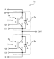
- FIG. 1 is a first example of a circuit diagram of a semiconductor device.
- FIG. 1 shows a circuit diagram of a semiconductor device 1a that constitutes an inverter circuit.
- the semiconductor device 1a includes a semiconductor element 2 and a semiconductor element 3 connected in series.
- a switching element such as an IGBT (Insulated Gate Bipolar Transistor) or a MOSFET (Metal Oxide Semiconductor Field Effect Transistor) is used for the semiconductor element 2 and the semiconductor element 3, respectively.
- a diode element such as an FWD (Free Wheeling Diode) or an SBD (Schottky Barrier Diode) may be connected to each of the switch elements used in the semiconductor element 2 and the semiconductor element 3.
- FWD Free Wheeling Diode
- SBD Schottky Barrier Diode
- an RC (Reverse Conducting)-IGBT in which an IGBT 2a and an FWD 2b are connected is used as the semiconductor element 2
- an RC-IGBT in which an IGBT 3a and an FWD 3b are connected is used as the semiconductor element 3.
- the collector C of the IGBT 2a and the cathode K of the FWD 2b are connected, and the emitter E of the IGBT 2a and the anode A of the FWD 2b are connected.
- the collector C of the IGBT 3a and the cathode K of the FWD 3b are connected, and the emitter E of the IGBT 3a and the anode A of the FWD 3b are connected.
- Emitter E of IGBT 2a of semiconductor element 2 and collector C of IGBT 3a of semiconductor element 3 are connected.
- Gates G of IGBT2a and IGBT3a are connected to gate terminal G1 and gate terminal G2, respectively.
- Emitters E of IGBT2a and IGBT3a are connected to sense emitter terminal E1 and sense emitter terminal E2, respectively.
- the semiconductor element 2 constitutes the upper arm of the semiconductor device 1a that constitutes the inverter circuit.
- the semiconductor element 3 constitutes a lower arm of the semiconductor device 1a that constitutes an inverter circuit.
- a collector C of the semiconductor element 2 is connected to a positive electrode (P) terminal to which a high potential side power supply voltage is input.
- An emitter E of the semiconductor element 3 is connected to a negative (N) terminal to which a low-potential side power supply voltage is input.
- a connection node between the semiconductor element 2 and the semiconductor element 3 connected in series is connected to an output (OUT) terminal from which an output current is output.
- the P terminal, N terminal, and OUT terminal are also respectively referred to as main current wiring.
- the collector C of the semiconductor element 2 is further configured to sense the voltage Vce between the collector C and the emitter E of the semiconductor element 2 (or the voltage Vds between the drain and the source) by using it in parallel with the sense emitter terminal E1.
- the SP terminal is a terminal for determining that an overcurrent due to a saturated state is flowing through the semiconductor element 2 if the current is equal to or higher than a predetermined value when the semiconductor element 2 is turned on.
- the semiconductor element 2 constituting the upper arm is not limited to one including one set of IGBT 2a and FWD 2b, but may be one in which a plurality of sets including one set of IGBT 2a and FWD 2b are connected in parallel.
- the semiconductor element 3 constituting the lower arm is not limited to one including one set of IGBT 3a and FWD 3b, but may be one in which a plurality of sets including one set of IGBT 3a and FWD 3b are connected in parallel.
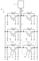
- FIG. 2 is a second example of a circuit diagram of a semiconductor device.
- FIG. 2 shows a circuit diagram of a semiconductor device 1b that constitutes a three-phase voltage source inverter circuit of U phase, V phase, and W phase.
- Three semiconductor devices 1a as shown in FIG. 1 are connected in parallel between the PN terminals to realize a semiconductor device 1b as shown in FIG.
- the OUT terminals (FIG. 1) of the three semiconductor devices 1a correspond to the U-phase, V-phase, and W-phase output nodes of the semiconductor device 1b constituting the three-phase voltage source inverter circuit, respectively, and are connected to a load 4 such as a motor. Connected.
- RC-IGBT is illustrated as the semiconductor element 2 and the semiconductor element 3.
- RB (Reverse Blocking)-IGBT may be used as the semiconductor element 2 and the semiconductor element 3.
- the semiconductor element 2 including the IGBT 2a and the FWD 2b, and the semiconductor element 3 including the IGBT 3a and the FWD 3b are illustrated.
- other switching elements such as MOSFETs may be used instead of IGBT2a and IGBT3a, and other diode elements such as SBD may be used instead of FWD2b and FWD3b.
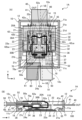
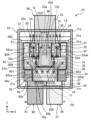
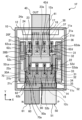
- FIG. 3A schematically shows a plan view of essential parts of an example of a semiconductor device.
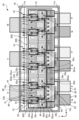
- FIG. 3(B) schematically shows a cross-sectional view taken along line III--III in FIG. 3(A).
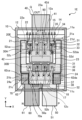
- FIG. 4 schematically shows a plan view of essential parts of an example of a case of a semiconductor device, an insulated circuit board, etc.
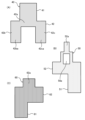
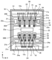
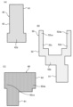
- FIG. 5A schematically shows a plan view of essential parts of an example of an OUT terminal of a semiconductor device.
- FIG. 5B schematically shows a plan view of a main part of an example of a P terminal of a semiconductor device.
- FIG. 5C schematically shows a plan view of essential parts of an example of an N terminal of a semiconductor device.
- the semiconductor device 1A shown in FIGS. 3(A) and 3(B) is an example of a so-called 2-in-1 type semiconductor device having a circuit configuration as shown in FIG. 1 above.
- the semiconductor device 1A includes a case 10, an insulating circuit board 20A, a plurality of semiconductor elements 30A, and a plurality of semiconductor elements 30B as shown in FIGS. 3A, 3B, and 4.
- the semiconductor device 1A further includes an OUT terminal 40, a P terminal 50, and an N terminal 60 as shown in FIGS. 3(A) and 3(B) and FIGS. 5(A) to 5(C).
- the OUT terminal 40, P terminal 50, and N terminal 60 are also respectively referred to as main current wiring.
- a resin case formed using a resin material such as PPS (Poly-Phenylene-Sulfide) resin is used.
- the case 10 has a side wall 12 surrounding the inside.
- the case 10 may have a lid part that covers the inside surrounded by the side wall part 12.
- the case 10 is placed on a support 100 such as a heat sink or a cooler, for example.
- An insulated circuit board 20A is arranged inside the case 10.
- a plurality of semiconductor elements 30A and a plurality of semiconductor elements 30B are mounted on the insulated circuit board 20A.
- the insulated circuit board 20A includes an insulated substrate 21 (substrate), a conductive plate 22, a conductive plate 23, and a conductive plate 24 provided on one surface (main surface) of the insulated substrate 21, and one surface of the insulated substrate 21. It has a conductive plate 25 provided on the other surface (principal surface) on the opposite side.
- As the insulating substrate 21 a substrate made of alumina, composite ceramics containing alumina as a main component, aluminum nitride, silicon nitride, or the like is used.
- a conductive material such as copper is used for the conductive plates 22, 23, 24, and 25.
- a DCB (Direct Copper Bonding) board is used as the insulated circuit board 20A.
- Other substrates such as an AMB (Active Metal Brazed) substrate may be used as the insulated circuit board 20A.
- a group of semiconductor elements 30A and a group of semiconductor elements 30B are mounted on one side of the insulating substrate 21. Switch elements such as IGBTs and MOSFETs are used in the semiconductor element 30A group and the semiconductor element 30B group, respectively. Diode elements such as FWDs and SBDs are integrated in the semiconductor element 30A group and the semiconductor element 30B group, respectively.
- the insulating substrate 21 of the insulated circuit board 20A has four sides 21a (first side), side 21b (second side), side 21c (third side), and side 21d (fourth side) in plan view. Side 21a and side 21c are opposite to each other, and side 21b and side 21d are opposite to each other.
- the case 10 has a side 11a (fifth side) and a side 11c (sixth side) that sandwich sides 21a and 21c of the insulating substrate 21 in plan view and are parallel to the sides 21a and 21c.
- the side 11a of the case 10 is on the side 21a of the insulating substrate 21, and the side 11c of the case 10 is on the side 21c of the insulating substrate 21.
- the conductive plate 22 provided on one surface of the insulating substrate 21 , the conductive plate 23 and the conductive plate 24 are arranged side by side in the Y direction in plan view.
- the conductive plate 24, the conductive plate 23, and the conductive plate 22 are arranged side by side in the order of the conductive plate 24 toward the Y direction.
- the conductive plate 22, the conductive plate 23, and the conductive plate 24 are arranged such that, for example, the area of the conductive plate 23 is larger than the area of the conductive plate 22, and the area of the conductive plate 22 is larger than the area of the conductive plate 24. .
- a plurality of (here, four as an example) semiconductor elements 30A forming the upper arm of the semiconductor device 1A are arranged on the conductive plate 22.
- the semiconductor elements 30A group of the upper arm on the conductive plate 22 are arranged side by side in the X direction in plan view.
- a plurality of (here, four as an example) semiconductor elements 30B forming the lower arm of the semiconductor device 1A are arranged on the conductive plate 23.
- the semiconductor elements 30B group of the lower arm on the conductive plate 23 are arranged side by side in the X direction in plan view.
- Each of the semiconductor element 30A group and the semiconductor element 30B group includes a collector electrode 31 provided on one surface (principal surface), and an emitter electrode 32 provided on the other surface (principal surface) opposite to the one surface.
- a collector electrode 31 provided on one surface (principal surface)
- an emitter electrode 32 provided on the other surface (principal surface) opposite to the one surface.
- a gate electrode and a sense emitter electrode are further provided on the side where the emitter electrode 32 is provided.
- a collector electrode 31 is connected to the conductive plate 22 using a bonding material such as solder or sintered material, and an emitter electrode 32 is connected to the conductive plate 23 using a wire 33.
- a collector electrode 31 is electrically connected to the conductive plate 22, and an emitter electrode 32 is electrically connected to the conductive plate 23.
- the gate electrode of each semiconductor element 30A on the upper arm is connected to an external gate terminal 14 provided on the side wall 12 of the case 10 on the side 11a side using a gate wire 34.
- the sense emitter electrode of each semiconductor element 30A of the upper arm is connected to an external sense emitter terminal 15 provided on the side wall 12 of the case 10 on the side 11a side using a sense emitter wire 35. Further, the conductive plate 22 to which the collector electrode 31 of each semiconductor element 30A of the upper arm is connected is connected to the external SP terminal 19 provided on the side wall 12 on the side 11a side of the case 10 using an SP wire 39. Ru. Below, these external SP terminals 19 and SP wires 39 are also referred to as SP section 90.
- a collector electrode 31 is connected to the conductive plate 23 using a bonding material such as solder or sintered material, and an emitter electrode 32 is connected to the conductive plate 24 using a wire 36.
- a collector electrode 31 is electrically connected to the conductive plate 23, and an emitter electrode 32 is electrically connected to the conductive plate 24.
- the gate electrode of each semiconductor element 30B of the lower arm is connected to an external gate terminal 17 provided on the side wall portion 12 of the case 10 on the side 11c side using a gate wire 37.
- the sense emitter electrode of each semiconductor element 30B of the lower arm is connected to an external sense emitter terminal 18 provided on the side wall 12 of the case 10 on the side 11c side using a sense emitter wire 38.
- a conductive block 22a (drawing part) to which the P terminal 50 (main current wiring) is connected is arranged.
- a conductive material such as copper is used for the conductive block 22a.
- the conductive block 22a is arranged at an intermediate position between the group of semiconductor elements 30A on the upper arm, that is, at a position sandwiched between the second and third of the four semiconductor elements 30A lined up in the X direction.
- the P terminal 50 is connected to the conductive block 22a and electrically connected to the conductive plate 22 via the conductive block 22a.
- the conductive plate 23 On the conductive plate 23 to which the emitter electrode 32 of the semiconductor element 30A group on the upper arm and the collector electrode 31 of the semiconductor element 30B group on the lower arm are connected, there are two conductive blocks to which the OUT terminal 40 (main current wiring) is connected. 23a (drawer part) is arranged. A conductive material such as copper is used for the conductive block 23a.
- the two conductive blocks 23a are located outside the joint group of wires 33 extending from the emitter electrode 32 of the semiconductor element 30A group on the upper arm and the semiconductor element 30B group on the lower arm, that is, the four semiconductor elements 30B lined up in the X direction. It is placed between the groups.
- the OUT terminal 40 is connected to a conductive block 23a and electrically connected to the conductive plate 23 via the conductive block 23a.
- a conductive block 24a (drawing part) to which the N terminal 60 (main current wiring) is connected is arranged on the conductive plate 24 to which the emitter electrodes 32 of the group of semiconductor elements 30B of the lower arm are connected.
- a conductive material such as copper is used for the conductive block 24a.
- the conductive block 24a is sandwiched between the joint groups of the wires 36 extending from the emitter electrodes 32 of the semiconductor elements 30B group of the lower arm, that is, between the second and third joint groups arranged in the X direction. placed in position.
- the N terminal 60 is connected to the conductive block 24a and electrically connected to the conductive plate 24 via the conductive block 24a.
- the conductive block 22a sandwiched between the semiconductor elements 30A group of the upper arm and the two conductive blocks 23a sandwiched between the semiconductor elements 30B group of the lower arm are arranged so that the length in the Y direction is longer than the length in the X direction when viewed from above. Shape.
- the conductive block 24a sandwiched between the joints of the wires 36 extending from the group of semiconductor elements 30B of the lower arm is set so that the length in the X direction is longer than the length in the Y direction in plan view. This prevents the semiconductor device 1A (its insulated circuit board 20A and case 10) from increasing in size in the X and Y directions due to the arrangement of the conductive blocks 22a and 23a.
- the two conductive blocks 23a to which the OUT terminal 40 is connected have a total plane size (area) larger than the plane size (area) of the conductive block 22a to which the P terminal 50 is connected, for example, ⁇ 2 times.
- the shape is as described above.
- the two conductive blocks 23a to which the OUT terminal 40 is connected have a total planar size (area) larger than the planar size (area) of the conductive block 24a to which the N terminal 60 is connected, for example, ⁇ 2 times.
- the shape is as described above. This is because the main current flowing through the OUT terminal 40 is theoretically ⁇ 2 times larger than the main currents flowing through the P terminal 50 and the N terminal 60.
- the total planar size of the two conductive blocks 23a to which the OUT terminal 40 is connected is the same as or smaller than the planar size of each of the conductive blocks 22a and 24a to which the P terminal 50 and N terminal 60 are connected.
- the current density increases, and there are concerns about heat generation and migration at the joint between the OUT terminal 40 and the conductive block 23a.
- the case 10 includes an insulated circuit board 20A including the conductive plates 22, 23, and 24 on which the upper arm semiconductor elements 30A group and the lower arm semiconductor element 30B group are mounted and connected as described above. .
- An OUT terminal 40, a P terminal 50, and an N terminal 60 are connected to an insulated circuit board 20A included in the case 10.
- the OUT terminal 40 has an external terminal part 41 arranged outside the case 10 and an extension part 42 arranged inside the case 10, as shown in FIGS. 3(A) and 5(A).
- the external terminal section 41 is provided on one side 11a of the case 10.
- the extending portion 42 is continuous with the external terminal portion 41 and extends from one side 11a of the case 10 to the inside of the case 10.
- the OUT terminal 40 is arranged so as to pass through an opening 12a provided in the side wall 12 on one side 11a of the case 10.
- the extending portion 42 includes a trunk 42a extending from one side 11a of the case 10 toward the inside of the case 10, and a branch 42b and a branch 42c branched from the trunk 42a in plan view.
- the branching portion 42b and the branching portion 42c are connected to two conductive blocks 23a arranged on the conductive plate 23 to which the collector electrodes 31 of the group of semiconductor elements 30B of the lower arm are connected, through a connecting portion 42ba and a connecting portion 42ca, respectively.
- Ru The extending portion 42 connects the external terminal portion 41 and the connecting portions 42ba and 42ca of the two conductive blocks 23a of the branching portion 42b and the branching portion 42c to each other.
- the OUT terminal 40 is electrically connected to the conductive plate 23 via the connecting portion 42ba, the connecting portion 42ca, and the two conductive blocks 23a.
- the P terminal 50 has an external terminal portion 51 disposed outside the case 10 and an extension portion 52 disposed inside the case 10.
- the external terminal portion 51 is provided on the other side 11c of the case 10.
- the extending portion 52 is continuous with the external terminal portion 51 and extends from the other side 11c of the case 10 to the inside of the case 10.
- the P terminal 50 is arranged so as to pass through an opening 12c provided in the side wall 12 on the other side 11c of the case 10.
- the extending portion 52 is connected at a connecting portion 52a to a conductive block 22a disposed on the conductive plate 22 to which the collector electrode 31 of the semiconductor element 30A group of the upper arm is connected.
- the extending portion 52 connects the external terminal portion 51 and the connecting portion 52a with the conductive block 22a to each other.
- the P terminal 50 is electrically connected to the conductive plate 22 via the connecting portion 52a and the conductive block 22a.
- the N terminal 60 includes an external terminal portion 61 disposed outside the case 10 and an extension portion 62 disposed inside the case 10.
- the external terminal portion 61 is provided on the other side 11c of the case 10.
- the extending portion 62 is continuous with the external terminal portion 61 and extends from the other side 11c of the case 10 to the inside of the case 10.
- the N terminal 60 and the P terminal 50 are arranged to pass through an opening 12c provided in the side wall 12 on the other side 11c of the case 10.
- the extension portion 62 is connected at a connecting portion 62a to a conductive block 24a arranged on the conductive plate 24 to which the emitter electrode 32 of the group of semiconductor elements 30B of the lower arm is connected.
- the extending portion 62 connects the external terminal portion 61 and the connecting portion 62a with the conductive block 24a to each other.
- the N terminal 60 is electrically connected to the conductive plate 24 via the connecting portion 62a and the conductive block 24a.
- the P terminal 50 and the N terminal 60 are stacked at least inside the case 10 with an insulating member 70 in between.
- an insulating sheet, insulating paper, or the like is used for the insulating member 70.
- a resin material such as aramid resin, polyamide resin, fluororesin, or polyimide resin is used for the insulating member 70.
- the N terminal 60, the insulating member 70, and the P terminal 50 are arranged in this order in the direction away from the insulating circuit board 20A. That is, of the P terminal 50 and the N terminal 60, the N terminal 60 is arranged closer to the insulated circuit board 20A.
- the P terminal 50 and the N terminal 60 have shapes that partially overlap in plan view.
- the N terminal 60 is not provided below the connection portion 52a of the P terminal 50.
- the P terminal 50 and the insulating member 70 are provided with an opening 50a and an opening 70a, respectively.
- the connecting portion 62a of the N terminal 60 is exposed through the opening 50a of the P terminal 50 and the opening 70a of the insulating member 70.
- a connecting portion 62a of the N terminal 60 is provided below the opening 50a of the P terminal 50 and the opening 70a of the insulating member 70.
- the connecting portion 62a of the N terminal 60 is joined to the conductive block 24a by laser welding or the like through the opening 50a of the P terminal 50 and the opening 70a of the insulating member 70.
- the extending portion 52 of the P terminal 50 and the extending portion 62 of the N terminal 60 are branched from the side 11c of the case 10 at the extending portion 42 of the OUT terminal 40. It extends between the portion 42b and the branch portion 42c.
- the connecting portions 42ba and 42ca of the branching portions 42b and 42c of the OUT terminal 40 which are connected to the two conductive blocks 23a, are the extending portion 52 of the P terminal 50 and the extending portion 62 of the N terminal 60. are placed between them.
- the group of semiconductor elements 30B of the lower arm is arranged between the branch part 42b and the branch part 42c of the OUT terminal 40.
- a sealing resin 110 may be provided for sealing the insulated circuit board 20A, the semiconductor element 30A group, the semiconductor element 30B group, etc. mounted thereon. .
- a resin material such as epoxy resin or phenol resin, or a gel material such as silicone is used.
- the sealing resin 110 may contain an insulating filler such as silica.
- Multiple types of materials may be used for the sealing resin 110, for example, a laminated structure in which a gel material such as silicone is provided as a buffer coating material in the lower layer and a resin material such as epoxy resin is provided in the upper layer. You can also.
- FIG. 6 and 7 are diagrams illustrating the flow of the main current during operation of the semiconductor device according to the first embodiment.
- FIG. 6 schematically shows a plan view of essential parts of an example of a semiconductor device.
- FIG. 7A schematically shows a plan view of essential parts of an example of a semiconductor device.
- FIG. 7(B) schematically shows a VII-VII cross-sectional view of FIG. 7(A).
- FIG. 6 schematically shows a plan view of essential parts of an example of a semiconductor device.
- FIG. 7(B) schematically shows a VII-VII cross-sectional view of FIG. 7(A).
- FIG. 6 FIG. 7(A), and FIG. 7(B)
- the flow of the main current during operation is schematically shown by thick arrows.
- a high potential power supply voltage is input to the P terminal 50, and a low potential power supply voltage is input to the N terminal 60.
- the main current entering from the P terminal 50 flows to the OUT terminal 40 through a route as shown in FIG. That is, the main current that enters from the external terminal portion 51 of the P terminal 50 flows through the extension portion 52, flows from the connecting portion 52a to the conductive plate 22 of the insulated circuit board 20A through the conductive block 22a, and flows to the conductive plate 22 of the insulated circuit board 20A, and the main current flows through the extension portion 52. It is supplied to the collector electrode 31.
- the main current supplied to the collector electrode 31 flows through the group of semiconductor elements 30A of the upper arm controlled through the gate wire 34, and flows to the conductive plate 23 of the insulated circuit board 20A through the emitter electrode 32 and the wire 33 connected thereto. .
- the main current flowing through the conductive plate 23 flows from the two conductive blocks 23a through the connecting portions 42ba and 42ca of the OUT terminal 40 to the branch portions 42b and 42c of the extension portion 42 and the trunk 42a, and flows to the external terminal portion. 41 (output current).
- the main current that enters from the OUT terminal 40 flows to the N terminal 60 through a route as shown in FIG. That is, the main current that enters from the external terminal portion 41 of the OUT terminal 40 flows to the trunk 42a, branch portions 42b and 42c of the extension portion 42, and flows from the connection portion 42ba and the connection portion 42ca to the insulated circuit board through the two conductive blocks 23a. It flows to the conductive plate 23 of 20A and is supplied to the collector electrode 31 of the group of semiconductor elements 30B of the lower arm.
- the main current supplied to the collector electrode 31 passes through the group of semiconductor elements 30B in the lower arm, which is controlled through the gate wire 37, and flows to the conductive plate 24 of the insulated circuit board 20A through the emitter electrode 32 and the wire 36 connected thereto. .
- the main current that has flowed through the conductive plate 24 flows from the conductive block 24 a through the connecting portion 62 a of the N terminal 60 to the extension portion 62 and then to the external terminal portion 61 .
- two conductive blocks 23a are connected to the connecting portion 42ba and the connecting portion 42ca of the OUT terminal 40, respectively, on the outside of the group of semiconductor elements 30B of the lower arm on the conductive plate 23, that is, so as to sandwich them. Placed.
- the main current flowing from the P terminal 50 to the OUT terminal 40 via the group of semiconductor elements 30A in the upper arm is prevented from flowing under the group of semiconductor elements 30B in the lower arm.
- the main current flowing from the P terminal to the OUT terminal via the semiconductor element group of the upper arm and the OUT terminal A structure may be adopted in which both the main current flowing from the main current to the N terminal via the semiconductor element group of the lower arm flow under the semiconductor element group of the lower arm.
- the main current flows from the P terminal 50 to the OUT terminal 40 via the group of semiconductor elements 30A on the upper arm, and from the OUT terminal 40 via the group of semiconductor elements 30B on the lower arm to the N terminal.
- Both the main current flowing through the main current 60 and the main current 60 are suppressed from flowing under the group of semiconductor elements 30B in the lower arm.
- two conductive blocks 23a to which the OUT terminal 40 is connected are arranged on the conductive plate 23, and the total planar size of the two conductive blocks 23a is the conductive block to which the P terminal 50 is connected.
- a structure is adopted in which the planar size of the conductive block 22a is larger than the planar size of the conductive block 24a to which the N terminal 60 is connected.
- the P terminal 50 (extended portion 52 thereof) and the N terminal 60 (extended portion 62 thereof) are stacked with the insulating member 70 in between so as to partially overlap in plan view.
- the path of the main current flowing between the P terminal 50 and the N terminal 60 is a relatively short closed loop, and the insulating member 70
- the inductance is reduced by magnetic flux cancellation between the P terminal 50 and the N terminal 60 which face each other via the inductance.
- voltage jumps caused by switching of the semiconductor element 30A group and the semiconductor element 30B group are suppressed, and performance deterioration of the semiconductor device 1A is suppressed.
- the semiconductor device 1A in order to make the main current path between the P terminal 50 and the N terminal 60 into a closed loop, it is not necessary to separately arrange a pattern (conductive plate) on the insulated circuit board 20A. Therefore, high packaging density of the insulated circuit board 20A and the group of semiconductor elements 30A and the group of semiconductor elements 30B mounted thereon is realized, and the enlargement of the semiconductor device 1A due to the increase in the size of the insulated circuit board 20A is suppressed. In the semiconductor device 1A, the main current path between the P terminal 50 and the N terminal 60 can be closed in a relatively short distance, so that the effect of reducing inductance is further enhanced.
- the N terminal 60 is arranged on the insulated circuit board 20A side (FIGS. 3(A) and 3(B) )).
- the N terminal 60 (its extension portion 62) is arranged to face the gate wire 37 and sense emitter wire 38 connected to the group of semiconductor elements 30B in the lower arm on the insulated circuit board 20A. That is, in the semiconductor device 1A, the N terminal 60 connected to the low potential side of the group of semiconductor elements 30B in the lower arm is connected to the gate wire 37 of the group of semiconductor elements 30B in the lower arm and the low potential side of the group of semiconductor elements 30B in the lower arm.
- the N terminal 60 can be arranged closer to the gate wire 37 and the sense emitter wire 38.
- the OUT terminal 40 (its extension portion 42) is arranged to face the gate wire 34 and the sense emitter wire 35 connected to the semiconductor element 30A group on the upper arm on the insulated circuit board 20A. (Fig. 3(A) and Fig. 3(B)). That is, in the semiconductor device 1A, the OUT terminal 40 connected to the low potential side of the semiconductor element 30A group on the upper arm is connected to the gate wire 34 of the semiconductor element 30A group on the upper arm and the low potential side of the semiconductor element 30A group on the upper arm. It faces the sense emitter wire 35 connected to the side. In this case, the potential difference between the OUT terminal 40, the gate wire 34, and the sense emitter wire 35 is relatively small. Therefore, it becomes possible to arrange the OUT terminal 40 close to the gate wire 34 and the sense emitter wire 35.
- the semiconductor device 1A it is possible to arrange the N terminal 60 close to the gate wire 37 and the sense emitter wire 38 and the OUT terminal 40 close to the gate wire 34 and the sense emitter wire 35. Therefore, it is possible to reduce the height of the semiconductor device 1A.
- an SP section 90 electrically connected to the conductive plate 22 is arranged as in the semiconductor device 1A, the external SP terminal 19 and the SP wire 39 of the SP section 90 are arranged opposite to the SP section 90.
- An insulating member such as an insulating sheet may be placed between the OUT terminal 40 and the OUT terminal 40, for example, between the SP section 90 in the area Q shown in FIGS. 3A and 4 and the OUT terminal 40.
- a portion of the OUT terminal 40 facing the external SP terminal 19 and the SP wire 39 of the SP section 90 for example, a portion of the OUT terminal 40 in the area Q shown in FIGS. May be removed.
- the relationship between the semiconductor device 1A and the elements recited in claim 1 is as follows.
- the OUT terminal 40 corresponds to the "first main current wiring”
- the trunk 42a corresponds to the "trunk”
- the branch part 42b and the branch part 42c correspond to the "first branch part and the second branch part”
- the extension part 42 corresponds to the "first branch part”. 1 stretching section, respectively.
- the P terminal 50 or the N terminal 60 corresponds to the "second main current wiring".
- the extension part 52 corresponds to the "second extension part”
- the conductive plate 22 to which it is electrically connected is the "conductive plate”.
- the group of semiconductor elements 30A on the upper arm corresponds to "a plurality of semiconductor elements”
- the collector electrode 31 of the group of semiconductor elements 30A on the upper arm, which is electrically connected to the conductive plate 22, corresponds to the "first electrode”.
- the emitter electrode 32 of the group of semiconductor elements 30A on the upper arm corresponds to the "second electrode”.
- the extension part 62 corresponds to the "second extension part”
- the conductive plate 24 to which it is electrically connected is the "conductive plate”.
- the group of semiconductor elements 30B in the lower arm corresponds to "a plurality of semiconductor elements”
- the emitter electrode 32 of the group of semiconductor elements 30B in the lower arm electrically connected to the conductive plate 24 corresponds to "the first electrode”.
- the collector electrode 31 of the group of semiconductor elements 30B on the lower arm corresponds to the "second electrode”.
- the OUT terminal 40 corresponds to the "first main current wiring”
- the external terminal section 41 corresponds to the "first external terminal section”
- the extension section 42 corresponds to the "first extension section”
- the connection section 42ba and connection section 42ca correspond to "the first extension section”.
- “first connection part” and “second connection part” respectively.
- the P terminal 50 or the N terminal 60 corresponds to the "second main current wiring”.
- the P terminal 50 is the "second main current wiring”
- the external terminal part 51 corresponds to the "second external terminal part”
- the extension part 52 corresponds to the "second extension part”
- the connecting part 52a corresponds to a "third connecting part”
- the conductive plate 23 corresponds to a "first conductive plate”
- the conductive plate 22 corresponds to a "second conductive plate”
- the semiconductor elements 30B group of the lower arm correspond to This corresponds to "a plurality of first semiconductor elements”
- the group of semiconductor elements 30A on the upper arm corresponds to "a plurality of second semiconductor elements.”
- the extending portion 62 is a “third extending portion”
- the connecting portion 62a is a “fourth connecting portion”
- the conductive plate 24 is a “third conductive plate”
- the wire 36 is a “first wire”
- the wire 33 is a “second wire”.
- the opening 12a is the “first opening” and the opening 12c is the “second opening” (Claim 18).
- the insulating member 70 becomes an “insulating member” (claim 19), the opening 50a and the opening 70a become a “third opening” and a “fourth opening”, respectively, and the conductive block 24a becomes a “conductive block” (claim 19).
- Gate wire 37 is “first gate wire”
- sense emitter wire 38 is “first sense emitter wire”
- gate wire 34 is “second gate wire”
- sense emitter wire 35 is “second sense emitter wire”
- the terminal 17 is the “first external gate terminal”
- the external sense emitter terminal 18 is the “first external sense emitter terminal”
- the external gate terminal 14 is the “second external gate terminal”
- the external sense emitter terminal 15 is the "second external sense terminal”.
- “emitter terminal” (Claim 21).
- the N terminal 60 is the "second main current wiring”
- the external terminal part 61 corresponds to the "second external terminal part”
- the extension part 62 corresponds to the "second extension part”
- the connection The portion 62a corresponds to a “third connection portion”
- the conductive plate 23 corresponds to a “first conductive plate”
- the conductive plate 24 corresponds to a “second conductive plate”
- the group of semiconductor elements 30A of the upper arm corresponds to a “first conductive plate.”
- the group of semiconductor elements 30B on the lower arm corresponds to "a plurality of second semiconductor elements”.
- the external terminal portion 51 of the P terminal 50 and the external terminal portion 61 of the N terminal 60 arranged outside the case 10 are made of an insulating member in a plan view. may be arranged so as to overlap through the .
- the P terminal 50 and the N terminal 60 can also be changed to a shape such that the external terminal portions 51 and 61 are arranged overlapping each other with an insulating member interposed therebetween in a plan view.
- FIG. 2 a three-phase voltage source inverter circuit (FIG. 2) of U phase, V phase, and W phase by using three semiconductor devices 1A as described in the first embodiment.
- the semiconductor device 1A is packaged in a 2-in-1 package, but when configuring a three-phase voltage source inverter circuit, the functional parts of each phase, U-phase, V-phase, and W-phase, are housed in one case. , it can also be a 6in1 package.
- FIG. 8 to 10 are diagrams illustrating an example of a semiconductor device according to the second embodiment.
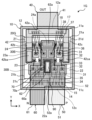
- FIG. 8 schematically shows a plan view of essential parts of an example of a semiconductor device.
- FIG. 9 schematically shows a plan view of essential parts of an example of a case of a semiconductor device, an insulated circuit board, etc.
- FIG. 10A schematically shows a plan view of essential parts of an example of an OUT terminal of a semiconductor device.
- FIG. 10B schematically shows a plan view of a main part of an example of a P terminal of a semiconductor device.
- FIG. 10C schematically shows a plan view of essential parts of an example of an N terminal of a semiconductor device.
- a semiconductor device 1B shown in FIG. 8 is an example of a so-called 2-in-1 type semiconductor device having a circuit configuration as shown in FIG. 1 above.
- the semiconductor device 1B includes a case 10 as shown in FIGS. 8 and 9, an insulated circuit board 20B, and a plurality of semiconductor elements 30A and a plurality of semiconductor elements 30B.
- the semiconductor device 1B further includes an OUT terminal 40, a P terminal 50, and an N terminal 60 as shown in FIGS. 8 and 10(A) to 10(C).
- the OUT terminal 40, P terminal 50, and N terminal 60 are also respectively referred to as main current wiring.
- an insulated circuit board 20B on which a group of semiconductor elements 30A of the upper arm and a group of semiconductor elements 30B of the lower arm are mounted is arranged.
- the insulated circuit board 20B includes two conductive plates 23A and 23A on which, for example, four groups of lower arm semiconductor elements 30B are arranged, for example, two each, on an insulating substrate 21 (substrate). It has a conductive plate 23B.
- a conductive block 23a to which the branch portion 42b and the branch portion 42c of the OUT terminal 40 are respectively joined is arranged on each of the conductive plates 23A and 23B.
- a conductive block 22a and a conductive block 24a are respectively disposed on a portion of the conductive plate 22 and a portion of the conductive plate 24 extending in the area between the conductive plates 23A and 23B.
- the total area of the conductive plate 23A and the conductive plate 23B is larger than the area of the conductive plate 22, and the area of the conductive plate 22 is larger than the area of the conductive plate 24. It is arranged so that it is larger than the area.
- the total planar size of the two conductive blocks 23a on the conductive plate 23A and the conductive plate 23B is It is set to be larger than the planar size of the conductive block 22a on the plate 22 and larger than the planar size of the conductive block 24a on the conductive plate 24. Furthermore, in order to suppress the increase in size of the semiconductor device 1B (its insulated circuit board 20B and case 10), each of the two conductive blocks 23a is arranged between the semiconductor element 30B of the lower arm and the semiconductor element 30A of the upper arm in the Y direction.
- the insulated circuit board 20B of the semiconductor device 1B is different from the insulated circuit board 20A of the semiconductor device 1A described in the first embodiment in that it has such a configuration.
- the group of semiconductor elements 30A of the upper arm is arranged on the conductive plate 22, the collector electrode 31 is connected to the conductive plate 22, and the emitter electrode 32 is connected by a wire 33 to the conductive plate 23A and the conductive plate 23B.
- a gate wire 34 and a sense emitter wire 35 are connected to the group of semiconductor elements 30A on the upper arm, and are connected to an external gate terminal 14 and an external sense emitter terminal 15, respectively.
- the semiconductor elements 30B of the lower arm are arranged, for example, two each on the conductive plate 23A and the conductive plate 23B, the collector electrode 31 is connected to the conductive plate 23A and the conductive plate 23B, and the emitter electrode 32 is connected to the wire 36. and is connected to the conductive plate 24.
- a gate wire 37 and a sense emitter wire 38 are connected to the group of semiconductor elements 30B in the lower arm, and are connected to an external gate terminal 17 and an external sense emitter terminal 18, respectively. Further, the SP section 90 (external SP terminal 19 and SP wire 39 described in the first embodiment) is connected to the conductive plate 22 to which the collector electrode 31 of the semiconductor element group 30A of the upper arm is connected. .
- the OUT terminal 40 includes an external terminal portion 41 disposed outside the case 10 and an extension portion 42 disposed inside the case 10. is arranged so as to pass through an opening 12a provided in the side wall portion 12 on one side 11a side.
- Branch portions 42b and 42c of the OUT terminal 40 branched from the trunk 42a of the extension portion 42 are connected to the two conductive blocks 23a at respective connection portions 42ba and 42ca, respectively.
- the OUT terminal 40 is electrically connected to the conductive plate 23A and the conductive plate 23B via the connecting portion 42ba, the connecting portion 42ca, and the two conductive blocks 23a.
- the P terminal 50 includes an external terminal portion 51 disposed outside the case 10 and an extension portion 52 disposed inside the case 10. It is arranged so as to pass through an opening 12c provided in the side wall portion 12 on the other side 11c side.
- the extending portion 52 is connected to the conductive block 22a on the conductive plate 22 at a connecting portion 52a.
- the P terminal 50 is electrically connected to the conductive plate 22 via the connecting portion 52a and the conductive block 22a.
- the N terminal 60 has an external terminal portion 61 disposed outside the case 10 and an extension portion 62 disposed inside the case 10.
- the P terminal 50 is arranged so as to pass through an opening 12c provided in the side wall portion 12 on the other side 11c side.
- the extending portion 62 is connected to the conductive block 24a on the conductive plate 24 at a connecting portion 62a.
- the N terminal 60 is electrically connected to the conductive plate 24 via the connecting portion 62a and the conductive block 24a.
- the P terminal 50 and the N terminal 60 are stacked at least inside the case 10 with an insulating member 70 such as an insulating sheet interposed therebetween.
- the N terminal 60, the insulating member 70, and the P terminal 50 are arranged in this order in the direction away from the insulated circuit board 20B.
- the P terminal 50 and the N terminal 60 have shapes that partially overlap in plan view.
- the N terminal 60 is not provided below the connection portion 52a of the P terminal 50.
- the connecting portion 62a of the N terminal 60 is exposed through the opening 50a of the P terminal 50 and the opening 70a of the insulating member 70.
- the connecting portion 62a of the N terminal 60 is joined to the conductive block 24a by laser welding or the like through the opening 50a of the P terminal 50 and the opening 70a of the insulating member 70.
- the extending portion 52 of the P terminal 50 and the extending portion 62 of the N terminal 60 are located between the branching portion 42b and the branching portion 42c of the OUT terminal 40 from the side 11c side of the case 10. It is extended to.
- the connecting portions 42ba and 42ca of the branching portions 42b and 42c of the OUT terminal 40 which are connected to the two conductive blocks 23a, are the extending portion 52 of the P terminal 50 and the extending portion 62 of the N terminal 60. are placed between them.
- the elements are arranged in the order of section 41.
- a sealing resin may be provided inside the case 10 to seal the insulated circuit board 20B, the semiconductor element 30A group, the semiconductor element 30B group, etc. mounted thereon, according to the example shown in FIG. 3(B). Note that in FIG. 8, illustration of the sealing resin is omitted for convenience.
- a high potential power supply voltage is input to the P terminal 50, and a low potential power supply voltage is input to the N terminal 60.
- the main current that enters from the external terminal section 51 of the P terminal 50 flows through the extension section 52, and from the connection section 52a thereof flows through the conductive block 22a to the conductive plate 22 of the insulated circuit board 20B, and the collector electrode of the group of semiconductor elements 30A on the upper arm. 31.
- the main current supplied to the collector electrode 31 passes through the group of semiconductor elements 30A of the upper arm, which is controlled through the gate wire 34, and passes through the emitter electrode 32 and the wire 33 connected thereto to the conductive plate 23A of the insulated circuit board 20B and the conductive plate 23A of the insulated circuit board 20B. It flows to plate 23B.
- the main current flowing through the conductive plates 23A and 23B flows from the two conductive blocks 23a to the branch portions 42b and 42c of the extension portion 42 and the trunk 42a through the connection portions 42ba and 42ca of the OUT terminal 40. , flows to the external terminal section 41.
- the main current that enters from the external terminal section 41 of the OUT terminal 40 flows to the trunk 42a, branch section 42b and branch section 42c of the extension section 42, and passes through the two conductive blocks 23a from the connection section 42ba and connection section 42ca to the insulated circuit board. It flows to the conductive plates 23A and 23B of 20B, and is supplied to the collector electrode 31 of the group of semiconductor elements 30B of the lower arm.
- the main current supplied to the collector electrode 31 passes through the lower arm group of semiconductor elements 30B controlled through the gate wire 37, and flows to the conductive plate 24 of the insulated circuit board 20B through the emitter electrode 32 and the wire 36 connected thereto. .
- the main current that has flowed through the conductive plate 24 flows from the conductive block 24 a through the connecting portion 62 a of the N terminal 60 to the extension portion 62 and then to the external terminal portion 61 .
- the OUT terminal 40 is connected to a region of the conductive plate 23A and the conductive plate 23B between the connection portion of the wire 33 extending from the semiconductor element group 30A of the upper arm and the semiconductor element group 30B of the lower arm.
- Two conductive blocks 23a are arranged.
- the main current flowing from the P terminal 50 to the OUT terminal 40 via the group of semiconductor elements 30A in the upper arm is prevented from flowing under the group of semiconductor elements 30B in the lower arm. Therefore, in the semiconductor device 1B, the main current flows from the P terminal 50 to the OUT terminal 40 via the group of semiconductor elements 30A on the upper arm, and from the OUT terminal 40 to the N terminal 60 via the group of semiconductor elements 30B on the lower arm.
- Both the flowing main current and the main current are prevented from passing under the group of semiconductor elements 30B in the lower arm. This suppresses performance deterioration due to overheating of the group of semiconductor elements 30B in the lower arm and performance deterioration of the semiconductor device 1B including them.
- the P terminal 50 (extended portion 52 thereof) and the N terminal 60 (extended portion 62 thereof) are stacked with the insulating member 70 in between so as to partially overlap in plan view.
- the path of the main current flowing between the P terminal 50 and the N terminal 60 is formed into a closed loop over a relatively short distance, and the path of the main current flowing between the P terminal 50 and the N terminal 60 facing each other via the insulating member 70 is formed into a closed loop.
- the inductance is reduced by magnetic flux cancellation. As a result, voltage jumps caused by switching of the semiconductor element 30A group and the semiconductor element 30B group are suppressed, and performance deterioration of the semiconductor device 1B is suppressed.
- the semiconductor device 1B in order to close the main current path between the P terminal 50 and the N terminal 60, it is not necessary to separately arrange a pattern (conductive plate) on the insulated circuit board 20B, so high packaging density can be achieved. is realized, and the enlargement of the semiconductor device 1B is suppressed.
- the N terminal 60 connected to the low potential side of the semiconductor element 30B group on the lower arm is connected to the gate wire 37 of the semiconductor element 30B group on the lower arm and the low potential side of the semiconductor element 30B group on the lower arm. It is opposed to the sense emitter wire 38 connected to the side. Therefore, it becomes possible to arrange the N terminal 60 relatively close to the gate wire 37 and the sense emitter wire 38.
- the OUT terminal 40 connected to the low potential side of the semiconductor element 30A group on the upper arm is connected to the gate wire 34 of the upper arm semiconductor element 30A group and the low potential side of the upper arm semiconductor element 30A group. It is opposed to the sense emitter wire 35 connected to the side.
- the OUT terminal 40 relatively close to the gate wire 34 and the sense emitter wire 35.
- the N terminal 60 is arranged close to the gate wire 37 and the sense emitter wire 38, and the OUT terminal 40 is arranged close to the gate wire 34 and the sense emitter wire 35, thereby reducing the height of the semiconductor device 1B. is realized.
- an SP section 90 electrically connected to the conductive plate 22 is arranged as in the semiconductor device 1B, between the SP section 90 and the OUT terminal 40, for example, a region Q shown in FIG.
- An insulating member such as an insulating sheet may be placed between the SP section 90 and the OUT terminal 40.
- a portion of the OUT terminal 40 facing the SP portion 90 for example, a portion of the OUT terminal 40 in the area Q shown in FIG. 8 may be partially removed. This suppresses the influence of the potential of the OUT terminal 40 placed close to the gate wire 34 and the sense emitter wire 35 on the potential of the SP section 90, making it possible to suppress destruction of the semiconductor device 1B due to overcurrent. Become.
- the relationship between the semiconductor device 1B and the elements recited in claims 1 and 10 is that the conductive plate 23 of the semiconductor device 1A described in the first embodiment is a semiconductor. In the device 1B, the relationship is similar to that described in the first embodiment, except that the conductive plates 23A and 23B are used.
- the conductive plate 23A and the conductive plate 23B of the semiconductor device 1B serve as a "first output conductive pattern" and a "second output conductive pattern" (Claim 22).
- the external terminal portion 51 of the P terminal 50 and the external terminal portion 61 of the N terminal 60 arranged outside the case 10 are made of an insulating member in a plan view. may be arranged so as to overlap through the .
- the P terminal 50 and the N terminal 60 can also be changed to a shape such that the external terminal portions 51 and 61 are arranged overlapping each other with an insulating member interposed therebetween in a plan view.
- FIG. 2 a three-phase voltage source inverter circuit (FIG. 2) of U phase, V phase, and W phase by using three semiconductor devices 1B as described in the second embodiment.
- the semiconductor device 1B is a 2-in-1 package, but when configuring a three-phase voltage source inverter circuit, the functional parts of each phase of U-phase, V-phase, and W-phase are housed in one case. , it can also be a 6in1 package.
- FIG. 11 to 13 are diagrams illustrating an example of a semiconductor device according to the third embodiment.
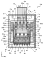
- FIG. 11 schematically shows a plan view of essential parts of an example of a semiconductor device.
- FIG. 12 schematically shows a plan view of essential parts of an example of a case of a semiconductor device, an insulated circuit board, etc.
- FIG. 13A schematically shows a plan view of essential parts of an example of an OUT terminal of a semiconductor device.
- FIG. 13B schematically shows a plan view of essential parts of an example of a P terminal of a semiconductor device.
- FIG. 13C schematically shows a plan view of essential parts of an example of an N terminal of a semiconductor device.
- a semiconductor device 1C shown in FIG. 11 is an example of a so-called 2-in-1 type semiconductor device having a circuit configuration as shown in FIG. 1 above.
- the semiconductor device 1C includes a case 10 as shown in FIGS. 11 and 12, an insulated circuit board 20C, and a plurality of semiconductor elements 30A and a plurality of semiconductor elements 30B.
- the semiconductor device 1C further includes an OUT terminal 40, a P terminal 50, and an N terminal 60 as shown in FIGS. 11 and 13(A) to 13(C).
- the OUT terminal 40, P terminal 50, and N terminal 60 are also respectively referred to as main current wiring.
- an insulated circuit board 20C on which a group of semiconductor elements 30A of the upper arm and a group of semiconductor elements 30B of the lower arm are mounted is arranged.
- the insulated circuit board 20C includes a conductive plate 22, a conductive plate 23, and a conductive plate 24 arranged on an insulating substrate 21 (substrate).
- the conductive plate 24, the conductive plate 23, and the conductive plate 22 are arranged in this order from the conductive plate 24 toward the Y direction.
- the conductive plate 22, the conductive plate 23, and the conductive plate 24 are arranged such that, for example, the area of the conductive plate 23 is larger than the area of the conductive plate 22, and the area of the conductive plate 22 is larger than the area of the conductive plate 24.
- a group of semiconductor elements 30A of the upper arm is arranged on the conductive plate 22, and a group of semiconductor elements 30B of the lower arm is arranged on the conductive plate 23.
- a collector electrode 31 is connected to the conductive plate 22, and an emitter electrode 32 is connected to the conductive plate 23 by a wire 33.
- a gate wire 34 and a sense emitter wire 35 are connected to the group of semiconductor elements 30A on the upper arm, and are connected to an external gate terminal 14 and an external sense emitter terminal 15, respectively.
- the collector electrode 31 is connected to the conductive plate 23, and the emitter electrode 32 is connected to the conductive plate 24 by a wire 36.
- a gate wire 37 and a sense emitter wire 38 are connected to the group of semiconductor elements 30B in the lower arm, and are connected to an external gate terminal 17 and an external sense emitter terminal 18, respectively.
- the SP section 90 (external SP terminal 19 and SP wire 39 described in the first embodiment) is connected to the conductive plate 22 to which the collector electrode 31 of the semiconductor element group 30A of the upper arm is connected. .
- Two conductive blocks 22a to which the P terminals 50 are connected are arranged on the conductive plate 22 to which the collector electrodes 31 of the group of semiconductor elements 30A of the upper arm are connected.
- the two conductive blocks 22a are arranged at positions outside the semiconductor element 30A group of the upper arm, that is, at positions sandwiching the four semiconductor element 30A groups lined up in the X direction.
- a conductive block 23a to which the OUT terminal 40 is connected is arranged on the conductive plate 23 to which the emitter electrodes 32 of the semiconductor elements 30A group of the upper arm and the collector electrodes 31 of the semiconductor elements 30B group of the lower arm are connected.
- the conductive block 23a is located at an intermediate position between the joint group of wires 33 extending from the emitter electrode 32 of the semiconductor element 30A group on the upper arm and the semiconductor element 30B group on the lower arm, that is, two of the four semiconductor elements 30B lined up in the X direction. It is placed between the 3rd and 3rd positions.
- Two conductive blocks 24a to which the N terminal 60 is connected are arranged on the conductive plate 24 to which the emitter electrodes 32 of the group of semiconductor elements 30B of the lower arm are connected.
- the two conductive blocks 24a are arranged at positions outside the group of joints of the wires 36 extending from the emitter electrodes 32 of the group of semiconductor elements 30B in the lower arm, that is, at positions sandwiching the group of joints arranged in the X direction.
- the block 24a is set in a predetermined shape in order to suppress the increase in size of the semiconductor device 1C (its insulated circuit board 20C and case 10). That is, the two conductive blocks 22a on the conductive plate 22 and the conductive block 23a on the conductive plate 23 are set so that the length in the Y direction is longer than the length in the X direction in plan view.
- the two conductive blocks 24a on the conductive plate 24 are set so that the length in the X direction is longer than the length in the Y direction in plan view.
- the planar size of the conductive block 23a on the conductive plate 23 is smaller than that of the two conductive blocks 22a on the conductive plate 22. is set to be larger than the sum of the plane sizes of the two conductive blocks 24a on the conductive plate 24, and larger than the sum of the plane sizes of the two conductive blocks 24a on the conductive plate 24.
- the OUT terminal 40 includes an external terminal portion 41 disposed outside the case 10 and an extension portion 42 disposed inside the case 10.
- the external terminal section 41 is provided on one side 11a of the case 10.
- the extending portion 42 is continuous with the external terminal portion 41 and extends from one side 11a of the case 10 to the inside of the case 10.
- the OUT terminal 40 is arranged so as to pass through an opening 12a provided in the side wall 12 on one side 11a of the case 10.
- the extending portion 42 is connected at a connecting portion 42d to a conductive block 23a arranged on the conductive plate 23 to which the collector electrode 31 of the group of semiconductor elements 30B of the lower arm is connected.
- the extending portion 42 connects the external terminal portion 41 and the connecting portion 42d to each other.
- the OUT terminal 40 is electrically connected to the conductive plate 23 via the connecting portion 42d and the conductive block 23a.
- the P terminal 50 has an external terminal portion 51 disposed outside the case 10 and an extension portion 52 disposed inside the case 10.
- the external terminal portion 51 is provided on the other side 11c of the case 10.
- the extending portion 52 is continuous with the external terminal portion 51 and extends from the other side 11c of the case 10 to the inside of the case 10.
- the P terminal 50 is arranged so as to pass through an opening 12c provided in the side wall 12 on the other side 11c of the case 10.
- the extending portion 52 includes a trunk 52b extending from the other side 11c of the case 10 toward the inside of the case 10, and a branching portion 52c and a branching portion 52d branching from the trunk 52b in plan view.
- the branching portion 52c and the branching portion 52d are connected to two conductive blocks 22a arranged on the conductive plate 22 to which the collector electrodes 31 of the group of semiconductor elements 30A of the upper arm are connected, through a connecting portion 52ca and a connecting portion 52da, respectively.
- Ru The extending portion 52 connects the external terminal portion 51 and a connecting portion 52ca and a connecting portion 52da between the two conductive blocks 22a, a branch portion 52c and a branch portion 52d.
- the P terminal 50 is electrically connected to the conductive plate 22 via the connecting portion 52ca, the connecting portion 52da, and the two conductive blocks 22a.
- the N terminal 60 has an external terminal portion 61 disposed outside the case 10 and an extension portion 62 disposed inside the case 10.
- the external terminal portion 61 is provided on the other side 11c of the case 10.
- the extending portion 62 is continuous with the external terminal portion 61 and extends from the other side 11c of the case 10 to the inside of the case 10.
- the N terminal 60 is arranged so as to pass through the opening 12c provided in the side wall 12 on the other side 11c side of the case 10 together with the P terminal 50.
- the extending portion 62 includes a trunk 62b extending from the other side 11c of the case 10 toward the inside of the case 10, and a branching portion 62c and a branching portion 62d branching from the trunk 62b in plan view.
- the branching portion 62c and the branching portion 62d are connected to two conductive blocks 24a arranged on the conductive plate 24 to which the emitter electrodes 32 of the group of semiconductor elements 30B of the lower arm are connected, through a connecting portion 62ca and a connecting portion 62da, respectively.
- Ru The extending portion 62 connects the external terminal portion 61 and the connecting portion 62ca and the connecting portion 62da between the two conductive blocks 24a of the branch portion 62c and the branch portion 62d.
- the N terminal 60 is electrically connected to the conductive plate 24 via the connecting portion 62ca, the connecting portion 62da, and the two conductive blocks 24a.
- the P terminal 50 and the N terminal 60 are stacked at least inside the case 10 with an insulating member 70 such as an insulating sheet interposed therebetween.
- the N terminal 60, the insulating member 70, and the P terminal 50 are arranged in this order in the direction away from the insulated circuit board 20C.
- the P terminal 50 and the N terminal 60 have shapes that partially overlap in plan view.
- the N terminal 60 is not provided below the connection portion 52ca and connection portion 52da of the P terminal 50.
- the P terminal 50 and the insulating member 70 are provided with an opening 50a and an opening 70a (notch), respectively.
- the connecting portion 62ca and the connecting portion 62da of the N terminal 60 are exposed through the opening 50a of the P terminal 50 and the opening 70a of the insulating member 70.
- a connecting portion 62ca and a connecting portion 62da of the N terminal 60 are provided below the opening 50a of the P terminal 50 and the opening 70a of the insulating member 70.
- the connecting portion 62ca and the connecting portion 62da of the N terminal 60 are joined to the two conductive blocks 24a by laser welding or the like through the opening 50a of the P terminal 50 and the opening 70a of the insulating member 70.
- the extending portion 42 of the OUT terminal 40 is located between the branching portion 52c and the branching portion 52d provided in the extending portion 52 of the P terminal 50, and between the extending portion 62 of the N terminal 60. It extends between the branch portion 62c and the branch portion 62d.
- the connecting portion 52ca and the connecting portion 52da of the branch portion 52c and the branch portion 52d of the P terminal 50, which are connected to the two conductive blocks 22a, are arranged so as to sandwich the extending portion 42 of the OUT terminal 40.
- the connecting portion 62ca and the connecting portion 62da of the branch portion 62c and the branch portion 62d of the N terminal 60, which are connected to the two conductive blocks 24a, are arranged so as to sandwich the extension portion 42 of the OUT terminal 40.
- the group of semiconductor elements 30A of the upper arm is arranged between the branch part 52c and the branch part 52d of the P terminal 50.
- a sealing resin may be provided inside the case 10 to seal the insulated circuit board 20C, the semiconductor element 30A group, the semiconductor element 30B group, etc. mounted thereon, according to the example shown in FIG. 3(B). Note that in FIG. 11, illustration of the sealing resin is omitted for convenience.
- a high potential power supply voltage is input to the P terminal 50, and a low potential power supply voltage is input to the N terminal 60.
- the main current that enters from the external terminal portion 51 of the P terminal 50 flows to the trunk 52b, branch portions 52c, and 52d of the extension portion 52, and flows from the connection portions 52ca and 52da to the two conductive blocks 22a to the insulated circuit board 20C. It flows to the conductive plate 22 and is supplied to the collector electrode 31 of the group of semiconductor elements 30A on the upper arm.
- the main current supplied to the collector electrode 31 passes through the group of semiconductor elements 30A in the upper arm, which is controlled through the gate wire 34, and flows to the conductive plate 23 of the insulated circuit board 20C through the emitter electrode 32 and the wire 33 connected thereto. .
- the main current that has flowed through the conductive plate 23 flows from the conductive block 23a to the extension portion 42 through the connection portion 42d of the OUT terminal 40, and then to the external terminal portion 41.
- the main current that enters from the external terminal section 41 of the OUT terminal 40 flows through the extension section 42, and flows from the connection section 42d to the conductive plate 23 of the insulated circuit board 20C through the conductive block 23a, and flows through the conductive plate 23 of the insulated circuit board 20C, and the main current flows through the extension section 42, and flows from the connecting section 42d to the conductive plate 23 of the insulated circuit board 20C, and flows through the conductive plate 23 of the insulated circuit board 20C. It is supplied to the collector electrode 31.
- the main current supplied to the collector electrode 31 passes through the group of semiconductor elements 30B in the lower arm controlled through the gate wire 37, and flows to the conductive plate 24 of the insulated circuit board 20C through the emitter electrode 32 and the wire 36 connected thereto. .
- the main current flowing through the conductive plate 24 flows from the two conductive blocks 24a through the connecting portions 62ca and 62da of the N terminal 60 to the branch portions 62c and 62d of the extension portion 62 and the trunk 62b, and flows to the external terminal portion. It flows to 61.
- the main current flowing from the P terminal 50 to the OUT terminal 40 via the group of semiconductor elements 30A in the upper arm is suppressed from flowing under the group of semiconductor elements 30B in the lower arm. Therefore, in the semiconductor device 1C, the main current flows from the P terminal 50 to the OUT terminal 40 via the group of semiconductor elements 30A on the upper arm, and from the OUT terminal 40 to the N terminal 60 via the group of semiconductor elements 30B on the lower arm. Both the flowing main current and the main current are prevented from passing under the group of semiconductor elements 30B in the lower arm. This suppresses performance deterioration due to overheating of the group of semiconductor elements 30B in the lower arm and performance deterioration of the semiconductor device 1C including them.
- the P terminal 50 (extended portion 52 thereof) and the N terminal 60 (extended portion 62 thereof) are stacked with the insulating member 70 in between so as to partially overlap in plan view.
- the path of the main current flowing between the P terminal 50 and the N terminal 60 is formed into a closed loop over a relatively short distance, and the path of the main current flowing between the P terminal 50 and the N terminal 60 facing each other via the insulating member 70 is formed into a closed loop.
- the inductance is reduced by magnetic flux cancellation. As a result, voltage jumps caused by switching of the semiconductor element 30A group and the semiconductor element 30B group are suppressed, and performance deterioration of the semiconductor device 1C is suppressed.
- the semiconductor device 1C in order to close the main current path between the P terminal 50 and the N terminal 60, it is not necessary to separately arrange a pattern (conductive plate) on the insulated circuit board 20C, so high packaging density can be achieved. is realized, and the enlargement of the semiconductor device 1C is suppressed.
- the N terminal 60 connected to the low potential side of the semiconductor element 30B group on the lower arm is connected to the gate wire 37 of the semiconductor element 30B group on the lower arm and the low potential side of the semiconductor element 30B group on the lower arm. It is opposed to the sense emitter wire 38 connected to the side.
- the OUT terminal 40 connected to the low potential side of the semiconductor element 30A group on the upper arm is connected to the gate wire 34 of the semiconductor element 30A group on the upper arm and the low potential side of the semiconductor element 30A group on the upper arm. It is opposed to the sense emitter wire 35 connected to the side.
- the N terminal 60 can be placed relatively close to the gate wire 37 and the sense emitter wire 38, and the OUT terminal 40 can be placed relatively close to the gate wire 34 and the sense emitter wire 35. A lower height is achieved.
- an SP section 90 electrically connected to the conductive plate 22 is arranged as in the semiconductor device 1C, between the SP section 90 and the OUT terminal 40, for example, a region Q shown in FIG.
- An insulating member such as an insulating sheet may be placed between the SP section 90 and the OUT terminal 40.
- a portion of the OUT terminal 40 facing the SP portion 90 for example, a portion of the OUT terminal 40 in the area Q shown in FIG. 11 may be partially removed. This suppresses the influence of the potential of the OUT terminal 40 placed close to the gate wire 34 and the sense emitter wire 35 on the potential of the SP section 90, making it possible to suppress destruction of the semiconductor device 1C due to overcurrent.
- the relationship between the semiconductor device 1C and the elements recited in claim 1 is as follows.
- the OUT terminal 40 corresponds to a "second main current wiring”
- the extending part 42 corresponds to a "second extending part”
- the conductive plate 23 corresponds to a "conductive plate.”
- the P terminal 50 or the N terminal 60 corresponds to the "first main current wiring”.
- the trunk 52b corresponds to the "trunk”
- the branch part 52c and the branch part 52d correspond to "the first branch part and the second branch part”.
- the extending portion 52 corresponds to a “first extending portion”
- the semiconductor device 30A group on the upper arm corresponds to “a plurality of semiconductor devices”
- the emitter electrode 32 of the semiconductor device 30A group on the upper arm corresponds to a “first extending portion.”
- the collector electrode 31 of the group of semiconductor elements 30A on the upper arm corresponds to the "second electrode”.
- the trunk 62b corresponds to the "trunk”
- the branch part 62c and the branch part 62d correspond to "the first branch part and the second branch part”.
- the extending part 62 corresponds to a "first extending part”
- the group of semiconductor elements 30B on the lower arm corresponds to "a plurality of semiconductor elements”
- the collector electrode 31 of the group of semiconductor elements 30B on the lower arm corresponds to a "first electrode”.
- the emitter electrode 32 of the group of semiconductor elements 30B in the lower arm corresponds to the "second electrode.”
- the OUT terminal 40 corresponds to the "second main current wiring”
- the external terminal part 41 corresponds to the "second external terminal part”
- the extension part 42 corresponds to the "second extension part”
- the connection part 42d corresponds to the "third connection part”. ”, respectively.
- the P terminal 50 or the N terminal 60 corresponds to the "first main current wiring”.
- the P terminal 50 is the "first main current wiring”
- the external terminal part 51 corresponds to the "first external terminal part”
- the extension part 52 corresponds to the "first extension part”
- the connecting portion 52ca and the connecting portion 52da correspond to a “first connecting portion and a second connecting portion”
- the conductive plate 22 corresponds to a “first conductive plate”
- the conductive plate 23 corresponds to a “second conductive plate”.
- the group of semiconductor elements 30A on the upper arm corresponds to "a plurality of first semiconductor elements”
- the group of semiconductor elements 30B on the lower arm corresponds to "a plurality of second semiconductor elements”.
- the N terminal 60 is the “third main current wiring” (claim 13)
- the external terminal section 61 is the “third external terminal section”.
- the extending portion 62 is the “third extending portion”
- the connecting portion 62ca and the connecting portion 62da are the “fourth connecting portion and the fifth connecting portion”
- the conductive plate 24 is the “third conductive plate”
- the wire 33 is the “first wire”.
- the wire 36 is a “second wire”
- the opening 12c is a “first opening”
- the opening 12a is a “second opening” (Claim 13).
- the insulating member 70 is an "insulating member” (claim 14), the opening 50a is the “third opening and the fourth opening", the opening 70a is the “fifth opening and the sixth opening", and the conductive block 24a becomes a "conductive block” (claim 15).
- Gate wire 34 is “first gate wire”
- sense emitter wire 35 is “first sense emitter wire”
- gate wire 37 is “second gate wire”
- sense emitter wire 38 is “second sense emitter wire”
- the terminal 14 is the "first external gate terminal”
- the external sense emitter terminal 15 is the “first external sense emitter terminal”
- the external gate terminal 17 is the “second external gate terminal”
- the external sense emitter terminal 18 is the “second external sense terminal.” (Claim 16).
- the N terminal 60 is the "first main current wiring”
- the external terminal part 61 corresponds to the "first external terminal part”
- the extension part 62 corresponds to the "first extension part”
- the connection The portion 62ca and the connecting portion 62da correspond to a “first connecting portion and a second connecting portion”
- the conductive plate 24 corresponds to a “first conductive plate”
- the conductive plate 23 corresponds to a “second conductive plate”
- the group of semiconductor elements 30B on the lower arm corresponds to "a plurality of first semiconductor elements”
- the group of semiconductor elements 30A on the upper arm corresponds to "a plurality of second semiconductor elements”.
- the external terminal portion 51 of the P terminal 50 and the external terminal portion 61 of the N terminal 60 arranged outside the case 10 are made of an insulating member in a plan view. may be arranged so as to overlap through the .
- the P terminal 50 and the N terminal 60 can also be changed in shape so that the external terminal portions 51 and 61 of each other are arranged overlapping each other with an insulating member interposed therebetween in a plan view.
- FIG. 2 a three-phase voltage source inverter circuit (FIG. 2) of U phase, V phase, and W phase by using three semiconductor devices 1C as described in the third embodiment.
- the semiconductor device 1C is a 2-in-1 package, but when configuring a three-phase voltage source inverter circuit, the functional parts of each phase of U phase, V phase, and W phase are housed in one case. , it can also be a 6in1 package.
- FIG. 14 is a diagram illustrating an example of a semiconductor device according to the fourth embodiment.
- FIG. 14 schematically shows a plan view of essential parts of an example of a semiconductor device.
- a semiconductor device 1D shown in FIG. 14 is an example of a so-called 6-in-1 type semiconductor device having a circuit configuration as shown in FIG. 2 above.
- an insulated circuit board 20C (FIG. 12) on which a group of semiconductor elements 30A and a group of semiconductor elements 30B are mounted, as described in the third embodiment, is placed inside a case 10. It has a configuration in which three are arranged side by side in the direction.
- the OUT terminal 40 is connected to the conductive block 23a arranged on the conductive plate 23 of each insulated circuit board 20C.
- the OUT terminal 40 passes through the opening 12a on the side 11a side of the case 10, and has an extension part 42 extending from an external terminal part 41 outside the case 10 into the inside of the case 10, and is connected to the conductive block 23a at a connecting part 42d. Ru.
- the OUT terminal 40 is electrically connected to the conductive plate 23 via the connecting portion 42d and the conductive block 23a.
- the OUT terminals 40 connected to each insulated circuit board 20C correspond to U-phase, V-phase, and W-phase output nodes, respectively.
- the P terminal 50 is connected to two conductive blocks 22a arranged on the conductive plate 22 of each insulated circuit board 20C.
- the P terminal 50 passes through the opening 12c on the side 11c side of the case 10, and the branch portions 52c and 52d of the extension portion 52 extending from the external terminal portion 51 outside the case 10 into the inside of the case 10 are connected to each other. It is connected to the two conductive blocks 22a at a portion 52ca and a connecting portion 52da.
- the P terminal 50 is electrically connected to the conductive plate 22 via the connecting portion 52ca, the connecting portion 52da, and the two conductive blocks 22a.
- the P terminal 50 has a branch part 52d connected to one conductive block 22a of one of the adjacent insulated circuit boards 20C, and the other part facing the one conductive block 22a in the X direction.
- the branch portion 52c connected to one conductive block 22a of the insulated circuit board 20C is shaped to be continuous. That is, it can be said that the P terminal 50 of the semiconductor device 1D has a shape in which three P terminals 50 are connected in a row as described in the third embodiment, or a shape in which the three P terminals 50 are integrated.
- the N terminal 60 is connected to the two conductive blocks 24a arranged on the conductive plate 24 of each insulated circuit board 20C.
- the N terminal 60 passes through the opening 12c on the side 11c side of the case 10, and the branch portions 62c and 62d of the extension portion 62 extending from the external terminal portion 61 outside the case 10 to the inside of the case 10 are connected, respectively. It is connected to the two conductive blocks 24a at a portion 62ca and a connecting portion 62da.
- the N terminal 60 is electrically connected to the conductive plate 24 via the connecting portion 62ca, the connecting portion 62da, and the two conductive blocks 24a.
- the N terminal 60 is connected to a branch part 62d connected to one conductive block 24a of one of the adjacent insulated circuit boards 20C, and the other part facing the one conductive block 24a in the X direction.
- the branch portion 62c connected to one conductive block 24a of the insulated circuit board 20C is shaped to be continuous. That is, it can be said that the N terminal 60 of the semiconductor device 1D has a shape in which three N terminals 60 are connected in a row as described in the third embodiment, or a shape in which the three N terminals 60 are integrated.
- the three functions of the semiconductor device 1C responsible for three-phase outputs of U-phase, V-phase, and W-phase, that is, the functional parts of each phase of U-phase, V-phase, and W-phase, are It is possible to realize a semiconductor device 1D including the above. In the semiconductor device 1D, it is possible to provide the P terminal 50 and the N terminal 60 having a continuous shape as described above between functional parts of different phases.
- the semiconductor device does not adopt the continuous shape as described above, but has three independent P terminals 50 and three independent N terminals 60, and is capable of three-phase output of U-phase, V-phase, and W-phase. It is also possible to realize
- insulating substrates 21 are provided with conductive plates 22-24 for U phase, V phase, and W phase, respectively, but one insulating substrate is provided with conductive plates 22-24 for U phase, V phase, It is also possible to provide all the conductive plates 22-24 for each phase of the W phase.
- FIG. 15 is a diagram illustrating another example of the semiconductor device according to the fourth embodiment.
- FIG. 15 schematically shows a plan view of essential parts of an example of a semiconductor device.
- the external terminal portion 51 of the P terminal 50 having a continuous shape and the external terminal portion 61 of the N terminal 60 having a continuous shape are located on the side 11b of the case 10, which is perpendicular to the side 11c. It has a configuration in which it is drawn out from an opening 12b and an opening 12d provided in the side wall portion 12 on the side 11d side.
- the semiconductor device 1Da differs from the semiconductor device 1D (FIG. 14) described above in that it has such a configuration.
- the positions at which the P terminal 50 and the N terminal 60 are pulled out from the case 10 can be changed as appropriate based on the application of the semiconductor device 1Da (installation location within the device, arrangement relationship with other components such as a capacitor, etc.). can.
- the OUT terminal 40 of one functional part corresponds to the "second main current wiring”
- the external terminal part 41 corresponds to the "second external terminal part”
- the extension part 42 corresponds to the "second extension part”.
- the connecting portion 42d corresponds to the “third connecting portion”.
- the P terminal 50 corresponds to the "first main current wiring”
- the external terminal section 51 corresponds to the "first external terminal section”
- the extension section 52 corresponds to the "first extension section”
- the connection section 52ca corresponds to the "first extension section”.
- the connecting portion 52da corresponds to a “first connecting portion and a second connecting portion”
- the conductive plate 22 corresponds to a “first conductive plate”
- the conductive plate 23 corresponds to a “second conductive plate”
- the upper arm The group of semiconductor elements 30A in the lower arm corresponds to "a plurality of first semiconductor elements”
- the group of semiconductor elements 30B in the lower arm corresponds to "a plurality of second semiconductor elements”.
- the OUT terminal 40 of the other functional section corresponds to the "fifth main current wiring”
- the external terminal section 41 corresponds to the "fifth external terminal section”
- the extension section 42 corresponds to the "fifth extension section”.
- the connecting portion 42d corresponds to the “eighth connecting portion”.
- the P terminal 50 corresponds to the "fourth main current wiring”
- the external terminal part 51 corresponds to the "fourth external terminal part”
- the extension part 52 corresponds to the "fourth extension part”
- the connection part 52ca and the connecting portion 52da correspond to the “sixth connecting portion and the seventh connecting portion”
- the conductive plate 22 corresponds to the “fourth conductive plate”
- the conductive plate 23 corresponds to the “fifth conductive plate”
- the group of semiconductor elements 30A in the lower arm corresponds to "a plurality of third semiconductor elements”
- the group of semiconductor elements 30B in the lower arm corresponds to "a plurality of fourth semiconductor elements”.
- the N terminal 60 is the "sixth main current wiring”
- the external terminal part 61 is the “sixth external terminal part”
- the extension part 62 is the “sixth extension part”.
- the connecting portion 62ca and the connecting portion 62da become the “ninth connecting portion and the tenth connecting portion”
- the conductive plate 24 becomes the “sixth conductive plate”.
- the wire 33 is the “third wire”
- the wire 36 is the "fourth wire”
- the opening 12c or the openings 12b and 12d are the “seventh opening”
- the opening 12a is the "eighth opening”.
- the external terminal portion 51 of the P terminal 50 and the external terminal portion 61 of the N terminal 60 arranged outside the case 10 are They may be arranged so as to overlap with each other with an insulating member interposed therebetween.
- the P terminal 50 and the N terminal 60 are changed in shape so that the external terminal portions 51 and 61 of each other are arranged overlappingly with each other via an insulating member in a plan view. You can also do that.
- FIG. 16 to 18 are diagrams illustrating an example of a semiconductor device according to the fifth embodiment.
- FIG. 16 schematically shows a plan view of essential parts of an example of a semiconductor device.
- FIG. 17 schematically shows a plan view of essential parts of an example of a case of a semiconductor device, an insulated circuit board, etc.
- FIG. 18A schematically shows a plan view of essential parts of an example of an OUT terminal of a semiconductor device.
- FIG. 18B schematically shows a plan view of a main part of an example of a P terminal of a semiconductor device.
- FIG. 18C schematically shows a plan view of essential parts of an example of an N terminal of a semiconductor device.
- a semiconductor device 1E shown in FIG. 16 is an example of a so-called 2-in-1 type semiconductor device having a circuit configuration as shown in FIG. 1 above.
- the semiconductor device 1E is a modification of the semiconductor device 1C (FIG. 11) described in the third embodiment.
- the insulated circuit board 20E of the semiconductor device 1E has a conductive plate 22 on which a group of semiconductor elements 30A of the upper arm is arranged, and a wire 33 extending from the group of semiconductor elements 30A of the upper arm. It also has a conductive plate 23 on which the group of semiconductor elements 30B of the lower arm is arranged, and a conductive plate 24 to which a wire 36 extending from the group of semiconductor elements 30B of the lower arm is joined. In the semiconductor device 1E, the conductive plate 24, the conductive plate 23, and the conductive plate 22 are arranged in this order from the conductive plate 24 toward the Y direction.
- the conductive plate 22, the conductive plate 23, and the conductive plate 24 are arranged such that, for example, the area of the conductive plate 23 is larger than the area of the conductive plate 22, and the area of the conductive plate 22 is larger than the area of the conductive plate 24.
- the conductive block 23a of the conductive plate 23 connects the joint group of wires 33 extending from the semiconductor element 30A group of the upper arm and the semiconductor element 30B group of the lower arm. It has a configuration arranged between.
- the conductive block 23a has a shape such that the length in the X direction is longer than the length in the Y direction, and its planar size is larger than the sum of the planar sizes of the two conductive blocks 22a, and The shape is larger than the total planar size of 24a.
- the extending portion 42 of the OUT terminal 40 extends between the branching portion 52c and the branching portion 52d provided in the extending portion 52 of the P terminal 50.
- the connecting portion 52ca and the connecting portion 52da of the branch portion 52c and the branch portion 52d of the P terminal 50 which are connected to the two conductive blocks 22a, are arranged so as to sandwich the extending portion 42 of the OUT terminal 40.
- the OUT terminal 40 of the semiconductor device 1E is shaped so that the width of the extending portion 42 in the X direction is relatively wider than that of the semiconductor device 1C.
- the extending portion 62 of the N terminal 60 is provided with a notch (FIG. 13(C)) along the opposing portion of the extending portion 42 of the OUT terminal 40. It doesn't have to be.
- a sealing resin may be provided inside the case 10 to seal the insulated circuit board 20E, the semiconductor element 30A group, the semiconductor element 30B group, etc. mounted thereon, according to the example shown in FIG. 3(B). Note that in FIG. 16, illustration of the sealing resin is omitted for convenience.
- the other configuration of the semiconductor device 1E can be the same as that of the semiconductor device 1C described in the third embodiment. Even with a configuration like this semiconductor device 1E, effects similar to those described for the semiconductor device 1C can be obtained.
- the relationship between the semiconductor device 1E and the elements recited in claims 1 and 10 is the same as that described for the semiconductor device 1C.
- the external terminal portion 51 of the P terminal 50 and the external terminal portion 61 of the N terminal 60 arranged outside the case 10 are made of an insulating member in a plan view. may be arranged so as to overlap through the .
- the P terminal 50 and the N terminal 60 can also be changed to a shape such that the external terminal portions 51 and 61 are arranged overlappingly with each other with an insulating member interposed therebetween in a plan view.
- a three-phase voltage source inverter circuit (FIG. 2) of U-phase, V-phase, and W-phase can be configured by using three semiconductor devices 1E as described in the fifth embodiment.
- the semiconductor device 1E is a 2-in-1 package, but when configuring a three-phase voltage source inverter circuit, the functional parts of each phase of U phase, V phase, and W phase are housed in one case. , it can also be a 6in1 package.
- the functions of three semiconductor devices 1E namely U phase, V phase
- the P terminals 50 of the functional parts of each phase of the W phase can be made into a continuous shape
- the N terminals 60 of the functional parts of each phase of the U phase, V phase, and W phase can be made into a continuous shape.
- the external terminal portion 51 of the P terminal 50 having a continuous shape and the external terminal portion 61 of the N terminal 60 having a continuous shape can be pulled out from the side 11c side of the case 10.
- the semiconductor device 1Da FIG. 15
- FIG. 19 to 22 are diagrams illustrating an example of a semiconductor device according to the sixth embodiment.
- FIG. 19 schematically shows a plan view of essential parts of an example of a semiconductor device.
- FIG. 20 schematically shows a plan view of essential parts of an example of a case of a semiconductor device, an insulated circuit board, etc.
- FIG. 21A schematically shows a plan view of essential parts of an example of an OUT terminal of a semiconductor device.
- FIG. 21B schematically shows a plan view of a main part of an example of a P terminal of a semiconductor device.
- FIG. 21C schematically shows a plan view of essential parts of an example of an N terminal of a semiconductor device.
- FIG. 22 schematically shows a plan view of essential parts of an example of the arrangement of insulating members.
- a semiconductor device 1F shown in FIG. 19 is an example of a so-called 2-in-1 type semiconductor device having a circuit configuration as shown in FIG. 1 above.
- the P terminal 50 and the N terminal 60 which are partially overlapped and stacked with the insulating member 70 in between, are stacked in a direction in which the P terminal 50, the insulating member 70, the N terminal 60 are separated from the insulated circuit board 20F.
- This is one form of an example in which the terminals 60 are arranged in this order. That is, in the semiconductor device 1F, of the P terminal 50 and the N terminal 60, the P terminal 50 is arranged closer to the insulated circuit board 20F.
- the insulated circuit board 20F of the semiconductor device 1F has a conductive plate 22 on which a group of semiconductor elements 30A of the upper arm is arranged, and a wire 33 extending from the group of semiconductor elements 30A of the upper arm. It also has a conductive plate 23 on which the group of semiconductor elements 30B of the lower arm is arranged, and a conductive plate 24 to which a wire 36 extending from the group of semiconductor elements 30B of the lower arm is joined.
- the conductive plate 22, the conductive plate 23, and the conductive plate 24 are arranged in this order from the conductive plate 22 toward the Y direction.
- the conductive plate 22, the conductive plate 23, and the conductive plate 24 are arranged such that, for example, the area of the conductive plate 23 is larger than the area of the conductive plate 22, and the area of the conductive plate 22 is larger than the area of the conductive plate 24. .
- the conductive block 23a of the conductive plate 23 connects the joint group of wires 33 extending from the semiconductor element 30A group of the upper arm and the semiconductor element 30B group of the lower arm. It has a configuration arranged between.
- the conductive block 23a has a shape such that the length in the X direction is longer than the length in the Y direction, and its planar size is larger than the sum of the planar sizes of the two conductive blocks 22a, and The shape is larger than the total planar size of 24a.
- the OUT terminal 40 of the semiconductor device 1F is shaped so that the width of the extending portion 42 in the X direction is relatively wide, as shown in FIGS. 19 and 21(A). As shown in FIG. 19 and FIGS. 21(B) and 21(C), the P terminal 50 and the N terminal 60 of the semiconductor device 1F have the extending portions 52 and 62 in the same shape as the extending portion 42 of the OUT terminal 40. The shape is designed to avoid this.
- the OUT terminal 40 passes through the opening 12a on the side 11a side of the case 10, and an external terminal part 41 and an extension part 42 are provided on the outside and inside of the case 10, respectively, and the extension part 42 is connected to a conductive block at the connection part 42d. 23a.
- the OUT terminal 40 is electrically connected to the conductive plate 23 via the connecting portion 42d and the conductive block 23a.
- the P terminal 50 passes through the opening 12c on the side 11c side of the case 10, and is provided with an external terminal portion 51 and an extension portion 52 on the outside and inside of the case 10, respectively, and is a branch branched from the trunk 52b of the extension portion 52.
- the portion 52c and the branch portion 52d are connected to the two conductive blocks 22a at a connecting portion 52ca and a connecting portion 52da, respectively.
- the P terminal 50 is electrically connected to the conductive plate 22 via the connecting portion 52ca, the connecting portion 52da, and the two conductive blocks 22a.
- the N terminal 60 passes through the opening 12c on the side 11c side of the case 10, and is provided with an external terminal portion 61 and an extension portion 62 on the outside and inside of the case 10, respectively, and is a branch branched from the trunk 62b of the extension portion 62.
- the portion 62c and the branch portion 62d are connected to the two conductive blocks 24a at a connecting portion 62ca and a connecting portion 62da, respectively.
- the N terminal 60 is electrically connected to the conductive plate 24 via the connecting portion 62ca, the connecting portion 62da, and the two conductive blocks 24a.
- the P terminal 50 and the N terminal 60 are stacked at least inside the case 10 with an insulating member 70 such as an insulating sheet interposed therebetween.
- the P terminal 50, the insulating member 70, and the N terminal 60 are arranged in this order in the direction away from the insulated circuit board 20F.
- the P terminal 50 and the N terminal 60 have shapes that partially overlap in plan view.
- the P terminal 50 is not provided below the connection portion 62ca and the connection portion 62da of the N terminal 60.
- the N terminal 60 and the insulating member 70 are provided with an opening 60a and an opening 70a (notch), respectively.
- the connecting portion 52ca and the connecting portion 52da of the P terminal 50 are exposed through the opening 60a of the N terminal 60 and the opening 70a of the insulating member 70.
- a connecting portion 52ca and a connecting portion 52da of the P terminal 50 are provided below the opening 60a of the N terminal 60 and the opening 70a of the insulating member 70.
- the connecting portion 52ca and the connecting portion 52da of the P terminal 50 are joined to the two conductive blocks 22a by laser welding or the like through the opening 60a of the N terminal 60 and the opening 70a of the insulating member 70.
- the extending portion 42 of the OUT terminal 40 is located between the branching portion 52c and the branching portion 52d provided in the extending portion 52 of the P terminal 50, and between the extending portion 62 of the N terminal 60. It extends between the branch portion 62c and the branch portion 62d.
- the connecting portion 52ca and the connecting portion 52da of the branch portion 52c and the branch portion 52d of the P terminal 50, which are connected to the two conductive blocks 22a, are arranged so as to sandwich the extending portion 42 of the OUT terminal 40.
- the connecting portion 62ca and the connecting portion 62da of the branch portion 62c and the branch portion 62d of the N terminal 60, which are connected to the two conductive blocks 24a, are arranged so as to sandwich the extension portion 42 of the OUT terminal 40.
- the group of semiconductor elements 30A of the upper arm is arranged between the branch part 52c and the branch part 52d of the P terminal 50.
- the group of semiconductor elements 30B of the lower arm is arranged between the branch part 62c and the branch part 62d of the N terminal 60.
- a sealing resin may be provided inside the case 10 to seal the insulated circuit board 20F, the semiconductor element 30A group, the semiconductor element 30B group, etc. mounted thereon, according to the example shown in FIG. 3(B). Note that in FIG. 19, illustration of the sealing resin is omitted for convenience.
- the P terminal 50 is arranged closer to the insulated circuit board 20F.
- the P terminal 50 and the N terminal 60 are arranged in the vertical direction (direction perpendicular to the The device 1E (FIG. 16) etc. can also be reversed.
- the relatively high potential P terminal 50 located on the side closer to the insulated circuit board 20F is connected to the gate wire 34 connected to the semiconductor element group 30A of the upper arm and the relatively low potential sense emitter wire. Facing 35. Further, a relatively high potential P terminal 50 faces the SP section 90 (external SP terminal 19 and SP wire 39 described in the first embodiment) connected to the conductive plate 22. Further, in the semiconductor device 1F, the OUT terminal 40 having a relatively high potential faces the gate wire 37 connected to the group of semiconductor elements 30B of the lower arm and the sense emitter wire 38 having a relatively low potential.
- an insulating member 71 is arranged in a region overlapping with the gate wire 34, sense emitter wire 35, and SP section 90 in plan view.
- the insulating member 71 is arranged on the surface of the P terminal 50 that faces the gate wire 34, the sense emitter wire 35, and the SP section 90.
- an insulating member 72 is arranged in a region overlapping with the gate wire 37 and the sense emitter wire 38 in plan view.
- the insulating member 72 is arranged on the side of the OUT terminal 40 that faces the gate wire 37 and the sense emitter wire 38 .
- the influence of the potential of the OUT terminal 40 on the potentials of the gate wire 37 and the sense emitter wire 38 can be suppressed.
- the P terminal 50 is closer to the insulated circuit board 20C or the insulated circuit board 20E among the P terminal 50 and the N terminal 60. It is also possible to place it on the side. In this case as well, in order to suppress the influence of the potential of the P terminal 50, it is desirable to arrange an insulating member between the P terminal 50 and the insulated circuit board 20C or the insulated circuit board 20E, following the example of the semiconductor device 1F.
- the P terminal 50 is arranged closer to the insulated circuit board 20C or the insulated circuit board 20E in this way, the P terminal 50 is connected to the gate wire 37 and the sense emitter connected to the group of semiconductor elements 30B on the lower arm. It comes to face the wire 38, and the potential difference with the P terminal 50 becomes large. Therefore, from the viewpoint of suppressing the potential difference with the P terminal 50, a layout like that of the semiconductor device 1F is adopted, that is, the gate wire 34, the sense emitter wire 35, and the SP section 90 in which the P terminal 50 is connected to the group of semiconductor elements 30A of the upper arm. It is desirable to adopt a layout that faces the
- the relationship between the semiconductor device 1F and the elements recited in claim 1 is as follows.
- the OUT terminal 40 corresponds to a "second main current wiring”
- the extending part 42 corresponds to a "second extending part”
- the conductive plate 23 corresponds to a "conductive plate.”
- the P terminal 50 or the N terminal 60 corresponds to the "first main current wiring”.
- the trunk 52b corresponds to the "trunk”
- the branch part 52c and the branch part 52d correspond to "the first branch part and the second branch part”.
- the extending portion 52 corresponds to a “first extending portion”
- the semiconductor device 30A group on the upper arm corresponds to “a plurality of semiconductor devices”
- the emitter electrode 32 of the semiconductor device 30A group on the upper arm corresponds to a “first extending portion.”
- the collector electrode 31 of the group of semiconductor elements 30A on the upper arm corresponds to the "second electrode”.
- the trunk 62b corresponds to the "trunk”
- the branch part 62c and the branch part 62d correspond to "the first branch part and the second branch part”.
- the extending part 62 corresponds to a "first extending part”
- the group of semiconductor elements 30B on the lower arm corresponds to "a plurality of semiconductor elements”
- the collector electrode 31 of the group of semiconductor elements 30B on the lower arm corresponds to a "first electrode”.
- the emitter electrode 32 of the group of semiconductor elements 30B in the lower arm corresponds to the "second electrode.”
- the N terminal 60 is the “first main current wiring”
- the P terminal 50 is the “third main current wiring” (Claim 7)
- the insulating member 70 is the “insulating member” (Claim 7). 7)
- the opening 60a becomes a "second opening” (claim 8).
- the OUT terminal 40 corresponds to the "second main current wiring”
- the external terminal part 41 corresponds to the "second external terminal part”
- the extension part 42 corresponds to the "second extension part”
- the connection part 42d corresponds to the "third connection part”. ”, respectively.
- the P terminal 50 or the N terminal 60 corresponds to the "first main current wiring”.
- the P terminal 50 is the "first main current wiring”
- the external terminal part 51 corresponds to the "first external terminal part”
- the extension part 52 corresponds to the "first extension part”
- the connecting portion 52ca and the connecting portion 52da correspond to a “first connecting portion and a second connecting portion”
- the conductive plate 22 corresponds to a “first conductive plate”
- the conductive plate 23 corresponds to a “second conductive plate”.
- the group of semiconductor elements 30A on the upper arm corresponds to "a plurality of first semiconductor elements”
- the group of semiconductor elements 30B on the lower arm corresponds to "a plurality of second semiconductor elements”.
- the N terminal 60 is the "first main current wiring”
- the external terminal part 61 corresponds to the "first external terminal part”
- the extension part 62 corresponds to the "first extension part”
- the connection The portion 62ca and the connecting portion 62da correspond to a “first connecting portion and a second connecting portion”
- the conductive plate 24 corresponds to a “first conductive plate”
- the conductive plate 23 corresponds to a “second conductive plate”
- the group of semiconductor elements 30B on the lower arm corresponds to "a plurality of first semiconductor elements”
- the group of semiconductor elements 30A on the upper arm corresponds to "a plurality of second semiconductor elements”.
- the extending portion 52 is a “third extending portion”
- the connecting portion 52ca and/or the connecting portion 52da is a “fourth connecting portion”
- the conductive plate 22 is a “third conductive plate”
- the wire 36 is a “first wire”
- the wire 33 is a “second wire”
- the opening 12c is a "first opening”
- the opening 12a is a "second opening.”
- the insulating member 70 is a "first insulating member”
- the insulating member 71 is a "second insulating member”
- the insulating member 72 is a "third insulating member” (claim 24)
- the opening 60a is a "third opening”
- Gate wire 37 is “first gate wire”
- sense emitter wire 38 is “first sense emitter wire”
- gate wire 34 is “second gate wire”
- sense emitter wire 35 is “second sense emitter wire”
- external gate The terminal 17 is the “first external gate terminal”
- the external sense emitter terminal 18 is the “first external sense emitter terminal”
- the external gate terminal 14 is the “second external gate terminal”
- the external sense emitter terminal 15 is the “second external sense terminal”.
- emitter terminal (Claim 26).
- the external terminal portion 51 of the P terminal 50 and the external terminal portion 61 of the N terminal 60 arranged outside the case 10 are made of an insulating member in a plan view. may be arranged so as to overlap through the .
- the P terminal 50 and the N terminal 60 can also be changed in shape so that the external terminal portions 51 and 61 of each other are arranged overlapping each other with an insulating member interposed therebetween in a plan view.
- FIG. 2 a three-phase voltage source inverter circuit (FIG. 2) of U phase, V phase, and W phase by using three semiconductor devices 1F as described in the sixth embodiment.
- the semiconductor device 1F is a 2-in-1 package, but when configuring a three-phase voltage source inverter circuit, the functional parts of each phase, U-phase, V-phase, and W-phase, are housed in one case. , it can also be a 6in1 package.
- the functions of three semiconductor devices 1F namely U phase, V phase
- the P terminals 50 of the functional parts of each phase of the W phase can be made into a continuous shape
- the N terminals 60 of the functional parts of each phase of the U phase, V phase, and W phase can be made into a continuous shape.
- the external terminal portion 51 of the P terminal 50 having a continuous shape and the external terminal portion 61 of the N terminal 60 having a continuous shape can be pulled out from the side 11c side of the case 10.
- the semiconductor device 1Da FIG. 15
- FIG. 23 to 26 are diagrams illustrating an example of a semiconductor device according to the seventh embodiment.
- FIG. 23 schematically shows a plan view of essential parts of an example of a semiconductor device.
- FIG. 24 schematically shows a plan view of essential parts of an example of a case of a semiconductor device, an insulated circuit board, etc.
- FIG. 25A schematically shows a plan view of essential parts of an example of an OUT terminal of a semiconductor device.
- FIG. 25B schematically shows a plan view of a main part of an example of a P terminal of a semiconductor device.
- FIG. 25C schematically shows a plan view of essential parts of an example of an N terminal of a semiconductor device.
- FIG. 26 schematically shows a plan view of essential parts of an example of the arrangement of insulating members.
- a semiconductor device 1G shown in FIG. 23 is an example of a so-called 2-in-1 type semiconductor device having a circuit configuration as shown in FIG. 1 above.
- the vertical arrangement of the P terminal 50 and the N terminal 60 (the arrangement in the direction away from the insulating circuit board 20G) is reversed with respect to the semiconductor device 1A (FIG. 3) described in the first embodiment.
- this is one form in which the P terminal 50 is placed closer to the insulated circuit board 20G.
- the insulated circuit board 20G of the semiconductor device 1G includes a conductive plate 22 on which a group of semiconductor elements 30A of the upper arm is arranged, and a wire 33 extending from the group of semiconductor elements 30A of the upper arm. It also has a conductive plate 23 on which the group of semiconductor elements 30B of the lower arm is arranged, and a conductive plate 24 to which a wire 36 extending from the group of semiconductor elements 30B of the lower arm is joined.
- the conductive plate 22, the conductive plate 23, and the conductive plate 24 are arranged in this order from the conductive plate 22 toward the Y direction.
- the conductive plate 22, the conductive plate 23, and the conductive plate 24 are arranged such that, for example, the area of the conductive plate 23 is larger than the area of the conductive plate 22, and the area of the conductive plate 22 is larger than the area of the conductive plate 24. .
- the two conductive blocks 23a of the conductive plate 23 are arranged such that the total plane size thereof is larger than the plane size of the conductive block 22a of the conductive plate 22 and larger than the plane size of the conductive block 24a of the conductive plate 24. Shape.
- the OUT terminal 40 of the semiconductor device 1G has a shape as shown in FIG. 23 and FIG. A section 41 and an extension section 42 are provided, and a branch section 42b and a branch section 42c branched from a trunk 42a of the extension section 42 are connected to the two conductive blocks 23a at a connection section 42ba and a connection section 42ca, respectively.
- the OUT terminal 40 is electrically connected to the conductive plate 23 via the connecting portion 42ba, the connecting portion 42ca, and the two conductive blocks 23a.
- the P terminal 50 has a shape as shown in FIGS. 23 and 25(B), passes through the opening 12c on the side 11c side of the case 10, and has an external terminal portion 51 and an extension on the outside and inside of the case 10, respectively.
- a portion 52 is provided, and the extension portion 52 is connected to the conductive block 22a at a connecting portion 52a.
- the P terminal 50 is electrically connected to the conductive plate 22 via the connecting portion 52a and the conductive block 22a.
- the N terminal 60 has a shape as shown in FIGS. 23 and 25(C), passes through the opening 12c on the side 11c side of the case 10, and has an external terminal portion 61 and an extension on the outside and inside of the case 10, respectively.
- a portion 62 is provided, and the extension portion 62 is connected to the conductive block 24a at a connecting portion 62a.
- the N terminal 60 is electrically connected to the conductive plate 24 via the connecting portion 62a and the conductive block 24a.
- the P terminal 50 and the N terminal 60 are stacked at least inside the case 10 with an insulating member 70 such as an insulating sheet interposed therebetween.
- the P terminal 50, the insulating member 70, and the N terminal 60 are arranged in this order in the direction away from the insulated circuit board 20G.
- the P terminal 50 and the N terminal 60 have shapes that partially overlap in plan view.
- the P terminal 50 is not provided below the connection portion 62a of the N terminal 60.
- the N terminal 60 and the insulating member 70 are provided with an opening 60a and an opening 70a, respectively.
- the connecting portion 52a of the P terminal 50 is exposed through the opening 60a of the N terminal 60 and the opening 70a of the insulating member 70.
- a connecting portion 52a of the P terminal 50 is provided below the opening 60a of the N terminal 60 and the opening 70a of the insulating member 70.
- the connecting portion 52a of the P terminal 50 is joined to the conductive block 22a by laser welding or the like through the opening 60a of the N terminal 60 and the opening 70a of the insulating member 70.
- the extending portion 52 of the P terminal 50 and the extending portion 62 of the N terminal 60 extend between the branching portion 42b and the branching portion 42c provided in the extending portion 42 of the OUT terminal 40. be done.
- the connecting portions 42ba and 42ca of the branching portions 42b and 42c of the OUT terminal 40 which are connected to the two conductive blocks 23a, are the extending portion 52 of the P terminal 50 and the extending portion 62 of the N terminal 60. are placed between them.
- the group of semiconductor elements 30B of the lower arm is arranged between the branch part 42b and the branch part 42c of the OUT terminal 40.
- a sealing resin may be provided inside the case 10 to seal the insulated circuit board 20G, the semiconductor element 30A group, the semiconductor element 30B group, etc. mounted thereon, according to the example of FIG. 3(B). Note that in FIG. 23, illustration of the sealing resin is omitted for convenience.
- the P terminal 50 is arranged closer to the insulated circuit board 20G.
- the P terminal 50 and the N terminal 60 are arranged in the vertical direction (direction perpendicular to the X and Y directions) of the insulated circuit board 20G as in the semiconductor device 1G, which is different from that in the semiconductor device 1A (FIG. 3) and the like. You can also do the opposite.
- a relatively high potential P terminal 50 located close to the insulated circuit board 20G is connected to a gate wire 34 and a relatively low potential sense emitter wire 35 connected to the semiconductor element group 30A on the upper arm. opposite. Further, in the semiconductor device 1G, the P terminal 50 faces the SP section 90 (the external SP terminal 19 and the SP wire 39 described in the first embodiment) connected to the conductive plate 22. Further, in the semiconductor device 1G, the OUT terminal 40 having a relatively high potential faces the gate wire 37 and the sense emitter wire 38 having a relatively low potential, which are connected to the group of semiconductor elements 30B in the lower arm.
- an insulating member 73 is arranged in a region overlapping with the gate wire 34, sense emitter wire 35, and SP section 90 in plan view.
- the insulating member 73 is disposed on the surface of the P terminal 50 that faces the gate wire 34, the sense emitter wire 35, and the SP section 90.
- an insulating member 74 is arranged in a region overlapping with the gate wire 37 and the sense emitter wire 38 in plan view.
- the insulating member 74 is arranged on the side of the OUT terminal 40 that faces the gate wire 37 and the sense emitter wire 38 .
- the influence of the potential of the OUT terminal 40 on the potentials of the gate wire 37 and the sense emitter wire 38 can be suppressed.
- FIG. 26 shows an example in which two insulating members 74 are provided, as long as the shape does not overlap with the conductive block 24a etc. in plan view, it is possible to Two insulating members 74 can also be provided.
- the relationship between the semiconductor device 1G and the elements recited in claim 1 is as follows.
- the OUT terminal 40 corresponds to the "first main current wiring”
- the trunk 42a corresponds to the "trunk”
- the branch part 42b and the branch part 42c correspond to the "first branch part and the second branch part”
- the extension part 42 corresponds to the "first branch part”. 1 stretching section, respectively.
- the P terminal 50 or the N terminal 60 corresponds to the "second main current wiring”.
- the extending part 52 corresponds to the "second extending part”
- the conductive plate 22 corresponds to the "conductive plate”
- the element 30A group corresponds to "a plurality of semiconductor elements”
- the collector electrode 31 of the upper arm semiconductor element 30A group electrically connected to the conductive plate 22 corresponds to the "first electrode”
- the emitter electrode 32 of group 30A corresponds to the "second electrode”.
- the extending part 62 corresponds to the "second extending part”
- the conductive plate 24 corresponds to the "conductive plate”
- the semiconductor element of the lower arm The group 30B corresponds to "a plurality of semiconductor elements”
- the emitter electrode 32 of the semiconductor element 30B group of the lower arm electrically connected to the conductive plate 24 corresponds to the "first electrode”
- the semiconductor element 30B of the lower arm The collector electrode 31 of the group corresponds to the "second electrode”.
- the OUT terminal 40 corresponds to the "first main current wiring”
- the external terminal section 41 corresponds to the "first external terminal section”
- the extension section 42 corresponds to the "first extension section”
- the connection section 42ba and connection section 42ca correspond to "the first extension section”.
- “first connection part” and “second connection part” respectively.
- the P terminal 50 or the N terminal 60 corresponds to the "second main current wiring”.
- the P terminal 50 is the "second main current wiring”
- the external terminal part 51 corresponds to the "second external terminal part”
- the extension part 52 corresponds to the "second extension part”
- the connecting part 52a corresponds to a "third connecting part”
- the conductive plate 23 corresponds to a "first conductive plate”
- the conductive plate 22 corresponds to a "second conductive plate”
- the semiconductor elements 30B group of the lower arm correspond to This corresponds to "a plurality of first semiconductor elements”
- the group of semiconductor elements 30A on the upper arm corresponds to "a plurality of second semiconductor elements.”
- the N terminal 60 is the "second main current wiring”
- the external terminal part 61 corresponds to the "second external terminal part”
- the extension part 62 corresponds to the "second extension part”
- the connection The portion 62a corresponds to a “third connection portion”
- the conductive plate 23 corresponds to a “first conductive plate”
- the conductive plate 24 corresponds to a “second conductive plate”
- the group of semiconductor elements 30A of the upper arm corresponds to a “first conductive plate.”
- the group of semiconductor elements 30B on the lower arm corresponds to "a plurality of second semiconductor elements”.
- the external terminal portion 51 of the P terminal 50 and the external terminal portion 61 of the N terminal 60 arranged outside the case 10 are made of an insulating member in a plan view. may be arranged so as to overlap through the .
- the P terminal 50 and the N terminal 60 can also be changed in shape so that the external terminal portions 51 and 61 of each other are arranged overlapping each other with an insulating member interposed therebetween in a plan view.
- a three-phase voltage source inverter circuit (FIG. 2) of U-phase, V-phase, and W-phase can be configured by using three semiconductor devices 1G as described in the seventh embodiment.
- the semiconductor device 1G is packaged in a 2-in-1 package, but when configuring a three-phase voltage source inverter circuit, the functional parts of each phase, U-phase, V-phase, and W-phase, are housed in one case. , it can also be a 6in1 package.
- FIG. 27 is a diagram illustrating an example of the arrangement of main current wiring in a semiconductor device according to the eighth embodiment.
- FIG. 27(A) schematically shows a first example of a cross-sectional view of a main part of a portion passing through the P terminal and N terminal of the semiconductor device
- FIG. A second example of a cross-sectional view of a main part of a portion passing through a terminal is schematically shown.
- FIG. 27(C) schematically shows a first example of a cross-sectional view of a main part of a part passing through an OUT terminal of a semiconductor device
- FIG. 27(D) shows a main part of a part passing through an OUT terminal of a semiconductor device.
- a second example of a partial sectional view is schematically shown.
- a semiconductor device 1Ha shown in FIG. 27(A) has a configuration in which a P terminal 50 and an N terminal 60 are drawn out from an opening 13a provided in a lid 13 that covers the inside surrounded by a side wall 12 of a case 10.
- the P terminal 50 has an external terminal part 51 arranged outside the case 10 and an extension part 52 arranged inside the case 10, and has a conductive plate 22 provided on the insulating substrate 21 of the insulated circuit board 20H. It is joined to the upper conductive block 22a.
- the N terminal 60 has an external terminal part 61 arranged outside the case 10 and an extension part 62 arranged inside the case 10, and has a conductive plate 24 provided on the insulating substrate 21 of the insulated circuit board 20H. It is joined to the upper conductive block 24a.
- An insulating member 70 is arranged between the P terminal 50 and the N terminal 60.
- the P terminal 50 and the N terminal 60 are routed inside the case 10 so as to face each other with an insulating member 70 interposed therebetween, thereby reducing inductance by creating a closed loop.
- a semiconductor device 1Hb shown in FIG. 27(B) has the positions of the P terminal 50 and the N terminal 60 reversed with respect to the semiconductor device 1Ha shown in FIG. 27(A).
- the P terminal 50 and the N terminal 60 are pulled out from an opening 13 a provided in the lid 13 that covers the inside of the case 10 surrounded by the side wall 12 .
- the P terminal 50 has an external terminal part 51 arranged outside the case 10 and an extension part 52 arranged inside the case 10, and has a conductive plate 22 provided on the insulating substrate 21 of the insulated circuit board 20H. It is joined to the upper conductive block 22a.
- the N terminal 60 has an external terminal portion 61 disposed outside the case 10 and an extension portion 62 disposed inside the case 10, and has a conductive plate 24 provided on the insulating substrate 21 of the insulated circuit board 20H. It is joined to the upper conductive block 24a.
- An insulating member 70 is arranged between the P terminal 50 and the N terminal 60.
- the P terminal 50 and the N terminal 60 are routed inside the case 10 so as to face each other with an insulating member 70 in between, thereby reducing inductance by creating a closed loop.
- the P terminal 50 and the N terminal 60 are not limited to the side wall portion 12 of the case 10, but may be configured to be pulled out from the lid portion 13 of the case 10.
- the positions at which the P terminal 50 and the N terminal 60 are pulled out from the case 10 can be changed as appropriate based on the intended use of the semiconductor device 1Ha and the semiconductor device 1Hb (installation location within the device, arrangement relationship with other components such as a capacitor, etc.). can.
- the semiconductor device 1Hc shown in FIG. 27(C) has a configuration in which the OUT terminal 40 is drawn out from the opening 13b provided in the lid 13 of the case 10.
- the OUT terminal 40 has an external terminal part 41 arranged outside the case 10 and an extension part 42 arranged inside the case 10, and has a conductive plate 23 provided on the insulating substrate 21 of the insulated circuit board 20H. It is joined to the upper conductive block 23a.
- the OUT terminal 40 may also be drawn out from the lid 13 of the case 10 instead of the side wall 12 of the case 10.
- the OUT terminal 40 may be routed inside the case 10 based on the position at which it is pulled out from the lid 13, as in the semiconductor device 1Hd shown in FIG.
- the position at which the OUT terminal 40 is pulled out from the case 10 can be changed as appropriate based on the intended use of the semiconductor device 1Hc and the semiconductor device 1Hd (installation location within the device, arrangement relationship with other components such as a capacitor, etc.).
- the P terminal 50 is It is also possible to adopt a configuration in which the N terminal 60 is pulled out from the lid portion 13 of the case 10. Further, regarding the semiconductor devices 1A, 1B, 1C, 1D, 1Da, 1E, 1F, and 1G described in the first to seventh embodiments, according to the example of FIGS. 27(C) and 27(D), the OUT It is also possible to adopt a configuration in which the terminal 40 is pulled out from the lid portion 13 of the case 10.
- FIG. 28 is a diagram illustrating a first example of a semiconductor device according to the eighth embodiment.
- FIG. 28 schematically shows a cross-sectional view of a main part of an example of a semiconductor device.
- the semiconductor device 1He shown in FIG. 28 differs from the semiconductor device 1F (FIG. 19) described in the sixth embodiment in that the P terminal 50 and the N terminal 60 are connected to the case 10 according to the example shown in FIG.
- This is an example of a configuration in which the external terminal portion 51 and the external terminal portion 61 are routed around the inside of the case 10 and pulled out to the outside of the case 10 in a direction away from the insulated circuit board 20F (towards the front of the page).
- illustration of the lid part 13 of the case 10 as shown in the said FIG. 27(B) is abbreviate
- the P terminal 50 and the N terminal 60 can also be arranged as in this semiconductor device 1He.
- FIG. 29 is a diagram illustrating a second example of the semiconductor device according to the eighth embodiment.
- FIG. 29A schematically shows a cross-sectional view of a main part of an example of a semiconductor device.
- FIG. 29(B) schematically shows a XXIX-XXIX cross-sectional view of FIG. 29(A).
- the semiconductor device 1Hf shown in FIGS. 29(A) and 29(B) differs from the semiconductor device 1F (FIG. 19) described in the sixth embodiment in that a straight line is formed on both sides of the OUT terminal 40 in plan view. This is an example of a configuration in which a P terminal 50 and an N terminal 60 are arranged.
- the P terminal 50 and the N terminal 60 of the semiconductor device 1Hf are routed inside the case 10 according to the example shown in FIG.
- the portion 51 and the external terminal portion 61 are pulled out to the outside of the case 10.
- FIG. 29(A) for convenience, illustration of the lid portion 13 of the case 10 as shown in FIG. 27(A) is omitted.
- the linear P terminal 50 and N terminal 60 arranged on both sides of the OUT terminal 40 have an extended portion 52 and an extended portion 62, as shown in FIG. 29(B). It is shaped to straddle the OUT terminal 40, and the external terminal portion 51 and the external terminal portion 61 are pulled out from the opening 13a of the lid portion 13 of the case 10.
- the P terminal 50 and the N terminal 60 can also be arranged as in this semiconductor device 1Hf.
- the straight P terminals 50 and N terminals 60 are arranged on both sides of the OUT terminal 40 and their drawing positions are set appropriately, the P terminals 50 and the N terminals 60 can be reduced in size; By avoiding facing the gate wire 34 and the sense emitter wire 35, it becomes possible to omit an insulator.
- FIG. 30 is a diagram illustrating a third example of the semiconductor device according to the eighth embodiment.
- FIG. 30 schematically shows a cross-sectional view of a main part of an example of a semiconductor device.
- the semiconductor device 1Hg shown in FIG. 30 differs from the semiconductor device 1Hf (FIG. 29) described above in that the P terminal 50 and the N terminal 60 are arranged so that they do not overlap with each other in plan view.
- the P terminal 50 and the N terminal 60 By arranging the P terminal 50 and the N terminal 60 in this manner, it is possible to avoid routing and downsizing the P terminal 50 and the N terminal 60 inside the case 10, and to avoid facing the gate wire 34 and the sense emitter wire 35. It becomes possible.
- the P terminal 50 and the N terminal 60 are shaped to straddle the OUT terminal 40 and are pulled out from the opening 13a of the lid 13 of the case 10, according to the example shown in FIG.
- the P terminal 50 and the N terminal 60 can also be arranged as in this semiconductor device 1Hg.
- the OUT terminal 40 is similarly shown in FIGS. 27(C) and 27(D). According to the above example, it is possible to adopt a configuration in which the device is pulled out from the lid portion 13 of the case 10.
- the extension part 42 of the OUT terminal 40 has a branch part 42b and a branch part 42c, and the extension part 52 of the P terminal 50 and the extension part 62 of the N terminal 60 are sandwiched between them, the OUT terminal 40 is an external terminal.
- the part 41 can be shaped so that it straddles the P terminal 50 and the N terminal 60 and pulled out from the lid part 13 of the case 10, according to the example shown in FIG. 29(B). .
- a three-phase voltage source inverter circuit (FIG. 2) of U-phase, V-phase, and W-phase can be constructed by using three semiconductor devices 1He, 1Hf, or 1Hg as described in the eighth embodiment. can.
- the semiconductor device 1He, 1Hf or 1Hg is packaged in a 2in1 package.
- the functional parts of each phase of the U phase, V phase, and W phase are combined into one package. It can also be housed in one case to create a 6-in-1 package.
- the configuration is such that the P terminal 50 and the N terminal 60 are pulled out from the lid portion 13 of the case 10. Furthermore, a configuration in which the OUT terminal 40 is pulled out from the lid portion 13 of the case 10 can be adopted.
Landscapes
- Engineering & Computer Science (AREA)
- Power Engineering (AREA)
- Power Conversion In General (AREA)
Priority Applications (4)
| Application Number | Priority Date | Filing Date | Title |
|---|---|---|---|
| JP2024514840A JP7694817B2 (ja) | 2022-04-13 | 2023-03-03 | 半導体装置 |
| DE112023000179.0T DE112023000179T5 (de) | 2022-04-13 | 2023-03-03 | Halbleitervorrichtung |
| CN202380013527.5A CN117918040A (zh) | 2022-04-13 | 2023-03-03 | 半导体装置 |
| US18/606,242 US20240223101A1 (en) | 2022-04-13 | 2024-03-15 | Semiconductor device |
Applications Claiming Priority (2)
| Application Number | Priority Date | Filing Date | Title |
|---|---|---|---|
| JP2022-065969 | 2022-04-13 | ||
| JP2022065969 | 2022-04-13 |
Related Child Applications (1)
| Application Number | Title | Priority Date | Filing Date |
|---|---|---|---|
| US18/606,242 Continuation US20240223101A1 (en) | 2022-04-13 | 2024-03-15 | Semiconductor device |
Publications (1)
| Publication Number | Publication Date |
|---|---|
| WO2023199639A1 true WO2023199639A1 (ja) | 2023-10-19 |
Family
ID=88329348
Family Applications (1)
| Application Number | Title | Priority Date | Filing Date |
|---|---|---|---|
| PCT/JP2023/007947 Ceased WO2023199639A1 (ja) | 2022-04-13 | 2023-03-03 | 半導体装置 |
Country Status (5)
| Country | Link |
|---|---|
| US (1) | US20240223101A1 (https=) |
| JP (1) | JP7694817B2 (https=) |
| CN (1) | CN117918040A (https=) |
| DE (1) | DE112023000179T5 (https=) |
| WO (1) | WO2023199639A1 (https=) |
Citations (4)
| Publication number | Priority date | Publication date | Assignee | Title |
|---|---|---|---|---|
| JP2007299781A (ja) * | 2006-04-27 | 2007-11-15 | Hitachi Ltd | 電気回路装置及び電気回路モジュール並びに電力変換装置 |
| WO2020054806A1 (ja) * | 2018-09-14 | 2020-03-19 | 富士電機株式会社 | 半導体装置 |
| WO2020071098A1 (ja) * | 2018-10-01 | 2020-04-09 | 株式会社デンソー | 半導体モジュール |
| JP2021141220A (ja) * | 2020-03-06 | 2021-09-16 | 富士電機株式会社 | 半導体モジュール |
Family Cites Families (6)
| Publication number | Priority date | Publication date | Assignee | Title |
|---|---|---|---|---|
| WO2017163612A1 (ja) | 2016-03-24 | 2017-09-28 | 株式会社日立製作所 | パワー半導体モジュール |
| US10212838B2 (en) | 2017-01-13 | 2019-02-19 | Cree Fayetteville, Inc. | High power multilayer module having low inductance and fast switching for paralleling power devices |
| JP6912560B2 (ja) | 2017-04-19 | 2021-08-04 | 三菱電機株式会社 | 半導体モジュールおよび電力変換装置 |
| JP7532813B2 (ja) | 2020-03-06 | 2024-08-14 | 富士電機株式会社 | 半導体モジュール |
| JP7428017B2 (ja) | 2020-03-06 | 2024-02-06 | 富士電機株式会社 | 半導体モジュール |
| JP7428019B2 (ja) | 2020-03-06 | 2024-02-06 | 富士電機株式会社 | 半導体モジュール |
-
2023
- 2023-03-03 JP JP2024514840A patent/JP7694817B2/ja active Active
- 2023-03-03 CN CN202380013527.5A patent/CN117918040A/zh active Pending
- 2023-03-03 WO PCT/JP2023/007947 patent/WO2023199639A1/ja not_active Ceased
- 2023-03-03 DE DE112023000179.0T patent/DE112023000179T5/de active Pending
-
2024
- 2024-03-15 US US18/606,242 patent/US20240223101A1/en active Pending
Patent Citations (4)
| Publication number | Priority date | Publication date | Assignee | Title |
|---|---|---|---|---|
| JP2007299781A (ja) * | 2006-04-27 | 2007-11-15 | Hitachi Ltd | 電気回路装置及び電気回路モジュール並びに電力変換装置 |
| WO2020054806A1 (ja) * | 2018-09-14 | 2020-03-19 | 富士電機株式会社 | 半導体装置 |
| WO2020071098A1 (ja) * | 2018-10-01 | 2020-04-09 | 株式会社デンソー | 半導体モジュール |
| JP2021141220A (ja) * | 2020-03-06 | 2021-09-16 | 富士電機株式会社 | 半導体モジュール |
Also Published As
| Publication number | Publication date |
|---|---|
| DE112023000179T5 (de) | 2024-04-25 |
| JPWO2023199639A1 (https=) | 2023-10-19 |
| US20240223101A1 (en) | 2024-07-04 |
| JP7694817B2 (ja) | 2025-06-18 |
| CN117918040A (zh) | 2024-04-23 |
Similar Documents
| Publication | Publication Date | Title |
|---|---|---|
| JP6366612B2 (ja) | 電力用半導体モジュール | |
| CN105814686B (zh) | 半导体装置 | |
| JP5841500B2 (ja) | スタック型ハーフブリッジ電力モジュール | |
| US6501167B2 (en) | Low inductance power wiring structure and semiconductor device | |
| JP6717270B2 (ja) | 半導体モジュール | |
| JP6096614B2 (ja) | パワー半導体モジュールおよびそれを用いた電力変換装置 | |
| CN111480231B (zh) | 电力转换装置 | |
| JP2021177519A (ja) | 半導体装置 | |
| US11450647B2 (en) | Semiconductor module and semiconductor device including the same | |
| KR20190095144A (ko) | 반도체 장치 | |
| JP7407675B2 (ja) | パワー半導体モジュールおよび電力変換装置 | |
| WO2017159029A1 (ja) | 半導体モジュール | |
| JP2022050887A (ja) | 半導体装置 | |
| WO2023042482A1 (ja) | パワー半導体モジュールおよび電力変換装置 | |
| JP2008306872A (ja) | 半導体装置 | |
| CN115244842A (zh) | 电力转换装置 | |
| JP7113936B1 (ja) | 電力用半導体モジュール | |
| JP7142784B2 (ja) | 電気回路装置 | |
| JP7694817B2 (ja) | 半導体装置 | |
| JP7803430B2 (ja) | 半導体モジュール | |
| US20250246509A1 (en) | Semiconductor device | |
| US20260060119A1 (en) | Semiconductor device | |
| JP7159609B2 (ja) | 半導体装置 | |
| WO2025135018A1 (ja) | 電子装置 | |
| WO2025135026A1 (ja) | 電子装置 |
Legal Events
| Date | Code | Title | Description |
|---|---|---|---|
| 121 | Ep: the epo has been informed by wipo that ep was designated in this application |
Ref document number: 23788061 Country of ref document: EP Kind code of ref document: A1 |
|
| WWE | Wipo information: entry into national phase |
Ref document number: 202380013527.5 Country of ref document: CN |
|
| WWE | Wipo information: entry into national phase |
Ref document number: 112023000179 Country of ref document: DE |
|
| WWE | Wipo information: entry into national phase |
Ref document number: 2024514840 Country of ref document: JP |
|
| 122 | Ep: pct application non-entry in european phase |
Ref document number: 23788061 Country of ref document: EP Kind code of ref document: A1 |