WO2023199388A1 - 冷却ファン、電子機器、及び電子機器の製造方法 - Google Patents
冷却ファン、電子機器、及び電子機器の製造方法 Download PDFInfo
- Publication number
- WO2023199388A1 WO2023199388A1 PCT/JP2022/017537 JP2022017537W WO2023199388A1 WO 2023199388 A1 WO2023199388 A1 WO 2023199388A1 JP 2022017537 W JP2022017537 W JP 2022017537W WO 2023199388 A1 WO2023199388 A1 WO 2023199388A1
- Authority
- WO
- WIPO (PCT)
- Prior art keywords
- motor
- switching element
- cooling fan
- plane
- components
- Prior art date
- Legal status (The legal status is an assumption and is not a legal conclusion. Google has not performed a legal analysis and makes no representation as to the accuracy of the status listed.)
- Ceased
Links
Images




Classifications
-
- H—ELECTRICITY
- H05—ELECTRIC TECHNIQUES NOT OTHERWISE PROVIDED FOR
- H05K—PRINTED CIRCUITS; CASINGS OR CONSTRUCTIONAL DETAILS OF ELECTRIC APPARATUS; MANUFACTURE OF ASSEMBLAGES OF ELECTRICAL COMPONENTS
- H05K7/00—Constructional details common to different types of electric apparatus
- H05K7/20—Modifications to facilitate cooling, ventilating, or heating
- H05K7/20009—Modifications to facilitate cooling, ventilating, or heating using a gaseous coolant in electronic enclosures
- H05K7/20136—Forced ventilation, e.g. by fans
- H05K7/20172—Fan mounting or fan specifications
Definitions
- the present disclosure relates to a cooling fan, an electronic device, and a method of manufacturing the electronic device.
- Cooling fans are placed inside electronic devices such as game devices, personal computers, and server computers to cool heat-generating components such as CPUs and GPUs mounted on circuit boards.
- An air intake port for introducing external air is formed in an exterior member of an electronic device.
- Patent Document 1 listed below discloses an example of such an electronic device.
- a cooling fan has a circuit board on which various electronic components are mounted, such as a switching element (FET) that controls the current supplied to the motor, and a control IC that controls the switching element according to signals input from the outside. ing.
- FET switching element
- control IC controls the switching element according to signals input from the outside.
- the electronic device proposed in the present disclosure includes a cooling fan, and an exterior member in which the cooling fan is disposed and has an air intake port.
- the cooling fan includes fins, a motor for rotating the fins, and a plurality of parts for driving the motor, and is arranged in a direction along the axis of the motor with respect to the motor. It has a circuit board.
- the plurality of components include a switching element that controls the current supplied to the motor, a control IC that controls the switching element, a protection element that stabilizes the power supply voltage, and a protection element that measures the current supplied to the motor. including at least one resistor for.
- the position of the air intake port is spaced apart from the motor in a radial direction of the motor.
- the at least one of the plurality of components is disposed on the opposite side of the intake port across a plane passing through the axis of the motor. According to this electronic device, components in the air and dust that adhere to electronic components on the circuit board of the cooling fan can be reduced.
- An electronic device proposed in the present disclosure includes a fin, a motor for rotating the fin, and a plurality of components for driving the motor, and is mounted with respect to the motor in a direction along the axis of the motor.
- the device includes a circuit board arranged thereon, at least one cable, and a connection part provided on the circuit board and connected to the at least one cable.
- the plurality of components include a switching element that controls the current supplied to the motor, a control IC that controls the switching element, a protection element that stabilizes the power supply voltage, and a protection element that measures the current supplied to the motor. including at least one resistor for.
- the at least one of the plurality of parts is perpendicular to a straight line connecting the axis of the motor and the connection part and disposed on the same side as the connection part with respect to a plane passing through the axis. has been done.
- this cooling fan when the cooling fan is mounted on an electronic device, it is easy to realize an arrangement that reduces components in the air and dust that adhere to electronic components on the circuit board of the cooling fan.
- a method for manufacturing an electronic device proposed in the present disclosure includes a fin, a motor for rotating the fin, and a plurality of components for driving the motor, and a fin, a motor for rotating the fin, and a plurality of components for driving the motor.
- a step of preparing a cooling fan having a circuit board disposed in a direction a step of preparing an exterior member having an intake port for introducing air and accommodating the cooling fan;
- the method includes an assembling step of arranging the cooling fan inside the exterior member so that the intake port is located away from the motor in a radial direction of the motor.
- the plurality of components include a switching element for controlling the current supplied to the motor, a control IC for controlling the switching element, a protection element for stabilizing the power supply voltage, and a measuring element for measuring the current supplied to the motor. at least one of the resistors.
- the cooling fan is installed inside the exterior member so that the at least one of the plurality of parts is located on the opposite side of the intake port across a plane passing through the axis of the motor. Deploy. According to this manufacturing method, components in the air and dust that adhere to electronic components on the circuit board of the cooling fan can be reduced.
- FIG. 1 is a perspective view showing an example of an electronic device proposed in the present disclosure.
- FIG. 2 is an exploded perspective view of the main body, upper exterior panel, and lower exterior panel of the electronic device shown in FIG. 1, viewed diagonally from above.
- FIG. 2 is an exploded perspective view of the main body, upper exterior panel, and lower exterior panel of the electronic device shown in FIG. 1, viewed diagonally from below.
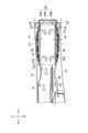
- FIG. 3 is a bottom view of the device body, showing an area where a cooling fan is arranged.
- 4 is a cross-sectional view of the electronic device taken along the line IV-IV shown in FIG. 3.
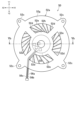
- FIG. FIG. 3 is a bottom view of the cooling fan.
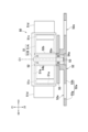
- 5A is a cross-sectional view of the cooling fan taken along the line Vb-Vb shown in FIG. 5A.
- X1 and X2 shown in FIG. 1 will be referred to as rightward and leftward, respectively, Y1 and Y2 will be referred to as forward and backward, respectively, and Z1 and Z2 will be referred to as upper and lower, respectively.
- X1 and X2 shown in FIG. 1 will be referred to as rightward and leftward, respectively
- Y1 and Y2 will be referred to as forward and backward, respectively
- Z1 and Z2 will be referred to as upper and lower, respectively.
- the electronic device 10 is, for example, an entertainment device that functions as a game device or an audio/visual device.
- the electronic device 10 outputs moving image data generated by executing a game program, video/audio data acquired through a network, and video/audio data acquired from a recording medium such as an optical disk to a display device such as a television.
- the electronic device may be a personal computer or a server computer.
- the electronic device 10 has a device main body 11 (see FIG. 2A).
- the device main body 11 has a housing 20.
- the housing 20 houses a circuit board 31.
- Various electronic components such as a CPU (Central Processing Unit) and a GPU (Graphical Processing Unit) are mounted on the circuit board 31.
- the housing 20 includes a heat radiator (such as a heat sink or a heat pipe) and a cooling fan 50 (not shown).
- the heat sink is connected to electronic components such as a CPU.
- the cooling fan 50 introduces outside air into the housing 20 and creates an airflow within the housing 20 that passes through the radiator.
- the housing 20 has flow paths therein in which air flows F1 and F2 are formed. (The white arrows in Figure 4 represent airflow.)
- the housing 20 may be composed of a plurality of members that are combined with each other.
- the housing 20 may include an upper housing 20A and a lower housing 20B that are combined with each other in the vertical direction.
- the housing 20 may include an exterior panel 20C (see FIG. 2A) that surrounds the front and side surfaces of the upper housing 20A and the lower housing 20B.
- the housing 20 includes an upper wall 21 (see FIG. 2A) that covers the upper side of the circuit board 31, the radiator, etc., and a lower wall 22 (see FIG. 2B) that covers the lower side of the circuit board 31, the radiator, etc. have.
- the device main body 11 includes an upper exterior panel 12 that covers the top surface 21a (outer surface of the top wall 21) of the device main body 11 and is attached to the top surface 21a.
- the upper exterior panel 12 may have a size that covers the entire upper surface 21a of the device main body 11, or may cover only a portion of the upper surface 21a (for example, an air intake port 21h described later). It may be the size.
- the device main body 11 includes a lower exterior panel 13 that covers a lower surface 22a (outer surface of the lower wall 22) of the device main body 11 and is attached to the lower surface 22a.
- the lower exterior panel 13 may have a size that covers the entire lower surface 22a of the device main body 11, or may cover only a portion of the lower surface 22a (for example, the air intake port 22h described later). It may be the size.
- the upper exterior panel 12 and the lower exterior panel 13 are removable from the device body 11.
- the upper exterior panel 12 has attachment portions 12a (see FIG. 2B) that are detachable from a plurality of attachment portions 21b (see FIG. 2A) formed on the upper surface 21a of the device main body 11.
- the lower exterior panel 13 has attachment portions 13a (see FIG. 2A) that are detachable from a plurality of attachment portions 22b (see FIG. 2B) formed on the lower surface 22a of the device main body 11.
- the upper wall 21 of the housing 20 is formed with an intake port 21h.
- the intake port 21h will be referred to as an upper housing intake port.
- an intake port 22h is formed in the lower wall 22 of the housing 20.
- the intake port 22h will be referred to as a lower housing intake port.
- the cooling fan 50 is arranged so that the axis C1 passing through the center of rotation thereof is directed in the vertical direction.
- the upper housing intake port 21h is formed above the cooling fan 50, and the lower housing intake port 22h is formed below the cooling fan 50.
- the intake port 21h is an opening in the upper wall 21 of the housing 20, and at least a portion of the intake port 21h is formed to overlap with the upper side of the cooling fan 50. May be exposed.
- the intake port 22h is an opening in the lower wall 22 of the housing 20, and at least a portion of the intake port 22h is formed so as to overlap the lower side of the cooling fan 50, so that the cooling fan is not connected to the cooling fan 50 from at least a portion of the intake port 22h. 50 exposures may be made.
- the electronic device 10 has an upper exterior panel 12, a lower exterior panel 13, and a housing 20 as its exterior members.
- the exterior member has intake ports Sa, Sb, Sc, and Sd for introducing external air into the electronic device 10.
- a gap G1 is formed between the upper housing intake port 21h and the upper exterior panel 12.
- This gap G1 functions as an air flow path from the intake ports Sa and Sb to the upper housing intake port 21h. (Hereinafter, this gap G1 will be referred to as an upper air intake path.)
- the air intake ports Sa and Sb are the ends of the upper air intake path G1 formed between the upper surface 21a of the housing 20 and the upper exterior panel 12. It is open toward the outside of the exterior member.
- a gap G2 is formed between the lower housing intake port 22h and the lower exterior panel 13.
- This gap G2 functions as an air flow path from the intake ports Sc and Sd to the lower housing intake port 22h.
- this gap G2 will be referred to as a lower intake passage.
- the intake ports Sc and Sd are the ends of the lower intake passage G2 formed between the lower surface 22a of the housing 20 and the lower exterior panel 13. It is open toward the outside of the exterior member.
- the upper intake passage G1 extends in a direction intersecting (substantially orthogonal to) the axis C1 of the cooling fan 50. That is, the upper air intake passage G1 extends in the radial direction of the cooling fan 50 along the upper wall 21 of the housing 20.
- the intake ports Sa and Sb between the upper exterior panel 12 and the upper wall 21 of the housing 20 are open in a direction intersecting the axis C1.
- the intake port Sa may open toward the front side of the electronic device 10
- the intake port Sb may open toward the right side of the electronic device 10.
- the intake port Sa and the intake port Sb are connected to each other, and may constitute one intake port spanning the corner of the electronic device 10.
- Louver members 24 may be attached to the intake ports Sa and Sb. The louver member 24 can suppress exposure of the upper intake passage G1 and the upper housing intake port 21h.
- the lower intake passage G2 extends in a direction intersecting (substantially orthogonal to) the axis C1 of the cooling fan 50. That is, the lower air intake passage G2 extends in the radial direction of the cooling fan 50 along the lower wall 22 of the housing 20.
- the intake ports Sc and Sd between the lower exterior panel 13 and the lower wall 22 of the housing 20 are open in a direction intersecting the axis C1.
- the intake port Sc may open toward the front side of the electronic device 10
- the intake port Sd may open toward the right side of the electronic device 10.
- the intake port Sc and the intake port Sd are connected to each other, and may constitute one intake port spanning the corner of the electronic device 10 .
- Louver members 25 may be attached to the intake ports Sc and Sd. The louver member 25 can suppress exposure of the lower intake passage G2 and the lower housing intake port 22h.
- the structure of the exterior member of the electronic device 10 is not limited to the examples shown in FIGS. 1 to 4.
- the opening directions of the intake ports Sa and Sb between the upper exterior panel 12 and the upper wall 21 of the housing 20 do not have to be two orthogonal directions.
- the intake port between the upper exterior panel 12 and the upper wall 21 of the housing 20 may be open only on the front side or only on the right side.
- the opening directions of the intake ports Sc and Sd between the lower exterior panel 13 and the lower wall 22 of the housing 20 do not have to be two orthogonal directions.
- the intake port between the lower exterior panel 13 and the lower wall 22 of the housing 20 may be open only on the front side or only on the right side.
- the exterior member may be formed into a box shape. In this case, the exterior member does not need to have the upper exterior panel 12 or the lower exterior panel 13.
- the upper housing intake port 21h may be covered by a protection plate 41 in which a plurality of openings are formed.
- the outer peripheral edge of the protection plate 41 may be attached to the edge of the upper housing intake port 21h.
- the protection plate 41 may be curved so that the center portion 41a thereof is higher than the outer peripheral edge of the protection plate 41. Thereby, air resistance caused by the protection plate 41 can be reduced.
- the lower housing intake port 22h may be covered by a protection plate 42 (see FIG. 2B) in which a plurality of openings are formed.
- the outer peripheral edge of the protection plate 42 may be attached to the edge of the lower housing intake port 22h.
- the protection plate 42 may be curved so that the center portion 42a thereof is lower than the outer peripheral edge of the protection plate 42. Thereby, air resistance caused by the protection plate 42 can be reduced.
- the cooling fan 50 includes a motor 51, a base member 52, a rotating shaft 53, a circuit board 55, and cables 56a, 56b, and 56c (see FIG. 5A). As described above, the cooling fan 50 is arranged so that the axis C1 along the center of rotation thereof is directed in the vertical direction of the electronic device 10.
- the motor 51 has a stator 51A that includes a coil, and a rotor 51B that is rotatable around the stator 51A.
- a plurality of fins 51d are formed on the outer peripheral surface of the rotor 51B.
- the rotor 51B has a cylindrical portion 51a that surrounds the outer periphery of the stator 51A, and an end wall portion 51b that is formed at an end of the cylindrical portion 51a and covers the stator 51A.
- a plurality of permanent magnets 51c are attached to the inner surface of the cylindrical portion 51a.
- the core of the stator 51A and the permanent magnet 51c face each other in the radial direction of the motor 51.
- the rotating shaft 53 is fixed to the end wall portion 51b of the rotor 51B, and is rotatable integrally with the rotor 51B.
- the base member 52 has a base plate portion 52a arranged in the direction of the axis C1 with respect to the motor 51. Moreover, the base member 52 has a support cylinder part 52b in which the rotating shaft 53 is arranged. This support cylinder part 52b supports the rotating shaft 53 via bearings 54a and 54b arranged inside the support cylinder part 52b. Further, a stator 51A is fixed to the outer circumferential surface of the support cylinder portion 52b.
- the base member 52 is formed by performing sheet metal processing on a metal plate.
- the base plate portion 52a has an annular outer ring portion 52g and an annular inner ring portion 52h.
- a plurality of attachment portions 52c (four attachment portions 52c in FIG. 5A) are formed on the outer peripheral edge of the outer ring portion 52g.
- the attachment portion 52c is attached to the edge of the lower housing intake port 22h described above using a fixing device such as a screw or bolt.
- the base member 52 has a plurality of bridges 52d extending from the inner edge of the outer ring portion 52g toward the inner ring portion 52h.
- the plurality of bridges 52d are formed at intervals in the rotation direction of the motor 51.
- An opening 52e is formed between two bridges 52d adjacent in the rotational direction.
- the circuit board 55 is arranged on the motor 51 side (upper side in the figure) with respect to the base plate portion 52a. That is, the circuit board 55 is disposed between the inner ring portion 52h of the base plate portion 52a and the stator 51A of the motor 51.
- the circuit board 55 has an opening 55n in its center.
- the support cylinder portion 52b of the base member 52 and the rotating shaft 53 are arranged inside the opening 55n.
- a circuit board 55 is attached to the base member 52.
- the circuit board 55 includes a switching element K2 that controls the current supplied to the motor 51, and a control IC (Integrated Circuit) (K1) that controls the switching element K2.
- the switching element K2 for example, a MOSFET (metal-oxide-semiconductor field-effect transistor) can be used.
- the switching element K2 may have a gate connected to the control IC (K1), a drain connected to the motor 51, and a source grounded.
- the control IC (K1) outputs an on/off signal for the switching element K2. That is, the control IC (K1) outputs a PWM signal to the switching element K2.
- the control IC (K1) drives the switching element K2 based on an instruction from the outside (for example, a processor mounted on the circuit board 31) or the output of a rotation sensor provided in the motor 51, and controls the motor. 51.
- a resistor (gate resistor) K2a may be placed between the control IC (K1) and the gate of the switching element K2, which is a MOSFET. The resistor K2a can stabilize the current supplied to the motor 51 by the action of the switching element K2.
- a protection element for stabilizing the control IC (K1) and/or the power supply voltage of the motor 51 may be mounted on the circuit board 55.
- a protection diode K3a may be mounted on the circuit board 55 as an example of a protection element.
- a protection diode K3a is placed between the power supply and ground and connected in series thereto. Further, the protection diode K3a is connected in parallel with, for example, the control IC (K1) and the motor 51, and prevents excessive voltage from being applied to them.
- a protection diode K3b may be mounted on the circuit board 55 as an example of a protection element.
- the protection diode K3b is arranged, for example, between the power supply and the switching element K2, and connected in series thereto. Note that, unlike the example shown in FIG. 7, only one of the two protection diodes K3a and K3b may be mounted on the circuit board 55. For example, only the protection diode K3a connected to ground may be mounted on the circuit board 55.
- a protection capacitor K4a may be mounted on the circuit board 55 as an example of a protection element.
- a protective capacitor K4a is placed between the power supply and ground and connected in series thereto.
- the protection capacitor K4a is connected in parallel to the control IC (K1) and the motor 51, for example, and keeps the voltage applied thereto constant.
- a protection capacitor K4b may be mounted on the circuit board 55 as an example of a protection element.
- a protective capacitor K4b is arranged between the power supply and the switching element K2 and connected in series thereto. Note that, unlike the example shown in FIG. 7, only one of the two protective capacitors K4a and K4b may be mounted on the circuit board 55. For example, only the protective capacitor K4a connected to ground may be mounted on the circuit board 55.
- a resistor for measuring the current supplied to the motor 51 that is, a shunt resistor K5 may be mounted on the circuit board 55.
- the shunt resistor K5 may be connected to the switching element K2 and ground.
- each component K may be mounted on either the upper surface (the surface on the motor 51 side) or the lower surface (the surface on the base plate portion 52a side) of the circuit board 55.
- the plurality of cables 56a, 56b, and 56c include cables for supplying drive current to the motor 51. Further, the plurality of cables 56a, 56b, and 56c include cables for supplying control signals related to driving the motor 51 from the outside (for example, a processor mounted on the circuit board 31) to the control IC (K1).
- the control signal is, for example, a signal instructing the rotation speed of the cooling fan 50.
- the number of cables 56a, 56b, and 56c shown in FIG. 5A is three, the number may be four (for example, two power cables and two signal cables).
- the component K mounted on the circuit board 55 is arranged so that it is difficult to be directly hit by the air flow F3.
- the arrangement of parts K will be explained in detail below.
- the intake ports Sc and Sd are separated from the axis C1 of the motor 51 in the radial direction of the motor 51. 3 and 6, a plane P1 is a plane passing through the axis C1 of the motor 51.
- a plane P1 is a plane passing through the axis C1 of the motor 51.
- At least one of the plurality of components (control IC (K1), switching element K2, protection diodes K3a and K3b, and protection capacitors K4a and K4b) mounted on the circuit board 55 is connected to the air intake port with the plane P1 in between. It is located on the opposite side from Sc and Sd. According to this arrangement of the parts (K1, K2, K2a, K3a, K3b, K4a, K4b), components in the air and dust adhering to the parts can be reduced.
- the plane P1 may be, for example, a plane that passes through the axis C1 of the motor 51 and is orthogonal to a straight line connecting the central portions M (see FIG. 3) of the intake ports Sc and Sd to the axis C1.
- the plane P1 may be a plane perpendicular to a straight line connecting the position where the width of the intake ports Sc and Sd is the largest and the axis C1.
- the width of the intake ports Sc and Sd is the width in the direction perpendicular to the opening direction of the intake ports Sc and Sd, and in the example shown in FIG. (This is the distance in the vertical direction from 12.)
- the plane P1 is a plane that is perpendicular to the straight line connecting the axis C1 and the position where the largest amount of air passes per unit time (the position where the speed of air flow is the fastest) in the intake ports Sc and Sd. It's okay.
- the main components among the eight components K described above may be located on the opposite side of the air intake ports Sc and Sd across the plane P1.
- the control IC (K1), the switching element K2, the grounded protection diode K3a and protection capacitor K4a, and the shunt resistor K5 may be located on the opposite side of the air intake ports Sc and Sd with the plane P1 in between. According to this, it is possible to effectively reduce the components and dust in the air that adhere to the parts, and also to reduce the influence of the components and the like on the drive of the motor 51.
- the protection diode K3b and the protection capacitor K4b may not be mounted on the circuit board 55.
- the protection diode K3b and the protection capacitor K4b may be placed on the same side of the plane P1 as the intake ports Sc and Sd.
- all of the plurality of components K mentioned above may be located on the opposite side of the air intake ports Sc and Sd across the plane P1. According to this, it is possible to more effectively reduce components in the air and dust adhering to the component K, and also to effectively reduce the influence of the components in the air and the like on the drive of the motor 51.
- control IC (K1), switching element K2, gate resistance K2a, protection diodes K3a and K3b, protection capacitors K4a and K4b, and shunt resistance K5) is sandwiched between plane P1. It may be located on the opposite side from the intake ports Sc and Sd.
- the control IC (K1) or the switching element K2, which is the most important element among the plurality of components K mentioned above, may be located on the opposite side of the air intake ports Sc and Sd with the plane P1 in between. According to this, the influence of adhesion of components in the air on the drive of the motor 51 can be reduced.
- the remaining parts may be located on the same side of the plane P1 as the air intake ports Sc and Sd, or the air intake ports Sc and Sd may be located on both sides of the plane P1. It may be located on the opposite side to Sd.
- the components disposed on the opposite side of the air intake ports Sc and Sd across the plane P1 may be larger in size than the other components. That is, the component having the largest size among the plurality of components K may be located on the opposite side of the air intake ports Sc and Sd across the plane P1. In this case, the remaining parts K may be located on the same side of the plane P1 as the intake ports Sc and Sd, or may be located on the opposite side of the plane P1 from the intake ports Sc and Sd.
- the components disposed on the opposite side of the air intake ports Sc and Sd across the plane P1 may be higher than other components.
- the tallest component among the plurality of components K may be located on the opposite side of the air intake ports Sc and Sd with the plane P1 in between.
- the remaining parts K may be located on the same side of the plane P1 as the intake ports Sc and Sd, or may be located on the opposite side of the plane P1 from the intake ports Sc and Sd.
- control IC (K1), switching element K2, gate resistance K2a, protection diodes K3a and K3b, protection capacitors K4a and K4b, and shunt resistance K5) are sandwiched between plane P1. It may be located on the opposite side from the intake ports Sc and Sd.
- control IC (K1) and the switching element K2, which are essential components for driving the motor 51 may be located on the opposite side of the air intake ports Sc and Sd with the plane P1 in between. According to this, the influence of adhesion of components in the air on the drive of the motor 51 can be effectively reduced.
- the remaining parts may be located on the side of the intake ports Sc and Sd with respect to the plane P1, or they may be located on the side of the intake ports Sc and Sd with respect to the plane P1. It may be located on the opposite side.
- control IC (K1), switching element K2, gate resistance K2a, protection diodes K3a and K3b, protection capacitors K4a and K4b, and shunt resistance K5) are connected to the plane P1. It may be located on the opposite side from the intake ports Sc and Sd.
- one of the gate resistance K2a, the protection diodes K3a and K3b, the capacitors K4a and K4b, and the shunt resistance K5 are connected to the air intake ports Sc and Sd with the plane P1 in between. It may be located on the opposite side.
- the remaining components may be located on the side of the intake ports Sc and Sd with respect to the plane P1, or may be located on the opposite side of the intake ports Sc and Sd with respect to the plane P1.
- the component K placed on the opposite side of the air intake ports Sc and Sd across the plane P1 may be a component that is not packaged with an insulating material such as resin.
- an insulating material such as resin
- the component K packaged with an insulating material such as resin may be located on the same side of the plane P1 as the intake ports Sc and Sd, or may be located on the same side of the plane P1 as the intake ports Sc and Sd. may be located on the opposite side. According to such a component arrangement, the influence of components in the air on unpackaged components can be reduced.
- the circuit board 55 has a connecting portion to which one end of the cables 56a, 56b, and 56c is connected.
- a connector may be provided at one end of the cables 56a, 56b, and 56c.
- the circuit board 55 may have a connector 55d as the above-mentioned connection portion, to which the connectors at the ends of the cables 56a, 56b, and 56c can be attached and detached.
- one end of the cables 56a, 56b, and 56c may be soldered to the circuit board 55. In this case, the soldered portion functions as the connection portion described above.
- the other ends of the cables 56a, 56b, and 56c are connected to, for example, another circuit board 31 housed in the housing 20.
- a housing groove 22d is formed in the lower wall 22 of the housing 20.
- the cables 56a, 56b, and 56c are laid in this housing groove 22d and extend to the inside of the housing 20.
- connection portion to which one end of the cables 56a, 56b, and 56c is connected may be located on the opposite side of the plane P1 from the intake ports Sc and Sd.
- the plane P1 is also a plane perpendicular to the straight line P2 connecting the axis C1 of the motor 51 and the connector 55d (connection portion).
- the connector 55d is located on the opposite side of the air intake ports Sc and Sd across the plane P1. This arrangement of the connector 55d facilitates electrical connection between the circuit board 55 and the device main body 11. Further, the cables 56a, 56b, and 56c can be easily installed without causing air resistance to the air flow formed between the lower exterior panel 13 and the lower wall 22 of the housing 20.
- the arrangement of the cooling fan 50 that reduces components and dust in the air that adheres to the parts can be 10, it is easy to realize.
- the cooling fan 50 is mounted on the electronic device 10 so that the connector 55d is located far from the air intake ports Sc and Sd as shown in FIGS. 3 and 6, the components in the air that adhere to these parts and Dust can be reduced.
- the position of the connector 55d is, for example, on the opposite side of the central portion M of the intake ports Sc and Sd across the axis C1.
- the connector 55d may intersect with a straight line connecting the axis C1 and the central portion M of the intake ports Sc and Sd.
- the position of the connector 55d may be on the opposite side of the axis C1 from the position where the width of the intake ports Sc and Sd is the largest.
- the connector 55d may intersect the straight line connecting the axis C1 and the position where the width of the intake ports Sc and Sd is the largest.
- the width of the intake ports Sc and Sd is the width in the direction perpendicular to the opening direction of the intake ports Sc and Sd.
- the upper surface 21a of the housing 20 and the upper exterior panel (This is the distance in the vertical direction from 12.)
- the position of the connector 55d is on the opposite side of the axis C1 from the position where the largest amount of air is introduced per unit time in the intake ports Sc and Sd (the position where the speed of air flow is the fastest). Good too. That is, the connector 55d may intersect with a straight line connecting the axis C1 and the position where the amount of air introduced per unit time is the largest in the intake ports Sc and Sd.
- the main components among the eight components K described above may be arranged on the same side as the connector 55d with respect to the plane P1.
- the control IC (K1), the switching element K2, the grounded protection diode K3a and protection capacitor K4a, and the shunt resistor K5 may be arranged on the same side of the plane P1 as the connector 55d.
- the protection diode K3b and the protection capacitor K4b may not be mounted on the circuit board 55.
- the protection diode K3b and the protection capacitor K4b may be arranged on the opposite side of the plane P1 from the connector 55d.
- all of the eight components described above may be arranged on the same side of the plane P1 as the connector 55d. According to this, when the cooling fan 50 is installed in the electronic device 10, it is possible to more effectively reduce components and dust in the air that adhere to these parts K, and also to reduce the influence of the adhesion on the drive of the motor 51. can be effectively reduced.
- control IC (K1), switching element K2, gate resistance K2a, protection diodes K3a and K3b, protection capacitors K4a and K4b, and shunt resistance K5) is placed on the plane P1.
- it may be placed on the same side as the connector 55d.
- the control IC (K1) or the switching element K2, which is the most important element among the plurality of components K described above, may be arranged on the same side of the plane P1 as the connector 55d. According to this, the influence of adhesion of components in the air on the drive of the motor 51 can be reduced.
- the remaining parts may be placed on the opposite side of the plane P1 from the connector 55d, or on the same side as the connector 55d with respect to the plane P1. It's okay.
- these components arranged on the same side as the connector 55d may be larger in size than the other components. That is, the component with the largest size among the plurality of components K may be located on the same side of the plane P1 as the connector 55d. In this case, the remaining components may be placed on the opposite side of the plane P1 from the connector 55d, or may be placed on the same side of the plane P1 as the connector 55d.
- a component disposed on the same side as the connector 55d with respect to the plane P1 may be a component higher than other components.
- the highest component among the plurality of components K may be located on the same side of the plane P1 as the connector 55d.
- the remaining parts K may be arranged on the opposite side of the plane P1 from the connector 55d, or may be arranged on the same side as the connector 55d with respect to the plane P1.
- control IC (K1), switching element K2, gate resistance K2a, protection diodes K3a, K3b, protection capacitors K4a, K4b, and shunt resistance K5) are placed on the plane P1.
- it may be placed on the same side as the connector 55d.
- the control IC (K1) and the switching element K2, which are essential components for driving the motor 51 may be arranged on the same side of the plane P1 as the connector 55d. According to this, the influence of adhesion of components in the air on the drive of the motor 51 can be effectively reduced.
- the remaining parts may be placed on the opposite side of the plane P1 from the connector 55d, or on the same side of the plane P1 as the connector 55d. may be placed.
- control IC (K1), switching element K2, gate resistance K2a/protection diode K3a, protection capacitor K4a, and shunt resistance K5) are connected to the connector with respect to the plane P1. It may be placed on the same side as 55d.
- one of the gate resistance K2a, the protection diode K3a, the protection capacitor Ka4, and the shunt resistance K5, the control IC (K1), and the switching element K2 are arranged on the same side of the plane P1 as the connector 55d. It's fine. According to this, the influence of adhesion of components in the air on the drive of the motor 51 can be further effectively reduced.
- the remaining components may be placed on the opposite side of the plane P1 from the connector 55d, or may be placed on the same side of the plane P1 as the connector 55d.
- the component placed on the same side of the plane P1 as the connector 55d may be a component that is not packaged with an insulating material such as resin.
- an insulating material such as resin
- the component packaged with an insulating material such as resin may be placed on the opposite side of the plane P1 from the connector 55d, or on the same side of the plane P1 as the connector 55d. Good too. According to such a component arrangement, the influence of components in the air on unpackaged components can be reduced.
- the cooling fan 50 and the exterior members (housing 20, upper exterior panel 12, and lower exterior panel 13) for accommodating the cooling fan 50 are prepared.
- a circuit board 31, a heat sink, etc. are also prepared to be placed inside the exterior member.
- the cooling fan 50 to be prepared includes fins 51d, a motor 51 for rotating the fins 51d, and a circuit board 55.
- the circuit board 55 is arranged in a direction along the axis C1 of the motor 51 with respect to the motor 51.
- a plurality of components K for driving the motor 51 are mounted on the circuit board 55.
- the exterior member has intake ports Sc and Sd for introducing air.
- the cooling fan 51 is arranged inside the exterior member so that the intake ports Sc and Sd are located apart from the motor 51 in the radial direction of the motor 51.
- a plurality of parts (the above-mentioned parts K1, K2, K3a, K3b, K4a, K4b, K5) are placed on the opposite side of the intake ports Sc and Sd across the plane P1 passing through the axis C1 of the motor 51.
- the cooling fan 50 is arranged inside the exterior member so that at least one of the cooling fans 50 is located inside the exterior member.
- all of the main components (components K1, K2, K3a, K4a, K5) mounted on the circuit board 55 are connected to the air intake port Sc across the plane P1 passing through the axis C1 of the motor 51.
- the cooling fan 50 may be arranged inside the exterior member so as to be located on the opposite side from Sd.
- a cooling fan is installed inside the exterior member so that two or three of the plurality of parts K are located on the opposite side of the air intake ports Sc and Sd across the plane P1. 50 may be arranged.
- a cooling fan 50 is installed inside the exterior member so that the largest component among the plurality of components K is located on the opposite side of the air intake ports Sc and Sd across the plane P1. may be placed.
- the electronic device 10 described above includes a cooling fan 50 and exterior members (housing 20, upper exterior panel 12, and lower exterior panel 13) having air intake ports Sc and Sd.
- the cooling fan 50 includes a fin 51d, a motor 51 for rotating the fin 51d, and a plurality of parts K for driving the motor 51, and is mounted with respect to the motor 51 in a direction along the axis C1 of the motor 51. It has a circuit board 55 arranged thereon.
- the plurality of components K include a switching element K2 that controls the current supplied to the motor 51, a control IC (K1) that controls the switching element K2, protection diodes K3a and K3b and protection capacitors K4a and K3b that stabilize the power supply voltage.
- the positions of the intake ports Sc and Sd are apart from the motor 51 in the radial direction of the motor 51.
- At least one of the plurality of parts (K1, K2, K3a, K3b, K4a, K4b, K5) is arranged on the opposite side of the intake ports Sc and Sd across a plane P1 passing through the axis C1 of the motor 51. There is. According to this component arrangement in the electronic device 10, components in the air and dust adhering to the component K can be reduced.
- two or three of the plurality of components K described above may be arranged on the opposite side of the air intake ports Sc and Sd across the plane P1 passing through the axis C1. good.
- the remaining components may be located on the same side of the plane P1 as the intake ports Sc and Sd.
- the cooling fan 50 described above is equipped with a motor 51 for rotating the fins 51d and a plurality of parts K for driving the motor 51, and is arranged in a direction along the axis C1 of the motor 51 with respect to the motor 51.
- the circuit board 55 includes a circuit board 55, cables 56a, 56b, and 56c, and a connector (connection portion) 55d provided on the circuit board 55 and to which the cables 56a, 56b, and 56c are connected.
- the plurality of components K include a switching element K2 that controls the current supplied to the motor 51, a control IC (K1) that controls the switching element K2, protection diodes K3a and K3b and protection capacitors K4a and K3b that stabilize the power supply voltage.
- At least one of the plurality of parts (K1, K2, K3a, K3b, K4a, K4b, K5) is on a plane P1 that is perpendicular to a straight line P2 that connects the axis C1 of the motor 51 and the connector 55d and that passes through the axis C1. In contrast, it is arranged on the same side as the connector 55d. Note that a plane perpendicular to the straight line P2 connecting the connector 55d and the axis C1 may be different from the plane P1.
- the above-mentioned one or more components that should be prevented from being directly hit by the air from the air intake ports Sc and Sd of the electronic device 10 are connected to the straight line P2. It may be located on the same side as the connector 55d with respect to a plane orthogonal to the plane.
- the arrangement of the cooling fan 50 that reduces components and dust in the air adhering to the component K can be adjusted to the electronic device 10. It is easy to realize this.
- two or three of the plurality of components (K1, K2, K3a, K3b, K4a, K4b, K5) described above are connected to the connector ( It may be arranged on the same side as the connection part) 55d.
- the remaining components may be located on the opposite side of the plane P1 from the connector 55d.
- the exterior member of the electronic device 10 has intake ports Sa and Sb (see FIG. 1) in its upper part, and intake ports Sc and Sd (see FIG. 1) in its lower part.
- the exterior member of the electronic device 10 has only the lower air intake ports Sc and Sd (see FIG. 1), that is, the air intake ports Sc and Sd on the side where the base member 52 is arranged, and the upper air intake ports Sa and Sd. It does not need to contain Sb.
- a control IC (K1), a switching element K2, a gate resistor K2a, protection diodes K3a and K3b, capacitors K4a and K4b, and a shunt resistor K5 are mounted on the circuit board 55.
- the cooling fan 50 may not include some of these parts K1, K2, K2a, K3a, K3b, K4a, K4b, and K5.
Landscapes
- Engineering & Computer Science (AREA)
- Microelectronics & Electronic Packaging (AREA)
- Physics & Mathematics (AREA)
- Thermal Sciences (AREA)
- Cooling Or The Like Of Electrical Apparatus (AREA)
Priority Applications (4)
| Application Number | Priority Date | Filing Date | Title |
|---|---|---|---|
| PCT/JP2022/017537 WO2023199388A1 (ja) | 2022-04-11 | 2022-04-11 | 冷却ファン、電子機器、及び電子機器の製造方法 |
| JP2024515199A JP7774133B2 (ja) | 2022-04-11 | 2022-04-11 | 冷却ファン、電子機器、及び電子機器の製造方法 |
| CN202280093456.XA CN118844124A (zh) | 2022-04-11 | 2022-04-11 | 冷却风扇、电子设备及电子设备的制造方法 |
| US18/855,385 US20250338431A1 (en) | 2022-04-11 | 2022-04-11 | Cooling fan, electronic device, and method for manufacturing electronic device |
Applications Claiming Priority (1)
| Application Number | Priority Date | Filing Date | Title |
|---|---|---|---|
| PCT/JP2022/017537 WO2023199388A1 (ja) | 2022-04-11 | 2022-04-11 | 冷却ファン、電子機器、及び電子機器の製造方法 |
Publications (1)
| Publication Number | Publication Date |
|---|---|
| WO2023199388A1 true WO2023199388A1 (ja) | 2023-10-19 |
Family
ID=88329235
Family Applications (1)
| Application Number | Title | Priority Date | Filing Date |
|---|---|---|---|
| PCT/JP2022/017537 Ceased WO2023199388A1 (ja) | 2022-04-11 | 2022-04-11 | 冷却ファン、電子機器、及び電子機器の製造方法 |
Country Status (4)
| Country | Link |
|---|---|
| US (1) | US20250338431A1 (https=) |
| JP (1) | JP7774133B2 (https=) |
| CN (1) | CN118844124A (https=) |
| WO (1) | WO2023199388A1 (https=) |
Cited By (1)
| Publication number | Priority date | Publication date | Assignee | Title |
|---|---|---|---|---|
| WO2026074900A1 (ja) * | 2024-10-01 | 2026-04-09 | 株式会社アイシン | 車載電子制御装置 |
Citations (6)
| Publication number | Priority date | Publication date | Assignee | Title |
|---|---|---|---|---|
| JPH05304379A (ja) * | 1992-04-28 | 1993-11-16 | Hitachi Ltd | 半導体冷却装置 |
| JP2000283089A (ja) * | 1999-03-31 | 2000-10-10 | Toshiba Home Technology Corp | ファンモータ |
| JP2008077436A (ja) * | 2006-09-21 | 2008-04-03 | Sony Computer Entertainment Inc | 電子機器 |
| WO2011138827A1 (ja) * | 2010-05-06 | 2011-11-10 | トヨタ自動車株式会社 | 電源制御システム |
| JP2013130094A (ja) * | 2011-12-21 | 2013-07-04 | Nippon Densan Corp | 遠心ファン |
| JP2018003686A (ja) * | 2016-06-30 | 2018-01-11 | ミネベアミツミ株式会社 | 遠心ファン |
-
2022
- 2022-04-11 WO PCT/JP2022/017537 patent/WO2023199388A1/ja not_active Ceased
- 2022-04-11 US US18/855,385 patent/US20250338431A1/en active Pending
- 2022-04-11 JP JP2024515199A patent/JP7774133B2/ja active Active
- 2022-04-11 CN CN202280093456.XA patent/CN118844124A/zh active Pending
Patent Citations (6)
| Publication number | Priority date | Publication date | Assignee | Title |
|---|---|---|---|---|
| JPH05304379A (ja) * | 1992-04-28 | 1993-11-16 | Hitachi Ltd | 半導体冷却装置 |
| JP2000283089A (ja) * | 1999-03-31 | 2000-10-10 | Toshiba Home Technology Corp | ファンモータ |
| JP2008077436A (ja) * | 2006-09-21 | 2008-04-03 | Sony Computer Entertainment Inc | 電子機器 |
| WO2011138827A1 (ja) * | 2010-05-06 | 2011-11-10 | トヨタ自動車株式会社 | 電源制御システム |
| JP2013130094A (ja) * | 2011-12-21 | 2013-07-04 | Nippon Densan Corp | 遠心ファン |
| JP2018003686A (ja) * | 2016-06-30 | 2018-01-11 | ミネベアミツミ株式会社 | 遠心ファン |
Cited By (1)
| Publication number | Priority date | Publication date | Assignee | Title |
|---|---|---|---|---|
| WO2026074900A1 (ja) * | 2024-10-01 | 2026-04-09 | 株式会社アイシン | 車載電子制御装置 |
Also Published As
| Publication number | Publication date |
|---|---|
| JP7774133B2 (ja) | 2025-11-20 |
| JPWO2023199388A1 (https=) | 2023-10-19 |
| CN118844124A (zh) | 2024-10-25 |
| US20250338431A1 (en) | 2025-10-30 |
Similar Documents
| Publication | Publication Date | Title |
|---|---|---|
| US6830440B1 (en) | External rotor brushless DC motor | |
| US6841957B2 (en) | Low profile motor | |
| US8157540B2 (en) | Fan assembly | |
| US7903406B2 (en) | Centrifugal fan | |
| EP0874442A2 (en) | An electric motor having an improved airflow cooling system | |
| JP6863662B2 (ja) | 空撮カメラ及び電子機器並びにそれを備えた無人飛行体 | |
| JPH10224061A (ja) | ヒートシンクユニット及び電子機器 | |
| WO2023199388A1 (ja) | 冷却ファン、電子機器、及び電子機器の製造方法 | |
| CN114902823B (zh) | 冷却构造体和电气装置 | |
| JP2020111326A (ja) | 空撮カメラ及び電子機器並びにそれを備えた無人飛行体 | |
| JP3710089B2 (ja) | 遊技機の制御装置 | |
| CN1276697C (zh) | 空气导管和采用这种空气导管的电子设备 | |
| JP2004049292A (ja) | 遊技機の制御装置 | |
| JP7797693B2 (ja) | 冷却ファン及び電子機器 | |
| JPWO2024101228A5 (https=) | ||
| JP2000124648A (ja) | ヒートシンクファン装置 | |
| JP2005192827A (ja) | 遊技機 | |
| JP5516629B2 (ja) | ファン装置 | |
| JP5892122B2 (ja) | ファン装置及び電子機器 | |
| JP3711539B2 (ja) | 遊技機の制御装置 | |
| JP7273149B2 (ja) | 電子機器 | |
| JP4916148B2 (ja) | 遊技電気部品冷却装置 | |
| JP3254961B2 (ja) | 空気調和機の室内ユニット | |
| WO2026069917A1 (ja) | インバータ装置および回転機械 | |
| JP2004049288A (ja) | 遊技機の制御装置 |
Legal Events
| Date | Code | Title | Description |
|---|---|---|---|
| 121 | Ep: the epo has been informed by wipo that ep was designated in this application |
Ref document number: 22937368 Country of ref document: EP Kind code of ref document: A1 |
|
| WWE | Wipo information: entry into national phase |
Ref document number: 202280093456.X Country of ref document: CN |
|
| WWE | Wipo information: entry into national phase |
Ref document number: 18855385 Country of ref document: US |
|
| WWE | Wipo information: entry into national phase |
Ref document number: 2024515199 Country of ref document: JP |
|
| REG | Reference to national code |
Ref country code: BR Ref legal event code: B01A Ref document number: 112024020786 Country of ref document: BR |
|
| NENP | Non-entry into the national phase |
Ref country code: DE |
|
| ENP | Entry into the national phase |
Ref document number: 112024020786 Country of ref document: BR Kind code of ref document: A2 Effective date: 20241007 |
|
| 122 | Ep: pct application non-entry in european phase |
Ref document number: 22937368 Country of ref document: EP Kind code of ref document: A1 |
|
| WWP | Wipo information: published in national office |
Ref document number: 18855385 Country of ref document: US |