WO2023199388A1 - Cooling fan, electronic device, and method for producing electronic device - Google Patents
Cooling fan, electronic device, and method for producing electronic device Download PDFInfo
- Publication number
- WO2023199388A1 WO2023199388A1 PCT/JP2022/017537 JP2022017537W WO2023199388A1 WO 2023199388 A1 WO2023199388 A1 WO 2023199388A1 JP 2022017537 W JP2022017537 W JP 2022017537W WO 2023199388 A1 WO2023199388 A1 WO 2023199388A1
- Authority
- WO
- WIPO (PCT)
- Prior art keywords
- motor
- switching element
- cooling fan
- plane
- components
- Prior art date
Links
- 238000001816 cooling Methods 0.000 title claims abstract description 85
- 238000004519 manufacturing process Methods 0.000 title claims description 6
- 238000000034 method Methods 0.000 claims description 9
- 239000003990 capacitor Substances 0.000 abstract description 32
- 239000000428 dust Substances 0.000 abstract description 19
- 230000001681 protective effect Effects 0.000 abstract description 8
- 239000000126 substance Substances 0.000 abstract 1
- 230000002093 peripheral effect Effects 0.000 description 6
- 239000011810 insulating material Substances 0.000 description 4
- 239000011347 resin Substances 0.000 description 4
- 229920005989 resin Polymers 0.000 description 4
- 239000004615 ingredient Substances 0.000 description 2
- 239000002184 metal Substances 0.000 description 2
- 230000000087 stabilizing effect Effects 0.000 description 2
- 230000004308 accommodation Effects 0.000 description 1
- 238000010586 diagram Methods 0.000 description 1
- 230000005669 field effect Effects 0.000 description 1
- 230000003287 optical effect Effects 0.000 description 1
- 239000004065 semiconductor Substances 0.000 description 1
- 230000000007 visual effect Effects 0.000 description 1
Images


Classifications
-
- H—ELECTRICITY
- H05—ELECTRIC TECHNIQUES NOT OTHERWISE PROVIDED FOR
- H05K—PRINTED CIRCUITS; CASINGS OR CONSTRUCTIONAL DETAILS OF ELECTRIC APPARATUS; MANUFACTURE OF ASSEMBLAGES OF ELECTRICAL COMPONENTS
- H05K7/00—Constructional details common to different types of electric apparatus
- H05K7/20—Modifications to facilitate cooling, ventilating, or heating
Definitions
- the present disclosure relates to a cooling fan, an electronic device, and a method of manufacturing the electronic device.
- Cooling fans are placed inside electronic devices such as game devices, personal computers, and server computers to cool heat-generating components such as CPUs and GPUs mounted on circuit boards.
- An air intake port for introducing external air is formed in an exterior member of an electronic device.
- Patent Document 1 listed below discloses an example of such an electronic device.
- a cooling fan has a circuit board on which various electronic components are mounted, such as a switching element (FET) that controls the current supplied to the motor, and a control IC that controls the switching element according to signals input from the outside. ing.
- FET switching element
- control IC controls the switching element according to signals input from the outside.
- the electronic device proposed in the present disclosure includes a cooling fan, and an exterior member in which the cooling fan is disposed and has an air intake port.
- the cooling fan includes fins, a motor for rotating the fins, and a plurality of parts for driving the motor, and is arranged in a direction along the axis of the motor with respect to the motor. It has a circuit board.
- the plurality of components include a switching element that controls the current supplied to the motor, a control IC that controls the switching element, a protection element that stabilizes the power supply voltage, and a protection element that measures the current supplied to the motor. including at least one resistor for.
- the position of the air intake port is spaced apart from the motor in a radial direction of the motor.
- the at least one of the plurality of components is disposed on the opposite side of the intake port across a plane passing through the axis of the motor. According to this electronic device, components in the air and dust that adhere to electronic components on the circuit board of the cooling fan can be reduced.
- An electronic device proposed in the present disclosure includes a fin, a motor for rotating the fin, and a plurality of components for driving the motor, and is mounted with respect to the motor in a direction along the axis of the motor.
- the device includes a circuit board arranged thereon, at least one cable, and a connection part provided on the circuit board and connected to the at least one cable.
- the plurality of components include a switching element that controls the current supplied to the motor, a control IC that controls the switching element, a protection element that stabilizes the power supply voltage, and a protection element that measures the current supplied to the motor. including at least one resistor for.
- the at least one of the plurality of parts is perpendicular to a straight line connecting the axis of the motor and the connection part and disposed on the same side as the connection part with respect to a plane passing through the axis. has been done.
- this cooling fan when the cooling fan is mounted on an electronic device, it is easy to realize an arrangement that reduces components in the air and dust that adhere to electronic components on the circuit board of the cooling fan.
- a method for manufacturing an electronic device proposed in the present disclosure includes a fin, a motor for rotating the fin, and a plurality of components for driving the motor, and a fin, a motor for rotating the fin, and a plurality of components for driving the motor.
- a step of preparing a cooling fan having a circuit board disposed in a direction a step of preparing an exterior member having an intake port for introducing air and accommodating the cooling fan;
- the method includes an assembling step of arranging the cooling fan inside the exterior member so that the intake port is located away from the motor in a radial direction of the motor.
- the plurality of components include a switching element for controlling the current supplied to the motor, a control IC for controlling the switching element, a protection element for stabilizing the power supply voltage, and a measuring element for measuring the current supplied to the motor. at least one of the resistors.
- the cooling fan is installed inside the exterior member so that the at least one of the plurality of parts is located on the opposite side of the intake port across a plane passing through the axis of the motor. Deploy. According to this manufacturing method, components in the air and dust that adhere to electronic components on the circuit board of the cooling fan can be reduced.
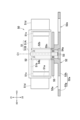
- FIG. 1 is a perspective view showing an example of an electronic device proposed in the present disclosure.
- FIG. 2 is an exploded perspective view of the main body, upper exterior panel, and lower exterior panel of the electronic device shown in FIG. 1, viewed diagonally from above.
- FIG. 2 is an exploded perspective view of the main body, upper exterior panel, and lower exterior panel of the electronic device shown in FIG. 1, viewed diagonally from below.
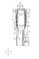
- FIG. 3 is a bottom view of the device body, showing an area where a cooling fan is arranged.
- 4 is a cross-sectional view of the electronic device taken along the line IV-IV shown in FIG. 3.
- FIG. FIG. 3 is a bottom view of the cooling fan.
- 5A is a cross-sectional view of the cooling fan taken along the line Vb-Vb shown in FIG. 5A.
- X1 and X2 shown in FIG. 1 will be referred to as rightward and leftward, respectively, Y1 and Y2 will be referred to as forward and backward, respectively, and Z1 and Z2 will be referred to as upper and lower, respectively.
- X1 and X2 shown in FIG. 1 will be referred to as rightward and leftward, respectively
- Y1 and Y2 will be referred to as forward and backward, respectively
- Z1 and Z2 will be referred to as upper and lower, respectively.
- the electronic device 10 is, for example, an entertainment device that functions as a game device or an audio/visual device.
- the electronic device 10 outputs moving image data generated by executing a game program, video/audio data acquired through a network, and video/audio data acquired from a recording medium such as an optical disk to a display device such as a television.
- the electronic device may be a personal computer or a server computer.
- the electronic device 10 has a device main body 11 (see FIG. 2A).
- the device main body 11 has a housing 20.
- the housing 20 houses a circuit board 31.
- Various electronic components such as a CPU (Central Processing Unit) and a GPU (Graphical Processing Unit) are mounted on the circuit board 31.
- the housing 20 includes a heat radiator (such as a heat sink or a heat pipe) and a cooling fan 50 (not shown).
- the heat sink is connected to electronic components such as a CPU.
- the cooling fan 50 introduces outside air into the housing 20 and creates an airflow within the housing 20 that passes through the radiator.
- the housing 20 has flow paths therein in which air flows F1 and F2 are formed. (The white arrows in Figure 4 represent airflow.)
- the housing 20 may be composed of a plurality of members that are combined with each other.
- the housing 20 may include an upper housing 20A and a lower housing 20B that are combined with each other in the vertical direction.
- the housing 20 may include an exterior panel 20C (see FIG. 2A) that surrounds the front and side surfaces of the upper housing 20A and the lower housing 20B.
- the housing 20 includes an upper wall 21 (see FIG. 2A) that covers the upper side of the circuit board 31, the radiator, etc., and a lower wall 22 (see FIG. 2B) that covers the lower side of the circuit board 31, the radiator, etc. have.
- the device main body 11 includes an upper exterior panel 12 that covers the top surface 21a (outer surface of the top wall 21) of the device main body 11 and is attached to the top surface 21a.
- the upper exterior panel 12 may have a size that covers the entire upper surface 21a of the device main body 11, or may cover only a portion of the upper surface 21a (for example, an air intake port 21h described later). It may be the size.
- the device main body 11 includes a lower exterior panel 13 that covers a lower surface 22a (outer surface of the lower wall 22) of the device main body 11 and is attached to the lower surface 22a.
- the lower exterior panel 13 may have a size that covers the entire lower surface 22a of the device main body 11, or may cover only a portion of the lower surface 22a (for example, the air intake port 22h described later). It may be the size.
- the upper exterior panel 12 and the lower exterior panel 13 are removable from the device body 11.
- the upper exterior panel 12 has attachment portions 12a (see FIG. 2B) that are detachable from a plurality of attachment portions 21b (see FIG. 2A) formed on the upper surface 21a of the device main body 11.
- the lower exterior panel 13 has attachment portions 13a (see FIG. 2A) that are detachable from a plurality of attachment portions 22b (see FIG. 2B) formed on the lower surface 22a of the device main body 11.
- the upper wall 21 of the housing 20 is formed with an intake port 21h.
- the intake port 21h will be referred to as an upper housing intake port.
- an intake port 22h is formed in the lower wall 22 of the housing 20.
- the intake port 22h will be referred to as a lower housing intake port.
- the cooling fan 50 is arranged so that the axis C1 passing through the center of rotation thereof is directed in the vertical direction.
- the upper housing intake port 21h is formed above the cooling fan 50, and the lower housing intake port 22h is formed below the cooling fan 50.
- the intake port 21h is an opening in the upper wall 21 of the housing 20, and at least a portion of the intake port 21h is formed to overlap with the upper side of the cooling fan 50. May be exposed.
- the intake port 22h is an opening in the lower wall 22 of the housing 20, and at least a portion of the intake port 22h is formed so as to overlap the lower side of the cooling fan 50, so that the cooling fan is not connected to the cooling fan 50 from at least a portion of the intake port 22h. 50 exposures may be made.
- the electronic device 10 has an upper exterior panel 12, a lower exterior panel 13, and a housing 20 as its exterior members.
- the exterior member has intake ports Sa, Sb, Sc, and Sd for introducing external air into the electronic device 10.
- a gap G1 is formed between the upper housing intake port 21h and the upper exterior panel 12.
- This gap G1 functions as an air flow path from the intake ports Sa and Sb to the upper housing intake port 21h. (Hereinafter, this gap G1 will be referred to as an upper air intake path.)
- the air intake ports Sa and Sb are the ends of the upper air intake path G1 formed between the upper surface 21a of the housing 20 and the upper exterior panel 12. It is open toward the outside of the exterior member.
- a gap G2 is formed between the lower housing intake port 22h and the lower exterior panel 13.
- This gap G2 functions as an air flow path from the intake ports Sc and Sd to the lower housing intake port 22h.
- this gap G2 will be referred to as a lower intake passage.
- the intake ports Sc and Sd are the ends of the lower intake passage G2 formed between the lower surface 22a of the housing 20 and the lower exterior panel 13. It is open toward the outside of the exterior member.
- the upper intake passage G1 extends in a direction intersecting (substantially orthogonal to) the axis C1 of the cooling fan 50. That is, the upper air intake passage G1 extends in the radial direction of the cooling fan 50 along the upper wall 21 of the housing 20.
- the intake ports Sa and Sb between the upper exterior panel 12 and the upper wall 21 of the housing 20 are open in a direction intersecting the axis C1.
- the intake port Sa may open toward the front side of the electronic device 10
- the intake port Sb may open toward the right side of the electronic device 10.
- the intake port Sa and the intake port Sb are connected to each other, and may constitute one intake port spanning the corner of the electronic device 10.
- Louver members 24 may be attached to the intake ports Sa and Sb. The louver member 24 can suppress exposure of the upper intake passage G1 and the upper housing intake port 21h.
- the lower intake passage G2 extends in a direction intersecting (substantially orthogonal to) the axis C1 of the cooling fan 50. That is, the lower air intake passage G2 extends in the radial direction of the cooling fan 50 along the lower wall 22 of the housing 20.
- the intake ports Sc and Sd between the lower exterior panel 13 and the lower wall 22 of the housing 20 are open in a direction intersecting the axis C1.
- the intake port Sc may open toward the front side of the electronic device 10
- the intake port Sd may open toward the right side of the electronic device 10.
- the intake port Sc and the intake port Sd are connected to each other, and may constitute one intake port spanning the corner of the electronic device 10 .
- Louver members 25 may be attached to the intake ports Sc and Sd. The louver member 25 can suppress exposure of the lower intake passage G2 and the lower housing intake port 22h.
- the structure of the exterior member of the electronic device 10 is not limited to the examples shown in FIGS. 1 to 4.
- the opening directions of the intake ports Sa and Sb between the upper exterior panel 12 and the upper wall 21 of the housing 20 do not have to be two orthogonal directions.
- the intake port between the upper exterior panel 12 and the upper wall 21 of the housing 20 may be open only on the front side or only on the right side.
- the opening directions of the intake ports Sc and Sd between the lower exterior panel 13 and the lower wall 22 of the housing 20 do not have to be two orthogonal directions.
- the intake port between the lower exterior panel 13 and the lower wall 22 of the housing 20 may be open only on the front side or only on the right side.
- the exterior member may be formed into a box shape. In this case, the exterior member does not need to have the upper exterior panel 12 or the lower exterior panel 13.
- the upper housing intake port 21h may be covered by a protection plate 41 in which a plurality of openings are formed.
- the outer peripheral edge of the protection plate 41 may be attached to the edge of the upper housing intake port 21h.
- the protection plate 41 may be curved so that the center portion 41a thereof is higher than the outer peripheral edge of the protection plate 41. Thereby, air resistance caused by the protection plate 41 can be reduced.
- the lower housing intake port 22h may be covered by a protection plate 42 (see FIG. 2B) in which a plurality of openings are formed.
- the outer peripheral edge of the protection plate 42 may be attached to the edge of the lower housing intake port 22h.
- the protection plate 42 may be curved so that the center portion 42a thereof is lower than the outer peripheral edge of the protection plate 42. Thereby, air resistance caused by the protection plate 42 can be reduced.
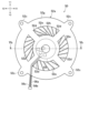
- the cooling fan 50 includes a motor 51, a base member 52, a rotating shaft 53, a circuit board 55, and cables 56a, 56b, and 56c (see FIG. 5A). As described above, the cooling fan 50 is arranged so that the axis C1 along the center of rotation thereof is directed in the vertical direction of the electronic device 10.
- the motor 51 has a stator 51A that includes a coil, and a rotor 51B that is rotatable around the stator 51A.
- a plurality of fins 51d are formed on the outer peripheral surface of the rotor 51B.
- the rotor 51B has a cylindrical portion 51a that surrounds the outer periphery of the stator 51A, and an end wall portion 51b that is formed at an end of the cylindrical portion 51a and covers the stator 51A.
- a plurality of permanent magnets 51c are attached to the inner surface of the cylindrical portion 51a.
- the core of the stator 51A and the permanent magnet 51c face each other in the radial direction of the motor 51.
- the rotating shaft 53 is fixed to the end wall portion 51b of the rotor 51B, and is rotatable integrally with the rotor 51B.
- the base member 52 has a base plate portion 52a arranged in the direction of the axis C1 with respect to the motor 51. Moreover, the base member 52 has a support cylinder part 52b in which the rotating shaft 53 is arranged. This support cylinder part 52b supports the rotating shaft 53 via bearings 54a and 54b arranged inside the support cylinder part 52b. Further, a stator 51A is fixed to the outer circumferential surface of the support cylinder portion 52b.
- the base member 52 is formed by performing sheet metal processing on a metal plate.
- the base plate portion 52a has an annular outer ring portion 52g and an annular inner ring portion 52h.
- a plurality of attachment portions 52c (four attachment portions 52c in FIG. 5A) are formed on the outer peripheral edge of the outer ring portion 52g.
- the attachment portion 52c is attached to the edge of the lower housing intake port 22h described above using a fixing device such as a screw or bolt.
- the base member 52 has a plurality of bridges 52d extending from the inner edge of the outer ring portion 52g toward the inner ring portion 52h.
- the plurality of bridges 52d are formed at intervals in the rotation direction of the motor 51.
- An opening 52e is formed between two bridges 52d adjacent in the rotational direction.
- the circuit board 55 is arranged on the motor 51 side (upper side in the figure) with respect to the base plate portion 52a. That is, the circuit board 55 is disposed between the inner ring portion 52h of the base plate portion 52a and the stator 51A of the motor 51.
- the circuit board 55 has an opening 55n in its center.
- the support cylinder portion 52b of the base member 52 and the rotating shaft 53 are arranged inside the opening 55n.
- a circuit board 55 is attached to the base member 52.
- the circuit board 55 includes a switching element K2 that controls the current supplied to the motor 51, and a control IC (Integrated Circuit) (K1) that controls the switching element K2.
- the switching element K2 for example, a MOSFET (metal-oxide-semiconductor field-effect transistor) can be used.
- the switching element K2 may have a gate connected to the control IC (K1), a drain connected to the motor 51, and a source grounded.
- the control IC (K1) outputs an on/off signal for the switching element K2. That is, the control IC (K1) outputs a PWM signal to the switching element K2.
- the control IC (K1) drives the switching element K2 based on an instruction from the outside (for example, a processor mounted on the circuit board 31) or the output of a rotation sensor provided in the motor 51, and controls the motor. 51.
- a resistor (gate resistor) K2a may be placed between the control IC (K1) and the gate of the switching element K2, which is a MOSFET. The resistor K2a can stabilize the current supplied to the motor 51 by the action of the switching element K2.
- a protection element for stabilizing the control IC (K1) and/or the power supply voltage of the motor 51 may be mounted on the circuit board 55.
- a protection diode K3a may be mounted on the circuit board 55 as an example of a protection element.
- a protection diode K3a is placed between the power supply and ground and connected in series thereto. Further, the protection diode K3a is connected in parallel with, for example, the control IC (K1) and the motor 51, and prevents excessive voltage from being applied to them.
- a protection diode K3b may be mounted on the circuit board 55 as an example of a protection element.
- the protection diode K3b is arranged, for example, between the power supply and the switching element K2, and connected in series thereto. Note that, unlike the example shown in FIG. 7, only one of the two protection diodes K3a and K3b may be mounted on the circuit board 55. For example, only the protection diode K3a connected to ground may be mounted on the circuit board 55.
- a protection capacitor K4a may be mounted on the circuit board 55 as an example of a protection element.
- a protective capacitor K4a is placed between the power supply and ground and connected in series thereto.
- the protection capacitor K4a is connected in parallel to the control IC (K1) and the motor 51, for example, and keeps the voltage applied thereto constant.
- a protection capacitor K4b may be mounted on the circuit board 55 as an example of a protection element.
- a protective capacitor K4b is arranged between the power supply and the switching element K2 and connected in series thereto. Note that, unlike the example shown in FIG. 7, only one of the two protective capacitors K4a and K4b may be mounted on the circuit board 55. For example, only the protective capacitor K4a connected to ground may be mounted on the circuit board 55.
- a resistor for measuring the current supplied to the motor 51 that is, a shunt resistor K5 may be mounted on the circuit board 55.
- the shunt resistor K5 may be connected to the switching element K2 and ground.
- each component K may be mounted on either the upper surface (the surface on the motor 51 side) or the lower surface (the surface on the base plate portion 52a side) of the circuit board 55.
- the plurality of cables 56a, 56b, and 56c include cables for supplying drive current to the motor 51. Further, the plurality of cables 56a, 56b, and 56c include cables for supplying control signals related to driving the motor 51 from the outside (for example, a processor mounted on the circuit board 31) to the control IC (K1).
- the control signal is, for example, a signal instructing the rotation speed of the cooling fan 50.
- the number of cables 56a, 56b, and 56c shown in FIG. 5A is three, the number may be four (for example, two power cables and two signal cables).
- the component K mounted on the circuit board 55 is arranged so that it is difficult to be directly hit by the air flow F3.
- the arrangement of parts K will be explained in detail below.
- the intake ports Sc and Sd are separated from the axis C1 of the motor 51 in the radial direction of the motor 51. 3 and 6, a plane P1 is a plane passing through the axis C1 of the motor 51.
- a plane P1 is a plane passing through the axis C1 of the motor 51.
- At least one of the plurality of components (control IC (K1), switching element K2, protection diodes K3a and K3b, and protection capacitors K4a and K4b) mounted on the circuit board 55 is connected to the air intake port with the plane P1 in between. It is located on the opposite side from Sc and Sd. According to this arrangement of the parts (K1, K2, K2a, K3a, K3b, K4a, K4b), components in the air and dust adhering to the parts can be reduced.
- the plane P1 may be, for example, a plane that passes through the axis C1 of the motor 51 and is orthogonal to a straight line connecting the central portions M (see FIG. 3) of the intake ports Sc and Sd to the axis C1.
- the plane P1 may be a plane perpendicular to a straight line connecting the position where the width of the intake ports Sc and Sd is the largest and the axis C1.
- the width of the intake ports Sc and Sd is the width in the direction perpendicular to the opening direction of the intake ports Sc and Sd, and in the example shown in FIG. (This is the distance in the vertical direction from 12.)
- the plane P1 is a plane that is perpendicular to the straight line connecting the axis C1 and the position where the largest amount of air passes per unit time (the position where the speed of air flow is the fastest) in the intake ports Sc and Sd. It's okay.
- the main components among the eight components K described above may be located on the opposite side of the air intake ports Sc and Sd across the plane P1.
- the control IC (K1), the switching element K2, the grounded protection diode K3a and protection capacitor K4a, and the shunt resistor K5 may be located on the opposite side of the air intake ports Sc and Sd with the plane P1 in between. According to this, it is possible to effectively reduce the components and dust in the air that adhere to the parts, and also to reduce the influence of the components and the like on the drive of the motor 51.
- the protection diode K3b and the protection capacitor K4b may not be mounted on the circuit board 55.
- the protection diode K3b and the protection capacitor K4b may be placed on the same side of the plane P1 as the intake ports Sc and Sd.
- all of the plurality of components K mentioned above may be located on the opposite side of the air intake ports Sc and Sd across the plane P1. According to this, it is possible to more effectively reduce components in the air and dust adhering to the component K, and also to effectively reduce the influence of the components in the air and the like on the drive of the motor 51.
- control IC (K1), switching element K2, gate resistance K2a, protection diodes K3a and K3b, protection capacitors K4a and K4b, and shunt resistance K5) is sandwiched between plane P1. It may be located on the opposite side from the intake ports Sc and Sd.
- the control IC (K1) or the switching element K2, which is the most important element among the plurality of components K mentioned above, may be located on the opposite side of the air intake ports Sc and Sd with the plane P1 in between. According to this, the influence of adhesion of components in the air on the drive of the motor 51 can be reduced.
- the remaining parts may be located on the same side of the plane P1 as the air intake ports Sc and Sd, or the air intake ports Sc and Sd may be located on both sides of the plane P1. It may be located on the opposite side to Sd.
- the components disposed on the opposite side of the air intake ports Sc and Sd across the plane P1 may be larger in size than the other components. That is, the component having the largest size among the plurality of components K may be located on the opposite side of the air intake ports Sc and Sd across the plane P1. In this case, the remaining parts K may be located on the same side of the plane P1 as the intake ports Sc and Sd, or may be located on the opposite side of the plane P1 from the intake ports Sc and Sd.
- the components disposed on the opposite side of the air intake ports Sc and Sd across the plane P1 may be higher than other components.
- the tallest component among the plurality of components K may be located on the opposite side of the air intake ports Sc and Sd with the plane P1 in between.
- the remaining parts K may be located on the same side of the plane P1 as the intake ports Sc and Sd, or may be located on the opposite side of the plane P1 from the intake ports Sc and Sd.
- control IC (K1), switching element K2, gate resistance K2a, protection diodes K3a and K3b, protection capacitors K4a and K4b, and shunt resistance K5) are sandwiched between plane P1. It may be located on the opposite side from the intake ports Sc and Sd.
- control IC (K1) and the switching element K2, which are essential components for driving the motor 51 may be located on the opposite side of the air intake ports Sc and Sd with the plane P1 in between. According to this, the influence of adhesion of components in the air on the drive of the motor 51 can be effectively reduced.
- the remaining parts may be located on the side of the intake ports Sc and Sd with respect to the plane P1, or they may be located on the side of the intake ports Sc and Sd with respect to the plane P1. It may be located on the opposite side.
- control IC (K1), switching element K2, gate resistance K2a, protection diodes K3a and K3b, protection capacitors K4a and K4b, and shunt resistance K5) are connected to the plane P1. It may be located on the opposite side from the intake ports Sc and Sd.
- one of the gate resistance K2a, the protection diodes K3a and K3b, the capacitors K4a and K4b, and the shunt resistance K5 are connected to the air intake ports Sc and Sd with the plane P1 in between. It may be located on the opposite side.
- the remaining components may be located on the side of the intake ports Sc and Sd with respect to the plane P1, or may be located on the opposite side of the intake ports Sc and Sd with respect to the plane P1.
- the component K placed on the opposite side of the air intake ports Sc and Sd across the plane P1 may be a component that is not packaged with an insulating material such as resin.
- an insulating material such as resin
- the component K packaged with an insulating material such as resin may be located on the same side of the plane P1 as the intake ports Sc and Sd, or may be located on the same side of the plane P1 as the intake ports Sc and Sd. may be located on the opposite side. According to such a component arrangement, the influence of components in the air on unpackaged components can be reduced.
- the circuit board 55 has a connecting portion to which one end of the cables 56a, 56b, and 56c is connected.
- a connector may be provided at one end of the cables 56a, 56b, and 56c.
- the circuit board 55 may have a connector 55d as the above-mentioned connection portion, to which the connectors at the ends of the cables 56a, 56b, and 56c can be attached and detached.
- one end of the cables 56a, 56b, and 56c may be soldered to the circuit board 55. In this case, the soldered portion functions as the connection portion described above.
- the other ends of the cables 56a, 56b, and 56c are connected to, for example, another circuit board 31 housed in the housing 20.
- a housing groove 22d is formed in the lower wall 22 of the housing 20.
- the cables 56a, 56b, and 56c are laid in this housing groove 22d and extend to the inside of the housing 20.
- connection portion to which one end of the cables 56a, 56b, and 56c is connected may be located on the opposite side of the plane P1 from the intake ports Sc and Sd.
- the plane P1 is also a plane perpendicular to the straight line P2 connecting the axis C1 of the motor 51 and the connector 55d (connection portion).
- the connector 55d is located on the opposite side of the air intake ports Sc and Sd across the plane P1. This arrangement of the connector 55d facilitates electrical connection between the circuit board 55 and the device main body 11. Further, the cables 56a, 56b, and 56c can be easily installed without causing air resistance to the air flow formed between the lower exterior panel 13 and the lower wall 22 of the housing 20.
- the arrangement of the cooling fan 50 that reduces components and dust in the air that adheres to the parts can be 10, it is easy to realize.
- the cooling fan 50 is mounted on the electronic device 10 so that the connector 55d is located far from the air intake ports Sc and Sd as shown in FIGS. 3 and 6, the components in the air that adhere to these parts and Dust can be reduced.
- the position of the connector 55d is, for example, on the opposite side of the central portion M of the intake ports Sc and Sd across the axis C1.
- the connector 55d may intersect with a straight line connecting the axis C1 and the central portion M of the intake ports Sc and Sd.
- the position of the connector 55d may be on the opposite side of the axis C1 from the position where the width of the intake ports Sc and Sd is the largest.
- the connector 55d may intersect the straight line connecting the axis C1 and the position where the width of the intake ports Sc and Sd is the largest.
- the width of the intake ports Sc and Sd is the width in the direction perpendicular to the opening direction of the intake ports Sc and Sd.
- the upper surface 21a of the housing 20 and the upper exterior panel (This is the distance in the vertical direction from 12.)
- the position of the connector 55d is on the opposite side of the axis C1 from the position where the largest amount of air is introduced per unit time in the intake ports Sc and Sd (the position where the speed of air flow is the fastest). Good too. That is, the connector 55d may intersect with a straight line connecting the axis C1 and the position where the amount of air introduced per unit time is the largest in the intake ports Sc and Sd.
- the main components among the eight components K described above may be arranged on the same side as the connector 55d with respect to the plane P1.
- the control IC (K1), the switching element K2, the grounded protection diode K3a and protection capacitor K4a, and the shunt resistor K5 may be arranged on the same side of the plane P1 as the connector 55d.
- the protection diode K3b and the protection capacitor K4b may not be mounted on the circuit board 55.
- the protection diode K3b and the protection capacitor K4b may be arranged on the opposite side of the plane P1 from the connector 55d.
- all of the eight components described above may be arranged on the same side of the plane P1 as the connector 55d. According to this, when the cooling fan 50 is installed in the electronic device 10, it is possible to more effectively reduce components and dust in the air that adhere to these parts K, and also to reduce the influence of the adhesion on the drive of the motor 51. can be effectively reduced.
- control IC (K1), switching element K2, gate resistance K2a, protection diodes K3a and K3b, protection capacitors K4a and K4b, and shunt resistance K5) is placed on the plane P1.
- it may be placed on the same side as the connector 55d.
- the control IC (K1) or the switching element K2, which is the most important element among the plurality of components K described above, may be arranged on the same side of the plane P1 as the connector 55d. According to this, the influence of adhesion of components in the air on the drive of the motor 51 can be reduced.
- the remaining parts may be placed on the opposite side of the plane P1 from the connector 55d, or on the same side as the connector 55d with respect to the plane P1. It's okay.
- these components arranged on the same side as the connector 55d may be larger in size than the other components. That is, the component with the largest size among the plurality of components K may be located on the same side of the plane P1 as the connector 55d. In this case, the remaining components may be placed on the opposite side of the plane P1 from the connector 55d, or may be placed on the same side of the plane P1 as the connector 55d.
- a component disposed on the same side as the connector 55d with respect to the plane P1 may be a component higher than other components.
- the highest component among the plurality of components K may be located on the same side of the plane P1 as the connector 55d.
- the remaining parts K may be arranged on the opposite side of the plane P1 from the connector 55d, or may be arranged on the same side as the connector 55d with respect to the plane P1.
- control IC (K1), switching element K2, gate resistance K2a, protection diodes K3a, K3b, protection capacitors K4a, K4b, and shunt resistance K5) are placed on the plane P1.
- it may be placed on the same side as the connector 55d.
- the control IC (K1) and the switching element K2, which are essential components for driving the motor 51 may be arranged on the same side of the plane P1 as the connector 55d. According to this, the influence of adhesion of components in the air on the drive of the motor 51 can be effectively reduced.
- the remaining parts may be placed on the opposite side of the plane P1 from the connector 55d, or on the same side of the plane P1 as the connector 55d. may be placed.
- control IC (K1), switching element K2, gate resistance K2a/protection diode K3a, protection capacitor K4a, and shunt resistance K5) are connected to the connector with respect to the plane P1. It may be placed on the same side as 55d.
- one of the gate resistance K2a, the protection diode K3a, the protection capacitor Ka4, and the shunt resistance K5, the control IC (K1), and the switching element K2 are arranged on the same side of the plane P1 as the connector 55d. It's fine. According to this, the influence of adhesion of components in the air on the drive of the motor 51 can be further effectively reduced.
- the remaining components may be placed on the opposite side of the plane P1 from the connector 55d, or may be placed on the same side of the plane P1 as the connector 55d.
- the component placed on the same side of the plane P1 as the connector 55d may be a component that is not packaged with an insulating material such as resin.
- an insulating material such as resin
- the component packaged with an insulating material such as resin may be placed on the opposite side of the plane P1 from the connector 55d, or on the same side of the plane P1 as the connector 55d. Good too. According to such a component arrangement, the influence of components in the air on unpackaged components can be reduced.
- the cooling fan 50 and the exterior members (housing 20, upper exterior panel 12, and lower exterior panel 13) for accommodating the cooling fan 50 are prepared.
- a circuit board 31, a heat sink, etc. are also prepared to be placed inside the exterior member.
- the cooling fan 50 to be prepared includes fins 51d, a motor 51 for rotating the fins 51d, and a circuit board 55.
- the circuit board 55 is arranged in a direction along the axis C1 of the motor 51 with respect to the motor 51.
- a plurality of components K for driving the motor 51 are mounted on the circuit board 55.
- the exterior member has intake ports Sc and Sd for introducing air.
- the cooling fan 51 is arranged inside the exterior member so that the intake ports Sc and Sd are located apart from the motor 51 in the radial direction of the motor 51.
- a plurality of parts (the above-mentioned parts K1, K2, K3a, K3b, K4a, K4b, K5) are placed on the opposite side of the intake ports Sc and Sd across the plane P1 passing through the axis C1 of the motor 51.
- the cooling fan 50 is arranged inside the exterior member so that at least one of the cooling fans 50 is located inside the exterior member.
- all of the main components (components K1, K2, K3a, K4a, K5) mounted on the circuit board 55 are connected to the air intake port Sc across the plane P1 passing through the axis C1 of the motor 51.
- the cooling fan 50 may be arranged inside the exterior member so as to be located on the opposite side from Sd.
- a cooling fan is installed inside the exterior member so that two or three of the plurality of parts K are located on the opposite side of the air intake ports Sc and Sd across the plane P1. 50 may be arranged.
- a cooling fan 50 is installed inside the exterior member so that the largest component among the plurality of components K is located on the opposite side of the air intake ports Sc and Sd across the plane P1. may be placed.
- the electronic device 10 described above includes a cooling fan 50 and exterior members (housing 20, upper exterior panel 12, and lower exterior panel 13) having air intake ports Sc and Sd.
- the cooling fan 50 includes a fin 51d, a motor 51 for rotating the fin 51d, and a plurality of parts K for driving the motor 51, and is mounted with respect to the motor 51 in a direction along the axis C1 of the motor 51. It has a circuit board 55 arranged thereon.
- the plurality of components K include a switching element K2 that controls the current supplied to the motor 51, a control IC (K1) that controls the switching element K2, protection diodes K3a and K3b and protection capacitors K4a and K3b that stabilize the power supply voltage.
- the positions of the intake ports Sc and Sd are apart from the motor 51 in the radial direction of the motor 51.
- At least one of the plurality of parts (K1, K2, K3a, K3b, K4a, K4b, K5) is arranged on the opposite side of the intake ports Sc and Sd across a plane P1 passing through the axis C1 of the motor 51. There is. According to this component arrangement in the electronic device 10, components in the air and dust adhering to the component K can be reduced.
- two or three of the plurality of components K described above may be arranged on the opposite side of the air intake ports Sc and Sd across the plane P1 passing through the axis C1. good.
- the remaining components may be located on the same side of the plane P1 as the intake ports Sc and Sd.
- the cooling fan 50 described above is equipped with a motor 51 for rotating the fins 51d and a plurality of parts K for driving the motor 51, and is arranged in a direction along the axis C1 of the motor 51 with respect to the motor 51.
- the circuit board 55 includes a circuit board 55, cables 56a, 56b, and 56c, and a connector (connection portion) 55d provided on the circuit board 55 and to which the cables 56a, 56b, and 56c are connected.
- the plurality of components K include a switching element K2 that controls the current supplied to the motor 51, a control IC (K1) that controls the switching element K2, protection diodes K3a and K3b and protection capacitors K4a and K3b that stabilize the power supply voltage.
- At least one of the plurality of parts (K1, K2, K3a, K3b, K4a, K4b, K5) is on a plane P1 that is perpendicular to a straight line P2 that connects the axis C1 of the motor 51 and the connector 55d and that passes through the axis C1. In contrast, it is arranged on the same side as the connector 55d. Note that a plane perpendicular to the straight line P2 connecting the connector 55d and the axis C1 may be different from the plane P1.
- the above-mentioned one or more components that should be prevented from being directly hit by the air from the air intake ports Sc and Sd of the electronic device 10 are connected to the straight line P2. It may be located on the same side as the connector 55d with respect to a plane orthogonal to the plane.
- the arrangement of the cooling fan 50 that reduces components and dust in the air adhering to the component K can be adjusted to the electronic device 10. It is easy to realize this.
- two or three of the plurality of components (K1, K2, K3a, K3b, K4a, K4b, K5) described above are connected to the connector ( It may be arranged on the same side as the connection part) 55d.
- the remaining components may be located on the opposite side of the plane P1 from the connector 55d.
- the exterior member of the electronic device 10 has intake ports Sa and Sb (see FIG. 1) in its upper part, and intake ports Sc and Sd (see FIG. 1) in its lower part.
- the exterior member of the electronic device 10 has only the lower air intake ports Sc and Sd (see FIG. 1), that is, the air intake ports Sc and Sd on the side where the base member 52 is arranged, and the upper air intake ports Sa and Sd. It does not need to contain Sb.
- a control IC (K1), a switching element K2, a gate resistor K2a, protection diodes K3a and K3b, capacitors K4a and K4b, and a shunt resistor K5 are mounted on the circuit board 55.
- the cooling fan 50 may not include some of these parts K1, K2, K2a, K3a, K3b, K4a, K4b, and K5.
Abstract
Provided is an electronic device that minimizes the adhesion of dust and substances within air to a component mounted on a circuit board of a cooling fan. A cooling fan (50) has a circuit board (55) arranged along the axis (C1) of a motor (51) with respect to the motor (51). At least one of a switching element (K2), a control IC (K1) for controlling the switching element (K2), protective diodes (K3a, K3b), protective capacitors (K4a, K4b), and a shunt resistor (K5) is mounted to the circuit board (55). The position of an intake port (Sc, Sd) of the electronic device (10) is separated from the motor (51) in the radial direction of the motor (51). At least one of the aforementioned components is arranged on the opposite side from the intake port (Sc, Sd) so as to sandwich a plane (P1) passing through the axis (C1) of the motor (51).
Description
本開示は、冷却ファン、電子機器、及び電子機器の製造方法に関する。
The present disclosure relates to a cooling fan, an electronic device, and a method of manufacturing the electronic device.
ゲーム装置や、パーソナルコンピュータ、サーバーコンピュータなどの電子機器の内部には、回路基板に実装されたCPUやGPUなどの発熱部品を冷却する冷却ファンが配置されている。電子機器の外装部材には、外部の空気を導入する吸気口が形成されている。下記特許文献1には、このような電子機器の一例が開示されている。
Cooling fans are placed inside electronic devices such as game devices, personal computers, and server computers to cool heat-generating components such as CPUs and GPUs mounted on circuit boards. An air intake port for introducing external air is formed in an exterior member of an electronic device. Patent Document 1 listed below discloses an example of such an electronic device.
冷却ファンは、モータに供給する電流を制御するスイッチング素子(FET)や、外部から入力される信号に応じてスイッチング素子を制御する制御ICなど、種々の電子部品が実装された回路基板を有している。外装部材に形成された吸気口と冷却ファンとの相対位置、及び電子機器の使用環境によっては、吸気口から導入された空気に含まれる成分や塵が回路基板上の電子部品に付着することがある。
A cooling fan has a circuit board on which various electronic components are mounted, such as a switching element (FET) that controls the current supplied to the motor, and a control IC that controls the switching element according to signals input from the outside. ing. Depending on the relative position of the air inlet formed in the exterior member and the cooling fan, and the environment in which the electronic device is used, components and dust contained in the air introduced through the air inlet may adhere to electronic components on the circuit board. be.
本開示で提案する電子機器は、冷却ファンと、前記冷却ファンが内側に配置され、吸気口を有する外装部材とを有している。前記冷却ファンは、フィンと、前記フィンを回転させるためのモータと、前記モータを駆動するための複数の部品が実装され、前記モータに対して前記モータの軸線に沿った方向に配置されている回路基板とを有している。前記複数の部品は、前記モータに供給される電流を制御するスイッチング素子、前記スイッチング素子を制御する制御IC、電源電圧を安定化するための保護素子、及び前記モータに供給される電流を測定するための抵抗器のうちの少なくとも1つを含む。前記吸気口の位置は、前記モータから前記モータの半径方向に離れている。前記複数の部品のうちの前記少なくとも1つは、前記モータの前記軸線を通る平面を挟んで、前記吸気口とは反対側に配置されている。この電子機器によれば、冷却ファンの回路基板上の電子部品に付着する空気中の成分や塵を低減できる。
The electronic device proposed in the present disclosure includes a cooling fan, and an exterior member in which the cooling fan is disposed and has an air intake port. The cooling fan includes fins, a motor for rotating the fins, and a plurality of parts for driving the motor, and is arranged in a direction along the axis of the motor with respect to the motor. It has a circuit board. The plurality of components include a switching element that controls the current supplied to the motor, a control IC that controls the switching element, a protection element that stabilizes the power supply voltage, and a protection element that measures the current supplied to the motor. including at least one resistor for. The position of the air intake port is spaced apart from the motor in a radial direction of the motor. The at least one of the plurality of components is disposed on the opposite side of the intake port across a plane passing through the axis of the motor. According to this electronic device, components in the air and dust that adhere to electronic components on the circuit board of the cooling fan can be reduced.
本開示で提案する電子機器は、フィンと、前記フィンを回転させるためのモータと、前記モータを駆動させるための複数の部品が実装され、前記モータに対して前記モータの軸線に沿った方向に配置されている回路基板と、少なくとも1つのケーブルと、前記回路基板に設けられ、前記少なくとも1つのケーブルが接続されている接続部とを有している。前記複数の部品は、前記モータに供給される電流を制御するスイッチング素子、前記スイッチング素子を制御する制御IC、電源電圧を安定化するための保護素子、及び前記モータに供給される電流を測定するための抵抗器のうちの少なくとも1つを含む。前記複数の部品のうちの前記少なくとも1つは、前記モータの前記軸線と前記接続部とを結ぶ直線に対して垂直であり且つ前記軸線を通る平面に対して、前記接続部と同じ側に配置されている。この冷却ファンによれば、冷却ファンを電子機器に搭載したときに、冷却ファンの回路基板上の電子部品に付着する空気中の成分や塵を低減する配置を実現することが容易となる。
An electronic device proposed in the present disclosure includes a fin, a motor for rotating the fin, and a plurality of components for driving the motor, and is mounted with respect to the motor in a direction along the axis of the motor. The device includes a circuit board arranged thereon, at least one cable, and a connection part provided on the circuit board and connected to the at least one cable. The plurality of components include a switching element that controls the current supplied to the motor, a control IC that controls the switching element, a protection element that stabilizes the power supply voltage, and a protection element that measures the current supplied to the motor. including at least one resistor for. The at least one of the plurality of parts is perpendicular to a straight line connecting the axis of the motor and the connection part and disposed on the same side as the connection part with respect to a plane passing through the axis. has been done. According to this cooling fan, when the cooling fan is mounted on an electronic device, it is easy to realize an arrangement that reduces components in the air and dust that adhere to electronic components on the circuit board of the cooling fan.
本開示で提案する電子機器の製造方法は、フィンと、前記フィンを回転させるためのモータと、前記モータを駆動させるための複数の部品が実装され前記モータに対して前記モータの軸線に沿った方向に配置されている回路基板と、を有している冷却ファンを準備する工程、空気を導入するための吸気口を有し、前記冷却ファンを収容するための外装部材を準備する工程、及び前記吸気口が前記モータから前記モータの半径方向に離れて位置するように、前記外装部材の内側に前記冷却ファンを配置する組立工程を含む。前記複数の部品は、前記モータに供給される電流を制御するスイッチング素子、前記スイッチング素子を制御する制御IC、電源電圧を安定化するための保護素子、及び前記モータに供給する電流を測定するための抵抗器のうちの少なくとも1つを含む。前記組立工程では、前記モータの前記軸線を通る平面を挟んで前記吸気口とは反対側に前記複数の部品のうちの前記少なくとも1つが位置するように、前記外装部材の内側に前記冷却ファンを配置する。この製造方法によれば、冷却ファンの回路基板上の電子部品に付着する空気中の成分や塵を低減できる。
A method for manufacturing an electronic device proposed in the present disclosure includes a fin, a motor for rotating the fin, and a plurality of components for driving the motor, and a fin, a motor for rotating the fin, and a plurality of components for driving the motor. a step of preparing a cooling fan having a circuit board disposed in a direction, a step of preparing an exterior member having an intake port for introducing air and accommodating the cooling fan; The method includes an assembling step of arranging the cooling fan inside the exterior member so that the intake port is located away from the motor in a radial direction of the motor. The plurality of components include a switching element for controlling the current supplied to the motor, a control IC for controlling the switching element, a protection element for stabilizing the power supply voltage, and a measuring element for measuring the current supplied to the motor. at least one of the resistors. In the assembly step, the cooling fan is installed inside the exterior member so that the at least one of the plurality of parts is located on the opposite side of the intake port across a plane passing through the axis of the motor. Deploy. According to this manufacturing method, components in the air and dust that adhere to electronic components on the circuit board of the cooling fan can be reduced.
以下、本開示で提案する電子機器について図面を参照しながら説明する。以下の説明では、図1に示すX1及びX2をそれぞれ右方向及び左方向とし、Y1及びY2をそれぞれ前方及び後方とし、Z1及びZ2をそれぞれ上方及び下方とする。これらの方向は、電子機器10の要素(部品、部材、及び部分)の形状や相対的な位置関係を説明するため規定され、使用時における電子機器10の姿勢を限定するものではない。
Hereinafter, the electronic device proposed in the present disclosure will be described with reference to the drawings. In the following description, X1 and X2 shown in FIG. 1 will be referred to as rightward and leftward, respectively, Y1 and Y2 will be referred to as forward and backward, respectively, and Z1 and Z2 will be referred to as upper and lower, respectively. These directions are defined to explain the shapes and relative positional relationships of the elements (components, members, and portions) of the electronic device 10, and do not limit the posture of the electronic device 10 during use.
電子機器10は、例えば、ゲーム装置やオーディオ・ビジュアル機器として機能するエンタテインメント装置である。電子機器10は、ゲームプログラムの実行により生成した動画像データや、ネットワークを通して取得した映像・音声データ、光ディスクなどの記録媒体から取得した映像・音声データをテレビジョンなどの表示装置に出力する。電子機器は、パーソナルコンピュータや、サーバーコンピュータであってもよい。
The electronic device 10 is, for example, an entertainment device that functions as a game device or an audio/visual device. The electronic device 10 outputs moving image data generated by executing a game program, video/audio data acquired through a network, and video/audio data acquired from a recording medium such as an optical disk to a display device such as a television. The electronic device may be a personal computer or a server computer.
電子機器10は機器本体11(図2A参照)を有している。機器本体11はハウジング20を有している。図4で示すように、ハウジング20は回路基板31を収容している。回路基板31には、CPU(Central Processing Unit)や、GPU(Graphical Processing Unit)など、種々の電子部品が実装されている。また、ハウジング20は、図示していない放熱器(ヒートシンクやヒートパイプなど)、及び冷却ファン50を有している。放熱器はCPU等の電子部品に接続している。冷却ファン50は、外部の空気をハウジング20内に導入し、ハウジング20内に放熱器を通過する空気流を形成する。ハウジング20は、その内部に、空気流F1・F2が形成される流路を有している。(図4において白抜きの矢印は空気流を表している。)
The electronic device 10 has a device main body 11 (see FIG. 2A). The device main body 11 has a housing 20. As shown in FIG. 4, the housing 20 houses a circuit board 31. As shown in FIG. Various electronic components such as a CPU (Central Processing Unit) and a GPU (Graphical Processing Unit) are mounted on the circuit board 31. Further, the housing 20 includes a heat radiator (such as a heat sink or a heat pipe) and a cooling fan 50 (not shown). The heat sink is connected to electronic components such as a CPU. The cooling fan 50 introduces outside air into the housing 20 and creates an airflow within the housing 20 that passes through the radiator. The housing 20 has flow paths therein in which air flows F1 and F2 are formed. (The white arrows in Figure 4 represent airflow.)
ハウジング20は、相互に組み合わされる複数の部材によって構成されてよい。例えば、図4で示すように、ハウジング20は、上下方向において互いに組み合わせる上ハウジング20Aと下ハウジング20Bとを有してよい。また、ハウジング20は、上ハウジング20Aと下ハウジング20Bの前面と側面とを取り囲む外装パネル20C(図2A参照)を有してよい。
The housing 20 may be composed of a plurality of members that are combined with each other. For example, as shown in FIG. 4, the housing 20 may include an upper housing 20A and a lower housing 20B that are combined with each other in the vertical direction. Furthermore, the housing 20 may include an exterior panel 20C (see FIG. 2A) that surrounds the front and side surfaces of the upper housing 20A and the lower housing 20B.
[外装部材]
ハウジング20は、回路基板31や放熱器等の上側を覆っている上壁21(図2A参照)と、回路基板31や放熱器等の下側を覆っている下壁22(図2B参照)とを有している。図2Aで示すように、機器本体11は、機器本体11の上面21a(上壁21の外面)を覆い、上面21aに取り付けられている上外装パネル12を有している。上外装パネル12は、これらの図で示すように、機器本体11の上面21aの全体を覆うサイズを有してもよいし、上面21aの一部(例えば、後述する吸気口21h)だけを覆うサイズであってもよい。 [Exterior parts]
Thehousing 20 includes an upper wall 21 (see FIG. 2A) that covers the upper side of the circuit board 31, the radiator, etc., and a lower wall 22 (see FIG. 2B) that covers the lower side of the circuit board 31, the radiator, etc. have. As shown in FIG. 2A, the device main body 11 includes an upper exterior panel 12 that covers the top surface 21a (outer surface of the top wall 21) of the device main body 11 and is attached to the top surface 21a. As shown in these figures, the upper exterior panel 12 may have a size that covers the entire upper surface 21a of the device main body 11, or may cover only a portion of the upper surface 21a (for example, an air intake port 21h described later). It may be the size.
ハウジング20は、回路基板31や放熱器等の上側を覆っている上壁21(図2A参照)と、回路基板31や放熱器等の下側を覆っている下壁22(図2B参照)とを有している。図2Aで示すように、機器本体11は、機器本体11の上面21a(上壁21の外面)を覆い、上面21aに取り付けられている上外装パネル12を有している。上外装パネル12は、これらの図で示すように、機器本体11の上面21aの全体を覆うサイズを有してもよいし、上面21aの一部(例えば、後述する吸気口21h)だけを覆うサイズであってもよい。 [Exterior parts]
The
また、機器本体11は、図2Bで示すように、機器本体11の下面22a(下壁22の外面)を覆い、下面22aに取り付けられている下外装パネル13を有している。下外装パネル13も、上外装パネル12と同様に、機器本体11の下面22aの全体を覆うサイズを有してもよいし、下面22aの一部(例えば、後述する吸気口22h)だけを覆うサイズであってもよい。
Further, as shown in FIG. 2B, the device main body 11 includes a lower exterior panel 13 that covers a lower surface 22a (outer surface of the lower wall 22) of the device main body 11 and is attached to the lower surface 22a. Similarly to the upper exterior panel 12, the lower exterior panel 13 may have a size that covers the entire lower surface 22a of the device main body 11, or may cover only a portion of the lower surface 22a (for example, the air intake port 22h described later). It may be the size.
上外装パネル12と下外装パネル13は機器本体11に対して脱着可能となっている。上外装パネル12は、機器本体11の上面21aに形成された複数の取付部21b(図2A参照)に脱着可能な取付部12a(図2B参照)を有している。下外装パネル13は、機器本体11の下面22aに形成された複数の取付部22b(図2B参照)に脱着可能な取付部13a(図2A参照)を有している。
The upper exterior panel 12 and the lower exterior panel 13 are removable from the device body 11. The upper exterior panel 12 has attachment portions 12a (see FIG. 2B) that are detachable from a plurality of attachment portions 21b (see FIG. 2A) formed on the upper surface 21a of the device main body 11. The lower exterior panel 13 has attachment portions 13a (see FIG. 2A) that are detachable from a plurality of attachment portions 22b (see FIG. 2B) formed on the lower surface 22a of the device main body 11.
[外装部材の吸気系]
図4で示すように、ハウジング20の上壁21には吸気口21hが形成されている。(以下では、吸気口21hを上ハウジング吸気口と称する。)また、ハウジング20の下壁22には吸気口22hが形成されている。(以下では、吸気口22hを下ハウジング吸気口と称する。)後述するように、冷却ファン50は、その回転中心を通る軸線C1が上下方向に向くように配置されている。上ハウジング吸気口21hは冷却ファン50の上側に形成され、下ハウジング吸気口22hは冷却ファン50の下側に形成されている。吸気口21hはハウジング20の上壁21における開口であって、吸気口21hの少なくとも一部は、冷却ファン50の上側に重畳するように形成され、吸気口21hの少なくとも一部から冷却ファン50が露出してもよい。吸気口22hはハウジング20の下壁22における開口であって、吸気口22hの少なくとも一部は、冷却ファン50の下側に重畳するように形成され、吸気口22hの少なくとも一部から冷却ファンが50露出してもよい。 [Exterior component intake system]
As shown in FIG. 4, theupper wall 21 of the housing 20 is formed with an intake port 21h. (Hereinafter, the intake port 21h will be referred to as an upper housing intake port.) Furthermore, an intake port 22h is formed in the lower wall 22 of the housing 20. (Hereinafter, the intake port 22h will be referred to as a lower housing intake port.) As described later, the cooling fan 50 is arranged so that the axis C1 passing through the center of rotation thereof is directed in the vertical direction. The upper housing intake port 21h is formed above the cooling fan 50, and the lower housing intake port 22h is formed below the cooling fan 50. The intake port 21h is an opening in the upper wall 21 of the housing 20, and at least a portion of the intake port 21h is formed to overlap with the upper side of the cooling fan 50. May be exposed. The intake port 22h is an opening in the lower wall 22 of the housing 20, and at least a portion of the intake port 22h is formed so as to overlap the lower side of the cooling fan 50, so that the cooling fan is not connected to the cooling fan 50 from at least a portion of the intake port 22h. 50 exposures may be made.
図4で示すように、ハウジング20の上壁21には吸気口21hが形成されている。(以下では、吸気口21hを上ハウジング吸気口と称する。)また、ハウジング20の下壁22には吸気口22hが形成されている。(以下では、吸気口22hを下ハウジング吸気口と称する。)後述するように、冷却ファン50は、その回転中心を通る軸線C1が上下方向に向くように配置されている。上ハウジング吸気口21hは冷却ファン50の上側に形成され、下ハウジング吸気口22hは冷却ファン50の下側に形成されている。吸気口21hはハウジング20の上壁21における開口であって、吸気口21hの少なくとも一部は、冷却ファン50の上側に重畳するように形成され、吸気口21hの少なくとも一部から冷却ファン50が露出してもよい。吸気口22hはハウジング20の下壁22における開口であって、吸気口22hの少なくとも一部は、冷却ファン50の下側に重畳するように形成され、吸気口22hの少なくとも一部から冷却ファンが50露出してもよい。 [Exterior component intake system]
As shown in FIG. 4, the
電子機器10は、その外装部材として、上外装パネル12、下外装パネル13、及びハウジング20を有している。外装部材は、図1で示すように、外部の空気を電子機器10の内部に導入するための吸気口Sa・Sb・Sc・Sdを有している。図4で示すように、上ハウジング吸気口21hと、上外装パネル12との間に隙間G1が形成されている。この隙間G1は、吸気口Sa・Sbから上ハウジング吸気口21hに至る空気流路として機能する。(以下では、この隙間G1を上吸気路と称する。)すなわち、吸気口Sa・Sbは、ハウジング20の上面21aとの上外装パネル12との間に形成されている上吸気路G1の端部に位置し、外装部材の外側に向かって開口している。また、下ハウジング吸気口22hと、下外装パネル13との間に隙間G2が形成されている。この隙間G2は、吸気口Sc・Sdから下ハウジング吸気口22hに至る空気流路として機能する。(以下では、この隙間G2を下吸気路と称する。)すなわち、吸気口Sc・Sdは、ハウジング20の下面22aとの下外装パネル13との間に形成されている下吸気路G2の端部に位置し、外装部材の外側に向かって開口している。
The electronic device 10 has an upper exterior panel 12, a lower exterior panel 13, and a housing 20 as its exterior members. As shown in FIG. 1, the exterior member has intake ports Sa, Sb, Sc, and Sd for introducing external air into the electronic device 10. As shown in FIG. 4, a gap G1 is formed between the upper housing intake port 21h and the upper exterior panel 12. This gap G1 functions as an air flow path from the intake ports Sa and Sb to the upper housing intake port 21h. (Hereinafter, this gap G1 will be referred to as an upper air intake path.) In other words, the air intake ports Sa and Sb are the ends of the upper air intake path G1 formed between the upper surface 21a of the housing 20 and the upper exterior panel 12. It is open toward the outside of the exterior member. Further, a gap G2 is formed between the lower housing intake port 22h and the lower exterior panel 13. This gap G2 functions as an air flow path from the intake ports Sc and Sd to the lower housing intake port 22h. (Hereinafter, this gap G2 will be referred to as a lower intake passage.) In other words, the intake ports Sc and Sd are the ends of the lower intake passage G2 formed between the lower surface 22a of the housing 20 and the lower exterior panel 13. It is open toward the outside of the exterior member.
上吸気路G1(図4参照)は冷却ファン50の軸線C1に対して交差(実質的に直交)する方向に広がっている。すなわち、上吸気路G1はハウジング20の上壁21に沿って冷却ファン50の半径方向に広がっている。そして、上外装パネル12とハウジング20の上壁21との間の吸気口Sa・Sbは、軸線C1に対して交差する方向に開口している。例えば、図1で示すように、吸気口Saは電子機器10の前側に向かって開口し、吸気口Sbは電子機器10の右側に向かって開口していてよい。吸気口Saと吸気口Sbは相互に繋がっており、電子機器10の角部に亘って1つの吸気口を構成してよい。吸気口Sa・Sbにはルーバー部材24(図2A参照)が取り付けられていてよい。ルーバー部材24によって、上吸気路G1や上ハウジング吸気口21hの露出を抑えることができる。
The upper intake passage G1 (see FIG. 4) extends in a direction intersecting (substantially orthogonal to) the axis C1 of the cooling fan 50. That is, the upper air intake passage G1 extends in the radial direction of the cooling fan 50 along the upper wall 21 of the housing 20. The intake ports Sa and Sb between the upper exterior panel 12 and the upper wall 21 of the housing 20 are open in a direction intersecting the axis C1. For example, as shown in FIG. 1, the intake port Sa may open toward the front side of the electronic device 10, and the intake port Sb may open toward the right side of the electronic device 10. The intake port Sa and the intake port Sb are connected to each other, and may constitute one intake port spanning the corner of the electronic device 10. Louver members 24 (see FIG. 2A) may be attached to the intake ports Sa and Sb. The louver member 24 can suppress exposure of the upper intake passage G1 and the upper housing intake port 21h.
同様に、下吸気路G2(図4参照)は冷却ファン50の軸線C1に対して交差(実質的に直交)する方向に広がっている。すなわち、下吸気路G2はハウジング20の下壁22に沿って冷却ファン50の半径方向に広がっている。そして、下外装パネル13とハウジング20の下壁22との間の吸気口Sc・Sdは、軸線C1に対して交差する方向に開口している。例えば、図1で示すように、吸気口Scは電子機器10の前側に向かって開口し、吸気口Sdは電子機器10の右側に向かって開口していてよい。吸気口Scと吸気口Sdは相互に繋がっており、電子機器10の角部に亘って1つの吸気口を構成していてよい。吸気口Sc・Sdにはルーバー部材25(図2B参照)が取り付けられていてよい。ルーバー部材25によって、下吸気路G2や下ハウジング吸気口22hの露出を抑えることができる。
Similarly, the lower intake passage G2 (see FIG. 4) extends in a direction intersecting (substantially orthogonal to) the axis C1 of the cooling fan 50. That is, the lower air intake passage G2 extends in the radial direction of the cooling fan 50 along the lower wall 22 of the housing 20. The intake ports Sc and Sd between the lower exterior panel 13 and the lower wall 22 of the housing 20 are open in a direction intersecting the axis C1. For example, as shown in FIG. 1, the intake port Sc may open toward the front side of the electronic device 10, and the intake port Sd may open toward the right side of the electronic device 10. The intake port Sc and the intake port Sd are connected to each other, and may constitute one intake port spanning the corner of the electronic device 10 . Louver members 25 (see FIG. 2B) may be attached to the intake ports Sc and Sd. The louver member 25 can suppress exposure of the lower intake passage G2 and the lower housing intake port 22h.
冷却ファン50が駆動すると、上側の吸気口Sa・Sbから上吸気路G1に空気が導入される。この空気は、冷却ファン50の軸線C1に対して交差(実質的に直交)する方向に、上吸気路G1内を流れ、上ハウジング吸気口21hからハウジング20内に導入される。
When the cooling fan 50 is driven, air is introduced into the upper intake passage G1 from the upper intake ports Sa and Sb. This air flows in the upper intake passage G1 in a direction intersecting (substantially orthogonal to) the axis C1 of the cooling fan 50, and is introduced into the housing 20 from the upper housing intake port 21h.
また、冷却ファン50が駆動すると、下側の吸気口Sc・Sdから下吸気路G2にも空気が導入される。この空気は、冷却ファン50の軸線C1に対して交差(実質的に直交)する方向に、下吸気路G2内を流れ、下ハウジング吸気口22hからハウジング20内に導入される。
Furthermore, when the cooling fan 50 is driven, air is also introduced into the lower intake passage G2 from the lower intake ports Sc and Sd. This air flows through the lower intake passage G2 in a direction intersecting (substantially orthogonal to) the axis C1 of the cooling fan 50, and is introduced into the housing 20 from the lower housing intake port 22h.
電子機器10の外装部材の構造は、図1~図4で示す例に限られない。例えば、上外装パネル12とハウジング20の上壁21との間の吸気口Sa・Sbの開口方向は、直交する2方向でなくてもよい。例えば、上外装パネル12とハウジング20の上壁21との間の吸気口は、前側だけに開口したり、右側だけに開口していてよい。同様に、下外装パネル13とハウジング20の下壁22との間の吸気口Sc・Sdの開口方向は、直交する2方向でなくてもよい。例えば、下外装パネル13とハウジング20の下壁22との間の吸気口は、前側だけに開口したり、右側だけに開口していてよい。
The structure of the exterior member of the electronic device 10 is not limited to the examples shown in FIGS. 1 to 4. For example, the opening directions of the intake ports Sa and Sb between the upper exterior panel 12 and the upper wall 21 of the housing 20 do not have to be two orthogonal directions. For example, the intake port between the upper exterior panel 12 and the upper wall 21 of the housing 20 may be open only on the front side or only on the right side. Similarly, the opening directions of the intake ports Sc and Sd between the lower exterior panel 13 and the lower wall 22 of the housing 20 do not have to be two orthogonal directions. For example, the intake port between the lower exterior panel 13 and the lower wall 22 of the housing 20 may be open only on the front side or only on the right side.
さらに他の例として、外装部材は箱形状に形成されてよい。この場合、外装部材は、上外装パネル12や、下外装パネル13を有していなくてもよい。
As yet another example, the exterior member may be formed into a box shape. In this case, the exterior member does not need to have the upper exterior panel 12 or the lower exterior panel 13.
図2Aで示すように、上ハウジング吸気口21hは、複数の開口が形成された保護プレート41によって覆われてよい。保護プレート41の外周縁は、上ハウジング吸気口21hの縁に取り付けられてよい。保護プレート41は、その中心部41aの位置が保護プレート41の外周縁よりも高くなるように湾曲してよい。これにより、保護プレート41に起因する空気抵抗を低減できる。
As shown in FIG. 2A, the upper housing intake port 21h may be covered by a protection plate 41 in which a plurality of openings are formed. The outer peripheral edge of the protection plate 41 may be attached to the edge of the upper housing intake port 21h. The protection plate 41 may be curved so that the center portion 41a thereof is higher than the outer peripheral edge of the protection plate 41. Thereby, air resistance caused by the protection plate 41 can be reduced.
同様に、下ハウジング吸気口22hは、複数の開口が形成された保護プレート42(図2B参照)によって覆われてよい。保護プレート42の外周縁は、下ハウジング吸気口22hの縁に取り付けられてよい。保護プレート42は、その中心部42aの位置が保護プレート42の外周縁よりも低くなるように湾曲してよい。これにより、保護プレート42に起因する空気抵抗を低減できる。
Similarly, the lower housing intake port 22h may be covered by a protection plate 42 (see FIG. 2B) in which a plurality of openings are formed. The outer peripheral edge of the protection plate 42 may be attached to the edge of the lower housing intake port 22h. The protection plate 42 may be curved so that the center portion 42a thereof is lower than the outer peripheral edge of the protection plate 42. Thereby, air resistance caused by the protection plate 42 can be reduced.
[冷却ファン]
冷却ファン50は、図5Bで示すように、モータ51と、ベース部材52と、回転軸53と、回路基板55と、ケーブル56a・56b・56c(図5A参照)とを有している。上述したように、冷却ファン50は、その回転中心に沿った軸線C1が電子機器10の上下方向に向くように配置されている。 [cooling fan]
As shown in FIG. 5B, the coolingfan 50 includes a motor 51, a base member 52, a rotating shaft 53, a circuit board 55, and cables 56a, 56b, and 56c (see FIG. 5A). As described above, the cooling fan 50 is arranged so that the axis C1 along the center of rotation thereof is directed in the vertical direction of the electronic device 10.
冷却ファン50は、図5Bで示すように、モータ51と、ベース部材52と、回転軸53と、回路基板55と、ケーブル56a・56b・56c(図5A参照)とを有している。上述したように、冷却ファン50は、その回転中心に沿った軸線C1が電子機器10の上下方向に向くように配置されている。 [cooling fan]
As shown in FIG. 5B, the cooling
図5Bで示すように、モータ51は、コイルを含むステータ51Aと、ステータ51Aの周りで回転可能なロータ51Bとを有している。ロータ51Bの外周面には複数のフィン51dが形成されている。ロータ51Bは、ステータ51Aの外周を取り囲む筒部51aと、筒部51aの端部に形成され、ステータ51Aを覆う端壁部51bとを有している。筒部51aの内面に複数の永久磁石51cが取り付けられている。ステータ51Aが有するコアと、永久磁石51cはモータ51の半径方向において対向している。回転軸53はロータ51Bの端壁部51bに固定されており、ロータ51Bと一体的に回転可能となっている。
As shown in FIG. 5B, the motor 51 has a stator 51A that includes a coil, and a rotor 51B that is rotatable around the stator 51A. A plurality of fins 51d are formed on the outer peripheral surface of the rotor 51B. The rotor 51B has a cylindrical portion 51a that surrounds the outer periphery of the stator 51A, and an end wall portion 51b that is formed at an end of the cylindrical portion 51a and covers the stator 51A. A plurality of permanent magnets 51c are attached to the inner surface of the cylindrical portion 51a. The core of the stator 51A and the permanent magnet 51c face each other in the radial direction of the motor 51. The rotating shaft 53 is fixed to the end wall portion 51b of the rotor 51B, and is rotatable integrally with the rotor 51B.
図5Bで示すように、ベース部材52は、モータ51に対して軸線C1の方向に配置されているベースプレート部52aを有している。また、ベース部材52は、回転軸53が内側に配置される支持筒部52bを有している。この支持筒部52bは、その内側に配置されるベアリング54a・54bを介して回転軸53を支持している。また、支持筒部52bの外周面にステータ51Aが固定されている。ベース部材52は、金属板に板金加工を施すことによって形成されている。
As shown in FIG. 5B, the base member 52 has a base plate portion 52a arranged in the direction of the axis C1 with respect to the motor 51. Moreover, the base member 52 has a support cylinder part 52b in which the rotating shaft 53 is arranged. This support cylinder part 52b supports the rotating shaft 53 via bearings 54a and 54b arranged inside the support cylinder part 52b. Further, a stator 51A is fixed to the outer circumferential surface of the support cylinder portion 52b. The base member 52 is formed by performing sheet metal processing on a metal plate.
ベースプレート部52aは、図5Aで示すように、環状の外環部52gと、同じく環状の内環部52hとを有している。外環部52gの外周縁には複数の取付部52c(図5Aにおいては4つの取付部52c)が形成されている。取付部52cが、上述した下ハウジング吸気口22hの縁部に、螺子やボルトなどの固定具によって取り付けられる。
As shown in FIG. 5A, the base plate portion 52a has an annular outer ring portion 52g and an annular inner ring portion 52h. A plurality of attachment portions 52c (four attachment portions 52c in FIG. 5A) are formed on the outer peripheral edge of the outer ring portion 52g. The attachment portion 52c is attached to the edge of the lower housing intake port 22h described above using a fixing device such as a screw or bolt.
ベース部材52は、図5Aで示すように、外環部52gの内縁から内環部52hに向かって延びている複数のブリッジ52dを有している。複数のブリッジ52dは、モータ51の回転方向において間隔を空けて形成されている。回転方向において隣り合う2つのブリッジ52dの間には開口52eが形成されている。
As shown in FIG. 5A, the base member 52 has a plurality of bridges 52d extending from the inner edge of the outer ring portion 52g toward the inner ring portion 52h. The plurality of bridges 52d are formed at intervals in the rotation direction of the motor 51. An opening 52e is formed between two bridges 52d adjacent in the rotational direction.
冷却ファン50が駆動すると、すなわち、ロータ51Bが回転すると、この開口52eを通して、冷却ファン50のベース部材52側から(本開示の例において下側から)空気が導入されるとともに、ベース部材52とは反対側から(本開示の例において上側から)空気が導入される。
When the cooling fan 50 is driven, that is, when the rotor 51B rotates, air is introduced from the base member 52 side of the cooling fan 50 (from the bottom in the example of the present disclosure) through the opening 52e, and air is introduced from the base member 52 side (from the bottom in the example of the present disclosure). Air is introduced from the opposite side (from the top in the example of the present disclosure).
[冷却ファンの回路基板]
図5Bで示すように、回路基板55は、ベースプレート部52aに対してモータ51側(同図において上側)に配置されている。すなわち、回路基板55は、ベースプレート部52aの内環部52hとモータ51のステータ51Aとの間に配置される。回路基板55は、その中心部に、開口55nを有している。開口55nの内側に、ベース部材52の支持筒部52bと回転軸53とが配置されている。回路基板55はベース部材52に取り付けられている。 [Cooling fan circuit board]
As shown in FIG. 5B, thecircuit board 55 is arranged on the motor 51 side (upper side in the figure) with respect to the base plate portion 52a. That is, the circuit board 55 is disposed between the inner ring portion 52h of the base plate portion 52a and the stator 51A of the motor 51. The circuit board 55 has an opening 55n in its center. The support cylinder portion 52b of the base member 52 and the rotating shaft 53 are arranged inside the opening 55n. A circuit board 55 is attached to the base member 52.
図5Bで示すように、回路基板55は、ベースプレート部52aに対してモータ51側(同図において上側)に配置されている。すなわち、回路基板55は、ベースプレート部52aの内環部52hとモータ51のステータ51Aとの間に配置される。回路基板55は、その中心部に、開口55nを有している。開口55nの内側に、ベース部材52の支持筒部52bと回転軸53とが配置されている。回路基板55はベース部材52に取り付けられている。 [Cooling fan circuit board]
As shown in FIG. 5B, the
回路基板55には、モータ51を駆動するための複数の部品が実装されている。具体的には、回路基板55には、図7で示すように、モータ51に供給される電流を制御するスイッチング素子K2と、スイッチング素子K2を制御する制御IC(Integrated Circuit)(K1)とが実装されている。スイッチング素子K2としては、例えば、MOSFET(metal-oxide-semiconductor field-effect transistor)が利用され得る。スイッチング素子K2は、制御IC(K1)に接続されるゲート、モータ51に接続されるドレイン、及び接地されるソースを有してよい。制御IC(K1)は、スイッチング素子K2のオン/オフ信号を出力する。すなわち、制御IC(K1)はPWM信号をスイッチング素子K2に出力する。制御IC(K1)は、外部(例えば、回路基板31に実装されているプロセッサ)からの指示や、モータ51に設けられている回転センサの出力などに基づいて、スイッチング素子K2を駆動し、モータ51に供給される電流を制御する。制御IC(K1)とMOSFETであるスイッチング素子K2のゲートとの間には、抵抗(ゲート抵抗)K2aが配置されていてよい。抵抗K2aによって、スイッチング素子K2の作用によってモータ51に供給される電流を安定化できる。
A plurality of components for driving the motor 51 are mounted on the circuit board 55. Specifically, as shown in FIG. 7, the circuit board 55 includes a switching element K2 that controls the current supplied to the motor 51, and a control IC (Integrated Circuit) (K1) that controls the switching element K2. Implemented. As the switching element K2, for example, a MOSFET (metal-oxide-semiconductor field-effect transistor) can be used. The switching element K2 may have a gate connected to the control IC (K1), a drain connected to the motor 51, and a source grounded. The control IC (K1) outputs an on/off signal for the switching element K2. That is, the control IC (K1) outputs a PWM signal to the switching element K2. The control IC (K1) drives the switching element K2 based on an instruction from the outside (for example, a processor mounted on the circuit board 31) or the output of a rotation sensor provided in the motor 51, and controls the motor. 51. A resistor (gate resistor) K2a may be placed between the control IC (K1) and the gate of the switching element K2, which is a MOSFET. The resistor K2a can stabilize the current supplied to the motor 51 by the action of the switching element K2.
また、回路基板55には、制御IC(K1)及び/又はモータ51の電源電圧を安定化させるための保護素子が実装されてよい。具体的には、図7に示すように、回路基板55には、保護素子の例として、保護ダイオードK3aが実装されてよい。保護ダイオードK3aは電源とグラウンドとの間に配置され、それらに直列に接続される。また、保護ダイオードK3aは、例えば、制御IC(K1)及びモータ51と並列に接続され、それらに過大な電圧が印加されるのを防止する。また、回路基板55には、保護素子の例として、保護ダイオードK3bが実装されてよい。保護ダイオードK3bは、例えば、電源とスイッチング素子K2との間に配置され、それらに直列に接続される。なお、図7で示す例とは異なり、回路基板55には、2つの保護ダイオードK3a・K3bのうち一方だけが実装されてよい。例えば、回路基板55には、グラウンドに接続されている保護ダイオードK3aだけが実装されていてよい。
Furthermore, a protection element for stabilizing the control IC (K1) and/or the power supply voltage of the motor 51 may be mounted on the circuit board 55. Specifically, as shown in FIG. 7, a protection diode K3a may be mounted on the circuit board 55 as an example of a protection element. A protection diode K3a is placed between the power supply and ground and connected in series thereto. Further, the protection diode K3a is connected in parallel with, for example, the control IC (K1) and the motor 51, and prevents excessive voltage from being applied to them. Furthermore, a protection diode K3b may be mounted on the circuit board 55 as an example of a protection element. The protection diode K3b is arranged, for example, between the power supply and the switching element K2, and connected in series thereto. Note that, unlike the example shown in FIG. 7, only one of the two protection diodes K3a and K3b may be mounted on the circuit board 55. For example, only the protection diode K3a connected to ground may be mounted on the circuit board 55.
また、回路基板55には、保護素子の例として、保護キャパシタK4aが実装されてよい。保護キャパシタK4aは電源とグラウンドとの間に配置され、それらに直列に接続される。保護キャパシタK4aは、例えば、制御IC(K1)及びモータ51に並列に接続され、それらに印加される電圧を一定に保つ。また、回路基板55には、保護素子の例として、保護キャパシタK4bが実装されてよい。保護キャパシタK4bは電源とスイッチング素子K2との間に配置され、それらに直列に接続される。なお、図7で示す例とは異なり、回路基板55には、2つの保護キャパシタK4a・K4bのうち一方だけが実装されてよい。例えば、回路基板55には、グラウンドに接続されている保護キャパシタK4aだけが実装されていてよい。
Further, a protection capacitor K4a may be mounted on the circuit board 55 as an example of a protection element. A protective capacitor K4a is placed between the power supply and ground and connected in series thereto. The protection capacitor K4a is connected in parallel to the control IC (K1) and the motor 51, for example, and keeps the voltage applied thereto constant. Furthermore, a protection capacitor K4b may be mounted on the circuit board 55 as an example of a protection element. A protective capacitor K4b is arranged between the power supply and the switching element K2 and connected in series thereto. Note that, unlike the example shown in FIG. 7, only one of the two protective capacitors K4a and K4b may be mounted on the circuit board 55. For example, only the protective capacitor K4a connected to ground may be mounted on the circuit board 55.
回路基板55には、モータ51に供給されている電流を測定するための抵抗器、すなわちシャント抵抗K5が実装されてよい。シャント抵抗K5は、例えば、スイッチング素子K2とグランドとに接続されてよい。
A resistor for measuring the current supplied to the motor 51, that is, a shunt resistor K5 may be mounted on the circuit board 55. For example, the shunt resistor K5 may be connected to the switching element K2 and ground.
以下の説明では、上述した8つの部品K1・K2・K2a・K3a・K3b・K4a・K4b・K5のそれぞれを区別しない場合、これら複数の部品に符号Kを用いる。各部品Kは、回路基板55の上面(モータ51側の面)と下面(ベースプレート部52a側の面)のいずれに実装されていてもよい。
In the following description, when the above-mentioned eight parts K1, K2, K2a, K3a, K3b, K4a, K4b, and K5 are not distinguished from each other, the symbol K is used for these plural parts. Each component K may be mounted on either the upper surface (the surface on the motor 51 side) or the lower surface (the surface on the base plate portion 52a side) of the circuit board 55.
複数のケーブル56a・56b・56c(図5A参照)は、モータ51の駆動電流を供給するためのケーブルを含む。また、複数のケーブル56a・56b・56cは、外部(例えば、回路基板31に実装されているプロセッサ)からモータ51の駆動に係る制御信号を制御IC(K1)に供給するためのケーブルを含む。制御信号は、例えば、冷却ファン50の回転速度を指示する信号である。図5Aで示されているケーブル56a・56b・56cの数は3本であるが、その数は4本(例えば、電源用ケーブル2本、信号用ケーブル2本)であってもよい。
The plurality of cables 56a, 56b, and 56c (see FIG. 5A) include cables for supplying drive current to the motor 51. Further, the plurality of cables 56a, 56b, and 56c include cables for supplying control signals related to driving the motor 51 from the outside (for example, a processor mounted on the circuit board 31) to the control IC (K1). The control signal is, for example, a signal instructing the rotation speed of the cooling fan 50. Although the number of cables 56a, 56b, and 56c shown in FIG. 5A is three, the number may be four (for example, two power cables and two signal cables).
[回路基板における部品の配置]
冷却ファン50が駆動すると、下側の吸気口Sc・Sdから下吸気路G2(図4参照)に空気が導入される。下吸気路G2に形成される空気流F3は、冷却ファン50の軸線C1に対して交差する方向に流れて、モータ51側に流れる。そのため、回路基板55において、吸気口Sc・Sdに近い側に配置される部品には、空気流F3が直接的にあたり、空気流F3に含まれる成分や塵がその部品に付着することがある。 [Placement of components on circuit board]
When the coolingfan 50 is driven, air is introduced into the lower air intake passage G2 (see FIG. 4) from the lower air intake ports Sc and Sd. The air flow F3 formed in the lower intake passage G2 flows in a direction intersecting the axis C1 of the cooling fan 50, and flows toward the motor 51 side. Therefore, in the circuit board 55, the air flow F3 directly hits the components disposed on the side closer to the intake ports Sc and Sd, and components and dust contained in the air flow F3 may adhere to the components.
冷却ファン50が駆動すると、下側の吸気口Sc・Sdから下吸気路G2(図4参照)に空気が導入される。下吸気路G2に形成される空気流F3は、冷却ファン50の軸線C1に対して交差する方向に流れて、モータ51側に流れる。そのため、回路基板55において、吸気口Sc・Sdに近い側に配置される部品には、空気流F3が直接的にあたり、空気流F3に含まれる成分や塵がその部品に付着することがある。 [Placement of components on circuit board]
When the cooling
そこで、本開示で説明する例では、回路基板55に実装されている部品Kは、空気流F3が直接的には当たりにくいように配置されている。以下、部品Kの配置について詳説する。
Therefore, in the example described in this disclosure, the component K mounted on the circuit board 55 is arranged so that it is difficult to be directly hit by the air flow F3. The arrangement of parts K will be explained in detail below.
[吸気口と部品との位置関係]
吸気口Sc・Sdは、モータ51の軸線C1からモータ51の半径方向に離れている。図3及び図6において、平面P1は、モータ51の軸線C1を通る平面である。回路基板55に実装されている上述した複数の部品(制御IC(K1)、スイッチング素子K2、保護ダイオードK3a・K3b、保護キャパシタK4a・K4b)のうち少なくとも1つは、平面P1を挟んで吸気口Sc・Sdとは反対側に位置している。部品(K1・K2・K2a・K3a・K3b・K4a・K4b)のこの配置によると、部品に付着する空気中の成分や塵を低減できる。 [Positional relationship between intake port and parts]
The intake ports Sc and Sd are separated from the axis C1 of themotor 51 in the radial direction of the motor 51. 3 and 6, a plane P1 is a plane passing through the axis C1 of the motor 51. In FIGS. At least one of the plurality of components (control IC (K1), switching element K2, protection diodes K3a and K3b, and protection capacitors K4a and K4b) mounted on the circuit board 55 is connected to the air intake port with the plane P1 in between. It is located on the opposite side from Sc and Sd. According to this arrangement of the parts (K1, K2, K2a, K3a, K3b, K4a, K4b), components in the air and dust adhering to the parts can be reduced.
吸気口Sc・Sdは、モータ51の軸線C1からモータ51の半径方向に離れている。図3及び図6において、平面P1は、モータ51の軸線C1を通る平面である。回路基板55に実装されている上述した複数の部品(制御IC(K1)、スイッチング素子K2、保護ダイオードK3a・K3b、保護キャパシタK4a・K4b)のうち少なくとも1つは、平面P1を挟んで吸気口Sc・Sdとは反対側に位置している。部品(K1・K2・K2a・K3a・K3b・K4a・K4b)のこの配置によると、部品に付着する空気中の成分や塵を低減できる。 [Positional relationship between intake port and parts]
The intake ports Sc and Sd are separated from the axis C1 of the
平面P1は、例えば、モータ51の軸線C1を通り且つ吸気口Sc・Sdの中央部M(図3参照)と軸線C1とを結ぶ直線に対して直交する平面であってよい。
The plane P1 may be, for example, a plane that passes through the axis C1 of the motor 51 and is orthogonal to a straight line connecting the central portions M (see FIG. 3) of the intake ports Sc and Sd to the axis C1.
平面P1は、吸気口Sc・Sdの幅が最も大きい位置と軸線C1とを結ぶ直線に対して直交する平面であってもよい。(ここで、吸気口Sc・Sdの幅とは、吸気口Sc・Sdの開口方向に対して直交する方向での幅であり、図1で示す例では、ハウジング20の上面21aと上外装パネル12との上下方向での距離である。)
The plane P1 may be a plane perpendicular to a straight line connecting the position where the width of the intake ports Sc and Sd is the largest and the axis C1. (Here, the width of the intake ports Sc and Sd is the width in the direction perpendicular to the opening direction of the intake ports Sc and Sd, and in the example shown in FIG. (This is the distance in the vertical direction from 12.)
また、平面P1は、吸気口Sc・Sdにおいて、単位時間あたりに通過する空気量が最も多い位置(空気流の速度が最も速い位置)と軸線C1とを結ぶ直線に対して直交する平面であってもよい。
In addition, the plane P1 is a plane that is perpendicular to the straight line connecting the axis C1 and the position where the largest amount of air passes per unit time (the position where the speed of air flow is the fastest) in the intake ports Sc and Sd. It's okay.
電子機器10の一例では、上述した8つの部品Kのうち主要な部品が平面P1を挟んで吸気口Sc・Sdとは反対側に位置してよい。例えば、制御IC(K1)、スイッチング素子K2、接地されている保護ダイオードK3a及び保護キャパシタK4a、並びにシャント抵抗K5が、平面P1を挟んで吸気口Sc・Sdとは反対側に位置してよい。これによると、部品に付着する空気中の成分や塵を効果的に低減でき、また、モータ51の駆動に対する、成分等の付着の影響を低減できる。この場合、保護ダイオードK3b及び保護キャパシタK4bは、回路基板55に実装されていなくてもよい。或いは、保護ダイオードK3b及び保護キャパシタK4bは、平面P1を挟んで吸気口Sc・Sdと同じ側に配置されていてもよい。
In an example of the electronic device 10, the main components among the eight components K described above may be located on the opposite side of the air intake ports Sc and Sd across the plane P1. For example, the control IC (K1), the switching element K2, the grounded protection diode K3a and protection capacitor K4a, and the shunt resistor K5 may be located on the opposite side of the air intake ports Sc and Sd with the plane P1 in between. According to this, it is possible to effectively reduce the components and dust in the air that adhere to the parts, and also to reduce the influence of the components and the like on the drive of the motor 51. In this case, the protection diode K3b and the protection capacitor K4b may not be mounted on the circuit board 55. Alternatively, the protection diode K3b and the protection capacitor K4b may be placed on the same side of the plane P1 as the intake ports Sc and Sd.
他の例では、上述した複数の部品Kの全て(具体的には、制御IC(K1)、スイッチング素子K2、ゲート抵抗K2a・保護ダイオードK3a・K3b、保護キャパシタK4a・K4b、及びシャント抵抗K5)が、平面P1を挟んで吸気口Sc・Sdとは反対側に位置してよい。これによると、部品Kに付着する空気中の成分や塵を、より効果的に低減でき、また、モータ51の駆動に対する、空気中の成分等の付着の影響を効果的に低減できる。
In another example, all of the plurality of components K mentioned above (specifically, the control IC (K1), the switching element K2, the gate resistance K2a, the protection diodes K3a and K3b, the protection capacitors K4a and K4b, and the shunt resistance K5) may be located on the opposite side of the air intake ports Sc and Sd across the plane P1. According to this, it is possible to more effectively reduce components in the air and dust adhering to the component K, and also to effectively reduce the influence of the components in the air and the like on the drive of the motor 51.
これとは異なり、上述した複数の部品(制御IC(K1)、スイッチング素子K2、ゲート抵抗K2a、保護ダイオードK3a・K3b、保護キャパシタK4a・K4b、及びシャント抵抗K5)のうち1つが平面P1を挟んで吸気口Sc・Sdとは反対側に位置してよい。例えば、上述した複数の部品Kのうち最も主要な要素である制御IC(K1)又はスイッチング素子K2が、平面P1を挟んで吸気口Sc・Sdとは反対側に位置してよい。これによると、モータ51の駆動に対する、空気中の成分等の付着の影響を低減できる。この場合、残りの部品(K2a・K3a・K3b・K4a・K4b・K5)は平面P1に対して吸気口Sc・Sdと同じ側に位置してもよいし、平面P1を挟んで吸気口Sc・Sdとは反対側に位置してもよい。
Unlike this, one of the plurality of components described above (control IC (K1), switching element K2, gate resistance K2a, protection diodes K3a and K3b, protection capacitors K4a and K4b, and shunt resistance K5) is sandwiched between plane P1. It may be located on the opposite side from the intake ports Sc and Sd. For example, the control IC (K1) or the switching element K2, which is the most important element among the plurality of components K mentioned above, may be located on the opposite side of the air intake ports Sc and Sd with the plane P1 in between. According to this, the influence of adhesion of components in the air on the drive of the motor 51 can be reduced. In this case, the remaining parts (K2a, K3a, K3b, K4a, K4b, K5) may be located on the same side of the plane P1 as the air intake ports Sc and Sd, or the air intake ports Sc and Sd may be located on both sides of the plane P1. It may be located on the opposite side to Sd.
サイズの大きな部品には、空気中の成分や塵が付着しやすい。そこで、平面P1を挟んで吸気口Sc・Sdとは反対側に配置される部品は、他の部品よりもサイズの大きな部品であってもよい。つまり、複数の部品Kのなかでサイズが最も大きい部品が、平面P1を挟んで吸気口Sc・Sdとは反対側に位置してよい。この場合、残りの部品Kは平面P1に対して吸気口Sc・Sdと同じ側に位置してもよいし、平面P1を挟んで吸気口Sc・Sdとは反対側に位置してもよい。
Ingredients and dust in the air tend to adhere to large parts. Therefore, the components disposed on the opposite side of the air intake ports Sc and Sd across the plane P1 may be larger in size than the other components. That is, the component having the largest size among the plurality of components K may be located on the opposite side of the air intake ports Sc and Sd across the plane P1. In this case, the remaining parts K may be located on the same side of the plane P1 as the intake ports Sc and Sd, or may be located on the opposite side of the plane P1 from the intake ports Sc and Sd.
また、回路基板55の表面からの高さが高い部品には、空気中の成分や塵が付着しやすい。そこで、平面P1を挟んで吸気口Sc・Sdとは反対側に配置される部品は、他の部品よりも高い部品であってもよい。つまり、複数の部品Kのなかで最も高い部品が、平面P1を挟んで吸気口Sc・Sdとは反対側に位置してよい。この場合、残りの部品Kは平面P1に対して吸気口Sc・Sdと同じ側に位置してもよいし、平面P1を挟んで吸気口Sc・Sdとは反対側に位置してもよい。
Additionally, components and dust in the air tend to adhere to components that are high in height from the surface of the circuit board 55. Therefore, the components disposed on the opposite side of the air intake ports Sc and Sd across the plane P1 may be higher than other components. In other words, the tallest component among the plurality of components K may be located on the opposite side of the air intake ports Sc and Sd with the plane P1 in between. In this case, the remaining parts K may be located on the same side of the plane P1 as the intake ports Sc and Sd, or may be located on the opposite side of the plane P1 from the intake ports Sc and Sd.
これとは異なり、上述した複数の部品(制御IC(K1)、スイッチング素子K2、ゲート抵抗K2a、保護ダイオードK3a・K3b、保護キャパシタK4a・K4b、及びシャント抵抗K5)のうち2つが平面P1を挟んで吸気口Sc・Sdとは反対側に位置してよい。例えば、モータ51の駆動に必須の部品である制御IC(K1)とスイッチング素子K2が平面P1を挟んで吸気口Sc・Sdとは反対側に位置してよい。これによると、モータ51の駆動に対する、空気中の成分等の付着の影響を効果的に低減できる。そして、残りの部品(K2a・K3a・K3b・K4a・K4b・K5)は平面P1に対して吸気口Sc・Sd側に位置してもよいし、平面P1を挟んで吸気口Sc・Sdとは反対側に位置してもよい。
Differently from this, two of the above-mentioned components (control IC (K1), switching element K2, gate resistance K2a, protection diodes K3a and K3b, protection capacitors K4a and K4b, and shunt resistance K5) are sandwiched between plane P1. It may be located on the opposite side from the intake ports Sc and Sd. For example, the control IC (K1) and the switching element K2, which are essential components for driving the motor 51, may be located on the opposite side of the air intake ports Sc and Sd with the plane P1 in between. According to this, the influence of adhesion of components in the air on the drive of the motor 51 can be effectively reduced. The remaining parts (K2a, K3a, K3b, K4a, K4b, K5) may be located on the side of the intake ports Sc and Sd with respect to the plane P1, or they may be located on the side of the intake ports Sc and Sd with respect to the plane P1. It may be located on the opposite side.
さらに他の例では、上述した複数の部品(制御IC(K1)、スイッチング素子K2、ゲート抵抗K2a、保護ダイオードK3a・K3b、保護キャパシタK4a・K4b、及びシャント抵抗K5)のうち3つが平面P1を挟んで吸気口Sc・Sdとは反対側に位置してよい。例えば、ゲート抵抗K2a、保護ダイオードK3a・K3b、キャパシタK4a・K4b、及びシャント抵抗K5のうちの1つと、制御IC(K1)と、スイッチング素子K2とが、平面P1を挟んで吸気口Sc・Sdとは反対側に位置してよい。これによると、モータ51の駆動に対する、成分等の付着の影響を更に効果的に低減できる。この場合、残りの部品は平面P1に対して吸気口Sc・Sd側に位置してもよいし、平面P1を挟んで吸気口Sc・Sdとは反対側に位置してもよい。
In still another example, three of the above-mentioned components (control IC (K1), switching element K2, gate resistance K2a, protection diodes K3a and K3b, protection capacitors K4a and K4b, and shunt resistance K5) are connected to the plane P1. It may be located on the opposite side from the intake ports Sc and Sd. For example, one of the gate resistance K2a, the protection diodes K3a and K3b, the capacitors K4a and K4b, and the shunt resistance K5, the control IC (K1), and the switching element K2 are connected to the air intake ports Sc and Sd with the plane P1 in between. It may be located on the opposite side. According to this, the influence of adhesion of components and the like on the drive of the motor 51 can be further effectively reduced. In this case, the remaining components may be located on the side of the intake ports Sc and Sd with respect to the plane P1, or may be located on the opposite side of the intake ports Sc and Sd with respect to the plane P1.
さらに他の例として、平面P1を挟んで吸気口Sc・Sdとは反対側に配置される部品Kは、樹脂等の絶縁材料でパッケージ化されていない部品であってもよい。例えば、シャント抵抗K5やキャパシタK4a・K4bがパッケージ化されていない場合には、これらの部品K4a・K4b・K5が平面P1を挟んで吸気口Sc・Sdとは反対側に配置されてよい。この場合、樹脂等の絶縁材料でパッケージ化されている部品Kは、平面P1に対して吸気口Sc・Sdと同じ側に位置してもよいし、平面P1を挟んで吸気口Sc・Sdとは反対側に位置してもよい。このような部品配置によれば、パッケージ化されていない部品に対する空気中の成分の影響を低減できる。
As yet another example, the component K placed on the opposite side of the air intake ports Sc and Sd across the plane P1 may be a component that is not packaged with an insulating material such as resin. For example, if the shunt resistor K5 and the capacitors K4a, K4b are not packaged, these components K4a, K4b, K5 may be placed on the opposite side of the air intake ports Sc, Sd with the plane P1 in between. In this case, the component K packaged with an insulating material such as resin may be located on the same side of the plane P1 as the intake ports Sc and Sd, or may be located on the same side of the plane P1 as the intake ports Sc and Sd. may be located on the opposite side. According to such a component arrangement, the influence of components in the air on unpackaged components can be reduced.
[接続部と部品との位置関係]
回路基板55は、ケーブル56a・56b・56cの一方の端部が接続される接続部を有している。ケーブル56a・56b・56cの一方の端部には、コネクタが設けられてよい。この場合、回路基板55は、図6で示すように、ケーブル56a・56b・56cの端部のコネクタが脱着可能なコネクタ55dを、上述した接続部として有してよい。これとは異なり、ケーブル56a・56b・56cの一方の端部は、回路基板55に半田付けされてもよい。この場合、その半田付け部分が、上述した接続部として機能する。ケーブル56a・56b・56cの他方の端部は、例えば、ハウジング20に収容されている他の回路基板31に接続される。 [Positional relationship between connection parts and parts]
Thecircuit board 55 has a connecting portion to which one end of the cables 56a, 56b, and 56c is connected. A connector may be provided at one end of the cables 56a, 56b, and 56c. In this case, as shown in FIG. 6, the circuit board 55 may have a connector 55d as the above-mentioned connection portion, to which the connectors at the ends of the cables 56a, 56b, and 56c can be attached and detached. Alternatively, one end of the cables 56a, 56b, and 56c may be soldered to the circuit board 55. In this case, the soldered portion functions as the connection portion described above. The other ends of the cables 56a, 56b, and 56c are connected to, for example, another circuit board 31 housed in the housing 20.
回路基板55は、ケーブル56a・56b・56cの一方の端部が接続される接続部を有している。ケーブル56a・56b・56cの一方の端部には、コネクタが設けられてよい。この場合、回路基板55は、図6で示すように、ケーブル56a・56b・56cの端部のコネクタが脱着可能なコネクタ55dを、上述した接続部として有してよい。これとは異なり、ケーブル56a・56b・56cの一方の端部は、回路基板55に半田付けされてもよい。この場合、その半田付け部分が、上述した接続部として機能する。ケーブル56a・56b・56cの他方の端部は、例えば、ハウジング20に収容されている他の回路基板31に接続される。 [Positional relationship between connection parts and parts]
The
図3で示すように、ハウジング20の下壁22には、収容溝22dが形成されている。ケーブル56a・56b・56cはこの収容溝22dに敷設され、ハウジング20の内部まで延びている。
As shown in FIG. 3, a housing groove 22d is formed in the lower wall 22 of the housing 20. The cables 56a, 56b, and 56c are laid in this housing groove 22d and extend to the inside of the housing 20.
ケーブル56a・56b・56cの一方の端部が接続される接続部は平面P1に対して吸気口Sc・Sdとは反対側に位置してよい。図6において、平面P1は、モータ51の軸線C1とコネクタ55d(接続部)とを結ぶ直線P2に対して垂直な平面でもある。そして、コネクタ55dは、平面P1を挟んで、吸気口Sc・Sdとは反対側に位置している。コネクタ55dのこの配置によると、回路基板55と機器本体11との電気的な接続が容易となる。また、下外装パネル13とハウジング20の下壁22との間に形成される空気流に対して空気抵抗を生じないケーブル56a・56b・56cの敷設が、容易となる。
The connection portion to which one end of the cables 56a, 56b, and 56c is connected may be located on the opposite side of the plane P1 from the intake ports Sc and Sd. In FIG. 6, the plane P1 is also a plane perpendicular to the straight line P2 connecting the axis C1 of the motor 51 and the connector 55d (connection portion). The connector 55d is located on the opposite side of the air intake ports Sc and Sd across the plane P1. This arrangement of the connector 55d facilitates electrical connection between the circuit board 55 and the device main body 11. Further, the cables 56a, 56b, and 56c can be easily installed without causing air resistance to the air flow formed between the lower exterior panel 13 and the lower wall 22 of the housing 20.
本開示で説明する例では、回路基板55に実装されている上述した複数の部品(制御IC(K1)、スイッチング素子K2、ゲート抵抗K2a、保護ダイオードK3a・K3b、保護キャパシタK4a・K4b)のうちの少なくとも1つは、平面P1に対して接続部であるコネクタ55dと同じ側に配置される。複数の部品(K1・K2・K2a・K3aK3b・K4a・K4b・K5)及びコネクタ55dのこの配置によれば、部品に付着する空気中の成分や塵を低減する冷却ファン50の配置を、電子機器10において実現することが容易となる。つまり、図3及び図6で示すようにコネクタ55dの位置が吸気口Sc・Sdから遠くなるように冷却ファン50を電子機器10に搭載したときに、これらの部品に付着する空気中の成分や塵を低減できる。
In the example described in this disclosure, among the plurality of components (control IC (K1), switching element K2, gate resistor K2a, protection diodes K3a and K3b, and protection capacitors K4a and K4b) mounted on the circuit board 55, At least one of them is arranged on the same side of the plane P1 as the connector 55d, which is the connection part. According to this arrangement of the plurality of parts (K1, K2, K2a, K3a, K3b, K4a, K4b, K5) and the connector 55d, the arrangement of the cooling fan 50 that reduces components and dust in the air that adheres to the parts can be 10, it is easy to realize. In other words, when the cooling fan 50 is mounted on the electronic device 10 so that the connector 55d is located far from the air intake ports Sc and Sd as shown in FIGS. 3 and 6, the components in the air that adhere to these parts and Dust can be reduced.
コネクタ55dの位置は、例えば、軸線C1を挟んで吸気口Sc・Sdの中央部Mとは反対側である。言い換えれば、回路基板55を平面視したとき、コネクタ55dは、軸線C1と吸気口Sc・Sdの中央部Mとを結ぶ直線と交差してよい。
The position of the connector 55d is, for example, on the opposite side of the central portion M of the intake ports Sc and Sd across the axis C1. In other words, when the circuit board 55 is viewed from above, the connector 55d may intersect with a straight line connecting the axis C1 and the central portion M of the intake ports Sc and Sd.
また、コネクタ55dの位置は、吸気口Sc・Sdの幅が最も大きい位置とは、軸線C1を挟んで反対側であってよい。言い換えれば、コネクタ55dは、軸線C1と吸気口Sc・Sdの幅が最も大きい位置とを結ぶ直線と交差してよい。(ここで、吸気口Sc・Sdの幅とは、吸気口Sc・Sdの開口方向に対して直交する方向での幅である。図1で示す例では、ハウジング20の上面21aと上外装パネル12との上下方向での距離である。)
Furthermore, the position of the connector 55d may be on the opposite side of the axis C1 from the position where the width of the intake ports Sc and Sd is the largest. In other words, the connector 55d may intersect the straight line connecting the axis C1 and the position where the width of the intake ports Sc and Sd is the largest. (Here, the width of the intake ports Sc and Sd is the width in the direction perpendicular to the opening direction of the intake ports Sc and Sd. In the example shown in FIG. 1, the upper surface 21a of the housing 20 and the upper exterior panel (This is the distance in the vertical direction from 12.)
また、コネクタ55dの位置は、吸気口Sc・Sdにおいて単位時間あたりに導入される空気量が最も多い位置(空気流の速度が最も速い位置)とは、軸線C1を挟んで反対側であってもよい。すなわち、コネクタ55dは、吸気口Sc・Sdにおいて、単位時間あたりに導入される空気量が最も多い位置と軸線C1とを結ぶ直線と交差してよい。
Furthermore, the position of the connector 55d is on the opposite side of the axis C1 from the position where the largest amount of air is introduced per unit time in the intake ports Sc and Sd (the position where the speed of air flow is the fastest). Good too. That is, the connector 55d may intersect with a straight line connecting the axis C1 and the position where the amount of air introduced per unit time is the largest in the intake ports Sc and Sd.
冷却ファン50の一例では、上述した8つの部品Kのうち主要な部品が平面P1に対してコネクタ55dと同じ側に配置されてよい。例えば、制御IC(K1)、スイッチング素子K2、接地されている保護ダイオードK3a及び保護キャパシタK4a、並びにシャント抵抗K5が、平面P1に対してコネクタ55dと同じ側に配置されてよい。これによると、冷却ファン50を電子機器10に搭載したときに、これらの部品(K1・K2・K2a・K3a・K4a・K5)に付着する空気中の成分や塵を効果的に低減でき、モータ51の駆動に対する、付着の影響を低減できる。この場合、保護ダイオードK3b及び保護キャパシタK4bは、回路基板55に実装されていなくてもよい。或いは、保護ダイオードK3b及び保護キャパシタK4bは、平面P1に対してコネクタ55dとは反対側に配置されてよい。
In one example of the cooling fan 50, the main components among the eight components K described above may be arranged on the same side as the connector 55d with respect to the plane P1. For example, the control IC (K1), the switching element K2, the grounded protection diode K3a and protection capacitor K4a, and the shunt resistor K5 may be arranged on the same side of the plane P1 as the connector 55d. According to this, when the cooling fan 50 is installed in the electronic device 10, it is possible to effectively reduce components and dust in the air that adhere to these parts (K1, K2, K2a, K3a, K4a, K5), and the motor The influence of adhesion on the drive of 51 can be reduced. In this case, the protection diode K3b and the protection capacitor K4b may not be mounted on the circuit board 55. Alternatively, the protection diode K3b and the protection capacitor K4b may be arranged on the opposite side of the plane P1 from the connector 55d.
冷却ファン50の他の例では、上述した8つの部品の全て(具体的には、制御IC(K1)、スイッチング素子K2、ゲート抵抗K2a・保護ダイオードK3a・K3b、保護キャパシタK4a・K4b、及びシャント抵抗K5)が、平面P1に対してコネクタ55dと同じ側に配置されてよい。これによると、冷却ファン50を電子機器10に搭載したときに、これらの部品Kに付着する空気中の成分や塵を、より効果的に低減でき、またモータ51の駆動に対する、付着の影響を効果的に低減できる。
In another example of the cooling fan 50, all of the eight components described above (specifically, the control IC (K1), the switching element K2, the gate resistor K2a, the protection diodes K3a and K3b, the protection capacitors K4a and K4b, and the shunt A resistor K5) may be arranged on the same side of the plane P1 as the connector 55d. According to this, when the cooling fan 50 is installed in the electronic device 10, it is possible to more effectively reduce components and dust in the air that adhere to these parts K, and also to reduce the influence of the adhesion on the drive of the motor 51. can be effectively reduced.
これとは異なり、上述した複数の部品(制御IC(K1)、スイッチング素子K2、ゲート抵抗K2a、保護ダイオードK3a・K3b、保護キャパシタK4a・K4b、及びシャント抵抗K5)のうち1つが、平面P1に対してコネクタ55dと同じ側に配置されてよい。例えば、上述した複数の部品Kのうち最も主要な要素である制御IC(K1)又はスイッチング素子K2は、平面P1に対してコネクタ55dと同じ側に配置されてよい。これによると、モータ51の駆動に対する、空気中の成分等の付着の影響を低減できる。この場合、残りの部品(K3a・K3b・K4a・K4b・K5)は平面P1に対してコネクタ55dとは反対側に配置されてもよいし、平面P1に対してコネクタ55dと同じ側に配置されてもよい。
Differently from this, one of the plurality of components described above (control IC (K1), switching element K2, gate resistance K2a, protection diodes K3a and K3b, protection capacitors K4a and K4b, and shunt resistance K5) is placed on the plane P1. On the other hand, it may be placed on the same side as the connector 55d. For example, the control IC (K1) or the switching element K2, which is the most important element among the plurality of components K described above, may be arranged on the same side of the plane P1 as the connector 55d. According to this, the influence of adhesion of components in the air on the drive of the motor 51 can be reduced. In this case, the remaining parts (K3a, K3b, K4a, K4b, K5) may be placed on the opposite side of the plane P1 from the connector 55d, or on the same side as the connector 55d with respect to the plane P1. It's okay.
サイズの大きな部品には、空気中の成分や塵が付着しやすい。そこで、コネクタ55dと同じ側に配置されるこれらの部品は、他の部品よりもサイズの大きな部品であってもよい。つまり、複数の部品Kのなかでサイズが最も大きい部品が、平面P1に対してコネクタ55dと同じ側に位置してよい。この場合、残りの部品は平面P1を挟んでコネクタ55dとは反対側に配置されてもよいし、平面P1に対してコネクタ55dと同じ側に配置されてもよい。
Ingredients and dust in the air tend to adhere to large parts. Therefore, these components arranged on the same side as the connector 55d may be larger in size than the other components. That is, the component with the largest size among the plurality of components K may be located on the same side of the plane P1 as the connector 55d. In this case, the remaining components may be placed on the opposite side of the plane P1 from the connector 55d, or may be placed on the same side of the plane P1 as the connector 55d.
また、回路基板55の表面からの高さが高い部品には、空気中の成分や塵が付着しやすい。そこで、平面P1に対してコネクタ55dと同じ側に配置される部品は、他の部品よりも高い部品であってもよい。つまり、複数の部品Kのなかで最も高い部品が、平面P1に対してコネクタ55dと同じ側に位置してよい。この場合、残りの部品Kは平面P1に対してコネクタ55dとは反対側に配置されてもよいし、平面P1に対してコネクタ55dと同じ側に配置されてもよい。
Additionally, components and dust in the air tend to adhere to components that are high in height from the surface of the circuit board 55. Therefore, a component disposed on the same side as the connector 55d with respect to the plane P1 may be a component higher than other components. In other words, the highest component among the plurality of components K may be located on the same side of the plane P1 as the connector 55d. In this case, the remaining parts K may be arranged on the opposite side of the plane P1 from the connector 55d, or may be arranged on the same side as the connector 55d with respect to the plane P1.
これとは異なり、上述した複数の部品(制御IC(K1)、スイッチング素子K2、ゲート抵抗K2a・保護ダイオードK3a・K3b、保護キャパシタK4a・K4b、及びシャント抵抗K5)のうち2つが、平面P1に対してコネクタ55dと同じ側に配置されてよい。例えば、モータ51の駆動に必須な部品である制御IC(K1)とスイッチング素子K2が平面P1に対してコネクタ55dと同じ側に配置されてよい。これによると、モータ51の駆動に対する、空気中の成分等の付着の影響を効果的に低減できる。この場合、残りの部品(K2a・K3a・K3b・K4a・K4b・K5)は平面P1を挟んでコネクタ55dとは反対側に配置されてもよいし、平面P1に対してコネクタ55dと同じ側に配置されてもよい。
Unlike this, two of the above-mentioned components (control IC (K1), switching element K2, gate resistance K2a, protection diodes K3a, K3b, protection capacitors K4a, K4b, and shunt resistance K5) are placed on the plane P1. On the other hand, it may be placed on the same side as the connector 55d. For example, the control IC (K1) and the switching element K2, which are essential components for driving the motor 51, may be arranged on the same side of the plane P1 as the connector 55d. According to this, the influence of adhesion of components in the air on the drive of the motor 51 can be effectively reduced. In this case, the remaining parts (K2a, K3a, K3b, K4a, K4b, K5) may be placed on the opposite side of the plane P1 from the connector 55d, or on the same side of the plane P1 as the connector 55d. may be placed.
さらに他の例では、上述した複数の部品(制御IC(K1)、スイッチング素子K2、ゲート抵抗K2a・保護ダイオードK3a、保護キャパシタK4a、及びシャント抵抗K5)のうち3つが、平面P1に対してコネクタ55dと同じ側に配置されてよい。例えば、ゲート抵抗K2a、保護ダイオードK3a、保護キャパシタKa4、及びシャント抵抗K5のうちの1つと、制御IC(K1)と、スイッチング素子K2とが、平面P1に対してコネクタ55dと同じ側に配置されてよい。これによると、モータ51の駆動に対する、空気中の成分等の付着の影響を更に効果的に低減できる。この場合、残りの部品は、平面P1を挟んでコネクタ55dとは反対側に配置されてもよいし、平面P1に対してコネクタ55dと同じ側に配置されてもよい。
In still another example, three of the plurality of components described above (control IC (K1), switching element K2, gate resistance K2a/protection diode K3a, protection capacitor K4a, and shunt resistance K5) are connected to the connector with respect to the plane P1. It may be placed on the same side as 55d. For example, one of the gate resistance K2a, the protection diode K3a, the protection capacitor Ka4, and the shunt resistance K5, the control IC (K1), and the switching element K2 are arranged on the same side of the plane P1 as the connector 55d. It's fine. According to this, the influence of adhesion of components in the air on the drive of the motor 51 can be further effectively reduced. In this case, the remaining components may be placed on the opposite side of the plane P1 from the connector 55d, or may be placed on the same side of the plane P1 as the connector 55d.
さらに他の例として、平面P1に対してコネクタ55dと同じ側に配置される部品は、樹脂等の絶縁材料でパッケージ化されていない部品であってもよい。例えば、シャント抵抗K5や保護キャパシタK4a・K4bがパッケージ化されていない場合には、これらの部品K4a・K4b・K5が平面P1に対してコネクタ55dと同じ側に配置されてよい。この場合、樹脂等の絶縁材料でパッケージ化されている部品は、平面P1に対してコネクタ55dとは反対側に配置されてもよいし、平面P1に対してコネクタ55dと同じ側に配置されてもよい。このような部品配置によれば、パッケージ化されていない部品に対する空気中の成分の影響を低減できる。
As yet another example, the component placed on the same side of the plane P1 as the connector 55d may be a component that is not packaged with an insulating material such as resin. For example, if the shunt resistor K5 and the protective capacitors K4a, K4b are not packaged, these components K4a, K4b, K5 may be placed on the same side of the plane P1 as the connector 55d. In this case, the component packaged with an insulating material such as resin may be placed on the opposite side of the plane P1 from the connector 55d, or on the same side of the plane P1 as the connector 55d. Good too. According to such a component arrangement, the influence of components in the air on unpackaged components can be reduced.
電子機器10の製造方法の例について説明する。まず、冷却ファン50と、冷却ファン50を収容するための外装部材(ハウジング20、上外装パネル12、及び下外装パネル13)を準備する。このとき、外装部材の内側に配置するため回路基板31や、放熱器なども準備する。
An example of a method for manufacturing the electronic device 10 will be described. First, the cooling fan 50 and the exterior members (housing 20, upper exterior panel 12, and lower exterior panel 13) for accommodating the cooling fan 50 are prepared. At this time, a circuit board 31, a heat sink, etc. are also prepared to be placed inside the exterior member.
準備される冷却ファン50は、フィン51dと、フィン51dを回転させるためのモータ51と、回路基板55とを有する。回路基板55は、モータ51に対してモータ51の軸線C1に沿った方向に配置されている。回路基板55には、モータ51を駆動させるための複数の部品Kが実装される。外装部材は、空気を導入するための吸気口Sc・Sdを有する。
The cooling fan 50 to be prepared includes fins 51d, a motor 51 for rotating the fins 51d, and a circuit board 55. The circuit board 55 is arranged in a direction along the axis C1 of the motor 51 with respect to the motor 51. A plurality of components K for driving the motor 51 are mounted on the circuit board 55. The exterior member has intake ports Sc and Sd for introducing air.
組立工程では、吸気口Sc・Sdがモータ51からモータ51の半径方向に離れて位置するように、外装部材の内側に冷却ファン51を配置する。また、組立工程では、モータ51の軸線C1を通る平面P1を挟んで吸気口Sc・Sdとは反対側に複数の部品(上述した部品K1・K2、K3a・K3b・K4a・K4b・K5)のうちの少なくとも1つが位置するように、外装部材の内側に冷却ファン50を配置する。また、上述したように、組立工程では、回路基板55に実装される主要部品(部品K1・K2、K3a・K4a・K5)の全てがモータ51の軸線C1を通る平面P1を挟んで吸気口Sc・Sdとは反対側に位置するように、外装部材の内側に冷却ファン50を配置してもよい。
In the assembly process, the cooling fan 51 is arranged inside the exterior member so that the intake ports Sc and Sd are located apart from the motor 51 in the radial direction of the motor 51. In addition, in the assembly process, a plurality of parts (the above-mentioned parts K1, K2, K3a, K3b, K4a, K4b, K5) are placed on the opposite side of the intake ports Sc and Sd across the plane P1 passing through the axis C1 of the motor 51. The cooling fan 50 is arranged inside the exterior member so that at least one of the cooling fans 50 is located inside the exterior member. In addition, as described above, in the assembly process, all of the main components (components K1, K2, K3a, K4a, K5) mounted on the circuit board 55 are connected to the air intake port Sc across the plane P1 passing through the axis C1 of the motor 51. - The cooling fan 50 may be arranged inside the exterior member so as to be located on the opposite side from Sd.
また、組立工程の他の例では、それら複数の部品Kのうち2つ、又は3つが平面P1を挟んで吸気口Sc・Sdとは反対側に位置するように、外装部材の内側に冷却ファン50を配置してもよい。組立工程のさらに他の例では、それら複数の部品Kのうち最もサイズの大きな部品が平面P1を挟んで吸気口Sc・Sdとは反対側に位置するように、外装部材の内側に冷却ファン50を配置してもよい。
In another example of the assembly process, a cooling fan is installed inside the exterior member so that two or three of the plurality of parts K are located on the opposite side of the air intake ports Sc and Sd across the plane P1. 50 may be arranged. In yet another example of the assembly process, a cooling fan 50 is installed inside the exterior member so that the largest component among the plurality of components K is located on the opposite side of the air intake ports Sc and Sd across the plane P1. may be placed.
[まとめ]
以上説明した電子機器10は、冷却ファン50と、吸気口Sc・Sdを有する外装部材(ハウジング20、上外装パネル12、及び下外装パネル13)を有している。冷却ファン50は、フィン51dと、フィン51dを回転させるためのモータ51と、モータ51を駆動するための複数の部品Kが実装され、モータ51に対してモータ51の軸線C1に沿った方向に配置されている回路基板55とを有している。複数の部品Kは、モータ51に供給される電流を制御するスイッチング素子K2、スイッチング素子K2を制御する制御IC(K1)、電源電圧を安定化するための保護ダイオードK3a・K3b及び保護キャパシタK4a・K4b、並びに、モータ51に供給する電流を測定するためのシャント抵抗K5を含んでいる。吸気口Sc・Sdの位置は、モータ51からモータ51の半径方向に離れている。複数の部品(K1・K2、K3a・K3b・K4a・K4b・K5)の少なくとも1つは、モータ51の軸線C1を通る平面P1を挟んで、吸気口Sc・Sdとは反対側に配置されている。この電子機器10における部品配置によると、部品Kに付着する空気中の成分や塵を低減できる。 [summary]
Theelectronic device 10 described above includes a cooling fan 50 and exterior members (housing 20, upper exterior panel 12, and lower exterior panel 13) having air intake ports Sc and Sd. The cooling fan 50 includes a fin 51d, a motor 51 for rotating the fin 51d, and a plurality of parts K for driving the motor 51, and is mounted with respect to the motor 51 in a direction along the axis C1 of the motor 51. It has a circuit board 55 arranged thereon. The plurality of components K include a switching element K2 that controls the current supplied to the motor 51, a control IC (K1) that controls the switching element K2, protection diodes K3a and K3b and protection capacitors K4a and K3b that stabilize the power supply voltage. K4b as well as a shunt resistor K5 for measuring the current supplied to the motor 51. The positions of the intake ports Sc and Sd are apart from the motor 51 in the radial direction of the motor 51. At least one of the plurality of parts (K1, K2, K3a, K3b, K4a, K4b, K5) is arranged on the opposite side of the intake ports Sc and Sd across a plane P1 passing through the axis C1 of the motor 51. There is. According to this component arrangement in the electronic device 10, components in the air and dust adhering to the component K can be reduced.
以上説明した電子機器10は、冷却ファン50と、吸気口Sc・Sdを有する外装部材(ハウジング20、上外装パネル12、及び下外装パネル13)を有している。冷却ファン50は、フィン51dと、フィン51dを回転させるためのモータ51と、モータ51を駆動するための複数の部品Kが実装され、モータ51に対してモータ51の軸線C1に沿った方向に配置されている回路基板55とを有している。複数の部品Kは、モータ51に供給される電流を制御するスイッチング素子K2、スイッチング素子K2を制御する制御IC(K1)、電源電圧を安定化するための保護ダイオードK3a・K3b及び保護キャパシタK4a・K4b、並びに、モータ51に供給する電流を測定するためのシャント抵抗K5を含んでいる。吸気口Sc・Sdの位置は、モータ51からモータ51の半径方向に離れている。複数の部品(K1・K2、K3a・K3b・K4a・K4b・K5)の少なくとも1つは、モータ51の軸線C1を通る平面P1を挟んで、吸気口Sc・Sdとは反対側に配置されている。この電子機器10における部品配置によると、部品Kに付着する空気中の成分や塵を低減できる。 [summary]
The
なお、本開示で説明する電子機器において、上述した複数の部品Kのうち2つ又は3つが、軸線C1を通る平面P1を挟んで、吸気口Sc・Sdとは反対側に配置されていてもよい。そして、残りの部品は、平面P1に対して、吸気口Sc・Sdと同じ側に位置していてよい。
Note that in the electronic device described in the present disclosure, two or three of the plurality of components K described above may be arranged on the opposite side of the air intake ports Sc and Sd across the plane P1 passing through the axis C1. good. The remaining components may be located on the same side of the plane P1 as the intake ports Sc and Sd.
以上説明した冷却ファン50は、フィン51dを回転させるためのモータ51と、モータ51を駆動させるための複数の部品Kが実装され、モータ51に対してモータ51の軸線C1に沿った方向に配置されている回路基板55と、ケーブル56a・56b・56cと、回路基板55に設けられ、ケーブル56a・56b・56cが接続されているコネクタ(接続部)55dとを有している。複数の部品Kは、モータ51に供給される電流を制御するスイッチング素子K2、スイッチング素子K2を制御する制御IC(K1)、電源電圧を安定化するための保護ダイオードK3a・K3b及び保護キャパシタK4a・K4b、並びに、モータ51に供給する電流を測定するためのシャント抵抗K5を含んでいる。複数の部品(K1・K2、K3a・K3b・K4a・K4b・K5)の少なくとも1つは、モータ51の軸線C1とコネクタ55dとを結ぶ直線P2に対して垂直であり且つ軸線C1を通る平面P1に対して、コネクタ55dと同じ側に配置されている。なお、コネクタ55dと軸線C1とを結ぶ直線P2に対して直交する平面は、平面P1とは異なっていてもよい。この場合、電子機器10の吸気口Sc・Sdからの空気が直接的にあたることを防止したい上述した1又は複数の部品(例えば、制御IC(K1)やスイッチング素子K2など)は、直線P2に対して直交する平面に対して、コネクタ55dと同じ側に位置していてよい。
The cooling fan 50 described above is equipped with a motor 51 for rotating the fins 51d and a plurality of parts K for driving the motor 51, and is arranged in a direction along the axis C1 of the motor 51 with respect to the motor 51. The circuit board 55 includes a circuit board 55, cables 56a, 56b, and 56c, and a connector (connection portion) 55d provided on the circuit board 55 and to which the cables 56a, 56b, and 56c are connected. The plurality of components K include a switching element K2 that controls the current supplied to the motor 51, a control IC (K1) that controls the switching element K2, protection diodes K3a and K3b and protection capacitors K4a and K3b that stabilize the power supply voltage. K4b as well as a shunt resistor K5 for measuring the current supplied to the motor 51. At least one of the plurality of parts (K1, K2, K3a, K3b, K4a, K4b, K5) is on a plane P1 that is perpendicular to a straight line P2 that connects the axis C1 of the motor 51 and the connector 55d and that passes through the axis C1. In contrast, it is arranged on the same side as the connector 55d. Note that a plane perpendicular to the straight line P2 connecting the connector 55d and the axis C1 may be different from the plane P1. In this case, the above-mentioned one or more components (for example, the control IC (K1), the switching element K2, etc.) that should be prevented from being directly hit by the air from the air intake ports Sc and Sd of the electronic device 10 are connected to the straight line P2. It may be located on the same side as the connector 55d with respect to a plane orthogonal to the plane.
部品(K1・K2、K3a・K3b・K4a・K4b・K5)及びコネクタ55dのこの配置によれば、部品Kに付着する空気中の成分や塵を低減する冷却ファン50の配置を、電子機器10において実現することが容易となる。
According to this arrangement of the components (K1, K2, K3a, K3b, K4a, K4b, K5) and the connector 55d, the arrangement of the cooling fan 50 that reduces components and dust in the air adhering to the component K can be adjusted to the electronic device 10. It is easy to realize this.
なお、本開示で説明する冷却ファンにおいて、上述した複数の部品(K1・K2・K3a・K3b・K4a・K4b・K5)のうち2つ又は3つが、軸線C1を通る平面P1に対してコネクタ(接続部)55dと同じ側に配置されていてもよい。そして、残りの部品は、平面P1に対して、コネクタ55dとは反対側に位置していてよい。
Note that in the cooling fan described in the present disclosure, two or three of the plurality of components (K1, K2, K3a, K3b, K4a, K4b, K5) described above are connected to the connector ( It may be arranged on the same side as the connection part) 55d. The remaining components may be located on the opposite side of the plane P1 from the connector 55d.
[その他]
なお、本開示で説明する電子機器及び冷却ファンは、上述した電子機器10や、冷却ファン50に限定されない。 [others]
Note that the electronic device and cooling fan described in this disclosure are not limited to theelectronic device 10 and the cooling fan 50 described above.
なお、本開示で説明する電子機器及び冷却ファンは、上述した電子機器10や、冷却ファン50に限定されない。 [others]
Note that the electronic device and cooling fan described in this disclosure are not limited to the
例えば、電子機器10の外装部材は、その上部に吸気口Sa・Sb(図1参照)を有し、その下部に吸気口Sc・Sd(図1参照)を有している。しかしながら、電子機器10の外装部材は、下部の吸気口Sc・Sd(図1参照)、すなわちベース部材52が配置されている側の吸気口Sc・Sdだけを有し、上部の吸気口Sa・Sbを有していなくてもよい。
For example, the exterior member of the electronic device 10 has intake ports Sa and Sb (see FIG. 1) in its upper part, and intake ports Sc and Sd (see FIG. 1) in its lower part. However, the exterior member of the electronic device 10 has only the lower air intake ports Sc and Sd (see FIG. 1), that is, the air intake ports Sc and Sd on the side where the base member 52 is arranged, and the upper air intake ports Sa and Sd. It does not need to contain Sb.
また、回路基板55には、制御IC(K1)、スイッチング素子K2、ゲート抵抗K2a、保護ダイオードK3a・K3b、キャパシタK4a・K4b、及びシャント抵抗K5が実装されている。しかしながら、冷却ファン50が機能する限り、冷却ファン50はこれらの部品K1・K2・K2a・K3a・K3b・K4a・K4b・K5の一部を有していなくてもよい。
Furthermore, a control IC (K1), a switching element K2, a gate resistor K2a, protection diodes K3a and K3b, capacitors K4a and K4b, and a shunt resistor K5 are mounted on the circuit board 55. However, as long as the cooling fan 50 functions, the cooling fan 50 may not include some of these parts K1, K2, K2a, K3a, K3b, K4a, K4b, and K5.
10:電子機器、11:機器本体、12:上外装パネル、12a:取付部、13:下外装パネル、13a:取付部、20:ハウジング、20A:上ハウジング、20B:下ハウジング、20C:外装パネル、21:上壁、21a:上面、21b:取付部、21h:上ハウジング吸気口、22:下壁、22a:下面、22b:取付部、22d:収容溝、22h:下ハウジング吸気口、24・25:ルーバー部材、31:回路基板、41・42:保護プレート、50:冷却ファン、51:モータ、51A:ステータ、51B:ロータ、51a:筒部、51b:端壁部、51c:永久磁石、51d:フィン、52:ベース部材、52a:ベースプレート部、52b:支持筒部、52c:取付部、52d:ブリッジ、52e:開口、52g:外環部、52h:内環部、53:回転軸、54a・54b:ベアリング、55:回路基板、55d:コネクタ、55n:開口、56a・56b・56c:ケーブル、G1:上吸気路、G2:下吸気路、K1:制御IC(部品)、K2:スイッチング素子(部品)、K2a ゲート抵抗(部品)、K3a・K3b:保護ダイオード(部品)、K4a・K4b:保護キャパシタ(部品)、K5:シャント抵抗(部品)、Sa・Sb・Sc・Sd:吸気口。
10: Electronic device, 11: Device body, 12: Upper exterior panel, 12a: Mounting part, 13: Lower exterior panel, 13a: Mounting part, 20: Housing, 20A: Upper housing, 20B: Lower housing, 20C: Exterior panel , 21: upper wall, 21a: upper surface, 21b: mounting portion, 21h: upper housing intake port, 22: lower wall, 22a: lower surface, 22b: mounting portion, 22d: accommodation groove, 22h: lower housing intake port, 24. 25: Louver member, 31: Circuit board, 41 and 42: Protective plate, 50: Cooling fan, 51: Motor, 51A: Stator, 51B: Rotor, 51a: Cylinder part, 51b: End wall part, 51c: Permanent magnet, 51d: Fin, 52: Base member, 52a: Base plate portion, 52b: Support cylinder portion, 52c: Mounting portion, 52d: Bridge, 52e: Opening, 52g: Outer ring portion, 52h: Inner ring portion, 53: Rotating shaft, 54a, 54b: Bearing, 55: Circuit board, 55d: Connector, 55n: Opening, 56a, 56b, 56c: Cable, G1: Upper air intake path, G2: Lower air intake path, K1: Control IC (parts), K2: Switching Element (component), K2a gate resistance (component), K3a/K3b: protection diode (component), K4a/K4b: protection capacitor (component), K5: shunt resistor (component), Sa/Sb/Sc/Sd: air intake port .
Claims (11)
- 冷却ファンと、
前記冷却ファンが内側に配置されている外装部材と
を有し、
前記冷却ファンは、フィンと、前記フィンを回転させるためのモータと、前記モータを駆動するための複数の部品が実装され、前記モータに対して前記モータの軸線に沿った方向に配置されている回路基板とを有し、
前記複数の部品は、前記モータに供給される電流を制御するスイッチング素子、前記スイッチング素子を制御する制御IC、電源電圧を安定化するための保護素子、及び前記モータに供給される電流を測定するための抵抗器のうちの少なくとも1つを含み、
前記外装部材は、前記モータから前記モータの半径方向に離れており、空気を導入するための吸気口を有し、
前記複数の部品のうちの前記少なくとも1つは、前記モータの前記軸線を通る平面を挟んで、前記吸気口とは反対側に配置されている
電子機器。 cooling fan,
an exterior member in which the cooling fan is disposed;
The cooling fan includes fins, a motor for rotating the fins, and a plurality of parts for driving the motor, and is arranged in a direction along the axis of the motor with respect to the motor. has a circuit board;
The plurality of components include a switching element that controls the current supplied to the motor, a control IC that controls the switching element, a protection element that stabilizes the power supply voltage, and a protection element that measures the current supplied to the motor. at least one resistor for
The exterior member is spaced apart from the motor in a radial direction of the motor, and has an intake port for introducing air,
The at least one of the plurality of components is disposed on the opposite side of the intake port across a plane passing through the axis of the motor. - 前記複数の部品は、前記スイッチング素子、前記制御IC、前記保護素子、及び前記抵抗器のうちの少なくとも2つを含み、
前記複数の部品のうちの前記少なくとも2つは、前記平面を挟んで前記吸気口とは反対側に配置されている
請求項1に記載される電子機器。 The plurality of components include at least two of the switching element, the control IC, the protection element, and the resistor,
The electronic device according to claim 1, wherein the at least two of the plurality of components are arranged on the opposite side of the air intake port across the plane. - 前記複数の部品は、前記スイッチング素子、前記制御IC、前記保護素子、及び前記抵抗器のうちの少なくとも3つを含み、
前記複数の部品のうちの前記少なくとも3つは、前記平面を挟んで前記吸気口とは反対側に配置されている
請求項1に記載される電子機器。 The plurality of components include at least three of the switching element, the control IC, the protection element, and the resistor,
The electronic device according to claim 1, wherein the at least three of the plurality of components are arranged on the opposite side of the air intake port across the plane. - 前記複数の部品は、前記スイッチング素子、前記制御IC、前記保護素子、及び前記抵抗器を含み、
前記スイッチング素子、前記制御IC、前記保護素子、及び前記抵抗器は、前記平面を挟んで前記吸気口とは反対側に配置されている
請求項1に記載される電子機器。 The plurality of components include the switching element, the control IC, the protection element, and the resistor,
The electronic device according to claim 1, wherein the switching element, the control IC, the protection element, and the resistor are arranged on the opposite side of the air intake port with the plane in between. - 前記スイッチング素子、前記制御IC、前記保護素子、及び前記抵抗器のうちの前記なくとも1つは、前記スイッチング素子、前記制御IC、前記保護素子、及び前記抵抗器のうち最もサイズの大きな部品である
請求項1に記載される電子機器。 The at least one of the switching element, the control IC, the protection element, and the resistor is the largest component among the switching element, the control IC, the protection element, and the resistor. An electronic device according to claim 1. - フィンと
前記フィンを回転させるためのモータと、
前記モータを駆動させるための複数の部品が実装され、前記モータに対して前記モータの軸線に沿った方向に配置されている回路基板と、
少なくとも1つのケーブルと、
前記回路基板に設けられ、前記少なくとも1つのケーブルが接続されている接続部と、
を有し、
前記複数の部品は、前記モータに供給される電流を制御するスイッチング素子、前記スイッチング素子を制御する制御IC、電源電圧を安定化するための保護素子、及び前記モータに供給される電流を測定するための抵抗器のうちの少なくとも1つを含み、
前記複数の部品のうちの前記少なくとも1つは、前記モータの前記軸線と前記接続部とを結ぶ直線に対して垂直であり且つ前記軸線を通る平面に対して、前記接続部と同じ側に配置されている
電子機器用の冷却ファン。 a fin; a motor for rotating the fin;
a circuit board on which a plurality of components for driving the motor are mounted and arranged in a direction along the axis of the motor with respect to the motor;
at least one cable;
a connection part provided on the circuit board and to which the at least one cable is connected;
has
The plurality of components include a switching element that controls the current supplied to the motor, a control IC that controls the switching element, a protection element that stabilizes the power supply voltage, and a protection element that measures the current supplied to the motor. at least one resistor for
The at least one of the plurality of parts is perpendicular to a straight line connecting the axis of the motor and the connection part and disposed on the same side as the connection part with respect to a plane passing through the axis. Cooling fans for electronic equipment. - 前記複数の部品は、前記スイッチング素子、前記制御IC、前記保護素子、及び前記抵抗器のうちの少なくとも2つを含み、
前記複数の部品のうちの前記少なくとも2つは、前記平面に対して前記接続部と同じ側に配置されている
請求項6に記載される冷却ファン。 The plurality of components include at least two of the switching element, the control IC, the protection element, and the resistor,
The cooling fan according to claim 6, wherein the at least two of the plurality of parts are arranged on the same side of the plane as the connection part. - 前記複数の部品は、前記スイッチング素子、前記制御IC、前記保護素子、及び前記抵抗器のうちの少なくとも3つを含み、
前記複数の部品のうちの前記少なくとも3つは、前記平面に対して前記接続部と同じ側に配置されている
請求項6に記載される冷却ファン。 The plurality of components include at least three of the switching element, the control IC, the protection element, and the resistor,
The cooling fan according to claim 6, wherein the at least three of the plurality of parts are arranged on the same side of the plane as the connection part. - 前記複数の部品は、前記スイッチング素子、前記制御IC、前記保護素子、及び前記抵抗器を含み、
前記スイッチング素子、前記制御IC、前記保護素子、及び前記抵抗器は、前記平面に対して前記接続部と同じ側に配置されている
請求項6に記載される冷却ファン。 The plurality of components include the switching element, the control IC, the protection element, and the resistor,
The cooling fan according to claim 6, wherein the switching element, the control IC, the protection element, and the resistor are arranged on the same side of the plane as the connection part. - 前記スイッチング素子、前記制御IC、前記保護素子、及び前記抵抗器のうちの前記少なくとも1つは、前記スイッチング素子、前記制御IC、前記保護素子、及び前記抵抗器のうち最もサイズの大きな部品である
請求項6に記載される電子機器。 The at least one of the switching element, the control IC, the protection element, and the resistor is the largest component among the switching element, the control IC, the protection element, and the resistor. The electronic device according to claim 6. - フィンと、前記フィンを回転させるためのモータと、前記モータに対して前記モータの軸線に沿った方向に配置され前記モータを駆動させるための複数の部品が実装されている回路基板と、を有している冷却ファンを準備する工程、
空気を導入するための吸気口を有し、前記冷却ファンを収容するための外装部材を準備する工程、及び
前記吸気口が前記モータから前記モータの半径方向に離れて位置するように、前記外装部材の内側に前記冷却ファンを配置する組立工程
を含み、
前記複数の部品は、前記モータに供給される電流を制御するスイッチング素子、前記スイッチング素子を制御する制御IC、電源電圧を安定化するための保護素子、及び前記モータに供給される電流を測定するための抵抗器のうちの少なくとも1つを含み、
前記組立工程では、前記モータの前記軸線を通る平面を挟んで前記吸気口とは反対側に前記複数の部品のうちの前記少なくとも1つが位置するように、前記外装部材の内側に前記冷却ファンを配置する
電子機器の製造方法。 A circuit board having a fin, a motor for rotating the fin, and a circuit board arranged in a direction along the axis of the motor with respect to the motor and on which a plurality of components for driving the motor are mounted. The process of preparing the cooling fan for
preparing an exterior member for accommodating the cooling fan, the exterior member having an air inlet for introducing air; an assembly step of arranging the cooling fan inside the member;
The plurality of components include a switching element that controls the current supplied to the motor, a control IC that controls the switching element, a protection element that stabilizes the power supply voltage, and a protection element that measures the current supplied to the motor. at least one resistor for
In the assembly step, the cooling fan is installed inside the exterior member so that the at least one of the plurality of parts is located on the opposite side of the intake port across a plane passing through the axis of the motor. Arrangement Method of manufacturing electronic equipment.
Priority Applications (1)
| Application Number | Priority Date | Filing Date | Title |
|---|---|---|---|
| PCT/JP2022/017537 WO2023199388A1 (en) | 2022-04-11 | 2022-04-11 | Cooling fan, electronic device, and method for producing electronic device |
Applications Claiming Priority (1)
| Application Number | Priority Date | Filing Date | Title |
|---|---|---|---|
| PCT/JP2022/017537 WO2023199388A1 (en) | 2022-04-11 | 2022-04-11 | Cooling fan, electronic device, and method for producing electronic device |
Publications (1)
| Publication Number | Publication Date |
|---|---|
| WO2023199388A1 true WO2023199388A1 (en) | 2023-10-19 |
Family
ID=88329235
Family Applications (1)
| Application Number | Title | Priority Date | Filing Date |
|---|---|---|---|
| PCT/JP2022/017537 WO2023199388A1 (en) | 2022-04-11 | 2022-04-11 | Cooling fan, electronic device, and method for producing electronic device |
Country Status (1)
| Country | Link |
|---|---|
| WO (1) | WO2023199388A1 (en) |
Citations (6)
| Publication number | Priority date | Publication date | Assignee | Title |
|---|---|---|---|---|
| JPH05304379A (en) * | 1992-04-28 | 1993-11-16 | Hitachi Ltd | Semiconductor cooler |
| JP2000283089A (en) * | 1999-03-31 | 2000-10-10 | Toshiba Home Technology Corp | Fan motor |
| JP2008077436A (en) * | 2006-09-21 | 2008-04-03 | Sony Computer Entertainment Inc | Electronic appliance |
| WO2011138827A1 (en) * | 2010-05-06 | 2011-11-10 | トヨタ自動車株式会社 | Power source control system |
| JP2013130094A (en) * | 2011-12-21 | 2013-07-04 | Nippon Densan Corp | Centrifugal fan |
| JP2018003686A (en) * | 2016-06-30 | 2018-01-11 | ミネベアミツミ株式会社 | Centrifugal fan |
-
2022
- 2022-04-11 WO PCT/JP2022/017537 patent/WO2023199388A1/en unknown
Patent Citations (6)
| Publication number | Priority date | Publication date | Assignee | Title |
|---|---|---|---|---|
| JPH05304379A (en) * | 1992-04-28 | 1993-11-16 | Hitachi Ltd | Semiconductor cooler |
| JP2000283089A (en) * | 1999-03-31 | 2000-10-10 | Toshiba Home Technology Corp | Fan motor |
| JP2008077436A (en) * | 2006-09-21 | 2008-04-03 | Sony Computer Entertainment Inc | Electronic appliance |
| WO2011138827A1 (en) * | 2010-05-06 | 2011-11-10 | トヨタ自動車株式会社 | Power source control system |
| JP2013130094A (en) * | 2011-12-21 | 2013-07-04 | Nippon Densan Corp | Centrifugal fan |
| JP2018003686A (en) * | 2016-06-30 | 2018-01-11 | ミネベアミツミ株式会社 | Centrifugal fan |
Similar Documents
| Publication | Publication Date | Title |
|---|---|---|
| US6841957B2 (en) | Low profile motor | |
| US6830440B1 (en) | External rotor brushless DC motor | |
| US6011331A (en) | Electric motor having an improved airflow cooling system | |
| US7903406B2 (en) | Centrifugal fan | |
| US8157540B2 (en) | Fan assembly | |
| US8550795B2 (en) | Series-connected motor unit and a fan utilizing the same | |
| US20030231468A1 (en) | Integrated crossflow cooler for electronic components | |
| JPH10224061A (en) | Heat sink unit and electronic equipment | |
| JP2020111326A (en) | Aerial camera, electronic device, and unmanned aerial vehicle equipped with same | |
| WO2023199388A1 (en) | Cooling fan, electronic device, and method for producing electronic device | |
| JP3710089B2 (en) | Control device for gaming machine | |
| US20070264123A1 (en) | Counter-rotating fan | |
| JP2011040693A (en) | Fan device | |
| JP2004049292A (en) | Controller of game machine | |
| JPH1118360A (en) | Motor | |
| JP2005192827A (en) | Game machine | |
| JP2000124648A (en) | Heat sink fan device | |
| JPH02231940A (en) | Dc brushless radial flow fan motor | |
| JP5516629B2 (en) | Fan device | |
| CN220855565U (en) | Portable computer | |
| JP3711539B2 (en) | Control device for gaming machine | |
| TWI413346B (en) | Fan case | |
| JP4916148B2 (en) | Game electrical parts cooling device | |
| JPH10154782A (en) | Electronic parts cooling device | |
| JP3254961B2 (en) | Indoor unit of air conditioner |
Legal Events
| Date | Code | Title | Description |
|---|---|---|---|
| 121 | Ep: the epo has been informed by wipo that ep was designated in this application |
Ref document number: 22937368 Country of ref document: EP Kind code of ref document: A1 |