WO2023189039A1 - 窒化物半導体装置 - Google Patents
窒化物半導体装置 Download PDFInfo
- Publication number
- WO2023189039A1 WO2023189039A1 PCT/JP2023/006474 JP2023006474W WO2023189039A1 WO 2023189039 A1 WO2023189039 A1 WO 2023189039A1 JP 2023006474 W JP2023006474 W JP 2023006474W WO 2023189039 A1 WO2023189039 A1 WO 2023189039A1
- Authority
- WO
- WIPO (PCT)
- Prior art keywords
- trench
- layer
- nitride semiconductor
- gate
- semiconductor device
- Prior art date
Links
- 239000004065 semiconductor Substances 0.000 title claims abstract description 122
- 150000004767 nitrides Chemical class 0.000 title claims abstract description 119
- 230000005533 two-dimensional electron gas Effects 0.000 claims abstract description 11
- 239000012535 impurity Substances 0.000 claims description 19
- 229910002704 AlGaN Inorganic materials 0.000 claims 1
- 239000010410 layer Substances 0.000 description 257
- 230000005684 electric field Effects 0.000 description 108
- 230000000694 effects Effects 0.000 description 24
- JMASRVWKEDWRBT-UHFFFAOYSA-N Gallium nitride Chemical compound [Ga]#N JMASRVWKEDWRBT-UHFFFAOYSA-N 0.000 description 17
- 229910002601 GaN Inorganic materials 0.000 description 16
- 230000015556 catabolic process Effects 0.000 description 13
- 239000000758 substrate Substances 0.000 description 12
- 238000002161 passivation Methods 0.000 description 11
- 238000010586 diagram Methods 0.000 description 7
- PMHQVHHXPFUNSP-UHFFFAOYSA-M copper(1+);methylsulfanylmethane;bromide Chemical compound Br[Cu].CSC PMHQVHHXPFUNSP-UHFFFAOYSA-M 0.000 description 6
- 229910052751 metal Inorganic materials 0.000 description 5
- 239000002184 metal Substances 0.000 description 5
- 238000004088 simulation Methods 0.000 description 5
- 239000013078 crystal Substances 0.000 description 4
- 239000000463 material Substances 0.000 description 4
- XUIMIQQOPSSXEZ-UHFFFAOYSA-N Silicon Chemical compound [Si] XUIMIQQOPSSXEZ-UHFFFAOYSA-N 0.000 description 3
- NRTOMJZYCJJWKI-UHFFFAOYSA-N Titanium nitride Chemical compound [Ti]#N NRTOMJZYCJJWKI-UHFFFAOYSA-N 0.000 description 3
- 229910052710 silicon Inorganic materials 0.000 description 3
- 239000010703 silicon Substances 0.000 description 3
- OKTJSMMVPCPJKN-UHFFFAOYSA-N Carbon Chemical compound [C] OKTJSMMVPCPJKN-UHFFFAOYSA-N 0.000 description 2
- 229910052581 Si3N4 Inorganic materials 0.000 description 2
- VYPSYNLAJGMNEJ-UHFFFAOYSA-N Silicium dioxide Chemical compound O=[Si]=O VYPSYNLAJGMNEJ-UHFFFAOYSA-N 0.000 description 2
- 229910052782 aluminium Inorganic materials 0.000 description 2
- XAGFODPZIPBFFR-UHFFFAOYSA-N aluminium Chemical compound [Al] XAGFODPZIPBFFR-UHFFFAOYSA-N 0.000 description 2
- RNQKDQAVIXDKAG-UHFFFAOYSA-N aluminum gallium Chemical compound [Al].[Ga] RNQKDQAVIXDKAG-UHFFFAOYSA-N 0.000 description 2
- 229910052799 carbon Inorganic materials 0.000 description 2
- 239000000470 constituent Substances 0.000 description 2
- 230000006378 damage Effects 0.000 description 2
- 230000003247 decreasing effect Effects 0.000 description 2
- 230000007547 defect Effects 0.000 description 2
- 239000011777 magnesium Substances 0.000 description 2
- 238000000034 method Methods 0.000 description 2
- 239000000203 mixture Substances 0.000 description 2
- 238000012986 modification Methods 0.000 description 2
- 230000004048 modification Effects 0.000 description 2
- 230000010287 polarization Effects 0.000 description 2
- HQVNEWCFYHHQES-UHFFFAOYSA-N silicon nitride Chemical compound N12[Si]34N5[Si]62N3[Si]51N64 HQVNEWCFYHHQES-UHFFFAOYSA-N 0.000 description 2
- 239000010936 titanium Substances 0.000 description 2
- 229910018072 Al 2 O 3 Inorganic materials 0.000 description 1
- 229910016570 AlCu Inorganic materials 0.000 description 1
- PIGFYZPCRLYGLF-UHFFFAOYSA-N Aluminum nitride Chemical compound [Al]#N PIGFYZPCRLYGLF-UHFFFAOYSA-N 0.000 description 1
- XEEYBQQBJWHFJM-UHFFFAOYSA-N Iron Chemical compound [Fe] XEEYBQQBJWHFJM-UHFFFAOYSA-N 0.000 description 1
- FYYHWMGAXLPEAU-UHFFFAOYSA-N Magnesium Chemical compound [Mg] FYYHWMGAXLPEAU-UHFFFAOYSA-N 0.000 description 1
- 229910004298 SiO 2 Inorganic materials 0.000 description 1
- PNEYBMLMFCGWSK-UHFFFAOYSA-N aluminium oxide Inorganic materials [O-2].[O-2].[O-2].[Al+3].[Al+3] PNEYBMLMFCGWSK-UHFFFAOYSA-N 0.000 description 1
- 230000000052 comparative effect Effects 0.000 description 1
- 239000002131 composite material Substances 0.000 description 1
- 230000001419 dependent effect Effects 0.000 description 1
- 230000012447 hatching Effects 0.000 description 1
- 229910052749 magnesium Inorganic materials 0.000 description 1
- 230000000116 mitigating effect Effects 0.000 description 1
- 229910052594 sapphire Inorganic materials 0.000 description 1
- 239000010980 sapphire Substances 0.000 description 1
- HBMJWWWQQXIZIP-UHFFFAOYSA-N silicon carbide Chemical compound [Si+]#[C-] HBMJWWWQQXIZIP-UHFFFAOYSA-N 0.000 description 1
- 235000012239 silicon dioxide Nutrition 0.000 description 1
- 239000000377 silicon dioxide Substances 0.000 description 1
- 125000006850 spacer group Chemical group 0.000 description 1
- 230000002269 spontaneous effect Effects 0.000 description 1
- 239000002344 surface layer Substances 0.000 description 1
- JBQYATWDVHIOAR-UHFFFAOYSA-N tellanylidenegermanium Chemical compound [Te]=[Ge] JBQYATWDVHIOAR-UHFFFAOYSA-N 0.000 description 1
Images


Classifications
-
- H—ELECTRICITY
- H01—ELECTRIC ELEMENTS
- H01L—SEMICONDUCTOR DEVICES NOT COVERED BY CLASS H10
- H01L21/00—Processes or apparatus adapted for the manufacture or treatment of semiconductor or solid state devices or of parts thereof
- H01L21/02—Manufacture or treatment of semiconductor devices or of parts thereof
- H01L21/04—Manufacture or treatment of semiconductor devices or of parts thereof the devices having potential barriers, e.g. a PN junction, depletion layer or carrier concentration layer
- H01L21/18—Manufacture or treatment of semiconductor devices or of parts thereof the devices having potential barriers, e.g. a PN junction, depletion layer or carrier concentration layer the devices having semiconductor bodies comprising elements of Group IV of the Periodic Table or AIIIBV compounds with or without impurities, e.g. doping materials
- H01L21/28—Manufacture of electrodes on semiconductor bodies using processes or apparatus not provided for in groups H01L21/20 - H01L21/268
-
- H—ELECTRICITY
- H01—ELECTRIC ELEMENTS
- H01L—SEMICONDUCTOR DEVICES NOT COVERED BY CLASS H10
- H01L29/00—Semiconductor devices specially adapted for rectifying, amplifying, oscillating or switching and having potential barriers; Capacitors or resistors having potential barriers, e.g. a PN-junction depletion layer or carrier concentration layer; Details of semiconductor bodies or of electrodes thereof ; Multistep manufacturing processes therefor
- H01L29/40—Electrodes ; Multistep manufacturing processes therefor
- H01L29/41—Electrodes ; Multistep manufacturing processes therefor characterised by their shape, relative sizes or dispositions
- H01L29/423—Electrodes ; Multistep manufacturing processes therefor characterised by their shape, relative sizes or dispositions not carrying the current to be rectified, amplified or switched
-
- H—ELECTRICITY
- H01—ELECTRIC ELEMENTS
- H01L—SEMICONDUCTOR DEVICES NOT COVERED BY CLASS H10
- H01L29/00—Semiconductor devices specially adapted for rectifying, amplifying, oscillating or switching and having potential barriers; Capacitors or resistors having potential barriers, e.g. a PN-junction depletion layer or carrier concentration layer; Details of semiconductor bodies or of electrodes thereof ; Multistep manufacturing processes therefor
- H01L29/66—Types of semiconductor device ; Multistep manufacturing processes therefor
- H01L29/66007—Multistep manufacturing processes
- H01L29/66075—Multistep manufacturing processes of devices having semiconductor bodies comprising group 14 or group 13/15 materials
- H01L29/66227—Multistep manufacturing processes of devices having semiconductor bodies comprising group 14 or group 13/15 materials the devices being controllable only by the electric current supplied or the electric potential applied, to an electrode which does not carry the current to be rectified, amplified or switched, e.g. three-terminal devices
- H01L29/66409—Unipolar field-effect transistors
- H01L29/66848—Unipolar field-effect transistors with a Schottky gate, i.e. MESFET
-
- H—ELECTRICITY
- H01—ELECTRIC ELEMENTS
- H01L—SEMICONDUCTOR DEVICES NOT COVERED BY CLASS H10
- H01L29/00—Semiconductor devices specially adapted for rectifying, amplifying, oscillating or switching and having potential barriers; Capacitors or resistors having potential barriers, e.g. a PN-junction depletion layer or carrier concentration layer; Details of semiconductor bodies or of electrodes thereof ; Multistep manufacturing processes therefor
- H01L29/66—Types of semiconductor device ; Multistep manufacturing processes therefor
- H01L29/66007—Multistep manufacturing processes
- H01L29/66075—Multistep manufacturing processes of devices having semiconductor bodies comprising group 14 or group 13/15 materials
- H01L29/66227—Multistep manufacturing processes of devices having semiconductor bodies comprising group 14 or group 13/15 materials the devices being controllable only by the electric current supplied or the electric potential applied, to an electrode which does not carry the current to be rectified, amplified or switched, e.g. three-terminal devices
- H01L29/66409—Unipolar field-effect transistors
- H01L29/66893—Unipolar field-effect transistors with a PN junction gate, i.e. JFET
-
- H—ELECTRICITY
- H01—ELECTRIC ELEMENTS
- H01L—SEMICONDUCTOR DEVICES NOT COVERED BY CLASS H10
- H01L29/00—Semiconductor devices specially adapted for rectifying, amplifying, oscillating or switching and having potential barriers; Capacitors or resistors having potential barriers, e.g. a PN-junction depletion layer or carrier concentration layer; Details of semiconductor bodies or of electrodes thereof ; Multistep manufacturing processes therefor
- H01L29/66—Types of semiconductor device ; Multistep manufacturing processes therefor
- H01L29/68—Types of semiconductor device ; Multistep manufacturing processes therefor controllable by only the electric current supplied, or only the electric potential applied, to an electrode which does not carry the current to be rectified, amplified or switched
- H01L29/76—Unipolar devices, e.g. field effect transistors
- H01L29/772—Field effect transistors
- H01L29/778—Field effect transistors with two-dimensional charge carrier gas channel, e.g. HEMT ; with two-dimensional charge-carrier layer formed at a heterojunction interface
-
- H—ELECTRICITY
- H01—ELECTRIC ELEMENTS
- H01L—SEMICONDUCTOR DEVICES NOT COVERED BY CLASS H10
- H01L29/00—Semiconductor devices specially adapted for rectifying, amplifying, oscillating or switching and having potential barriers; Capacitors or resistors having potential barriers, e.g. a PN-junction depletion layer or carrier concentration layer; Details of semiconductor bodies or of electrodes thereof ; Multistep manufacturing processes therefor
- H01L29/66—Types of semiconductor device ; Multistep manufacturing processes therefor
- H01L29/68—Types of semiconductor device ; Multistep manufacturing processes therefor controllable by only the electric current supplied, or only the electric potential applied, to an electrode which does not carry the current to be rectified, amplified or switched
- H01L29/76—Unipolar devices, e.g. field effect transistors
- H01L29/772—Field effect transistors
- H01L29/80—Field effect transistors with field effect produced by a PN or other rectifying junction gate, i.e. potential-jump barrier
- H01L29/808—Field effect transistors with field effect produced by a PN or other rectifying junction gate, i.e. potential-jump barrier with a PN junction gate, e.g. PN homojunction gate
-
- H—ELECTRICITY
- H01—ELECTRIC ELEMENTS
- H01L—SEMICONDUCTOR DEVICES NOT COVERED BY CLASS H10
- H01L29/00—Semiconductor devices specially adapted for rectifying, amplifying, oscillating or switching and having potential barriers; Capacitors or resistors having potential barriers, e.g. a PN-junction depletion layer or carrier concentration layer; Details of semiconductor bodies or of electrodes thereof ; Multistep manufacturing processes therefor
- H01L29/66—Types of semiconductor device ; Multistep manufacturing processes therefor
- H01L29/68—Types of semiconductor device ; Multistep manufacturing processes therefor controllable by only the electric current supplied, or only the electric potential applied, to an electrode which does not carry the current to be rectified, amplified or switched
- H01L29/76—Unipolar devices, e.g. field effect transistors
- H01L29/772—Field effect transistors
- H01L29/80—Field effect transistors with field effect produced by a PN or other rectifying junction gate, i.e. potential-jump barrier
- H01L29/812—Field effect transistors with field effect produced by a PN or other rectifying junction gate, i.e. potential-jump barrier with a Schottky gate
Definitions
- the present disclosure relates to a nitride semiconductor device.
- HEMT high electron mobility transistors
- nitride semiconductors Group III nitride semiconductors
- GaN gallium nitride
- 2DEG two-dimensional electron gas
- Power devices using HEMT are recognized as devices that enable lower on-resistance and higher speed/higher frequency operation than typical silicon (Si) power devices.
- a nitride semiconductor HEMT includes an electron transit layer made of a gallium nitride (GaN) layer and an electron supply layer made of an aluminum gallium nitride (AlGaN) layer. 2DEG is formed in the electron transit layer near the interface of the heterojunction between the electron transit layer and the electron supply layer.
- a semiconductor layer for example, a p-type GaN layer
- an acceptor type impurity is provided as a gate layer on the electron transit layer directly under the gate electrode. In this configuration, the channel directly under the gate layer disappears due to a depletion layer extending downward from the gate layer, thereby realizing normally-off.
- Patent Document 1 discloses such a normally-off type nitride semiconductor HEMT.
- a positive voltage when a positive voltage is applied to the gate electrode, an electric field is locally concentrated in a portion of the gate layer near the end of the gate electrode.
- Such local electric field concentration may cause crystal defects in the gate layer and even crystal destruction, which may be a factor in lowering the gate breakdown voltage. Therefore, there is a need to alleviate local electric field concentration.
- a nitride semiconductor device includes an electron transit layer made of a nitride semiconductor, and an electron transit layer disposed on the electron transit layer to generate a two-dimensional electron gas in the electron transit layer.
- an electron supply layer made of a nitride semiconductor having a larger band gap than the electron supply layer; a gate layer disposed on the electron supply layer and made of a nitride semiconductor containing acceptor-type impurities; It includes a gate electrode in contact with the two-dimensional electron gas, and a source electrode and a drain electrode electrically connected to the two-dimensional electron gas.
- the gate layer includes a trench recessed in an upper surface of the gate layer in a region in contact with the gate electrode.
- the trench includes a trench opening end, a trench bottom surface, and a curved surface that is continuous with the trench bottom surface and curves from the trench bottom surface toward the trench opening end.
- a nitride semiconductor device can alleviate local electric field concentration.
- FIG. 1 is a schematic cross-sectional view of an exemplary nitride semiconductor device according to the first embodiment.
- FIG. 2 is a partially enlarged cross-sectional view of the nitride semiconductor device of FIG. 1 showing an exemplary structure of a gate layer having a trench and a gate electrode.
- FIG. 3 is a partially enlarged sectional view of FIG. 2.
- FIG. 4 is a partially enlarged sectional view showing possible structures of the gate electrode.
- FIG. 5 is a diagram showing simulation results of the electric field distribution (equipotential lines) around the gate electrode of the nitride semiconductor device of FIG. FIG.
- FIG. 6 is a diagram showing simulation results of electric field distribution (equipotential lines) around the gate electrode of a typical nitride semiconductor device including a gate layer without a trench.
- FIG. 7 is a graph showing the gate breakdown voltage characteristics of the nitride semiconductor device in FIG. 1 and the gate breakdown voltage characteristics of the nitride semiconductor device in FIG.
- FIG. 8 is a graph showing the maximum electric field strength of the nitride semiconductor device of FIG. 1 and the maximum electric field strength of the nitride semiconductor device of FIG. 6.
- FIG. 9 is a graph showing the relationship between the protrusion width of the gate electrode (protrusion), the depth of the trench, and the maximum electric field strength in the nitride semiconductor device of FIG. FIG.
- FIG. 10 is a graph showing the relationship between the protrusion width of the gate electrode (protrusion), the radius of curvature of the curved surface, and the maximum electric field strength in the nitride semiconductor device of FIG.
- FIG. 11 is a schematic cross-sectional view of an exemplary nitride semiconductor device according to the second embodiment, and is a diagram showing a case where the trench wall surface of the gate layer includes a vertical surface.
- FIG. 12 is a schematic cross-sectional view of an exemplary nitride semiconductor device according to the second embodiment, and is a diagram showing a case where the trench wall surface of the gate layer includes an inclined surface.
- FIG. 13 is a schematic cross-sectional view of an exemplary nitride semiconductor device according to the second embodiment, and is a diagram showing a case where the trench wall surface of the gate layer includes a gentler slope.
- FIG. 1 is a schematic cross-sectional view of an exemplary nitride semiconductor device 10 according to the first embodiment. First, with reference to FIG. 1, the overall structure of nitride semiconductor device 10 will be described below.
- the nitride semiconductor device 10 may be configured as a high electron mobility transistor (HEMT) using a nitride semiconductor such as gallium nitride (GaN), for example.
- the nitride semiconductor device 10 includes a substrate 12, a buffer layer 14 formed on the substrate 12, an electron transit layer 16 formed on the buffer layer 14, and an electron supply layer 18 formed on the electron transit layer 16. including.
- Substrate 12 may be formed of silicon (Si), silicon carbide (SiC), aluminum nitride (AlN), GaN, sapphire, or other substrate materials.
- the substrate 12 is a Si substrate.
- the thickness of the substrate 12 may be, for example, 200 ⁇ m or more and 1500 ⁇ m or less.
- the Z direction of the mutually orthogonal XYZ axes shown in FIG. 1 is a direction orthogonal to the main surface of the substrate 12.
- the term "planar view" used in this specification refers to viewing the nitride semiconductor device 10 from above along the Z direction, unless explicitly stated otherwise.
- the buffer layer 14 is located between the substrate 12 and the electron transit layer 16 and may be formed of any material that can alleviate the lattice mismatch between the substrate 12 and the electron transit layer 16.
- buffer layer 14 includes one or more nitride semiconductor layers.
- buffer layer 14 may include at least one of an AlN layer, an aluminum gallium nitride (AlGaN) layer, and a graded AlGaN layer having a different aluminum (Al) composition.
- the buffer layer 14 may be formed by a single AlN layer, a single AlGaN layer, a layer having an AlGaN/GaN superlattice structure, a layer having an AlN/AlGaN superlattice structure, or a layer having an AlN/GaN superlattice structure. can be formed.
- buffer layer 14 includes a first buffer layer formed on substrate 12 and a second buffer layer formed on the first buffer layer.
- the first buffer layer is, for example, an AlN layer, and may have a thickness of, for example, about 200 nm.
- the second buffer layer may include, for example, a plurality of AlGaN layers, and each AlGaN layer may have a thickness of, for example, about 100 nm.
- impurities may be introduced into a part of the buffer layer 14 to make it semi-insulating.
- the impurity is, for example, carbon (C) or iron (Fe), and the concentration of the impurity may be, for example, 4 ⁇ 10 16 cm ⁇ 3 or more.
- the electron transit layer 16 is made of a nitride semiconductor, and may be a GaN layer, for example.
- the electron transit layer 16 may have a thickness of, for example, 0.5 ⁇ m or more and 2 ⁇ m or less.
- impurities may be introduced into a part of the electron transit layer 16 to make the area other than the surface layer region of the electron transit layer 16 semi-insulating.
- the impurity is, for example, C
- the concentration of the impurity may be, for example, 1 ⁇ 10 19 cm ⁇ 3 or more in peak concentration.
- the electron supply layer 18 is made of a nitride semiconductor having a larger band gap than the electron transit layer 16, and may be an AlGaN layer, for example.
- the electron supply layer 18, which is an AlGaN layer has a larger band gap than the electron transit layer 16, which is a GaN layer.
- the electron supply layer 18 is made of Al x Ga 1-x N, and although not necessarily limited, x satisfies 0.1 ⁇ x ⁇ 0.4, more preferably 0.2 ⁇ x ⁇ 0. It is 3.
- the electron supply layer 18 may have a thickness of, for example, 5 nm or more and 20 nm or less.
- the electron transport layer 16 and the electron supply layer 18 are made of nitride semiconductors having different lattice constants. Therefore, the nitride semiconductor (eg, GaN) forming the electron transit layer 16 and the nitride semiconductor (eg, AlGaN) forming the electron supply layer 18 form a lattice-mismatched junction. Due to the spontaneous polarization of the electron transit layer 16 and the electron supply layer 18 and the piezo polarization caused by the stress applied to the heterojunction of the electron supply layer 18, electrons near the heterojunction interface between the electron transit layer 16 and the electron supply layer 18 are The energy level of the conduction band of the traveling layer 16 is lower than the Fermi level.
- two-dimensional electron gas (2DEG) 20 spreads within the electron transit layer 16 at a position close to the heterojunction interface between the electron transit layer 16 and the electron supply layer 18 (for example, at a distance of several nm from the interface). There is.
- the nitride semiconductor device 10 further includes a gate layer 22 formed on the electron supply layer 18, a gate electrode 24 formed on the gate layer 22, and a passivation layer 26. Passivation layer 26 covers electron supply layer 18 , gate layer 22 , and gate electrode 24 .
- the gate layer 22 is formed on the electron supply layer 18 using a nitride semiconductor containing acceptor type impurities.
- Gate layer 22 may be comprised of any material with a smaller bandgap than electron supply layer 18.
- the electron supply layer 18 is an AlGaN layer
- the gate layer 22 may be a GaN layer doped with acceptor type impurities, that is, a p-type GaN layer.
- the acceptor type impurity may include, for example, at least one of zinc (Zn), magnesium (Mg), and carbon (C).
- the acceptor type impurity may have a maximum concentration of, for example, 7 ⁇ 10 18 cm ⁇ 3 or more and 1 ⁇ 10 20 cm ⁇ 3 or less.
- the gate electrode 24 forms a Schottky junction with the gate layer 22.
- the gate electrode 24 is constituted by one or more metal layers, and may be, for example, a titanium nitride (TiN) layer.
- the gate electrode 24 may be composed of a first metal layer (for example, a Ti layer) and a second metal layer (for example, a TiN layer) provided on the first metal layer.
- the thickness of the gate electrode 24 from the upper surface 22S of the gate layer 22 to the upper surface of the gate electrode 24 may be, for example, 50 nm or more and 300 nm or less.
- the channel (2DEG 20) of the electron transport layer 16 disappears due to the presence of the acceptor type impurities contained in the gate layer 22. .
- a normally-off type nitride semiconductor HEMT is realized.
- the passivation layer 26 is made of, for example, a silicon nitride (SiN) film, a silicon dioxide (SiO 2 ) film, a silicon oxynitride (SiON) film, an alumina (Al 2 O 3 ) film, an AlN film, and an aluminum oxynitride (AlON) film. It is composed of a single film of any one of these or a composite film containing any combination of two or more thereof.
- the passivation layer 26 includes a first opening 26A that exposes the top surface of the electron supply layer 18 as a source connection region 18A, and a second opening 26B that exposes the top surface of the electron supply layer 18 as a drain connection region 18B.
- the gate layer 22 is located between the first opening 26A and the second opening 26B.
- the nitride semiconductor device 10 further includes a source electrode 32 and a drain electrode 34.
- the source electrode 32 is in contact with the source connection region 18A of the electron supply layer 18 through the first opening 26A of the passivation layer 26, and is in ohmic contact with the 2DEG 20 directly below the electron supply layer 18.
- the drain electrode 34 is in contact with the drain connection region 18B of the electron supply layer 18 through the second opening 26B of the passivation layer 26, and is in ohmic contact with the 2DEG 20 directly under the electron supply layer 18.
- the source electrode 32 and the drain electrode 34 are constituted by one or more metal layers using at least one of a Ti layer, a TiN layer, an Al layer, an AlSiCu layer, and an AlCu layer, for example.
- source electrode 32 and drain electrode 34 are formed of the same material.
- the gate layer 22 may have a step structure, although it is not necessarily limited to this structure.
- the gate layer 22 includes a ridge portion 42, and a source side extension portion 44 and a drain side extension portion 46 extending in opposite directions from both sides of the ridge portion 42.
- a step structure of the gate layer 22 is formed by the ridge portion 42, the source side extension portion 44, and the drain side extension portion 46.
- the ridge portion 42 corresponds to a relatively thick portion of the gate layer 22.
- the gate electrode 24 is in contact with the ridge portion 42 .
- the ridge portion 42 may have a rectangular or trapezoidal shape in a cross section taken along the XZ plane in FIG. 1 .
- the ridge portion 42 may have a thickness of, for example, 100 nm or more and 200 nm or less.
- the thickness of the ridge portion 42 is the distance from the top surface of the ridge portion 42 to the bottom surface (the bottom surface of the gate layer 22 in contact with the electron supply layer 18).
- the thickness of the ridge portion 42 (gate layer 22) can be determined in consideration of various parameters such as gate breakdown voltage.
- the source side extension portion 44 extends from the ridge portion 42 toward the first opening 26A of the passivation layer 26 (in the ⁇ X direction in FIG. 1).
- the drain side extension portion 46 extends from the ridge portion 42 toward the second opening 26B of the passivation layer 26 (in the +X direction in FIG. 1).
- the drain-side extension portion 46 extends longer from the ridge portion 42 than the source-side extension portion 44.
- the source side extension part 44 and the drain side extension part 46 may have the same length.
- the source side extension portion 44 may have a length of, for example, 0.2 ⁇ m or more and 0.3 ⁇ m or less in the direction from the ridge portion 42 toward the first opening 26A.
- the drain side extension portion 46 may have a length of, for example, 0.2 ⁇ m or more and 0.6 ⁇ m or less in the direction from the ridge portion 42 toward the second opening 26B.
- the source side extension part 44 and the drain side extension part 46 may have a thickness of, for example, 5 nm or more and 30 nm or less.
- a portion of the source electrode 32 is filled into the first opening 26A of the passivation layer 26, and a portion of the drain electrode 34 is filled into the second opening 26B of the passivation layer 26.
- the source electrode 32 is not necessarily limited to this configuration, it may include a source electrode portion 32A and a source field plate portion 32B continuous with the source electrode portion 32A.
- the source electrode section 32A includes a filling region that fills the first opening 26A, and an upper region that is formed integrally with the filling region and is located around the first opening 26A in plan view.
- the source field plate section 32B is formed integrally with the upper region of the source electrode section 32A, and includes the entire gate layer 22 (in the example of FIG. 1, the ridge section 42, the source side extension section 44, and the drain It is provided on the passivation layer 26 so as to cover all of the side extensions 46).
- the source field plate portion 32B has an end portion 32C near the drain electrode 34. This end portion 32C is located between the drain electrode 34 and the drain side extension portion 46 in plan view.
- the source field plate section 32B extends the depletion layer toward the 2DEG 20 directly below the source field plate section 32B when a high voltage is applied between the source and drain when the gate-source voltage is 0V. It plays a role of alleviating electric field concentration near the end of the gate electrode 24 and near the end of the gate layer 22.
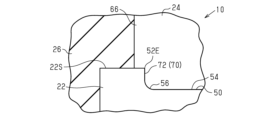
- FIG. 2 is a partially enlarged cross-sectional view of the nitride semiconductor device 10 of FIG.
- the gate layer 22 includes a trench 50 recessed in the upper surface 22S of the gate layer 22 in a region in contact with the gate electrode 24.
- Trench 50 includes a trench opening end 52E, a trench bottom surface 54, and a curved surface 56 that is continuous with trench bottom surface 54 and curves from trench bottom surface 54 toward trench opening end 52E.
- the shape of the trench 50 is not particularly limited, in the example of FIG. 2, the trench 50 is formed into a bowl shape when viewed in cross section.
- the trench opening end 52E of the trench 50 includes a first end 52EA and a second end 52EB that face each other in the first direction.
- the first direction is the direction in which the source electrode 32 (first opening 26A), gate layer 22, and drain electrode 34 (second opening 26B) are lined up in FIG. 1, and corresponds to the X direction in FIG. do.
- the trench 50 has a trench width W1 corresponding to the distance between the first end 52EA and the second end 52EB in the first direction, and the curved surface 56 of the trench 50 extends from the trench bottom surface 54 to the first end 52EB. It includes a first curved surface 56A that curves toward the end 52EA, and a second curved surface 56B that curves from the trench bottom surface 54 toward the second end 52EB.
- the gate electrode 24 has a gate electrode length L1 in the first direction.
- the trench 50 (gate layer 22) and the gate electrode 24 are configured such that the trench width W1 is equal to or less than the gate electrode length L1.
- the gate electrode 24 includes an upper electrode part 62 and a lower electrode part 64.
- the lower electrode portion 64 corresponds to the lower region of the gate electrode 24 filled in the trench 50 .
- the upper electrode portion 62 is formed integrally with the lower electrode portion 64 and corresponds to an upper region of the gate electrode 24 located above the position of the upper surface 22S of the gate layer 22.
- the trench width W1 is less than the gate electrode length L1.
- the upper electrode portion 62 includes a protrusion 66 that protrudes laterally from the trench opening end 52E along the upper surface 22S of the gate layer 22.
- the protrusion 66 includes a first protrusion 66A that protrudes laterally along the upper surface 22S of the gate layer 22 from the first end 52EA of the trench opening end 52E, and a first protrusion 66A that protrudes laterally along the upper surface 22S of the gate layer 22 from the second end 52EB of the trench opening end 52E. 22, and a second protrusion 66B that protrudes laterally along the upper surface 22S of 22.
- the gate electrode 24 includes a first electrode end 24EA and a second electrode end 24EB that are in contact with the upper surface 22S of the gate layer 22.
- the electrode end part 24E corresponds to the lower end of the side surface 66SA of the first protrusion 66A
- the second electrode end 24EB corresponds to the lower end of the side surface 66SB of the second protrusion 66B.
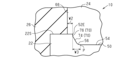
- FIG. 3 is a partially enlarged sectional view of FIG. 2.
- FIG. 4 is a partially enlarged sectional view showing possible structures of the gate electrode 24.
- the trench 50 has a depth D1
- the first curved surface 56A (curved surface 56) has a radius of curvature R1.
- FIG. 3 shows the first curved surface 56A, the same applies to the second curved surface 56B.
- the depth D1 corresponds to the distance from the trench opening end 52E to the trench bottom surface 54 in the direction perpendicular to the upper surface 22S of the gate layer 22.
- the upper electrode portion 62 of the gate electrode 24 has a first protrusion that protrudes laterally along the upper surface 22S of the gate layer 22 from the first end 52EA of the trench opening end 52E with a protrusion width W2. 66A. Therefore, the gate electrode 24 includes a first electrode end 24EA (electrode end 24E) that is in contact with the upper surface 22S of the gate layer 22.
- FIG. 3 shows the first protrusion 66A, the same applies to the second protrusion 66B.
- the depth D1 of the trench 50, the radius of curvature R1 of the curved surface 56, and the protrusion width W2 of the protrusion 66 are set to values that can alleviate local electric field concentration on the gate layer 22 by a combination of these parameters. obtain.
- the values of depth D1, radius of curvature R1, and protrusion width W2 are selected to provide a higher electric field relaxation effect than when using a typical gate layer without a trench structure. Note that the electric field relaxation effect when using the gate layer 22 having a trench structure (the trench 50 including the curved surface 56) will be described later.
- the depth D1 may be, for example, 10 nm or more and 50 nm or less
- the radius of curvature R1 may be, for example, 5 nm or more and 30 nm or less
- the protrusion width W2 may be, for example, greater than 0 and 100 nm or less.
- the depth D1, the radius of curvature R1, and the protrusion width W2 are not necessarily limited to these ranges, and may be set to other ranges in which the electric field relaxation effect can be obtained.
- FIG. 4 shows a structure in which the protrusion width W2 of the protrusion 66 is 0 nm (that is, when the gate electrode 24 does not include the protrusion 66). In this way, the gate electrode 24 does not need to include the protrusion 66.
- the side surface 62S of the upper electrode section 62 is flat and continuous with the outer surface 64S of the lower electrode section 64 at the trench opening end 52E (first end 52EA in FIG. 4). Therefore, the gate electrode 24 in FIG. 4 does not include the electrode end portion 24E of the gate electrode 24 in FIG.
- FIG. 5 is a diagram showing simulation results of the electric field distribution (equipotential lines) around the gate electrode 24 of the nitride semiconductor device 10 of FIG. 1. Note that the structure in FIG. 5 corresponds to the structure in FIG. 3. This simulation result shows the electric field distribution when a gate voltage of, for example, 10 V is applied to the gate electrode 24. As shown in FIG. 5, in the structure of the gate layer 22 having the trench 50, the electric field (equipotential line) is concentrated in the region F1 of the curved surface 56 of the trench 50 (first curved surface 56A in FIG. 5). .
- FIG. 6 is a diagram showing simulation results of the electric field distribution (equipotential lines) around the gate electrode 240 of a typical nitride semiconductor device 100 including a gate layer 220 without a trench structure. Note that the structure in FIG. 6 is shown as a comparative example with the structure in FIG. 5.
- Gate layer 220 includes a flat top surface 220S and does not have trench 50 as in FIG.
- the gate electrode 240 is provided on the upper surface 220S of the gate layer 220, and includes an electrode end 240E (first electrode end 240EA in FIG. 6) in contact with the upper surface 220S.
- the electric field is locally concentrated in the region F2 of the gate layer 220 near the electrode end 240E of the gate electrode 240. ing.
- the electric field applied to the gate layer 22 is relaxed compared to the structure of FIG. 6.
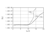
- FIG. 7 is a graph showing the gate breakdown voltage characteristics of the nitride semiconductor device 10 of FIG. 1 and the gate breakdown voltage characteristics of the nitride semiconductor device 100 of FIG. 6.
- a solid line graph 10L1 shows the gate breakdown voltage characteristics of the nitride semiconductor device 10
- a broken line graph 100L1 shows the gate breakdown voltage characteristics of the nitride semiconductor device 100.
- the horizontal axis represents the gate voltage Vg
- the vertical axis represents the gate current Ig.
- FIG. 8 is a graph showing the maximum electric field strength of the nitride semiconductor device 10 of FIG. 1 and the maximum electric field strength of the nitride semiconductor device 100 of FIG. 6.
- a solid line graph 10L2 indicates the maximum electric field intensity of the nitride semiconductor device 10
- a broken line graph 100L2 indicates the maximum electric field intensity of the nitride semiconductor device 100.
- the maximum electric field strength used in the present disclosure refers to the electric field strength at a location where the maximum electric field is applied.
- the two graphs 10L2 and 100L2 show that the maximum electric field strength (that is, the maximum applied electric field) is reduced in the nitride semiconductor device 10 of FIG. 1 compared to the nitride semiconductor device 100 of FIG. 6. .
- the maximum electric field is applied to the region F2 (near the electrode end 240E) of the gate layer 220 where the electric field is locally concentrated. Therefore, the graph 100L2 shows the electric field strength in the region F2 (near the electrode end 240E).
- the maximum electric field is applied to the region F1 (see FIG. 5) of the curved surface 56. Therefore, the graph 10L2 shows the electric field strength in the region F1 of the curved surface 56.
- the electric field applied to the gate layer 22 is dispersed and local electric field concentration is alleviated. As a result, in the nitride semiconductor device 10 of FIG. 1, the maximum electric field strength is reduced.
- the maximum electric field applied to the nitride semiconductor device 100 is approximately 5.69
- the maximum electric field applied to the nitride semiconductor device 10 is approximately 5.69
- the electric field is approximately 4.50. Therefore, an electric field relaxation effect is obtained.
- FIG. 9 shows the protrusion width W2 (see FIG. 3) of the protrusion 66 of the gate electrode 24, the depth D1 (see FIG. 3) of the trench 50, and the maximum electric field strength (the curved surface 56) in the nitride semiconductor device 10 of FIG. 2 is a graph showing the relationship between the maximum electric field applied to
- the example in FIG. 9 shows the relationship between the protrusion width W2 of the protrusion 66 and the maximum electric field applied to the curved surface 56 for three trenches 50 having depths D1 of 10 nm, 30 nm, and 50 nm, respectively.
- the gate voltage Vg is, for example, 10V.
- the protrusion width W2 is changed to, for example, 0 nm, 25 nm, 50 nm, 75 nm, 100 nm, 200 nm, and 250 nm.
- the reference value Ref indicates the maximum electric field strength of the nitride semiconductor device 100 in FIG. 6, that is, the maximum electric field (approximately 5.69) applied to the region F2 near the electrode end 240E.
- the maximum electric field strength becomes lower than the reference value Ref at a protrusion width W2 of 100 nm or less.
- the maximum electric field strength becomes lower than the reference value Ref regardless of the protrusion width W2.
- the protrusion width W2 is 100 nm or less, the maximum electric field strength will be lower than the reference value Ref regardless of the depth D1 of the trench 50.
- the gate electrode 24 includes the protrusion 66, the electric field relaxation effect is exhibited as long as the protrusion width W2 is greater than 0 and less than or equal to 100 nm, and the depth D1 is greater than or equal to 10 nm and less than or equal to 50 nm.
- the graph in FIG. 9 shows that the smaller the protrusion width W2, the greater the electric field relaxation effect. This is because as the protrusion width W2 increases, the distance between the electrode end 24E and the curved surface 56 increases, making it impossible to obtain a sufficient effect of alleviating electric field concentration near the electrode end 24E.
- the depth D1 is small, for example, when the depth D1 is 10 nm, the electric field relaxation effect is smaller than when the depth D1 is 30 nm or 50 nm. This is because the effect of widely dispersing the electric field using the curved surface 56 of the trench 50 is reduced. Therefore, the depth D1 is more preferably 30 nm or more and 50 nm or less.
- the maximum electric field strength is the highest regardless of whether the depth D1 of the trench 50 is 10 nm, 30 nm, or 50 nm. It gets lower. Therefore, by combining the structure of the gate electrode 24 shown in FIG. 4 described above with the trench structure of the gate layer 22, the maximum electric field relaxation effect can be obtained. Therefore, it is preferable that the gate electrode 24 has the structure shown in FIG. 4 rather than the structure shown in FIG.
- FIG. 10 shows the protrusion width W2 (see FIG. 3) of the protrusion 66 of the gate electrode 24, the radius of curvature R1 (see FIG. 3) of the curved surface 56, and the maximum electric field strength (see FIG. 3) in the nitride semiconductor device 10 of FIG. 56 is a graph showing the relationship between the maximum electric field applied to the
- the example in FIG. 10 shows the relationship between the protrusion width W2 of the protrusion 66 and the maximum electric field applied to the curved surface 56 for four trenches 50 in which the curved surface 56 has a radius of curvature R1 of 5 nm, 10 nm, 20 nm, and 30 nm, respectively. It shows a relationship.
- the gate voltage Vg is, for example, 10V.
- the protrusion width W2 is varied, for example, from 0 nm to 50 nm to 100 nm.
- the reference value Ref indicates the maximum electric field strength of the nitride semiconductor device 100 of FIG. 6, that is, the maximum electric field (approximately 5.69) applied to the region F2 near the electrode end 240E. There is.
- the maximum electric field strength becomes lower than the reference value Ref at a protrusion width W2 of 40 nm or less.
- the radius of curvature R1 is 10 nm, 20 nm, and 30 nm, the maximum electric field strength is lower than the reference value Ref regardless of the protrusion width W2. Therefore, when the gate electrode 24 includes the protrusion 66, the electric field relaxation effect is exhibited as long as the protrusion width W2 is greater than 0 and less than or equal to 100 nm, and the radius of curvature R1 is greater than or equal to 10 nm and less than or equal to 30 nm.
- the electric field relaxation effect is exhibited if the protrusion width W2 is greater than 0 and less than or equal to 40 nm, and the radius of curvature R1 is greater than or equal to 5 nm and less than or equal to 30 nm.
- FIG. 10 also shows that the smaller the protrusion width W2, the greater the electric field relaxation effect. This is because, as described above, when the protrusion width W2 increases, the distance between the electrode end 24E and the curved surface 56 increases, making it impossible to obtain a sufficient effect of alleviating electric field concentration near the electrode end 24E. It's for a reason. Further, when the radius of curvature R1 is small, for example, when the radius of curvature R1 is 5 nm, the electric field relaxation effect is smaller than when the radius of curvature R1 is 10 nm, 20 nm, or 30 nm. This is because when the curvature of the curved surface 56 is small, the electric field concentration on the curved surface 56 becomes large. Therefore, the radius of curvature R1 is more preferably 10 nm or more and 30 nm or less.
- Gate layer 22 of nitride semiconductor device 10 includes a trench 50 recessed in upper surface 22S of gate layer 22 in a region in contact with gate electrode 24.
- Trench 50 includes a curved surface 56 that curves from trench bottom surface 54 toward trench opening end 52E.
- the electric field is concentrated on a wider curved surface 56 of the trench 50, thereby suppressing local electric field concentration in the gate layer 22 near the electrode end 24E of the gate electrode 24.
- the electric field applied to the gate layer 22 is relaxed.
- the gate electrode 24 does not include the protrusion 66
- the gate electrode 24 does not include the electrode end portion 24E in contact with the upper surface 22S of the gate layer 22. Therefore, the electric field applied to the gate layer 22 is further relaxed.
- the nitride semiconductor device 10 of the first embodiment has the following advantages.
- (1-1) The gate layer 22 has a trench 50 including a curved surface 56. With this structure, the electric field can be concentrated over a wider range of curved surface 56 of trench 50. Thereby, local electric field concentration in the portion of the gate layer 22 near the electrode end 24E of the gate electrode 24 can be suppressed, and the electric field (maximum electric field strength) applied to the gate layer 22 can be relaxed. As a result, it is possible to suppress crystal defects in the gate layer that may occur due to local electric field concentration, as well as crystal destruction, and to suppress a decrease in gate breakdown voltage.
- the trench width W1 of the trench 50 is less than or equal to the gate electrode length L1 of the gate electrode 24 (see FIG. 2).
- the gate electrode 24 includes a lower electrode portion 64 filled in the trench 50 and an upper electrode portion 62 formed integrally with the lower electrode portion 64 and located above the top surface position of the gate layer 22. include.
- the gate electrode 24 may be configured such that the side surface 62S of the upper electrode section 62 includes a side surface 62S that is flat and continuous with the outer surface 64S of the lower electrode section 64 at the position of the trench opening end 52E (see FIG. 4).
- gate electrode 24 does not include protrusion 66 (see FIG. 3) and electrode end 24E (see FIG. 3).
- the upper electrode portion 62 may include a protrusion 66 that protrudes laterally from the trench opening end 52E along the upper surface 22S of the gate layer 22 (see FIG. 3). Even with such a structure of the gate electrode 24, the electric field applied to the gate layer 22 can be relaxed by using the gate layer 22 having the trench 50 including the curved surface 56.
- the protrusion 66 may protrude laterally from the trench opening end 52E along the upper surface 22S of the gate layer 22 with a protrusion width W2 that is less than or equal to the depth D1 of the trench 50. If the protrusion width W2 is large, the distance between the electrode end 24E and the curved surface 56 becomes large, so that the effect of alleviating electric field concentration near the electrode end 24E may not be sufficiently obtained. Since the protrusion width W2 is limited according to the depth D1 by satisfying the relationship W2 ⁇ D1, the electric field relaxation effect can be maintained satisfactorily.
- the protrusion width W2 of the protrusion 66 may be greater than 0 nm and less than or equal to 100 nm.
- the electric field relaxation effect is exhibited (see FIG. 9).
- the radius of curvature R1 of the curved surface 56 is exhibited (see FIG. 10). As shown in FIGS.
- the electron transit layer 16 may be a GaN layer.
- the electron supply layer 18 may be an AlGaN layer.
- the gate layer 22 may be a GaN layer containing acceptor type impurities. With this structure, it is possible to reduce the electric field (maximum electric field strength) applied to the gate layer 22 in a normally-off type GaN-HEMT, thereby suppressing a decrease in gate breakdown voltage.
- FIGS. 11 to 13 are schematic cross-sectional views of an exemplary nitride semiconductor device 10 according to the second embodiment. Note that in FIGS. 11 to 13, the same reference numerals are given to the same components as those of the nitride semiconductor device 10 according to the first embodiment. In the following, descriptions of components similar to those in the first embodiment will be omitted, and components different from those in the first embodiment will be described.
- the trench 50 includes a trench wall surface 70 that connects the trench opening end 52E and the curved surface 56.
- trench wall surface 70 includes a vertical surface 72 perpendicular to upper surface 22S of gate layer 22.
- the trench wall surface 70 includes an inclined surface 74 inclined with respect to the upper surface 22S of the gate layer 22.
- sloped surface 74 has an inclination angle of 60 degrees
- sloped surface 74 has a more gradual slope angle of 30 degrees.
- the slope 74 may be arbitrarily selected to be greater than 0° and less than 90°, but is preferably greater than or equal to 30° and less than or equal to 60°.
- the trench wall surface 70 may include a second curved surface 76 in addition to the inclined surface 74.
- the second curved surface 76 connects the inclined surface 74 and the trench opening end 52E.
- the second curved surface 76 can also have the effect of dispersing the electric field applied to the gate layer 22 and mitigating local electric field concentration.
- trench wall surface 70 may include only sloped surface 74.
- the trench 50 includes the trench wall surface 70 between the trench opening end 52E and the curved surface 56, the depth D1 of the trench 50 (see FIG. 3) and the radius of curvature R1 of the curved surface 56 (see FIG. 3) can be set as desired. It becomes easier to form the value of .
- the protrusion width W2 of the protrusion 66 is determined from the connection point P between the curved surface 56 and the trench bottom surface 54 to the trench opening end in a plan view.
- the distance W3 across the curved surface 56 up to 52E may be less than or equal to W3.
- the trench 50 in FIG. 13 may also be formed to satisfy the relationship W2 ⁇ W3.
- the trench 50 in FIG. 11 or the trench 50 in the first embodiment may also be formed to satisfy the relationship W2 ⁇ W3.
- Table 1 below shows the maximum force applied to the curved surface 56 when the protrusion width W2 of the protrusion 66 and the depth D1 of the trench 50 are changed in the trench 50 of FIG.
- the gate voltage is, for example, 10V
- the protrusion width W2 is varied between 0 nm, 50 nm, and 100 nm
- the depth D1 is varied between 10 nm, 30 nm, and 50 nm.
- the radius of curvature R1 of the curved surface 56 is, for example, 5 nm.
- Table 2 also shows that in the trench 50 of FIG. 12 which includes the slope 74 with an inclination angle of 60° as the trench wall surface 70, the protrusion width W2 of the protrusion 66 and the depth D1 of the trench 50 are changed under the same conditions as in Table 1.
- the figure shows an example in which the maximum electric field applied to the curved surface 56 was measured when the curved surface 56 was bent.
- Table 3 shows that in the trench 50 of FIG. 13 which includes the slope 74 with an inclination angle of 30° as the trench wall surface 70, the protrusion width W2 of the protrusion 66 and the depth D1 of the trench 50 are changed under the same conditions as Table 1.
- the figure shows an example in which the maximum electric field applied to the curved surface 56 was measured when the curved surface 56 was bent.
- Tables 1 to 1 The maximum electric field shown in Fig. 3 is lower than the reference value Ref when the protrusion width W2 is 0 nm. Further, depending on the combination of the protrusion width W2 and the depth D1, the maximum electric field becomes lower than the reference value Ref.
- the maximum electric field is lower when the slope is on the inclined surface 74 than when it is on the vertical surface 72, and the maximum electric field is lower when the slope angle of the slope 74 is 30° compared to when the slope is at 60°.
- the maximum electric field is lower when the slope angle of the slope 74 is 30° compared to when the slope is at 60°.
- the nitride semiconductor device 10 is configured as a normally-off type nitride semiconductor HEMT, but it may also be configured as a normally-on type nitride semiconductor HEMT.
- the nitride semiconductor device 10 is configured as a HEMT using gallium nitride, but it may be configured as a HEMT using other group III nitride semiconductors.
- the radius of curvature R1 of the curved surface 56 can also be changed as appropriate.
- the term “on” as used in this disclosure includes the meanings of “on” and “above” unless the context clearly indicates otherwise.
- the phrase “the first layer is formed on the second layer” refers to the fact that in some embodiments the first layer may be directly disposed on the second layer in contact with the second layer, but in other embodiments. It is contemplated that the first layer may be placed above the second layer without contacting the second layer. That is, the term “on” does not exclude structures in which other layers are formed between the first layer and the second layer.
- an intermediate layer for example, a spacer layer
- the electron supply layer 18 is formed on the electron transit layer 16
- an intermediate layer for example, a spacer layer
- the Z-axis direction used in the present disclosure does not necessarily have to be a vertical direction, nor does it need to completely coincide with the vertical direction. Accordingly, in various structures according to the present disclosure (e.g., the structure shown in FIG. 1), “upper” and “lower” in the Z-axis direction described herein are “upper” and “lower” in the vertical direction. Not limited to one thing.
- the X-axis direction may be a vertical direction
- the Y-axis direction may be a vertical direction.
- Appendix A1 an electron transit layer (16) made of a nitride semiconductor; A nitride semiconductor disposed on the electron transit layer (16) and having a larger band gap than the electron transit layer (16) to generate a two-dimensional electron gas (20) in the electron transit layer (16).
- the gate layer (22) includes a trench (50) recessed in the upper surface (22S) of the gate layer (22) in a region in contact with the gate electrode (24),
- the trench (50) is a trench opening end (52E), a trench bottom (54); a curved surface (56:56A; 56B) that is continuous with the trench bottom surface (54) and curves from the trench bottom surface (54) toward the trench opening end (52E);
- a nitride semiconductor device (10) comprising:
- the trench opening end (52E) includes a first end (52EA) and a second end (52EB) that face each other in the first direction,
- the trench (50) has a trench width (W1) corresponding to the distance between the first end (52EA) and the second end (52EB) in the first direction,
- the gate electrode (24) has a gate electrode length (L1) in the first direction,
- the gate electrode (24) is a lower electrode portion (64) filled in the trench (50); an upper electrode part (62) formed integrally with the lower electrode part (64) and located above the upper surface position of the gate layer (22);
- the upper electrode part (62) includes a side surface (62S) that is flat and continuous with the outer surface (64S) of the lower electrode part (64) at the position of the trench opening end (52E), according to appendix A1 or A2.
- the gate electrode (24) is a lower electrode portion (64) filled in the trench (50); an upper electrode part (62) formed integrally with the lower electrode part (64) and located above the upper surface position of the gate layer (22);
- the upper electrode portion (62) includes a protrusion (66:66A; 66B) that protrudes laterally from the trench opening end (52E) along the upper surface of the gate layer (22), as described in Appendix A1 or A2.
- the protrusion (66:66A; 66B) extends from the trench opening end (52E) along the upper surface of the gate layer (22) with a protrusion width (W2) equal to or less than the depth (D1) of the trench (50).
- the protrusion width (W2) is defined as the width of the curved surface (56) from the connection point (P) between the curved surface (56:56A; 56B) and the trench bottom surface (54) to the trench opening end (52E) in plan view. 56A;
- the protrusion (66:66A; 66B) protrudes laterally from the trench opening end (52E) along the upper surface of the gate layer (22) with a protrusion width (W2) of greater than 0 nm and less than or equal to 100 nm. , the nitride semiconductor device (10) according to appendix A4.
- the trench (50) includes a trench wall surface (70) connecting the trench opening end (52E) and the curved surface (56:56A; 56B), as described in any one of Appendices A1 to A6.
- the electron transit layer (16) is a GaN layer
- the electron supply layer (18) is an AlGaN layer.
- the nitride semiconductor device (10) according to any one of appendices A1 to A15, wherein the gate layer (22) is a GaN layer containing the acceptor type impurity.
Landscapes
- Engineering & Computer Science (AREA)
- Microelectronics & Electronic Packaging (AREA)
- Power Engineering (AREA)
- Physics & Mathematics (AREA)
- Condensed Matter Physics & Semiconductors (AREA)
- General Physics & Mathematics (AREA)
- Computer Hardware Design (AREA)
- Ceramic Engineering (AREA)
- Manufacturing & Machinery (AREA)
- Junction Field-Effect Transistors (AREA)
Abstract
窒化物半導体装置(10)は、電子走行層(16)と、電子走行層(16)上に配置された電子供給層(18)と、電子供給層(18)上に配置されたゲート層(22)と、ゲート層(22)と接するゲート電極(24)と、電子走行層(16)における二次元電子ガス(20)に電気的に接続されたソース電極(32)およびドレイン電極(34)とを備える。ゲート層(22)は、ゲート電極(24)と接する領域においてゲート層(22)の上面(22S)に凹設されたトレンチ(50)を含む。トレンチ(50)は、トレンチ開口端(52E)と、トレンチ底面(54)と、トレンチ底面(54)に連続するとともにトレンチ底面(54)からトレンチ開口端(52E)に向けて湾曲する湾曲面(56)とを含む。
Description
本開示は、窒化物半導体装置に関する。
現在、窒化ガリウム(GaN)等のIII族窒化物半導体(以下、単に「窒化物半導体」と言う場合がある)を用いた高電子移動度トランジスタ(HEMT)の製品化が進んでいる。HEMTは、半導体ヘテロ接合の界面付近に形成された二次元電子ガス(2DEG)を導電経路(チャネル)として使用する。HEMTを利用したパワーデバイスは、典型的なシリコン(Si)パワーデバイスと比較して低オン抵抗および高速・高周波動作を可能にしたデバイスとして認知されている。
例えば、窒化物半導体HEMTは、窒化ガリウム(GaN)層によって構成された電子走行層と、窒化アルミニウムガリウム(AlGaN)層によって構成された電子供給層とを含む。これら電子走行層と電子供給層とのヘテロ接合の界面付近において電子走行層中に2DEGが形成される。また、ノーマリーオフ型HEMTの場合、例えば、アクセプタ型不純物を含む半導体層(例えばp型GaN層)がゲート電極の直下において電子走行層上にゲート層として設けられる。この構成では、ゲート層から下方に広がる空乏層によりゲート層の直下のチャネルが消失することで、ノーマリーオフが実現される。特許文献1は、このようなノーマリーオフ型の窒化物半導体HEMTを開示している。
窒化物半導体HEMTでは、例えば、ゲート電極への正電圧の印加時にゲート電極端部付近のゲート層の部分に電界が局所的に集中する。このような局所的な電界集中は、ゲート層の結晶欠陥ひいては結晶破壊をもたらしてゲート耐圧を低下させる要因となり得る。したがって、局所的な電界集中を緩和することが求められている。
本開示の一態様による窒化物半導体装置は、窒化物半導体によって構成された電子走行層と、前記電子走行層に二次元電子ガスを発生させるべく前記電子走行層上に配置されるとともに前記電子走行層よりも大きなバンドギャップを有する窒化物半導体によって構成された電子供給層と、前記電子供給層上に配置されるとともにアクセプタ型不純物を含む窒化物半導体によって構成されたゲート層と、前記ゲート層と接するゲート電極と、前記二次元電子ガスに電気的に接続されたソース電極およびドレイン電極とを備える。前記ゲート層は、前記ゲート電極と接する領域において前記ゲート層の上面に凹設されたトレンチを含む。前記トレンチは、トレンチ開口端と、トレンチ底面と、前記トレンチ底面に連続するとともに前記トレンチ底面から前記トレンチ開口端に向けて湾曲する湾曲面とを含む。
本開示の一態様による窒化物半導体装置は、局所的な電界集中を緩和することができる。
以下、添付図面を参照して本開示による半導体装置のいくつかの実施形態を説明する。なお、図面に示される構成要素は、分かり易さおよび明瞭化のために部分的に拡大されている場合があり、必ずしも一定の縮尺で描かれていない。また、理解を容易にするために、断面図では、ハッチング線が省略されている場合がある。添付の図面は、本開示の実施形態を例示するに過ぎず、本開示を制限するものとみなされるべきではない。
以下の詳細な記載は、本開示の例示的な実施形態を具体化する装置、システム、および方法を含む。この詳細な記載は本来説明のためのものに過ぎず、本開示の実施形態またはこのような実施形態の適用および使用を限定することを意図しない。
[第1実施形態]
図1は、第1実施形態に係る例示的な窒化物半導体装置10の概略断面図である。まず図1を参照して、窒化物半導体装置10の全体構造を以下に説明する。
図1は、第1実施形態に係る例示的な窒化物半導体装置10の概略断面図である。まず図1を参照して、窒化物半導体装置10の全体構造を以下に説明する。
[窒化物半導体装置の全体構造]
窒化物半導体装置10は、例えば、窒化ガリウム(GaN)等の窒化物半導体を用いた高電子移動度トランジスタ(HEMT)として構成され得る。窒化物半導体装置10は、基板12と、基板12上に形成されたバッファ層14と、バッファ層14上に形成された電子走行層16と、電子走行層16上に形成された電子供給層18とを含む。
窒化物半導体装置10は、例えば、窒化ガリウム(GaN)等の窒化物半導体を用いた高電子移動度トランジスタ(HEMT)として構成され得る。窒化物半導体装置10は、基板12と、基板12上に形成されたバッファ層14と、バッファ層14上に形成された電子走行層16と、電子走行層16上に形成された電子供給層18とを含む。
基板12は、シリコン(Si)、シリコンカーバイド(SiC)、窒化アルミニウム(AlN)、GaN、サファイア、または他の基板材料で形成され得る。例えば、基板12は、Si基板である。基板12の厚さは、例えば、200μm以上1500μm以下であってよい。なお、図1に示される互いに直交するXYZ軸のZ方向は、基板12の主面と直交する方向である。本明細書において使用される「平面視」という用語は、明示的に別段の記載がない限り、Z方向に沿って上方から窒化物半導体装置10を視ることをいう。
バッファ層14は、基板12と電子走行層16との間に位置し、基板12と電子走行層16との間の格子不整合を緩和することができる任意の材料によって形成され得る。例えば、バッファ層14は、1つまたは複数の窒化物半導体層を含む。例えば、バッファ層14は、AlN層、窒化アルミニウムガリウム(AlGaN)層、および異なるアルミニウム(Al)組成を有するグレーテッドAlGaN層のうちの少なくとも1つを含み得る。例えば、バッファ層14は、単一のAlN層、単一のAlGaN層、AlGaN/GaN超格子構造を有する層、AlN/AlGaN超格子構造を有する層、またはAlN/GaN超格子構造を有する層によって形成され得る。
一例において、バッファ層14は、基板12上に形成された第1バッファ層と、第1バッファ層上に形成された第2バッファ層とを含む。第1バッファ層は、例えばAlN層であり、例えば200nm程度の厚さを有し得る。第2バッファ層は、例えば複数のAlGaN層を含み、各AlGaN層は例えば100nm程度の厚さを有し得る。なお、バッファ層14におけるリーク電流を抑制するために、バッファ層14の一部に不純物を導入して半絶縁性にしてもよい。その場合、不純物は、例えば炭素(C)または鉄(Fe)であり、不純物の濃度は、例えば4×1016cm-3以上であってよい。
電子走行層16は、窒化物半導体によって構成されており、例えばGaN層であってよい。電子走行層16は、例えば0.5μm以上2μm以下の厚さを有し得る。なお、電子走行層16におけるリーク電流を抑制するために、電子走行層16の一部に不純物を導入して電子走行層16の表層領域以外を半絶縁性にしてもよい。その場合、不純物は例えばCであり、不純物の濃度は、例えばピーク濃度で1×1019cm-3以上であってよい。
電子供給層18は、電子走行層16よりも大きなバンドギャップを有する窒化物半導体によって構成されており、例えばAlGaN層であってよい。AlGaN層の場合、Al組成が大きいほどバンドギャップが大きくなるため、AlGaN層である電子供給層18は、GaN層である電子走行層16よりも大きなバンドギャップを有している。例えば、電子供給層18はAlxGa1-xNによって構成されており、必ずしも限定されないが、xは0.1<x<0.4であり、より好ましくは0.2<x<0.3である。電子供給層18は、例えば5nm以上20nm以下の厚さを有し得る。
電子走行層16と電子供給層18は、互いに異なる格子定数を有する窒化物半導体によって構成されている。したがって、電子走行層16を構成する窒化物半導体(例えば、GaN)と電子供給層18を構成する窒化物半導体(例えば、AlGaN)とは格子不整合系の接合になっている。電子走行層16および電子供給層18の自発分極と、電子供給層18のヘテロ接合部が受ける応力に起因するピエゾ分極とによって、電子走行層16と電子供給層18とのヘテロ接合界面付近における電子走行層16の伝導帯のエネルギーレベルはフェルミ準位よりも低くなる。これにより、電子走行層16と電子供給層18とのヘテロ接合界面に近い位置(例えば、界面から数nm程度の距離)において電子走行層16内には二次元電子ガス(2DEG)20が広がっている。
窒化物半導体装置10はさらに、電子供給層18上に形成されたゲート層22と、ゲート層22上に形成されたゲート電極24と、パッシベーション層26とを含む。パッシベーション層26は、電子供給層18、ゲート層22、およびゲート電極24を被覆している。
ゲート層22は、アクセプタ型不純物を含む窒化物半導体によって電子供給層18上に形成されている。ゲート層22は、電子供給層18よりも小さなバンドギャップを有する任意の材料によって構成され得る。例えば、電子供給層18がAlGaN層である場合、ゲート層22は、アクセプタ型不純物がドープされたGaN層、すなわちp型GaN層であってよい。アクセプタ型不純物は、例えば、亜鉛(Zn)、マグネシウム(Mg)、および炭素(C)のうちの少なくとも1つを含み得る。アクセプタ型不純物は、例えば、7×1018cm-3以上1×1020cm-3以下の最大濃度を有し得る。
ゲート電極24は、ゲート層22とショットキー接合を形成している。ゲート電極24は、1つまたは複数の金属層によって構成されており、例えば窒化チタン(TiN)層であってよい。あるいは、ゲート電極24は、第1金属層(例えば、Ti層)と、第1金属層上に設けられた第2金属層(例えば、TiN層)とによって構成されてもよい。ゲート層22の上面22Sからゲート電極24の上面までのゲート電極24の厚さは、例えば、50nm以上300nm以下であってよい。ゲート電極24の直下にアクセプタ型不純物を含む窒化物半導体層がゲート層22として設けられた構造では、ゲート層22に含まれるアクセプタ型不純物の存在によって電子走行層16のチャネル(2DEG20)が消失する。これにより、ノーマリーオフ型の窒化物半導体HEMTが実現されている。
パッシベーション層26は、例えば、窒化シリコン(SiN)膜、二酸化シリコン(SiO2)膜、酸窒化シリコン(SiON)膜、アルミナ(Al2O3)膜、AlN膜、および酸窒化アルミニウム(AlON)膜のうちのいずれか1つの単膜か、またはそれらの2つ以上の任意の組み合わせを含む複合膜によって構成されている。
パッシベーション層26は、電子供給層18の上面をソース接続領域18Aとして露出させる第1開口部26Aと、電子供給層18の上面をドレイン接続領域18Bとして露出させる第2開口部26Bとを含む。ゲート層22は、第1開口部26Aと第2開口部26Bとの間に位置している。
窒化物半導体装置10はさらに、ソース電極32とドレイン電極34とを含む。ソース電極32は、パッシベーション層26の第1開口部26Aを介して電子供給層18のソース接続領域18Aに接しており、電子供給層18の直下の2DEG20にオーミック接触している。ドレイン電極34は、パッシベーション層26の第2開口部26Bを介して電子供給層18のドレイン接続領域18Bに接しており、電子供給層18の直下の2DEG20にオーミック接触している。
ソース電極32およびドレイン電極34は、例えば、Ti層、TiN層、Al層、AlSiCu層、およびAlCu層のうちの少なくとも1つを用いた1つまたは複数の金属層によって構成されている。例えば、ソース電極32およびドレイン電極34は、同じ材料で形成されている。
図1に示されるように、ゲート層22は、必ずしもこの構成に限定されないが、ステップ構造を有し得る。一例では、ゲート層22は、リッジ部42と、リッジ部42の両側から互いに反対方向に延在するソース側延在部44およびドレイン側延在部46とを含む。これらリッジ部42、ソース側延在部44、およびドレイン側延在部46によってゲート層22のステップ構造が形成されている。
リッジ部42は、ゲート層22の相対的に厚い部分に相当する。ゲート電極24は、リッジ部42に接している。リッジ部42は、図1のXZ平面に沿った断面において矩形状または台形状を有し得る。リッジ部42は、例えば100nm以上200nm以下の厚さを有し得る。リッジ部42の厚さとは、リッジ部42の上面から下面(電子供給層18に接するゲート層22の下面)までの距離のことである。リッジ部42(ゲート層22)の厚さは、ゲート耐圧などの種々のパラメータを考慮して決定され得る。
ソース側延在部44は、リッジ部42からパッシベーション層26の第1開口部26Aに向かって(図1において-X方向に)延在している。ドレイン側延在部46は、リッジ部42からパッシベーション層26の第2開口部26Bに向かって(図1において+X方向に)延在している。図1の例では、ドレイン側延在部46は、ソース側延在部44よりもリッジ部42から長く延びている。ただし、ソース側延在部44とドレイン側延在部46は同じ長さであってもよい。ソース側延在部44は、リッジ部42から第1開口部26Aに向かう方向において、例えば0.2μm以上0.3μm以下の長さを有し得る。ドレイン側延在部46は、リッジ部42から第2開口部26Bに向かう方向において、例えば0.2μm以上0.6μm以下の長さを有し得る。ソース側延在部44およびドレイン側延在部46は、例えば5nm以上30nm以下の厚さを有し得る。
ソース電極32の一部は、パッシベーション層26の第1開口部26A内に充填されており、ドレイン電極34の一部は、パッシベーション層26の第2開口部26B内に充填されている。
ソース電極32は、必ずしもこの構成に限定されないが、ソース電極部32Aと、ソース電極部32Aに連続するソースフィールドプレート部32Bとを含み得る。ソース電極部32Aは、第1開口部26Aに充填された充填領域と、充填領域と一体に形成されるとともに平面視において第1開口部26Aの周辺に位置する上部領域とを含む。ソースフィールドプレート部32Bは、ソース電極部32Aの上部領域と一体に形成されており、平面視においてゲート層22の全体(図1の例では、リッジ部42、ソース側延在部44、およびドレイン側延在部46の全て)を覆うようにパッシベーション層26上に設けられている。
ソースフィールドプレート部32Bは、ドレイン電極34の近傍に端部32Cを有している。この端部32Cは、平面視においてドレイン電極34とドレイン側延在部46との間に位置している。ソースフィールドプレート部32Bは、ゲート-ソース間電圧が0Vの状態でソース-ドレイン間に高電圧が印加された際に、ソースフィールドプレート部32Bの直下の2DEG20に向けて空乏層を伸ばすことで、ゲート電極24の端部付近およびゲート層22の端部近傍の電界集中を緩和する役割を果たす。
[トレンチを有するゲート層およびゲート電極の例示的な構造]
図2は、図1の窒化物半導体装置10の部分拡大断面図である。
図2に示されるように、ゲート層22は、ゲート電極24と接する領域においてゲート層22の上面22Sに凹設されたトレンチ50を含む。トレンチ50は、トレンチ開口端52Eと、トレンチ底面54と、トレンチ底面54に連続するとともにトレンチ底面54からトレンチ開口端52Eに向けて湾曲する湾曲面56とを含む。トレンチ50の形状は特に限定されないが、図2の例では、トレンチ50は断面視ボウル(bowl)状に形成されている。
図2は、図1の窒化物半導体装置10の部分拡大断面図である。
図2に示されるように、ゲート層22は、ゲート電極24と接する領域においてゲート層22の上面22Sに凹設されたトレンチ50を含む。トレンチ50は、トレンチ開口端52Eと、トレンチ底面54と、トレンチ底面54に連続するとともにトレンチ底面54からトレンチ開口端52Eに向けて湾曲する湾曲面56とを含む。トレンチ50の形状は特に限定されないが、図2の例では、トレンチ50は断面視ボウル(bowl)状に形成されている。
トレンチ50のトレンチ開口端52Eは、第1方向において互いに対向する第1端部52EAと第2端部52EBとを含む。第1方向とは、図1においてソース電極32(第1開口部26A)、ゲート層22、およびドレイン電極34(第2開口部26B)が並ぶ方向のことであり、図1におけるX方向に相当する。トレンチ50は、第1方向における第1端部52EAと第2端部52EBとの間の距離に相当するトレンチ幅W1を有しており、トレンチ50の湾曲面56は、トレンチ底面54から第1端部52EAに向けて湾曲する第1湾曲面56Aと、トレンチ底面54から第2端部52EBに向けて湾曲する第2湾曲面56Bとを含む。ゲート電極24は、第1方向にゲート電極長L1を有している。トレンチ50(ゲート層22)およびゲート電極24は、トレンチ幅W1がゲート電極長L1以下となるように構成されている。
ゲート電極24は、上部電極部62と、下部電極部64とを含む。下部電極部64は、トレンチ50内に充填されたゲート電極24の下部領域に相当する。上部電極部62は、下部電極部64と一体に形成されかつゲート層22の上面22Sの位置よりも上方に位置するゲート電極24の上部領域に相当する。
図2の例では、トレンチ幅W1はゲート電極長L1未満である。この場合、上部電極部62は、ゲート層22の上面22Sに沿ってトレンチ開口端52Eから側方に突出する突出部66を含む。突出部66は、トレンチ開口端52Eの第1端部52EAからゲート層22の上面22Sに沿って側方に突出する第1突出部66Aと、トレンチ開口端52Eの第2端部52EBからゲート層22の上面22Sに沿って側方に突出する第2突出部66Bとを含む。
したがって、図2の例では、ゲート電極24は、ゲート層22の上面22Sに接する第1電極端部24EAと第2電極端部24EBとを含む。なお、以下では、第1電極端部24EAと第2電極端部24EBとを区別しない場合は、それらをまとめて電極端部24Eと言う。第1電極端部24EAは、第1突出部66Aの側面66SAの下端部に相当し、第2電極端部24EBは、第2突出部66Bの側面66SBの下端部に相当する。
以下、図3および図4を参照して、トレンチ50(ゲート層22)とゲート電極24との構造上の関係について説明する。図3は、図2の部分拡大断面図である。図4は、ゲート電極24のとり得る構造を示す部分拡大断面図である。
図3に示されるように、トレンチ50は深さD1を有し、第1湾曲面56A(湾曲面56)は曲率半径R1を有している。なお、図3は第1湾曲面56Aについて示しているが、第2湾曲面56Bについても同様である。深さD1は、ゲート層22の上面22Sに直交する方向においてトレンチ開口端52Eからトレンチ底面54までの距離に相当する。
また、図3の例では、ゲート電極24の上部電極部62は、トレンチ開口端52Eの第1端部52EAからゲート層22の上面22Sに沿って側方に突出幅W2で突出する第1突出部66Aを含む。したがって、ゲート電極24は、ゲート層22の上面22Sに接する第1電極端部24EA(電極端部24E)を含む。なお、図3は第1突出部66Aについて示しているが、第2突出部66Bについても同様である。
トレンチ50の深さD1、湾曲面56の曲率半径R1、および突出部66の突出幅W2は、それらパラメータの組み合わせによってゲート層22への局所的な電界集中を緩和することができる値に設定され得る。例えば、深さD1、曲率半径R1、および突出幅W2の値は、トレンチ構造を有さない典型的なゲート層を用いた場合よりも高い電界緩和効果が得られるように選択される。なお、トレンチ構造(湾曲面56を含むトレンチ50)を有するゲート層22を用いた場合の電界緩和効果については後で説明する。
一例では、深さD1は例えば10nm以上50nm以下であってよく、曲率半径R1は例えば5nm以上30nm以下であってよく、突出幅W2は例えば0よりも大きく100nm以下であってよい。ただし、深さD1、曲率半径R1、および突出幅W2は、必ずしもこれらの範囲に限定されるものではなく、電界緩和効果が得られる他の範囲に設定されてもよい。
図4は、突出部66の突出幅W2が0nm(すなわち、ゲート電極24が突出部66を含まない場合)の構造を示している。このように、ゲート電極24は突出部66を含まなくてもよい。この構造では、上部電極部62の側面62Sが、トレンチ開口端52E(図4では第1端部52EA)の位置で下部電極部64の外面64Sと平坦に連続する。したがって、図4のゲート電極24は、図3のゲート電極24の電極端部24Eを含まない。
[トレンチ構造によって得られる電界緩和効果]
次に、トレンチ構造(湾曲面56を含むトレンチ50)を有するゲート層22を用いた場合に得られる電界緩和効果について説明する。
次に、トレンチ構造(湾曲面56を含むトレンチ50)を有するゲート層22を用いた場合に得られる電界緩和効果について説明する。
図5は、図1の窒化物半導体装置10のゲート電極24周辺の電界分布(等電位線)のシミュレーション結果を示す図である。なお、図5の構造は、図3の構造に対応する。このシミュレーション結果は、例えば10Vのゲート電圧をゲート電極24に印加した場合の電界分布を示している。図5に示されるように、トレンチ50を有するゲート層22の構造では、トレンチ50の湾曲面56(図5では第1湾曲面56A)の領域F1に電界(等電位線)が集中している。
図6は、トレンチ構造を有さないゲート層220を備えた典型的な窒化物半導体装置100のゲート電極240周辺の電界分布(等電位線)のシミュレーション結果を示す図である。なお、図6の構造は、図5の構造との比較例として示されている。ゲート層220は平坦な上面220Sを含み、図5のようなトレンチ50を有していない。ゲート電極240はゲート層220の上面220Sに設けられており、上面220Sに接する電極端部240E(図6では第1電極端部240EA)を含む。図6に示されるように、トレンチ構造を有さないゲート層220の構造では、ゲート電極240の電極端部240E付近のゲート層220の領域F2に電界(等電位線)が局所的に集中している。
ゲート層220の領域F2(電極端部240E付近)に局所的に電界が集中する図6の構造と比べて、図5の構造では、電極端部24E付近のゲート層22の領域における電界集中は殆ど生じておらず、より広範囲の湾曲面56の領域F1に電界が集中している。したがって、図6の構造と比べて、図5の構造では、ゲート層22にかかる電界が緩和されている。
図7は、図1の窒化物半導体装置10のゲート耐圧特性と図6の窒化物半導体装置100のゲート耐圧特性とを示すグラフである。なお、図7において、実線のグラフ10L1は、窒化物半導体装置10のゲート耐圧特性を示しており、波線のグラフ100L1は、窒化物半導体装置100のゲート耐圧特性を示している。また、横軸はゲート電圧Vg、縦軸はゲート電流Igを示している。
グラフ100L1で示されるように、図6の窒化物半導体装置100(トレンチ構造を有さないゲート層220)では、ゲート電圧Vgが約13V程度のときにブレークダウンが生じている。これに対し、グラフ10L1で示されるように、図1の窒化物半導体装置100(湾曲面56を含むトレンチ50を有するゲート層22)では、ゲート電圧Vgが増加するにつれてゲート電流Igが増加するものの、明らかなブレークダウンは見られない。さらには、ゲート電流Igの増加の割合も減少している。したがって、図1の窒化物半導体装置10では、図6の窒化物半導体装置100に比べてゲート耐圧特性が向上している。
図8は、図1の窒化物半導体装置10の最大電界強度と図6の窒化物半導体装置100の最大電界強度とを示すグラフである。図8において、実線のグラフ10L2は、窒化物半導体装置10の最大電界強度を示しており、波線のグラフ100L2は、窒化物半導体装置100の最大電界強度を示している。なお、本開示で使用される最大電界強度とは、最大電界が印加された箇所の電界強度を指す。
2つのグラフ10L2,100L2は、図6の窒化物半導体装置100に比べて、図1の窒化物半導体装置10では最大電界強度(すなわち、印加される最大電界)が低減されることを示している。上記のように、図6の窒化物半導体装置100では、電界が局所的に集中するゲート層220の領域F2(電極端部240E付近)に最大電界が印加される。したがって、グラフ100L2は、領域F2(電極端部240E付近)の電界強度を示している。
これに対して、図1の窒化物半導体装置10では、湾曲面56の領域F1(図5参照)に最大電界が印加される。したがって、グラフ10L2は、湾曲面56の領域F1の電界強度を示している。窒化物半導体装置10では、湾曲面56の領域F1に最大電界が印加されるため、ゲート層22にかかる電界が分散されて局所的な電界集中が緩和される。その結果、図1の窒化物半導体装置10では、最大電界強度が低減される。例えば、ゲート電圧Vgが10Vのとき、窒化物半導体装置100(領域F2)に印加される最大電界は約5.69であるのに対し、窒化物半導体装置10(領域F1)に印加される最大電界は約4.50である。したがって、電界緩和効果が得られている。
[ゲート電極突出幅とトレンチ深さと最大電界強度との関係]
図9は、図1の窒化物半導体装置10において、ゲート電極24の突出部66の突出幅W2(図3参照)とトレンチ50の深さD1(図3参照)と最大電界強度(湾曲面56に印加される最大電界)との関係を示すグラフである。
図9は、図1の窒化物半導体装置10において、ゲート電極24の突出部66の突出幅W2(図3参照)とトレンチ50の深さD1(図3参照)と最大電界強度(湾曲面56に印加される最大電界)との関係を示すグラフである。
図9の例は、それぞれ10nm、30nm、および50nmの深さD1を有する3つのトレンチ50について、突出部66の突出幅W2と湾曲面56に印加される最大電界との関係を示している。ゲート電圧Vgは例えば10Vである。また、突出幅W2は、例えば0nm、25nm、50nm、75nm、100nm、200nm、および250nmで変化させている。基準値Refは、図6の窒化物半導体装置100の最大電界強度、すなわち、電極端部240E付近の領域F2に印加された最大電界(約5.69)を示している。
図9に示されるように、トレンチ50の深さD1が10nmの場合、最大電界強度は、100nm以下の突出幅W2で基準値Refよりも低くなる。一方、トレンチ50の深さD1が30nmの場合および50nmの場合には、最大電界強度は、突出幅W2によらずに基準値Refよりも低くなる。言い換えれば、突出幅W2が100nm以下であれば、最大電界強度は、トレンチ50の深さD1によらずに基準値Refよりも低くなる。したがって、ゲート電極24が突出部66を含む場合には、突出幅W2が0よりも大きく100nm以下であり、かつ深さD1が10nm以上50nm以下であれば、電界緩和効果が発揮される。
ここで、図9のグラフは、突出幅W2が小さいほど、電界緩和効果が大きくなることを示している。これは、突出幅W2が大きくなると、電極端部24Eと湾曲面56との離間距離が大きくなることで電極端部24E付近の電界集中を緩和する効果が十分に得られなくなるためである。また、深さD1が小さい場合、例えば、深さD1が10nmの場合には、深さD1が30nmまたは50nmの場合と比べて電界緩和効果が小さくなる。これは、トレンチ50の湾曲面56を利用して電界を広範囲に分散させる効果が小さくなるためである。したがって、深さD1は、より好ましくは30nm以上50nm以下である。
また、突出幅W2が0nmの場合、すなわち、ゲート電極24が突出部66を含まない場合には、トレンチ50の深さD1が10nm、30nm、および50nmのいずれであっても最大電界強度が最も低くなる。このため、上述した図4のゲート電極24の構造をゲート層22のトレンチ構造と組み合わせることで、最大の電界緩和効果が得られる。したがって、ゲート電極24は、図5の構造よりも図4の構造であることが望ましい。
[ゲート電極突出幅と湾曲面の曲率と最大電界強度との関係]
図10は、図1の窒化物半導体装置10において、ゲート電極24の突出部66の突出幅W2(図3参照)と湾曲面56の曲率半径R1(図3参照)と最大電界強度(湾曲面56に印加される最大電界)との関係を示すグラフである。
図10は、図1の窒化物半導体装置10において、ゲート電極24の突出部66の突出幅W2(図3参照)と湾曲面56の曲率半径R1(図3参照)と最大電界強度(湾曲面56に印加される最大電界)との関係を示すグラフである。
図10の例は、湾曲面56がそれぞれ5nm、10nm、20nm、および30nmの曲率半径R1を有する4つのトレンチ50について、突出部66の突出幅W2と湾曲面56に印加される最大電界との関係を示している。ゲート電圧Vgは例えば10Vである。また、突出幅W2は、例えば0nm、50nm、100nmで変化させている。なお、図9と同様、基準値Refは、図6の窒化物半導体装置100の最大電界強度、すなわち、電極端部240E付近の領域F2に印加された最大電界(約5.69)を示している。
図10に示されるように、曲率半径R1が5nmの場合、最大電界強度は40nm以下の突出幅W2で基準値Refよりも低くなる。一方、曲率半径R1が10nmの場合、20nmの場合、および30nmの場合には、最大電界強度は、突出幅W2によらずに基準値Refよりも低くなる。したがって、ゲート電極24が突出部66を含む場合には、突出幅W2が0よりも大きく100nm以下であり、かつ曲率半径R1が10nm以上30nm以下であれば、電界緩和効果が発揮される。あるいは、ゲート電極24が突出部66を含む場合には、突出幅W2が0よりも大きく40nm以下であり、かつ曲率半径R1が5nm以上30nm以下であれば、電界緩和効果が発揮される。
なお、図10も、突出幅W2が小さいほど、電界緩和効果が大きくなることを示している。これは、上記したように、突出幅W2が大きくなると、電極端部24Eと湾曲面56との離間距離が大きくなることで電極端部24E付近の電界集中を緩和する効果が十分に得られなくなるためである。また、曲率半径R1が小さい場合、例えば、曲率半径R1が5nmの場合には、曲率半径R1が10nm、20nm、または30nmの場合と比べて電界緩和効果が小さくなる。これは、湾曲面56の曲率が小さいと、湾曲面56における電界集中が大きくなるためである。したがって、曲率半径R1は、より好ましくは10nm以上30nm以下である。
[窒化物半導体装置の作用]
次に、窒化物半導体装置10の作用について説明する。
窒化物半導体装置10のゲート層22は、ゲート電極24と接する領域においてゲート層22の上面22Sに凹設されたトレンチ50を含む。トレンチ50は、トレンチ底面54からトレンチ開口端52Eに向けて湾曲する湾曲面56を含む。この構造では、トレンチ50のより広範囲の湾曲面56に電界が集中することで、ゲート電極24の電極端部24E付近のゲート層22における局所的な電界集中が抑制される。その結果、ゲート層22にかかる電界が緩和される。特に、ゲート電極24が突出部66を含まない図4の構造の場合、ゲート電極24は、ゲート層22の上面22Sに接する電極端部24Eを含まない。このため、ゲート層22にかかる電界がより一層緩和される。
第1実施形態の窒化物半導体装置10は、以下の利点を有する。
(1-1)ゲート層22は、湾曲面56を含むトレンチ50を有する。この構造では、トレンチ50のより広範囲の湾曲面56に電界を集中させることができる。これにより、ゲート電極24の電極端部24E付近のゲート層22の部分における局所的な電界集中を抑制してゲート層22にかかる電界(最大電界強度)を緩和することができる。その結果、局所的な電界集中によって生じ得るゲート層の結晶欠陥ひいては結晶破壊を抑制して、ゲート耐圧の低下を抑制することができる。
(1-1)ゲート層22は、湾曲面56を含むトレンチ50を有する。この構造では、トレンチ50のより広範囲の湾曲面56に電界を集中させることができる。これにより、ゲート電極24の電極端部24E付近のゲート層22の部分における局所的な電界集中を抑制してゲート層22にかかる電界(最大電界強度)を緩和することができる。その結果、局所的な電界集中によって生じ得るゲート層の結晶欠陥ひいては結晶破壊を抑制して、ゲート耐圧の低下を抑制することができる。
(1-2)トレンチ50のトレンチ幅W1は、ゲート電極24のゲート電極長L1以下である(図2参照)。この構造では、ゲート層22にゲート電極24が接触する面積が減少することを抑制してゲート電極24からゲート層22にゲート信号を伝達する能力を良好に維持することができる。
(1-3)ゲート電極24は、トレンチ50に充填された下部電極部64と、下部電極部64と一体に形成されかつゲート層22の上面位置よりも上方に位置する上部電極部62とを含む。この場合、ゲート電極24は、上部電極部62の側面62Sがトレンチ開口端52Eの位置で下部電極部64の外面64Sと平坦に連続する側面62Sを含むように構成されてもよい(図4参照)。この構造では、ゲート電極24は突出部66(図3参照)および電極端部24E(図3参照)を含まない。このようなゲート電極24を、湾曲面56を含むトレンチ50を有するゲート層22と組み合わせることによって、ゲート層22にかかる電界をより一層緩和することができる。
(1-4)あるいは、上部電極部62は、ゲート層22の上面22Sに沿ってトレンチ開口端52Eから側方に突出する突出部66を含むものでもよい(図3参照)。このようなゲート電極24の構造でも、湾曲面56を含むトレンチ50を有するゲート層22を用いることによってゲート層22にかかる電界を緩和することができる。
(1-5)突出部66は、トレンチ50の深さD1以下の突出幅W2でゲート層22の上面22Sに沿ってトレンチ開口端52Eから側方に突出するものであってよい。突出幅W2が大きいと、電極端部24Eと湾曲面56との離間距離が大きくなることで電極端部24E付近の電界集中を緩和する効果が十分に得られなくなることがある。W2≦D1の関係が満たされることで突出幅W2が深さD1に応じて制限されるため、電界緩和効果を良好に維持することができる。
(1-6)突出部66の突出幅W2は、0nmよりも大きく100nm以下であってよい。この場合、例えば、トレンチ50の深さD1を10nm以上50nm以下とすることで電界緩和効果が発揮される(図9参照)。また、例えば、湾曲面56の曲率半径R1を10nm以上30nm以下とすることで電界緩和効果が発揮される(図10参照)。なお、図9および図10に示されるように、突出部66がなく(すなわち、突出幅W2が0nmであり)、トレンチ50の深さD1が50nmであり、湾曲面56の曲率半径R1が30nmのとき、電界緩和効果が最大に発揮される。
(1-7)電子走行層16はGaN層であってよい。この場合、電子供給層18はAlGaN層であってよい。また、ゲート層22は、アクセプタ型不純物を含むGaN層であってよい。この構造では、ノーマリーオフ型のGaN-HEMTにおいてゲート層22にかかる電界(最大電界強度)を緩和してゲート耐圧の低下を抑制することができる。
[第2実施形態]
図11~図13は、第2実施形態に係る例示的な窒化物半導体装置10の概略断面図である。なお、図11~図13において、第1実施形態に係る窒化物半導体装置10と同様の構成要素には、同じ符号を付している。以下では、第1実施形態と同様な構成要素については説明を省略し、第1実施形態と異なる構成要素について説明する。
図11~図13は、第2実施形態に係る例示的な窒化物半導体装置10の概略断面図である。なお、図11~図13において、第1実施形態に係る窒化物半導体装置10と同様の構成要素には、同じ符号を付している。以下では、第1実施形態と同様な構成要素については説明を省略し、第1実施形態と異なる構成要素について説明する。
第2実施形態において、トレンチ50は、トレンチ開口端52Eと湾曲面56とを接続するトレンチ壁面70を含む。例えば、図11に示されるように、トレンチ壁面70は、ゲート層22の上面22Sに対して垂直な垂直面72を含む。
あるいは、図12および図13に示されるように、トレンチ壁面70は、ゲート層22の上面22Sに対して傾斜した傾斜面74を含む。例えば、図12では、傾斜面74は60°の傾斜角を有し、図13では、傾斜面74はより緩やかな30°の傾斜角を有している。傾斜面74は0°よりも大きく90°未満で任意に選択してよいが、好ましくは30°以上60°以下である。また、図12および図13に示されるように、トレンチ壁面70は、傾斜面74に加えて、第2の湾曲面76を含むものであってもよい。第2の湾曲面76は、傾斜面74とトレンチ開口端52Eとを接続する。第2の湾曲面76も、ゲート層22にかかる電界を分散して局所的な電界集中を緩和する効果をもたらし得る。あるいは、トレンチ壁面70は、傾斜面74のみを含んでもよい。
トレンチ50がトレンチ開口端52Eと湾曲面56との間にトレンチ壁面70を含むことで、トレンチ50の深さD1(図3参照)および湾曲面56の曲率半径R1(図3参照)をそれぞれ所望の値に形成し易くなる。
なお、図12に示されるように、トレンチ壁面70が傾斜面74を含む場合において、突出部66の突出幅W2は、平面視で湾曲面56とトレンチ底面54との接続点Pからトレンチ開口端52Eまでの湾曲面56を跨いだ距離W3以下となるように形成されてもよい。また、詳細な図示は省略するが、図13のトレンチ50もW2≦W3の関係を満たすように形成されてもよい。さらに、図11のトレンチ50または第1実施形態のトレンチ50もW2≦W3の関係を満たすように形成されてもよい。このように突出幅W2の大きさを距離W3によって制限することで、電界緩和効果を高めることができる。
以下の表1は、垂直面72をトレンチ壁面70として含む図11のトレンチ50において、突出部66の突出幅W2およびトレンチ50の深さD1を変化させたときに湾曲面56に印加される最大電界を測定した例を示す。ここでは、ゲート電圧を例えば10Vとし、突出幅W2を0nm、50nm、100nmで変化させるとともに、深さD1を10nm、30nm、50nmで変化させている。なお、湾曲面56の曲率半径R1は例えば5nmである。


したがって、第2実施形態の窒化物半導体装置10においても、第1実施形態と同様な利点が得られる。
[変更例]
上記各実施形態は、以下のように変更して実施することができる。また、上記各実施形態および以下の各変更例は、技術的に矛盾しない範囲で互いに組み合わせて実施することができる。
[変更例]
上記各実施形態は、以下のように変更して実施することができる。また、上記各実施形態および以下の各変更例は、技術的に矛盾しない範囲で互いに組み合わせて実施することができる。
・上記各実施形態では、窒化物半導体装置10はノーマリーオフ型の窒化物半導体HEMTとして構成されたが、ノーマリーオン型の窒化物半導体HEMTとして構成されてもよい。
・上記各実施形態では、窒化物半導体装置10は窒化ガリウムを用いたHEMTとして構成されたが、他のIII族窒化物半導体を用いたHEMTとして構成されてもよい。
・上記第2実施形態では、第1実施形態と同様、湾曲面56の曲率半径R1も適宜変更可能である。
・上記第2実施形態では、第1実施形態と同様、湾曲面56の曲率半径R1も適宜変更可能である。
・本開示で使用される「~上に」という用語は、文脈によって明らかにそうでないことが示されない限り、「~上に」と「~の上方に」の意味を含む。したがって、「第1層が第2層上に形成される」という表現は、或る実施形態では第1層が第2層に接触して第2層上に直接配置され得るが、他の実施形態では第1層が第2層に接触することなく第2層の上方に配置され得ることが意図される。すなわち、「~上に」という用語は、第1層と第2層との間に他の層が形成される構造を排除しない。例えば、電子供給層18が電子走行層16上に形成される上記各実施形態は、2DEG20を安定して形成するために電子供給層18と電子走行層16との間に中間層(例えばスペーサ層またはその他の層)が位置する構造も含む。
・本開示で使用されるZ軸方向は必ずしも鉛直方向である必要はなく、鉛直方向に完全に一致している必要もない。したがって、本開示による種々の構造(例えば、図1に示される構造)は、本明細書で説明されるZ軸方向の「上」および「下」が鉛直方向の「上」および「下」であることに限定されない。例えば、X軸方向が鉛直方向であってもよく、またはY軸方向が鉛直方向であってもよい。
・本開示で使用される「垂直」、「水平」、「上方」、「下方」、「上」、「下」、「前方」、「後方」、「横」、「左」、「右」、「前」、「後」等の方向を示す用語は、説明および図示された装置の特定の向きに依存する。本開示においては、様々な代替的な向きを想定することができ、したがって、これらの方向を示す用語は、狭義に解釈されるべきではない。
[付記]
上記各実施形態および各変更例から把握できる技術的思想を以下に記載する。なお、各付記に記載された構成要素に対応する実施形態の構成要素の符号を括弧書きで示す。符号は、理解の補助のために例として示すものであり、各付記に記載された構成要素は、符号で示される構成要素に限定されるべきではない。
上記各実施形態および各変更例から把握できる技術的思想を以下に記載する。なお、各付記に記載された構成要素に対応する実施形態の構成要素の符号を括弧書きで示す。符号は、理解の補助のために例として示すものであり、各付記に記載された構成要素は、符号で示される構成要素に限定されるべきではない。
(付記A1)
窒化物半導体によって構成された電子走行層(16)と、
前記電子走行層(16)に二次元電子ガス(20)を発生させるべく前記電子走行層(16)上に配置されるとともに前記電子走行層(16)よりも大きなバンドギャップを有する窒化物半導体によって構成された電子供給層(18)と、
前記電子供給層(18)上に配置されるとともにアクセプタ型不純物を含む窒化物半導体によって構成されたゲート層(22)と、
前記ゲート層(22)と接するゲート電極(24)と、
前記二次元電子ガス(20)に電気的に接続されたソース電極(32)およびドレイン電極(34)と、を備え、
前記ゲート層(22)は、前記ゲート電極(24)と接する領域において前記ゲート層(22)の上面(22S)に凹設されたトレンチ(50)を含み、
前記トレンチ(50)は、
トレンチ開口端(52E)と、
トレンチ底面(54)と、
前記トレンチ底面(54)に連続するとともに前記トレンチ底面(54)から前記トレンチ開口端(52E)に向けて湾曲する湾曲面(56:56A;56B)と、
を含む、窒化物半導体装置(10)。
(付記A2)
前記トレンチ開口端(52E)は、第1方向において互いに対向する第1端部(52EA)と第2端部(52EB)とを含み、
前記トレンチ(50)は、前記第1方向における前記第1端部(52EA)と前記第2端部(52EB)との間の距離に相当するトレンチ幅(W1)を有し、
前記ゲート電極(24)は前記第1方向にゲート電極長(L1)を有し、
前記トレンチ幅(W1)は前記ゲート電極長(L1)以下である、付記A1に記載の窒化物半導体装置(10)。
前記トレンチ開口端(52E)は、第1方向において互いに対向する第1端部(52EA)と第2端部(52EB)とを含み、
前記トレンチ(50)は、前記第1方向における前記第1端部(52EA)と前記第2端部(52EB)との間の距離に相当するトレンチ幅(W1)を有し、
前記ゲート電極(24)は前記第1方向にゲート電極長(L1)を有し、
前記トレンチ幅(W1)は前記ゲート電極長(L1)以下である、付記A1に記載の窒化物半導体装置(10)。
(付記A3)
前記ゲート電極(24)は、
前記トレンチ(50)に充填された下部電極部(64)と、
前記下部電極部(64)と一体に形成されかつ前記ゲート層(22)の上面位置よりも上方に位置する上部電極部(62)と、を含み、
前記上部電極部(62)は、前記トレンチ開口端(52E)の位置で前記下部電極部(64)の外面(64S)と平坦に連続する側面(62S)を含む、付記A1またはA2に記載の窒化物半導体装置(10)。
前記ゲート電極(24)は、
前記トレンチ(50)に充填された下部電極部(64)と、
前記下部電極部(64)と一体に形成されかつ前記ゲート層(22)の上面位置よりも上方に位置する上部電極部(62)と、を含み、
前記上部電極部(62)は、前記トレンチ開口端(52E)の位置で前記下部電極部(64)の外面(64S)と平坦に連続する側面(62S)を含む、付記A1またはA2に記載の窒化物半導体装置(10)。
(付記A4)
前記ゲート電極(24)は、
前記トレンチ(50)に充填された下部電極部(64)と、
前記下部電極部(64)と一体に形成されかつ前記ゲート層(22)の上面位置よりも上方に位置する上部電極部(62)と、を含み、
前記上部電極部(62)は、前記ゲート層(22)の上面に沿って前記トレンチ開口端(52E)から側方に突出する突出部(66:66A;66B)を含む、付記A1またはA2に記載の窒化物半導体装置(10)。
前記ゲート電極(24)は、
前記トレンチ(50)に充填された下部電極部(64)と、
前記下部電極部(64)と一体に形成されかつ前記ゲート層(22)の上面位置よりも上方に位置する上部電極部(62)と、を含み、
前記上部電極部(62)は、前記ゲート層(22)の上面に沿って前記トレンチ開口端(52E)から側方に突出する突出部(66:66A;66B)を含む、付記A1またはA2に記載の窒化物半導体装置(10)。
(付記A5)
前記突出部(66:66A;66B)は、前記トレンチ(50)の深さ(D1)以下の突出幅(W2)で前記ゲート層(22)の上面に沿って前記トレンチ開口端(52E)から側方に突出している、付記A4に記載の窒化物半導体装置(10)。
前記突出部(66:66A;66B)は、前記トレンチ(50)の深さ(D1)以下の突出幅(W2)で前記ゲート層(22)の上面に沿って前記トレンチ開口端(52E)から側方に突出している、付記A4に記載の窒化物半導体装置(10)。
(付記A6)
前記突出幅(W2)は、平面視で前記湾曲面(56:56A;56B)と前記トレンチ底面(54)との接続点(P)から前記トレンチ開口端(52E)までの前記湾曲面(56:56A;56B)を跨いだ距離(W3)以下である、付記A5に記載の窒化物半導体装置(10)。
前記突出幅(W2)は、平面視で前記湾曲面(56:56A;56B)と前記トレンチ底面(54)との接続点(P)から前記トレンチ開口端(52E)までの前記湾曲面(56:56A;56B)を跨いだ距離(W3)以下である、付記A5に記載の窒化物半導体装置(10)。
(付記A7)
前記突出部(66:66A;66B)は、0nmよりも大きく100nm以下の突出幅(W2)で前記ゲート層(22)の上面に沿って前記トレンチ開口端(52E)から側方に突出している、付記A4に記載の窒化物半導体装置(10)。
前記突出部(66:66A;66B)は、0nmよりも大きく100nm以下の突出幅(W2)で前記ゲート層(22)の上面に沿って前記トレンチ開口端(52E)から側方に突出している、付記A4に記載の窒化物半導体装置(10)。
(付記A8)
前記トレンチ(50)は、前記トレンチ開口端(52E)と前記湾曲面(56:56A;56B)とを接続するトレンチ壁面(70)を含む、付記A1~A6のうちのいずれか一つに記載の窒化物半導体装置(10)。
前記トレンチ(50)は、前記トレンチ開口端(52E)と前記湾曲面(56:56A;56B)とを接続するトレンチ壁面(70)を含む、付記A1~A6のうちのいずれか一つに記載の窒化物半導体装置(10)。
(付記A9)
前記トレンチ壁面(70)は傾斜面(74)を含む、付記A8に記載の窒化物半導体装置(10)。
前記トレンチ壁面(70)は傾斜面(74)を含む、付記A8に記載の窒化物半導体装置(10)。
(付記A10)
前記傾斜面(74)は、30°以上60°以下の傾斜角を有する、付記A9に記載の窒化物半導体装置(10)。
前記傾斜面(74)は、30°以上60°以下の傾斜角を有する、付記A9に記載の窒化物半導体装置(10)。
(付記A11)
前記トレンチ壁面(70)は、前記傾斜面(74)と前記トレンチ開口端(52E)との間に第2の湾曲面(76)をさらに含む、付記A9またはA10に記載の窒化物半導体装置(10)。
前記トレンチ壁面(70)は、前記傾斜面(74)と前記トレンチ開口端(52E)との間に第2の湾曲面(76)をさらに含む、付記A9またはA10に記載の窒化物半導体装置(10)。
(付記A12)
前記トレンチ壁面(70)は垂直面(72)を含む、付記A8~A10のうちのいずれか一つに記載の窒化物半導体装置(10)。
前記トレンチ壁面(70)は垂直面(72)を含む、付記A8~A10のうちのいずれか一つに記載の窒化物半導体装置(10)。
(付記A13)
前記トレンチ壁面(70)は、前記垂直面(72)と前記トレンチ開口端(52E)との間に第2の湾曲面(76)をさらに含む、付記A12に記載の窒化物半導体装置(10)。
前記トレンチ壁面(70)は、前記垂直面(72)と前記トレンチ開口端(52E)との間に第2の湾曲面(76)をさらに含む、付記A12に記載の窒化物半導体装置(10)。
(付記A14)
前記トレンチ(50)は、10nm以上50nm以下の深さを有する、付記A1~A13のうちのいずれか一つに記載の窒化物半導体装置(10)。
前記トレンチ(50)は、10nm以上50nm以下の深さを有する、付記A1~A13のうちのいずれか一つに記載の窒化物半導体装置(10)。
(付記A15)
前記湾曲面(56:56A;56B)は、10nm以上30nm以下の曲率半径(R1)を有する、付記A1~A14のうちのいずれか一つに記載の窒化物半導体装置(10)。
前記湾曲面(56:56A;56B)は、10nm以上30nm以下の曲率半径(R1)を有する、付記A1~A14のうちのいずれか一つに記載の窒化物半導体装置(10)。
(付記A16)
前記電子走行層(16)はGaN層であり、
前記電子供給層(18)はAlGaN層である、
前記ゲート層(22)は、前記アクセプタ型不純物を含むGaN層である、付記A1~A15のうちのいずれか一項に記載の窒化物半導体装置(10)。
前記電子走行層(16)はGaN層であり、
前記電子供給層(18)はAlGaN層である、
前記ゲート層(22)は、前記アクセプタ型不純物を含むGaN層である、付記A1~A15のうちのいずれか一項に記載の窒化物半導体装置(10)。
以上の説明は単に例示である。本開示の技術を説明する目的のために列挙された構成要素および方法(製造プロセス)以外に、より多くの考えられる組み合わせおよび置換が可能であることを当業者は認識し得る。本開示は、特許請求の範囲を含む本開示の範囲内に含まれるすべての代替、変形、および変更を包含することが意図される。
10…窒化物半導体装置
12…基板
14…バッファ層
16…電子走行層
18…電子供給層
20…二次元電子ガス(2DEG)
22…ゲート層
22S…ゲート層の上面
24…ゲート電極
32…ソース電極
34…ドレイン電極
50…トレンチ
52E…トレンチ開口端
52EA…第1端部
52EB…第2端部
54…トレンチ底面
56…湾曲面
56A…第1湾曲面
56B…第2湾曲面
62…上部電極部
62S…側面
64…下部電極部
64S…外面
66…突出部
66A…第1突出部
66B…第2突出部
70…トレンチ壁面
72…垂直面
74…傾斜面
W1…トレンチ幅
W2…突出幅
L1…ゲート電極長
D1…トレンチの深さ
R1…曲率半径
Claims (13)
- 窒化物半導体によって構成された電子走行層と、
前記電子走行層に二次元電子ガスを発生させるべく前記電子走行層上に配置されるとともに前記電子走行層よりも大きなバンドギャップを有する窒化物半導体によって構成された電子供給層と、
前記電子供給層上に配置されるとともにアクセプタ型不純物を含む窒化物半導体によって構成されたゲート層と、
前記ゲート層と接するゲート電極と、
前記二次元電子ガスに電気的に接続されたソース電極およびドレイン電極と、を備え、
前記ゲート層は、前記ゲート電極と接する領域において前記ゲート層の上面に凹設されたトレンチを含み、
前記トレンチは、
トレンチ開口端と、
トレンチ底面と、
前記トレンチ底面に連続するとともに前記トレンチ底面から前記トレンチ開口端に向けて湾曲する湾曲面と、
を含む、窒化物半導体装置。 - 前記トレンチ開口端は、第1方向において互いに対向する第1端部と第2端部とを含み、
前記トレンチは、前記第1方向における前記第1端部と前記第2端部との間の距離に相当するトレンチ幅を有し、
前記ゲート電極は前記第1方向にゲート電極長を有し、
前記トレンチ幅は前記ゲート電極長以下である、請求項1に記載の窒化物半導体装置。 - 前記ゲート電極は、
前記トレンチに充填された下部電極部と、
前記下部電極部と一体に形成されかつ前記ゲート層の上面位置よりも上方に位置する上部電極部と、を含み、
前記上部電極部は、前記トレンチ開口端の位置で前記下部電極部の外面と平坦に連続する側面を含む、請求項1または2に記載の窒化物半導体装置。 - 前記ゲート電極は、
前記トレンチに充填された下部電極部と、
前記下部電極部と一体に形成されかつ前記ゲート層の上面位置よりも上方に位置する上部電極部と、を含み、
前記上部電極部は、前記ゲート層の上面に沿って前記トレンチ開口端から側方に突出する突出部を含む、請求項1または2に記載の窒化物半導体装置。 - 前記突出部は、前記トレンチの深さ以下の突出幅で前記ゲート層の上面に沿って前記トレンチ開口端から側方に突出している、請求項4に記載の窒化物半導体装置。
- 前記突出部は、0nmよりも大きく100nm以下の突出幅で前記ゲート層の上面に沿って前記トレンチ開口端から側方に突出している、請求項4に記載の窒化物半導体装置。
- 前記トレンチは、前記トレンチ開口端と前記湾曲面とを接続するトレンチ壁面を含む、請求項1~6のうちのいずれか一項に記載の窒化物半導体装置。
- 前記トレンチ壁面は傾斜面を含む、請求項7に記載の窒化物半導体装置。
- 前記傾斜面は、30°以上60°以下の傾斜角を有する、請求項8に記載の窒化物半導体装置。
- 前記トレンチ壁面は垂直面を含む、請求項7~9のうちのいずれか一項に記載の窒化物半導体装置。
- 前記トレンチは、10nm以上50nm以下の深さを有する、請求項1~10のうちのいずれか一項に記載の窒化物半導体装置。
- 前記湾曲面は、10nm以上30nm以下の曲率半径を有する、請求項1~11のうちのいずれか一項に記載の窒化物半導体装置。
- 前記電子走行層はGaN層であり、
前記電子供給層はAlGaN層である、
前記ゲート層は、前記アクセプタ型不純物を含むGaN層である、請求項1~12のうちのいずれか一項に記載の窒化物半導体装置。
Applications Claiming Priority (2)
| Application Number | Priority Date | Filing Date | Title |
|---|---|---|---|
| JP2022-057076 | 2022-03-30 | ||
| JP2022057076 | 2022-03-30 |
Publications (1)
| Publication Number | Publication Date |
|---|---|
| WO2023189039A1 true WO2023189039A1 (ja) | 2023-10-05 |
Family
ID=88200551
Family Applications (1)
| Application Number | Title | Priority Date | Filing Date |
|---|---|---|---|
| PCT/JP2023/006474 WO2023189039A1 (ja) | 2022-03-30 | 2023-02-22 | 窒化物半導体装置 |
Country Status (1)
| Country | Link |
|---|---|
| WO (1) | WO2023189039A1 (ja) |
Citations (7)
| Publication number | Priority date | Publication date | Assignee | Title |
|---|---|---|---|---|
| JP2007194411A (ja) * | 2006-01-19 | 2007-08-02 | Sanyo Electric Co Ltd | スイッチ集積回路装置およびその製造方法 |
| JP2007534163A (ja) * | 2004-01-23 | 2007-11-22 | インターナショナル・レクチファイヤー・コーポレーション | エンハンスメント型iii族窒化物デバイス |
| JP2008091392A (ja) * | 2006-09-29 | 2008-04-17 | Matsushita Electric Ind Co Ltd | 窒化物半導体装置及びその製造方法 |
| JP2008306083A (ja) * | 2007-06-11 | 2008-12-18 | Nec Corp | Iii−v族窒化物半導体電界効果型トランジスタおよびその製造方法 |
| JP2010165987A (ja) * | 2009-01-19 | 2010-07-29 | Panasonic Corp | 半導体装置及びその製造方法 |
| WO2012172753A1 (ja) * | 2011-06-13 | 2012-12-20 | パナソニック株式会社 | 半導体装置及びその製造方法 |
| WO2018230136A1 (ja) * | 2017-06-13 | 2018-12-20 | パナソニックIpマネジメント株式会社 | 窒化物半導体装置及びその製造方法 |
-
2023
- 2023-02-22 WO PCT/JP2023/006474 patent/WO2023189039A1/ja unknown
Patent Citations (7)
| Publication number | Priority date | Publication date | Assignee | Title |
|---|---|---|---|---|
| JP2007534163A (ja) * | 2004-01-23 | 2007-11-22 | インターナショナル・レクチファイヤー・コーポレーション | エンハンスメント型iii族窒化物デバイス |
| JP2007194411A (ja) * | 2006-01-19 | 2007-08-02 | Sanyo Electric Co Ltd | スイッチ集積回路装置およびその製造方法 |
| JP2008091392A (ja) * | 2006-09-29 | 2008-04-17 | Matsushita Electric Ind Co Ltd | 窒化物半導体装置及びその製造方法 |
| JP2008306083A (ja) * | 2007-06-11 | 2008-12-18 | Nec Corp | Iii−v族窒化物半導体電界効果型トランジスタおよびその製造方法 |
| JP2010165987A (ja) * | 2009-01-19 | 2010-07-29 | Panasonic Corp | 半導体装置及びその製造方法 |
| WO2012172753A1 (ja) * | 2011-06-13 | 2012-12-20 | パナソニック株式会社 | 半導体装置及びその製造方法 |
| WO2018230136A1 (ja) * | 2017-06-13 | 2018-12-20 | パナソニックIpマネジメント株式会社 | 窒化物半導体装置及びその製造方法 |
Non-Patent Citations (1)
| Title |
|---|
| ZHANG WEIHANG, LIU XI, FU LIYU, HUANG REN, ZHAO SHENGLEI, ZHANG JINCHENG, ZHANG JINFENG, HAO YUE: "Investigation of normally-off GaN-based p-channel and n-channel heterojunction field-effect transistors for monolithic integration", RESULTS IN PHYSICS, ELSEVIER BV, NL, vol. 24, 1 May 2021 (2021-05-01), NL , pages 104209, XP093096427, ISSN: 2211-3797, DOI: 10.1016/j.rinp.2021.104209 * |
Similar Documents
| Publication | Publication Date | Title |
|---|---|---|
| US7491983B2 (en) | Nitride-based semiconductor device of reduced current leakage | |
| JP5691267B2 (ja) | 半導体装置 | |
| US20140110759A1 (en) | Semiconductor device | |
| US20160020314A1 (en) | Semiconductor device | |
| JP6113135B2 (ja) | 半導体フィールドプレートを含むiii−v族トランジスタ | |
| JP2015179786A (ja) | 半導体装置 | |
| JP2007180143A (ja) | 窒化物半導体素子 | |
| US10998433B2 (en) | Semiconductor device | |
| JP2008130655A (ja) | 半導体素子 | |
| JP6649208B2 (ja) | 半導体装置 | |
| US20150263155A1 (en) | Semiconductor device | |
| US10868163B2 (en) | Semiconductor device | |
| CN114566535A (zh) | 一种半导体器件及其制备方法 | |
| JP2009278028A (ja) | 半導体装置 | |
| JP6233088B2 (ja) | 電界効果トランジスタ | |
| WO2023189039A1 (ja) | 窒化物半導体装置 | |
| US20220029006A1 (en) | Semiconductor device | |
| US10158012B1 (en) | Semiconductor device | |
| US10535744B2 (en) | Semiconductor device, power supply circuit, and computer | |
| WO2024024475A1 (ja) | 窒化物半導体装置 | |
| US20240128366A1 (en) | Nitride semiconductor device | |
| JP2013183034A (ja) | 電力用半導体装置 | |
| JP2023146620A (ja) | 窒化物半導体装置 | |
| US20240290825A1 (en) | Semiconductor device | |
| US20240282826A1 (en) | Nitride semiconductor device |
Legal Events
| Date | Code | Title | Description |
|---|---|---|---|
| 121 | Ep: the epo has been informed by wipo that ep was designated in this application |
Ref document number: 23779069 Country of ref document: EP Kind code of ref document: A1 |