WO2023188514A1 - 接合体および弾性波素子 - Google Patents
接合体および弾性波素子 Download PDFInfo
- Publication number
- WO2023188514A1 WO2023188514A1 PCT/JP2022/041912 JP2022041912W WO2023188514A1 WO 2023188514 A1 WO2023188514 A1 WO 2023188514A1 JP 2022041912 W JP2022041912 W JP 2022041912W WO 2023188514 A1 WO2023188514 A1 WO 2023188514A1
- Authority
- WO
- WIPO (PCT)
- Prior art keywords
- piezoelectric material
- material layer
- main surface
- layer
- argon
- Prior art date
- Legal status (The legal status is an assumption and is not a legal conclusion. Google has not performed a legal analysis and makes no representation as to the accuracy of the status listed.)
- Ceased
Links
Images


Classifications
-
- H—ELECTRICITY
- H03—ELECTRONIC CIRCUITRY
- H03H—IMPEDANCE NETWORKS, e.g. RESONANT CIRCUITS; RESONATORS
- H03H9/00—Networks comprising electromechanical or electro-acoustic elements; Electromechanical resonators
- H03H9/25—Constructional features of resonators using surface acoustic waves
-
- H—ELECTRICITY
- H03—ELECTRONIC CIRCUITRY
- H03H—IMPEDANCE NETWORKS, e.g. RESONANT CIRCUITS; RESONATORS
- H03H3/00—Apparatus or processes specially adapted for the manufacture of impedance networks, resonating circuits, resonators
- H03H3/007—Apparatus or processes specially adapted for the manufacture of impedance networks, resonating circuits, resonators for the manufacture of electromechanical resonators or networks
- H03H3/08—Apparatus or processes specially adapted for the manufacture of impedance networks, resonating circuits, resonators for the manufacture of electromechanical resonators or networks for the manufacture of resonators or networks using surface acoustic waves
-
- H—ELECTRICITY
- H03—ELECTRONIC CIRCUITRY
- H03H—IMPEDANCE NETWORKS, e.g. RESONANT CIRCUITS; RESONATORS
- H03H9/00—Networks comprising electromechanical or electro-acoustic elements; Electromechanical resonators
- H03H9/02—Details
- H03H9/02535—Details of surface acoustic wave devices
- H03H9/02543—Characteristics of substrate, e.g. cutting angles
- H03H9/02559—Characteristics of substrate, e.g. cutting angles of lithium niobate or lithium-tantalate substrates
-
- H—ELECTRICITY
- H03—ELECTRONIC CIRCUITRY
- H03H—IMPEDANCE NETWORKS, e.g. RESONANT CIRCUITS; RESONATORS
- H03H9/00—Networks comprising electromechanical or electro-acoustic elements; Electromechanical resonators
- H03H9/02—Details
- H03H9/02535—Details of surface acoustic wave devices
- H03H9/02543—Characteristics of substrate, e.g. cutting angles
- H03H9/02574—Characteristics of substrate, e.g. cutting angles of combined substrates, multilayered substrates, piezoelectrical layers on not-piezoelectrical substrate
Definitions
- the present invention relates to a joined body of a piezoelectric material layer and a support substrate and an acoustic wave element.
- acoustic wave devices that can function as filter elements and oscillators used in mobile phones, etc., and acoustic wave devices such as Lamb wave elements and thin film resonators (FBARs) using piezoelectric thin films.
- FBARs thin film resonators
- a support substrate and a piezoelectric material substrate that propagates surface acoustic waves are bonded together, and a comb-shaped electrode that can excite surface acoustic waves is provided on the surface of the piezoelectric material substrate.
- the thickness of the piezoelectric material substrate is reduced by bonding the piezoelectric material substrate onto the support substrate and then grinding and polishing the exposed surface of the piezoelectric material substrate. It is made small, for example, 20 ⁇ m or less. This makes it possible to improve the characteristics of surface acoustic waves.
- An object of the present invention is to provide a bonded body that makes it possible to improve the Q value of an acoustic wave element.
- the present invention provides a bonded body comprising a support substrate and a piezoelectric material layer bonded to the support substrate,
- the piezoelectric material layer has a first main surface joined to the support substrate and a second main surface opposite to the first main surface, and the second main surface
- the present invention relates to a bonded body characterized by having an argon atom-containing layer exposed to .
- the present invention relates to an acoustic wave element, characterized in that it includes the joined body and an electrode provided on the second main surface of the piezoelectric material layer.
- the present inventor has bonded a piezoelectric material substrate to a supporting substrate, and then thinned the surface (exposed surface) of the piezoelectric material substrate by polishing to form a piezoelectric material layer.
- Various aspects of the surface condition were investigated. However, by changing the degree of polishing, polishing method, grindstone, etc., it has not been possible to achieve a significant improvement in the Q value of elastic waves.
- FIG. 3C is a schematic diagram showing a state in which argon ion trimming is performed on the piezoelectric material layer 2A.
- FIG. 3 is a transmission electron micrograph showing the surface state of a piezoelectric material substrate after argon ion trimming.
- FIG. 4 is a schematic diagram corresponding to FIG.
- FIG. 3; 4 is a graph showing EDX data of the surface area of the piezoelectric material substrate of FIG. 3; 1 is a transmission electron micrograph showing the vicinity of an argon atom-containing layer of a piezoelectric material substrate.
- FIG. 7 is an explanatory diagram of the photograph in FIG. 6; 7 is a graph showing EDX data of the surface area of the piezoelectric material substrate of FIG. 6.
- FIG. 3 is a chart showing S11 characteristics in Example 1.
- a support substrate 1 and a piezoelectric material substrate 2 are bonded to obtain a bonded body.
- the piezoelectric material substrate 2 has a first main surface 9 and a second main surface 2a.
- the second main surface 2a of the piezoelectric material substrate 2 is made thinner by polishing to form a thin piezoelectric material layer base 2A as shown in FIG. 1(b).
- 2b is a polished surface.
- argon ion trimming is performed as indicated by arrow A on the polished surface 2b of the piezoelectric material layer 2A.
- a piezoelectric material layer 2B is generated, as shown in an enlarged view in FIG. 2(a).
- a work-affected layer 4 is exposed on the surface of the piezoelectric material layer 2B, and an argon atom-containing layer 3 is generated directly under the work-affected layer 4.
- Reference numeral 5 indicates a non-altered portion that has not been altered by processing.
- a piezoelectric material layer 2C as shown in FIG. 2(b) is obtained.
- the argon atom-containing layer 3 is generated and exposed on the second main surface 3a side of the argon atom-containing layer 2C.
- a joined body 7 as shown in FIG. 2(c) is obtained.
- the bonded body 7 includes a support substrate 1 and a piezoelectric material layer 2C bonded to the support substrate 1.
- a predetermined electrode 6 is formed on the second main surface 3a of the piezoelectric material layer 2C, thereby producing an acoustic wave element 8.
- the supporting substrate may be made of single crystal or polycrystal.
- the material of the support substrate is preferably selected from the group consisting of silicon, sialon, sapphire, cordierite, mullite, and alumina.
- the alumina is preferably translucent alumina.
- the silicon may be monocrystalline silicon, polycrystalline silicon, or high-resistance silicon.
- Sialon is a ceramic obtained by sintering a mixture of silicon nitride and alumina, and has the following composition. Si 6-w Al w O w N 8-w More preferably, w is 0.5 or more. Moreover, w is more preferably 4.0 or less.
- Sapphire is a single crystal with a composition of Al2O3
- alumina is a polycrystal with a composition of Al2O3 .
- Cordierite is a ceramic having a composition of 2MgO.2Al 2 O 3.5SiO 2 .
- Mullite is a ceramic with a composition ranging from 3Al 2 O 3 .2SiO 2 to 2Al 2 O 3 .SiO 2 .
- the material of the piezoelectric material substrate is not limited as long as it has the necessary piezoelectricity, but a single crystal having a composition of LiAO 3 is preferable.
- A is one or more elements selected from the group consisting of niobium and tantalum.
- LiAO 3 may be lithium niobate, lithium tantalate, or a lithium niobate-lithium tantalate solid solution.
- the support substrate and the piezoelectric material substrate may be directly bonded.
- the direct bonding method may be a surface activation method using plasma or a surface activation method using a neutralized atomic beam.
- one or more bonding layers can be provided between the piezoelectric material substrate and the support substrate.
- the material for such a bonding layer include the following. SiO 2 , Si (1-v) O v (0.008 ⁇ v ⁇ 0.408) , Ta 2 O 5 , Al 2 O 3, Nb 2 O 5 , TiO 2
- the piezoelectric material layer has an argon atom-containing layer exposed on the second main surface.
- the argon atom-containing layer is a layer in which argon atoms are contained in a piezoelectric material.
- a portion in which the atomic ratio of argon atoms is 1 atom % or more when measured by EDX is defined as an argon atom-containing layer.
- the atomic ratio of argon atoms in the argon atom-containing layer is usually 5 atom % or less.
- the thickness of the argon atom-containing layer is 1 to 10 nm, more preferably 3 to 8 nm.
- the argon atom content in the argon atom-containing layer is on average 5 to 7 at%, more preferably 7 to 10 at%.
- the atomic ratio (total value) of atoms originating from the materials constituting the unaltered portion of the piezoelectric material layer is on average 99.0 to 99.9 atomic %, more preferably 99.5 to 99.9 atomic %. It is atomic percent.
- the material constituting the unaltered portion of the piezoelectric material layer is a piezoelectric material.
- the piezoelectric material is LiAO 3 , it is the sum of the atomic ratio of element A and the atomic ratio of O (the atomic ratio of lithium cannot be measured).
- each atomic ratio is measured by TEM-EDX as follows. First, the target to be analyzed is irradiated with an electron beam. Characteristic X-rays are generated from the object to be analyzed by irradiating it with an electron beam. The energy of characteristic X-rays is unique to each element, so by measuring the type of energy and the number of times it occurs, the ratio of each element can be determined.
- the second main surface of the piezoelectric material substrate is polished to thin the piezoelectric material substrate to form a piezoelectric material layer.
- the flatness of the main surface is preferably Ra ⁇ 1 nm, and more preferably 0.3 nm or less.
- Argon ion trimming is a processing method that uses the phenomenon of sputtering, in which atoms on the surface of the workpiece are repelled by bombarding the workpiece with Ar atoms accelerated by an electric field. In this case, the argon ion beam is focused and hits the workpiece.
- the preferred conditions for argon ion trimming are as follows. Focused ion beam diameter: 10mm or less Acceleration output: 120W
- the thickness of the piezoelectric material layer is preferably 1 ⁇ m or less, more preferably 0.5 ⁇ m or less. Further, the thickness of the piezoelectric material layer is preferably 0.1 ⁇ m or more from the viewpoint of workability.
- acoustic wave elements surface acoustic wave devices, Lamb wave elements, thin film resonators (FBAR), and the like are known.
- a surface acoustic wave device has an IDT (Interdigital Transducer) electrode (also called a comb-shaped electrode or interdigital electrode) on the input side that excites surface acoustic waves on the surface of a piezoelectric material substrate, and an output side that receives the surface acoustic waves. IDT electrodes are provided.
- IDT Interdigital Transducer
- a metal film may be provided on the bottom surface of the piezoelectric material substrate.
- the metal film plays the role of increasing the electromechanical coupling coefficient near the back surface of the piezoelectric material substrate when a Lamb wave element is manufactured as an acoustic wave device.
- the Lamb wave element has a structure in which a comb-teeth electrode is formed on the surface of a piezoelectric material substrate, and a metal film of the piezoelectric material substrate is exposed through a cavity provided in the support substrate.
- the material for such a metal film include aluminum, aluminum alloy, copper, and gold. Note that when manufacturing a Lamb wave element, a composite substrate having a piezoelectric material layer without a metal film on the bottom surface may be used.
- a metal film and an insulating film may be provided on the bottom surface of the piezoelectric material substrate.
- the metal film plays the role of an electrode when a thin film resonator is manufactured as an acoustic wave device.
- the thin film resonator has a structure in which electrodes are formed on the front and back surfaces of the piezoelectric material substrate, and the metal film of the piezoelectric material substrate is exposed by forming a cavity in the insulating film.
- the material for such a metal film include molybdenum, ruthenium, tungsten, chromium, and aluminum.
- examples of the material of the insulating film include silicon dioxide, phosphorus silica glass, and boron phosphorus silica glass.
- the distance from the Y axis to the Z axis is 123 to 133, centering on the X axis, which is the propagation direction of the surface acoustic wave. It is preferable to use one rotated by 128 degrees (for example, 128 degrees) because the propagation loss is small.
- the piezoelectric material substrate is made of lithium niobate
- the piezoelectric material substrate is rotated by 86 to 94 degrees (for example, 90 degrees) from the Y axis to the Z axis around the X axis, which is the propagation direction of surface acoustic waves. It is preferable to use it because the propagation loss is small.
- the size of the piezoelectric material substrate is not particularly limited, but is, for example, 50 to 150 mm in diameter and 0.2 to 60 ⁇ m in thickness.
- Example 1 A surface acoustic wave device was prototyped by the method described with reference to FIGS. 1 and 2. Specifically, a lithium niobate substrate (LN substrate) having an OF portion, a diameter of 4 inches, and a thickness of 250 ⁇ m was used as the piezoelectric material substrate 2.
- the LN substrate used was a 42° Y-cut, X-propagation LN substrate with a surface acoustic wave (SAW) propagation direction set to X and a cut-out angle of a rotating Y-cut plate.
- the first main surface 9 of the piezoelectric material substrate 2 was mirror-polished so that the arithmetic mean roughness Ra was 0.3 nm. However, Ra is measured in a field of view of 10 ⁇ m ⁇ 10 ⁇ m using an atomic force microscope (AFM).
- AFM atomic force microscope
- a support substrate 1 made of silicon (Si(111)) having an orientation flat (OF) portion, a diameter of 4 inches, and a thickness of 500 ⁇ m was prepared.
- the surface of the support substrate 1 is finished by chemical mechanical polishing (CMP), and the arithmetic mean roughness Ra is 0.2 nm.
- CMP chemical mechanical polishing
- the main surface 9 of the piezoelectric material substrate 2 and the surface of the support substrate 1 were irradiated with plasma to activate the surfaces and directly bonded.
- the main surface 2a of the piezoelectric material substrate 2 was ground and polished to a thickness of 20 ⁇ m from the original 250 ⁇ m, thereby forming a piezoelectric material layer 2A.
- Argon ion trimming was performed on the main surface 2b of the piezoelectric material layer 2A under the following conditions.
- FIG. 3 A photograph of the vicinity of the surface of the obtained piezoelectric material layer 2B is shown in FIG. 3, and an explanatory diagram thereof is shown in FIG.
- the upper bright region is the protective film 10
- the unaltered portion 5 of the piezoelectric material layer is present at the bottom.
- An argon atom-containing layer 3 and a process-affected layer 4 are present on the non-altered portion 5 .
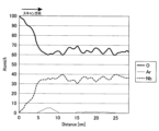
- FIG. 5 shows the measurement results of the surface area of the piezoelectric material layer in FIGS. 3 and 4 by EDX.
- the horizontal axis is the distance from the surface (principal surface) of the piezoelectric material layer
- the vertical axis is the ratio of oxygen atoms, argon atoms, and niobium atoms.
- the oxygen atomic ratio decreases from 100 atomic % to approximately 60 atomic %, and at the same time, the niobium atomic ratio increases from 0 atomic % to approximately 30 atomic %. This corresponds to a process-affected layer. Since the process-affected layer is caused by destruction of the crystal structure of lithium niobate, the niobium ratio decreases as it approaches the surface, and the oxygen ratio increases. Note that the lithium atomic ratio was not measured. On the other hand, almost no argon atoms were detected within a range of about 5 nm from the main surface of the piezoelectric material layer.
- an argon atom-containing layer with a thickness of 5 nm is formed.
- the argon atom content in the argon atom-containing layer is 2 to 6 atom %, and contains 4 atom % of argon atoms on average.
- both the oxygen atomic ratio and the niobium atomic ratio are stable, forming an unaltered portion.
- FIG. 6 A transmission electron micrograph of the surface region of the piezoelectric material substrate is shown in FIG. 6, and an explanatory diagram of FIG. 6 is shown in FIG. In FIG. 7, the upper bright region is the protective film 10, and the unaltered portion 5 of the piezoelectric material layer is present at the bottom. Argon atom-containing layer 3 is present on unaltered portion 5 .
- the process-affected layer has been removed.
- the EDS results of this surface area are approximately as shown in FIG. That is, since the process-affected layer of the piezoelectric material substrate is removed by polishing to a thickness of about 5 nm, the argon atom-containing layer is exposed on the main surface of the piezoelectric material layer. Therefore, as described above, argon atoms are contained in a range of about 5 nm from the main surface of the piezoelectric material layer, and there is an unaltered portion below.
- a measurement electrode pattern was formed on the surface of the argon atom-containing layer of the piezoelectric material layer to obtain a surface acoustic wave device.
- a SAW (surface acoustic wave) resonator was formed on the surface of the wafer by photolithography. That is, 50 reflectors were provided on each side of a comb-shaped electrode consisting of 100 pairs of electrode fingers. The electrode period was 5.66 ⁇ m for both the comb-teeth electrode and the reflector.
- the frequency characteristic S11 was measured using a network analyzer "E5072A" manufactured by Keysight. The measurement results are shown in FIG.
- the resonance frequency f r and its half-width ⁇ f r are calculated from the frequency characteristics thus obtained, and the Q value is obtained by finding f r / ⁇ f r .
- the Q value (Bode-Q) was calculated from the S11 parameter thus obtained, a maximum value of 2800 was obtained.
- Example 2 In the same manner as in Example 1, a joined body of a piezoelectric material layer in which the argon atom-containing layer was exposed on the second main surface side and a support substrate was obtained.
- the argon ion acceleration condition during argon ion trimming was set to an output of 60 W.
- EDX analysis of the surface region of the piezoelectric material layer revealed that an argon atom-containing layer was formed within a range of 4 nm from the main surface. Further, the maximum value of the argon atomic ratio was 3 atomic %, and the average was 2 atomic %.
- a surface acoustic wave device was fabricated using this bonded body in the same manner as in Example 1, and the Q value was measured, and was found to be 2400 at maximum.
- Comparative example 1 In the same manner as in Example 1, a joined body of the piezoelectric material layer and the support substrate was obtained. However, in Comparative Example 1, unlike Example 1, argon ion trimming of the main surface of the piezoelectric material layer was not performed. Therefore, lithium niobate was exposed on the main surface of the piezoelectric material layer, and no process-affected layer or argon atom-containing layer was formed. A surface acoustic wave device was fabricated using this bonded body in the same manner as in Example 1, and the Q value was measured, and the maximum was 1800.
- Comparative example 2 In the same manner as in Example 1, a joined body of the piezoelectric material layer and the support substrate was obtained.
- Comparative Example 2 argon ion trimming of the main surface of the piezoelectric material layer was performed under the same conditions as in Example 1. However, no polishing was performed after ion trimming. Therefore, a process-affected layer containing no argon atoms was formed on the main surface of the piezoelectric material layer. A surface acoustic wave device was produced using this bonded body in the same manner as in Example 1, and the Q value was measured, and the maximum was 1150.
Landscapes
- Physics & Mathematics (AREA)
- Acoustics & Sound (AREA)
- Engineering & Computer Science (AREA)
- Chemical & Material Sciences (AREA)
- Materials Engineering (AREA)
- Manufacturing & Machinery (AREA)
- Surface Acoustic Wave Elements And Circuit Networks Thereof (AREA)
Priority Applications (6)
| Application Number | Priority Date | Filing Date | Title |
|---|---|---|---|
| KR1020247035752A KR102937541B1 (ko) | 2022-03-30 | 2022-11-10 | 접합체 및 탄성파 소자 |
| JP2024511194A JP7682379B2 (ja) | 2022-03-30 | 2022-11-10 | 接合体および弾性波素子 |
| DE112022006665.2T DE112022006665T5 (de) | 2022-03-30 | 2022-11-10 | Gelenkkörper und elastisches Wellenelement |
| CN202280093066.2A CN118872204A (zh) | 2022-03-30 | 2022-11-10 | 接合体及弹性波元件 |
| US18/899,612 US20250023551A1 (en) | 2022-03-30 | 2024-09-27 | Joint body and elastic wave element |
| JP2025080369A JP7811679B2 (ja) | 2022-03-30 | 2025-05-13 | 接合体および弾性波素子 |
Applications Claiming Priority (2)
| Application Number | Priority Date | Filing Date | Title |
|---|---|---|---|
| JP2022-056518 | 2022-03-30 | ||
| JP2022056518 | 2022-03-30 |
Related Child Applications (1)
| Application Number | Title | Priority Date | Filing Date |
|---|---|---|---|
| US18/899,612 Continuation US20250023551A1 (en) | 2022-03-30 | 2024-09-27 | Joint body and elastic wave element |
Publications (1)
| Publication Number | Publication Date |
|---|---|
| WO2023188514A1 true WO2023188514A1 (ja) | 2023-10-05 |
Family
ID=88199939
Family Applications (1)
| Application Number | Title | Priority Date | Filing Date |
|---|---|---|---|
| PCT/JP2022/041912 Ceased WO2023188514A1 (ja) | 2022-03-30 | 2022-11-10 | 接合体および弾性波素子 |
Country Status (6)
| Country | Link |
|---|---|
| US (1) | US20250023551A1 (https=) |
| JP (2) | JP7682379B2 (https=) |
| KR (1) | KR102937541B1 (https=) |
| CN (1) | CN118872204A (https=) |
| DE (1) | DE112022006665T5 (https=) |
| WO (1) | WO2023188514A1 (https=) |
Cited By (1)
| Publication number | Priority date | Publication date | Assignee | Title |
|---|---|---|---|---|
| WO2026039074A1 (en) * | 2024-08-16 | 2026-02-19 | Tel Manufacturing And Engineering Of America, Inc. | Method for processing a substrate |
Citations (5)
| Publication number | Priority date | Publication date | Assignee | Title |
|---|---|---|---|---|
| JPH06303073A (ja) * | 1993-02-17 | 1994-10-28 | Fujitsu Ltd | 弾性表面波デバイスとその製造方法 |
| JPH07202631A (ja) * | 1993-11-25 | 1995-08-04 | Fujitsu Ltd | 弾性表面波装置及びその製造方法 |
| JP2011171359A (ja) * | 2010-02-16 | 2011-09-01 | Hitachi Cable Ltd | 圧電薄膜素子及び圧電薄膜デバイス |
| US20180175826A1 (en) * | 2016-12-15 | 2018-06-21 | Qorvo Us, Inc. | Bulk acoustic wave resonator with multilayer piezoelectric structure |
| JP2020182137A (ja) * | 2019-04-26 | 2020-11-05 | 京セラ株式会社 | 弾性波装置 |
Family Cites Families (1)
| Publication number | Priority date | Publication date | Assignee | Title |
|---|---|---|---|---|
| WO2020250490A1 (ja) | 2019-06-11 | 2020-12-17 | 日本碍子株式会社 | 複合基板、弾性波素子および複合基板の製造方法 |
-
2022
- 2022-11-10 DE DE112022006665.2T patent/DE112022006665T5/de active Pending
- 2022-11-10 WO PCT/JP2022/041912 patent/WO2023188514A1/ja not_active Ceased
- 2022-11-10 CN CN202280093066.2A patent/CN118872204A/zh active Pending
- 2022-11-10 JP JP2024511194A patent/JP7682379B2/ja active Active
- 2022-11-10 KR KR1020247035752A patent/KR102937541B1/ko active Active
-
2024
- 2024-09-27 US US18/899,612 patent/US20250023551A1/en active Pending
-
2025
- 2025-05-13 JP JP2025080369A patent/JP7811679B2/ja active Active
Patent Citations (5)
| Publication number | Priority date | Publication date | Assignee | Title |
|---|---|---|---|---|
| JPH06303073A (ja) * | 1993-02-17 | 1994-10-28 | Fujitsu Ltd | 弾性表面波デバイスとその製造方法 |
| JPH07202631A (ja) * | 1993-11-25 | 1995-08-04 | Fujitsu Ltd | 弾性表面波装置及びその製造方法 |
| JP2011171359A (ja) * | 2010-02-16 | 2011-09-01 | Hitachi Cable Ltd | 圧電薄膜素子及び圧電薄膜デバイス |
| US20180175826A1 (en) * | 2016-12-15 | 2018-06-21 | Qorvo Us, Inc. | Bulk acoustic wave resonator with multilayer piezoelectric structure |
| JP2020182137A (ja) * | 2019-04-26 | 2020-11-05 | 京セラ株式会社 | 弾性波装置 |
Cited By (1)
| Publication number | Priority date | Publication date | Assignee | Title |
|---|---|---|---|---|
| WO2026039074A1 (en) * | 2024-08-16 | 2026-02-19 | Tel Manufacturing And Engineering Of America, Inc. | Method for processing a substrate |
Also Published As
| Publication number | Publication date |
|---|---|
| CN118872204A (zh) | 2024-10-29 |
| DE112022006665T5 (de) | 2024-12-12 |
| KR20240167884A (ko) | 2024-11-28 |
| KR102937541B1 (ko) | 2026-03-10 |
| JP7811679B2 (ja) | 2026-02-05 |
| JPWO2023188514A1 (https=) | 2023-10-05 |
| JP7682379B2 (ja) | 2025-05-23 |
| US20250023551A1 (en) | 2025-01-16 |
| JP2025107428A (ja) | 2025-07-17 |
Similar Documents
| Publication | Publication Date | Title |
|---|---|---|
| JP6375471B1 (ja) | 接合体および弾性波素子 | |
| KR102428548B1 (ko) | 접합 방법 | |
| KR102123350B1 (ko) | 탄성파 소자 및 그 제조 방법 | |
| KR102222096B1 (ko) | 탄성파 소자 및 그 제조 방법 | |
| WO2017163723A1 (ja) | 接合方法 | |
| JPWO2020079958A1 (ja) | 接合体および弾性波素子 | |
| JP6850401B1 (ja) | 接合体および弾性波素子 | |
| WO2018096797A1 (ja) | 接合体 | |
| JP7811679B2 (ja) | 接合体および弾性波素子 | |
| JP6605184B1 (ja) | 接合体および弾性波素子 | |
| JP6393015B1 (ja) | 弾性波素子およびその製造方法 | |
| JP6612002B1 (ja) | 接合体および弾性波素子 | |
| EP4068624B1 (en) | Bonded body comprising piezoelectric material substrate and support substrate | |
| JPWO2021002046A1 (ja) | 接合体および弾性波素子 | |
| WO2022054372A1 (ja) | 弾性波デバイス用複合基板 | |
| CN114731150B (zh) | 压电性材料基板与支撑基板的接合体 | |
| TWI743700B (zh) | 4g頻帶用彈性表面波元件 | |
| KR20250160194A (ko) | 접합체의 제조 방법 |
Legal Events
| Date | Code | Title | Description |
|---|---|---|---|
| 121 | Ep: the epo has been informed by wipo that ep was designated in this application |
Ref document number: 22935643 Country of ref document: EP Kind code of ref document: A1 |
|
| ENP | Entry into the national phase |
Ref document number: 2024511194 Country of ref document: JP Kind code of ref document: A |
|
| WWE | Wipo information: entry into national phase |
Ref document number: 202280093066.2 Country of ref document: CN |
|
| WWE | Wipo information: entry into national phase |
Ref document number: 112022006665 Country of ref document: DE |
|
| ENP | Entry into the national phase |
Ref document number: 20247035752 Country of ref document: KR Kind code of ref document: A |
|
| WWE | Wipo information: entry into national phase |
Ref document number: 1020247035752 Country of ref document: KR |
|
| 122 | Ep: pct application non-entry in european phase |
Ref document number: 22935643 Country of ref document: EP Kind code of ref document: A1 |