WO2023188080A1 - タッチセンサ、表示装置 - Google Patents
タッチセンサ、表示装置 Download PDFInfo
- Publication number
- WO2023188080A1 WO2023188080A1 PCT/JP2022/015877 JP2022015877W WO2023188080A1 WO 2023188080 A1 WO2023188080 A1 WO 2023188080A1 JP 2022015877 W JP2022015877 W JP 2022015877W WO 2023188080 A1 WO2023188080 A1 WO 2023188080A1
- Authority
- WO
- WIPO (PCT)
- Prior art keywords
- touch sensor
- conductor
- sensor according
- wiring
- mesh
- Prior art date
- Legal status (The legal status is an assumption and is not a legal conclusion. Google has not performed a legal analysis and makes no representation as to the accuracy of the status listed.)
- Ceased
Links
Images


Classifications
-
- G—PHYSICS
- G06—COMPUTING OR CALCULATING; COUNTING
- G06F—ELECTRIC DIGITAL DATA PROCESSING
- G06F3/00—Input arrangements for transferring data to be processed into a form capable of being handled by the computer; Output arrangements for transferring data from processing unit to output unit, e.g. interface arrangements
- G06F3/01—Input arrangements or combined input and output arrangements for interaction between user and computer
- G06F3/03—Arrangements for converting the position or the displacement of a member into a coded form
- G06F3/041—Digitisers, e.g. for touch screens or touch pads, characterised by the transducing means
- G06F3/044—Digitisers, e.g. for touch screens or touch pads, characterised by the transducing means by capacitive means
- G06F3/0446—Digitisers, e.g. for touch screens or touch pads, characterised by the transducing means by capacitive means using a grid-like structure of electrodes in at least two directions, e.g. using row and column electrodes
-
- G—PHYSICS
- G06—COMPUTING OR CALCULATING; COUNTING
- G06F—ELECTRIC DIGITAL DATA PROCESSING
- G06F3/00—Input arrangements for transferring data to be processed into a form capable of being handled by the computer; Output arrangements for transferring data from processing unit to output unit, e.g. interface arrangements
- G06F3/01—Input arrangements or combined input and output arrangements for interaction between user and computer
- G06F3/03—Arrangements for converting the position or the displacement of a member into a coded form
- G06F3/041—Digitisers, e.g. for touch screens or touch pads, characterised by the transducing means
- G06F3/0412—Digitisers structurally integrated in a display
-
- G—PHYSICS
- G06—COMPUTING OR CALCULATING; COUNTING
- G06F—ELECTRIC DIGITAL DATA PROCESSING
- G06F3/00—Input arrangements for transferring data to be processed into a form capable of being handled by the computer; Output arrangements for transferring data from processing unit to output unit, e.g. interface arrangements
- G06F3/01—Input arrangements or combined input and output arrangements for interaction between user and computer
- G06F3/03—Arrangements for converting the position or the displacement of a member into a coded form
- G06F3/041—Digitisers, e.g. for touch screens or touch pads, characterised by the transducing means
- G06F3/044—Digitisers, e.g. for touch screens or touch pads, characterised by the transducing means by capacitive means
- G06F3/0448—Details of the electrode shape, e.g. for enhancing the detection of touches, for generating specific electric field shapes, for enhancing display quality
-
- G—PHYSICS
- G06—COMPUTING OR CALCULATING; COUNTING
- G06F—ELECTRIC DIGITAL DATA PROCESSING
- G06F2203/00—Indexing scheme relating to G06F3/00 - G06F3/048
- G06F2203/041—Indexing scheme relating to G06F3/041 - G06F3/045
- G06F2203/04112—Electrode mesh in capacitive digitiser: electrode for touch sensing is formed of a mesh of very fine, normally metallic, interconnected lines that are almost invisible to see. This provides a quite large but transparent electrode surface, without need for ITO or similar transparent conductive material
Definitions
- the present invention relates to a touch sensor and a display device.
- Patent Document 1 discloses a structure of a touch sensor using a metal mesh.
- display unevenness caused by the touch sensor may be visually recognized.
- a touch sensor includes a first conductor having a mesh wiring, and a second conductor adjacent to the first conductor and having a mesh wiring, the first conductor and the second conductor having a mesh wiring. At least a portion of the boundary portion extends in the first direction, and the mesh wiring of the first conductor includes a plurality of disconnection points formed such that disconnection edges intersect the first direction in a plan view.
- display unevenness caused by a touch sensor is reduced when applied to a display panel.
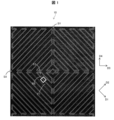
- FIG. 1 is a plan view showing the configuration of a touch sensor according to a first embodiment
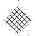
- FIG. FIG. 2 is a plan view showing an enlarged configuration of a region surrounded by white lines in FIG. 1
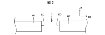
- FIG. 3 is a plan view showing the configuration of the disconnection location in FIG. 2
- FIG. 2 is a schematic diagram showing the configuration of a touch sensor.
- FIG. 2 is a schematic cross-sectional view showing the operating principle of a touch sensor.
- FIG. 3 is a cross-sectional view showing the configuration of a touch sensor.
- FIG. 3 is a cross-sectional view showing the configuration of a touch sensor.
- FIG. 2 is a plan view showing the configuration of a touch sensor.
- FIG. 1 is a schematic cross-sectional view showing the configuration of a display device according to an embodiment.
- FIG. 1 is a plan view showing the configuration of a display device according to the present embodiment.
- FIG. 1 is a plan view showing the configuration of a touch sensor according to the first embodiment.
- FIG. 2 is an enlarged plan view showing the configuration of the area surrounded by white lines in FIG. 1.
- FIG. FIG. 3 is a plan view showing the configuration of the disconnection location in FIG. 2.
- the touch sensor 10 includes a first conductor F1 having a mesh wiring (for example, metal mesh) W1, and a second conductor adjacent to the first conductor F1 having a mesh wiring W2. At least a part of the boundary BS between the first conductor F1 and the second conductor F2 extends in the first direction D1, and the mesh wiring W1 of the first conductor F1 has a disconnection edge ED in a plan view.
- a mesh wiring for example, metal mesh
- the second direction D2 is a direction orthogonal to the first direction D1.
- Planar viewing is, for example, based on a line of sight parallel to the thickness direction of the touch sensor 10, and includes perspective viewing.
- the second conductor F2 is electrically insulated from the first conductor F1, and the mesh wiring W2 of the second conductor F2 has a plurality of wires formed such that the disconnection edge ED intersects the first direction D1 in a plan view. Including the disconnection point K.
- the disconnection edge ED may be formed to be substantially perpendicular to the first direction D1, and the mesh wirings W1 and W2 have light reflective properties.
- the disconnection edge ED includes a plurality of disconnection points K formed to intersect with the first direction D1 in a plan view, so no disconnection point K is provided.
- the reflectance of light incident on the first and second conductors F1 and F2 in the second direction D2 can be suppressed. Thereby, the directivity of light reflectance is reduced, and the display quality (for example, display unevenness) of the display panel including the touch sensor 10 can be improved.
- FIG. 4 is a schematic diagram showing the configuration of the touch sensor.
- the touch sensor 10 has a plurality of first sensing lines SX extending in a third direction D3 (for example, horizontal direction) that forms an angle of +45 degrees or -45 degrees with the first direction D1, and a fourth direction D4 that is orthogonal to the third direction D3. (for example, in the vertical direction), the first conductor F1 is included in one of the plurality of first sensing lines SX, and the second conductor F2 is included in one of the plurality of first sensing lines SX. may be included in one of the second sensing lines SY.
- FIG. 5 is a schematic cross-sectional view showing the operating principle of the touch sensor.
- a sensing target UB such as a finger
- the capacitance of a specific first sensing line SX and a specific second sensing line SY changes, and the sensing current read from them changes.
- the position of the sensing target UB is specified.
- each mesh of the mesh wiring W1 and W2 may be a rectangle (for example, a square) having sides parallel to the first direction D1 and sides parallel to the second direction D2.
- two disconnection points K1 and K2 arranged in a second direction D2 orthogonal to the first direction D1 may be provided in an annular portion surrounding the mesh AM.
- the outer shape of each of the first conductor F1 and the second conductor F2 may be V-shaped.
- the plurality of lattice cut portions LS are arranged in a staggered shape when viewed in the second direction D2. It may be located in The width of the boundary portion BS (size in the second direction D2) may be twice or less the mesh diameter of the first conductor F1.
- a configuration may be adopted in which no disconnection location is formed in the portion extending in the second direction D2.
- FIG. 6 and 7 are cross-sectional views showing the configuration of the touch sensor.
- FIG. 8 is a plan view showing the configuration of the touch sensor.
- the fifth direction D5 is the thickness direction of the mesh wiring.
- the base coat film 7, the interlayer insulating film 8, and the mesh wiring W1 and W2 may be formed in this order.
- An overcoat film (not shown) may be formed to cover the mesh wirings W1 and W2.
- Each of the mesh wirings W1 and W1 may be composed of a laminate of metal films. This laminate may include a titanium film and an aluminum film.
- each of the mesh wiring W1 of the first conductor F1 and the mesh wiring W2 of the second conductor F2 has a plurality of boundary edges EK facing the boundary portion BS.
- N/M may be set to 0.75 to 1.25. can.
- the reflectance of light incident on the first and second conductors F1 and F2 in the first direction D1 and the reflectance of light incident on the first and second conductors F1 and F2 in the second direction D2 can be adjusted.
- the reflectance of light can be made even, and uneven reflection can be effectively suppressed.
- the difference between the reflectance of light in the D1 direction and the reflectance of light in the D2 direction can be, for example, less than 10% (preferably less than 5%).
- a plurality of island-shaped conductors SD may be arranged within the boundary portion BS.
- the island-shaped conductor SD may have an inverted tapered shape in which the length of the upper surface is smaller than the length of the lower surface.
- the disconnection point K may have the shape of a wiring notch, and the notch length KL may be equal to or greater than the wiring width HW.
- the notch length KL may be greater than the wiring thickness.
- FIG. 9 is a schematic cross-sectional view showing the configuration of the display device according to this embodiment.
- the display device 20 includes a substrate 1, a pixel circuit layer 2, a light emitting element layer 3, a sealing layer 4, and a touch sensor 10 in this order.
- the substrate 1, the pixel circuit layer 2, the light emitting element layer 3, and the sealing layer 4 may constitute the OLED panel 9.
- the touch sensor 10 may be monolithically formed on the OLED panel 9 (so-called on-cell structure).
- the substrate 1 may be flexible.
- FIG. 10 is a plan view showing the configuration of the display device according to this embodiment.
- the light emitting regions 3E of each light emitting element for example, an organic light emitting diode or a quantum dot light emitting diode
- the touch sensor 10 of this embodiment has high sensitivity, the vertical scanning period for driving the OLED panel 9 and the sensing period of the touch sensor 10 can be overlapped (temporally).
Landscapes
- Engineering & Computer Science (AREA)
- General Engineering & Computer Science (AREA)
- Theoretical Computer Science (AREA)
- Human Computer Interaction (AREA)
- Physics & Mathematics (AREA)
- General Physics & Mathematics (AREA)
- Quality & Reliability (AREA)
- Position Input By Displaying (AREA)
- Devices For Indicating Variable Information By Combining Individual Elements (AREA)
Priority Applications (3)
| Application Number | Priority Date | Filing Date | Title |
|---|---|---|---|
| PCT/JP2022/015877 WO2023188080A1 (ja) | 2022-03-30 | 2022-03-30 | タッチセンサ、表示装置 |
| US18/833,942 US20250117101A1 (en) | 2022-03-30 | 2022-03-30 | Touch sensor and display device |
| JP2024510865A JP7723833B2 (ja) | 2022-03-30 | 2022-03-30 | タッチセンサ、表示装置 |
Applications Claiming Priority (1)
| Application Number | Priority Date | Filing Date | Title |
|---|---|---|---|
| PCT/JP2022/015877 WO2023188080A1 (ja) | 2022-03-30 | 2022-03-30 | タッチセンサ、表示装置 |
Publications (1)
| Publication Number | Publication Date |
|---|---|
| WO2023188080A1 true WO2023188080A1 (ja) | 2023-10-05 |
Family
ID=88200179
Family Applications (1)
| Application Number | Title | Priority Date | Filing Date |
|---|---|---|---|
| PCT/JP2022/015877 Ceased WO2023188080A1 (ja) | 2022-03-30 | 2022-03-30 | タッチセンサ、表示装置 |
Country Status (3)
| Country | Link |
|---|---|
| US (1) | US20250117101A1 (https=) |
| JP (1) | JP7723833B2 (https=) |
| WO (1) | WO2023188080A1 (https=) |
Families Citing this family (1)
| Publication number | Priority date | Publication date | Assignee | Title |
|---|---|---|---|---|
| CN115686254A (zh) * | 2022-06-06 | 2023-02-03 | 武汉华星光电半导体显示技术有限公司 | 触控显示面板 |
Citations (5)
| Publication number | Priority date | Publication date | Assignee | Title |
|---|---|---|---|---|
| WO2015156316A1 (ja) * | 2014-04-08 | 2015-10-15 | 株式会社フジクラ | 配線体及び配線基板 |
| JP2016099693A (ja) * | 2014-11-19 | 2016-05-30 | 株式会社ジャパンディスプレイ | 表示装置 |
| JP2017102811A (ja) * | 2015-12-04 | 2017-06-08 | 株式会社ジャパンディスプレイ | 表示装置および入力装置 |
| US20190189699A1 (en) * | 2017-12-14 | 2019-06-20 | Wuhan China Star Optoelectronics Semiconductor Display Technology Co., Ltd. | Flexible touch panel and oled display panel |
| US20190250738A1 (en) * | 2018-02-13 | 2019-08-15 | Samsung Display Co., Ltd. | Display device including mesh lines overlapping contact holes |
-
2022
- 2022-03-30 WO PCT/JP2022/015877 patent/WO2023188080A1/ja not_active Ceased
- 2022-03-30 US US18/833,942 patent/US20250117101A1/en active Pending
- 2022-03-30 JP JP2024510865A patent/JP7723833B2/ja active Active
Patent Citations (5)
| Publication number | Priority date | Publication date | Assignee | Title |
|---|---|---|---|---|
| WO2015156316A1 (ja) * | 2014-04-08 | 2015-10-15 | 株式会社フジクラ | 配線体及び配線基板 |
| JP2016099693A (ja) * | 2014-11-19 | 2016-05-30 | 株式会社ジャパンディスプレイ | 表示装置 |
| JP2017102811A (ja) * | 2015-12-04 | 2017-06-08 | 株式会社ジャパンディスプレイ | 表示装置および入力装置 |
| US20190189699A1 (en) * | 2017-12-14 | 2019-06-20 | Wuhan China Star Optoelectronics Semiconductor Display Technology Co., Ltd. | Flexible touch panel and oled display panel |
| US20190250738A1 (en) * | 2018-02-13 | 2019-08-15 | Samsung Display Co., Ltd. | Display device including mesh lines overlapping contact holes |
Also Published As
| Publication number | Publication date |
|---|---|
| US20250117101A1 (en) | 2025-04-10 |
| JP7723833B2 (ja) | 2025-08-14 |
| JPWO2023188080A1 (https=) | 2023-10-05 |
Similar Documents
| Publication | Publication Date | Title |
|---|---|---|
| KR102736214B1 (ko) | 전자 장치 | |
| TWI796372B (zh) | 導電構件及觸控面板 | |
| CN108695369B (zh) | 具有微盖层的显示装置及其制造方法 | |
| US12242698B2 (en) | Touchscreen | |
| CN115210677A (zh) | 显示面板和显示装置 | |
| KR20170046683A (ko) | 보강된 부분을 갖는 배선을 포함하는 플렉서블 디스플레이 디바이스 및 이의 제조 방법 | |
| US20190235668A1 (en) | Touch screen and mobile terminal | |
| CN112119444B (zh) | 显示面板和显示装置 | |
| KR20170064139A (ko) | 터치 패널 | |
| TWI787293B (zh) | 觸控面板及顯示裝置 | |
| WO2023188080A1 (ja) | タッチセンサ、表示装置 | |
| CN205486028U (zh) | 一种触控显示面板和触控显示装置 | |
| JP2019533840A (ja) | タッチ構造及びその製造方法並びにタッチ装置 | |
| JPWO2023188080A5 (https=) | ||
| JP6205995B2 (ja) | タッチパネルセンサおよびタッチ位置検出機能付き表示装置 | |
| TW201941039A (zh) | 觸控面板及顯示裝置 | |
| JP6615975B2 (ja) | タッチパネル | |
| JP6433566B2 (ja) | 表示装置 | |
| JP6074533B2 (ja) | 表示装置 | |
| JP6231705B2 (ja) | タッチパネル | |
| KR20250019230A (ko) | 입력 센서 및 이를 포함하는 표시 장치 | |
| TWM518823U (zh) | 顯示面板 | |
| JP2015204066A (ja) | タッチパネルセンサ、及び、タッチ位置検出機能付き表示装置 |
Legal Events
| Date | Code | Title | Description |
|---|---|---|---|
| 121 | Ep: the epo has been informed by wipo that ep was designated in this application |
Ref document number: 22935226 Country of ref document: EP Kind code of ref document: A1 |
|
| ENP | Entry into the national phase |
Ref document number: 2024510865 Country of ref document: JP Kind code of ref document: A |
|
| WWE | Wipo information: entry into national phase |
Ref document number: 18833942 Country of ref document: US |
|
| NENP | Non-entry into the national phase |
Ref country code: DE |
|
| 122 | Ep: pct application non-entry in european phase |
Ref document number: 22935226 Country of ref document: EP Kind code of ref document: A1 |
|
| WWP | Wipo information: published in national office |
Ref document number: 18833942 Country of ref document: US |