WO2023181944A1 - 冷却器および半導体モジュール - Google Patents
冷却器および半導体モジュール Download PDFInfo
- Publication number
- WO2023181944A1 WO2023181944A1 PCT/JP2023/008826 JP2023008826W WO2023181944A1 WO 2023181944 A1 WO2023181944 A1 WO 2023181944A1 JP 2023008826 W JP2023008826 W JP 2023008826W WO 2023181944 A1 WO2023181944 A1 WO 2023181944A1
- Authority
- WO
- WIPO (PCT)
- Prior art keywords
- cooler
- main surface
- heat dissipation
- recess
- cooler according
- Prior art date
- Legal status (The legal status is an assumption and is not a legal conclusion. Google has not performed a legal analysis and makes no representation as to the accuracy of the status listed.)
- Ceased
Links
Images







Classifications
-
- H—ELECTRICITY
- H10—SEMICONDUCTOR DEVICES; ELECTRIC SOLID-STATE DEVICES NOT OTHERWISE PROVIDED FOR
- H10W—GENERIC PACKAGES, INTERCONNECTIONS, CONNECTORS OR OTHER CONSTRUCTIONAL DETAILS OF DEVICES COVERED BY CLASS H10
- H10W40/00—Arrangements for thermal protection or thermal control
- H10W40/20—Arrangements for cooling
- H10W40/22—Arrangements for cooling characterised by their shape, e.g. having conical or cylindrical projections
-
- H—ELECTRICITY
- H10—SEMICONDUCTOR DEVICES; ELECTRIC SOLID-STATE DEVICES NOT OTHERWISE PROVIDED FOR
- H10W—GENERIC PACKAGES, INTERCONNECTIONS, CONNECTORS OR OTHER CONSTRUCTIONAL DETAILS OF DEVICES COVERED BY CLASS H10
- H10W40/00—Arrangements for thermal protection or thermal control
- H10W40/10—Arrangements for heating
-
- H—ELECTRICITY
- H10—SEMICONDUCTOR DEVICES; ELECTRIC SOLID-STATE DEVICES NOT OTHERWISE PROVIDED FOR
- H10W—GENERIC PACKAGES, INTERCONNECTIONS, CONNECTORS OR OTHER CONSTRUCTIONAL DETAILS OF DEVICES COVERED BY CLASS H10
- H10W40/00—Arrangements for thermal protection or thermal control
- H10W40/20—Arrangements for cooling
- H10W40/25—Arrangements for cooling characterised by their materials
- H10W40/255—Arrangements for cooling characterised by their materials having a laminate or multilayered structure, e.g. direct bond copper [DBC] ceramic substrates
-
- H—ELECTRICITY
- H10—SEMICONDUCTOR DEVICES; ELECTRIC SOLID-STATE DEVICES NOT OTHERWISE PROVIDED FOR
- H10W—GENERIC PACKAGES, INTERCONNECTIONS, CONNECTORS OR OTHER CONSTRUCTIONAL DETAILS OF DEVICES COVERED BY CLASS H10
- H10W40/00—Arrangements for thermal protection or thermal control
- H10W40/40—Arrangements for thermal protection or thermal control involving heat exchange by flowing fluids
- H10W40/47—Arrangements for thermal protection or thermal control involving heat exchange by flowing fluids by flowing liquids, e.g. forced water cooling
-
- H—ELECTRICITY
- H10—SEMICONDUCTOR DEVICES; ELECTRIC SOLID-STATE DEVICES NOT OTHERWISE PROVIDED FOR
- H10W—GENERIC PACKAGES, INTERCONNECTIONS, CONNECTORS OR OTHER CONSTRUCTIONAL DETAILS OF DEVICES COVERED BY CLASS H10
- H10W40/00—Arrangements for thermal protection or thermal control
- H10W40/60—Securing means for detachable heating or cooling arrangements, e.g. clamps
- H10W40/611—Bolts or screws
-
- H—ELECTRICITY
- H10—SEMICONDUCTOR DEVICES; ELECTRIC SOLID-STATE DEVICES NOT OTHERWISE PROVIDED FOR
- H10W—GENERIC PACKAGES, INTERCONNECTIONS, CONNECTORS OR OTHER CONSTRUCTIONAL DETAILS OF DEVICES COVERED BY CLASS H10
- H10W40/00—Arrangements for thermal protection or thermal control
- H10W40/20—Arrangements for cooling
- H10W40/231—Arrangements for cooling characterised by their places of attachment or cooling paths
- H10W40/235—Arrangements for cooling characterised by their places of attachment or cooling paths attached to package parts
Definitions
- the present disclosure relates to a cooler.
- the present disclosure also relates to a semiconductor module including a cooler and a semiconductor device placed in the cooler.
- Patent Document 1 discloses an example of a cooler in which a semiconductor device is placed.
- the cooler includes a casing having a hollow area and a radiator.
- the housing is provided with an opening leading to the hollow area.
- the radiator is attached to the housing so as to close the opening.
- the semiconductor device is bonded to a portion of the heat sink that protrudes from the hollow region. When the hollow region is filled with cooling water, the cooling water contacts the radiator. Thereby, the semiconductor device can be cooled.
- the semiconductor device is cooled indirectly via the heat radiator. Furthermore, since a gap is provided between the radiator and the housing in the hollow region, cooling water tends to flow concentrated in the gap. As a result, the cooling water may not be able to sufficiently cool the radiator and the semiconductor device.
- An object of the present disclosure is to provide a cooler that is improved over conventional coolers, and by extension, a semiconductor module that includes the cooler.
- an object of the present disclosure is to provide a cooler and a semiconductor module that can improve cooling efficiency with a simpler structure.
- a cooler provided by a first aspect of the present disclosure includes: a recess that opens on one side in a first direction; a bottom that is located on the other side in the first direction and defines a part of the recess; and a heat dissipation member attached to the bottom and at least partially housed in the recess.
- the bottom portion includes a flexible portion that is elastically deformed. When a load directed toward the other side in the first direction is applied to the heat radiating member, an elastic force generated from the flexible portion and directed toward the one side in the first direction acts on the heat radiating member.
- a semiconductor module provided by a second aspect of the present disclosure includes a cooler provided by the first aspect of the present disclosure, a semiconductor device placed in the cooler, and a semiconductor device held in the cooler. and a mounting member.
- the semiconductor device covers the recess, and the heat radiation member is in contact with the semiconductor device.
- a load directed toward the side where the heat dissipation member is located in the first direction is applied from the mounting member to the semiconductor device.
- FIG. 1 is a plan view of a cooler according to a first embodiment of the present disclosure.
- FIG. 2 is a front view of the cooler shown in FIG. 1.
- 3 is a left side view of the cooler shown in FIG. 1.
- FIG. FIG. 4 is a partially enlarged view of FIG.
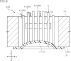
- FIG. 5 is a sectional view taken along line VV in FIG. 4.
- FIG. 6 is a sectional view taken along line VI-VI in FIG. 4.
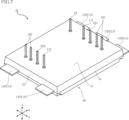
- FIG. 7 is a perspective view of one of a plurality of semiconductor devices that constitute the semiconductor module shown in FIG. 20.
- FIG. 8 is a plan view of the semiconductor device shown in FIG. 7.
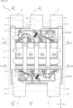
- FIG. 9 is a plan view corresponding to FIG. 8, in which the sealing resin is seen through.
- FIG. 10 is a partially enlarged view of FIG. 9.
- FIG. 9 is a plan view of FIG. 9.
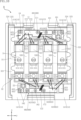
- FIG. 11 is a plan view corresponding to FIG. 8, in which the first conductive member is seen through, and the sealing resin and the second conductive member are not shown.
- 12 is a right side view of the semiconductor device shown in FIG. 7.
- FIG. 13 is a bottom view of the semiconductor device shown in FIG. 7.
- FIG. 14 is a cross-sectional view taken along line XIV-XIV in FIG. 9.
- FIG. 15 is a cross-sectional view taken along line XV-XV in FIG.
- FIG. 16 is a partially enlarged view of the first element shown in FIG. 15 and its surroundings.
- FIG. 17 is a partially enlarged view of the second element shown in FIG. 15 and its surroundings.
- FIG. 18 is a cross-sectional view taken along line XVIII-XVIII in FIG.
- FIG. 19 is a cross-sectional view taken along line XIX-XIX in FIG.
- FIG. 20 is a plan view of the semiconductor module according to the first embodiment of the present disclosure.
- FIG. 21 is a front view of the semiconductor module shown in FIG. 20.
- FIG. 22 is a partially enlarged sectional view of the semiconductor module shown in FIG. 20.
- FIG. 23 is a partially enlarged plan view of the cooler according to the second embodiment of the present disclosure.
- FIG. 24 is a cross-sectional view taken along line XXIV-XXIV in FIG. 23.
- FIG. 25 is a cross-sectional view taken along line XXV-XXV in FIG. 23.
- FIG. 26 is a partially enlarged sectional view of a semiconductor module according to a second embodiment of the present disclosure.
- FIG. 27 is a partially enlarged plan view of the cooler according to the third embodiment of the present disclosure.
- FIG. 28 is a cross-sectional view taken along line XXVIII-XXVIII in FIG. 27.
- FIG. 29 is a cross-sectional view taken along line XXIX-XXIX in FIG. 27.
- FIG. 30 is a partially enlarged sectional view of a semiconductor module according to a third embodiment of the present disclosure.
- FIG. 31 is a partially enlarged plan view of the cooler according to the fourth embodiment of the present disclosure.
- FIG. 32 is a sectional view taken along line XXXII-XXXII in FIG. 31.
- FIG. 33 is a sectional view taken along the line XXXIII-XXXIII in FIG. 31.
- FIG. 34 is a partially enlarged sectional view of a semiconductor module according to a fourth embodiment of the present disclosure.
- FIG. 35 is a partially enlarged plan view of a cooler according to a
- Cooler A10 according to a first embodiment of the present disclosure will be described based on FIGS. 1 to 6.
- the cooler A10 is used to cool a plurality of semiconductor devices B that constitute a semiconductor module C10, which will be described later.
- Cooler A10 includes a housing 70 and a heat radiation member 81.
- first direction z A direction perpendicular to the first direction z is called a "second direction x.”
- second direction x A direction perpendicular to the first direction z and the second direction x is referred to as a "third direction y.”
- the first direction z, the second direction x, and the third direction y are also applied to the description of the semiconductor device B and the semiconductor module C10, which will be described later.
- the housing 70 constitutes the main part of the cooler A10, as shown in FIGS. 1 and 2.
- the housing 70 is integrally formed except for the bottom portion 72.
- the integrally molded portion of the housing 70 is made of a material containing aluminum, for example.
- the housing 70 has a plurality of recesses 71 and a plurality of bottoms 72.
- the plurality of recesses 71 are open on one side in the first direction z.
- the plurality of recesses 71 are arranged along the third direction y.
- the plurality of bottom portions 72 are located on the other side in the first direction z, and individually define a portion of each of the plurality of recesses 71 .
- the housing 70 has a main surface 701 and a back surface 702.
- the main surface 701 faces the side where the heat dissipation member 81 is located with respect to the bottom portion 72 in the first direction z.
- Main surface 701 surrounds recess 71 .
- the recessed portion 71 is recessed from the main surface 701 in the first direction z.
- the back surface 702 faces the opposite side from the main surface 701 in the first direction z.
- Each of the plurality of bottom portions 72 includes a flexible portion 721 that is elastically deformed.
- the flexible portion 721 is integrally formed.
- the entire bottom portion 72 is a flexible portion 721.
- the flexible portion 721 is made of a material containing natural rubber, for example.
- the material of the flexible portion 721 may be metal.
- the bottom portion 72 is joined to the back surface 702 of the housing 70 by vulcanization adhesive or the like.
- the bottom portion 72 may be integrated with the housing 70.
- the configuration of the bottom portion 72 is not limited as long as it includes a flexible portion 721 that is elastically deformed.
- the heat dissipation member 81 is attached to the bottom portion 72, as shown in FIGS. 5 and 6. At least a portion of the heat dissipating member 81 is accommodated in the recess 71 .
- the thermal conductivity of the heat dissipating member 81 is higher than that of the housing 70.
- the heat dissipation member 81 includes a first member 811, a second member 812, a third member 813, a fourth member 814, and a fifth member 815 that are separated from each other.
- the first member 811 , the second member 812 , the third member 813 , the fourth member 814 , and the fifth member 815 are rod-shaped and extend in the first direction z, and are supported by the flexible portion 721 of the bottom portion 72 .
- the first member 811, the second member 812, the third member 813, the fourth member 814, and the fifth member 815 have the same dimensions in the first direction z. As shown in FIG.
- the first member 811, the second member 812, the third member 813, the fourth member 814, and the fifth member 815 are surrounded by the main surface 701 of the housing 70. It is. As shown in FIGS. 5 and 6, when the flexible portion 721 is in its natural state, a portion of each of the first member 811, the second member 812, the third member 813, the fourth member 814, and the fifth member 815 includes a portion protruding outward from main surface 701.
- the natural state of the flexible portion 721 refers to a state where only the weight of the heat dissipation member 81 is acting on it.
- the first member 811 and the second member 812 are separated from each other in the second direction x.
- the first member 811 is located closest to the center C of the recess 71 when viewed in the first direction z. When viewed in the first direction z, the center C coincides with the center of gravity of the planar figure formed by the periphery of the recess 71 .
- the second member 812 is located closest to the main surface 701 of the housing 70 .
- the third member 813 is located between the first member 811 and the second member 812 in the second direction x.
- the amount of protrusion L1 of the first member 811 from the main surface 701 of the casing 70 to the outside is equal to This is larger than the protrusion amount L2 of the second member 812.
- a protrusion amount L3 of the third member 813 from the main surface 701 to the outside is smaller than the protrusion amount L1 and larger than the protrusion amount L2.
- the first member 811 and the fourth member 814 are separated from each other in the third direction y.
- the fourth member 814 is located closest to the main surface 701 of the housing 70 .
- the fifth member 815 is located between the first member 811 and the fourth member 814 in the third direction y.
- the amount of protrusion L1 of the first member 811 from the main surface 701 of the casing 70 to the outside is equal to This is larger than the protrusion amount L4 of the fourth member 814. Additionally, the amount of protrusion L5 of the fifth member 815 from the main surface 701 to the outside is smaller than the amount of protrusion L1 and larger than the amount of protrusion L4.
- the bottom portion 72 bulges toward the side where the heat dissipation member 81 is located in the first direction z.
- the center C shown in FIG. 4 is located farthest from the back surface 702 of the housing 70 in the first direction z.
- each of the plurality of recesses 71 is provided with an inlet 711 and an outlet 712.
- the inlet 711 and the outlet 712 are located on opposite sides of the recess 71 in the third direction y.
- the inlet 711 and the outlet 712 are located between the main surface 701 and the back surface 702 of the housing 70 in the first direction z.
- the inlet 711 and the outlet 712 are connected to the recess 71 .
- the first member 811 of the heat radiating member 81 overlaps the inlet 711 and the outlet 712 when viewed in the third direction y.
- the distance d1 between the inlet 711 and the main surface 701 of the casing 70 in the first direction z is larger than the distance d2 between the inlet 711 and the back surface 702 of the casing 70 in the first direction z. short.
- the distance d3 between the outlet 712 and the main surface 701 in the first direction z is shorter than the distance d4 between the outlet 712 and the back surface 702 in the first direction z.
- the housing 70 has an inflow section 73, an outflow section 74, a first flow path 751, a second flow path 752, and two intermediate flow paths 753.
- the inflow portion 73 and the outflow portion 74 are located on opposite sides of the main surface 701 of the housing 70 in the third direction y.
- the first flow path 751 connects the inflow portion 73 and the inflow port 711 provided in the recess 71 located closest to the inflow portion 73 among the plurality of recesses 71 .
- the second flow path 752 connects the outflow portion 74 and the outflow port 712 provided in the recess 71 located closest to the outflow portion 74 among the plurality of recesses 71 .
- Each of the two intermediate channels 753 has an outlet 712 provided in one of the two recesses 71 adjacent to each other in the third direction y, and an inlet 711 provided in the other recess 71. are connected.
- the cooling water can flow down from the inflow portion 73 through the first flow path 751 and the two intermediate flow paths 753, and the plurality of recesses 71 can be filled with the cooling water.
- the cooling water filling the plurality of recesses 71 can be discharged to the outside through the second flow path 752 and the outflow portion 74. After the cooling water discharged to the outside is cooled again, the cooling water is allowed to flow down from the inflow portion 73 again, thereby making it possible to circulate the cooling water in the cooler A10 and outside.
- the semiconductor device B includes a base material 11, a first conductive layer 121, a second conductive layer 122, a first input terminal 13, an output terminal 14, a second input terminal 15, a first signal terminal 161, a second signal terminal 162, and a plurality of
- the semiconductor device 21 includes a first conductive member 31, a second conductive member 32, and a sealing resin 50.
- the semiconductor device B includes a third signal terminal 171, a fourth signal terminal 172, a pair of fifth signal terminals 181, a pair of sixth signal terminals 182, a seventh signal terminal 19, a pair of thermistors 22, and a pair of control wirings. 60.
- the sealing resin 50 is shown for convenience of understanding.
- the transparent sealing resin 50 is shown by an imaginary line (two-dot chain line).
- the light passes through the first conductive member 31, and illustration of the second conductive member 32 and the sealing resin 50 is omitted.
- the semiconductor device B converts the DC power supply voltage applied to the first input terminal 13 and the second input terminal 15 into AC power using the semiconductor element 21.
- the converted AC power is input from the output terminal 14 to a power supply target such as a motor.
- the base material 11 is located on the opposite side from the plurality of semiconductor elements 21 with the first conductive layer 121 and the second conductive layer 122 interposed therebetween in the first direction z.
- the base material 11 supports a first conductive layer 121 and a second conductive layer 122.
- the base material 11 is composed of a DBC (Direct Bonded Copper) substrate.
- the base material 11 includes an insulating layer 111, an intermediate layer 112, and a heat dissipation layer 113.
- the base material 11 is covered with a sealing resin 50 except for a part of the heat dissipation layer 113.
- the insulating layer 111 includes a portion interposed between the intermediate layer 112 and the heat dissipation layer 113 in the first direction z.
- the insulating layer 111 is made of a material with relatively high thermal conductivity.
- the insulating layer 111 is made of ceramics containing aluminum nitride (AlN), for example.
- the insulating layer 111 may be made of an insulating resin sheet instead of ceramics.
- the thickness of the insulating layer 111 is thinner than the thickness of each of the first conductive layer 121 and the second conductive layer 122.
- the intermediate layer 112 is located between the insulating layer 111 and the first conductive layer 121 and the second conductive layer 122 in the first direction z.
- the intermediate layer 112 includes a pair of regions separated from each other in the second direction x.
- the composition of the intermediate layer 112 includes copper (Cu).
- the intermediate layer 112 is surrounded by the periphery of the insulating layer 111 when viewed along the first direction z.
- the heat dissipation layer 113 is located on the opposite side of the intermediate layer 112 with the insulating layer 111 in between in the first direction z. As shown in FIG. 13, the heat dissipation layer 113 is exposed from the sealing resin 50.
- the composition of the heat dissipation layer 113 includes copper.
- the thickness of the heat dissipation layer 113 is thicker than the thickness of the insulating layer 111.
- the heat dissipation layer 113 is surrounded by the periphery of the insulating layer 111 when viewed along the first direction z.
- the first conductive layer 121 and the second conductive layer 122 are bonded to the base material 11, as shown in FIGS. 15 to 17.
- the compositions of the first conductive layer 121 and the second conductive layer 122 include copper.
- the first conductive layer 121 and the second conductive layer 122 are separated from each other in the second direction x.
- the first conductive layer 121 has a first main surface 121A and a first back surface 121B facing oppositely to each other in the first direction z.
- the first main surface 121A faces the plurality of semiconductor elements 21.
- the first back surface 121B is bonded to one of the pair of regions of the intermediate layer 112 via the first adhesive layer 123.
- the first adhesive layer 123 is, for example, a brazing material containing silver (Ag) in its composition.
- the second conductive layer 122 has a second main surface 122A and a second back surface 122B facing oppositely to each other in the first direction z.
- the second main surface 122A faces the same side as the first main surface 121A in the first direction z.
- the second back surface 122B is bonded to the other of the pair of regions of the intermediate layer 112 via the first adhesive layer 123.
- Each of the plurality of semiconductor elements 21 is mounted on either the first conductive layer 121 or the second conductive layer 122, as shown in FIGS. 11 and 15.
- the semiconductor element 21 is, for example, a MOSFET (Metal-Oxide-Semiconductor Field-Effect Transistor).
- the semiconductor element 21 may be a switching element such as an IGBT (Insulated Gate Bipolar Transistor) or a diode.
- the semiconductor element 21 is an n-channel type MOSFET with a vertical structure.
- Semiconductor element 21 includes a compound semiconductor substrate.
- the composition of the compound semiconductor substrate includes silicon carbide (SiC).
- the plurality of semiconductor elements 21 include a plurality of first elements 21A and a plurality of second elements 21B.
- the structure of each of the plurality of second elements 21B is the same as the structure of each of the plurality of first elements 21A.
- the plurality of first elements 21A are mounted on the first main surface 121A of the first conductive layer 121.
- the plurality of first elements 21A are arranged along the third direction y.
- the plurality of second elements 21B are mounted on the second main surface 122A of the second conductive layer 122.
- the plurality of second elements 21B are arranged along the third direction y.
- the plurality of semiconductor elements 21 have a first electrode 211, a second electrode 212, a third electrode 213, and a fourth electrode 214.
- the first electrode 211 faces either the first conductive layer 121 or the second conductive layer 122.
- a current corresponding to the power before being converted by the semiconductor element 21 flows through the first electrode 211 . That is, the first electrode 211 corresponds to the drain electrode of the semiconductor element 21.
- the second electrode 212 is located on the opposite side from the first electrode 211 in the first direction z. A current corresponding to the power converted by the semiconductor element 21 flows through the second electrode 212 . That is, the second electrode 212 corresponds to the source electrode of the semiconductor element 21.
- the third electrode 213 is located on the same side as the second electrode 212 in the first direction z.
- a gate voltage for driving the semiconductor element 21 is applied to the third electrode 213 . That is, the third electrode 213 corresponds to the gate electrode of the semiconductor element 21.
- the area of the third electrode 213 is smaller than the area of the second electrode 212 when viewed along the first direction z.
- the fourth electrode 214 is located on the same side as the second electrode 212 in the first direction z, and next to the third electrode 213 in the third direction y.
- the potential of the fourth electrode 214 is equal to the potential of the second electrode 212.
- the conductive bonding layer 23 is interposed between either the first conductive layer 121 or the second conductive layer 122 and the first electrode 211 of any one of the plurality of semiconductor elements 21. ing.
- the conductive bonding layer 23 is, for example, solder.
- the conductive bonding layer 23 may include a sintered body of metal particles.
- the first electrodes 211 of the plurality of first elements 21A are conductively bonded to the first main surface 121A of the first conductive layer 121 via the conductive bonding layer 23. Thereby, the first electrodes 211 of the plurality of first elements 21A are electrically connected to the first conductive layer 121.
- the first electrodes 211 of the plurality of second elements 21B are conductively bonded to the second main surface 122A of the second conductive layer 122 via the conductive bonding layer 23. Thereby, the first electrodes 211 of the plurality of second elements 21B are electrically connected to the second conductive layer 122.
- the first input terminal 13 is located on the opposite side of the second conductive layer 122 with the first conductive layer 121 in between in the second direction x, and It is connected to 121. Thereby, the first input terminal 13 is electrically connected to the first electrodes 211 of the plurality of first elements 21A via the first conductive layer 121.
- the first input terminal 13 is a P terminal (positive electrode) to which a DC power supply voltage to be subjected to power conversion is applied.
- the first input terminal 13 extends from the first conductive layer 121 in the second direction x.
- the first input terminal 13 has a covering portion 13A and an exposed portion 13B. As shown in FIG.
- the covering portion 13A is connected to the first conductive layer 121 and covered with the sealing resin 50.
- the covering portion 13A is flush with the first main surface 121A of the first conductive layer 121.
- the exposed portion 13B extends from the covering portion 13A in the second direction x and is exposed from the sealing resin 50.
- the output terminal 14 is located on the opposite side of the first conductive layer 121 with the second conductive layer 122 in between in the second direction x, and is connected to the second conductive layer 122. linked. Thereby, the output terminal 14 is electrically connected to the first electrodes 211 of the plurality of second elements 21B via the second conductive layer 122. The AC power converted by the semiconductor element 21 is output from the output terminal 14 .
- the output terminal 14 includes a pair of regions separated from each other in the third direction y. In addition, the output terminal 14 may have a single configuration that does not include a pair of regions.
- the output terminal 14 has a covered portion 14A and an exposed portion 14B. As shown in FIG.
- the covering portion 14A is connected to the second conductive layer 122 and covered with the sealing resin 50.
- the covering portion 14A is flush with the second main surface 122A of the second conductive layer 122.
- the exposed portion 14B extends from the covering portion 14A in the second direction x and is exposed from the sealing resin 50.
- the second input terminal 15 is located on the same side as the first input terminal 13 with respect to the first conductive layer 121 and the second conductive layer 122 in the second direction x, and The first conductive layer 121 and the second conductive layer 122 are separated from each other.
- the second input terminal 15 is electrically connected to the second electrodes 212 of the plurality of second elements 21B.
- the second input terminal 15 is an N terminal (negative electrode) to which a DC power supply voltage to be subjected to power conversion is applied.
- the second input terminal 15 includes a pair of regions separated from each other in the third direction y.
- the first input terminal 13 is located between the pair of regions in the third direction y.
- the second input terminal 15 has a covering portion 15A and an exposed portion 15B. As shown in FIG. 14, the covering portion 15A is apart from the first conductive layer 121 and covered with the sealing resin 50. The exposed portion 15B extends from the covering portion 15A in the second direction x and is exposed from the sealing resin 50.
- the pair of control wiring 60 includes a first signal terminal 161, a second signal terminal 162, a third signal terminal 171, a fourth signal terminal 172, a pair of fifth signal terminals 181, a pair of sixth signal terminals 182, and a plurality of It constitutes a part of the conductive path with the semiconductor element 21.
- the pair of control wirings 60 includes a first wiring 601 and a second wiring 602. In the second direction x, the first wiring 601 is located between the plurality of first elements 21A, the first input terminal 13, and the second input terminal 15. The first wiring 601 is bonded to the first main surface 121A of the first conductive layer 121.
- the first wiring 601 also constitutes a part of the conductive path between the seventh signal terminal 19 and the first conductive layer 121.
- the second wiring 602 is located between the plurality of second elements 21B and the output terminal 14.
- the second wiring 602 is bonded to the second main surface 122A of the second conductive layer 122.
- the pair of control wires 60 includes an insulating layer 61, a plurality of wiring layers 62, a metal layer 63, and a plurality of sleeves 64.
- the pair of control wirings 60 are covered with the sealing resin 50 except for a portion of each of the plurality of sleeves 64 .
- the insulating layer 61 includes a portion interposed between the plurality of wiring layers 62 and the metal layer 63 in the first direction z.
- the insulating layer 61 is made of ceramics, for example.
- the insulating layer 61 may be made of an insulating resin sheet instead of ceramics.
- the plurality of wiring layers 62 are located on one side of the insulating layer 61 in the first direction z.
- the composition of the plurality of wiring layers 62 includes copper.
- the multiple wiring layers 62 include a first wiring layer 621, a second wiring layer 622, a pair of third wiring layers 623, a fourth wiring layer 624, and a fifth wiring layer 625.
- the pair of third wiring layers 623 are adjacent to each other in the third direction y.
- the metal layer 63 is located on the opposite side of the plurality of wiring layers 62 with the insulating layer 61 in between in the first direction z.
- the composition of metal layer 63 includes copper.
- the metal layer 63 of the first wiring 601 is bonded to the first main surface 121A of the first conductive layer 121 by a second adhesive layer 68.
- the metal layer 63 of the second wiring 602 is bonded to the second main surface 122A of the second conductive layer 122 by a second adhesive layer 68.
- the second adhesive layer 68 is made of a material that may or may not be electrically conductive.
- the second adhesive layer 68 is, for example, solder.
- each of the plurality of sleeves 64 is bonded to one of the plurality of wiring layers 62 by a third adhesive layer 69.
- the plurality of sleeves 64 are made of a conductive material such as metal.
- Each of the plurality of sleeves 64 has a cylindrical shape extending along the first direction z.
- One end of the plurality of sleeves 64 is electrically conductively bonded to one of the plurality of wiring layers 62.
- an end surface 641 corresponding to the other end of the plurality of sleeves 64 is exposed from the top surface 51 of the sealing resin 50, which will be described later.
- the third adhesive layer 69 has conductivity.
- the third adhesive layer 69 is, for example, solder.
- one of the pair of thermistors 22 is conductively bonded to the pair of third wiring layers 623 of the first wiring 601.
- the other thermistor 22 of the pair of thermistors 22 is conductively bonded to the pair of third wiring layers 623 of the second wiring 602, as shown in FIG.
- the pair of thermistors 22 are, for example, NTC (Negative Temperature Coefficient) thermistors.
- the NTC thermistor has a characteristic that its resistance gradually decreases as the temperature rises.
- the pair of thermistors 22 are used as temperature detection sensors for the semiconductor device B.
- the first signal terminal 161, the second signal terminal 162, the third signal terminal 171, the fourth signal terminal 172, the pair of fifth signal terminals 181, the pair of sixth signal terminals 182, and the seventh signal terminal 19 are shown in FIG. As shown in the figure, it is made up of a metal pin extending in the first direction z. These terminals protrude from a top surface 51 of a sealing resin 50, which will be described later. Further, these terminals are individually press-fitted into the plurality of sleeves 64 of the pair of control wirings 60. Thereby, each of these terminals is supported by one of the plurality of sleeves 64 and is electrically connected to one of the plurality of wiring layers 62.
- the first signal terminal 161 is press-fitted into a sleeve 64 of the plurality of sleeves 64 of the pair of control wirings 60, which is joined to the first wiring layer 621 of the first wiring 601. There is. Thereby, the first signal terminal 161 is supported by the sleeve 64 and is electrically connected to the first wiring layer 621 of the first wiring 601. Further, the first signal terminal 161 is electrically connected to the third electrode 213 of the plurality of first elements 21A. A gate voltage for driving the plurality of first elements 21A is applied to the first signal terminal 161.
- the second signal terminal 162 is press-fitted into a sleeve 64 of the plurality of sleeves 64 of the pair of control wirings 60, which is joined to the first wiring layer 621 of the second wiring 602. There is. Thereby, the second signal terminal 162 is supported by the sleeve 64 and electrically connected to the first wiring layer 621 of the second wiring 602. Further, the second signal terminal 162 is electrically connected to the third electrode 213 of the plurality of second elements 21B. A gate voltage for driving the plurality of second elements 21B is applied to the second signal terminal 162.
- the third signal terminal 171 is located next to the first signal terminal 161 in the third direction y. As shown in FIG. 11, the third signal terminal 171 is press-fitted into a sleeve 64 of the plurality of sleeves 64 of the pair of control wirings 60, which is joined to the second wiring layer 622 of the first wiring 601. Thereby, the third signal terminal 171 is supported by the sleeve 64 and electrically connected to the second wiring layer 622 of the first wiring 601. Furthermore, the third signal terminal 171 is electrically connected to the fourth electrode 214 of the plurality of first elements 21A. A voltage corresponding to the maximum current flowing through the fourth electrode 214 of each of the plurality of first elements 21A is applied to the third signal terminal 171.
- the fourth signal terminal 172 is located next to the second signal terminal 162 in the third direction y, as shown in FIG. As shown in FIG. 11, the fourth signal terminal 172 is press-fitted into a sleeve 64 of the plurality of sleeves 64 of the pair of control wirings 60, which is joined to the second wiring layer 622 of the second wiring 602. Thereby, the fourth signal terminal 172 is supported by the sleeve 64 and is electrically connected to the second wiring layer 622 of the second wiring 602. Further, the fourth signal terminal 172 is electrically connected to the fourth electrode 214 of the plurality of second elements 21B. A voltage corresponding to the maximum current flowing through the fourth electrode 214 of each of the plurality of second elements 21B is applied to the fourth signal terminal 172.
- the pair of fifth signal terminals 181 are located on the opposite side of the third signal terminal 171 with the first signal terminal 161 in between in the third direction y.
- the pair of fifth signal terminals 181 are adjacent to each other in the third direction y.
- the pair of fifth signal terminals 181 are connected to the pair of sleeves 64 that are joined to the pair of third wiring layers 623 of the first wiring 601 among the plurality of sleeves 64 of the pair of control wirings 60. Individually press-fitted.
- the pair of fifth signal terminals 181 are supported by the pair of sleeves 64 and electrically connected to the pair of third wiring layers 623 of the first wiring 601.
- the pair of fifth signal terminals 181 are electrically connected to one of the thermistors 22 that is conductively connected to the pair of third wiring layers 623 of the first wiring 601.
- the pair of sixth signal terminals 182 are located on the opposite side of the fourth signal terminal 172 with the second signal terminal 162 in between in the third direction y.
- the pair of sixth signal terminals 182 are adjacent to each other in the third direction y.
- the pair of sixth signal terminals 182 are connected to the pair of sleeves 64 that are joined to the pair of third wiring layers 623 of the second wiring 602 among the plurality of sleeves 64 of the pair of control wirings 60. Individually press-fitted.
- the pair of sixth signal terminals 182 are supported by the pair of sleeves 64 and are electrically connected to the pair of third wiring layers 623 of the second wiring 602.
- the pair of sixth signal terminals 182 are electrically connected to one of the thermistors 22 that is conductively connected to the pair of third wiring layers 623 of the second wiring 602.
- the seventh signal terminal 19 is located on the opposite side of the first signal terminal 161 with the third signal terminal 171 interposed therebetween in the third direction y. As shown in FIG. 11, the seventh signal terminal 19 is press-fitted into a sleeve 64 of the plurality of sleeves 64 of the pair of control wirings 60, which is joined to the fifth wiring layer 625 of the first wiring 601. Thereby, the seventh signal terminal 19 is supported by the sleeve 64 and electrically connected to the fifth wiring layer 625 of the first wiring 601. Further, the seventh signal terminal 19 is electrically connected to the first conductive layer 121. A voltage corresponding to the DC power input to the first input terminal 13 and the second input terminal 15 is applied to the seventh signal terminal 19 .
- the plurality of first wires 41 are conductively bonded to the third electrodes 213 of the plurality of first elements 21A and the fourth wiring layer 624 of the first wiring 601.
- the plurality of third wires 43 are conductively bonded to the fourth wiring layer 624 of the first wiring 601 and the first wiring layer 621 of the first wiring 601, as shown in FIG. Thereby, the first signal terminal 161 is electrically connected to the third electrode 213 of the plurality of first elements 21A.
- the compositions of the plurality of first wires 41 and the plurality of third wires 43 include gold (Au).
- the compositions of the plurality of first wires 41 and the plurality of third wires 43 may include copper or aluminum.
- the plurality of first wires 41 are conductively bonded to the third electrodes 213 of the plurality of second elements 21B and the fourth wiring layer 624 of the second wiring 602. Furthermore, the plurality of third wires 43 are electrically connected to the fourth wiring layer 624 of the second wiring 602 and the first wiring layer 621 of the second wiring 602, as shown in FIG. Thereby, the second signal terminal 162 is electrically connected to the third electrodes 213 of the plurality of second elements 21B.
- the plurality of second wires 42 are conductively bonded to the fourth electrodes 214 of the plurality of first elements 21A and the second wiring layer 622 of the first wiring 601. Thereby, the third signal terminal 171 is electrically connected to the fourth electrode 214 of the plurality of first elements 21A. Furthermore, as shown in FIG. 11, the plurality of second wires 42 are conductively bonded to the fourth electrodes 214 of the plurality of second elements 21B and the second wiring layer 622 of the second wiring 602. Thereby, the fourth signal terminal 172 is electrically connected to the fourth electrodes 214 of the plurality of second elements 21B.
- the composition of the plurality of second wires 42 includes gold. In addition, the composition of the plurality of second wires 42 may include copper or aluminum.
- the fourth wire 44 is conductively bonded to the fifth wiring layer 625 of the first wiring 601 and the first main surface 121A of the first conductive layer 121. Thereby, the seventh signal terminal 19 is electrically connected to the first conductive layer 121.
- the composition of the fourth wire 44 includes gold.
- the composition of the fourth wire 44 may include copper or aluminum.
- the first conductive member 31 is electrically connected to the second electrodes 212 of the plurality of first elements 21A and the second main surface 122A of the second conductive layer 122, as shown in FIGS. 11 and 16. Thereby, the second electrodes 212 of the plurality of first elements 21A are electrically connected to the second conductive layer 122.
- the composition of the first conductive member 31 includes copper.
- the first conductive member 31 is a metal clip. As shown in FIG. 11, the first conductive member 31 includes a main body portion 311, a plurality of first joint portions 312, a plurality of first connection portions 313, a second joint portion 314, and a second connection portion 315.
- the main body part 311 constitutes the main part of the first conductive member 31. As shown in FIG. 11, the main body portion 311 extends in the third direction y. As shown in FIG. 15, the main body portion 311 straddles between the first conductive layer 121 and the second conductive layer 122.
- the plurality of first bonding parts 312 are individually bonded to the second electrodes 212 of the plurality of first elements 21A.
- Each of the plurality of first joint portions 312 faces one of the second electrodes 212 of the plurality of first elements 21A.
- the plurality of first connecting parts 313 are connected to the main body part 311 and the plurality of first joint parts 312.
- the plurality of first connecting portions 313 are separated from each other in the third direction y.
- the plurality of first connecting portions 313 when viewed along the third direction y, become larger toward the main body portion 311 from the plurality of first joint portions 312 . It is inclined in a direction away from the surface 121A.
- the second bonding portion 314 is bonded to the second main surface 122A of the second conductive layer 122.
- the second joint portion 314 faces the second main surface 122A.
- the second joint portion 314 extends in the third direction y.
- the dimension of the second joint portion 314 in the third direction y is equal to the dimension of the main body portion 311 in the third direction y.
- the second connecting portion 315 is connected to the main body portion 311 and the second joint portion 314.
- the second connecting portion 315 is inclined away from the second main surface 122A of the second conductive layer 122 as it goes from the second joint portion 314 toward the main body portion 311.
- the dimension of the second connecting portion 315 in the third direction y is equal to the dimension of the main body portion 311 in the third direction y.
- the semiconductor device B further includes a first conductive bonding layer 33, as shown in FIGS. 15, 16, and 19.
- the first conductive bonding layer 33 is interposed between the second electrodes 212 of the plurality of first elements 21A and the plurality of first bonding portions 312.
- the first conductive bonding layer 33 conductively bonds the second electrodes 212 of the plurality of first elements 21A and the plurality of first bonding portions 312.
- the first conductive bonding layer 33 is, for example, solder.
- the first conductive bonding layer 33 may include a sintered body of metal particles.
- the semiconductor device B further includes a second conductive bonding layer 34.
- the second conductive bonding layer 34 is interposed between the second main surface 122A of the second conductive layer 122 and the second bonding portion 314.
- the second conductive bonding layer 34 conductively bonds the second main surface 122A and the second bonding portion 314.
- the second conductive bonding layer 34 is, for example, solder.
- the second conductive bonding layer 34 may include a sintered body of metal particles.
- the second conductive member 32 is electrically connected to the second electrodes 212 of the plurality of second elements 21B and the covering portion 15A of the second input terminal 15, as shown in FIGS. 10 and 17. Thereby, the second electrodes 212 of the plurality of second elements 21B are electrically connected to the second input terminal 15.
- the composition of the second conductive member 32 includes copper.
- the second conductive member 32 is a metal clip. As shown in FIG. 10, the second conductive member 32 includes a pair of main body parts 321, a plurality of third joint parts 322, a plurality of third joint parts 323, a pair of fourth joint parts 324, a pair of fourth joint parts 325, a plurality of intermediate portions 326, and a plurality of cross beam portions 327.
- the pair of main body parts 321 are separated from each other in the third direction y.
- the pair of main body portions 321 extend in the second direction x.
- the pair of main bodies 321 are arranged parallel to the first main surface 121A of the first conductive layer 121 and the second main surface 122A of the second conductive layer 122.
- the pair of main bodies 321 are further away from the first main surface 121A and the second main surface 122A than the main body 311 of the first conductive member 31 is.
- the plurality of intermediate portions 326 are separated from each other in the third direction y, and are located between the pair of main body portions 321 in the third direction y.
- the plurality of intermediate portions 326 extend in the second direction x.
- the dimension of each of the plurality of intermediate portions 326 in the second direction x is smaller than the dimension of each of the pair of main body portions 321 in the second direction x.
- the plurality of third joint parts 322 are individually joined to the second electrodes 212 of the plurality of second elements 21B.
- Each of the plurality of third joints 322 faces one of the second electrodes 212 of the plurality of second elements 21B.
- the plurality of third connecting parts 323 are connected to both sides of the plurality of third joint parts 322 in the third direction y. Furthermore, the plurality of third connecting portions 323 are connected to one of the pair of main body portions 321 and the plurality of intermediate portions 326. Viewed along the second direction x, each of the plurality of third connecting parts 323 goes from one of the plurality of third joint parts 322 to one of the pair of main body parts 321 and the plurality of intermediate parts 326
- the second conductive layer 122 is tilted away from the second main surface 122A of the second conductive layer 122.
- the pair of fourth joint parts 324 are joined to the covering part 15A of the second input terminal 15.
- the pair of fourth joint portions 324 are opposed to the covering portion 15A.
- the pair of fourth connecting portions 325 are connected to the pair of main body portions 321 and the pair of fourth joint portions 324.
- the pair of fourth connecting portions 325 are oriented in a direction that is further away from the first main surface 121A of the first conductive layer 121 as it goes from the pair of fourth joint portions 324 toward the pair of main body portions 321. is inclined to.
- the plurality of cross beam portions 327 are arranged along the third direction y.
- the plurality of horizontal beam portions 327 include regions that individually overlap the plurality of first joint portions 312 of the first conductive member 31.
- Both sides in the third direction y of the cross beam part 327 located at the center in the third direction y among the plurality of cross beam parts 327 are connected to the plurality of intermediate parts 326 .
- Both sides of the remaining two cross beam portions 327 in the third direction y among the plurality of cross beam portions 327 are connected to one of the pair of main body portions 321 and one of the plurality of intermediate portions 326.
- the plurality of horizontal beam portions 327 When viewed along the second direction x, the plurality of horizontal beam portions 327 have a convex shape on the side toward which the first main surface 121A of the first conductive layer 121 faces in the first direction z.
- the semiconductor device B further includes a third conductive bonding layer 35, as shown in FIGS. 15, 17, and 18.
- the third conductive bonding layer 35 is interposed between the second electrodes 212 of the plurality of second elements 21B and the plurality of third bonding parts 322.
- the third conductive bonding layer 35 conductively bonds the second electrodes 212 of the plurality of second elements 21B and the plurality of third bonding parts 322.
- the third conductive bonding layer 35 is, for example, solder.
- the third conductive bonding layer 35 may include a sintered body of metal particles.
- the semiconductor device B further includes a fourth conductive bonding layer 36.
- the fourth conductive bonding layer 36 is interposed between the covering portion 15A of the second input terminal 15 and the pair of fourth bonding portions 324.
- the fourth conductive bonding layer 36 conductively bonds the covering portion 15A and the pair of fourth bonding portions 324.
- the fourth conductive bonding layer 36 is, for example, solder.
- the fourth conductive bonding layer 36 may include a sintered body of metal particles.
- FIG. 14 covers 32. Furthermore, the sealing resin 50 covers a portion of each of the base material 11, the first input terminal 13, the output terminal 14, and the second input terminal 15.
- the sealing resin 50 has electrical insulation properties.
- the sealing resin 50 is made of a material containing, for example, a black epoxy resin. As shown in FIG. 8 and FIGS. 12 to 15, the sealing resin 50 has a top surface 51, a bottom surface 52, a pair of first side surfaces 53, a pair of second side surfaces 54, and a pair of recesses 55.
- the top surface 51 faces the same side as the first main surface 121A of the first conductive layer 121 in the first direction z.
- the bottom surface 52 faces opposite to the top surface 51 in the first direction z.
- the heat dissipation layer 113 of the base material 11 is exposed from the bottom surface 52.
- the pair of first side surfaces 53 are separated from each other in the second direction x.
- the pair of first side surfaces 53 face in the second direction x and extend in the third direction y.
- a pair of first side surfaces 53 are connected to the top surface 51.
- the exposed portion 13B of the first input terminal 13 and the exposed portion 15B of the second input terminal 15 are exposed from one of the pair of first side surfaces 53.
- the exposed portion 14B of the output terminal 14 is exposed from the other first side surface 53 of the pair of first side surfaces 53.
- the pair of second side surfaces 54 are separated from each other in the third direction y.
- the pair of second side surfaces 54 face oppositely to each other in the third direction y and extend in the second direction x.
- a pair of second side surfaces 54 are connected to the top surface 51 and the bottom surface 52.
- the pair of recesses 55 is a first side surface where the exposed portion 13B of the first input terminal 13 and the exposed portion 15B of the second input terminal 15 are exposed among the pair of first side surfaces 53. 53 toward the second direction x.
- the pair of recesses 55 extend from the top surface 51 to the bottom surface 52 in the first direction z.
- the pair of recesses 55 are located on both sides of the first input terminal 13 in the third direction y.
- the semiconductor module C10 includes a cooler A10, a plurality of semiconductor devices B, and a plurality of attachment members 88.
- the semiconductor module C10 constitutes a part of an inverter device for driving, for example, a three-phase AC motor.
- the plurality of semiconductor devices B are arranged on the main surface 701 of the casing 70 of the cooler A10, as shown in FIGS. 20 and 21.
- the plurality of semiconductor devices B individually cover the plurality of recesses 71 of the casing 70 of the cooler A10. More specifically, as shown in FIG. 22, the heat dissipation layer 113 of the base material 11 of the plurality of semiconductor devices B individually covers the plurality of recesses 71. Thereby, the plurality of semiconductor devices B are arranged along the third direction y.
- the bottom surface 52 of the sealing resin 50 of each of the plurality of semiconductor devices B is in contact with the main surface 701 of the casing 70 .
- the heat radiation member 81 of the cooler A10 is in contact with the heat radiation layer 113.
- the plurality of mounting members 88 hold the plurality of semiconductor devices B in the casing 70 of the cooler A10, as shown in FIGS. 20 and 21.
- the plurality of attachment members 88 are made of a material containing metal.
- the plurality of attachment members 88 individually contact the top surfaces 51 of the sealing resin 50 of the plurality of semiconductor devices B, and individually straddle the top surfaces 51 of the sealing resin 50 of the plurality of semiconductor devices B.
- the plurality of attachment members 88 are, for example, leaf springs. Each of the plurality of attachment members 88 is located between the first signal terminal 161 and the second signal terminal 162 of one of the plurality of semiconductor devices B in the second direction x.
- Each of the plurality of attachment members 88 is attached to the housing 70 by inserting two fastening members 89 into two attachment holes 76 located on both sides of one of the plurality of semiconductor devices B in the third direction y.
- the two fastening members 89 are, for example, bolts.
- a load F directed toward the side where the heat dissipation member 81 of the cooler A10 is located in the first direction z is transferred from one of the plurality of mounting members 88 to the plurality of semiconductor devices B. It's working on either one.
- a load N directed toward the side where the bottom 72 of the housing 70 is located in the first direction z acts on the heat dissipation member 81 from the base material 11 , so that the load N that is generated from the flexible portion 721 of the bottom 72 in the first direction z acts on the heat dissipating member 81 .
- An elastic force E directed toward the side where the heat radiating member 81 is located acts on the heat radiating member 81.
- the cooler A10 includes a casing 70 having a recess 71 and a bottom 72, and a heat dissipation member 81 attached to the bottom 72 and at least partially housed in the recess 71.
- the recess 71 is open on one side in the first direction z.
- the bottom portion 72 is located on the other side in the first direction z and defines the recessed portion 71 .
- the bottom portion 72 includes a flexible portion 721 that is elastically deformable. When a load N directed toward the other side in the first direction z is applied to the heat radiating member 81 , an elastic force E generated from the flexible portion 721 and directed toward the one side in the first direction z acts on the heat radiating member 81 .
- the heat radiating member 81 is pressed against the semiconductor device B by the elastic force E.
- the cooling water comes into contact with the heat dissipation member 81 and the semiconductor device B, so that the semiconductor device B is cooled more quickly.
- the cooling water filling the recess 71 is flowing, the cooling water will flow over the entire heat dissipation member 81 in the first direction z. uniformly easier to contact. Therefore, according to the cooler A10 and the semiconductor module C10, it is possible to improve the cooling efficiency with a simpler structure.
- the thermal conductivity of the heat radiation member 81 is higher than that of the housing 70. With this configuration, heat can be more easily conducted from the semiconductor device B to the heat radiating member 81, and the heat radiating member 81 can be more easily cooled by cooling water.
- the heat dissipation member 81 includes a first member 811 and a second member 812 that are separated from each other in the second direction x.
- the first member 811 and the second member 812 are surrounded by the main surface 701 of the housing 70 when viewed in the first direction z.
- the heat dissipation member 81 is sandwiched between the main surface 701 and the semiconductor device B in the semiconductor module C10.
- the heat dissipation member 81 dissipates heat without interfering with the housing 70.
- the member 81 is movable in the first direction z.
- the flexible portion 721 of the bottom portion 72 When the flexible portion 721 of the bottom portion 72 is in its natural state, the amount of each of the first member 811 and the second member 812 protruding outward from the main surface 701 of the casing 70 is larger than that of the second member 812. 811 is larger.
- the flexible portion 721 has a shape that bulges toward the side where the heat dissipation member 81 is located in the first direction z, as shown in FIGS. 5 and 6, as shown in FIG. , the flexible portion 721 is elastically deformed to become flat (or substantially flat). Thereby, the first member 811 and the second member 812 can be more firmly attached to the semiconductor device B.
- the flexible portion 721 of the bottom portion 72 is integrally molded.
- the first member 811 and the second member 812 are supported by the flexible portion 721.
- the first member 811 and the second member 812 include portions that protrude outward from the main surface 701 of the housing 70.
- the housing 70 has an inlet 711 and an outlet 712 that are connected to the recess 71 and located on opposite sides of the recess 71 in the third direction y.
- the inlet 711 and the outlet 712 are located between the main surface 701 and the back surface 702 of the housing 70 .
- the first member 811 When viewed in the third direction y, the first member 811 overlaps the inlet 711 and the outlet 712. By adopting this configuration, it is possible to prevent uneven heat distribution of the cooling water located near the first member 811.
- the distance d1 between the inlet 711 and the main surface 701 in the first direction z is shorter than the distance d2 between the inlet 711 and the back surface 702 in the first direction z. Additionally, the distance d3 between the outlet 712 and the main surface 701 in the first direction z is shorter than the distance d4 between the outlet 712 and the back surface 702 in the first direction z.
- the flow velocity near the main surface 701 is faster than the flow velocity near the back surface 702. This increases the flow rate of the cooling water that contacts the semiconductor device B, making it possible to further improve the cooling efficiency of the cooler A10.
- FIGS. 23 to 26 A cooler A20 and a semiconductor module C20 according to a second embodiment of the present disclosure will be described based on FIGS. 23 to 26.
- elements that are the same as or similar to those of the cooler A10 and the semiconductor module C10 described above are given the same reference numerals, and redundant explanation will be omitted.
- the cross-sectional position in FIG. 26 is the same as the cross-sectional position in FIG. 22 showing the semiconductor module C10.
- the configuration of the bottom portion 72 of the housing 70 is different from the configuration of the cooler A10.
- the flexible portion 721 of the bottom portion 72 includes a plurality of portions separated from each other.
- the plurality of parts are arranged in a grid along the second direction x and the third direction y.
- Bottom portion 72 includes a base portion 722 .
- the base 722 is integrally formed with other parts of the housing 70.
- the base 722 is flat with respect to the first direction z.
- a plurality of parts constituting the flexible part 721 are joined to the base part 722.
- the plurality of parts constituting the flexible portion 721 include a first part 721A, a second part 721B, a third part 721C, a fourth part 721D, and a fifth part 721E.
- the first member 811 of the heat dissipation member 81 is supported by the first portion 721A.
- the second member 812 of the heat dissipation member 81 is supported by the second portion 721B.
- the third member 813 of the heat dissipation member 81 is supported by the third portion 721C.
- the fourth member 814 of the heat dissipation member 81 is supported by the fourth portion 721D.
- the fifth member 815 of the heat dissipation member 81 is supported by the fifth portion 721E.
- the flexible portion 721 When the flexible portion 721 is in its natural state, the amount of protrusion L1 of the first member 811 to the outside from the main surface 701 of the casing 70, the amount of protrusion L2 of the second member 812, the amount of protrusion L3 of the third member 813, The protrusion amount L4 of the fourth member 814 and the protrusion amount L5 of the fifth member 815 are both equal.
- the semiconductor module C20 includes a cooler A20 instead of the cooler A10.
- a load F directed toward the side where the heat dissipation member 81 of the cooler A20 is located in the first direction z is acting on one of the plurality of semiconductor devices B from one of the plurality of mounting members 88.
- a load N directed toward the side where the bottom 72 of the housing 70 is located in the first direction z acts on the heat dissipation member 81 from the base material 11 , so that the load N that is generated from the flexible portion 721 of the bottom 72 in the first direction z acts on the heat dissipating member 81 .
- An elastic force E directed toward the side where the heat radiating member 81 is located acts on the heat radiating member 81.
- the cooler A20 includes a casing 70 having a recess 71 and a bottom 72, and a heat dissipation member 81 attached to the bottom 72 and at least partially housed in the recess 71.
- the recess 71 is open on one side in the first direction z.
- the bottom portion 72 is located on the other side in the first direction z and defines the recessed portion 71 .
- the bottom portion 72 includes a flexible portion 721 that is elastically deformable. When a load N directed toward the other side in the first direction z is applied to the heat radiating member 81 , an elastic force E generated from the flexible portion 721 and directed toward the one side in the first direction z acts on the heat radiating member 81 .
- the heat dissipation member 81 also contacts the semiconductor device B in the semiconductor module C20. Therefore, in the cooler A20 and the semiconductor module C20 as well, it is possible to improve the cooling efficiency with a simpler structure. Furthermore, the cooler A20 has the same configuration as the cooler A10, and thus has the same effects as the cooler A10.
- the flexible portion 721 of the bottom portion 72 includes a first portion 721A and a second portion 721B that are separated from each other.
- the first member 811 of the heat dissipation member 81 is supported by the first portion 721A.
- the second member 812 of the heat dissipation member 81 is supported by the second portion 721B.
- FIGS. 27 to 30 A cooler A30 and a semiconductor module C30 according to a third embodiment of the present disclosure will be described based on FIGS. 27 to 30.
- elements that are the same as or similar to those of the cooler A10 and the semiconductor module C10 described above are given the same reference numerals, and redundant explanation will be omitted.
- the cross-sectional position in FIG. 30 is the same as the cross-sectional position in FIG. 22 showing the semiconductor module C10.
- the cooler A30 differs from the cooler A10 in that it further includes a guide member 82.
- the guide member 82 is accommodated in the recess 71 and joined to the casing 70.
- the guide member 82 is provided with a plurality of holes 821 penetrating in the first direction z.
- the first member 811, second member 812, third member 813, fourth member 814, and fifth member 815 of the heat dissipating member 81 are individually inserted into the plurality of holes 821.
- the guide member 82 is located between the back surface 702 of the casing 70 and the inlet 711 and outlet 712 in the first direction z.
- the semiconductor module C30 includes a cooler A30 instead of the cooler A10.
- a load F directed toward the side where the heat dissipation member 81 of the cooler A30 is located in the first direction z is acting on any one of the plurality of semiconductor devices B from one of the plurality of mounting members 88.
- a load N directed toward the side where the bottom 72 of the housing 70 is located in the first direction z acts on the heat dissipation member 81 from the base material 11 , so that the load N that is generated from the flexible portion 721 of the bottom 72 in the first direction z acts on the heat dissipating member 81 .
- An elastic force E directed toward the side where the heat radiating member 81 is located acts on the heat radiating member 81.
- the cooler A30 includes a casing 70 having a recess 71 and a bottom 72, and a heat dissipation member 81 attached to the bottom 72 and at least partially housed in the recess 71.
- the recess 71 is open on one side in the first direction z.
- the bottom portion 72 is located on the other side in the first direction z and defines the recessed portion 71 .
- the bottom portion 72 includes a flexible portion 721 that is elastically deformable. When a load N directed toward the other side in the first direction z is applied to the heat radiating member 81 , an elastic force E generated from the flexible portion 721 and directed toward the one side in the first direction z acts on the heat radiating member 81 .
- the heat dissipation member 81 also contacts the semiconductor device B in the semiconductor module C30. Therefore, in the cooler A30 and the semiconductor module C30 as well, it is possible to improve the cooling efficiency with a simpler structure. Furthermore, the cooler A30 has the same configuration as the cooler A10, and thus has the same effects as the cooler A10.
- the cooler A30 further includes a guide member 82 joined to the housing 70.
- the guide member 82 is accommodated in the recess 71.
- the guide member 82 is provided with a plurality of holes 821 penetrating in the first direction z.
- the first member 811 and the second member 812 of the heat dissipating member 81 are individually inserted into the plurality of holes 821. As a result, movement of the first member 811 and the second member 812 in a direction perpendicular to the first direction z is restricted by the guide member 82.
- the guide member 82 is located between the back surface 702 of the housing 70 and the inlet 711 and outlet 712 in the first direction z.
- FIGS. 31 to 34 A cooler A40 and a semiconductor module C40 according to a fourth embodiment of the present disclosure will be described based on FIGS. 31 to 34.
- elements that are the same as or similar to those of the cooler A10 and the semiconductor module C10 described above are given the same reference numerals, and redundant explanation will be omitted.
- the cross-sectional position in FIG. 34 is the same as the cross-sectional position in FIG. 22 showing the semiconductor module C10.
- the configuration of the heat radiating member 81 is different from the configuration of the cooler A10.
- the first member 811, second member 812, and third member 813 of the heat radiating member 81 are plate-shaped and extend in the third direction y.
- the semiconductor module C40 includes a cooler A40 instead of the cooler A10.
- a load F directed toward the side where the heat dissipation member 81 of the cooler A40 is located in the first direction z is acting on any one of the plurality of semiconductor devices B from one of the plurality of mounting members 88.
- a load N directed toward the side where the bottom 72 of the housing 70 is located in the first direction z acts on the heat dissipation member 81 from the base material 11 , so that the load N that is generated from the flexible portion 721 of the bottom 72 in the first direction z acts on the heat dissipating member 81 .
- An elastic force E directed toward the side where the heat radiating member 81 is located acts on the heat radiating member 81.
- the shape of the heat radiating member 81 is different from the shape of the cooler A40.
- the first member 811, the second member 812, and the third member 813 of the heat dissipation member 81 have a wave shape meandering in the second direction x.
- the cooler A40 includes a casing 70 having a recess 71 and a bottom 72, and a heat dissipation member 81 attached to the bottom 72 and at least partially housed in the recess 71.
- the recess 71 is open on one side in the first direction z.
- the bottom portion 72 is located on the other side in the first direction z and defines the recessed portion 71 .
- the bottom portion 72 includes a flexible portion 721 that is elastically deformable. When a load N directed toward the other side in the first direction z is applied to the heat radiating member 81 , an elastic force E generated from the flexible portion 721 and directed toward the one side in the first direction z acts on the heat radiating member 81 .
- the heat dissipation member 81 also contacts the semiconductor device B in the semiconductor module C40. Therefore, in the cooler A40 and the semiconductor module C40 as well, it is possible to improve the cooling efficiency with a simpler structure. Furthermore, the cooler A40 has the same configuration as the cooler A10, and thus has the same effects as the cooler A10.
- the first member 811 and the second member 812 of the heat dissipation member 81 have a plate shape extending in the third direction y.
- a casing having a recess that opens on one side in a first direction; and a bottom that is located on the other side in the first direction and defines a part of the recess; a heat dissipation member attached to the bottom and at least partially housed in the recess;
- the bottom portion includes a flexible portion that is elastically deformed; When a load directed toward the other side in the first direction is applied to the heat radiating member, an elastic force generated from the flexible portion and directed toward the one side in the first direction acts on the heat radiating member.
- Appendix 2 The cooler according to supplementary note 1, wherein the thermal conductivity of the heat dissipation member is higher than the thermal conductivity of the casing.
- the heat dissipation member includes a first member and a second member that are separated from each other in a second direction orthogonal to the first direction,
- the casing has a main surface that faces the side where the heat dissipation member is located with respect to the bottom in the first direction and surrounds the recess, When viewed in the first direction, the first member and the second member are surrounded by the main surface, The first member is located closest to the center of the recess when viewed in the first direction,
- the cooler according to any one of Supplementary Notes 1 to 3, wherein the second member is located closest to the main surface. Appendix 5.
- the cooler according to 4. Appendix 6.
- the heat dissipation member further includes a third member located between the first member and the second member in the second direction, When the flexible portion is in its natural state, the amount by which each of the first member, the second member, and the third member protrudes outward from the main surface is larger than that of the third member.
- the flexible portion is integrally molded, The cooler according to any one of appendices 4 to 6, wherein the first member and the second member are supported by the flexible portion.
- Appendix 8 The flexible part includes a first part and a second part separated from each other, The first member is supported by the first part, The cooler according to appendix 4, wherein the second member is supported by the second part.
- Appendix 9. The cooler according to any one of appendices 4 to 8, wherein a portion of each of the first member and the second member includes a portion protruding outward from the main surface. Appendix 10.
- the casing has a back surface facing opposite to the main surface in the first direction,
- the recess is provided with an inlet and an outlet,
- the inlet and the outlet are located on opposite sides with respect to the recess in a third direction perpendicular to the first direction and the second direction,
- the cooler according to any one of appendices 4 to 9, wherein the inlet and the outlet are located between the main surface and the back surface.
- Appendix 11 The cooler according to appendix 10, wherein the first member and the second member are plate-shaped extending in the third direction.
- Appendix 12 The cooler according to appendix 10 or 11, wherein the first member overlaps the inlet and the outlet when viewed in the third direction.
- the distance between the inlet and the main surface in the first direction is shorter than the distance between the inlet and the back surface in the first direction
- Appendix 14. further comprising a guide member accommodated in the recess and joined to the casing, The guide member is provided with a plurality of holes penetrating in the first direction, The cooler according to any one of appendices 10 to 13, wherein the first member and the second member are individually inserted into the plurality of holes.
- Appendix 16 A cooler according to any one of Supplementary Notes 1 to 15; a semiconductor device placed in the cooler; a mounting member for holding the semiconductor device on the cooler; the semiconductor device covers the recess; The heat dissipation member is in contact with the semiconductor device, A semiconductor module, wherein a load directed toward a side where the heat dissipation member is located in the first direction is applied from the mounting member to the semiconductor device. Appendix 17.
- the semiconductor device includes a base material, a conductive layer supported by the base material, a semiconductor element located on the opposite side of the base material with respect to the conductive layer and bonded to the conductive layer, and a conductive layer and a sealing resin covering the semiconductor element;
- the base material is exposed to the outside from the sealing resin,
- the mounting member is in contact with the sealing resin,
Landscapes
- Cooling Or The Like Of Semiconductors Or Solid State Devices (AREA)
Priority Applications (3)
| Application Number | Priority Date | Filing Date | Title |
|---|---|---|---|
| CN202380028530.4A CN118922936A (zh) | 2022-03-22 | 2023-03-08 | 冷却器以及半导体模块 |
| JP2024509974A JPWO2023181944A1 (https=) | 2022-03-22 | 2023-03-08 | |
| US18/823,279 US20240421028A1 (en) | 2022-03-22 | 2024-09-03 | Cooler and semiconductor module |
Applications Claiming Priority (2)
| Application Number | Priority Date | Filing Date | Title |
|---|---|---|---|
| JP2022-045601 | 2022-03-22 | ||
| JP2022045601 | 2022-03-22 |
Related Child Applications (1)
| Application Number | Title | Priority Date | Filing Date |
|---|---|---|---|
| US18/823,279 Continuation US20240421028A1 (en) | 2022-03-22 | 2024-09-03 | Cooler and semiconductor module |
Publications (1)
| Publication Number | Publication Date |
|---|---|
| WO2023181944A1 true WO2023181944A1 (ja) | 2023-09-28 |
Family
ID=88101298
Family Applications (1)
| Application Number | Title | Priority Date | Filing Date |
|---|---|---|---|
| PCT/JP2023/008826 Ceased WO2023181944A1 (ja) | 2022-03-22 | 2023-03-08 | 冷却器および半導体モジュール |
Country Status (4)
| Country | Link |
|---|---|
| US (1) | US20240421028A1 (https=) |
| JP (1) | JPWO2023181944A1 (https=) |
| CN (1) | CN118922936A (https=) |
| WO (1) | WO2023181944A1 (https=) |
Families Citing this family (1)
| Publication number | Priority date | Publication date | Assignee | Title |
|---|---|---|---|---|
| CN119717340A (zh) * | 2023-09-28 | 2025-03-28 | 群创光电股份有限公司 | 电子装置及其制作方法 |
Citations (3)
| Publication number | Priority date | Publication date | Assignee | Title |
|---|---|---|---|---|
| JPH0766339A (ja) * | 1993-08-31 | 1995-03-10 | Hitachi Ltd | 半導体冷却装置 |
| JPH0727161U (ja) * | 1993-10-22 | 1995-05-19 | 株式会社アドバンテスト | 電子部品用冷却装置 |
| JP2006173420A (ja) * | 2004-12-17 | 2006-06-29 | Mitsubishi Electric Corp | 半導体装置 |
-
2023
- 2023-03-08 WO PCT/JP2023/008826 patent/WO2023181944A1/ja not_active Ceased
- 2023-03-08 CN CN202380028530.4A patent/CN118922936A/zh active Pending
- 2023-03-08 JP JP2024509974A patent/JPWO2023181944A1/ja active Pending
-
2024
- 2024-09-03 US US18/823,279 patent/US20240421028A1/en active Pending
Patent Citations (3)
| Publication number | Priority date | Publication date | Assignee | Title |
|---|---|---|---|---|
| JPH0766339A (ja) * | 1993-08-31 | 1995-03-10 | Hitachi Ltd | 半導体冷却装置 |
| JPH0727161U (ja) * | 1993-10-22 | 1995-05-19 | 株式会社アドバンテスト | 電子部品用冷却装置 |
| JP2006173420A (ja) * | 2004-12-17 | 2006-06-29 | Mitsubishi Electric Corp | 半導体装置 |
Also Published As
| Publication number | Publication date |
|---|---|
| US20240421028A1 (en) | 2024-12-19 |
| CN118922936A (zh) | 2024-11-08 |
| JPWO2023181944A1 (https=) | 2023-09-28 |
Similar Documents
| Publication | Publication Date | Title |
|---|---|---|
| JP5257817B2 (ja) | 半導体装置 | |
| JP7284566B2 (ja) | 半導体装置 | |
| US20070236883A1 (en) | Electronics assembly having heat sink substrate disposed in cooling vessel | |
| JP7447979B2 (ja) | 半導体装置 | |
| US20110292611A1 (en) | Semiconductor-device cooling structure and power converter | |
| CN103988298A (zh) | 半导体装置 | |
| JP2022065238A (ja) | 半導体装置 | |
| US20250239506A1 (en) | Semiconductor module | |
| US11195775B2 (en) | Semiconductor module, semiconductor device, and manufacturing method of semiconductor module | |
| CN100533764C (zh) | 半导体装置的模块结构 | |
| JP4533152B2 (ja) | 半導体装置 | |
| JP5222838B2 (ja) | 制御装置 | |
| JP3599057B2 (ja) | 半導体装置 | |
| CN206471321U (zh) | 半导体装置 | |
| WO2023181944A1 (ja) | 冷却器および半導体モジュール | |
| JP5301497B2 (ja) | 半導体装置 | |
| TW201916279A (zh) | 晶片封裝 | |
| US12046549B2 (en) | Semiconductor device | |
| WO2024029274A1 (ja) | 半導体装置 | |
| WO2023210379A1 (ja) | 半導体モジュール | |
| JP4375299B2 (ja) | パワー半導体装置 | |
| US20250118629A1 (en) | Cooler and cooling structure for semiconductor device | |
| US20250246510A1 (en) | Cooling structure for a semiconductor device | |
| GB2616837A (en) | Power semiconductor package | |
| US20240203849A1 (en) | Semiconductor device and mounting structure for semiconductor device |
Legal Events
| Date | Code | Title | Description |
|---|---|---|---|
| 121 | Ep: the epo has been informed by wipo that ep was designated in this application |
Ref document number: 23774543 Country of ref document: EP Kind code of ref document: A1 |
|
| ENP | Entry into the national phase |
Ref document number: 2024509974 Country of ref document: JP Kind code of ref document: A |
|
| WWE | Wipo information: entry into national phase |
Ref document number: 202380028530.4 Country of ref document: CN |
|
| NENP | Non-entry into the national phase |
Ref country code: DE |
|
| 122 | Ep: pct application non-entry in european phase |
Ref document number: 23774543 Country of ref document: EP Kind code of ref document: A1 |