WO2023181210A1 - 半導体装置及びその製造方法並びに電力変換装置 - Google Patents
半導体装置及びその製造方法並びに電力変換装置 Download PDFInfo
- Publication number
- WO2023181210A1 WO2023181210A1 PCT/JP2022/013670 JP2022013670W WO2023181210A1 WO 2023181210 A1 WO2023181210 A1 WO 2023181210A1 JP 2022013670 W JP2022013670 W JP 2022013670W WO 2023181210 A1 WO2023181210 A1 WO 2023181210A1
- Authority
- WO
- WIPO (PCT)
- Prior art keywords
- wiring member
- semiconductor element
- lower wiring
- upper wiring
- semiconductor device
- Prior art date
- Legal status (The legal status is an assumption and is not a legal conclusion. Google has not performed a legal analysis and makes no representation as to the accuracy of the status listed.)
- Ceased
Links
Images


Classifications
-
- H—ELECTRICITY
- H02—GENERATION; CONVERSION OR DISTRIBUTION OF ELECTRIC POWER
- H02M—APPARATUS FOR CONVERSION BETWEEN AC AND AC, BETWEEN AC AND DC, OR BETWEEN DC AND DC, AND FOR USE WITH MAINS OR SIMILAR POWER SUPPLY SYSTEMS; CONVERSION OF DC OR AC INPUT POWER INTO SURGE OUTPUT POWER; CONTROL OR REGULATION THEREOF
- H02M7/00—Conversion of AC power input into DC power output; Conversion of DC power input into AC power output
- H02M7/003—Constructional details, e.g. physical layout, assembly, wiring or busbar connections
-
- H—ELECTRICITY
- H10—SEMICONDUCTOR DEVICES; ELECTRIC SOLID-STATE DEVICES NOT OTHERWISE PROVIDED FOR
- H10W—GENERIC PACKAGES, INTERCONNECTIONS, CONNECTORS OR OTHER CONSTRUCTIONAL DETAILS OF DEVICES COVERED BY CLASS H10
- H10W72/00—Interconnections or connectors in packages
- H10W72/01—Manufacture or treatment
- H10W72/015—Manufacture or treatment of bond wires
-
- H—ELECTRICITY
- H10—SEMICONDUCTOR DEVICES; ELECTRIC SOLID-STATE DEVICES NOT OTHERWISE PROVIDED FOR
- H10W—GENERIC PACKAGES, INTERCONNECTIONS, CONNECTORS OR OTHER CONSTRUCTIONAL DETAILS OF DEVICES COVERED BY CLASS H10
- H10W72/00—Interconnections or connectors in packages
- H10W72/50—Bond wires
-
- H—ELECTRICITY
- H10—SEMICONDUCTOR DEVICES; ELECTRIC SOLID-STATE DEVICES NOT OTHERWISE PROVIDED FOR
- H10W—GENERIC PACKAGES, INTERCONNECTIONS, CONNECTORS OR OTHER CONSTRUCTIONAL DETAILS OF DEVICES COVERED BY CLASS H10
- H10W72/00—Interconnections or connectors in packages
- H10W72/071—Connecting or disconnecting
- H10W72/075—Connecting or disconnecting of bond wires
- H10W72/07531—Techniques
- H10W72/07532—Compression bonding, e.g. thermocompression bonding
- H10W72/07533—Ultrasonic bonding, e.g. thermosonic bonding
-
- H—ELECTRICITY
- H10—SEMICONDUCTOR DEVICES; ELECTRIC SOLID-STATE DEVICES NOT OTHERWISE PROVIDED FOR
- H10W—GENERIC PACKAGES, INTERCONNECTIONS, CONNECTORS OR OTHER CONSTRUCTIONAL DETAILS OF DEVICES COVERED BY CLASS H10
- H10W72/00—Interconnections or connectors in packages
- H10W72/50—Bond wires
- H10W72/521—Structures or relative sizes of bond wires
- H10W72/522—Multilayered bond wires, e.g. having a coating concentric around a core
- H10W72/523—Multilayered bond wires, e.g. having a coating concentric around a core characterised by the structures of the outermost layers, e.g. multilayered coatings
-
- H—ELECTRICITY
- H10—SEMICONDUCTOR DEVICES; ELECTRIC SOLID-STATE DEVICES NOT OTHERWISE PROVIDED FOR
- H10W—GENERIC PACKAGES, INTERCONNECTIONS, CONNECTORS OR OTHER CONSTRUCTIONAL DETAILS OF DEVICES COVERED BY CLASS H10
- H10W72/00—Interconnections or connectors in packages
- H10W72/50—Bond wires
- H10W72/531—Shapes of wire connectors
- H10W72/533—Cross-sectional shape
- H10W72/534—Cross-sectional shape being rectangular
-
- H—ELECTRICITY
- H10—SEMICONDUCTOR DEVICES; ELECTRIC SOLID-STATE DEVICES NOT OTHERWISE PROVIDED FOR
- H10W—GENERIC PACKAGES, INTERCONNECTIONS, CONNECTORS OR OTHER CONSTRUCTIONAL DETAILS OF DEVICES COVERED BY CLASS H10
- H10W72/00—Interconnections or connectors in packages
- H10W72/50—Bond wires
- H10W72/531—Shapes of wire connectors
- H10W72/535—Shapes of outermost layers of multilayered bond wires, e.g. coating not being conformal on a core
-
- H—ELECTRICITY
- H10—SEMICONDUCTOR DEVICES; ELECTRIC SOLID-STATE DEVICES NOT OTHERWISE PROVIDED FOR
- H10W—GENERIC PACKAGES, INTERCONNECTIONS, CONNECTORS OR OTHER CONSTRUCTIONAL DETAILS OF DEVICES COVERED BY CLASS H10
- H10W72/00—Interconnections or connectors in packages
- H10W72/50—Bond wires
- H10W72/541—Dispositions of bond wires
- H10W72/543—Dispositions of bond wires of outermost layers of multilayered bond wires, e.g. coating being only on a part of a core
-
- H—ELECTRICITY
- H10—SEMICONDUCTOR DEVICES; ELECTRIC SOLID-STATE DEVICES NOT OTHERWISE PROVIDED FOR
- H10W—GENERIC PACKAGES, INTERCONNECTIONS, CONNECTORS OR OTHER CONSTRUCTIONAL DETAILS OF DEVICES COVERED BY CLASS H10
- H10W72/00—Interconnections or connectors in packages
- H10W72/50—Bond wires
- H10W72/551—Materials of bond wires
- H10W72/552—Materials of bond wires comprising metals or metalloids, e.g. silver
- H10W72/5524—Materials of bond wires comprising metals or metalloids, e.g. silver comprising aluminium [Al]
-
- H—ELECTRICITY
- H10—SEMICONDUCTOR DEVICES; ELECTRIC SOLID-STATE DEVICES NOT OTHERWISE PROVIDED FOR
- H10W—GENERIC PACKAGES, INTERCONNECTIONS, CONNECTORS OR OTHER CONSTRUCTIONAL DETAILS OF DEVICES COVERED BY CLASS H10
- H10W72/00—Interconnections or connectors in packages
- H10W72/50—Bond wires
- H10W72/551—Materials of bond wires
- H10W72/552—Materials of bond wires comprising metals or metalloids, e.g. silver
- H10W72/5525—Materials of bond wires comprising metals or metalloids, e.g. silver comprising copper [Cu]
-
- H—ELECTRICITY
- H10—SEMICONDUCTOR DEVICES; ELECTRIC SOLID-STATE DEVICES NOT OTHERWISE PROVIDED FOR
- H10W—GENERIC PACKAGES, INTERCONNECTIONS, CONNECTORS OR OTHER CONSTRUCTIONAL DETAILS OF DEVICES COVERED BY CLASS H10
- H10W72/00—Interconnections or connectors in packages
- H10W72/50—Bond wires
- H10W72/551—Materials of bond wires
- H10W72/555—Materials of bond wires of outermost layers of multilayered bond wires, e.g. material of a coating
Definitions
- the present disclosure relates to a semiconductor device, a method for manufacturing the same, and a power conversion device.
- Patent Document 1 discloses a semiconductor device including a semiconductor element including an electrode, a copper foil, and a copper wire.
- a copper foil is placed between an electrode of a semiconductor element and a copper wire.
- the copper foil is bonded to the semiconductor element via a silver-based sintering paste.
- the copper wire is bonded to the copper foil.
- the present disclosure has been made in view of the above-mentioned problems, and a first aspect thereof is to provide a semiconductor device and a manufacturing method thereof that can improve reliability and productivity.
- the objective of the second aspect of the present disclosure is to provide a power converter device whose reliability and productivity can be improved.
- a semiconductor device of the present disclosure includes a semiconductor element, a lower wiring member, and an upper wiring member.
- the semiconductor element includes a semiconductor element body having a main surface and a metal layer provided on the main surface.
- the lower wiring member includes a first end surface and a second end surface opposite to the first end surface.
- the first end surface and the second end surface are both end surfaces of the lower wiring member in the longitudinal direction of the upper wiring member.
- the first end surface and the second end surface are located inside the outer edge of the semiconductor element.
- the upper wiring member is laminated on the lower wiring member.
- a portion of the upper wiring member is located outside the outer edge of the semiconductor element.
- the upper wiring member is joined to the metal layer via the lower wiring member.
- a method for manufacturing a semiconductor device includes temporarily bonding a lower wiring member to a metal layer of a semiconductor element.
- the semiconductor element includes a semiconductor element body having a main surface and a metal layer provided on the main surface.
- the lower wiring member includes a first end surface and a second end surface opposite to the first end surface. In a plan view of the main surface, the first end surface and the second end surface are located inside the outer edge of the semiconductor element.
- the method for manufacturing a semiconductor device according to this embodiment includes stacking an upper wiring member on a lower wiring member. In a plan view of the main surface, a portion of the upper wiring member is located outside the outer edge of the semiconductor element.
- the first end surface and the second end surface are both end surfaces of the lower wiring member in the longitudinal direction of the upper wiring member.
- the method for manufacturing a semiconductor device according to the present embodiment includes permanently bonding an upper wiring member to a metal layer of a semiconductor element via a lower wiring member.
- the power conversion device of the present disclosure includes a main conversion circuit and a control circuit.
- the main conversion circuit includes the semiconductor device of the present disclosure, converts input power, and outputs the converted power.
- the control circuit outputs a control signal for controlling the main conversion circuit to the main conversion circuit.
- both the upper wiring member and the lower wiring member are wiring members, the upper wiring member and the lower wiring member can be joined using the same joining method. Therefore, the productivity of semiconductor devices is improved. Further, since the lower wiring member is disposed between the metal layer of the semiconductor element and the upper wiring member, damage to the semiconductor element is prevented when the upper wiring member is bonded. The reliability of semiconductor devices is improved. Furthermore, in a plan view of the main surface of the semiconductor element main body, the first end face and the second end face of the lower wiring member are located inside the outer edge of the semiconductor element. Therefore, the semiconductor element can be prevented from being short-circuited to the conductive member around the semiconductor element through the lower wiring member. The reliability of semiconductor devices is improved.
- the power conversion device of the present disclosure includes the semiconductor device of the present disclosure. Therefore, the reliability and productivity of the power conversion device can be improved.
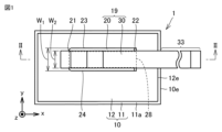
- FIG. 1 is a schematic plan view of a semiconductor device according to a first embodiment
- FIG. 2 is a schematic cross-sectional view of the semiconductor device of Embodiment 1 taken along the cross-sectional line II-II shown in FIG. 1.
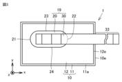
- FIG. 3 is a schematic plan view of a semiconductor device according to a modification of the first embodiment.
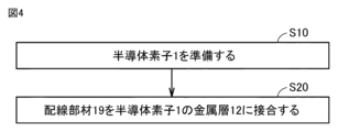
- FIG. 1 is a diagram showing a flowchart of a method for manufacturing a semiconductor device according to a first embodiment
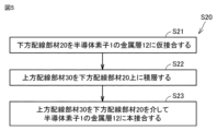
- FIG. FIG. 3 is a diagram showing a flowchart of a process of joining the wiring member of Embodiment 1 to a metal layer of a semiconductor element.
- 1 is a schematic cross-sectional view showing one step of the method for manufacturing a semiconductor device according to the first embodiment;
- FIG. 7 is a schematic cross-sectional view showing a step subsequent to the step shown in FIG. 6 in the method for manufacturing a semiconductor device according to the first embodiment.
- FIG. 8 is a schematic cross-sectional view showing a step subsequent to the step shown in FIG. 7 in the method for manufacturing a semiconductor device according to the first embodiment.
- FIG. 3 is a schematic cross-sectional view of a semiconductor device according to a modification of the first embodiment.
- FIG. 7 is a diagram showing a flowchart of a method for manufacturing a semiconductor device according to a modification of the first embodiment.
- FIG. FIG. 3 is a schematic plan view of a semiconductor device according to a second embodiment.
- FIG. 7 is a schematic plan view of a semiconductor device according to a third embodiment.
- FIG. 3 is a block diagram showing the configuration of a power conversion system according to a fourth embodiment.
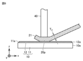
- Embodiment 1 A semiconductor device 1 according to a first embodiment will be described with reference to FIGS. 1 and 2.
- FIG. The semiconductor device 1 includes a semiconductor element 10 and a wiring member 19.
- the semiconductor device 10 is, for example, a power semiconductor device such as an insulated gate bipolar transistor (IGBT) or a metal oxide semiconductor field effect transistor (MOSFET).
- the semiconductor element 10 includes a semiconductor element body 11 and a metal layer 12.
- the semiconductor element body 11 is mainly formed of a semiconductor material such as silicon (Si), silicon carbide (SiC), or gallium nitride (GaN).
- a transistor structure including a p-type layer and an n-type layer is built into the semiconductor element body 11.
- the semiconductor element body 11 has a main surface 11a.
- the main surface 11a extends, for example, in the x direction and the y direction perpendicular to the x direction.
- the normal direction of the main surface 11a is the z direction perpendicular to the x direction and the y direction.
- the main surface 11a of the semiconductor element body 11 is formed of, for example, a semiconductor layer, an insulating layer, or a conductive layer.
- the semiconductor element 10 has an outer edge 10e.
- the outer edge 10e of the semiconductor element 10 is, for example, the outer edge of the main surface 11a.
- the metal layer 12 is provided on the main surface 11a of the semiconductor element body 11.
- the metal layer 12 is a conductive layer to which the wiring member 19 is bonded, and is, for example, an electrode, a wiring layer, or a conductive pad of the semiconductor element 10.
- the metal layer 12 is formed of, for example, Al, Cu, Ni, W, Co, Cr, or Ti, or an alloy of at least two of these elements.
- the thickness of the metal layer 12 is not particularly limited, but is, for example, 1 ⁇ m or more and 50 ⁇ m or less. In a plan view of the main surface 11a of the semiconductor element body 11, the metal layer 12 has an outer edge 12e.
- a diffusion barrier layer (not shown) or an adhesion layer (not shown) may be provided between the semiconductor element body 11 and the metal layer 12.
- the diffusion barrier layer prevents metal atoms forming the metal layer 12 from diffusing into the semiconductor element body 11.
- the adhesion layer improves the adhesion between the semiconductor element body 11 and the metal layer 12.
- the diffusion barrier layer and the adhesion layer are made of, for example, W, Co, Cr, Ti, Pd, or Pt, or an alloy of at least two of these metal elements.
- An anti-oxidation film (not shown) may be provided on the surface of the metal layer 12 exposed from the semiconductor element body 11. The anti-oxidation film prevents the metal layer 12 from being oxidized.
- the antioxidant film is made of, for example, an organic material or an inorganic material.
- the inorganic material used for the antioxidant film is, for example, a metal material such as Au, Ag, Pd, or Pt.
- the wiring member 19 is bonded to the metal layer 12 of the semiconductor element 10.
- the wiring member 19 includes a lower wiring member 20 and an upper wiring member 30.
- the lower wiring member 20 and the upper wiring member 30 are formed of a conductive material containing copper or aluminum as a main component.
- the lower wiring member 20 and the upper wiring member 30 are, for example, conductive wires or conductive ribbons.
- the lower wiring member 20 is arranged between the metal layer 12 of the semiconductor element 10 and the upper wiring member 30.
- the lower wiring member 20 is joined to the metal layer 12 and the upper wiring member 30.
- the lower wiring member 20 is ultrasonically bonded to the metal layer 12 and the upper wiring member 30.
- the lower wiring member 20 includes a first portion 26 that is in contact with the upper wiring member 30 and a second portion 27 that is spaced from the upper wiring member 30.
- the minimum thickness T 1 of the first portion 26 is smaller than the maximum thickness T 2 of the second portion 27 .
- the maximum thickness of the second portion 27 is the thickness of the lower wiring member 20 before the upper wiring member 30 is bonded to the metal layer 12 of the semiconductor element 10 via the lower wiring member 20 (see FIG. 7); This is the thickness of the conductive wiring member 20p (see FIG. 6).
- the maximum thickness T2 of the second portion 27 is, for example, 100 ⁇ m or more.
- the lower wiring member 20 may have an elongated shape in the longitudinal direction (x direction) of the upper wiring member 30.
- the shape of the lower wiring member 20 may be, for example, approximately rectangular (see FIG. 1), or may be a shape in which semicircles are combined on both short sides of a rectangle (see FIG. 3). , may be oval or polygonal.
- the shape of the lower wiring member 20 may be, for example, a square, a circle, or a regular polygon.
- the lower wiring member 20 includes an end surface 21 and an end surface 22 opposite to the end surface 21.
- the end surface 21 and the end surface 22 are both end surfaces of the lower wiring member 20 in the longitudinal direction (x direction) of the upper wiring member 30.
- the lower wiring member 20 has an elongated shape in the longitudinal direction of the upper wiring member 30 in a plan view of the main surface 11a of the semiconductor element body 11, the end face 21 and the end face 22 are both end faces of the lower wiring member 20 in the longitudinal direction. be.
- At least one of the end surfaces 21 and 22 is a cut end surface.
- the cut end surface is an end surface formed by cutting the conductive wiring member 20p (for example, a conductive wire or a conductive ribbon) with a cutter 42, as shown in FIG.
- end surface 22 is a cut end surface.
- the end surface 21 may also be a cut end surface.
- the end surface 21 and the end surface 22 may each be a flat surface or a curved surface.
- the lower wiring member 20 in a plan view of the main surface 11a of the semiconductor element body 11, includes an edge 23 and an edge 24. Edge 23 and edge 24 are connected to end surface 21 and end surface 22, respectively. The edges 23 and 24 extend in the longitudinal direction (x direction) of the upper wiring member 30. The edges 23 and 24 face each other in the lateral direction (y direction) of the upper wiring member 30. In a plan view of the main surface 11 a of the semiconductor element body 11 , the lateral direction of the upper wiring member 30 is perpendicular to the longitudinal direction of the upper wiring member 30 .
- the edges 23 and 24 each extend in the longitudinal direction of the lower wiring member 20. There is.
- the lower wiring member 20 has an elongated shape in the longitudinal direction of the upper wiring member 30 in a plan view of the main surface 11a of the semiconductor element body 11, the edges 23 and 24 are opposed to each other in the lateral direction of the lower wiring member 20. are doing.
- the lateral direction of the lower wiring member 20 is perpendicular to the longitudinal direction of the lower wiring member 20 .
- the end face 21 and the end face 22 of the lower wiring member 20 are located inside the outer edge 10e of the semiconductor element 10.
- the end surface 21 and the end surface 22 of the lower wiring member 20 may be located inside the outer edge 10 e of the metal layer 12 .
- the upper wiring member 30 is stacked on the lower wiring member 20.
- the upper wiring member 30 is joined to the metal layer 12 via the lower wiring member 20.
- the metal layer 12, the lower wiring member 20, and the upper wiring member 30 are laminated in the normal direction (z direction) of the main surface 11a of the semiconductor element body 11.
- a portion 33 of the upper wiring member 30 is located outside the outer edge 10e of the semiconductor element 10.
- a portion 33 of the upper wiring member 30 is located outside the outer edge 10 e of the metal layer 12 .
- a portion 33 of the upper wiring member 30 is bonded to another semiconductor element 10 (not shown) or a circuit pattern (not shown).
- the longitudinal direction of the upper wiring member 30 is 20 along the longitudinal direction.
- the longitudinal direction of the upper wiring member 30 may be parallel to the longitudinal direction of the lower wiring member 20, or may be non-parallel.
- the angle between the longitudinal direction of the upper wiring member 30 and the longitudinal direction of the lower wiring member 20 is 0° or more and less than 45°. This angle may be 30° or less, 20° or less, or 10° or less.
- the width W2 of the upper wiring member 30 in the lateral direction of the upper wiring member 30 is the width W2 of the lower wiring member 30 in the lateral direction of the upper wiring member 30.
- the width W of the member 20 is smaller than 1 .
- the portion 28 of the upper wiring member 30 between the end face 21 and the end face 22 of the lower wiring member 20 is located in the lateral direction of the upper wiring member 30 (for example, in the y direction). ) overlaps the lower wiring member 20 .
- the width of the portion 28 of the upper wiring member 30 between the end face 21 and the end face 22 of the lower wiring member 20 in the short direction of the upper wiring member 30 is The entire portion is located between the edges 23 and 24 of the lower wiring member 20.
- the portion 28 of the upper wiring member 30 located between the end face 21 and the end face 22 of the lower wiring member 20 is the lower wiring member in the lateral direction of the upper wiring member 30. It doesn't go beyond 20.
- the method for manufacturing semiconductor device 1 includes preparing semiconductor element 10 (S10).
- the semiconductor element 10 includes a semiconductor element body 11 and a metal layer 12.
- the semiconductor element body 11 has a main surface 11a.
- the metal layer 12 is provided on the main surface 11a of the semiconductor element 10.
- the metal layer 12 is formed, for example, by chemical vapor deposition (CVD), physical vapor deposition (PVD) such as sputtering, or plating.
- Preparing the semiconductor device 10 includes, for example, manufacturing the semiconductor device 10 using a known manufacturing method or purchasing the semiconductor device 10.
- the method for manufacturing semiconductor device 1 includes bonding wiring member 19 to metal layer 12 of semiconductor element 10 (S20).
- the wiring member 19 includes a lower wiring member 20 and an upper wiring member 30.
- joining the wiring member 19 to the metal layer 12 of the semiconductor element 10 (S20) includes temporarily joining the lower wiring member 20 to the metal layer 12 of the semiconductor element 10 (S21).
- a conductive wiring member 20p is laminated on the metal layer 12 of the semiconductor element 10.
- the conductive wiring member 20p includes an end surface 21.
- the conductive wiring member 20p is made of the same material as the lower wiring member 20, but is longer than the lower wiring member 20.
- the conductive wiring member 20p is temporarily joined to the metal layer 12 of the semiconductor element 10 using the ultrasonic horn 40.
- the conductive wiring member 20p is connected to the semiconductor element 10 while applying a first load and first ultrasonic vibration energy to the conductive wiring member 20p using the ultrasonic horn 40. Ultrasonic bonding is performed to the metal layer 12.
- the conductive wiring member 20p is cut using the cutter 42. In this way, the lower wiring member 20 temporarily bonded to the metal layer 12 of the semiconductor element 10 is obtained.
- the lower wiring member 20 includes an end surface 21 and an end surface 22 opposite to the end surface 21.
- the end surface 22 of the lower wiring member 20 is a cut end surface.
- the end face 21 and the end face 22 are both end faces of the lower wiring member 20 in the longitudinal direction of the lower wiring member 20.
- the end face 21 and the end face 22 are located inside the outer edge 10e of the semiconductor element 10. Then, the ultrasonic horn 40 and cutter 42 are separated from the lower wiring member 20.
- joining the wiring member 19 to the metal layer 12 of the semiconductor element 10 includes stacking the upper wiring member 30 on the lower wiring member 20 (S22).
- a portion 33 of the upper wiring member 30 is located outside the outer edge 10e of the semiconductor element 10.
- the end surface 21 and the end surface 22 are both end surfaces of the lower wiring member 20 in the longitudinal direction (x direction) of the upper wiring member 30.
- joining the wiring member 19 to the metal layer 12 of the semiconductor element 10 means connecting the upper wiring member 30 to the metal layer 12 of the semiconductor element 10 via the lower wiring member 20.
- the upper wiring member 30 is connected to the upper wiring member 30 via the lower wiring member 20 while applying a second load and second ultrasonic vibration energy to the upper wiring member 30 using the ultrasonic horn 40. Ultrasonic bonding is performed to the metal layer 12 of the semiconductor element 10.
- the second load in the main bonding step (S23) is greater than the first load in the temporary bonding step (S21), or the second ultrasonic vibration energy in the main bonding step (S23) is greater than the first load in the temporary bonding step (S21). Smaller than sound wave vibration energy.
- the upper wiring member 30 is permanently bonded to the metal layer 12 of the semiconductor element 10 via the lower wiring member 20.
- both the upper wiring member 30 and the lower wiring member 20 are wiring members. Therefore, a similar bonding method such as ultrasonic bonding may be employed in the temporary bonding step (S21) and the main bonding step (S23). The productivity of the semiconductor device 1 is improved.
- the first load in the temporary bonding step (S21) is smaller than the second load in the main bonding step (S23), or the first ultrasonic vibration energy in the temporary bonding step (S21) is lower than the second load in the main bonding step (S23). It is smaller than the second ultrasonic vibration energy in step (S23). Therefore, damage to the semiconductor element 10 is prevented in the temporary bonding step (S21). Further, in the main bonding step (S23), the lower wiring member 20 is arranged between the metal layer 12 of the semiconductor element 10 and the upper wiring member 30.
- semiconductor device 1 further includes an insulating sealing member 50.
- the insulating sealing member 50 seals the semiconductor element 10, the lower wiring member 20, and the upper wiring member 30.
- the insulating sealing member 50 is made of an insulating resin material such as, for example, epoxy resin, polyimide resin, polyamide resin, polyamideimide resin, fluorine resin, isocyanate resin, or silicone resin.
- a method for manufacturing the semiconductor device 1 according to a modification of the present embodiment will be described with reference to FIG. 10.
- the method for manufacturing the semiconductor device 1 according to the modification of the present embodiment includes the same steps as the method for manufacturing the semiconductor device 1 according to the present embodiment shown in FIGS. 4 and 5, but mainly includes the following points. This is different from the method of manufacturing the semiconductor device 1 of this embodiment.
- the method for manufacturing the semiconductor device 1 according to the modification of the present embodiment further includes sealing the semiconductor element 10, the lower wiring member 20, and the upper wiring member 30 with an insulating sealing member 50 (S30). Step S30 is performed after step S20. Specifically, the semiconductor element 10 to which the upper wiring member 30 is bonded via the lower wiring member 20 is placed in a cavity of a frame (not shown).
- This frame corresponds to a metal mold in the case of a mold type, and corresponds to a case in the case of a case type.
- the insulating sealing member 50 is formed by curing the sealing resin. In this way, the semiconductor element 10, the lower wiring member 20, and the upper wiring member 30 are sealed with the insulating sealing member 50.
- the semiconductor device 1 of this embodiment includes a semiconductor element 10, a lower wiring member 20, and an upper wiring member 30.
- the semiconductor element 10 includes a semiconductor element body 11 having a main surface 11a, and a metal layer 12 provided on the main surface 11a.
- the lower wiring member 20 includes a first end surface (end surface 21) and a second end surface (end surface 22) opposite to the first end surface.
- the first end surface and the second end surface are both end surfaces of the lower wiring member 20 in the longitudinal direction of the upper wiring member 30.
- the first end surface and the second end surface are located inside the outer edge 10 e of the semiconductor element 10 .
- the upper wiring member 30 is laminated on the lower wiring member 20.
- a portion 33 of the upper wiring member 30 is located outside the outer edge 10e of the semiconductor element 10.
- the upper wiring member 30 is joined to the metal layer 12 via the lower wiring member 20.
- both the upper wiring member 30 and the lower wiring member 20 are wiring members, the upper wiring member 30 and the lower wiring member 20 can be joined using the same joining method. Therefore, the productivity of the semiconductor device 1 is improved. Further, since the lower wiring member 20 is disposed between the metal layer 12 of the semiconductor element 10 and the upper wiring member 30, damage to the semiconductor element 10 is prevented when the upper wiring member 30 is bonded. . The reliability of the semiconductor device 1 is improved. Furthermore, in a plan view of the main surface 11a of the semiconductor element body 11, the first end surface (end surface 21) and the second end surface (end surface 22) of the lower wiring member 20 are located inside the outer edge 10e of the semiconductor element 10.
- At least one of the first end surface (end surface 21) or the second end surface (end surface 22) is a cut end surface. Therefore, the reliability and productivity of the semiconductor device 1 are improved.
- the metal layer 12 and the lower wiring member 20 are ultrasonically bonded to each other.
- the lower wiring member 20 and the upper wiring member 30 are ultrasonically bonded to each other. Therefore, the reliability and productivity of the semiconductor device 1 are improved.
- the lower wiring member 20 includes a first portion 26 that is in contact with the upper wiring member 30 and a second portion 27 that is separated from the upper wiring member 30.
- the minimum thickness T 1 of the first portion 26 is smaller than the maximum thickness T 2 of the second portion 27 . Therefore, the heat generated in the upper wiring member 30 can be efficiently radiated.
- the maximum thickness T2 of the second portion 27 is 100 ⁇ m or more. Therefore, the reliability and productivity of the semiconductor device 1 are improved.
- the lower wiring member 20 has an elongated shape in a plan view of the main surface 11a, and the longitudinal direction of the upper wiring member 30 is along the longitudinal direction of the lower wiring member 20. ing.
- the contact area between the upper wiring member 30 and the lower wiring member 20 increases. Damage to the semiconductor element 10 when joining the upper wiring member 30 is further prevented. The reliability of the semiconductor device 1 is improved.
- the upper wiring located between the first end surface (end surface 21) and the second end surface (end surface 22) of the lower wiring member 20 in a plan view of the main surface 11a of the semiconductor element body 11
- the entire width of the portion 28 of the member 30 in the lateral direction of the upper wiring member 30 overlaps with the lower wiring member 20.
- the lateral direction of the upper wiring member 30 is perpendicular to the longitudinal direction of the upper wiring member 30 in a plan view of the main surface 11a of the semiconductor element body 11.
- the contact area between the upper wiring member 30 and the lower wiring member 20 increases. Damage to the semiconductor element 10 when joining the upper wiring member 30 is further prevented. The reliability of the semiconductor device 1 is improved.
- the lower wiring member 20 and the upper wiring member 30 are formed of a conductive material containing copper or aluminum as a main component. Therefore, the reliability and productivity of the semiconductor device 1 are improved.
- the lower wiring member 20 and the upper wiring member 30 are conductive wires or conductive ribbons. Therefore, the reliability and productivity of the semiconductor device 1 are improved.
- the semiconductor device 1 of this embodiment further includes an insulating sealing member 50 that seals the semiconductor element 10, the lower wiring member 20, and the upper wiring member 30.
- the semiconductor element 10, lower wiring member 20, and upper wiring member 30 are protected by an insulating sealing member 50. Further, since the first end surface (end surface 21) and the second end surface (end surface 22) of the lower wiring member 20 are located inside the outer edge 10e of the semiconductor element 10, the lower wiring member 20 is short. Therefore, the contact area between the lower wiring member 20 and the insulating sealing member 50 is reduced. The stress applied to the lower wiring member 20 is reduced due to the difference between the coefficient of thermal expansion of the lower wiring member 20 and the thermal expansion coefficient of the insulating sealing member 50. The lower wiring member 20 is less likely to peel off from the metal layer 12 during use of the semiconductor device 1.
- the lower wiring member 20 is short, the force that the lower wiring member 20 receives from the sealing resin flowing when the sealing resin is injected is reduced.
- the bonding strength between the lower wiring member 20 and the metal layer 12 can be prevented from decreasing. In this way, the reliability of the semiconductor device 1 is improved.
- the method for manufacturing the semiconductor device 1 of this embodiment includes temporarily bonding the lower wiring member 20 to the metal layer 12 of the semiconductor element 10 (S21).
- the semiconductor element 10 includes a semiconductor element body 11 having a main surface 11a, and a metal layer 12 provided on the main surface 11a.
- the lower wiring member 20 includes a first end surface (end surface 21) and a second end surface (end surface 22) opposite to the first end surface. In a plan view of the principal surface 11 a of the semiconductor element body 11 , the first end surface and the second end surface are located inside the outer edge 10 e of the semiconductor element 10 .
- the method for manufacturing the semiconductor device 1 of this embodiment includes stacking the upper wiring member 30 on the lower wiring member 20 (S22).
- a portion 33 of the upper wiring member 30 is located outside the outer edge 10e of the semiconductor element 10.
- the first end surface and the second end surface are both end surfaces of the lower wiring member 20 in the longitudinal direction of the upper wiring member 30.
- the method for manufacturing the semiconductor device 1 according to the present embodiment includes main bonding of the upper wiring member 30 to the metal layer 12 of the semiconductor element 10 via the lower wiring member 20 (S23).
- both the upper wiring member 30 and the lower wiring member 20 are wiring members, the upper wiring member 30 and the lower wiring member 20 can be joined using the same joining method. Therefore, the productivity of the semiconductor device 1 is improved. Further, since the lower wiring member 20 is disposed between the metal layer 12 of the semiconductor element 10 and the upper wiring member 30, damage to the semiconductor element 10 is prevented when the upper wiring member 30 is bonded. . The reliability of the semiconductor device 1 is improved. Furthermore, in a plan view of the main surface 11a of the semiconductor element body 11, the first end surface (end surface 21) and the second end surface (end surface 22) of the lower wiring member 20 are located inside the outer edge 10e of the semiconductor element 10. Therefore, the semiconductor element 10 can be prevented from shorting to a conductive member (for example, an electrode of another semiconductor element or another wiring member) around the semiconductor element 10 through the lower wiring member 20. The reliability of the semiconductor device 1 is improved.
- temporarily bonding the lower wiring member 20 to the metal layer 12 of the semiconductor element 10 involves applying a first load to the lower wiring member 20 and applying a first ultrasonic vibration energy to the lower wiring member 20.
- the lower wiring member 20 is ultrasonically bonded to the metal layer 12 of the semiconductor element 10 while applying .
- Mainly bonding the upper wiring member 30 to the metal layer 12 of the semiconductor element 10 via the lower wiring member 20 involves applying the second load and the second ultrasonic vibration energy to the upper wiring member 30 while This involves ultrasonically bonding the wiring member 30 to the metal layer 12 of the semiconductor element 10 via the lower wiring member 20.
- the first load is less than the second load, or the first ultrasonic vibration energy is less than the second ultrasonic vibration energy.
- the method for manufacturing the semiconductor device 1 of this embodiment further includes sealing the semiconductor element 10, the lower wiring member 20, and the upper wiring member 30 with an insulating sealing member 50 (S30).
- the semiconductor element 10, lower wiring member 20, and upper wiring member 30 are protected by an insulating sealing member 50. Further, since the first end surface (end surface 21) and the second end surface (end surface 22) of the lower wiring member 20 are located inside the outer edge 10e of the semiconductor element 10, the lower wiring member 20 is short. Therefore, the contact area between the lower wiring member 20 and the insulating sealing member 50 is reduced. The stress applied to the lower wiring member 20 is reduced due to the difference between the coefficient of thermal expansion of the lower wiring member 20 and the thermal expansion coefficient of the insulating sealing member 50. The lower wiring member 20 is less likely to peel off from the metal layer 12 during use of the semiconductor device 1.
- the lower wiring member 20 is short, the force that the lower wiring member 20 receives from the sealing resin flowing when the sealing resin is injected is reduced.
- the bonding strength between the lower wiring member 20 and the metal layer 12 can be prevented from decreasing. In this way, the reliability of the semiconductor device 1 is improved.
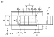
- Embodiment 2 With reference to FIG. 11, a semiconductor device 1b according to a second embodiment will be described.
- the semiconductor device 1b of this embodiment has the same configuration as the semiconductor device 1 of the first embodiment, but differs mainly in the following points.
- the width W 2 of the upper wiring member 30 in this embodiment is larger than the width W 2 of the upper wiring member 30 in the first embodiment. Therefore, in the semiconductor device 1b of this embodiment, a larger current can flow through the semiconductor element 10 than in the semiconductor device 1 of the first embodiment.
- the lower wiring member 20 includes a plurality of lower wirings 20a, 20b, and 20c arranged in the lateral direction (y direction) of the upper wiring member 30.
- Each of the plurality of lower wirings 20a, 20b, and 20c is formed of a conductive material containing copper or aluminum as a main component, similarly to the lower wiring member 20 of the first embodiment.
- Each of the plurality of lower wirings 20a, 20b, 20c is, for example, a conductive wire or a conductive ribbon.
- each of the plurality of lower wirings 20a, 20b, and 20c may have an elongated shape in the longitudinal direction of the upper wiring member 30.
- Each of the plurality of lower wirings 20a, 20b, 20c includes both end surfaces similarly to the lower wiring member 20 of Embodiment 1, and at least one of the both end surfaces of each of the plurality of lower wirings 20a, 20b, 20c is , is the cut end surface.
- the lower wiring 20a includes an end surface 21a and an end surface 22a on the opposite side to the end surface 21a. At least one of the end surfaces 21a and 22a is a cut end surface.
- the lower wiring 20b includes an end surface 21b and an end surface 22b opposite to the end surface 21b. At least one of the end surfaces 21b and 22b is a cut end surface.
- the lower wiring 20c includes an end surface 21c and an end surface 22c opposite to the end surface 21c.
- At least one of the end surfaces 21c and 22c is a cut end surface.
- the end surfaces 22a, 22b, and 22c are cut end surfaces.
- the end surfaces 21a, 21b, and 21c may also be cut end surfaces.
- the end surface 21 of the lower wiring member 20 includes an end surface 21a of the lower wiring 20a, an end surface 21b of the lower wiring 20b, and an end surface 21c of the lower wiring 20c.
- the end surface 22 of the lower wiring member 20 includes an end surface 22a of the lower wiring 20a, an end surface 22b of the lower wiring 20b, and an end surface 22c of the lower wiring 20c.
- Each of the plurality of lower wirings 20a, 20b, and 20c has a width W3 smaller than the width W2 of the upper wiring member 30.
- the upper wiring member 30 is disposed astride the plurality of lower wirings 20a, 20b, and 20c. Therefore, even if the width W 1 of the upper wiring member 30 increases, the portion of the upper wiring member 30 that is between the end surface 21 and the end surface 22 of the lower wiring member 20 in a plan view of the main surface 11a of the semiconductor element body 11 28 does not protrude from the lower wiring member 20 in the lateral direction of the upper wiring member 30.
- the method for manufacturing the semiconductor device 1b of this embodiment includes the same steps as the method for manufacturing the semiconductor device 1 of the first embodiment, but differs mainly in the following points.
- a plurality of lower wirings 20a, 20b, 20c are temporarily bonded to the metal layer 12 of the semiconductor element 10 in the temporary bonding step (S21) shown in FIG.
- the lamination step (S22) shown the upper wiring member 30 is laminated on the plurality of lower wirings 20a, 20b, 20c, and in the main bonding step (S23) shown in FIG. Main bonding is made to the metal layer 12 of the semiconductor element 10 via 20b and 20c.
- the semiconductor device 1b and its manufacturing method of the present embodiment have the following effects.
- the lower wiring member 20 includes a plurality of lower wirings 20a, 20b, and 20c arranged in the lateral direction of the upper wiring member 30.
- the lateral direction (y direction) of the upper wiring member 30 is perpendicular to the longitudinal direction (x direction) of the upper wiring member 30 in a plan view of the main surface 11a of the semiconductor element body 11.
- the upper wiring member 30 is disposed astride the plurality of lower wirings 20a, 20b, and 20c.
- the plurality of lower wirings 20a, 20b, 20c can be reliably connected between the upper wiring member 30 and the metal layer 12. can be interposed. Damage to the semiconductor element 10 is prevented when the upper wiring member 30 is bonded. The reliability of the semiconductor device 1b is improved.
- Embodiment 3 Referring to FIG. 12, a semiconductor device 1c according to the third embodiment will be described.
- the semiconductor device 1c of this embodiment has the same configuration as the semiconductor device 1 of the first embodiment, but differs mainly in the following points.
- the upper wiring member 30 includes a plurality of upper wirings 30a and 30b arranged in the lateral direction (y direction) of the upper wiring member 30.
- Each of the plurality of upper wirings 30a, 30b is formed of a conductive material containing copper or aluminum as a main component, similarly to the upper wiring member 30 of the first embodiment.
- Each of the plurality of upper wirings 30a, 30b is, for example, a conductive wire or a conductive ribbon.
- each of the plurality of upper wirings 30a, 30b has an elongated shape in the longitudinal direction of the upper wiring member 30. Since the plurality of upper wirings 30a and 30b are arranged in parallel, in the semiconductor device 1c of this embodiment, a larger current can flow through the semiconductor element 10 than in the semiconductor device 1 of the first embodiment.
- the width W 1 of the lower wiring member 20 of the present embodiment is larger than the width W 1 of the lower wiring member 20 of the first embodiment so that the plurality of upper wirings 30 a and 30 b can be stacked on the lower wiring member 20 .
- Each of the plurality of upper wirings 30a, 30b has a width W4 smaller than the width W1 of the lower wiring member 20.
- the plurality of upper wirings 30a, 30b are arranged on the lower wiring member 20.
- the lower wiring member 20 is disposed astride the plurality of upper wirings 30a, 30b.
- the upper wiring member 30 located between the end face 21 and the end face 22 of the lower wiring member 20 in a plan view of the main surface 11a of the semiconductor element body 11 The portion 28 does not protrude from the lower wiring member 20 in the lateral direction of the upper wiring member 30.
- the method for manufacturing the semiconductor device 1c of this embodiment includes the same steps as the method for manufacturing the semiconductor device 1 of the first embodiment, but differs mainly in the following points. In the method for manufacturing the semiconductor device 1c of this embodiment, in the main bonding step (S23) shown in FIG. do.
- the semiconductor device 1c and its manufacturing method of the present embodiment have the following effects.
- the upper wiring member 30 includes a plurality of upper wirings 30a and 30b arranged in the lateral direction (y direction) of the upper wiring member 30.
- the lateral direction of the upper wiring member 30 is perpendicular to the longitudinal direction (x direction) of the upper wiring member 30 in a plan view of the main surface 11a of the semiconductor element body 11.
- the plurality of upper wirings 30a, 30b are arranged on the lower wiring member 20.
- the lower wiring member 20 can be reliably connected between the plurality of upper wirings 30a, 30b and the metal layer 12. can be interposed. Damage to the semiconductor element 10 is prevented when the plurality of upper wirings 30a, 30b are bonded together. The reliability of the semiconductor device 1c is improved.
- the width W1 of the lower wiring member 20 is increased so that the plurality of upper wirings 30a and 30b can be stacked.
- the bonding area between the lower wiring member 20 and the metal layer 12 increases. Even if thermal stress is repeatedly applied to the joint between the lower wiring member 20 and the metal layer 12 during use of the semiconductor device 1c, it takes a longer time until the lower wiring member 20 is separated by cracks. Therefore, the reliability of the semiconductor device 1c is improved.
- a semiconductor device of a comparative example includes a plurality of upper wirings 30a, 30b and a plurality of lower wirings 20a, 20b, 20c, and connects each of the plurality of upper wirings 30a, 30b with a corresponding lower wiring (see FIG. 11).
- the semiconductor device 1c of this embodiment the number of joints between the lower wiring member and the metal layer is reduced. As the number of joints decreases, the risk of damage to the joints due to thermal stress during use of the semiconductor device 1c decreases, and the productivity of the semiconductor device 1c improves. Therefore, the reliability and productivity of the semiconductor device 1c are improved.
- Embodiment 4 the semiconductor devices 1, 1b, and 1c of the first to third embodiments described above are applied to a power conversion device.
- the present disclosure is not limited to a specific power conversion device, a case will be described below as a fourth embodiment in which the semiconductor devices 1, 1b, and 1c of the present disclosure are applied to a three-phase inverter.
- the power conversion system shown in FIG. 13 includes a power source 100, a power conversion device 200, and a load 300.
- Power supply 100 is a DC power supply and supplies DC power to power conversion device 200.
- the power supply 100 is not particularly limited, and may be configured with, for example, a DC system, a solar battery, or a storage battery, or may be configured with a rectifier circuit or an AC/DC converter connected to an AC system.
- Power supply 100 may be configured with a DC/DC converter that converts DC power output from a DC system into other DC power.
- the power conversion device 200 is a three-phase inverter connected between the power source 100 and the load 300, converts the DC power supplied from the power source 100 into AC power, and supplies the AC power to the load 300. As shown in FIG. 13, the power conversion device 200 includes a main conversion circuit 201 that converts DC power into AC power and outputs it, and a control circuit that outputs a control signal for controlling the main conversion circuit 201 to the main conversion circuit 201. 203.
- the load 300 is a three-phase electric motor driven by AC power supplied from the power conversion device 200.
- the load 300 is not limited to a specific application, but is a motor installed in various electrical devices, and is used, for example, as a motor for a hybrid vehicle, an electric vehicle, a railway vehicle, an elevator, or an air conditioner.
- the main conversion circuit 201 includes a switching element (not shown) and a free wheel diode (not shown). By switching the voltage supplied from the power supply 100 by the switching element, the main conversion circuit 201 converts the DC power supplied from the power supply 100 into AC power, and supplies the alternating current power to the load 300 .
- the main conversion circuit 201 of this embodiment is a two-level three-phase full bridge circuit, and has six switching elements and each switching element has a reverse circuit configuration. It can be composed of six freewheeling diodes connected in parallel.
- At least one of the switching elements of the main conversion circuit 201 is a switching element included in the semiconductor device 202 corresponding to the semiconductor device 1, 1b, or 1c of any one of the first to third embodiments described above.
- the six switching elements are connected in series every two switching elements to constitute upper and lower arms, and each upper and lower arm constitutes each phase (U phase, V phase, W phase) of the full bridge circuit.
- the output terminals of the upper and lower arms, that is, the three output terminals of the main conversion circuit 201, are connected to the load 300.
- the main conversion circuit 201 also includes a drive circuit (not shown) that drives each switching element.
- the drive circuit may be built into the semiconductor device 202 or may be provided outside the semiconductor device 202.
- the drive circuit generates a drive signal to drive the switching element of the main conversion circuit 201 and supplies the drive signal to the control electrode of the switching element of the main conversion circuit 201. Specifically, according to a control signal from the control circuit 203, a drive signal that turns the switching element on and a drive signal that turns the switching element off are output to the control electrode of each switching element.
- the drive signal When keeping the switching element in the on state, the drive signal is a voltage signal (on signal) that is greater than or equal to the threshold voltage of the switching element, and when the switching element is kept in the off state, the drive signal is a voltage signal that is less than or equal to the threshold voltage of the switching element. signal (off signal).
- the control circuit 203 controls the switching elements of the main conversion circuit 201 so that power is supplied to the load 300. Specifically, based on the power to be supplied to the load 300, the time (on time) during which each switching element of the main conversion circuit 201 should be in the on state is calculated. For example, the main conversion circuit 201 can be controlled by PWM control that modulates the on-time of the switching element according to the voltage to be output to the load 300. Then, a control command (control signal) is given to the drive circuit included in the main conversion circuit 201 so that an on signal is output to the switching element that should be in the on state at each time, and an off signal is output to the switching element that should be in the off state. Output. The drive circuit outputs an on signal or an off signal as a drive signal to the control electrode of each switching element according to this control signal.
- any of the semiconductor devices 1, 1b, and 1c of Embodiments 1 to 3 is applied as the semiconductor device 202 that constitutes the main conversion circuit 201. Therefore, the reliability and productivity of the power conversion device can be improved.
- the present disclosure is not limited to this and can be applied to various power conversion devices.
- a two-level power converter is used in this embodiment, it may be a three-level power converter or a multi-level power converter, or when the power converter supplies power to a single-phase load.
- the present disclosure may be applied to a single-phase inverter.
- the present disclosure can be applied to a DC/DC converter or an AC/DC converter.
- the power conversion device to which the present disclosure is applied is not limited to the case where the above-mentioned load is an electric motor, but is used, for example, as a power supply device for an electric discharge machine, a laser processing machine, an induction heating cooker, or a non-contact power supply system. Furthermore, it can also be used as a power conditioner for solar power generation systems, power storage systems, etc.
- Embodiment 1 to Embodiment 4 disclosed this time should be considered to be illustrative in all respects and not restrictive.
- the scope of the present disclosure is indicated by the claims rather than the above description, and is intended to include meanings equivalent to the claims and all changes within the range.
- 1, 1b, 1c semiconductor device 10 semiconductor element, 10e outer edge, 11 semiconductor element body, 11a main surface, 12 metal layer, 12e outer edge, 19 wiring member, 20 lower wiring member, 20a, 20b, 20c lower wiring, 20p conductive Wiring member, 21, 21a, 21b, 21c, 22, 22a, 22b, 22c end face, 23, 24 edge, 26 first part, 27 second part, 28 part, 30 upper wiring member, 30a, 30b upper wiring, 33 Part, 40 ultrasonic horn, 42 cutter, 100 power supply, 200 power conversion device, 201 main conversion circuit, 202 semiconductor device, 203 control circuit, 300 load.
Landscapes
- Engineering & Computer Science (AREA)
- Power Engineering (AREA)
- Wire Bonding (AREA)
- Internal Circuitry In Semiconductor Integrated Circuit Devices (AREA)
Priority Applications (5)
| Application Number | Priority Date | Filing Date | Title |
|---|---|---|---|
| DE112022006886.8T DE112022006886T5 (de) | 2022-03-23 | 2022-03-23 | Halbleitervorrichtung und Verfahren zum Herstellen derselben und Leistungsumwandlungsvorrichtung |
| JP2023541088A JP7438466B1 (ja) | 2022-03-23 | 2022-03-23 | 半導体装置及びその製造方法並びに電力変換装置 |
| US18/845,441 US20250192098A1 (en) | 2022-03-23 | 2022-03-23 | Semiconductor apparatus and method for manufacturing the same, and power conversion apparatus |
| CN202280093758.7A CN118891704A (zh) | 2022-03-23 | 2022-03-23 | 半导体装置及其制造方法以及电力转换装置 |
| PCT/JP2022/013670 WO2023181210A1 (ja) | 2022-03-23 | 2022-03-23 | 半導体装置及びその製造方法並びに電力変換装置 |
Applications Claiming Priority (1)
| Application Number | Priority Date | Filing Date | Title |
|---|---|---|---|
| PCT/JP2022/013670 WO2023181210A1 (ja) | 2022-03-23 | 2022-03-23 | 半導体装置及びその製造方法並びに電力変換装置 |
Publications (1)
| Publication Number | Publication Date |
|---|---|
| WO2023181210A1 true WO2023181210A1 (ja) | 2023-09-28 |
Family
ID=88100567
Family Applications (1)
| Application Number | Title | Priority Date | Filing Date |
|---|---|---|---|
| PCT/JP2022/013670 Ceased WO2023181210A1 (ja) | 2022-03-23 | 2022-03-23 | 半導体装置及びその製造方法並びに電力変換装置 |
Country Status (5)
| Country | Link |
|---|---|
| US (1) | US20250192098A1 (https=) |
| JP (1) | JP7438466B1 (https=) |
| CN (1) | CN118891704A (https=) |
| DE (1) | DE112022006886T5 (https=) |
| WO (1) | WO2023181210A1 (https=) |
Citations (5)
| Publication number | Priority date | Publication date | Assignee | Title |
|---|---|---|---|---|
| JPH07169797A (ja) * | 1993-12-14 | 1995-07-04 | Hitachi Ltd | ボンディング方法及びボンディング構造 |
| WO2019008860A1 (ja) * | 2017-07-07 | 2019-01-10 | 三菱電機株式会社 | 半導体装置、及び半導体装置の製造方法 |
| JP2020113721A (ja) * | 2019-01-16 | 2020-07-27 | 富士電機株式会社 | 半導体装置および半導体装置の製造方法 |
| WO2020225097A1 (en) * | 2019-05-08 | 2020-11-12 | Danfoss Silicon Power Gmbh | Semiconductor module comprising a semiconductor body electrically contected to a shaped metal body, as well as the method of obtaining the same |
| WO2022029828A1 (ja) * | 2020-08-03 | 2022-02-10 | 三菱電機株式会社 | 半導体装置、半導体装置の製造方法および電力変換装置 |
Family Cites Families (1)
| Publication number | Priority date | Publication date | Assignee | Title |
|---|---|---|---|---|
| DE102014109766B3 (de) | 2014-07-11 | 2015-04-02 | Heraeus Deutschland GmbH & Co. KG | Verfahren zum Herstellen eines Substratadapters, Substratadapter und Verfahren zum Kontaktieren eines Halbleiterelements |
-
2022
- 2022-03-23 WO PCT/JP2022/013670 patent/WO2023181210A1/ja not_active Ceased
- 2022-03-23 JP JP2023541088A patent/JP7438466B1/ja active Active
- 2022-03-23 DE DE112022006886.8T patent/DE112022006886T5/de active Pending
- 2022-03-23 US US18/845,441 patent/US20250192098A1/en active Pending
- 2022-03-23 CN CN202280093758.7A patent/CN118891704A/zh active Pending
Patent Citations (5)
| Publication number | Priority date | Publication date | Assignee | Title |
|---|---|---|---|---|
| JPH07169797A (ja) * | 1993-12-14 | 1995-07-04 | Hitachi Ltd | ボンディング方法及びボンディング構造 |
| WO2019008860A1 (ja) * | 2017-07-07 | 2019-01-10 | 三菱電機株式会社 | 半導体装置、及び半導体装置の製造方法 |
| JP2020113721A (ja) * | 2019-01-16 | 2020-07-27 | 富士電機株式会社 | 半導体装置および半導体装置の製造方法 |
| WO2020225097A1 (en) * | 2019-05-08 | 2020-11-12 | Danfoss Silicon Power Gmbh | Semiconductor module comprising a semiconductor body electrically contected to a shaped metal body, as well as the method of obtaining the same |
| WO2022029828A1 (ja) * | 2020-08-03 | 2022-02-10 | 三菱電機株式会社 | 半導体装置、半導体装置の製造方法および電力変換装置 |
Also Published As
| Publication number | Publication date |
|---|---|
| DE112022006886T5 (de) | 2025-01-02 |
| CN118891704A (zh) | 2024-11-01 |
| JPWO2023181210A1 (https=) | 2023-09-28 |
| US20250192098A1 (en) | 2025-06-12 |
| JP7438466B1 (ja) | 2024-02-26 |
Similar Documents
| Publication | Publication Date | Title |
|---|---|---|
| US20200052449A1 (en) | Power semiconductor device and manufacturing method thereof, and power conversion device | |
| JP2018190930A (ja) | パワー半導体モジュール及びその製造方法並びに電力変換装置 | |
| JP6826665B2 (ja) | 半導体装置、半導体装置の製造方法及び電力変換装置 | |
| CN108538793B (zh) | 半导体功率模块及电力变换装置 | |
| JP6927437B1 (ja) | パワーモジュールおよび電力変換装置 | |
| JP7126609B2 (ja) | パワー半導体モジュール及び電力変換装置 | |
| CN111052325B (zh) | 半导体模块以及电力转换装置 | |
| US11107760B2 (en) | Semiconductor device, electric power conversion apparatus and method for manufacturing semiconductor device | |
| JP6965706B2 (ja) | 半導体モジュール、その製造方法及び電力変換装置 | |
| CN111788694B (zh) | 半导体元件、半导体装置、电力变换装置以及半导体元件的制造方法 | |
| JP7438466B1 (ja) | 半導体装置及びその製造方法並びに電力変換装置 | |
| JP6410998B1 (ja) | 半導体モジュール、半導体モジュールの製造方法および電力変換装置 | |
| JP2020043154A (ja) | 半導体装置及びその製造方法、並びに、電力変換装置 | |
| JP7088421B1 (ja) | 半導体装置および電力変換装置 | |
| WO2022130523A1 (ja) | 半導体装置、電力変換装置、および移動体 | |
| JP6742540B2 (ja) | 半導体装置及び電力変換装置 | |
| WO2023079640A1 (ja) | 半導体装置および電力変換装置 | |
| JP6885522B1 (ja) | 半導体装置、電力変換装置および半導体装置の製造方法 | |
| WO2025009015A1 (ja) | パワーモジュール及びその製造方法並びに電力変換装置 | |
| US20210320083A1 (en) | Manufacturing method of power semiconductor device, power semiconductor device, and power converter | |
| JP2026058632A (ja) | 電力用半導体装置および電力変換装置 | |
| WO2022064599A1 (ja) | 半導体装置および電力変換装置 | |
| WO2021070358A1 (ja) | 半導体装置、電力変換装置および半導体装置の製造方法 |
Legal Events
| Date | Code | Title | Description |
|---|---|---|---|
| WWE | Wipo information: entry into national phase |
Ref document number: 2023541088 Country of ref document: JP |
|
| 121 | Ep: the epo has been informed by wipo that ep was designated in this application |
Ref document number: 22933352 Country of ref document: EP Kind code of ref document: A1 |
|
| WWE | Wipo information: entry into national phase |
Ref document number: 18845441 Country of ref document: US |
|
| WWE | Wipo information: entry into national phase |
Ref document number: 202280093758.7 Country of ref document: CN |
|
| WWE | Wipo information: entry into national phase |
Ref document number: 112022006886 Country of ref document: DE |
|
| 122 | Ep: pct application non-entry in european phase |
Ref document number: 22933352 Country of ref document: EP Kind code of ref document: A1 |
|
| WWP | Wipo information: published in national office |
Ref document number: 18845441 Country of ref document: US |