WO2023171426A1 - コンデンサ - Google Patents
コンデンサ Download PDFInfo
- Publication number
- WO2023171426A1 WO2023171426A1 PCT/JP2023/006860 JP2023006860W WO2023171426A1 WO 2023171426 A1 WO2023171426 A1 WO 2023171426A1 JP 2023006860 W JP2023006860 W JP 2023006860W WO 2023171426 A1 WO2023171426 A1 WO 2023171426A1
- Authority
- WO
- WIPO (PCT)
- Prior art keywords
- conductive layer
- layer
- capacitor
- conductive
- dielectric layer
- Prior art date
- Legal status (The legal status is an assumption and is not a legal conclusion. Google has not performed a legal analysis and makes no representation as to the accuracy of the status listed.)
- Ceased
Links
Images


Classifications
-
- H—ELECTRICITY
- H01—ELECTRIC ELEMENTS
- H01G—CAPACITORS; CAPACITORS, RECTIFIERS, DETECTORS, SWITCHING DEVICES, LIGHT-SENSITIVE OR TEMPERATURE-SENSITIVE DEVICES OF THE ELECTROLYTIC TYPE
- H01G9/00—Electrolytic capacitors, rectifiers, detectors, switching devices, light-sensitive or temperature-sensitive devices; Processes of their manufacture
- H01G9/004—Details
- H01G9/022—Electrolytes; Absorbents
- H01G9/025—Solid electrolytes
- H01G9/032—Inorganic semiconducting electrolytes, e.g. MnO2
-
- H—ELECTRICITY
- H01—ELECTRIC ELEMENTS
- H01G—CAPACITORS; CAPACITORS, RECTIFIERS, DETECTORS, SWITCHING DEVICES, LIGHT-SENSITIVE OR TEMPERATURE-SENSITIVE DEVICES OF THE ELECTROLYTIC TYPE
- H01G9/00—Electrolytic capacitors, rectifiers, detectors, switching devices, light-sensitive or temperature-sensitive devices; Processes of their manufacture
- H01G9/004—Details
- H01G9/04—Electrodes or formation of dielectric layers thereon
- H01G9/042—Electrodes or formation of dielectric layers thereon characterised by the material
- H01G9/0425—Electrodes or formation of dielectric layers thereon characterised by the material specially adapted for cathode
-
- H—ELECTRICITY
- H01—ELECTRIC ELEMENTS
- H01G—CAPACITORS; CAPACITORS, RECTIFIERS, DETECTORS, SWITCHING DEVICES, LIGHT-SENSITIVE OR TEMPERATURE-SENSITIVE DEVICES OF THE ELECTROLYTIC TYPE
- H01G9/00—Electrolytic capacitors, rectifiers, detectors, switching devices, light-sensitive or temperature-sensitive devices; Processes of their manufacture
- H01G9/004—Details
- H01G9/04—Electrodes or formation of dielectric layers thereon
- H01G9/042—Electrodes or formation of dielectric layers thereon characterised by the material
- H01G9/045—Electrodes or formation of dielectric layers thereon characterised by the material based on aluminium
-
- H—ELECTRICITY
- H01—ELECTRIC ELEMENTS
- H01G—CAPACITORS; CAPACITORS, RECTIFIERS, DETECTORS, SWITCHING DEVICES, LIGHT-SENSITIVE OR TEMPERATURE-SENSITIVE DEVICES OF THE ELECTROLYTIC TYPE
- H01G9/00—Electrolytic capacitors, rectifiers, detectors, switching devices, light-sensitive or temperature-sensitive devices; Processes of their manufacture
- H01G9/004—Details
- H01G9/04—Electrodes or formation of dielectric layers thereon
- H01G9/048—Electrodes or formation of dielectric layers thereon characterised by their structure
-
- H—ELECTRICITY
- H01—ELECTRIC ELEMENTS
- H01G—CAPACITORS; CAPACITORS, RECTIFIERS, DETECTORS, SWITCHING DEVICES, LIGHT-SENSITIVE OR TEMPERATURE-SENSITIVE DEVICES OF THE ELECTROLYTIC TYPE
- H01G9/00—Electrolytic capacitors, rectifiers, detectors, switching devices, light-sensitive or temperature-sensitive devices; Processes of their manufacture
- H01G9/004—Details
- H01G9/07—Dielectric layers
-
- H—ELECTRICITY
- H01—ELECTRIC ELEMENTS
- H01G—CAPACITORS; CAPACITORS, RECTIFIERS, DETECTORS, SWITCHING DEVICES, LIGHT-SENSITIVE OR TEMPERATURE-SENSITIVE DEVICES OF THE ELECTROLYTIC TYPE
- H01G9/00—Electrolytic capacitors, rectifiers, detectors, switching devices, light-sensitive or temperature-sensitive devices; Processes of their manufacture
- H01G9/15—Solid electrolytic capacitors
Definitions
- the present disclosure relates to capacitors.
- Patent Document 1 Japanese Unexamined Patent Application Publication No. 2017-103412 describes, “an anode body, a dielectric layer disposed on the surface of the anode body, and a dielectric layer disposed on the surface of the dielectric layer, A solid electrolytic capacitor comprising: a solid electrolyte layer made of zinc oxide having a conductivity of .
- Patent Document 2 Japanese Unexamined Patent Publication No. 2020-35890 describes an anode body made of a valve metal, a dielectric layer formed on the surface of the anode body, and a semiconductor layer formed on the dielectric layer. , a cathode layer formed on the semiconductor layer, and the semiconductor layer is configured using a p-type inorganic semiconductor.''
- one of the objectives of the present disclosure is to provide a new capacitor that is highly resistant to high temperatures.
- the capacitor includes an anode body having a dielectric layer formed on its surface, and a conductive layer made of a metal oxide formed on the dielectric layer, the conductive layer being formed on the dielectric layer. and a second conductive layer formed on the first conductive layer, wherein the average thickness of the second conductive layer is greater than the average thickness of the first conductive layer. It's also big.
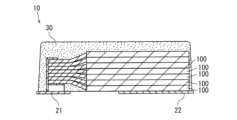
- FIG. 1 is a cross-sectional view schematically showing the structure of an example capacitor according to the present embodiment.
- 2 is a cross-sectional view schematically showing a part of the capacitor shown in FIG. 1.
- FIG. 3 is a cross-sectional view schematically showing the structure of another example of a capacitor according to the present embodiment.
- the capacitor according to this embodiment includes an anode body having a dielectric layer formed on its surface, and a conductive layer made of a metal oxide formed on the dielectric layer.
- the capacitor and the conductive layer may be hereinafter referred to as a "capacitor (C)" and a “conductive layer (L).”
- the conductive layer (L) includes a first conductive layer formed on the dielectric layer and a second conductive layer formed on the first conductive layer. The average thickness of the second conductive layer is greater than the average thickness of the first conductive layer.
- the capacitor (C) may further include a cathode extraction layer formed on the conductive layer and containing an inorganic conductive material. Since the capacitor (C) having this configuration does not include a solid electrolyte layer containing a conductive polymer, it has particularly high resistance to high temperatures.
- the average thickness T1 of the first conductive layer may be 1 nm or more, or 5 nm or more, or 1 ⁇ m, 500 nm or less, 100 nm or less, or 50 nm or less.
- the average thickness T1 of the first conductive layer may be in the range of 1 nm to 1 ⁇ m, or in the range of 5 nm to 1 ⁇ m. In any of these ranges, the upper limit may be 500 nm, 100 nm, or 50 nm.
- the average thickness T2 of the second conductive layer may be 50 nm or more, or 100 nm or more, and may be 50 ⁇ m or less, 20 ⁇ m or less, or 1 ⁇ m or less.
- the ratio T2/T1 between the average thickness T2 of the second conductive layer and the average thickness T1 of the first conductive layer is greater than 1, and may be greater than or equal to 10, greater than or equal to 1000, and less than or equal to 100000. , or 10,000 or less.
- the average thickness T1 of the first conductive layer can be measured as follows. First, a cross section of the first conductive layer is exposed, and an image of the cross section is acquired using an electron microscope. Next, ten arbitrary points are selected in the image and the thickness of the first conductive layer is measured. Then, the average thickness T1 is determined by arithmetic averaging the ten measured values obtained. The average thickness T2 of the second conductive layer is also determined in a similar manner. Note that if the boundary between the first conductive layer and the second conductive layer is unclear in the scanning electron microscope image, EDS The boundary between the two can be determined by (energy dispersive X-ray analysis) or electron diffraction.
- the anode body may include a porous portion on its surface.
- the dielectric layer is formed in the porous portion.
- the conductivity of the second conductive layer may be 1 S/cm or more, or 10 S/cm or more.
- the conductivity of the second conductive layer may be in the range of 1 S/cm to 10000 S/cm. By setting the conductivity of the second conductive layer to 1 S/cm or more, a reduction in ESR of the capacitor can be expected.
- the conductivity of the first conductive layer is also preferably within the range exemplified here.
- the conductive layer includes at least one selected from the group consisting of ZnO, TiO2 , indium tin oxide (ITO), In2O3 , SnO2 , MnO2 , NiO2 , CuInO2 , CuCrO2 , CuAlO2 , and CuScO2 . It may be composed of one type. Among these, ZnO, indium tin oxide (ITO), In 2 O 3 , CuInO 2 , and CuCrO 2 are preferable because of their high conductivity.
- ZnO and the like are sometimes classified as conductors and sometimes as semiconductors, they are treated as conductors in this specification.
- the material of the first conductive layer and the material of the second conductive layer may be different or may be the same. In order to improve the adhesion between the first conductive layer and the second conductive layer, it is preferable that the first conductive layer and the second conductive layer are made of the same material. In a preferred example, the material of the first conductive layer and the material of the second conductive layer are both ZnO or both indium tin oxide.
- the conductive layer may contain an impurity element to improve the conductivity of the conductive layer.
- concentration of the impurity element may be in the range of 0.1 to 15 atomic percent.
- the impurity element is selected depending on the material of the conductive layer. Only the first conductive layer may contain an impurity element, or only the second conductive layer may contain an impurity element. Alternatively, both the first and second conductive layers may contain an impurity element.
- Capacitor manufacturing method An example of a method for manufacturing a capacitor will be described below.
- the manufacturing method may be hereinafter referred to as "manufacturing method (M)".
- the capacitor (C) can be manufactured.
- the capacitor (C) may be manufactured by a manufacturing method other than the manufacturing method (M).
- the manufacturing method (M) includes step (i) and step (ii).
- Step (i) is a step of forming a conductive layer (L) on the dielectric layer formed on the surface of the anode body.
- Step (i) includes a step (ia) of forming a first conductive layer on the dielectric layer and a step (ib) of forming a second conductive layer on the first conductive layer. include.
- the method of forming the first and second conductive layers there is no particular limitation on the method of forming the first and second conductive layers, and any known method may be used. Examples of such formation methods include a gas phase method in which a layer is formed in a gas phase, and a liquid phase method in which a layer is formed in a liquid phase. Examples of vapor phase methods include vapor deposition, sputtering, atomic layer deposition (ALD), chemical vapor deposition (CVD), and the like. Examples of liquid phase methods include sol-gel method, chemical solution precipitation method, hydrothermal synthesis method, flux method, coating method, electrolytic plating, electroless plating, and the like. These methods are preferably selected in consideration of the material of the conductive layer.
- the first conductive layer is preferably formed using a method that provides a high coverage even when the surface is uneven.
- a method that provides a high coverage when the anode body has a porous portion on its surface, it is preferable to form the first conductive layer using a method that provides a high coverage. Examples of methods with high coverage include ALD methods.
- a preferred example of the method for forming the second conductive layer is a liquid phase method.
- the liquid phase method is preferable because it is low cost and it is easy to form a film even inside a porous structure.
- the first conductive layer is formed by an ALD method
- the second conductive layer is formed by a liquid phase method.
- the first conductive layer is made of ZnO formed by an ALD method
- the second conductive layer is made of ZnO formed by a liquid phase method.
- Step (ii) is a step of forming a cathode extraction layer on the second conductive layer.
- a capacitor element is obtained by steps (i) and (ii). After step (ii), a step of connecting a lead to the capacitor element and a step of covering the capacitor element with an exterior body are performed as necessary. In this way, the capacitor (C) is manufactured. Note that when the capacitor (C) includes a plurality of capacitor elements, the manufacturing method (M) includes a step of connecting the plurality of capacitor elements.
- the anode body can be formed using a valve metal, an alloy containing a valve metal, a compound containing a valve metal, or the like. These materials may be used alone or in combination of two or more.
- a valve metal for example, aluminum, tantalum, niobium, and titanium are preferably used.
- a foil made of the above material for example, a metal foil such as aluminum foil may be used.
- An anode body having a porous portion on the surface can be obtained, for example, by roughening the surface of a metal foil containing a valve metal.
- the surface roughening may be performed by electrolytic etching or the like.
- the anode body may be formed by sintering particles of the above material.
- the anode body may be a sintered body of tantalum.
- a porous portion is present on its surface.
- the capacitor (C) may include an anode wire partially embedded in the sintered body.
- the dielectric layer is an insulating layer that functions as a dielectric.
- the dielectric layer may be formed by anodizing the valve metal on the surface of the anode body (for example, metal foil).
- the dielectric layer only needs to be formed to cover at least a portion of the anode body.
- a dielectric layer is typically formed on the surface of the anode body. When a porous portion is present on the surface of the anode body, the dielectric layer is formed on the surface of the porous portion of the anode body.
- Typical dielectric layers include oxides of valve metals.
- a typical dielectric layer includes Ta 2 O 5 when tantalum is used as the valve metal, and a typical dielectric layer includes Al 2 O 3 when aluminum is used as the valve metal. Note that the dielectric layer is not limited to this, and may be any layer as long as it functions as a dielectric.
- the cathode extraction layer is a layer that has conductivity.
- the cathode extraction layer may be formed using conductive carbon or metal.
- the cathode extraction layer may be formed using a carbon paste containing conductive carbon particles or a metal paste containing metal particles.
- the cathode extraction layer may include a layer made only of metal (a vapor deposited layer or metal foil).
- Examples of conductive carbon include graphite, carbon black, graphene pieces, carbon nanotubes, and the like.
- metal pastes include silver pastes containing silver particles, and the like.
- the cathode extraction layer may include a first layer formed on the conductive layer (L) and a second layer formed on the first layer.
- the first layer may be a carbon layer containing conductive carbon
- the second layer may be a layer formed of metal paste.
- Lead member and exterior body There are no particular limitations on the lead member and the exterior body, and known lead members and exterior bodies may be used.
- the capacitor (C) may include only one capacitor element.
- the capacitor (C) may include multiple capacitor elements.
- the capacitor element (C) may include a plurality of capacitor elements connected in parallel.
- a plurality of capacitor elements (C) are usually connected in parallel in a stacked state and covered with an exterior body.
- FIG. 1 is a cross-sectional view schematically showing a capacitor according to a first embodiment.
- Capacitor 10 shown in FIG. 1 includes capacitor element 100, anode lead 21, cathode lead 22, metal paste layer 23, and exterior body 30.
- the capacitor element 100 includes an anode body 111, a dielectric layer 112, a conductive layer 120, and a cathode extraction layer 131.
- Dielectric layer 112 is formed to cover at least a portion of the surface of anode body 111.
- Conductive layer 120 is formed to cover at least a portion of dielectric layer 112.
- the cathode extraction layer 131 is formed to cover at least a portion of the conductive layer 120.
- the conductive layer 120 is the conductive layer (L) described above.
- the anode lead 21 is connected to the anode body 111.
- the cathode lead 22 is connected to the cathode extraction layer 131 via the metal paste layer 23.
- the metal paste layer 23 is formed of metal paste (silver paste) or the like.
- the exterior body 30 is formed to cover a portion of the anode lead 21, a portion of the cathode lead 22, and the capacitor element 100. A portion of the anode lead 21 and a portion of the cathode lead 22 are exposed from the exterior body 30 and function as terminals.
- FIG. 2 schematically shows a cross-sectional view of an example of a portion where the conductive layer 120 is present.
- the anode body 111 in the example of FIG. 2 has a porous portion 111a on the surface.
- conductive layer 120 includes a first conductive layer 121 formed on dielectric layer 112 and a second conductive layer 122 formed on first conductive layer 121.
- the average thickness of the second conductive layer 122 is greater than the average thickness of the first conductive layer 121.
- FIG. 1 shows a case where only one capacitor element 100 is included in the capacitor 10.
- capacitor 10 may include multiple capacitor elements 100.
- a cross-sectional view of an example of a capacitor 10 including a plurality of capacitor elements 100 is schematically shown in FIG. Note that in order to make the figure easier to read, illustration of some members is omitted in FIG. 3.
- the capacitor 10 in FIG. 3 includes a plurality of stacked capacitor elements 100.
- the plurality of capacitor elements 100 are connected in parallel.
- Example 2 An aluminum foil having a porous portion on the surface was prepared as an anode body. A conductive layer was formed on this aluminum foil by two methods. In the first method, a thick ZnO layer was formed only by a liquid phase method. In the second method, a thin ZnO layer (first conductive layer) was formed by an ALD method, and then a thick ZnO layer was formed by a liquid phase method. SEM-EDS measurements were performed on the cross sections of the porous portions of each of the conductive layer formed by the first method and the conductive layer formed by the second method. From the measurement results, the intensity ratio Zn/Al between Zn and Al was determined.
- the intensity ratio Zn/Al when the conductive layer was formed by the first method was 0.04, and the intensity ratio Zn/Al when the conductive layer was formed by the second method was 0.18. Ta. This result suggests that by forming the first conductive layer using the ALD method, the coverage of the conductive layer in the porous portion is improved.
- Capacitor 21 Anode lead 22 : Cathode lead 30 : Exterior body 100 : Capacitor element 111 : Anode body 111a : Porous part 112 : Dielectric layer 120 : Conductive layer 121 : First conductive layer 122 : Second conductive layer Layer 131: Cathode extraction layer
Landscapes
- Engineering & Computer Science (AREA)
- Power Engineering (AREA)
- Microelectronics & Electronic Packaging (AREA)
- Chemical & Material Sciences (AREA)
- Chemical Kinetics & Catalysis (AREA)
- Electrochemistry (AREA)
- Materials Engineering (AREA)
- Inorganic Chemistry (AREA)
- Fixed Capacitors And Capacitor Manufacturing Machines (AREA)
Priority Applications (3)
| Application Number | Priority Date | Filing Date | Title |
|---|---|---|---|
| JP2024506071A JP7727954B2 (ja) | 2022-03-09 | 2023-02-24 | コンデンサ |
| US18/844,331 US20250218695A1 (en) | 2022-03-09 | 2023-02-24 | Capacitor |
| CN202380024938.4A CN118805233A (zh) | 2022-03-09 | 2023-02-24 | 电容器 |
Applications Claiming Priority (2)
| Application Number | Priority Date | Filing Date | Title |
|---|---|---|---|
| JP2022036524 | 2022-03-09 | ||
| JP2022-036524 | 2022-03-09 |
Publications (1)
| Publication Number | Publication Date |
|---|---|
| WO2023171426A1 true WO2023171426A1 (ja) | 2023-09-14 |
Family
ID=87935137
Family Applications (1)
| Application Number | Title | Priority Date | Filing Date |
|---|---|---|---|
| PCT/JP2023/006860 Ceased WO2023171426A1 (ja) | 2022-03-09 | 2023-02-24 | コンデンサ |
Country Status (4)
| Country | Link |
|---|---|
| US (1) | US20250218695A1 (https=) |
| JP (1) | JP7727954B2 (https=) |
| CN (1) | CN118805233A (https=) |
| WO (1) | WO2023171426A1 (https=) |
Cited By (2)
| Publication number | Priority date | Publication date | Assignee | Title |
|---|---|---|---|---|
| WO2025197611A1 (ja) * | 2024-03-18 | 2025-09-25 | パナソニックIpマネジメント株式会社 | コンデンサおよびコンデンサの製造方法 |
| WO2025249039A1 (ja) * | 2024-05-29 | 2025-12-04 | パナソニックIpマネジメント株式会社 | コンデンサおよびコンデンサの製造方法 |
Citations (3)
| Publication number | Priority date | Publication date | Assignee | Title |
|---|---|---|---|---|
| JP2005294401A (ja) * | 2004-03-31 | 2005-10-20 | Sanyo Electric Co Ltd | 固体電解コンデンサおよびその製造方法 |
| JP2017103412A (ja) * | 2015-12-04 | 2017-06-08 | 株式会社トーキン | 固体電解コンデンサ |
| JP2020035890A (ja) * | 2018-08-30 | 2020-03-05 | 株式会社トーキン | 固体電解コンデンサ、及び固体電解コンデンサの製造方法 |
-
2023
- 2023-02-24 WO PCT/JP2023/006860 patent/WO2023171426A1/ja not_active Ceased
- 2023-02-24 CN CN202380024938.4A patent/CN118805233A/zh active Pending
- 2023-02-24 US US18/844,331 patent/US20250218695A1/en active Pending
- 2023-02-24 JP JP2024506071A patent/JP7727954B2/ja active Active
Patent Citations (3)
| Publication number | Priority date | Publication date | Assignee | Title |
|---|---|---|---|---|
| JP2005294401A (ja) * | 2004-03-31 | 2005-10-20 | Sanyo Electric Co Ltd | 固体電解コンデンサおよびその製造方法 |
| JP2017103412A (ja) * | 2015-12-04 | 2017-06-08 | 株式会社トーキン | 固体電解コンデンサ |
| JP2020035890A (ja) * | 2018-08-30 | 2020-03-05 | 株式会社トーキン | 固体電解コンデンサ、及び固体電解コンデンサの製造方法 |
Cited By (2)
| Publication number | Priority date | Publication date | Assignee | Title |
|---|---|---|---|---|
| WO2025197611A1 (ja) * | 2024-03-18 | 2025-09-25 | パナソニックIpマネジメント株式会社 | コンデンサおよびコンデンサの製造方法 |
| WO2025249039A1 (ja) * | 2024-05-29 | 2025-12-04 | パナソニックIpマネジメント株式会社 | コンデンサおよびコンデンサの製造方法 |
Also Published As
| Publication number | Publication date |
|---|---|
| CN118805233A (zh) | 2024-10-18 |
| US20250218695A1 (en) | 2025-07-03 |
| JPWO2023171426A1 (https=) | 2023-09-14 |
| JP7727954B2 (ja) | 2025-08-22 |
Similar Documents
| Publication | Publication Date | Title |
|---|---|---|
| JP7727954B2 (ja) | コンデンサ | |
| US8116068B2 (en) | Solid electrolytic capacitor | |
| JP5458271B2 (ja) | 色素増感太陽電池およびその製造方法 | |
| CN109564970B (zh) | 二次电池 | |
| JP7734332B2 (ja) | コンデンサ | |
| US8587928B2 (en) | Electrode for capacitor and capacitor | |
| JP2010212594A (ja) | 固体電解コンデンサ及びその製造方法 | |
| JP4834193B2 (ja) | 電極構造体の製造方法、電極構造体およびコンデンサ | |
| US5938797A (en) | Low impedance solid electrolytic capacitor and method for fabricating the same | |
| TW529049B (en) | Electrode and capacitor with the electrode | |
| WO2025197611A1 (ja) | コンデンサおよびコンデンサの製造方法 | |
| WO2024202699A1 (ja) | コンデンサ | |
| WO2024202563A1 (ja) | コンデンサ | |
| WO2021200452A1 (ja) | 固体電解コンデンサ | |
| US7885054B2 (en) | Solid electrolytic capacitor | |
| JP2013077676A (ja) | 電極構造体の製造方法、電極構造体およびコンデンサ |
Legal Events
| Date | Code | Title | Description |
|---|---|---|---|
| 121 | Ep: the epo has been informed by wipo that ep was designated in this application |
Ref document number: 23766604 Country of ref document: EP Kind code of ref document: A1 |
|
| WWE | Wipo information: entry into national phase |
Ref document number: 2024506071 Country of ref document: JP |
|
| WWE | Wipo information: entry into national phase |
Ref document number: 202380024938.4 Country of ref document: CN |
|
| WWE | Wipo information: entry into national phase |
Ref document number: 18844331 Country of ref document: US |
|
| NENP | Non-entry into the national phase |
Ref country code: DE |
|
| 122 | Ep: pct application non-entry in european phase |
Ref document number: 23766604 Country of ref document: EP Kind code of ref document: A1 |
|
| WWP | Wipo information: published in national office |
Ref document number: 18844331 Country of ref document: US |