WO2023166666A1 - 半導体装置および半導体装置の製造方法 - Google Patents
半導体装置および半導体装置の製造方法 Download PDFInfo
- Publication number
- WO2023166666A1 WO2023166666A1 PCT/JP2022/009146 JP2022009146W WO2023166666A1 WO 2023166666 A1 WO2023166666 A1 WO 2023166666A1 JP 2022009146 W JP2022009146 W JP 2022009146W WO 2023166666 A1 WO2023166666 A1 WO 2023166666A1
- Authority
- WO
- WIPO (PCT)
- Prior art keywords
- gate
- trench
- insulating film
- gate electrode
- semiconductor device
- Prior art date
- Legal status (The legal status is an assumption and is not a legal conclusion. Google has not performed a legal analysis and makes no representation as to the accuracy of the status listed.)
- Ceased
Links
Images






Classifications
-
- H—ELECTRICITY
- H10—SEMICONDUCTOR DEVICES; ELECTRIC SOLID-STATE DEVICES NOT OTHERWISE PROVIDED FOR
- H10D—INORGANIC ELECTRIC SEMICONDUCTOR DEVICES
- H10D12/00—Bipolar devices controlled by the field effect, e.g. insulated-gate bipolar transistors [IGBT]
- H10D12/411—Insulated-gate bipolar transistors [IGBT]
- H10D12/441—Vertical IGBTs
- H10D12/461—Vertical IGBTs having non-planar surfaces, e.g. having trenches, recesses or pillars in the surfaces of the emitter, base or collector regions
- H10D12/481—Vertical IGBTs having non-planar surfaces, e.g. having trenches, recesses or pillars in the surfaces of the emitter, base or collector regions having gate structures on slanted surfaces, on vertical surfaces, or in grooves, e.g. trench gate IGBTs
-
- H—ELECTRICITY
- H10—SEMICONDUCTOR DEVICES; ELECTRIC SOLID-STATE DEVICES NOT OTHERWISE PROVIDED FOR
- H10D—INORGANIC ELECTRIC SEMICONDUCTOR DEVICES
- H10D30/00—Field-effect transistors [FET]
- H10D30/60—Insulated-gate field-effect transistors [IGFET]
- H10D30/64—Double-diffused metal-oxide semiconductor [DMOS] FETs
- H10D30/66—Vertical DMOS [VDMOS] FETs
- H10D30/665—Vertical DMOS [VDMOS] FETs having edge termination structures
-
- H—ELECTRICITY
- H10—SEMICONDUCTOR DEVICES; ELECTRIC SOLID-STATE DEVICES NOT OTHERWISE PROVIDED FOR
- H10D—INORGANIC ELECTRIC SEMICONDUCTOR DEVICES
- H10D30/00—Field-effect transistors [FET]
- H10D30/60—Insulated-gate field-effect transistors [IGFET]
- H10D30/64—Double-diffused metal-oxide semiconductor [DMOS] FETs
- H10D30/66—Vertical DMOS [VDMOS] FETs
- H10D30/668—Vertical DMOS [VDMOS] FETs having trench gate electrodes, e.g. UMOS transistors
-
- H—ELECTRICITY
- H10—SEMICONDUCTOR DEVICES; ELECTRIC SOLID-STATE DEVICES NOT OTHERWISE PROVIDED FOR
- H10D—INORGANIC ELECTRIC SEMICONDUCTOR DEVICES
- H10D62/00—Semiconductor bodies, or regions thereof, of devices having potential barriers
- H10D62/10—Shapes, relative sizes or dispositions of the regions of the semiconductor bodies; Shapes of the semiconductor bodies
- H10D62/102—Constructional design considerations for preventing surface leakage or controlling electric field concentration
-
- H—ELECTRICITY
- H10—SEMICONDUCTOR DEVICES; ELECTRIC SOLID-STATE DEVICES NOT OTHERWISE PROVIDED FOR
- H10D—INORGANIC ELECTRIC SEMICONDUCTOR DEVICES
- H10D62/00—Semiconductor bodies, or regions thereof, of devices having potential barriers
- H10D62/10—Shapes, relative sizes or dispositions of the regions of the semiconductor bodies; Shapes of the semiconductor bodies
- H10D62/102—Constructional design considerations for preventing surface leakage or controlling electric field concentration
- H10D62/103—Constructional design considerations for preventing surface leakage or controlling electric field concentration for increasing or controlling the breakdown voltage of reverse-biased devices
- H10D62/105—Constructional design considerations for preventing surface leakage or controlling electric field concentration for increasing or controlling the breakdown voltage of reverse-biased devices by having particular doping profiles, shapes or arrangements of PN junctions; by having supplementary regions, e.g. junction termination extension [JTE]
- H10D62/106—Constructional design considerations for preventing surface leakage or controlling electric field concentration for increasing or controlling the breakdown voltage of reverse-biased devices by having particular doping profiles, shapes or arrangements of PN junctions; by having supplementary regions, e.g. junction termination extension [JTE] having supplementary regions doped oppositely to or in rectifying contact with regions of the semiconductor bodies, e.g. guard rings with PN or Schottky junctions
- H10D62/107—Buried supplementary regions, e.g. buried guard rings
-
- H—ELECTRICITY
- H10—SEMICONDUCTOR DEVICES; ELECTRIC SOLID-STATE DEVICES NOT OTHERWISE PROVIDED FOR
- H10D—INORGANIC ELECTRIC SEMICONDUCTOR DEVICES
- H10D64/00—Electrodes of devices having potential barriers
- H10D64/111—Field plates
-
- H—ELECTRICITY
- H10—SEMICONDUCTOR DEVICES; ELECTRIC SOLID-STATE DEVICES NOT OTHERWISE PROVIDED FOR
- H10D—INORGANIC ELECTRIC SEMICONDUCTOR DEVICES
- H10D64/00—Electrodes of devices having potential barriers
- H10D64/20—Electrodes characterised by their shapes, relative sizes or dispositions
- H10D64/27—Electrodes not carrying the current to be rectified, amplified, oscillated or switched, e.g. gates
- H10D64/311—Gate electrodes for field-effect devices
- H10D64/411—Gate electrodes for field-effect devices for FETs
- H10D64/511—Gate electrodes for field-effect devices for FETs for IGFETs
- H10D64/512—Disposition of the gate electrodes, e.g. buried gates
- H10D64/513—Disposition of the gate electrodes, e.g. buried gates within recesses in the substrate, e.g. trench gates, groove gates or buried gates
-
- H—ELECTRICITY
- H10—SEMICONDUCTOR DEVICES; ELECTRIC SOLID-STATE DEVICES NOT OTHERWISE PROVIDED FOR
- H10D—INORGANIC ELECTRIC SEMICONDUCTOR DEVICES
- H10D64/00—Electrodes of devices having potential barriers
- H10D64/20—Electrodes characterised by their shapes, relative sizes or dispositions
- H10D64/27—Electrodes not carrying the current to be rectified, amplified, oscillated or switched, e.g. gates
- H10D64/311—Gate electrodes for field-effect devices
- H10D64/411—Gate electrodes for field-effect devices for FETs
- H10D64/511—Gate electrodes for field-effect devices for FETs for IGFETs
- H10D64/514—Gate electrodes for field-effect devices for FETs for IGFETs characterised by the insulating layers
- H10D64/516—Gate electrodes for field-effect devices for FETs for IGFETs characterised by the insulating layers the thicknesses being non-uniform
-
- H—ELECTRICITY
- H10—SEMICONDUCTOR DEVICES; ELECTRIC SOLID-STATE DEVICES NOT OTHERWISE PROVIDED FOR
- H10D—INORGANIC ELECTRIC SEMICONDUCTOR DEVICES
- H10D64/00—Electrodes of devices having potential barriers
- H10D64/20—Electrodes characterised by their shapes, relative sizes or dispositions
- H10D64/27—Electrodes not carrying the current to be rectified, amplified, oscillated or switched, e.g. gates
- H10D64/311—Gate electrodes for field-effect devices
- H10D64/411—Gate electrodes for field-effect devices for FETs
- H10D64/511—Gate electrodes for field-effect devices for FETs for IGFETs
- H10D64/517—Gate electrodes for field-effect devices for FETs for IGFETs characterised by the conducting layers
- H10D64/518—Gate electrodes for field-effect devices for FETs for IGFETs characterised by the conducting layers characterised by their lengths or sectional shapes
-
- H—ELECTRICITY
- H10—SEMICONDUCTOR DEVICES; ELECTRIC SOLID-STATE DEVICES NOT OTHERWISE PROVIDED FOR
- H10D—INORGANIC ELECTRIC SEMICONDUCTOR DEVICES
- H10D64/00—Electrodes of devices having potential barriers
- H10D64/20—Electrodes characterised by their shapes, relative sizes or dispositions
- H10D64/27—Electrodes not carrying the current to be rectified, amplified, oscillated or switched, e.g. gates
- H10D64/311—Gate electrodes for field-effect devices
- H10D64/411—Gate electrodes for field-effect devices for FETs
- H10D64/511—Gate electrodes for field-effect devices for FETs for IGFETs
- H10D64/517—Gate electrodes for field-effect devices for FETs for IGFETs characterised by the conducting layers
- H10D64/519—Gate electrodes for field-effect devices for FETs for IGFETs characterised by the conducting layers characterised by their top-view geometrical layouts
-
- H—ELECTRICITY
- H10—SEMICONDUCTOR DEVICES; ELECTRIC SOLID-STATE DEVICES NOT OTHERWISE PROVIDED FOR
- H10D—INORGANIC ELECTRIC SEMICONDUCTOR DEVICES
- H10D64/00—Electrodes of devices having potential barriers
- H10D64/60—Electrodes characterised by their materials
- H10D64/66—Electrodes having a conductor capacitively coupled to a semiconductor by an insulator, e.g. MIS electrodes
- H10D64/68—Electrodes having a conductor capacitively coupled to a semiconductor by an insulator, e.g. MIS electrodes characterised by the insulator, e.g. by the gate insulator
- H10D64/681—Electrodes having a conductor capacitively coupled to a semiconductor by an insulator, e.g. MIS electrodes characterised by the insulator, e.g. by the gate insulator having a compositional variation, e.g. multilayered
- H10D64/683—Electrodes having a conductor capacitively coupled to a semiconductor by an insulator, e.g. MIS electrodes characterised by the insulator, e.g. by the gate insulator having a compositional variation, e.g. multilayered being parallel to the channel plane
-
- H—ELECTRICITY
- H10—SEMICONDUCTOR DEVICES; ELECTRIC SOLID-STATE DEVICES NOT OTHERWISE PROVIDED FOR
- H10D—INORGANIC ELECTRIC SEMICONDUCTOR DEVICES
- H10D12/00—Bipolar devices controlled by the field effect, e.g. insulated-gate bipolar transistors [IGBT]
- H10D12/411—Insulated-gate bipolar transistors [IGBT]
- H10D12/415—Insulated-gate bipolar transistors [IGBT] having edge termination structures
-
- H—ELECTRICITY
- H10—SEMICONDUCTOR DEVICES; ELECTRIC SOLID-STATE DEVICES NOT OTHERWISE PROVIDED FOR
- H10D—INORGANIC ELECTRIC SEMICONDUCTOR DEVICES
- H10D30/00—Field-effect transistors [FET]
- H10D30/01—Manufacture or treatment
- H10D30/021—Manufacture or treatment of FETs having insulated gates [IGFET]
- H10D30/028—Manufacture or treatment of FETs having insulated gates [IGFET] of double-diffused metal oxide semiconductor [DMOS] FETs
- H10D30/0291—Manufacture or treatment of FETs having insulated gates [IGFET] of double-diffused metal oxide semiconductor [DMOS] FETs of vertical DMOS [VDMOS] FETs
- H10D30/0297—Manufacture or treatment of FETs having insulated gates [IGFET] of double-diffused metal oxide semiconductor [DMOS] FETs of vertical DMOS [VDMOS] FETs using recessing of the gate electrodes, e.g. to form trench gate electrodes
-
- H—ELECTRICITY
- H10—SEMICONDUCTOR DEVICES; ELECTRIC SOLID-STATE DEVICES NOT OTHERWISE PROVIDED FOR
- H10D—INORGANIC ELECTRIC SEMICONDUCTOR DEVICES
- H10D62/00—Semiconductor bodies, or regions thereof, of devices having potential barriers
- H10D62/10—Shapes, relative sizes or dispositions of the regions of the semiconductor bodies; Shapes of the semiconductor bodies
- H10D62/124—Shapes, relative sizes or dispositions of the regions of semiconductor bodies or of junctions between the regions
- H10D62/126—Top-view geometrical layouts of the regions or the junctions
- H10D62/127—Top-view geometrical layouts of the regions or the junctions of cellular field-effect devices, e.g. multicellular DMOS transistors or IGBTs
-
- H—ELECTRICITY
- H10—SEMICONDUCTOR DEVICES; ELECTRIC SOLID-STATE DEVICES NOT OTHERWISE PROVIDED FOR
- H10D—INORGANIC ELECTRIC SEMICONDUCTOR DEVICES
- H10D62/00—Semiconductor bodies, or regions thereof, of devices having potential barriers
- H10D62/80—Semiconductor bodies, or regions thereof, of devices having potential barriers characterised by the materials
- H10D62/83—Semiconductor bodies, or regions thereof, of devices having potential barriers characterised by the materials being Group IV materials, e.g. B-doped Si or undoped Ge
- H10D62/832—Semiconductor bodies, or regions thereof, of devices having potential barriers characterised by the materials being Group IV materials, e.g. B-doped Si or undoped Ge being Group IV materials comprising two or more elements, e.g. SiGe
- H10D62/8325—Silicon carbide
Definitions
- the present disclosure relates to a trench gate type semiconductor device and a manufacturing method thereof, and more particularly to the structure of a gate electrode on the outer peripheral side of the semiconductor device.
- IGBT Insulated Gate Bipolar Transistor
- MOSFET Insulated Gate Field Effect Transistor
- a semiconductor device is used.
- a gate electrode lead-out portion is provided in a trench formed by extending a gate trench in an active region through which a main current flows to a termination region outside the active region.
- an insulating film is formed in the gate electrode lead-out portion, the insulating film on the trench is opened with high precision, the gate electrode is connected to the gate pad, and the upper end corner of the trench farther from the active region is insulated. It is disclosed to relieve the electric field concentration in the film.
- the opening position is shifted or the opening is not perpendicular, so that the upper edge of the trench farther from the active region of the gate lead-out portion
- the thickness of the insulating film in the part becomes thin.
- an electric field is concentrated in the insulating film formed at the upper end corner of the trench farther from the active region of the gate lead-out portion, and the insulating film is removed. It could lead to destruction.
- the present disclosure has been made to solve the above-described problems, and aims to provide a semiconductor device that prevents breakage of an insulating film formed at the top corner of a trench farther from an active region in a gate lead-out portion. aim.
- a semiconductor device includes a drift layer of a first conductivity type, a well region of a second conductivity type provided in a surface layer of the drift layer, an impurity region of the first conductivity type provided in a surface layer of the well region, and an impurity region.
- a gate trench extending from the surface of the well region to the drift layer, a termination trench connected to the gate trench in a plan view and having a width in the extending direction of the gate trench wider than the width of the gate trench, the gate trench and the termination trench a first gate electrode formed inside the gate trench and the terminal trench through the gate insulating film; and a first gate electrode formed in the terminal trench.
- a field insulating film formed from the inside to the outside of the termination trench over the top corner of the termination trench farther from the gate trench in the extending direction and having a thickness greater than that of the gate insulation film; a second gate electrode in contact with the top of the film and the top of the first gate electrode formed in the termination trench, and extending over the field insulating film from the inside to the outside of the termination trench in the extending direction;
- the method of manufacturing a semiconductor device includes the steps of forming a drift layer of a first conductivity type, forming a well region of a second conductivity type on a surface layer of the drift layer, and forming a well region of a first conductivity type on a surface layer of the well region. and a step of providing a gate trench extending from the surface of the impurity region through the well region to the drift layer. providing a termination trench wider than the width; forming a gate insulating film in contact with the inner side of the gate trench and the termination trench; and forming a first gate electrode inside the gate trench and the termination trench with the gate insulating film interposed therebetween.
- a step of contacting the first gate electrode formed in the termination trench covering the top corner of the termination trench farther from the gate trench in the extension direction, extending from the inside to the outside of the termination trench, and having a thickness of a step of forming a field insulating film thicker than the thickness of the gate insulating film; contacting the top of the field insulating film and the top of the first gate electrode formed in the termination trench, extending from the inside to the outside of the termination trench in the extending direction; and forming a second gate electrode extending over the field insulating film.
- FIG. 1 is a schematic plan view showing a schematic configuration of a semiconductor device according to a first embodiment
- FIG. 1 is a schematic diagram showing a schematic configuration of a semiconductor device according to a first embodiment
- FIG. 1 is a schematic cross-sectional view showing a schematic configuration of a semiconductor device according to Embodiment 1
- FIG. 4A to 4C are explanatory diagrams of the method for manufacturing the semiconductor device according to the first embodiment
- FIG. 4A to 4C are explanatory diagrams of the method for manufacturing the semiconductor device according to the first embodiment
- FIG. 4A to 4C are explanatory diagrams of the method for manufacturing the semiconductor device according to the first embodiment
- FIG. 4A to 4C are explanatory diagrams of the method for manufacturing the semiconductor device according to the first embodiment
- FIG. 4A to 4C are explanatory diagrams of the method for manufacturing the semiconductor device according to the first embodiment
- FIG. 4A to 4C are explanatory diagrams of the method for manufacturing the semiconductor device according to the first embodiment
- FIG. 4A to 4C are explanatory diagrams of the method for manufacturing the semiconductor device according to the first embodiment;
- FIG. FIG. 4 is a schematic plan view showing a schematic configuration of a modified example of the semiconductor device according to Embodiment 1;
- FIG. 10 is a schematic diagram showing a schematic configuration of a semiconductor device according to a second embodiment;
- FIG. 10 is a schematic diagram showing a schematic configuration of a semiconductor device according to a second embodiment;
- FIG. 11 is a schematic plan view showing a schematic configuration of a semiconductor device according to a third embodiment;
- FIG. 10 is a schematic diagram showing a schematic configuration of a semiconductor device according to a third embodiment;
- the case where the first conductivity type of the semiconductor is n-type and the second conductivity type is p-type will be described.
- the type may be n-type.
- the semiconductor device is a MOSFET will be described, it may be an IGBT.
- the case where the material of the semiconductor substrate and the drift layer is silicon carbide (SiC) will be described. There may be.
- FIG. 1 is a schematic plan view showing a schematic configuration of a semiconductor device according to this embodiment.
- the semiconductor device is provided with an active region 40, which is a region through which a main current flows in the operating state of the semiconductor device, and a termination region 50, which is a region outside thereof.
- an active region 40 which is a region through which a main current flows in the operating state of the semiconductor device
- a termination region 50 which is a region outside thereof.
- illustration of the field insulating film 10, the surface electrode 20, etc. is omitted for the sake of simple explanation.
- Termination region 50 is provided with termination trench 7 connected to gate trench 6 and first gate electrode 9, and further provided with second gate electrode 13 connected to first gate electrode 9 in the direction perpendicular to the plane of the drawing.
- a gate pad 16 connected to the second gate electrode 13 is provided in the termination region 50 .
- the boundary between the active region 40 and the termination region 50 is the position where the gate trench 6 and the termination trench 7 are in contact in plan view and the position where the gate pad 16 is arranged.
- FIG. 2 is a schematic diagram showing a schematic configuration of the semiconductor device according to the present embodiment, and is a perspective view of the cross section and upper surface of the partial region 60 of FIG.
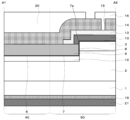
- FIG. 3 is a schematic cross-sectional view showing a schematic configuration of the semiconductor device according to the first embodiment, showing a cross section taken along line A1-A2 of FIG.
- the semiconductor device is provided with a drift layer 2, a well region 3, an impurity region 4, a contact region 5, a gate trench 6, a gate insulating film 8 and a first gate electrode 9 on the front side of a semiconductor substrate 1. Furthermore, a termination trench 7, a field insulating film 10, a first electric field relaxation region 11, a second electric field relaxation region 12 and a second gate electrode 13 are provided. Further, as shown in FIG. 2, the semiconductor device is provided with a rear surface ohmic electrode 19 and a rear surface electrode 21 on the back side of the semiconductor substrate 1 .
- the terminal trench upper edge portion 7a farther from the gate trench 6 is covered with the field insulating film 10 thicker than the gate insulating film 8.
- a second gate electrode 13 is formed on the field insulating film 10 from above the first gate electrode 9 .
- Drift layer 2 is provided on semiconductor substrate 1 made of n-type silicon carbide and made of n-type silicon carbide.
- the n-type impurity of the drift layer 2 may be nitrogen or phosphorus, and the impurity concentration of the drift layer 2 may be approximately 1 ⁇ 10 14 cm ⁇ 3 or more and 1 ⁇ 10 17 cm ⁇ 3 or less.
- the thickness of the drift layer 2 may be about 5 ⁇ m or more and 200 ⁇ m or less.
- Well region 3 is a p-type region provided in the surface layer of drift layer 2 and is made of silicon carbide.
- the p-type impurity of the well region 3 may be aluminum, boron or gallium, and the impurity concentration of the well region 3 may be approximately 1 ⁇ 10 15 cm ⁇ 3 or more and 1 ⁇ 10 20 cm ⁇ 3 or less.
- the impurity concentration of the well region 3 may or may not be constant in the depth direction.
- the thickness of the well region 3 may be about 0.3 ⁇ m or more and 3 ⁇ m or less.
- Impurity region 4 is an n-type region provided in the surface layer of well region 3 and is made of silicon carbide.
- impurity region 4 is, in other words, a source region.
- the n-type impurity of the impurity region 4 may be nitrogen or phosphorus, and the impurity concentration of the impurity region 4 may be approximately 1 ⁇ 10 18 cm ⁇ 3 or more and 1 ⁇ 10 21 cm ⁇ 3 or less.
- the thickness of impurity region 4 may be equal to or less than the thickness of well region 3 .
- the contact region 5 is a p-type region provided on the surface layer of the well region 3 and is made of silicon carbide. Contact region 5 is connected to impurity region 4 and surface ohmic electrode 18, which will be described later. When the contact region 5 is formed, a path connecting from the impurity region 4 to the surface ohmic electrode 18 via the contact region 5 is formed. .
- the p-type impurity of the contact region 5 may be aluminum, boron or gallium, and the impurity concentration of the contact region 5 may be about 1 ⁇ 10 18 cm ⁇ 3 or more and 1 ⁇ 10 22 cm ⁇ 3 or less. .
- the thickness of the contact region 5 should be equal to or less than the thickness of the well region 3 . Although an example in which the semiconductor device is provided with the contact region 5 is shown here, it may not be provided.
- the gate trench 6 is a groove extending from the surface of the impurity region 4 through the well region 3 to the drift layer 2 .
- the gate trenches 6 are provided in stripes, that is, in parallel in the active region 40, as shown in FIG.
- the channel mobility is high (1-100) when the semiconductor device of the present embodiment is a trench gate type MOSFET using silicon carbide for the semiconductor substrate 1 and the drift layer 2.
- a surface such as a surface can be used as a channel, and the characteristics of the semiconductor device can be improved.
- the gate trench 6 extends in the direction from the active region 40 toward the termination region 50 . Hereinafter, this extending direction may be the extending direction of the gate trench 6 .
- the width of the gate trench 6 refers to the width in the left-right direction of the cross section on the front side in FIG.
- the width of the gate trench 6 refers to the width of the widest portion of the tapered shape.
- the depth of the gate trench 6 may be about 1 ⁇ m or more and 6 ⁇ m or less.
- the termination trench 7 is a groove that is connected to the gate trench 6 in a plan view and has a width in the extending direction of the gate trench 6 that is wider than the width of the gate trench 6 .
- the termination trench 7 can be provided by extending the gate trench 6 in plan view.
- the depth of the termination trench 7 may or may not be the same as the depth of the gate trench 6 .
- the width of the terminal trench 7 in the extending direction of the gate trench 6 may be three times or less the width of the gate trench 6, and may be, for example, more than 1 ⁇ m and 30 ⁇ m or less.
- the width of the termination trench 7 is selected in this manner, the top corner portion 7a of the termination trench farther from the gate trench 6 can be easily covered with the field insulating film 10, which will be described later, and the gate lead-out portion 70 can be easily formed. That is, the first gate electrode 9 and the second gate electrode 13 formed in the termination trench 7, which will be described later, can be connected without using the process of opening the field insulating film 10 with high precision. In addition, it is possible to prevent the first gate electrode 9 from disappearing and breaking in the etch-back process of the first gate electrode 9, which will be described later.
- the termination trench upper corner 7a is located at the boundary between the inner side and the outer side of the termination trench 7, one point of the corner of the termination trench 7, and the gate near the corner. It includes a region where an insulating film 8 can be formed. That is, the termination trench upper corner portion 7a includes a part inside and a part outside the termination trench 7, in other words, includes the vicinity of the termination trench upper corner portion 7a.
- the gate insulating film 8 is formed in contact with the inner surfaces of the gate trench 6 and the termination trench 7 and is made of silicon dioxide. As shown in FIG. 2, the gate insulating film 8 is formed inside the gate trench 6 and the termination trench 7 at or below the gate trench upper corner 6a and the termination trench upper corner 7a. formed. The thickness of the gate insulating film 8 can be about 10 nm or more and 100 nm or less. 2 or 3, the gate insulating film 8 may be formed outside the gate trench 6 or the termination trench 7, for example, on the well region 3 of the termination region 50 or on the impurity region 4. good. When the gate insulating film 8 is formed on the well region 3 of the termination region 50, the gate insulating film 8 covers the termination trench upper end corner 7a.
- the first gate electrode 9 is formed inside the gate trench 6 and the terminal trench 7 via the gate insulating film 8, and is made of a conductive material such as polysilicon. As shown in FIG. 2, the upper end of the first gate electrode 9 is located inside the gate trench 6 and the termination trench 7 at or nearer than the gate trench top corner portion 6a and the termination trench top corner portion 7a, respectively. It may also be formed in a low position, ie downward.
- the gate trench upper corner portion 6a and the termination trench upper corner portion 7a do not overlap in the operating state of the semiconductor device.
- the electric field applied to the gate insulating film 8 formed in the vicinity of the portion 7a can be relaxed, and the breakdown of the gate insulating film 8 can be prevented.
- the field insulating film 10 is in contact with the first gate electrode 9 formed in the termination trench 7 , covers the upper end corner portion 7 a of the termination trench 7 farther from the gate trench 6 in the extending direction of the gate trench 6 , and covers the top corner portion 7 a of the termination trench 7 . Formed from the inside to the outside. In other words, the field insulating film 10 is formed continuously from the upper surface of the first gate electrode 9 to the outer peripheral surface of the termination trench 7 while covering the termination trench upper corner portion 7a.
- FIG. 3 shows an example in which the field insulating film 10 is formed on the first gate electrode 9 in the termination region 50 and on the gate insulating film 8 overlapping the termination trench upper end corner 7 a and the well region 3 . ing.
- the thickness of the field insulating film 10 may be greater than the thickness of the gate insulating film 8, and may be, for example, 0.1 ⁇ m or more and 5.0 ⁇ m or less.
- the field insulating film 10 thicker than the gate insulating film 8 is configured to cover the top of the termination trench upper corner 7a farther from the gate trench 6, the termination trench upper corner 7a is covered only with the gate insulating film 8.
- the electric field applied to the gate insulating film 8 formed in the vicinity of the upper end corner portion 7a of the termination trench can be relaxed, and the breakdown of the gate insulating film 8 can be suppressed.
- the thickness of the field insulating film 10 is set to be at least twice the thickness of the gate insulating film 8, breakdown of the gate insulating film 8 can be further suppressed.
- the field insulating film 10 can be made of an insulating material such as silicon dioxide.
- First electric field relaxation region 11 is a p-type region provided below the bottom surface of gate trench 6 and is made of silicon carbide.
- the first electric field relaxation region 11 has a conductivity type opposite to the conductivity type of the drift layer 2, and relaxes the electric field applied to the gate insulating film 8 formed on the bottom surface of the gate trench 6 in the operating state of the semiconductor device, Breakage of the gate insulating film 8 can be prevented.
- the depth of the first electric field relaxation region 11 can be about 0.1 ⁇ m or more and 2.0 ⁇ m or less downward from the bottom surface of the gate trench 6 .
- the first electric field relaxation region 11 may be in contact with the bottom surface of the gate trench 6 .
- the p-type impurity of the first electric field relaxation region 11 may be aluminum, boron or gallium, and the impurity concentration of the first electric field relaxation region 11 is 1 ⁇ 10 15 cm ⁇ 3 or more and 1 ⁇ 10 19 cm ⁇ 3 or less. It should be to some extent.
- Second electric field relaxation region 12 is a p-type region provided below the bottom surface of termination trench 7 and is made of silicon carbide.
- the second electric field relaxation region 12 has a conductivity type opposite to the conductivity type of the drift layer 2, and relaxes the electric field applied to the gate insulating film 8 formed on the bottom surface of the termination trench 7 in the operating state of the semiconductor device, Breakage of the gate insulating film 8 can be prevented.
- the depth of the second electric field relaxation region 12 can be about 0.1 ⁇ m or more and 2.0 ⁇ m or less downward from the bottom surface of the termination trench 7 .
- the second electric field relaxation region 12 may be in contact with the bottom surface of the termination trench 7 .
- the p-type impurity of the second electric field relaxation region 12 may be aluminum, boron or gallium, and the impurity concentration of the first electric field relaxation region 11 is 1 ⁇ 10 15 cm ⁇ 3 or more and 1 ⁇ 10 19 cm ⁇ 3 or less. It should be to some extent.
- the second gate electrode 13 is in contact with the top of the field insulating film 10 and the top of the first gate electrode 9 formed in the termination trench 7 , and extends from the inside to the outside of the termination trench 7 in the extension direction of the gate trench 6 . It rides on the insulating film 10 . That is, the second gate electrode 13 is continuously formed from the upper surface of the first gate electrode 9 to the upper surface of the field insulating film 10 beyond the step at the end of the field insulating film 10 . It covers the edge of the upper field insulating film 10 .
- the second gate electrode 13 can be made of the same material as the first gate electrode 9, such as polysilicon, or can be made of a material different from that of the first gate electrode 9, such as a metal material such as aluminum. If the second gate electrode 13 is made of a material different from that of the first gate electrode 9, the second gate electrode 13 can be easily manufactured.
- the second gate electrode 13 is a wiring that connects the first gate electrode 9 formed in the termination trench 7 to the gate pad 16, as shown in FIG.
- Gate pad 16 is formed on second gate electrode 13 outside termination trench 7 and is connected to second gate electrode 13 through gate contact hole 15 provided in interlayer insulating film 14 made of silicon dioxide. be done.
- Gate pad 16 is also formed on interlayer insulating film 14 .
- the surface electrode 20 is separated from the gate pad 16 and formed on the interlayer insulating film 14 .
- the surface electrode 20 is made of a metal material such as aluminum.
- the back surface ohmic electrode 19 is formed on the back surface of the semiconductor substrate 1 and is composed of a reaction product between a metal film containing nickel as a main component and the semiconductor substrate 1, such as nickel silicide.
- the backside electrode 21 is formed in contact with the backside ohmic electrode 19 and is made of titanium, nickel, silver, gold, aluminum, or the like.
- the semiconductor device according to the present embodiment is configured as described above.
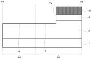
- FIGS. 4 to 8 are explanatory diagrams of each manufacturing stage of the semiconductor device, and correspond to the cross section taken along line A1-A2 in FIG. First, the manufacturing method of the semiconductor device up to the state of FIG. 4 will be described without using the drawings.
- a semiconductor substrate 1 made of n-type silicon carbide having a 4H polytype is prepared, and an n-type drift layer 2 is formed on the front side of the semiconductor substrate 1 by chemical vapor deposition (CVD) or the like. Grow epitaxially. Subsequently, using a resist mask formed on the drift layer 2 by photolithography, ions of aluminum, boron, or gallium are implanted to form a p-type well region 3 in the surface layer of the drift layer 2 .
- the well region 3 may be provided by epitaxial growth.
- n-type impurity region 4 in other words, a source region
- aluminum, boron or gallium is ion-implanted to provide p-type contact region 5 in the surface layer of well region 3 .
- the heating temperature of the semiconductor substrate 1 in the ion implantation should be 150° C. or higher. When the heating temperature is 150° C. or higher, the electrical resistance of the contact region 5 can be lowered, and the resistance loss in the operating state of the semiconductor device can be reduced.
- a silicon dioxide film having a thickness of about 1 ⁇ m to 2 ⁇ m is formed on the well region 3, the impurity region 4 and the contact region 5, and a gate trench 6 and a termination trench 7 are formed by reactive ion etching (RIE).
- RIE reactive ion etching
- An etching mask 22 having an opening at a position corresponding to is formed.
- a gate trench 6 and a termination trench 7 are formed by RIE. In this way, the state shown in FIG. 4 is obtained.
- a first electric field relaxation region 11 and a second electric field relaxation region 12 are provided below the gate trench 6 and the termination trench 7, respectively, and a gate insulating film 8 is provided inside the gate trench 6 and the termination trench 7.
- a first gate electrode 9 is formed.
- annealing is performed to activate the implanted impurity ions.
- Annealing is performed in an atmosphere of an inert gas such as argon or in vacuum at a temperature of about 1500° C. to 1900° C. for about 30 seconds to 1 hour.
- a carbon film may be formed on the silicon carbide before the annealing treatment in order to prevent deterioration of the silicon carbide due to high-temperature heating, that is, surface roughening.
- the gate insulating film 8 is formed on the surface of the drift layer 2 including the inside of the gate trench 6 and the termination trench 7 and the surface of the well region 3 of the termination region 50 by thermal oxidation, CVD, or the like.
- Polysilicon that will be the first gate electrode 9 is formed by the CVD method or the like. Further, the polysilicon is etched by an etch-back process to form the first gate electrode 9 inside the gate trench 6 and the termination trench 7 below the position of the gate trench upper corner 6a and the termination trench upper corner 7a, respectively. do. In this way, the state shown in FIG. 5 is obtained.
- FIG. 6 shows a state in which the field insulating film 10 covers the top corner portion 7a of the termination trench farther from the gate trench 6 .
- an insulating film such as silicon dioxide, which becomes the field insulating film 10 is formed by CVD or the like, and a resist mask is formed on this insulating film by photolithography. Then, this insulating film is etched and opened to form a field insulating film 10, and the resist mask is removed. In this way, the state shown in FIG. 6 is obtained.
- the field insulating film 10 may be formed by patterning an insulating film by RIE, may be formed by patterning by wet etching such as hydrofluoric acid, or may be formed by combining these. good.
- the manufacturing process can be facilitated or made more precise than when the field insulating film 10 is formed by opening the insulating film with high precision by dry etching.
- Field insulating film 10 can be formed so as to protect upper end corner 7a of termination trench.
- LOCS Local Oxidation of Silicon
- FIG. 7 shows a state in which the second gate electrode 13 is formed on the first gate electrode 9 and the field insulating film 10 covering the top corner portion 7a of the termination trench.
- a conductive material such as polysilicon that will be the second gate electrode 13 is formed by CVD or the like, and a resist mask is formed on the polysilicon by photolithography. Subsequently, the polysilicon is etched to form the second gate electrode 13, and the resist mask is removed. In this way, the state shown in FIG. 7 is obtained.
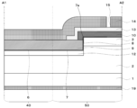
- FIG. 8 shows the state in which the interlayer insulating film 14 provided with the gate contact hole 15 and the rear surface ohmic electrode 19 are formed.
- an interlayer insulating film 14 is formed on the first gate electrode 9 and the second gate electrode 13 by low pressure CVD or the like, and a resist mask is formed on the interlayer insulating film 14 by photolithography.
- the interlayer insulating film 14 is etched to form a source contact hole 17 (to be described later), a metal film is formed so as to be in contact with the impurity region 4 and the contact region 5, and an annealing process is performed.
- a surface ohmic electrode 18, which will be described later, is formed.
- the metal film on the interlayer insulating film 14 is removed by etching, and the resist mask is removed.
- a metal film is formed on the back surface of the semiconductor substrate 1 and annealed to form the back surface ohmic electrode 19 .
- the heating temperature for each annealing treatment may be about 600° C. or higher and 1100° C. or lower.
- a resist mask is formed on the interlayer insulating film 14 by photolithography. Subsequently, the interlayer insulating film 14 positioned outside the termination trench 7 is etched to form a gate contact hole 15 reaching the second gate electrode 13, and the resist mask is removed. In this way, the state shown in FIG. 8 is obtained.
- a metal film such as aluminum is formed on the interlayer insulating film 14 and inside the gate contact hole 15 by sputtering or vapor deposition, and a resist mask is formed on the metal film by photolithography. Subsequently, the metal film is separated by etching, the gate pad 16 and the surface electrode 20 are formed, and the resist mask is removed. Finally, a backside electrode 21 is formed on the backside ohmic electrode 19 by sputtering, vapor deposition, or the like.
- the semiconductor device shown in FIG. 3 is manufactured.
- an electric field is generated in the gate insulating film 8 near the gate trench upper corner 6a and the termination trench upper corner 7a.
- the first gate electrode 9 is formed at the position between the gate trench top corner 6a and the termination trench top corner 7a or at a position lower than that position, and the field insulating film 10 is formed at the top of the termination trench farther from the gate trench 6. It is formed to cover the upper side of the corner portion 7a, suppresses the electric field generated in the gate insulating film 8 in the vicinity of the gate trench upper end corner portion 6a and the termination trench upper end corner portion 7a, and prevents the breakdown of the gate insulating film 8. be.
- the second gate electrode 13 is formed above the upper end corner portion 7a of the terminal trench farther from the gate trench 6 via the field insulating film 10 thicker than the gate insulating film 8. An electric field to the insulating film 8 is suppressed, and breakdown of the gate insulating film 8 is prevented.
- the depletion layer extends downward from the first electric field relaxation region 11 and the second electric field relaxation region 12, that is, to the drift layer 2 as well. Further, breakdown of the gate insulating film 8 at the bottom surface or the bottom corner portion of the gate trench 6 and the termination trench 7 due to the electric field generated by the high voltage applied between the front surface electrode 20 and the rear surface electrode 21 is suppressed. .
- the semiconductor device changes from the off state to the on state, the voltage applied between the front surface electrode 20 and the rear surface electrode 21 is reduced, and the depletion layer spreading to the drift layer 2 shrinks.
- the semiconductor device according to the present embodiment alternately repeats the ON state and the OFF state to operate.
- the semiconductor device By configuring the semiconductor device in this manner, it is possible to obtain a semiconductor device in which the gate insulating film 8 formed at the upper end corner portion 7a of the termination trench farther from the gate trench 6 in the gate lead-out portion 70 is prevented from being broken. .
- the field insulating film 10 can be easily manufactured, or the field insulating film 10 can be formed so as to protect the upper end corner 7a of the termination trench with high accuracy. can be formed.
- the formation time can be shortened, and the manufacturing cost can be reduced.
- the field insulating film 10 can be patterned by wet etching, overetching of the first gate electrode 9 is suppressed when the field insulating film 10 is etched.
- the second gate electrode 13 may be formed so as to surround the gate trench 6 in plan view.
- the termination trench 7 or the field insulating film 10 may be formed so as to completely surround the gate trench 6 in a plan view, or may be formed so as to have an intermittent portion.
- the termination trench 7 is formed on the side of the gate pad 16 in plan view, but it does not have to be formed on the side.
- the termination trench 7 may continuously surround the gate trench 6 in plan view without discontinuing the gate trench 6 at the position corresponding to the gate pad 16 in FIG.
- the gate pad 16 may be connected to the second gate electrode 13 via a gate contact hole 15 provided in the interlayer insulating film 14 (not shown) on the second gate electrode 13 outside the termination trench 7. .
- the gate wiring may be extended along the second gate electrode 13 or the interlayer insulating film 14 and connected to the gate pad 16 . In this case, the gate wiring can be easily formed by depositing and etching a metal film at the same time when the gate pad 16 is formed.
- the termination region 50 may be provided with a channel stop region 23 for suppressing extension of the depletion layer to the edge of the semiconductor device.
- Channel stop region 23 is an n-type region provided on the outer peripheral side of termination trench 7 and is made of silicon carbide.
- the n-type impurity of the channel stop region 23 may be nitrogen or phosphorus, and the impurity concentration of the channel stop region 23 may be approximately 1 ⁇ 10 18 cm ⁇ 3 or more and 1 ⁇ 10 21 cm ⁇ 3 or less.
- the thickness of channel stop region 23 may be the same as or different from that of impurity region 4 .
- the channel stop region 23 may be provided by ion implantation, and may be formed simultaneously with the impurity region 4 using a resist mask for providing the impurity region 4, or may be formed before or after the impurity region 4 is formed. You may
- an outer electric field relaxation region 24 such as an FLR (Field Limiting Ring) may be provided continuously or intermittently in the termination region 50 surrounding the active region 40 .
- an FLR Field Limiting Ring
- ions of aluminum, boron, or the like are implanted from the surface of the drift layer 2 to a depth of about 0.2 to 3 ⁇ m not exceeding the drift layer 2 to form a continuous p-type peripheral electric field relaxation region 24 surrounding the active region 40 .
- the p-type impurity concentration of the peripheral electric field relaxation region 24 should exceed the impurity concentration of the drift layer 2 and should be 1 ⁇ 10 15 cm ⁇ 3 or more and 1 ⁇ 10 19 cm ⁇ 3 or less.
- the well region 3 and the impurity region 4 are formed by ion-implanting an n-type impurity into the surface layer of the well region 3 to form the impurity region 4, and then forming a resist mask thereon by photolithography.
- the well region 3 may be formed by ion-implanting a p-type impurity at a position other than the above.
- the thickness of the etching mask 22 and the RIE process were adjusted so that the etching mask 22 remained after the gate trench 6 and the termination trench 7 were formed.
- the first electric field relaxation region 11 and the second electric field relaxation region 12 may be formed by ion implantation using a mask.
- the first electric field relaxation region 11 may be formed at the same time as the second electric field relaxation region 12, or may be formed before or after the first electric field relaxation region 11 is formed. Furthermore, a p-type impurity is ion-implanted obliquely into the opening of the gate trench 6 to form a p-type semiconductor layer in the drift layer 2 in contact with the side surface of the gate trench 6, forming a first electric field relaxation region 11.
- the well region 3 may be electrically connected through the semiconductor layer.
- the conductivity type of the semiconductor substrate 1 may be p-type, and the thickness of the semiconductor substrate 1 may be reduced by polishing.
- the second gate electrode 13 does not branch at the connection portion between the first gate electrode 9 and the second gate electrode 13.
- the second gate electrode 13 is An example having a plurality of branched, ie, separated, lead-out portions will be described. Other configurations are the same as those of the first embodiment.
- FIG. 10 is a schematic diagram showing the schematic configuration of the semiconductor device according to the present embodiment, and corresponds to a perspective view of the cross section and upper surface of the partial region 60 in FIG.
- the second gate electrode 13 has a second gate electrode lead-out portion 13a and a second gate electrode peripheral portion 13b.
- a lead portion 13 a is connected to the first gate electrode 9 .
- a plurality of second gate electrode extension portions 13a are formed apart from each other, are in contact with the top of the field insulating film 10 and the top of the first gate electrode 9 formed in the termination trench 7, and terminate in the extending direction of the gate trench 6. It runs over the field insulating film 10 from the inside to the outside of the trench 7 . That is, the second gate electrode lead-out portion 13a is continuously formed from the upper surface of the first gate electrode 9 to the upper surface of the field insulating film 10 over the step at the end of the field insulating film 10, forming a termination trench. The edge of the field insulating film 10 on 7 is covered. Further, as shown in FIG. 10, the end portion of the field insulating film 10 is exposed in the regions where the plurality of second gate electrode lead-out portions 13a are separated from each other.
- the second gate electrode peripheral portion 13b is formed on the field insulating film 10 and is in contact with the second gate electrode lead-out portion 13a.
- the second gate electrode peripheral portion 13b is a wiring that connects the first gate electrode 9 formed in the termination trench 7 to the gate pad 16 via the second gate electrode lead-out portion 13a.
- the second gate electrode outer peripheral portion 13 b is connected to a gate pad 16 via a gate contact hole 15 reaching the second gate electrode 13 provided in the interlayer insulating film 14 outside the termination trench 7 .
- Gate pad 16 is also formed on interlayer insulating film 14 .
- the gate contact hole 15 may be provided in the interlayer insulating film above the second gate electrode lead-out portion 13a.
- the termination trench 7 is divided as shown in FIG. can be formed by That is, the termination trenches 7 can be intermittently provided surrounding the active region 40 in which the gate trenches 6 are formed. In this way, when the first gate electrode 9 is formed inside the termination trench 7 by etchback, the etchback can proceed in the same manner as the gate trench 6 connected to the divided termination trench 7. loss of the first gate electrode 9 due to
- Embodiment 3 In the first embodiment, an example in which the gate trenches 6 are provided in a stripe pattern when viewed from above is shown, but in the present embodiment, an example in which the gate trenches 6 are provided in a grid pattern when viewed from above will be described. Other configurations are the same as those of the first embodiment.
- FIG. 12 is a schematic plan view showing the schematic configuration of the semiconductor device according to the present embodiment.
- the gate trenches 6 are provided in a grid pattern in the active region 40 , and the first gate electrodes 9 are formed inside the gate trenches 6 .
- the plurality of gate trenches 6 are provided in an orthogonal grid pattern throughout the active region 40, but may have non-orthogonal portions, that is, may be provided in a zigzag pattern.
- FIG. 13 is a schematic diagram showing a schematic configuration of the semiconductor device according to the present embodiment, showing a cross section taken along line B1-B2 in FIG. Even when the gate trenches 6 are provided in a lattice pattern, it is preferable that the depth of the gate trenches 6 is the same as or approximately the same as the depth of the termination trenches 7, as shown in FIG.
- FIG. 13 shows an example in which the source contact hole 17 is provided in the interlayer insulating film 14 in the active region 40, and the contact region 5 and the surface ohmic electrode 18 are formed on and in contact with the contact region 5. , the contact region 5 and the surface ohmic electrode 18 may not be formed.
- the surface ohmic electrode 18 is composed of a reaction product of a metal film containing nickel as a main component and the semiconductor substrate 1, such as nickel silicide.
- the same effect as in the first embodiment can be obtained.
- the gate trenches 6 are arranged in a grid pattern, power loss due to the resistance of the first gate electrode 9 in the switching operation of the semiconductor device can be suppressed as compared with the arrangement in which the gate trenches 6 are arranged in stripes.
- each embodiment may have one or more than one component of the invention.
- an inventive component may be a conceptual unit consisting of multiple structures and corresponding to a portion of a structure.
Landscapes
- Electrodes Of Semiconductors (AREA)
Priority Applications (5)
| Application Number | Priority Date | Filing Date | Title |
|---|---|---|---|
| DE112022006775.6T DE112022006775T5 (de) | 2022-03-03 | 2022-03-03 | Halbleitereinrichtung und Herstellungsverfahren für eine Halbleitereinrichtung |
| JP2023524727A JP7338813B1 (ja) | 2022-03-03 | 2022-03-03 | 半導体装置および半導体装置の製造方法 |
| US18/840,521 US20250185285A1 (en) | 2022-03-03 | 2022-03-03 | Semiconductor device and manufacturing method of semiconductor device |
| CN202280092813.0A CN118786531A (zh) | 2022-03-03 | 2022-03-03 | 半导体装置以及半导体装置的制造方法 |
| PCT/JP2022/009146 WO2023166666A1 (ja) | 2022-03-03 | 2022-03-03 | 半導体装置および半導体装置の製造方法 |
Applications Claiming Priority (1)
| Application Number | Priority Date | Filing Date | Title |
|---|---|---|---|
| PCT/JP2022/009146 WO2023166666A1 (ja) | 2022-03-03 | 2022-03-03 | 半導体装置および半導体装置の製造方法 |
Publications (1)
| Publication Number | Publication Date |
|---|---|
| WO2023166666A1 true WO2023166666A1 (ja) | 2023-09-07 |
Family
ID=87882198
Family Applications (1)
| Application Number | Title | Priority Date | Filing Date |
|---|---|---|---|
| PCT/JP2022/009146 Ceased WO2023166666A1 (ja) | 2022-03-03 | 2022-03-03 | 半導体装置および半導体装置の製造方法 |
Country Status (5)
| Country | Link |
|---|---|
| US (1) | US20250185285A1 (https=) |
| JP (1) | JP7338813B1 (https=) |
| CN (1) | CN118786531A (https=) |
| DE (1) | DE112022006775T5 (https=) |
| WO (1) | WO2023166666A1 (https=) |
Cited By (1)
| Publication number | Priority date | Publication date | Assignee | Title |
|---|---|---|---|---|
| WO2025143233A1 (ja) * | 2023-12-27 | 2025-07-03 | ローム株式会社 | 半導体装置 |
Families Citing this family (2)
| Publication number | Priority date | Publication date | Assignee | Title |
|---|---|---|---|---|
| US20250107124A1 (en) * | 2023-09-27 | 2025-03-27 | Wolfspeed, Inc. | Power Semiconductor Device Having Shaped Trench Ends |
| WO2025134220A1 (ja) * | 2023-12-19 | 2025-06-26 | 三菱電機株式会社 | 半導体装置、および、半導体装置の製造方法 |
Citations (3)
| Publication number | Priority date | Publication date | Assignee | Title |
|---|---|---|---|---|
| JP2001177093A (ja) * | 1999-12-20 | 2001-06-29 | Toyota Central Res & Dev Lab Inc | 絶縁ゲート型半導体装置 |
| JP2009505433A (ja) * | 2005-08-17 | 2009-02-05 | インターナショナル レクティファイアー コーポレイション | ゲートトレンチで相互接続されたパワー半導体デバイス |
| WO2016047438A1 (ja) * | 2014-09-26 | 2016-03-31 | 三菱電機株式会社 | 半導体装置 |
Family Cites Families (4)
| Publication number | Priority date | Publication date | Assignee | Title |
|---|---|---|---|---|
| US6861701B2 (en) | 2003-03-05 | 2005-03-01 | Advanced Analogic Technologies, Inc. | Trench power MOSFET with planarized gate bus |
| US7449354B2 (en) * | 2006-01-05 | 2008-11-11 | Fairchild Semiconductor Corporation | Trench-gated FET for power device with active gate trenches and gate runner trench utilizing one-mask etch |
| DE112017007186B4 (de) * | 2017-03-07 | 2024-06-27 | Mitsubishi Electric Corporation | Halbleitereinheit und leistungswandler |
| JP7201336B2 (ja) * | 2017-05-17 | 2023-01-10 | ローム株式会社 | 半導体装置 |
-
2022
- 2022-03-03 WO PCT/JP2022/009146 patent/WO2023166666A1/ja not_active Ceased
- 2022-03-03 US US18/840,521 patent/US20250185285A1/en active Pending
- 2022-03-03 JP JP2023524727A patent/JP7338813B1/ja active Active
- 2022-03-03 DE DE112022006775.6T patent/DE112022006775T5/de active Pending
- 2022-03-03 CN CN202280092813.0A patent/CN118786531A/zh active Pending
Patent Citations (3)
| Publication number | Priority date | Publication date | Assignee | Title |
|---|---|---|---|---|
| JP2001177093A (ja) * | 1999-12-20 | 2001-06-29 | Toyota Central Res & Dev Lab Inc | 絶縁ゲート型半導体装置 |
| JP2009505433A (ja) * | 2005-08-17 | 2009-02-05 | インターナショナル レクティファイアー コーポレイション | ゲートトレンチで相互接続されたパワー半導体デバイス |
| WO2016047438A1 (ja) * | 2014-09-26 | 2016-03-31 | 三菱電機株式会社 | 半導体装置 |
Cited By (1)
| Publication number | Priority date | Publication date | Assignee | Title |
|---|---|---|---|---|
| WO2025143233A1 (ja) * | 2023-12-27 | 2025-07-03 | ローム株式会社 | 半導体装置 |
Also Published As
| Publication number | Publication date |
|---|---|
| DE112022006775T5 (de) | 2025-01-16 |
| CN118786531A (zh) | 2024-10-15 |
| JPWO2023166666A1 (https=) | 2023-09-07 |
| US20250185285A1 (en) | 2025-06-05 |
| JP7338813B1 (ja) | 2023-09-05 |
Similar Documents
| Publication | Publication Date | Title |
|---|---|---|
| JP7786512B2 (ja) | 半導体装置 | |
| CN101764160B (zh) | 半导体装置 | |
| TWI702722B (zh) | 半導體裝置及半導體裝置之製造方法 | |
| JP6617657B2 (ja) | 炭化ケイ素半導体装置および炭化ケイ素半導体装置の製造方法 | |
| JP6109444B1 (ja) | 半導体装置 | |
| JP7338813B1 (ja) | 半導体装置および半導体装置の製造方法 | |
| JP7643621B2 (ja) | 半導体装置 | |
| CN108074818B (zh) | 半导体器件的制造方法 | |
| JP2019003967A (ja) | 半導体装置および半導体装置の製造方法 | |
| JP2022007788A (ja) | 半導体装置 | |
| JP2017092355A (ja) | 半導体装置および半導体装置の製造方法 | |
| US10439027B2 (en) | Silicon carbide semiconductor device and method for manufacturing the same | |
| JP2018116986A (ja) | 半導体装置および半導体装置の製造方法 | |
| JP6648852B1 (ja) | 炭化珪素半導体装置および炭化珪素半導体装置の製造方法 | |
| JP2008078174A (ja) | トレンチゲート型炭化珪素半導体装置 | |
| WO2015111177A1 (ja) | 半導体装置,パワーモジュール,電力変換装置,および鉄道車両 | |
| JP7851428B2 (ja) | 半導体装置、および、半導体装置の製造方法 | |
| CN116325175B (zh) | 半导体装置以及半导体装置的制造方法 | |
| KR101965550B1 (ko) | 반도체 장치 | |
| JP7752780B2 (ja) | 半導体装置およびその製造方法 | |
| JP2014241426A (ja) | 半導体装置 | |
| WO2025134220A1 (ja) | 半導体装置、および、半導体装置の製造方法 | |
| JP6102564B2 (ja) | 半導体装置及びその製造方法 | |
| CN120603279A (zh) | 功率器件及其制造方法 | |
| CN113875018A (zh) | 半导体装置以及半导体装置的制造方法 |
Legal Events
| Date | Code | Title | Description |
|---|---|---|---|
| WWE | Wipo information: entry into national phase |
Ref document number: 2023524727 Country of ref document: JP |
|
| 121 | Ep: the epo has been informed by wipo that ep was designated in this application |
Ref document number: 22929811 Country of ref document: EP Kind code of ref document: A1 |
|
| WWE | Wipo information: entry into national phase |
Ref document number: 18840521 Country of ref document: US |
|
| WWE | Wipo information: entry into national phase |
Ref document number: 202280092813.0 Country of ref document: CN |
|
| WWE | Wipo information: entry into national phase |
Ref document number: 112022006775 Country of ref document: DE |
|
| 122 | Ep: pct application non-entry in european phase |
Ref document number: 22929811 Country of ref document: EP Kind code of ref document: A1 |
|
| WWP | Wipo information: published in national office |
Ref document number: 18840521 Country of ref document: US |