WO2023163003A1 - エッチング用組成物およびそれを用いた配線基板の製造方法 - Google Patents
エッチング用組成物およびそれを用いた配線基板の製造方法 Download PDFInfo
- Publication number
- WO2023163003A1 WO2023163003A1 PCT/JP2023/006336 JP2023006336W WO2023163003A1 WO 2023163003 A1 WO2023163003 A1 WO 2023163003A1 JP 2023006336 W JP2023006336 W JP 2023006336W WO 2023163003 A1 WO2023163003 A1 WO 2023163003A1
- Authority
- WO
- WIPO (PCT)
- Prior art keywords
- etching
- copper
- seed layer
- wiring
- etching composition
- Prior art date
- Legal status (The legal status is an assumption and is not a legal conclusion. Google has not performed a legal analysis and makes no representation as to the accuracy of the status listed.)
- Ceased
Links
Images


Classifications
-
- H—ELECTRICITY
- H05—ELECTRIC TECHNIQUES NOT OTHERWISE PROVIDED FOR
- H05K—PRINTED CIRCUITS; CASINGS OR CONSTRUCTIONAL DETAILS OF ELECTRIC APPARATUS; MANUFACTURE OF ASSEMBLAGES OF ELECTRICAL COMPONENTS
- H05K3/00—Apparatus or processes for manufacturing printed circuits
- H05K3/02—Apparatus or processes for manufacturing printed circuits in which the conductive material is applied to the surface of the insulating support and is thereafter removed from such areas of the surface which are not intended for current conducting or shielding
- H05K3/06—Apparatus or processes for manufacturing printed circuits in which the conductive material is applied to the surface of the insulating support and is thereafter removed from such areas of the surface which are not intended for current conducting or shielding the conductive material being removed chemically or electrolytically, e.g. by photo-etch process
- H05K3/067—Etchants
-
- C—CHEMISTRY; METALLURGY
- C09—DYES; PAINTS; POLISHES; NATURAL RESINS; ADHESIVES; COMPOSITIONS NOT OTHERWISE PROVIDED FOR; APPLICATIONS OF MATERIALS NOT OTHERWISE PROVIDED FOR
- C09K—MATERIALS FOR MISCELLANEOUS APPLICATIONS, NOT PROVIDED FOR ELSEWHERE
- C09K13/00—Etching, surface-brightening or pickling compositions
- C09K13/04—Etching, surface-brightening or pickling compositions containing an inorganic acid
- C09K13/06—Etching, surface-brightening or pickling compositions containing an inorganic acid with organic material
-
- C—CHEMISTRY; METALLURGY
- C23—COATING METALLIC MATERIAL; COATING MATERIAL WITH METALLIC MATERIAL; CHEMICAL SURFACE TREATMENT; DIFFUSION TREATMENT OF METALLIC MATERIAL; COATING BY VACUUM EVAPORATION, BY SPUTTERING, BY ION IMPLANTATION OR BY CHEMICAL VAPOUR DEPOSITION, IN GENERAL; INHIBITING CORROSION OF METALLIC MATERIAL OR INCRUSTATION IN GENERAL
- C23F—NON-MECHANICAL REMOVAL OF METALLIC MATERIAL FROM SURFACE; INHIBITING CORROSION OF METALLIC MATERIAL OR INCRUSTATION IN GENERAL; MULTI-STEP PROCESSES FOR SURFACE TREATMENT OF METALLIC MATERIAL INVOLVING AT LEAST ONE PROCESS PROVIDED FOR IN CLASS C23 AND AT LEAST ONE PROCESS COVERED BY SUBCLASS C21D OR C22F OR CLASS C25
- C23F1/00—Etching metallic material by chemical means
- C23F1/10—Etching compositions
- C23F1/14—Aqueous compositions
- C23F1/16—Acidic compositions
- C23F1/18—Acidic compositions for etching copper or alloys thereof
-
- H—ELECTRICITY
- H05—ELECTRIC TECHNIQUES NOT OTHERWISE PROVIDED FOR
- H05K—PRINTED CIRCUITS; CASINGS OR CONSTRUCTIONAL DETAILS OF ELECTRIC APPARATUS; MANUFACTURE OF ASSEMBLAGES OF ELECTRICAL COMPONENTS
- H05K3/00—Apparatus or processes for manufacturing printed circuits
- H05K3/02—Apparatus or processes for manufacturing printed circuits in which the conductive material is applied to the surface of the insulating support and is thereafter removed from such areas of the surface which are not intended for current conducting or shielding
- H05K3/06—Apparatus or processes for manufacturing printed circuits in which the conductive material is applied to the surface of the insulating support and is thereafter removed from such areas of the surface which are not intended for current conducting or shielding the conductive material being removed chemically or electrolytically, e.g. by photo-etch process
-
- H—ELECTRICITY
- H05—ELECTRIC TECHNIQUES NOT OTHERWISE PROVIDED FOR
- H05K—PRINTED CIRCUITS; CASINGS OR CONSTRUCTIONAL DETAILS OF ELECTRIC APPARATUS; MANUFACTURE OF ASSEMBLAGES OF ELECTRICAL COMPONENTS
- H05K3/00—Apparatus or processes for manufacturing printed circuits
- H05K3/10—Apparatus or processes for manufacturing printed circuits in which conductive material is applied to the insulating support in such a manner as to form the desired conductive pattern
- H05K3/108—Apparatus or processes for manufacturing printed circuits in which conductive material is applied to the insulating support in such a manner as to form the desired conductive pattern by semi-additive methods; masks therefor
Definitions
- the present invention relates to an etching composition for selectively etching a copper seed layer from a substrate having a copper wiring pattern and a copper seed layer, and a wiring board manufacturing method using the same.
- SAP Semi-Additive Process
- M-SAP Modified-Semi-Additive Process
- an electroless copper-plated film and, in some cases, an ultra-thin electrolytic copper-plated film are formed on an insulating layer to form a copper seed layer.
- a photoresist is used to form a resist pattern for forming copper wiring on the copper seed layer, and a copper wiring pattern is formed between the resist patterns by electrolytic copper plating.
- the resist pattern is removed and the exposed copper seed layer is removed by chemical etching, so that a fine copper wiring pattern can be formed on the insulating layer.
- M-SAP In M-SAP, first, using an electrolytic copper foil with a carrier foil, the electrolytic copper foil is laminated on the insulating layer, and then this electrolytic copper foil is half-etched as necessary to form an ultra-thin copper thin layer, An electroless copper plating film is formed thereon to form a copper seed layer. Next, a resist pattern for forming copper wiring is formed on the copper seed layer, and a copper wiring pattern is formed between the resist patterns by electrolytic copper plating. Thereafter, the resist pattern is removed and the exposed copper seed layer is removed by chemical etching, thereby forming a fine copper wiring pattern on the insulating layer. Thus, in SAP or M-SAP, it is necessary to remove the copper seed layer after forming the copper wiring pattern.
- Patent Document 1 describes that an etchant containing hydrogen peroxide and sulfuric acid as main components and containing azoles as additives can suppress thinning and skirting of circuit portions when removing a copper seed layer in SAP. .
- An embedded trace substrate (ETS) construction method (hereinafter referred to as "ETS construction method") is also known as a processing method capable of coping with miniaturization of copper wiring (Patent Document 2).
- the ETS method even in the case of the ETS method, after the copper wiring pattern formed on the electrolytic copper foil as the copper seed layer is embedded in the resin, it is necessary to remove the electrolytic copper foil as the copper seed layer by etching. However, depending on the degree of etching (side etching) of the copper wiring along the side wall of the interlayer insulating resin and etching of the upper surface of the copper wiring, the shape of the cross section of the wiring may not be rectangular. Therefore, in the ETS method as well, it is required to selectively etch the electrolytic copper foil as the copper seed layer.
- the term "copper seed layer” refers to a copper thin film that is formed as a base layer when copper wiring is formed on an insulating layer using a plating technique, and the formation method is not particularly limited.
- the copper thin film may be, for example, an electrolytic copper foil, an electrolytic copper-plated film, an electroless copper-plated film, or a combination thereof.
- the present invention relates to the following etching composition and a method for producing a wiring board using the same.
- An etching composition for selectively etching a copper seed layer from a substrate having a copper wiring pattern and a copper seed layer Hydrogen peroxide (A), sulfuric acid (B), azoles or salts thereof (C), glycol ethers (D), halide ions (E), and water (F),
- the content of hydrogen peroxide (A) is 0.1 to 10% by mass based on the total amount of the etching composition
- the content of sulfuric acid (B) is 0.5 to 5% by mass based on the total amount of the etching composition
- the ratio of hydrogen peroxide (A) to sulfuric acid (B) is 2 or more in terms of molar ratio
- the content of halide ions (E) is 0.01 to 3 ppm based on the total amount of the etching composition.
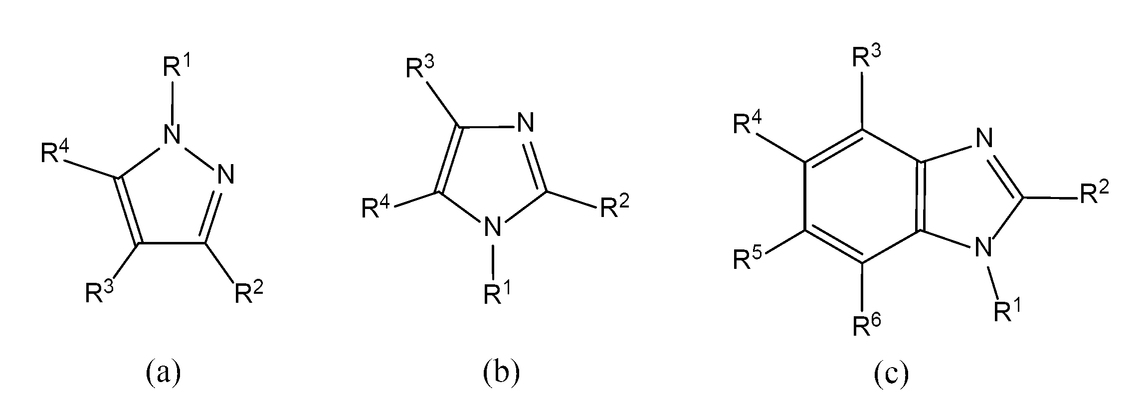
- Etching composition [2] The etching composition according to [1] above, wherein the azole is a five-membered heterocyclic ring having two nitrogen atoms or a heterocyclic compound having a condensed heterocyclic ring thereof. [3] The etching composition according to [2] above, wherein the azole is at least one selected from the group consisting of pyrazoles, imidazoles, and benzimidazoles.
- R 1 , R 2 , R 3 , R 4 , R 5 and R 6 are each independently a hydrogen atom, a C 1 -C 6 alkyl group, a C 6 -C 10 aryl group, a carboxyl group; , a carboxy C 1 -C 6 alkyl group, a nitro group, a hydroxyl group, a C 2 -C 7 carboxylic acid ester, or a halogen atom.
- the etching composition according to [3] above which is one or more selected from the group consisting of the compounds represented by: [5] Azoles are imidazole, 1,2,4,5-tetramethylimidazole, 4-methyl-2-phenylimidazole, benzimidazole, 1-methylbenzimidazole, 2-methylbenzimidazole, 5-methylbenzimidazole , 2,5-dimethylbenzimidazole, 5-nitrobenzimidazole, pyrazole, and 3,5-dimethylpyrazole. [6] The etching composition according to any one of [1] to [5] above, wherein the content of the azole is 0.01 to 0.5% by mass based on the total amount of the etching composition. .
- Glycol ether (D) is at least one selected from the group consisting of ethylene glycol monobutyl ether, diethylene glycol monomethyl ether, diethylene glycol monophenyl ether, and dipropylene glycol monomethyl ether, from [1] to [ 6], the etching composition according to any one of the above items.
- Composition Composition.
- a method of manufacturing a wiring board comprising: [14] The method for producing a wiring board according to [13] above, wherein the copper seed layer is at least one selected from the group consisting of electrolytic copper foil, electrolytic copper-plated film, and electroless copper-plated film.
- a method for producing a wiring board comprising selectively etching a copper seed layer from a substrate having a copper wiring pattern and a copper seed layer using a composition for forming a wiring circuit.
- an etching composition for selectively etching a copper seed layer from a substrate having a copper wiring pattern and a copper seed layer.
- the etching composition of the present invention can be suitably used when manufacturing a wiring board having a wiring circuit composed of a fine copper wiring pattern in the SAP, M-SAP or ETS method.
- the copper seed layer can be selectively removed while suppressing thinning of the copper wiring and maintaining the rectangularity of the cross section of the wiring.
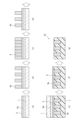
- FIG. 4 is a diagram for explaining a method of manufacturing a wiring substrate in SAP, in which a wiring circuit is formed by selectively etching a copper seed layer from a substrate having a copper wiring pattern and a copper seed layer
- FIG. 10 is a diagram for explaining a method of manufacturing a wiring substrate in which a wiring circuit is formed by selectively etching a copper seed layer from a substrate having a copper wiring pattern and a copper seed layer in M-SAP;
- FIG. 10 is a diagram for explaining a method of manufacturing a wiring substrate in which a wiring circuit is formed by selectively etching a copper seed layer from a substrate having a copper wiring pattern and a copper seed layer in M-SAP;
- FIG. 10 is a diagram for explaining a method of manufacturing a wiring board in which a wiring circuit is formed by selectively etching a copper seed layer from a substrate having a copper wiring pattern and a copper seed layer in the ETS method; It is the figure which showed the specific example of the rectangularity evaluation criteria of the copper wiring after an etching process.
- the etching composition according to the present invention is an etching composition for selectively etching a copper seed layer from a substrate having a copper wiring pattern and a copper seed layer, Hydrogen peroxide (A), sulfuric acid (B), azoles or salts thereof (C), glycol ethers (D), halide ions (E), and water (F),
- the content of hydrogen peroxide (A) is 0.1 to 10% by mass based on the total amount of the etching composition
- the content of sulfuric acid (B) is 0.5 to 5% by mass based on the total amount of the etching composition
- the ratio of hydrogen peroxide (A) to sulfuric acid (B) is 2 or more in terms of molar ratio
- the content of halide ions (E) is 0.01 to 3 ppm based on the total amount of the etching composition.
- hydrogen peroxide (A) (hereinafter sometimes simply referred to as component (A)) is a component that functions as an oxidizing agent for copper. There are no particular restrictions on the component (A), and various grades for industrial and electronic industries can be used. In general, it is preferable to use it as an aqueous solution of hydrogen peroxide in terms of availability and operability.
- the content of component (A) is in the range of 0.1 to 10% by mass, preferably 0.5 to 8% by mass, more preferably 1 to 7.0% by mass, based on the total amount (by mass) of the etching composition. 5% by mass, more preferably in the range of 2 to 7% by mass.
- the copper seed layer can be selectively removed while suppressing thinning of the copper wiring and maintaining the rectangularity of the cross section of the wiring.
- sulfuric acid (B) is a component that acts as an etching agent for copper oxidized by hydrogen peroxide (A).
- the content of component (B) is in the range of 0.5 to 5% by mass, preferably 1 to 5% by mass, more preferably 2 to 5% by mass, based on the total amount (by mass) of the etching composition, More preferably, it is in the range of 2.5 to 5% by mass.
- the copper seed layer can be selectively removed while suppressing thinning of the copper wiring and maintaining the rectangularity of the cross section of the wiring.
- the molar ratio of hydrogen peroxide (A) to sulfuric acid (B) is 2 or more, preferably 2. 0 or more, more preferably 2 to 20, still more preferably 2.0 to 20, still more preferably 3 to 15, still more preferably 3.5 to 10, particularly preferably 3.5 to 8 be.
- the copper seed layer can be selectively removed while suppressing thinning of the copper wiring and maintaining the rectangularity of the cross section of the wiring.
- the azole or its salt (C) (hereinafter sometimes simply referred to as the (C) component) has the function of selectively removing the copper seed layer by adsorbing on the surface of the copper wiring. be able to.
- the azoles are heterocyclic compounds having a five-membered heterocyclic ring having one or more nitrogen atoms or a condensed heterocyclic ring thereof, and the atoms constituting the five-membered heterocyclic ring or condensed heterocyclic ring are alkyl groups, It may have one or more substituents selected from carboxyl groups, carboxyalkyl groups, nitro groups, hydroxyl groups, carboxylic acid esters, halogen atoms and the like.
- Azoles include, for example, pyrazoles, imidazoles, benzimidazoles, triazoles, tetrazoles and the like.
- the azole is preferably a heterocyclic compound having a five-membered heterocyclic ring having two nitrogen atoms or a condensed heterocyclic ring thereof, in that the copper seed layer can be selectively etched with respect to the copper wiring. At least one selected from the group consisting of pyrazoles, imidazoles, and benzimidazoles is particularly preferred.
- the (C) component may be a salt of an azole. Salts of azoles are not particularly limited, but are preferably inorganic acid salts from the viewpoint of economy, and examples thereof include nitrates, sulfates, hydrochlorides, and the like. When the azole salt is a hydrochloride, the chloride ion of the hydrochloride can function as a halide ion (E).
- Pyrazoles are not particularly limited as long as they have a pyrazole skeleton.
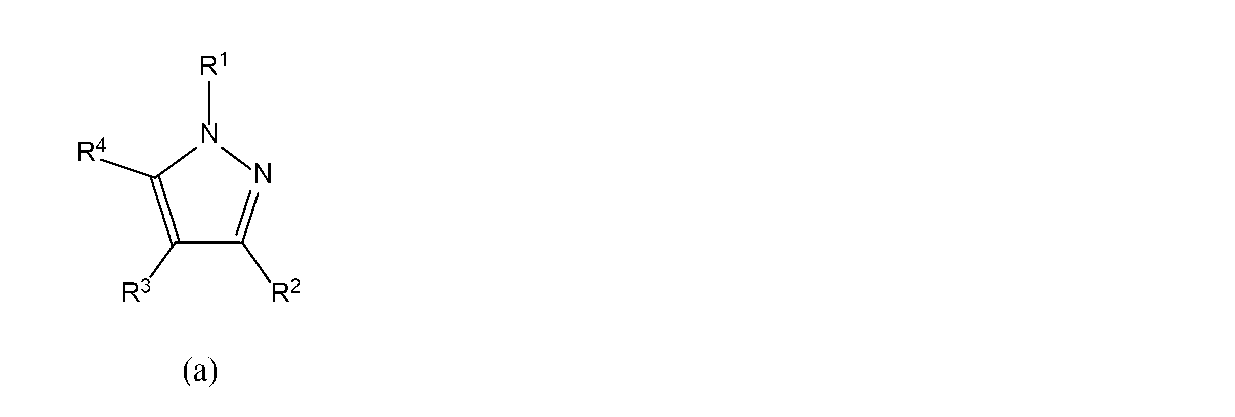
- the following formula: [wherein R 1 , R 2 , R 3 and R 4 are each independently of each other, a hydrogen atom, a C 1 -C 6 alkyl group, a C 6 -C 10 aryl group, a carboxyl group, a carboxy C 1 -C 6 alkyl group, nitro group, hydroxyl group, C 2 to C 7 carboxylic acid ester, or halogen atom. ] It is preferably one or more selected from the group consisting of compounds represented by.
- C 1 -C 6 alkyl group means an alkyl group having 1 to 6 carbon atoms.
- the C 1 -C 6 alkyl groups include methyl, ethyl, propyl, isopropyl, n-butyl, sec-butyl, tert-butyl, pentyl and hexyl groups. Among these, a methyl group and an ethyl group are preferable.
- a “C 6 -C 10 aryl group” means an aryl group having 6 to 10 carbon atoms.
- the C 6 -C 10 aryl groups include phenyl, 1-naphthyl, 2-naphthyl, indenyl, biphenyl, anthryl and phenanthryl groups. Among these, a phenyl group is preferred.
- a “carboxy C 1 -C 6 alkyl group” means an alkyl group having 1 to 6 carbon atoms and having a carboxyl group. Examples of the C 1 -C 6 alkyl group include the same as those described above. Specific examples of the carboxy C 1 -C 6 alkyl group are preferably a carboxymethyl group (--CH 2 --COOH) and a carboxyethyl group (--CH 2 CH 2 --COOH).
- C 2 -C 7 carboxylic acid ester means a group represented by -COOR (R is a C 1 -C 6 alkyl group). Examples of the C 1 -C 6 alkyl group include the same as those described above. Specific examples of C 2 -C 7 carboxylic acid esters are preferably methyl carboxylate and ethyl carboxylate.
- a "halogen atom” may be a fluorine atom, a chlorine atom, a bromine atom, or an iodine atom, and particularly preferably a chlorine atom or a bromine atom.
- R 1 , R 2 , R 3 and R 4 are each independently preferably a hydrogen atom or a C 1 -C 6 alkyl group.
- pyrazoles include pyrazole, 3,5-dimethylpyrazole and the like.
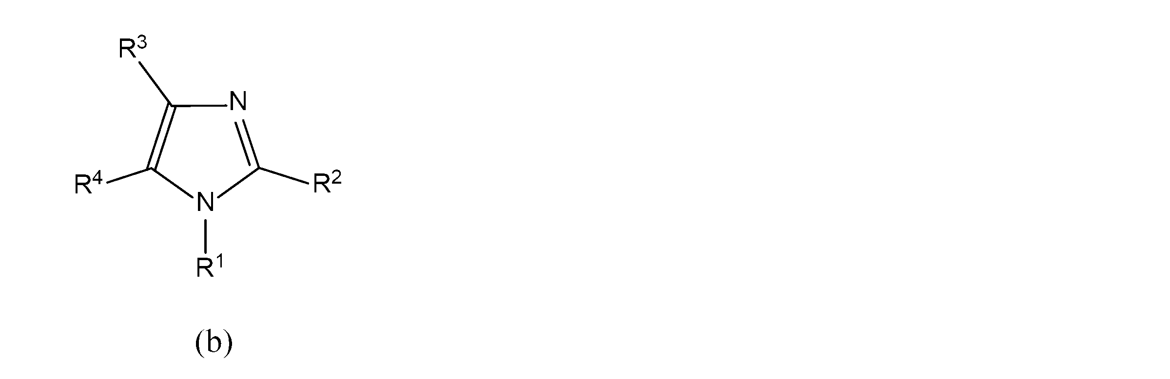
- the imidazoles are not particularly limited as long as they have an imidazole skeleton.
- R 1 , R 2 , R 3 and R 4 are each independently preferably a hydrogen atom, a C 1 -C 6 alkyl group, or a phenyl group.
- imidazoles include imidazole, 1,2,4,5-tetramethylimidazole, 4-methyl-2-phenylimidazole and the like.
- the benzimidazoles are not particularly limited as long as they have a benzimidazole skeleton.
- the following formula: [In the formula, R 1 , R 2 , R 3 , R 4 , R 5 and R 6 are each independently a hydrogen atom, a C 1 -C 6 alkyl group, a C 6 -C 10 aryl group, a carboxyl group; , a carboxy C 1 -C 6 alkyl group, a nitro group, a hydroxyl group, a C 2 -C 7 carboxylic acid ester, or a halogen atom.
- R 1 , R 2 , R 3 , R 4 , R 5 and R 6 are preferably hydrogen atoms, C 1 -C 6 alkyl groups and nitro groups.
- benzimidazoles include benzimidazole, 1-methylbenzimidazole, 2-methylbenzimidazole, 5-methylbenzimidazole, 2,5-dimethylbenzimidazole, 5-nitrobenzimidazole nitrate and the like.
- Triazoles are not particularly limited as long as they have a triazole skeleton. Examples include 1,2,4-triazole.
- Benzotriazoles are not particularly limited as long as they have a benzotriazole skeleton. Examples include 1H-benzotriazole, 5-methyl-1H-benzotriazole and the like.
- Tetrazoles are not particularly limited as long as they have a tetrazole skeleton. Examples include 1H-tetrazole, 5-methyl-1H-tetrazole, 5-phenyl-1H-tetrazole, 1,5-pentamethylenetetrazole and the like.
- component (C) may be a salt of an azole.
- Component (C) includes 4-methyl-2-phenylimidazole, benzimidazole, 1-methylbenzimidazole, 2-methylbenzimidazole, 5-methylbenzimidazole, 2,5-dimethylbenzimidazole, and 5-nitrobenzimidazole. At least one selected from the group consisting of nitrates and pyrazoles is particularly preferred.
- the component (C) may be used alone or in combination of two or more.
- the content of the azoles is preferably in the range of 0.01 to 0.5% by mass (100 to 5000 ppm), more preferably 0.05 to 0.5% by mass, based on the total amount (by mass) of the etching composition. 4 mass % (500 to 4000 ppm), more preferably 0.1 to 0.3 mass % (1000 to 3000 ppm), particularly preferably 0.15 to 0.25 mass % (1500 to 2500 ppm).
- the copper seed layer can be selectively removed while suppressing thinning of the copper wiring and maintaining the rectangularity of the cross section of the wiring.
- the content of the azole is calculated by converting to the content of the azole excluding the salt portion.
- the total amount of azoles contained therein may be within the above range.
- the glycol ether (D) (hereinafter sometimes simply referred to as the (D) component) can have the effect of uniforming the amount of copper dissolved in the plane and/or on the front and back surfaces of the substrate during etching. . Specifically, it is possible to make uniform the etching rate and the etching amount of the copper wiring in the plane and/or the front and back surfaces of the substrate in the etching process. For this reason, the degree of thinness of the copper wiring on the surface of the substrate and/or on the front and back surfaces, and the rectangularity of the cross section of the wiring can be made uniform.
- Component (D) is not particularly limited, but is preferably at least one selected from the group consisting of ethylene glycol monobutyl ether, diethylene glycol monomethyl ether, diethylene glycol monophenyl ether, and dipropylene glycol monomethyl ether.
- the content of component (D) is preferably in the range of 0.01 to 1% by mass (100 to 10000 ppm), more preferably 0.05 to 0.05 ppm, based on the total amount (by mass) of the etching composition. 75 mass % (500 to 7500 ppm), more preferably 0.1 to 0.5 mass % (1000 to 5000 ppm).
- the copper seed layer can be selectively removed while suppressing thinning of the copper wiring and maintaining the rectangularity of the cross section of the wiring.
- the content of component (D) is within the above range, so that it is less likely to be affected by physical conditions such as spray pressure during etching.
- their total amount may be within the above range.
- halide ions (E) (hereinafter sometimes simply referred to as (E) component) have the effect of stabilizing the etching rate.
- Component (E) is preferably fluoride ion, chloride ion, bromide ion or iodide ion, more preferably chloride ion or bromide ion, and particularly preferably chloride ion.
- Sources of component (E) include acids such as hydrochloric acid and hydrobromic acid; sodium chloride, ammonium chloride, calcium chloride, potassium chloride, potassium bromide, fluoride Salts such as sodium, potassium iodide, cupric chloride, and cupric bromide are included. Among these, at least one selected from the group consisting of hydrochloric acid and sodium chloride is preferred.
- the (E) component may be supplied from the (C) component. In this case, the component (C) can also be used as a halide ion source.
- copper ions may be added in advance for the purpose of suppressing fluctuations in the copper concentration in the etching composition.
- Cupric bromide can be used as both a source of halide ions and a source of copper ions.
- Halide ions (E) may be used singly or in combination of two or more.
- the content of the component (E) is in the range of 0.01 to 3 ppm, preferably 0.05 to 2 ppm, more preferably 0.1 to 1 ppm based on the total amount (mass) of the etching composition. be.
- the etching rate can be stabilized, and thinning of the copper wiring can be suppressed, while maintaining the rectangularity of the cross section of the wiring. can be selectively removed.
- the total amount of the component (E) resulting therefrom may be within the above range.
- the water (F) used in the present invention (hereinafter sometimes simply referred to as the (F) component) is not particularly limited. Water from which impurities, particles, etc. have been removed is preferable, and pure water or ultrapure water is particularly preferable. The content of water is the balance of other components and is not particularly limited, but is preferably in the range of 85 to 99% by mass based on the total amount of the etching composition.
- the etching composition of the present invention optionally contains one or more of various additives commonly used in etching compositions within a range that does not impair the effects of the etching composition. be able to. A small amount of alkali may be added as long as the pH does not change significantly. Further, known hydrogen peroxide stabilizers such as alcohols, phenylurea, organic carboxylic acids and organic amine compounds, etching rate regulators, and the like are added to the etching composition of the present invention, if necessary. good too.
- the etching solution of the present invention is preferably a solution and does not contain solid particles such as abrasive particles.
- the etching composition of the present invention comprises (A) component, (B) component, (C) component, (D) component, (E) component, (F) component, and other components added as necessary.
- the stirring method for mixing these components is not particularly limited, and a stirring method commonly used in the preparation of etching compositions can be employed.
- the etching composition of the present invention can be used as an etching composition for selectively etching a copper seed layer from a substrate having a copper wiring pattern and a copper seed layer.
- a copper seed layer to be selectively etched by the etching composition of the present invention an electrolytic copper foil, an electrolytic copper-plated film, an electroless copper-plated film, or a combination of two or more thereof is preferable.
- the term "selectively" means that the etching rate of the copper seed layer is higher than the etching rate of the copper wiring.
- the ratio of the etching rate of the copper wiring to the etching rate of the copper seed layer is the etching rate ratio of the wiring height of the copper wiring based on the etching rate of the copper seed layer at a processing temperature of 30 ° C. It can be evaluated by the etching speed ratio of the wiring width.
- the wiring height etching rate ratio and the wiring width etching rate ratio are defined by the following equations (1) and (2).
- Wiring height etching rate ratio ⁇ height / seed layer thickness (1)
- Wiring width etching rate ratio ⁇ single width/seed layer thickness (2)
- the seed layer thickness represents the thickness ( ⁇ m) of the copper seed layer removed by etching
- ⁇ height is the just etching time to remove the entire copper seed layer by etching.
- the ⁇ single width is the width of the copper wiring removed by etching during the just etching time when the entire copper seed layer is completely removed by etching.
- the etching rate ratio of wiring height is preferably 1.2 or less.
- the etching rate ratio of the wiring width is preferably 1.4 or less, more preferably 1.0 or less.
- the wiring height etching rate ratio preferably satisfies the above range, and more preferably both the wiring height etching rate ratio and the wiring width etching rate ratio satisfy the above ranges. .
- the etching composition of the present invention can be suitably used for removing the copper seed layer exposed by removing the resist pattern after forming a copper wiring pattern.
- the etching composition of the present invention can be suitably used when removing an electrolytic copper foil as a copper seed layer in the ETS method.
- the etching composition of the present invention by etching the copper seed layer using the etching composition of the present invention, the thinning of the copper wiring is suppressed and the rectangularity of the cross section of the wiring is maintained. can be selectively removed.
- the thickness of the copper seed layer suitable for removal by the etching composition of the present invention is not particularly limited, but is usually 1.5 to 15 ⁇ m, preferably 1.5 to 10 ⁇ m, more preferably 1.5 to 5 ⁇ m. is.
- a wiring substrate manufacturing method includes a step of selectively etching a copper seed layer from a substrate having a copper wiring pattern and a copper seed layer using the etching composition. It is characterized by The etching composition and the copper seed layer to be etched are as described above in "1. Etching composition”.
- the temperature at which the etching composition of the present invention is used is not particularly limited, but the temperature is preferably 10 to 50°C, more preferably 20 to 45°C, and still more preferably 25 to 40°C. If the temperature of the etching composition is 10° C. or higher, the etching rate will be favorable, and excellent production efficiency will be obtained. On the other hand, when the temperature of the etching composition is 50° C. or less, it is possible to suppress changes in the composition of the etching solution and keep the etching conditions constant. By increasing the temperature of the etchant, the etching rate increases, but it is possible to determine the optimum processing temperature as appropriate, taking into account factors such as minimizing changes in the composition of the etchant (decomposition of hydrogen peroxide). .
- the etching treatment time is not particularly limited, but is preferably 1 to 600 seconds, more preferably 5 to 300 seconds, even more preferably 10 to 180 seconds, and particularly preferably 15 to 120 seconds.
- the treatment time may be appropriately selected according to various conditions such as treatment temperature and treatment method.
- the method of bringing the etching composition into contact with the etching target including the copper seed layer is not particularly limited.
- a wet etching method such as a method of contacting an etching target by dropping (single wafer spin treatment) or spraying an etching composition, or a method of immersing an etching target in an etching composition. can be adopted. Either method can be employed in the present invention.
- the method for manufacturing a wiring board according to the present invention uses the etching composition in, for example, a semi-additive method (SAP), a modified-semi-additive method (M-SAP), or an embedded trace substrate method (ETS method). It is suitable for selectively etching a copper seed layer from a substrate having a copper wiring pattern and a copper seed layer to form a wiring circuit.
- SAP semi-additive method
- M-SAP modified-semi-additive method
- ETS method embedded trace substrate method
- wiring board manufacturing method according to the present invention An example of the wiring board manufacturing method according to the present invention will be described below, but the wiring board manufacturing method according to the present invention is not limited to this.
- FIG. 1 is a diagram for explaining a method of manufacturing a wiring substrate in SAP, in which a wiring circuit is formed by selectively etching a copper seed layer from a substrate having a copper wiring pattern and a copper seed layer.
- FIG. 1 schematically shows only the structure necessary for explanation.
- an insulating resin substrate (1) is prepared (FIG. 1(a)), and if necessary, vias or trenches (1a) are formed by drilling or the like (FIG. 1(b)).
- the surface of the insulating resin substrate (1) including the inner wall of the via or trench (1a) is subjected to electroless copper plating as a copper seed layer to form an electroless copper plating film (2) (Fig. 1 ( c)).
- an electrolytic copper plating film may be further formed on the surface of the electroless copper plating film (2).
- the electroless copper plating film (2) and the electrolytic copper plating film are referred to as a "copper seed layer".
- a dry film resist (3) is formed on the surface of the electroless copper-plated film (2) or, in the case of forming an electrolytic copper-plated film, on the surface of the electrolytic copper-plated film (FIG. 1(d)). It is developed to form a resist pattern (3a) (FIG. 1(e)). Subsequently, the copper seed layer between the resist patterns (3a) is subjected to electrolytic copper plating to form an electrolytic copper plating film (4) (FIG. 1(f)). Then, the resist pattern (3a) is removed with a remover to form a copper wiring pattern (4a) (FIG. 1(g)). Finally, the etching composition of the present invention is applied to the surface of the copper seed layer and the exposed portion of the copper seed layer is removed to produce a wiring board (10) having a copper wiring pattern (4a) formed thereon. (Fig. 1(h)).
- the etching composition of the present invention is used to etch the copper seed layer, thereby suppressing side etching and/or upper surface etching of the copper wiring pattern (4a). It is possible to selectively etch the copper seed layer while maintaining the rectangularity of the cross section of the wiring, and to manufacture a wiring substrate (10) adapted to miniaturization of the wiring.
- FIG. 2 is a diagram for explaining a method of manufacturing a wiring substrate in M-SAP, in which a wiring circuit is formed by selectively etching a copper seed layer from a substrate having a copper wiring pattern and a copper seed layer. be. Also in FIG. 2, only the structures necessary for explanation are schematically represented.
- an insulating resin substrate (1) is prepared, and an electrolytic copper foil (5) is laminated using an electrolytic copper foil with a carrier foil (not shown) (Fig. 2(a)).
- the carrier foil include aluminum foil, copper foil, stainless steel foil, resin film, resin film whose surface is metal-coated, and glass plate.
- the electrolytic copper foil (5) is half-etched as necessary to form a thin copper layer (6) (FIG. 2(b)).
- a via or trench (1a) is formed (FIG. 2(c)).
- the thin copper layer (6) including the inner wall of the via or trench (1a) is subjected to electroless copper plating to form an electroless copper plating film (2) (FIG. 2(d)).
- an electrolytic copper-plated film may be further formed on the electroless copper-plated film (2).
- the thin copper layer (6) and the electroless copper plating film (2) are referred to as the "copper seed layer”.
- the thin copper layer (6), the electroless copper plating film (2) and the electrolytic copper plating film are referred to as a "copper seed layer”.
- a dry film resist (3) is formed on the surface of the electroless copper plating film (2), or on the surface of the electrolytic copper plating film (not shown) when forming an electrolytic copper plating film (FIG.
- side etching and/or upper surface etching of the copper wiring pattern (4a) is suppressed by etching the copper seed layer using the etching composition of the present invention.
- the copper seed layer can be selectively etched, and a wiring substrate (10) adapted to miniaturization of wiring can be manufactured.
- FIG. 3 is a diagram for explaining a method of manufacturing a wiring substrate in which a wiring circuit is formed by selectively etching a copper seed layer from a substrate having a copper wiring pattern and a copper seed layer in the ETS method. Also in FIG. 3, only the structure required for explanation is schematically represented.
- an electrolytic copper foil (5) with a carrier foil (5a) is laminated on an insulating resin substrate (1) (Fig. 3(a)).
- the carrier foil (5a) include aluminum foil, copper foil, stainless steel foil, resin film, resin film whose surface is metal-coated, and glass plate.
- a dry film resist is formed on the surface of the electrolytic copper foil (5), exposed and developed to form a resist pattern (3a) (FIG. 3(b)).
- the electrolytic copper foil (5) plays the role of a copper seed layer.
- the exposed portion of the electrolytic copper foil (5) where the resist pattern (3a) is not formed is subjected to electrolytic copper plating to form an electrolytic copper plating film (4) (FIG. 3(c)).
- the resist pattern (3a) is removed with a remover to form a copper wiring pattern (4a) composed of copper wiring (FIG. 3(d)).
- the interlayer insulating resin (7) is not particularly limited as long as it is generally used for manufacturing printed wiring boards.
- the insulating resin substrate (1) and the carrier foil (5a) are peeled off (Fig. 3(f)), and finally, the electrolytic copper foil (5) is etched back using the etching composition of the present invention, A printed wiring board (10) in which the copper wiring pattern (4a) is embedded can be obtained (FIG. 3(g)).
- the etching composition of the present invention is used to etch an electrolytic copper foil (copper seed layer) to form copper wiring along the sidewalls of the interlayer insulating resin (7). It is possible to selectively etch the electrolytic copper foil (5) while suppressing side etching and/or etching of the upper surface of the pattern (4a), while maintaining the rectangularity of the cross section of the wiring, and miniaturizing the wiring. It is possible to manufacture a printed wiring board (10) corresponding to
- Samples for evaluation ⁇ Samples for evaluation in M-SAP (Examples 1 to 13, Examples 15 to 24, Comparative Examples 1 to 9)> Samples for evaluation of etching compositions of Examples 1 to 13, Examples 15 to 24 and Comparative Examples 1 to 9 were prepared as follows. First, an ultra-thin copper foil with a carrier foil "Micro Thin 18EX" (manufactured by Mitsui Kinzoku Mining Co., Ltd.) having an electrolytic copper foil with a thickness of 3 ⁇ m is laminated to an insulating resin substrate (detached core) so that the electrolytic copper foil side is in contact. did.
- a carrier foil "Micro Thin 18EX" (manufactured by Mitsui Kinzoku Mining Co., Ltd.) having an electrolytic copper foil with a thickness of 3 ⁇ m is laminated to an insulating resin substrate (detached core) so that the electrolytic copper foil side is in contact. did.
- the carrier foil is peeled off, and electroless copper plating (0.6 ⁇ m) and electrolytic copper plating (3.4 ⁇ m) are applied to the exposed electrolytic copper foil so that the total thickness is 4 ⁇ m.
- a 7 ⁇ m copper seed layer was formed.
- the exposed dry film resist was developed using an aqueous sodium carbonate solution to form a resist pattern.
- the exposed portions of the copper seed layer not covered with the resist were subjected to electrolytic copper plating to form an electrolytic copper plating film having a wiring height of 20 ⁇ m.
- Example 14 A sample for evaluation of the etching composition of Example 14 was prepared as follows.
- an ultra-thin copper foil with a carrier foil "MT18SD-H-T5" manufactured by Mitsui Mining & Smelting Co., Ltd.
- a carrier foil "MT18SD-H-T5" manufactured by Mitsui Mining & Smelting Co., Ltd.
- electrolytic copper foil with a thickness of 5 ⁇ m is used as a detached core with a thickness of 100 ⁇ m (base material: "HL-832NSF”).
- base material base material: "HL-832NSF”
- the exposed dry film resist was developed using an aqueous sodium carbonate solution to form a resist pattern.
- the exposed portion of the electrolytic copper foil (copper seed layer) not covered with the resist was subjected to electrolytic copper plating to form an electrolytic copper plating film having a wiring height of 10 ⁇ m.
- the resist pattern was peeled off using a dry film stripper "R-100S” (manufactured by Mitsubishi Gas Chemical Co., Ltd.) to form a copper wiring on the electrolytic copper foil.
- the resulting structure was inverted and laminated such that the copper wiring was embedded in the prepreg "GHPL-830NS SH65” (manufactured by Mitsubishi Gas Chemical Co., Ltd.).
- an ultra-thin copper foil with a carrier foil having an electrolytic copper foil with a thickness of 5 ⁇ m "MT18Ex” manufactured by Mitsui Mining & Smelting Co., Ltd.
- the detached core and the carrier foil were peeled off to produce a substrate having an electrolytic copper foil on the surface and copper wiring embedded therein.
- copper wiring was formed with a wiring width of 10 to 10.5 ⁇ m at a pitch of 20 ⁇ m.
- Etching Treatment A sample for evaluation was subjected to etching treatment using the etching composition prepared in (1) above at a treatment temperature of 30° C. with a spray etching machine.
- the spray pressure was 0.05 MPa in Example 4 and 0.15 MPa in other examples and comparative examples.
- the end point of the etching was observed using an optical microscope ("MX-63L" manufactured by Olympus Corporation), and was defined as the time when there was no residual copper left in the copper seed layer between the copper wirings (just etching time).
- a sample for evaluation was taken out from the etching composition, and washed by being immersed in ultrapure water for 10 seconds, 5% by mass sulfuric acid for 10 seconds, and ultrapure water for 10 seconds.
- a sample for evaluation was taken out from the ultrapure water and dried by blowing nitrogen.
- etching rate (ER, ⁇ m/min) of the copper seed layer was obtained by dividing the thickness ( ⁇ m) of the copper seed layer by the just etching time (min).
- the etching rate ratio of wiring width and the etching rate ratio of wiring height were determined and evaluated according to the following criteria.
- Wiring height etching rate ratio ⁇ height / seed layer thickness (1)
- Wiring width etching rate ratio ⁇ single width/seed layer thickness (2)
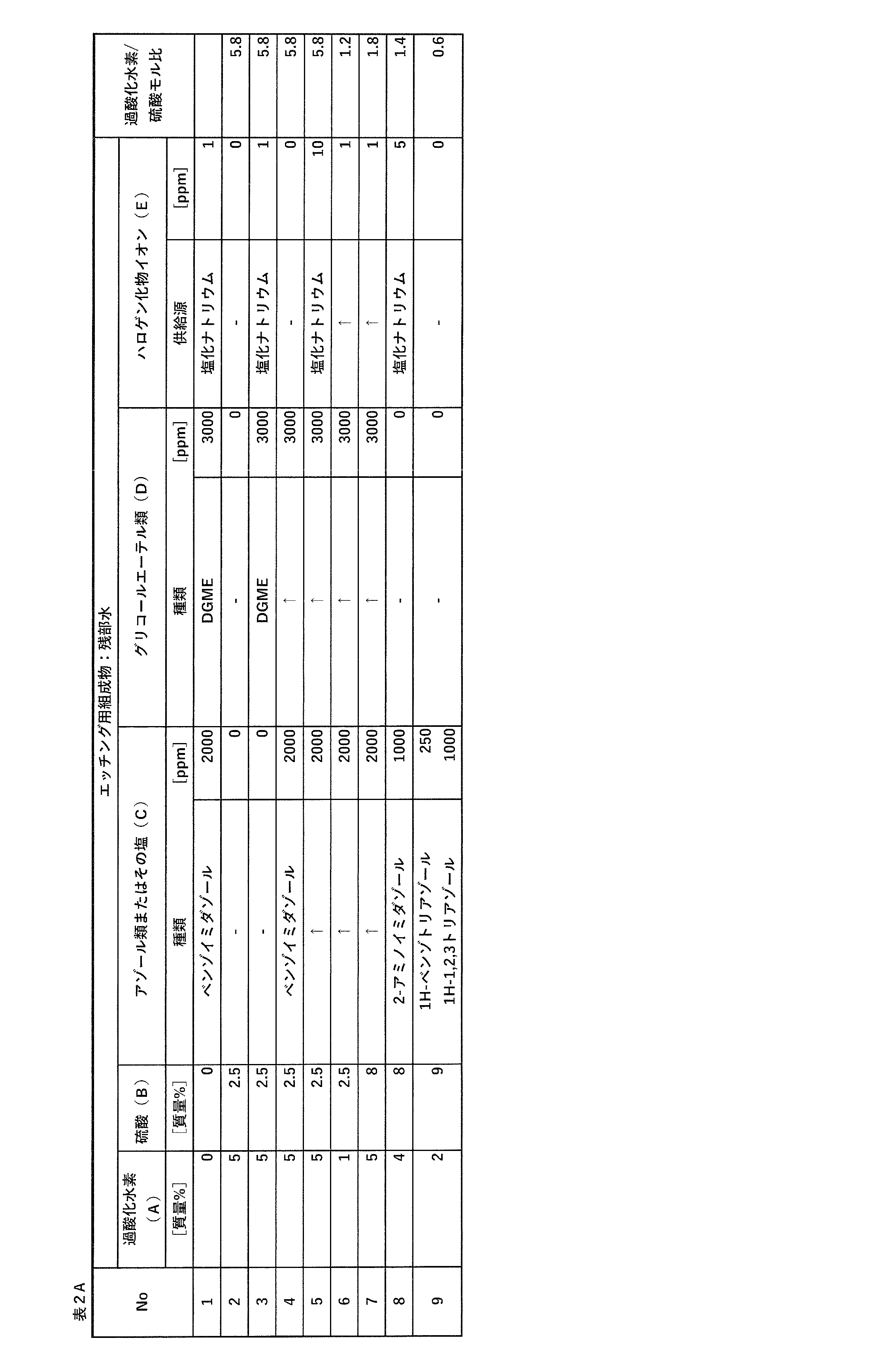
- Comparative Examples 1-9 An etching composition was prepared in the same manner as in Example except that the composition ratio shown in Table 2A was used, and an evaluation sample was used for etching. thickness and squareness), etch rate, and etch rate ratio were evaluated.
- the etching composition of the present invention it is possible to selectively remove the copper seed layer while suppressing thinning of the copper wiring and maintaining the rectangularity of the cross section of the wiring. Yes (Examples 1 to 24).
- the etching does not progress (Comparative Example 1), and when only the components (A) and (B) are included, or when the component (C) is not included. , the wiring height was greatly reduced, and the copper seed layer could not be selectively etched (Comparative Examples 2 and 3).
Landscapes
- Engineering & Computer Science (AREA)
- Chemical & Material Sciences (AREA)
- Manufacturing & Machinery (AREA)
- Microelectronics & Electronic Packaging (AREA)
- Materials Engineering (AREA)
- Organic Chemistry (AREA)
- Inorganic Chemistry (AREA)
- Chemical Kinetics & Catalysis (AREA)
- General Chemical & Material Sciences (AREA)
- Mechanical Engineering (AREA)
- Metallurgy (AREA)
- ing And Chemical Polishing (AREA)
- Weting (AREA)
- Manufacturing Of Printed Circuit Boards (AREA)
Abstract
Description
金属配線の微細化に対応可能な加工方法として、必要な箇所にのみ電解銅めっきにて銅配線パターンを形成するセミアディティブ工法(SAP: Semi Additive Process、以下「SAP」という)が知られている。中でも、近年では、ファインピッチ化にも対応可能なモディファイド-セミアディティブ工法(M-SAP: Modified-Semi Additive Process、以下「M-SAP」という)が注目されている。
SAPでは、まず、絶縁層上に、無電解銅めっき膜、場合によってはさらに極薄の電解銅めっき膜を形成して銅シード層を形成する。次に、銅シード層の上にフォトレジストを用いて銅配線を形成するためのレジストパターンを形成し、レジストパターン間に電解銅めっきにより銅配線パターンを形成する。その後、レジストパターンを除去し、露出した銅シード層を化学エッチングにより除去して、絶縁層上に微細な銅配線パターンを形成することができる。
M-SAPでは、まず、キャリア箔付きの電解銅箔を用いて、絶縁層上に電解銅箔を積層し、次いでこの電解銅箔を必要に応じてハーフエッチングにより極薄の銅薄層とし、その上に無電解銅めっき膜を形成して銅シード層を形成する。次に、銅シード層の上に銅配線を形成するためのレジストパターンを形成し、レジストパターン間に電解銅めっきにより銅配線パターンを形成する。その後、レジストパターンを除去し、露出した銅シード層を化学エッチングにより除去することにより、絶縁層上に微細な銅配線パターンを形成することができる。
このように、SAPまたはM-SAPでは、銅配線パターンを形成した後、銅シード層を除去する必要があるが、銅シード層を除去する際に、銅配線の高さや幅が減少し易く、配線断面の形状が矩形性を保持できない場合があった。
特許文献1では、過酸化水素および硫酸を主成分とし、添加剤としてアゾール類を含むエッチング液が、SAPにおける銅シード層の除去にあたって回路部分のやせ細りや裾引き形状を抑制できることが記載されている。しかし、加工精度をより高めるためには、銅シード層をより選択的にエッチングすることが求められている。
銅配線の微細化に対応可能な加工方法としてエンベデッドトレースサブストレート(ETS: Embedded Trace Substrate)工法(以下「ETS工法」という。)も知られている(特許文献2)。しかし、ETS工法の場合も、銅シード層としての電解銅箔上に形成した銅配線パターンを樹脂に埋め込んだ後、銅シード層としての電解銅箔をエッチングにより除去する必要があり、エッチングの際の、層間絶縁樹脂の側壁に沿った銅配線のエッチング(サイドエッチング)および銅配線上面のエッチングの程度によっては、配線断面の形状が矩形性を保持できない場合がある。このため、ETS工法においても、銅シード層としての電解銅箔を選択的にエッチングすることが求められている。
なお、本明細書において、「銅シード層」は、絶縁層上にめっき技術を用いて銅配線を形成する際に下地層として形成される銅の薄膜をいい、その形成方法については特に限定されない。この銅薄膜としては、例えば、電解銅箔、電解銅めっき膜、または無電解銅めっき膜のいずれでもよく、これらの組み合わせであってもよい。
[1]銅配線パターンと銅シード層とを有する基板から、銅シード層を選択的にエッチングするためのエッチング用組成物であって、
過酸化水素(A)、硫酸(B)、アゾール類またはその塩(C)、グリコールエーテル類(D)、ハロゲン化物イオン(E)、および水(F)を含み、
過酸化水素(A)の含有量が、エッチング用組成物の全量基準で0.1~10質量%であり、
硫酸(B)の含有量が、エッチング用組成物の全量基準で0.5~5質量%であり、
硫酸(B)に対する過酸化水素(A)の比が、モル比で表して、2以上であり、
ハロゲン化物イオン(E)の含有量が、エッチング用組成物の全量基準で0.01~3ppmである、
エッチング用組成物。
[2]アゾール類が、窒素原子を2個有する五員複素環またはその縮合複素環を有する複素環式化合物である、前記[1]に記載のエッチング用組成物。
[3]アゾール類が、ピラゾール類、イミダゾール類、およびベンゾイミダゾール類からなる群より選択される少なくとも1種である、前記[2]に記載のエッチング用組成物。
[4]アゾール類が、次式:
[式中、R1、R2、R3、R4、R5およびR6は、それぞれ互いに独立して、水素原子、C1~C6アルキル基、C6~C10アリール基、カルボキシル基、カルボキシC1~C6アルキル基、ニトロ基、ヒドロキシル基、C2~C7カルボン酸エステル、またはハロゲン原子である。]
で示される化合物からなる群より選ばれる1種以上である、前記[3]に記載のエッチング用組成物。
[5]アゾール類が、イミダゾール、1,2,4,5-テトラメチルイミダゾール、4-メチル-2-フェニルイミダゾール、ベンゾイミダゾール、1-メチルベンゾイミダゾール、2-メチルベンゾイミダゾール、5-メチルベンゾイミダゾール、2,5-ジメチルベンゾイミダゾール、5-ニトロベンゾイミダゾール、ピラゾール、および3,5-ジメチルピラゾールからなる群より選択される少なくとも1種である、前記[4]に記載のエッチング用組成物。
[6]アゾール類の含有量が、エッチング用組成物の全量基準で0.01~0.5質量%である、前記[1]から[5]のいずれか一項に記載のエッチング用組成物。
[7]グリコールエーテル類(D)が、エチレングリコールモノブチルエーテル、ジエチレングリコールモノメチルエーテル、ジエチレングリコールモノフェニルエーテル、およびジプロピレングリコールモノメチルエーテルからなる群より選択される少なくとも1種である、前記[1]から[6]のいずれか一項に記載のエッチング用組成物。
[8]グリコールエーテル類(D)の含有量が、エッチング用組成物の全量基準で0.01~1質量%である、前記[1]から[7]のいずれか一項に記載のエッチング用組成物。
[9]ハロゲン化物イオン(E)が、塩化物イオンである、前記[1]から[8]のいずれか一項に記載のエッチング用組成物。
[10]処理温度30℃における、式(1):
配線高さのエッチング速度比=Δ高さ/シード層厚み (1)
[式中、シード層厚みは、エッチングで除去される銅シード層の厚み(μm)を表し、Δ高さは、エッチングで銅シード層全てが丁度除去されるジャストエッチング時間において、エッチングで除去された銅配線の上面のエッチング厚み(μm)を表す。]
で定義される銅配線の配線高さのエッチング速度比が1.2以下である、前記[1]から[9]のいずれか一項に記載のエッチング用組成物。
[11]処理温度30℃における、式(2):
配線幅のエッチング速度比=Δ片幅/シード層厚み (2)
[式中、シード層厚みは、エッチングで除去される銅シード層の厚み(μm)を表し、Δ片幅は、エッチングで銅シード層全てが丁度除去されるジャストエッチング時間において、エッチングで除去された銅配線の横幅を片側分(1/2)に換算した値(μm)を表す。]
で定義される銅配線の配線幅のエッチング速度比が1.4以下である、前記[10]に記載のエッチング用組成物。
[12]銅シード層が、電解銅箔、電解銅めっき膜、および無電解銅めっき膜からなる群より選択される少なくとも1種である、前記[1]から[11]のいずれか一項に記載のエッチング用組成物。
[13]前記[1]から[12]のいずれか一項に記載のエッチング用組成物を用いて、銅配線パターンと銅シード層とを有する基板から、銅シード層を選択的にエッチングする工程を含む、配線基板の製造方法。
[14]銅シード層が、電解銅箔、電解銅めっき膜、および無電解銅めっき膜からなる群より選択される少なくとも1種である、前記[13]に記載の配線基板の製造方法。
[15]セミアディティブ工法(SAP)、モディファイド-セミアディティブ工法(M-SAP)、またはエンベデッドトレースサブストレート工法(ETS工法)において、前記[1]から[12]のいずれか一項に記載のエッチング用組成物を用いて、銅配線パターンと銅シード層とを有する基板から、銅シード層を選択的にエッチングして、配線回路を形成する、配線基板の製造方法。
本発明にかかるエッチング用組成物は、銅配線パターンと銅シード層とを有する基板から、銅シード層を選択的にエッチングするためのエッチング用組成物であって、
過酸化水素(A)、硫酸(B)、アゾール類またはその塩(C)、グリコールエーテル類(D)、ハロゲン化物イオン(E)、および水(F)を含み、
過酸化水素(A)の含有量が、エッチング用組成物の全量基準で0.1~10質量%であり、
硫酸(B)の含有量が、エッチング用組成物の全量基準で0.5~5質量%であり、
硫酸(B)に対する過酸化水素(A)の比が、モル比で表して、2以上であり、
ハロゲン化物イオン(E)の含有量が、エッチング用組成物の全量基準で0.01~3ppmであることを特徴とする。
本発明において、過酸化水素(A)(以下、単に(A)成分ということがある。)は、銅の酸化剤として機能する成分である。
(A)成分に特に制限はなく、工業用および電子工業用など、様々なグレードのものを使用することができる。一般的には過酸化水素水溶液として用いることが入手性および操作性の点で好ましい。
なお、本明細書において数値範囲を示したときは、上限値および下限値を適宜組み合わせることができ、それによって得られる数値範囲も開示されているものとする。
本発明において、硫酸(B)(以下、単に(B)成分ということがある。)は、過酸化水素(A)によって酸化された銅のエッチング剤として作用する成分である。
本発明において、アゾール類またはその塩(C)(以下、単に(C)成分ということがある。)は、銅配線の表面に吸着することにより、銅シード層を選択的に除去する機能を有することができる。
本発明において、アゾール類は、窒素を1個以上有する五員複素環またはその縮合複素環を有する複素環式化合物であり、前記五員複素環または縮合複素環を構成する原子が、アルキル基、カルボキシル基、カルボキシアルキル基、ニトロ基、ヒドロキシル基、カルボン酸エステル、ハロゲン原子などから選択される1種または2種以上の置換基を1個または2個以上有していてもよい。
アゾール類としては、例えば、ピラゾール類、イミダゾール類、ベンゾイミダゾール類、トリアゾール類、テトラゾール類などが挙げられる。これらの中でも、銅配線に対して銅シード層を選択的にエッチングできる点で、アゾール類は、窒素原子を2個有する五員複素環またはその縮合複素環を有する複素環式化合物であることが好ましく、特に、ピラゾール類、イミダゾール類、およびベンゾイミダゾール類からなる群より選択される少なくとも1種であることがより好ましい。
なお、(C)成分は、アゾール類の塩であってもよい。アゾール類の塩は、特に限定されないが、経済性の点から無機酸塩であることが好ましく、例えば、硝酸塩、硫酸塩、塩酸塩などが挙げられる。なお、アゾール類の塩が塩酸塩である場合、塩酸塩が有する塩化物イオンはハロゲン化物イオン(E)として機能することができる。
ピラゾール類としては、ピラゾール骨格を有しているものであればよく、特に限定されないが、例えば、次式:
[式中、R1、R2、R3およびR4は、それぞれ互いに独立して、水素原子、C1~C6アルキル基、C6~C10アリール基、カルボキシル基、カルボキシC1~C6アルキル基、ニトロ基、ヒドロキシル基、C2~C7カルボン酸エステル、またはハロゲン原子である。]
で示される化合物からなる群より選ばれる1種以上であることが好ましい。
「C6~C10アリール基」は、炭素数6~10のアリール基を意味する。C6~C10アリール基としては、フェニル基、1-ナフチル基、2-ナフチル基、インデニル基、ビフェニル基、アントリル基、フェナントリル基などが挙げられる。これらの中でも、フェニル基が好ましい。
「カルボキシC1~C6アルキル基」は、カルボキシル基を有する炭素数1~6のアルキル基を意味する。C1~C6アルキル基としては、前述したものと同じものが挙げられる。カルボキシC1~C6アルキル基の具体例としては、カルボキシメチル基(-CH2-COOH)、カルボキシエチル基(-CH2CH2-COOH)が好ましい。
「C2~C7カルボン酸エステル」は、-COOR(Rは、C1~C6アルキル基である)で表される基を意味する。C1~C6アルキル基としては、前述したものと同じものが挙げられる。C2~C7カルボン酸エステルの具体例としては、カルボン酸メチル、カルボン酸エチルが好ましい。
「ハロゲン原子」は、フッ素原子、塩素原子、臭素原子、ヨウ素原子のいずれでもよく、特に塩素原子、臭素原子が好ましい。
ピラゾール類の例としては、ピラゾール、3,5-ジメチルピラゾールなどが挙げられる。
イミダゾール類としては、イミダゾール骨格を有しているものであればよく、特に限定されないが、例えば、次式:
[式中、R1、R2、R3およびR4は、それぞれ互いに独立して、水素原子、C1~C6アルキル基、C6~C10アリール基、カルボキシル基、カルボキシC1~C6アルキル基、ニトロ基、ヒドロキシル基、C2~C7カルボン酸エステル、またはハロゲン原子である。]
で示される化合物からなる群より選ばれる1種以上であることが好ましい。
イミダゾール類の例としては、イミダゾール、1,2,4,5-テトラメチルイミダゾール、4-メチル-2-フェニルイミダゾールなどが挙げられる。
ベンゾイミダゾール類としては、ベンゾイミダゾール骨格を有しているものであればよく、特に限定されないが、例えば、次式:

[式中、R1、R2、R3、R4、R5およびR6は、それぞれ互いに独立して、水素原子、C1~C6アルキル基、C6~C10アリール基、カルボキシル基、カルボキシC1~C6アルキル基、ニトロ基、ヒドロキシル基、C2~C7カルボン酸エステル、またはハロゲン原子である。]
で示される化合物からなる群より選ばれる1種以上であることが好ましい。
ベンゾイミダゾール類の例としては、ベンゾイミダゾール、1-メチルベンゾイミダゾール、2-メチルベンゾイミダゾール、5-メチルベンゾイミダゾール、2,5-ジメチルベンゾイミダゾール、5-ニトロベンゾイミダゾール硝酸塩などが挙げられる。
トリアゾール類としては、トリアゾール骨格を有しているものであればよく、特に限定されない。例えば、1,2,4-トリアゾールなどが挙げられる。
ベンゾトリアゾール類としては、ベンゾトリアゾール骨格を有しているものであればよく、特に限定されない。例えば、1H-ベンゾトリアゾール、5-メチル-1H-ベンゾトリアゾールなどが挙げられる。
テトラゾール類としては、テトラゾール骨格を有しているものであればよく、特に限定されない。例えば、1H-テトラゾール、5-メチル-1H-テトラゾール、5-フェニル-1H-テトラゾール、1,5-ペンタメチレンテトラゾールなどが挙げられる。
前述したとおり、(C)成分としては、アゾール類の塩であってもよい。(C)成分としては、4-メチル-2-フェニルイミダゾール、ベンゾイミダゾール、1-メチルベンゾイミダゾール、2-メチルベンゾイミダゾール、5-メチルベンゾイミダゾール、2,5-ジメチルベンゾイミダゾール、5-ニトロベンゾイミダゾール硝酸塩、およびピラゾールからなる群より選択される少なくとも1種であることが特に好ましい。
本発明において、グリコールエーテル類(D)(以下、単に(D)成分ということがある。)は、エッチング処理における基板の面内および/または表裏の銅の溶解量を均一にする効果を奏しうる。具体的には、エッチング処理における基板の面内および/または表裏の銅配線のエッチング速度、エッチング量を均一にできる効果を奏しうる。このため、基板の面内および/または表裏の銅配線の細りの程度、配線断面の矩形性を、均一にできる効果を奏しうる。
(D)成分としては、特に限定されないが、エチレングリコールモノブチルエーテル、ジエチレングリコールモノメチルエーテル、ジエチレングリコールモノフェニルエーテル、およびジプロピレングリコールモノメチルエーテルからなる群より選択される少なくとも1種であることが好ましい。
(D)成分の含有量は、エッチング用組成物の全量基準(質量基準)で0.01~1質量%(100~10000ppm)の範囲であることが好ましく、より好ましくは0.05~0.75質量%(500~7500ppm)、さらに好ましくは0.1~0.5質量%(1000~5000ppm)の範囲である。(D)成分の含有量が上記範囲内にあることで、銅配線の細りを抑制しつつ、配線断面の矩形性を保持しながら、銅シード層を選択的に除去することができる。また、本発明の好ましい態様によれば、(D)成分の含有量が上記範囲内にあることで、エッチング処理時のスプレー圧などの物理的条件による影響を受けにくい。(D)成分を2種以上用いる場合は、それらの合計量が上記範囲内であればよい。
本発明において、ハロゲン化物イオン(E)(以下、単に(E)成分ということがある。)は、エッチング速度を安定化させる作用を有する。
(E)成分としては、フッ化物イオン、塩化物イオン、臭化物イオン、ヨウ化物イオンが好ましく、塩化物イオン、臭化物イオンがより好ましく、塩化物イオンが特に好ましい。
(E)成分の供給源(以下、ハロゲン化物イオン源ということがある)としては、塩酸、臭化水素酸等の酸;塩化ナトリウム、塩化アンモニウム、塩化カルシウム、塩化カリウム、臭化カリウム、フッ化ナトリウム、ヨウ化カリウム、塩化第二銅、臭化第二銅などの塩が挙げられる。これらの中でも、塩酸および塩化ナトリウムからなる群より選択される少なくとも1種であることが好ましい。
なお、例えば、アゾール類またはその塩(C)が、ハロゲン化物塩である場合、(C)成分から(E)成分が供給されてもよい。この場合、(C)成分は、ハロゲン化物イオン源としても使用することができる。
また、本発明においては、銅シード層をエッチングする際に銅が溶解するため、エッチング用組成物中の銅濃度の変動を抑える目的であらかじめ銅イオンを添加してもよく、塩化第二銅および臭化第二銅は、ハロゲン化物イオン源と銅イオン源の両方の作用を有するものとして使用することができる。
ハロゲン化物イオン(E)は、1種を単独で用いてもよく、2種以上を組み合わせて用いてもよい。
本発明に用いられる水(F)(以下、単に(F)成分ということがある。)としては、特に制限されないが、蒸留、イオン交換処理、フィルター処理、各種吸着処理などによって、金属イオンや有機不純物、パーティクル粒子などが除去された水が好ましく、特に純水、または超純水が好ましい。水の含有量は他の成分の残部であり特に限定されないが、エッチング用組成物の全量基準で85~99質量%の範囲であることが好ましい。
本発明のエッチング用組成物は、上記成分の他、必要に応じて、エッチング用組成物に通常用いられる各種添加剤の1種以上を、上記したエッチング用組成物の効果を害しない範囲で含むことができる。
また、大きくpHが変わらない範囲であれば、微量のアルカリを加えてもよい。
さらに、本発明のエッチング用組成物には、アルコール類、フェニル尿素、有機カルボン酸類、有機アミン化合物類等の公知の過酸化水素安定剤、およびエッチング速度調整剤等を必要に応じて添加してもよい。
なお、本発明のエッチング液は溶解液であることが好ましく、研磨粒子等の固形粒子は含有しない。
本発明のエッチング用組成物は、(A)成分、(B)成分、(C)成分、(D)成分、(E)成分、(F)成分、および必要に応じて添加されるその他の成分を、均一に攪拌、混合することで調製できる。これらの成分の混合における攪拌方法は特に制限されず、エッチング用組成物の調製において通常用いられる攪拌方法を採用することができる。
本発明のエッチング用組成物は、銅配線パターンと銅シード層とを有する基板から、銅シード層を選択的にエッチングするためのエッチング用組成物として用いることができる。
本発明のエッチング用組成物により選択的にエッチングされる銅シード層としては、電解銅箔、電解銅めっき膜、無電解銅めっき膜またはこれらの2種以上の組み合わせが好ましい。
なお、本明細書において「選択的に」とは、銅シード層のエッチング速度が、銅配線のエッチング速度よりも大きいことをいう。
例えば、本発明において、銅シード層のエッチング速度に対する銅配線のエッチング速度の比は、処理温度30℃における、銅シード層のエッチング速度を基準とした、銅配線の配線高さのエッチング速度比および配線幅のエッチング速度比で評価することができる。配線高さのエッチング速度比および配線幅のエッチング速度比は、下記の式(1)および式(2)で定義される。
配線高さのエッチング速度比=Δ高さ/シード層厚み (1)
配線幅のエッチング速度比=Δ片幅/シード層厚み (2)
[式中、シード層厚みは、エッチングで除去される銅シード層の厚み(μm)を表し、Δ高さは、エッチングで銅シード層全てが丁度除去されるジャストエッチング時間において、エッチングで除去された銅配線の上面のエッチング厚み(μm)を表し、Δ片幅は、エッチングで銅シード層全てが丁度除去されるジャストエッチング時間において、エッチングで除去された銅配線の横幅を片側分(1/2)に換算した値(μm)を表す。]
本発明において、配線高さのエッチング速度比は、1.2以下であることが好ましい。さらに、配線幅のエッチング速度比は、1.4以下であることが好ましく、より好ましくは1.0以下である。本発明においては、配線高さのエッチング速度比が上記範囲を満たしていることが好ましく、配線高さのエッチング速度比および配線幅のエッチング速度比の両方が上記範囲を満たしていることがより好ましい。
本発明の好ましい態様によれば、本発明のエッチング用組成物を用いて銅シード層をエッチングすることで、銅配線の細りを抑制しつつ、配線断面の矩形性を保持しながら、銅シード層を選択的に除去することができる。
本発明のエッチング用組成物によって除去するのに適した銅シード層の厚みは特に制限されないが、通常1.5~15μmであり、好ましくは1.5~10μm、より好ましくは1.5~5μmである。
本発明にかかる配線基板の製造方法は、前記エッチング用組成物を用いて、銅配線パターンと銅シード層とを有する基板から、銅シード層を選択的にエッチングする工程を含むことを特徴とする。
エッチング用組成物およびエッチング対象である銅シード層については、前記「1.エッチング用組成物」で述べたとおりである。
図1は、SAPにおいて、銅配線パターンと銅シード層とを有する基板から、銅シード層を選択的にエッチングして配線回路を形成する、配線基板の製造方法を説明するための図である。図1では、説明のために必要な構造のみを模式的に表している。
次に、無電解銅めっき膜(2)、または電解銅めっき膜を形成する場合は電解銅めっき膜の表面にドライフィルムレジスト(3)を形成し(図1(d))、これを露光および現像して、レジストパターン(3a)を形成する(図1(e))。
続いて、レジストパターン(3a)間の銅シード層上に電解銅めっきを施し、電解銅めっき膜(4)を形成する(図1(f))。
次いで、レジストパターン(3a)を剥離液により剥離して、銅配線パターン(4a)を形成する(図1(g))。
最後に、本発明のエッチング用組成物を、銅シード層の表面に適用して、銅シード層の露出部分を除去することで銅配線パターン(4a)が形成された配線基板(10)を製造することができる(図1(h))。
図2は、M-SAPにおいて、銅配線パターンと銅シード層とを有する基板から、銅シード層を選択的にエッチングして配線回路を形成する、配線基板の製造方法を説明するための図である。図2においても、説明のために必要な構造のみを模式的に表している。
次に、ビアまたはトレンチ(1a)の内壁を含む銅薄層(6)上に、無電解銅めっきを施し、無電解銅めっき膜(2)を形成する(図2(d))。また、図示しないが、無電解銅めっき膜(2)の上にさらに電解銅めっき膜(図示しない)を形成してもよい。電解銅めっき膜を形成しない場合は、銅薄層(6)および無電解銅めっき膜(2)を「銅シード層」とする。電解銅めっき膜を形成する場合は、銅薄層(6)、無電解銅めっき膜(2)および電解銅めっき膜を「銅シード層」とする。
次に、無電解銅めっき膜(2)、または電解銅めっき膜を形成する場合は電解銅めっき膜(図示しない)の表面にドライフィルムレジスト(3)を形成し(図2(e))、これを露光および現像して、レジストパターン(3a)を形成する(図2(f))。
続いて、レジストパターン(3a)間の銅シード層上に電解銅めっきを施し、電解銅めっき膜(4)を形成する(図2(g))。
次いで、レジストパターン(3a)を剥離液により剥離して、銅配線パターン(4a)を形成する(図2(h))。
最後に、本発明のエッチング用組成物を、銅シード層の表面に適用して、銅シード層の露出部分を除去することで銅配線パターン(4a)が形成された配線基板(10)を製造することができる(図2(i))。
図3は、ETS工法において銅配線パターンと銅シード層とを有する基板から、銅シード層を選択的にエッチングして配線回路を形成する、配線基板の製造方法を説明するための図である。図3においても、説明のために必要な構造のみを模式的に表している。
その後、レジストパターン(3a)が形成されていない電解銅箔(5)の露出部分に電解銅めっきを施し、電解銅めっき膜(4)を形成する(図3(c))。
次いで、レジストパターン(3a)を剥離液により剥離して、銅配線から構成される銅配線パターン(4a)を形成する(図3(d))。
その後、絶縁樹脂基板(1)とキャリア箔(5a)を剥がし(図3(f))、最後に、電解銅箔(5)を、本発明のエッチング用組成物を用いてエッチバックして、銅配線パターン(4a)が埋め込まれたプリント配線板(10)を得ることができる(図3(g))。
(1)エッチング用組成物の調製
表1Aに記載の組成比で各成分を混合し、撹拌して均一な状態として、エッチング用組成物を調製した。

<M-SAPにおける評価用サンプル(実施例1~13、実施例15~24、比較例1~9)>
以下のようにして、実施例1~13、実施例15~24および比較例1~9のエッチング用組成物の評価用サンプルを準備した。
まず、厚さ3μmの電解銅箔を有するキャリア箔付き極薄銅箔「Micro Thin 18EX」(三井金属鉱業株式会社製)を、絶縁樹脂基板(デタッチコア)に対し、電解銅箔側が接するようにラミネートした。
次いで、キャリア箔を剥離し、露出した電解銅箔上に、無電解銅めっき(0.6μm)および電解銅めっき(3.4μm)を、合計で厚さ4μmとなるように施して、厚さ7μmの銅シード層を形成した。
その後、銅シード層上にドライフィルムレジストをラミネートし、ライン/スペース(L/S)=45/15μmの配線デザインでドライフィルムレジストを露光した。炭酸ナトリウム水溶液を用いて露光後のドライフィルムレジストを現像し、レジストパターンを形成した。
次いで、レジストで被覆されていない銅シード層の露出部分に、電解銅めっきを施し、配線高さが20μmとなるように電解銅めっき膜を形成した。
その後、ドライフィルム剥離液「R-100S」(三菱瓦斯化学株式会社製)を用いてレジストパターンを剥離し、銅シード層上に銅配線が形成された基板(評価用サンプル)を得た。
評価用サンプルにおける銅配線幅は43.8μmであり、銅シード層上面からの銅配線高さは21.3μmであった。
<ETS工法における評価用サンプル(実施例14)>
以下のようにして、実施例14のエッチング用組成物の評価用サンプルを準備した。
まず、厚さ5μmの電解銅箔を有するキャリア箔付き極薄銅箔「MT18SD-H-T5」(三井金属鉱業株式会社製)を、厚さ100μmのデタッチコア(基材:「HL-832NSF」)(三菱瓦斯化学株式会社製)に対しキャリア箔側が接するようにラミネートした。
次いで、電解銅箔の表面にドライフィルムレジストをラミネートし、ライン/スペース(L/S)=10/10μmの配線デザインでドライフィルムレジストを露光した。炭酸ナトリウム水溶液を用いて露光後のドライフィルムレジストを現像し、レジストパターンを形成した。
次いで、レジストで被覆されていない電解銅箔(銅シード層)の露出部分に、電解銅めっきを施し、配線高さが10μmとなるように電解銅めっき膜を形成した。
その後、ドライフィルム剥離液「R-100S」(三菱瓦斯化学株式会社製)を用いてレジストパターンを剥離し、電解銅箔上に銅配線を形成した。
次いで、得られた構造体を反転させ、銅配線がプリプレグ「GHPL-830NS SH65」(三菱瓦斯化学株式会社製)に埋め込まれるように積層した。なお、銅配線をプリプレグに積層する際に用いた、銅配線とは反対側にプリプレグに積層されている外層銅箔としては、厚さ5μmの電解銅箔を有するキャリア箔付き極薄銅箔「MT18Ex」(三井金属鉱業株式会社製)を、電解銅箔がプリプレグ側となるようにして使用した。
その後、デタッチコアとキャリア箔を剥がし、電解銅箔を表面に有し、銅配線が埋め込まれた基板を作製した。
得られた基板は、20μmピッチで10~10.5μmの配線幅で銅配線が形成されていた。
評価用サンプルを、前記(1)で調製したエッチング用組成物を用いて、処理温度30℃で、スプレーエッチングマシンにより、エッチング処理を施した。スプレー圧は実施例4では0.05MPaとし、その他の実施例および比較例では0.15MPaとした。エッチングの終点は、光学顕微鏡(オリンパス株式会社製「MX-63L」)を用いて観察し、銅配線間の銅シード層の残銅がなくなった時点とした(ジャストエッチング時間)。
エッチング用組成物から評価用サンプルを取り出し、超純水に10秒間、5質量%の硫酸に10秒間、超純水に10秒間浸漬して、洗浄した。超純水から評価用サンプルを取り出し、窒素ブローで評価用サンプルを乾燥させた。
実施例および比較例の各評価用サンプルにおけるエッチング処理後の銅配線の配線幅および高さを、配線断面方向から、SEM(株式会社日立ハイテク製「S-3700」)を用いて測定し、以下の基準で評価した。
<幅>
◎:30μm以上
〇:25μm以上30μm未満
×:25μm未満
<高さ>
◎:20μm以上
×:20μm未満
エッチング処理後の銅配線の配線断面をSEM(株式会社日立ハイテク製「S-3700」)で観察し、配線断面形状の矩形性を目視で評価した。矩形性は以下の基準で評価した。
<矩形性>
◎:矩形性を保持していた
〇:やや台形状になったが、矩形性を保持していた
×:台形状になり、矩形性を保持できなかった、もしくはアンダーカットまたはサイドエッチングが発生した
なお、評価基準の具体例を、SAP、M-SAPの場合と、ETS工法の場合について、図4にそれぞれ示す。
銅シード層の厚み(μm)を、ジャストエッチング時間(min)で除することにより、銅シード層のエッチング速度(ER、μm/min)を求めた。
次式に従い、配線幅のエッチング速度比および配線高さのエッチング速度比を求め、以下の基準で評価した。
配線高さのエッチング速度比=Δ高さ/シード層厚み (1)
配線幅のエッチング速度比=Δ片幅/シード層厚み (2)
<配線高さのエッチング速度比>
◎:1.2以下
×:1.2超
<配線幅のエッチング速度比>
◎:1.0以下
〇:1.0超1.4以下
×:1.4超
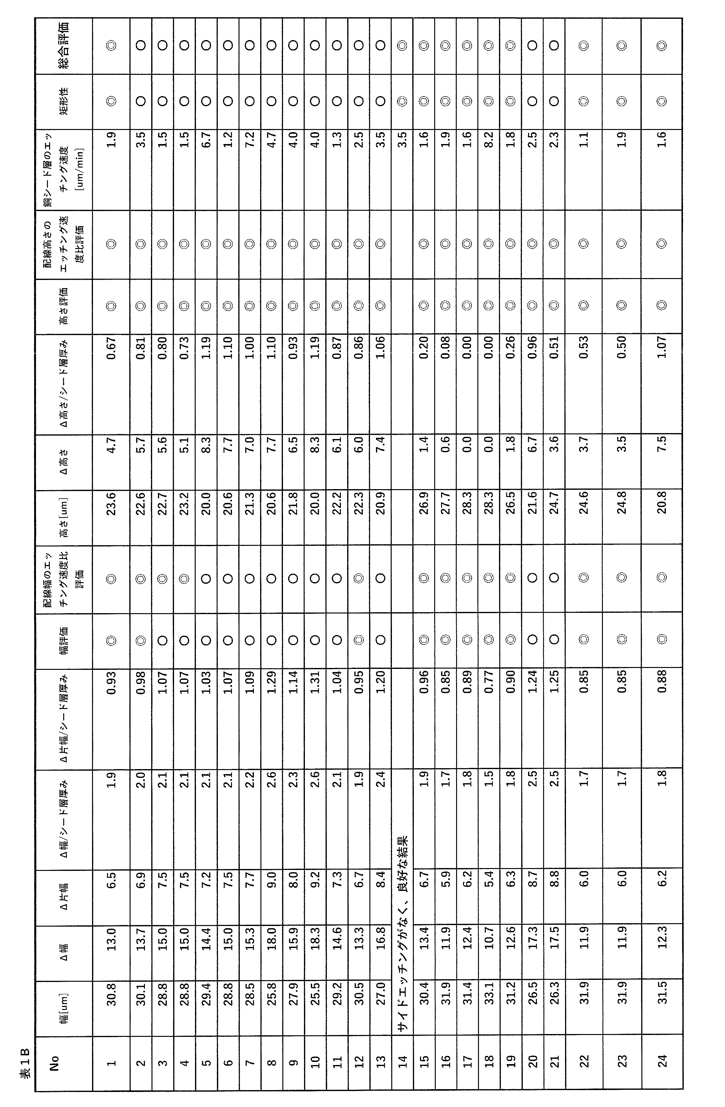
表2Aに記載の組成比としたこと以外は、実施例と同様にしてエッチング用組成物を調製し、評価用サンプルを用いてエッチング処理を行ない、エッチング処理後の銅配線の形状(幅、高さおよび矩形性)、エッチング速度、およびエッチング速度比を評価した。
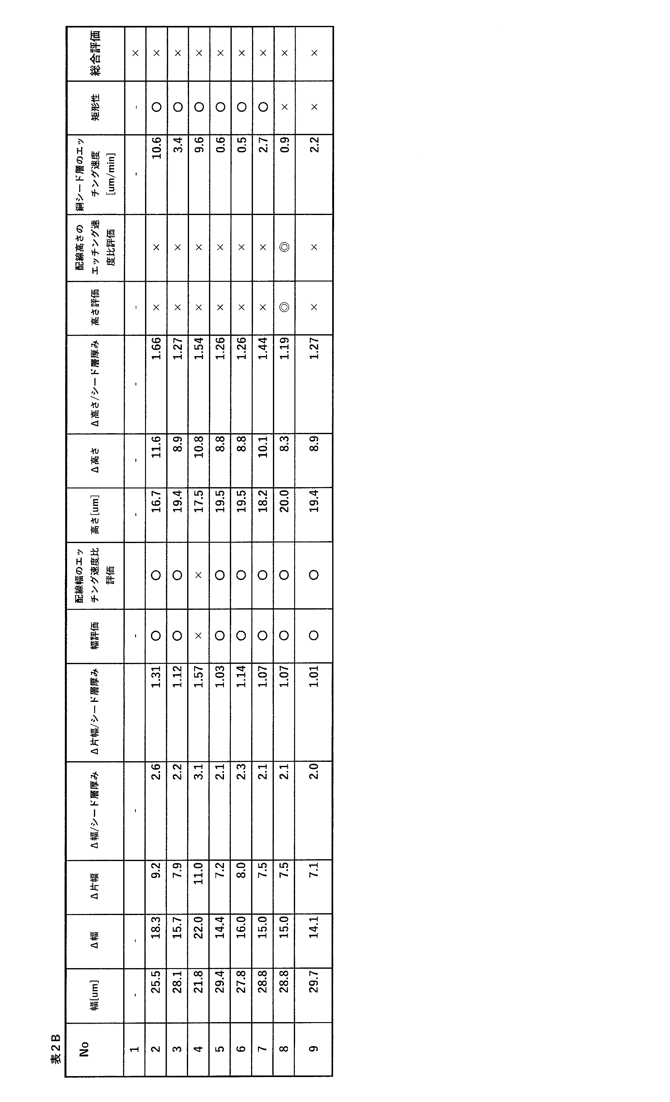
一方、(A)成分および(B)成分を含まない場合はエッチングが進行せず(比較例1)、(A)成分および(B)成分のみである場合、あるいは(C)成分を含まない場合、配線高さが大きく減少してしまい、銅シード層を選択的にエッチングすることができなかった(比較例2、3)。
(E)成分を含まない場合は、配線幅および配線高さ共に大きく減少し、銅シード層を選択的にエッチングすることができなかった(比較例4)。また、(E)成分の含有量が所定の範囲を超えた場合、配線高さが大きく減少してしまい、銅シード層を選択的にエッチングすることができなかった(比較例5)。
(A)成分/(B)成分が所定の範囲より小さい場合も、銅シード層を選択的にエッチングすることができなかった(比較例6、7)。
(D)成分を含まず、(A)成分/(B)成分が所定の範囲より小さい場合は、矩形性を保持することができなかった(比較例8)。
また、(D)成分および(E)成分を含まず、(A)成分/(B)成分が所定の範囲より小さい場合は、配線高さが大きく減少してしまい、矩形性も保持することができなかった(比較例9)。
1a ビアまたはトレンチ
2 無電解銅めっき膜
3 ドライフィルムレジスト
3a レジストパターン
4 電解銅めっき膜
4a 銅配線パターン
5 電解銅箔
5a キャリア箔
6 銅薄層
7 層間絶縁樹脂
10 配線基板またはプリント配線板
Claims (15)
- 銅配線パターンと銅シード層とを有する基板から、銅シード層を選択的にエッチングするためのエッチング用組成物であって、
過酸化水素(A)、硫酸(B)、アゾール類またはその塩(C)、グリコールエーテル類(D)、ハロゲン化物イオン(E)、および水(F)を含み、
過酸化水素(A)の含有量が、エッチング用組成物の全量基準で0.1~10質量%であり、
硫酸(B)の含有量が、エッチング用組成物の全量基準で0.5~5質量%であり、
硫酸(B)に対する過酸化水素(A)の比が、モル比で表して、2以上であり、
ハロゲン化物イオン(E)の含有量が、エッチング用組成物の全量基準で0.01~3ppmである、
エッチング用組成物。 - アゾール類が、窒素原子を2個有する五員複素環またはその縮合複素環を有する複素環式化合物である、請求項1に記載のエッチング用組成物。
- アゾール類が、ピラゾール類、イミダゾール類、およびベンゾイミダゾール類からなる群より選択される少なくとも1種である、請求項2に記載のエッチング用組成物。
- アゾール類が、次式:

[式中、R1、R2、R3、R4、R5およびR6は、それぞれ互いに独立して、水素原子、C1~C6アルキル基、C6~C10アリール基、カルボキシル基、カルボキシC1~C6アルキル基、ニトロ基、ヒドロキシル基、C2~C7カルボン酸エステル、またはハロゲン原子である。]
で示される化合物からなる群より選ばれる1種以上である、請求項3に記載のエッチング用組成物。 - アゾール類が、イミダゾール、1,2,4,5-テトラメチルイミダゾール、4-メチル-2-フェニルイミダゾール、ベンゾイミダゾール、1-メチルベンゾイミダゾール、2-メチルベンゾイミダゾール、5-メチルベンゾイミダゾール、2,5-ジメチルベンゾイミダゾール、5-ニトロベンゾイミダゾール、ピラゾール、および3,5-ジメチルピラゾールからなる群より選択される少なくとも1種である、請求項4に記載のエッチング用組成物。
- アゾール類の含有量が、エッチング用組成物の全量基準で0.01~0.5質量%である、請求項1から5のいずれか一項に記載のエッチング用組成物。
- グリコールエーテル類(D)が、エチレングリコールモノブチルエーテル、ジエチレングリコールモノメチルエーテル、ジエチレングリコールモノフェニルエーテル、およびジプロピレングリコールモノメチルエーテルからなる群より選択される少なくとも1種である、請求項1から6のいずれか一項に記載のエッチング用組成物。
- グリコールエーテル類(D)の含有量が、エッチング用組成物の全量基準で0.01~1質量%である、請求項1から7のいずれか一項に記載のエッチング用組成物。
- ハロゲン化物イオン(E)が、塩化物イオンである、請求項1から8のいずれか一項に記載のエッチング用組成物。
- 処理温度30℃における、式(1):
配線高さのエッチング速度比=Δ高さ/シード層厚み (1)
[式中、シード層厚みは、エッチングで除去される銅シード層の厚み(μm)を表し、Δ高さは、エッチングで銅シード層全てが丁度除去されるジャストエッチング時間において、エッチングで除去された銅配線の上面のエッチング厚み(μm)を表す。]
で定義される銅配線の配線高さのエッチング速度比が1.2以下である、請求項1から9のいずれか一項に記載のエッチング用組成物。 - 処理温度30℃における、式(2):
配線幅のエッチング速度比=Δ片幅/シード層厚み (2)
[式中、シード層厚みは、エッチングで除去される銅シード層の厚み(μm)を表し、Δ片幅は、エッチングで銅シード層全てが丁度除去されるジャストエッチング時間において、エッチングで除去された銅配線の横幅を片側分(1/2)に換算した値(μm)を表す。]
で定義される銅配線の配線幅のエッチング速度比が1.4以下である、請求項10に記載のエッチング用組成物。 - 銅シード層が、電解銅箔、電解銅めっき膜、および無電解銅めっき膜からなる群より選択される少なくとも1種である、請求項1から11のいずれか一項に記載のエッチング用組成物。
- 請求項1から12のいずれか一項に記載のエッチング用組成物を用いて、銅配線パターンと銅シード層とを有する基板から、銅シード層を選択的にエッチングする工程を含む、配線基板の製造方法。
- 銅シード層が、電解銅箔、電解銅めっき膜、および無電解銅めっき膜からなる群より選択される少なくとも1種である、請求項13に記載の配線基板の製造方法。
- セミアディティブ工法(SAP)、モディファイド-セミアディティブ工法(M-SAP)、またはエンベデッドトレースサブストレート工法(ETS工法)において、請求項1から12のいずれか一項に記載のエッチング用組成物を用いて、銅配線パターンと銅シード層とを有する基板から、銅シード層を選択的にエッチングして、配線回路を形成する、配線基板の製造方法。
Priority Applications (4)
| Application Number | Priority Date | Filing Date | Title |
|---|---|---|---|
| US18/840,565 US20250163322A1 (en) | 2022-02-25 | 2023-02-22 | Etching composition and method for producing wiring board using same |
| CN202380022864.0A CN118765338A (zh) | 2022-02-25 | 2023-02-22 | 蚀刻用组合物和使用其的布线基板的制造方法 |
| KR1020247024565A KR20240158224A (ko) | 2022-02-25 | 2023-02-22 | 에칭용 조성물 및 그것을 이용한 배선기판의 제조방법 |
| JP2024503185A JPWO2023163003A1 (ja) | 2022-02-25 | 2023-02-22 |
Applications Claiming Priority (2)
| Application Number | Priority Date | Filing Date | Title |
|---|---|---|---|
| JP2022-027613 | 2022-02-25 | ||
| JP2022027613 | 2022-02-25 |
Publications (1)
| Publication Number | Publication Date |
|---|---|
| WO2023163003A1 true WO2023163003A1 (ja) | 2023-08-31 |
Family
ID=87765975
Family Applications (1)
| Application Number | Title | Priority Date | Filing Date |
|---|---|---|---|
| PCT/JP2023/006336 Ceased WO2023163003A1 (ja) | 2022-02-25 | 2023-02-22 | エッチング用組成物およびそれを用いた配線基板の製造方法 |
Country Status (6)
| Country | Link |
|---|---|
| US (1) | US20250163322A1 (ja) |
| JP (1) | JPWO2023163003A1 (ja) |
| KR (1) | KR20240158224A (ja) |
| CN (1) | CN118765338A (ja) |
| TW (1) | TW202342701A (ja) |
| WO (1) | WO2023163003A1 (ja) |
Citations (4)
| Publication number | Priority date | Publication date | Assignee | Title |
|---|---|---|---|---|
| JPH01292890A (ja) * | 1988-05-20 | 1989-11-27 | Mitsubishi Gas Chem Co Inc | 薄銅張回路基板の製造法 |
| JP2005015860A (ja) * | 2003-06-26 | 2005-01-20 | Ebara Densan Ltd | 銅及び銅合金の鏡面仕上げエッチング液 |
| JP2012229460A (ja) * | 2011-04-25 | 2012-11-22 | Mitsubishi Gas Chemical Co Inc | 銅または銅合金表面用処理剤 |
| WO2019208461A1 (ja) * | 2018-04-24 | 2019-10-31 | 三菱瓦斯化学株式会社 | 銅箔用エッチング液およびそれを用いたプリント配線板の製造方法ならびに電解銅層用エッチング液およびそれを用いた銅ピラーの製造方法 |
Family Cites Families (1)
| Publication number | Priority date | Publication date | Assignee | Title |
|---|---|---|---|---|
| JP4430990B2 (ja) | 2004-06-29 | 2010-03-10 | 株式会社荏原電産 | セミアディティブ工法用回路形成エッチング液 |
-
2023
- 2023-02-22 JP JP2024503185A patent/JPWO2023163003A1/ja active Pending
- 2023-02-22 CN CN202380022864.0A patent/CN118765338A/zh active Pending
- 2023-02-22 TW TW112106380A patent/TW202342701A/zh unknown
- 2023-02-22 KR KR1020247024565A patent/KR20240158224A/ko active Pending
- 2023-02-22 WO PCT/JP2023/006336 patent/WO2023163003A1/ja not_active Ceased
- 2023-02-22 US US18/840,565 patent/US20250163322A1/en active Pending
Patent Citations (4)
| Publication number | Priority date | Publication date | Assignee | Title |
|---|---|---|---|---|
| JPH01292890A (ja) * | 1988-05-20 | 1989-11-27 | Mitsubishi Gas Chem Co Inc | 薄銅張回路基板の製造法 |
| JP2005015860A (ja) * | 2003-06-26 | 2005-01-20 | Ebara Densan Ltd | 銅及び銅合金の鏡面仕上げエッチング液 |
| JP2012229460A (ja) * | 2011-04-25 | 2012-11-22 | Mitsubishi Gas Chemical Co Inc | 銅または銅合金表面用処理剤 |
| WO2019208461A1 (ja) * | 2018-04-24 | 2019-10-31 | 三菱瓦斯化学株式会社 | 銅箔用エッチング液およびそれを用いたプリント配線板の製造方法ならびに電解銅層用エッチング液およびそれを用いた銅ピラーの製造方法 |
Also Published As
| Publication number | Publication date |
|---|---|
| US20250163322A1 (en) | 2025-05-22 |
| JPWO2023163003A1 (ja) | 2023-08-31 |
| KR20240158224A (ko) | 2024-11-04 |
| TW202342701A (zh) | 2023-11-01 |
| CN118765338A (zh) | 2024-10-11 |
Similar Documents
| Publication | Publication Date | Title |
|---|---|---|
| CN100459068C (zh) | 蚀刻剂、补充液以及用它们制造铜布线的方法 | |
| KR100868137B1 (ko) | 구리 및 구리 합금의 표면 처리제 | |
| JP5505847B2 (ja) | エッチング剤 | |
| US6902626B2 (en) | Method for roughening copper surface | |
| JP6424559B2 (ja) | エッチング用組成物及びそれを用いたプリント配線板の製造方法 | |
| JP2006009122A (ja) | セミアディティブ工法用回路形成エッチング液 | |
| JP4434632B2 (ja) | プリント配線板の製造方法 | |
| KR101162370B1 (ko) | 세미 어디티브법 프린트 배선 기판의 제조에서의 에칭 제거방법 및 에칭액 | |
| JP4431860B2 (ja) | 銅および銅合金の表面処理剤 | |
| JP2007180172A (ja) | 基板の製造方法 | |
| JP2011038124A (ja) | 金属表面処理剤 | |
| KR20240158224A (ko) | 에칭용 조성물 및 그것을 이용한 배선기판의 제조방법 | |
| JP7505836B1 (ja) | エッチング液、補給液及び銅配線の形成方法 | |
| JP2010196119A (ja) | 金属表面処理剤 | |
| WO2023090306A1 (ja) | 圧延銅箔の粗化液、粗化銅箔の製造方法 | |
| KR20230039882A (ko) | 구리 또는 구리 합금용 에칭액 | |
| JP2005029852A (ja) | 銅および銅合金のエッチング液 | |
| HK1074224B (en) | Etchant, replenishment solution and method for producing copper wiring using the same |
Legal Events
| Date | Code | Title | Description |
|---|---|---|---|
| 121 | Ep: the epo has been informed by wipo that ep was designated in this application |
Ref document number: 23760003 Country of ref document: EP Kind code of ref document: A1 |
|
| WWE | Wipo information: entry into national phase |
Ref document number: 2024503185 Country of ref document: JP |
|
| WWE | Wipo information: entry into national phase |
Ref document number: 202380022864.0 Country of ref document: CN |
|
| WWE | Wipo information: entry into national phase |
Ref document number: 18840565 Country of ref document: US |
|
| NENP | Non-entry into the national phase |
Ref country code: DE |
|
| 122 | Ep: pct application non-entry in european phase |
Ref document number: 23760003 Country of ref document: EP Kind code of ref document: A1 |
|
| WWP | Wipo information: published in national office |
Ref document number: 18840565 Country of ref document: US |