WO2023145651A1 - 配線基板、配線基板を用いた電子部品実装用パッケージ、および電子モジュール - Google Patents
配線基板、配線基板を用いた電子部品実装用パッケージ、および電子モジュール Download PDFInfo
- Publication number
- WO2023145651A1 WO2023145651A1 PCT/JP2023/001745 JP2023001745W WO2023145651A1 WO 2023145651 A1 WO2023145651 A1 WO 2023145651A1 JP 2023001745 W JP2023001745 W JP 2023001745W WO 2023145651 A1 WO2023145651 A1 WO 2023145651A1
- Authority
- WO
- WIPO (PCT)
- Prior art keywords
- ground conductor
- signal line
- wiring board
- opening
- line
- Prior art date
- Legal status (The legal status is an assumption and is not a legal conclusion. Google has not performed a legal analysis and makes no representation as to the accuracy of the status listed.)
- Ceased
Links
Images


Classifications
-
- H—ELECTRICITY
- H05—ELECTRIC TECHNIQUES NOT OTHERWISE PROVIDED FOR
- H05K—PRINTED CIRCUITS; CASINGS OR CONSTRUCTIONAL DETAILS OF ELECTRIC APPARATUS; MANUFACTURE OF ASSEMBLAGES OF ELECTRICAL COMPONENTS
- H05K1/00—Printed circuits
- H05K1/18—Printed circuits structurally associated with non-printed electric components
- H05K1/181—Printed circuits structurally associated with non-printed electric components associated with surface mounted components
-
- H—ELECTRICITY
- H05—ELECTRIC TECHNIQUES NOT OTHERWISE PROVIDED FOR
- H05K—PRINTED CIRCUITS; CASINGS OR CONSTRUCTIONAL DETAILS OF ELECTRIC APPARATUS; MANUFACTURE OF ASSEMBLAGES OF ELECTRICAL COMPONENTS
- H05K1/00—Printed circuits
- H05K1/02—Details
-
- H—ELECTRICITY
- H05—ELECTRIC TECHNIQUES NOT OTHERWISE PROVIDED FOR
- H05K—PRINTED CIRCUITS; CASINGS OR CONSTRUCTIONAL DETAILS OF ELECTRIC APPARATUS; MANUFACTURE OF ASSEMBLAGES OF ELECTRICAL COMPONENTS
- H05K1/00—Printed circuits
- H05K1/02—Details
- H05K1/0213—Electrical arrangements not otherwise provided for
- H05K1/0237—High frequency adaptations
- H05K1/025—Impedance arrangements, e.g. impedance matching, reduction of parasitic impedance
- H05K1/0253—Impedance adaptations of transmission lines by special lay-out of power planes, e.g. providing openings
-
- H—ELECTRICITY
- H05—ELECTRIC TECHNIQUES NOT OTHERWISE PROVIDED FOR
- H05K—PRINTED CIRCUITS; CASINGS OR CONSTRUCTIONAL DETAILS OF ELECTRIC APPARATUS; MANUFACTURE OF ASSEMBLAGES OF ELECTRICAL COMPONENTS
- H05K1/00—Printed circuits
- H05K1/02—Details
- H05K1/11—Printed elements for providing electric connections to or between printed circuits
- H05K1/111—Pads for surface mounting, e.g. lay-out
-
- H—ELECTRICITY
- H10—SEMICONDUCTOR DEVICES; ELECTRIC SOLID-STATE DEVICES NOT OTHERWISE PROVIDED FOR
- H10W—GENERIC PACKAGES, INTERCONNECTIONS, CONNECTORS OR OTHER CONSTRUCTIONAL DETAILS OF DEVICES COVERED BY CLASS H10
- H10W70/00—Package substrates; Interposers; Redistribution layers [RDL]
- H10W70/60—Insulating or insulated package substrates; Interposers; Redistribution layers
-
- H—ELECTRICITY
- H10—SEMICONDUCTOR DEVICES; ELECTRIC SOLID-STATE DEVICES NOT OTHERWISE PROVIDED FOR
- H10W—GENERIC PACKAGES, INTERCONNECTIONS, CONNECTORS OR OTHER CONSTRUCTIONAL DETAILS OF DEVICES COVERED BY CLASS H10
- H10W76/00—Containers; Fillings or auxiliary members therefor; Seals
- H10W76/10—Containers or parts thereof
Definitions
- the present disclosure relates to a wiring board, an electronic component mounting package using the wiring board, and an electronic module.
- a wiring board includes a first insulating layer, a second insulating layer, a signal line, and a first ground conductor line.
- the first insulating layer has a first upper surface and a first lower surface.
- the second insulating layer is located on the first insulating layer and has a second upper surface, a second lower surface, and one or more first openings having openings in the second upper surface.
- the signal line is located on the second top surface.
- the first ground conductor line is positioned on the second upper surface with a first spacing from the signal line and extends along the signal line. In plan view, at least one first opening is located between the signal line and the first ground conductor line and is in contact with the first ground conductor line.
- An electronic component mounting package includes a wiring board configured as described above, a board, and a frame joined to the upper surface of the board.
- An electronic module includes an electronic component mounting package configured as described above, an electronic component positioned on an upper surface of a substrate and electrically connected to a wiring board, and an electronic component positioned on a frame and having an electronic component. a lid positioned to cover the inside of the component mounting package.
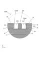
- FIG. 1 is a perspective view of a wiring board, an electronic component mounting package, and an electronic module according to a first embodiment of the present disclosure
- FIG. 2 is an enlarged view of a main portion A in the wiring board shown in FIG. 1
- FIG. FIG. 2 is a plan view of a main portion A of the wiring board shown in FIG. 1
- 4 is an X1-X1 cross-sectional view of the main portion A in the wiring board shown in FIG. 3
- FIG. FIG. 10 is a plan view of a main part A of a wiring board according to a second embodiment of the present disclosure
- 6 is an X2-X2 cross-sectional view of the main portion A in the wiring board shown in FIG. 5;
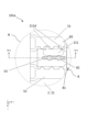
- FIG. 1 is a schematic perspective view of an electronic component mounting package and an electronic module according to a first embodiment to which an external substrate is connected;
- FIG. FIG. 8 is a plan perspective view of a main portion B in the wiring board shown in FIG. 7; 4 is a plan view of an external substrate; FIG. It is the top view seen from the back surface of an external substrate.
- FIG. 9 is a Y1-Y1 cross-sectional view of a main portion B in the wiring board shown in FIG. 8;
- the wiring substrate, the electronic component mounting package using the wiring substrate, and the electronic module may be oriented upward or downward, but for convenience, an orthogonal coordinate system xyz is defined, and the z direction The positive side of is the upper side.
- the direction in which the signal line extends refers to, for example, the x direction in the drawings.
- the direction perpendicular to the extending direction of the signal line refers to, for example, the y direction in the drawings.
- planar view is a concept that includes planar perspective.
- FIG. 1 A wiring board 101a according to a first embodiment of the present disclosure will be described with reference to FIGS. 1 to 4.
- FIG. The wiring board 101 a includes at least a first insulating layer 1 , a second insulating layer 2 , a signal line 53 and a first ground conductor line 51 .
- the wiring board 101 a may further include a second ground conductor line 52 , a third insulating layer 3 , and a ground conductor layer 6 .
- an external substrate 8 such as a flexible substrate (FPC: Flexible Printed Circuits) may be connected to the wiring substrate 101a.
- FPC Flexible Printed Circuits
- the first insulating layer 1 has a first upper surface 11 and a first lower surface 12, as shown in FIG.
- materials for the first insulating layer 1 include ceramic materials such as aluminum oxide sintered bodies, mullite sintered bodies, silicon carbide sintered bodies, aluminum nitride sintered bodies, and silicon nitride sintered bodies; Dielectric materials such as glass-ceramic materials can be used.
- the first insulating layer 1 may have a structure in which a plurality of insulating layers are laminated.
- the first insulating layer 1 has, for example, a rectangular shape in plan view, a size of 4 mm ⁇ 4 mm to 50 mm ⁇ 50 mm, and a thickness of 0.5 mm to 10 mm.
- the second insulating layer 2 has, as shown in FIG. there is A second insulating layer 2 is located on the first insulating layer 1 .
- the material of the second insulating layer 2 may be the same as or different from the material of the first insulating layer 1, and for example, the same material as that of the first insulating layer 1 described above can be used.
- the second insulating layer 2 may have a structure in which a plurality of insulating layers are laminated.
- the second insulating layer 2 has, for example, a rectangular shape in plan view, a size of 4 mm ⁇ 4 mm to 50 mm ⁇ 50 mm, and a thickness of 0.5 mm to 10 mm.
- the signal line 53 is located on the second upper surface 21 of the second insulating layer 2, as shown in FIGS. 2 to 4, and extends in the x direction in this embodiment.
- the direction in which the signal lines extend will be referred to as the x-direction
- the direction orthogonal to the direction in which the signal lines will extend will be referred to as the y-direction.
- materials for the signal line 53 include metal materials such as gold, silver, copper, nickel, tungsten, molybdenum, and manganese.
- the signal line 53 may be formed by sintering a metal paste on the second upper surface 21, or may be formed using a thin film forming technique such as a vapor deposition method or a sputtering method.
- the surface of the signal line 53 may be plated with a metal such as nickel plating or gold plating.
- the signal line 53 has a width of 0.05 mm to 2 mm and a length of 1.5 mm to 25 mm, for example.
- the thickness of the signal line 53 is, for example, 0.01 to 0.1 mm.
- the width, length, and thickness of the signal line 53 referred to here can be defined as the dimension in the y direction, the dimension in the x direction, and the dimension in the z direction, respectively.
- the width/length/thickness of the first ground conductor line 51, the second ground conductor line 52, and the third ground conductor line 83, which will be described later, can be similarly defined.
- the first ground conductor line 51 is positioned on the second upper surface 21 of the second insulating layer 2 with a first spacing L1 in the y direction from the signal line 53, It extends along the signal line 53 .
- the first ground conductor line 51 extends parallel to the signal line 53 and extends in the x direction.
- the material of the first ground conductor line 51 may be the same as or different from the material of the signal line 53, and examples thereof include the same material as the material of the signal line 53 described above.
- the first ground conductor line 51 may be formed by a method similar to that of the signal line 53 described above.
- the first ground conductor line 51 has a width of 0.05 mm to 2 mm and a length of 1.5 mm to 25 mm, for example.
- the thickness of the first ground conductor line 51 is, for example, 0.01 mm to 0.1 mm.
- the dimension of the first interval L1 is, for example, 0.1 mm to 1 mm.
- wiring board 101a may have a GSG structure, that is, a single-ended signal line.
- the second insulating layer 2 has the first opening 211 opening in the second upper surface 21 .
- at least one first opening 211 is located between the signal line 53 and the first ground conductor line 51 and is in contact with the first ground conductor line 51 in plan view.
- the first opening 211 is filled with air or a dielectric material such as a resin material or a glass material, and has a lower dielectric constant than the first insulating layer 1 and the second insulating layer 2 .
- the first opening 211 Since the first opening 211 is in contact with the first ground conductor line 51, the first opening 211 can be provided as large as possible.
- the member F can escape into the first opening 211 . Therefore, compared to the case where the first opening 211 is not in contact with the first ground conductor line 51, the amount of the joint member F can be increased, and the joint strength with the lead terminals and the external substrate 8 can be improved.
- the joining member F may be any member as long as it electrically connects the lead terminal or the external substrate 8 and the first ground conductor line 51, and examples thereof include solder.
- the second insulating layer 2 has the first opening 211 in contact with the first ground conductor line 51 , the opening 211 located between the signal line 53 and the first ground conductor line 51 in plan view can be used.
- the second insulating layer 2 having a high dielectric constant can be reduced, and the drop in impedance in the signal line 53 can be reduced. Therefore, by using the wiring substrate 101a, it is possible to provide an electronic component mounting package and an electronic module capable of reducing loss in transmission of high-frequency signals.
- the first spacing L1 becomes narrower, and the impedance value tends to decrease.
- the first opening 211 can be provided as large as possible, thereby reducing the impedance drop and miniaturizing the wiring board 101a. can do.
- the first opening 211 may be positioned with a second distance L2 from the signal line 53 in the y direction.
- the dimension of the second interval L2 is, for example, 0.01 mm to 0.5 mm.
- the first opening 211 may penetrate from the second upper surface 21 to the second lower surface 22 as shown in FIG. That is, the first opening 211 may penetrate through the second insulating layer 2 .
- the first opening 211 is an oblong portion including, for example, a first arcuate portion 211b, a second arcuate portion 211c, and a first linear portion 211a in plan view. good too.
- the first opening 211 has a width of 0.1 mm to 1 mm and a dimension (depth) in the z direction of 0.5 mm to 10 mm. Depending on the shape of the first opening 211, the width and depth of the first opening 211 may not be constant.
- the first opening 211 may have an elliptical shape, a square shape, or a rectangular shape with rounded corners in plan view. Also, the first opening 211 may extend to the end (end face) of the second insulating layer 2 . In other words, the first opening 211 may have a shape in which the end (end face) of the second insulating layer 2 is notched.
- the third insulating layer 3 may be positioned on the second insulating layer 2.
- the material of the third insulating layer 3 may be the same as or different from the material of the first insulating layer 1, and for example, the same material as that of the first insulating layer 1 described above can be used.
- the first opening 211 may be positioned with a sixth gap L211 in the x direction from the third insulating layer 3 .
- the dimension of the sixth interval L211 is, for example, 0.01 mm to 0.5 mm.
- the first opening 211 has a first concave portion 211d located on the inner peripheral surface of the first opening 211 and in contact with the first ground conductor line 51. good too.
- the first ground conductor line 51 is positioned continuously with the first ground conductor line 51 on the inner peripheral surface of the first recess 211d.
- 1 ground conductor film 511 may be provided. That is, the first concave portion 211d and the first ground conductor film 511 may form a so-called castellation.
- the first concave portion 211d has a semi-elliptical shape in plan view, but the shape of the first concave portion 211d is not limited to this, and may be a square shape or a rectangular shape with rounded corners. may
- the second insulating layer 2 may be exposed on the inner peripheral surface of the first opening 211 excluding the first recess 211d.
- conductors such as the first ground conductor film 511 may not be provided on the inner peripheral surface of the first opening 211 excluding the first recess 211d.
- the impedance value between the signal line 53 and the first ground conductor line 51 is reduced, and an increase in signal loss can be reduced.
- the signal line 53 is provided on the second insulating layer 2 by screen printing or the like, a portion of the signal line 53 may be positioned on a portion of the inner peripheral surface of the first opening 211 due to positional deviation. In such a case, the possibility of short-circuiting can be reduced.
- the inner peripheral surface of the first opening 211 referred to here is a surface perpendicular to the y direction in the present embodiment.
- the first opening 211 may have a plurality of first recesses 211d positioned at fifth intervals L5 in the x direction, and the fifth intervals L5 are transmitted through the signal line 53. It may be 1/2 or less of the signal wavelength ⁇ . With such a configuration, the signal transmission characteristics can be effectively improved. Furthermore, when the fifth interval L5 is equal to or less than 1/4 of the signal wavelength ⁇ transmitted through the signal line 53, the ground potential is further strengthened, and the signal transmission characteristics can be effectively improved.
- the shapes of the plurality of first recesses 211d may be the same or different.
- the same metal pins are used when forming the first recesses 211d by mechanical punching using metal pins. Since it can be used, manufacturing of the wiring substrate 101a can be facilitated. If the shapes of the plurality of first concave portions 211d are different from each other, the degree of freedom in manufacturing is improved. It becomes possible to strengthen the electric potential.
- the first opening 211 may be an oblong portion including the first arcuate portion 211b, the second arcuate portion 211c, and the first linear portion 211a.
- at least one of the plurality of first recesses 211d is located between the first arcuate portion 211b and the first linear portion 211a and/or between the second arcuate portion 211c and the first linear portion 211a. may be located in According to such a configuration, for example, even when the wiring board 101a is miniaturized, the number of the first concave portions 211d can be increased while maintaining the fifth interval L5. As a result, the ground potential is further strengthened, and the possibility of occurrence of crosstalk and resonance due to the spread of the electric field distribution beyond the desired range during transmission of high frequency signals can be reduced.
- the second spacing L2 may be equal to or less than the width W211 of the first opening 211 in the y direction.
- the first opening 211 can be provided as large as possible while reducing the possibility of damage to the signal line 53 due to positional deviation in punching. As a result, it is possible to reduce the possibility that the impedance value will decrease, and the possibility of signal loss in the signal line 53 can be reduced.
- the first spacing L1 may be equal to or greater than the width W53 of the signal line 53 . In this case, since the width W53 of the signal line 53 can be made small, it is possible to reduce the decrease in the impedance value when the lead terminal or the external substrate 8 is connected.
- the width W53 of the signal line 53 may be equal to or less than the width W211 of the first opening 211 in the y direction. Furthermore, the width W211 of the first opening 211 may be larger than the width W53 of the signal line 53 and smaller than the width W51 of the first ground conductor line 51 in the y direction. In the wiring substrate 101a, when miniaturization is not required, the width W51 of the first ground conductor line 51 is shorter than the width W211 of the first opening 211 and longer than the width W53 of the signal line 53. good too. With such a configuration, even when the first distance L1 is large, the first opening 211 located between the first ground conductor line 51 and the signal line 53 in plan view can be provided as large as possible. .
- the second insulating layer 2 with a high dielectric constant which is positioned between the first ground conductor line 51 and the signal line 53 in a plan view, can be reduced as much as possible, effectively reducing the drop in impedance. be able to.
- the wiring board 101a may further include the second ground conductor line 52 and the ground conductor layer 6 as described above.
- the second ground conductor line 52 is located on the second upper surface 21 of the second insulating layer 2 with a third spacing L3 in the y direction from the signal line 53, It extends along the line 53 .
- the material of the second ground conductor line 52 may be the same as or different from that of the signal line 53, and examples thereof include materials similar to those of the signal line 53 described above.
- the second ground conductor line 52 may be formed by the same method as the signal line 53 described above.
- the second ground conductor line 52 has a width of 0.05 mm to 2 mm and a length of 1.5 mm to 25 mm, for example.
- the thickness of the second ground conductor line 52 is, for example, 0.01 to 0.1 mm.
- the wiring board 101a When the wiring board 101a is provided with the second ground conductor line 52, the signal transmission loss that occurs when the wiring such as the signal line 53 and the first ground conductor line 51 is bent (curved portion) is reduced. be able to. In addition, it is possible to reduce the possibility of occurrence of crosstalk or resonance due to the spread of the electric field distribution beyond the desired range when transmitting the high frequency signal.
- the ground conductor layer 6 is located between the first insulating layer 1 and the second insulating layer 2 .
- the material of the ground conductor layer 6 is, for example, a metal material such as tungsten, molybdenum and manganese, and the surface thereof may be plated with nickel or gold. In this embodiment, as shown in FIG. 4 , the ground conductor layer 6 is exposed on the lower surface of the first opening 211 .
- the electrolytic coupling can be strengthened. Therefore, crosstalk and resonance caused by the spread of the electric field distribution beyond the desired range during the transmission of the high-frequency signal can be prevented. The possibility of occurrence can be reduced.
- the ground conductor layer 6 may be electrically connected to the first ground conductor line 51 by the first ground conductor film 511 described above. In this case, since the electrolytic coupling can be further strengthened, it is possible to effectively reduce the possibility of occurrence of crosstalk and resonance caused by the spread of the electric field distribution beyond the desired range when transmitting high-frequency signals. can be done.
- an insulating film made of ceramic (for example, alumina coat) or resin is located on part of the first ground conductor line 51, the second ground conductor line 52, and the signal line 53.
- the insulating film can be provided on the first ground conductor line 51 and the signal line 53 by screen printing. Also, the insulating film may be positioned only on the signal line 53 . With such a configuration, it is possible to reduce the possibility that the first ground conductor line 51, the second ground conductor line 52, and the signal line 53 are short-circuited.
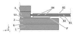
- An external substrate 8 may be connected to the electronic component mounting package 100 including the wiring substrate 101a, as shown in FIG. Note that FIG. 7 is a transparent view of a portion of the wiring substrate 101a where the external substrate 8 is overlapped.
- the external substrate 8 has an insulating substrate 81 , a signal transmission line 82 and a third ground conductor line 83 .
- the third ground conductor line 83 and the signal transmission line 82 are located on the insulating substrate 81 , that is, on the upper and lower surfaces of the insulating substrate 81 . More specifically, as shown in FIG.
- the third ground conductor line 83 is located across the upper and lower surfaces of the insulating substrate 81, and the connecting conductor 84 connects the third ground conductors located on the upper and lower surfaces.
- the conductor lines 83 are electrically connected.
- the signal transmission line 82 is also positioned across the upper and lower surfaces of the insulating substrate 81 similarly to the third ground conductor line 83 , and the signal transmission line 82 positioned on the upper and lower surfaces is electrically connected by the connection conductor 84 . It is connected.
- the signal transmission line 82 of the external substrate 8 is connected to the signal line 53 of the wiring board 101a via the joint member F.
- the third ground conductor line 83 is connected to the first ground conductor line 51 and the second ground conductor line 52 of the wiring board 101a via the joint member F. As shown in FIG.
- the third ground conductor line 83 overlaps at least a portion of the first recess 211d.
- the joint member F that overflows excessively is removed. F can also escape into the first recess 211d. As a result, the bonding strength with the lead terminals and the external substrate 8 can be further improved.
- lead terminals may be connected to the wiring substrate 101a.
- the lead terminal can be connected to each of the signal line 53, the first ground conductor line 51, and the second ground conductor line 52 via the joint member F.
- FIG. 5 a wiring board 101b according to a second embodiment of the present disclosure will be described with reference to FIGS. 5 and 6.
- FIG. 5 only the configuration of the second embodiment that differs from the configuration of the first embodiment will be described, and the configuration other than that will be given the same reference numerals as in the first embodiment, and the description thereof will be omitted. .
- a wiring substrate 101b according to the second embodiment differs from the first embodiment in that the second insulating layer 2 further has a second opening 212 .
- the second insulating layer 2 further has one or more second openings 212 opening in the second upper surface 21, as shown in FIGS. At least one second opening 212 is located between the signal line 53 and the second ground conductor line 52 and is in contact with the second ground conductor line 52 in plan view.
- the second opening 212 is filled with air or a dielectric material such as a resin material or a glass material, and has a lower dielectric constant than the first insulating layer 1 and the second insulating layer 2 .
- the second insulating layer 2 has the second opening 212 in contact with the second ground conductor line 52 , it has the first opening 211 in contact with the first ground conductor line 51 .
- the same effect as in the case can be obtained. Therefore, by using the wiring board 101b, it is possible to provide an electronic component mounting package and an electronic module capable of reducing loss in transmission of high-frequency signals.
- the second opening 212 may be positioned with a fourth distance L4 from the signal line 53 in the y direction.
- the dimension of the fourth spacing L4 is, for example, 0.05 mm to 0.5 mm, and may be the same as or different from the second spacing L2.
- the fourth spacing L4 and the second spacing L2 are the same, the second insulating layer 2 sandwiching the signal line 53 has the same thickness in the y direction, which facilitates adjustment of the impedance value. can be done.
- the second opening 212 may penetrate from the second upper surface 21 to the second lower surface 22 as shown in FIG. That is, the second opening 212 may penetrate through the second insulating layer 2 .
- the second opening 212 may have the same shape as the first opening 211 .
- the width is 0.1 mm to 1 mm and the dimension (depth) in the z direction is 0.5 mm to 10 mm.
- the width and depth of the second opening 212 referred to here need not be constant across the entirety of the second opening 212 , like the first opening 211 .
- the second opening 212 may extend to the end (end surface) of the second insulating layer 2 . In other words, the second opening 212 may have a shape in which the end (end surface) of the second insulating layer 2 is notched.
- the second opening 212 may have an elliptical shape, a square shape, or a rectangular shape with rounded corners in plan view. Also, the second opening 212 does not necessarily have to have the same shape and size as the first opening 211 . In the present embodiment, the second openings 212 are symmetrically positioned across the signal line 53, but the shape, position, and size of the second openings 212 are not limited to this. That is, the sizes of the first opening 211 and the second opening 212 may be different, and the second opening 212 can be appropriately provided at a position where a reduction in impedance is required.
- the impedance values can be made equal on both sides of the signal line 53 . , can facilitate adjustment of the impedance value.
- the second opening 212 may have a second recess 212d, similar to the first recess 211d of the first opening 211, as shown in FIGS.
- the second ground conductor line 52 is positioned continuously with the second ground conductor line 52 on the inner peripheral surface of the second recess 212d.
- 2 may have a ground conductor film 521 .
- the second concave portion 212d has a semi-elliptical shape in plan view, but may have a square shape or a rectangular shape with rounded corners.
- the shape of the second recess 212d may be the same as or different from that of the first recess 211d described above.
- the second opening 212 may have a plurality of second recesses 212d positioned at seventh intervals L7 in the x direction, and the seventh intervals L7 are transmitted through the signal line 53. It may be 1/2 or less of the signal wavelength ⁇ . With such a configuration, it is possible to obtain the same effect as when the first recesses 211d are positioned with the fifth interval L5 therebetween.
- the second opening 212 is an elliptical portion including an arcuate portion and a linear portion in a plan view
- at least one of the plurality of second recesses 212d is formed by the arcuate portion and the linear portion. may be located in between.
- the wiring board 101b is miniaturized, the same effect as when the first opening 211 has a plurality of first recesses 211d can be obtained.
- the size and positional relationship of the first ground conductor line 51, the signal line 53, and the first opening 211 may be A similar one can be adopted. Accordingly, effects similar to those of the first ground conductor line 51, the signal line 53, and the first opening 211 can be obtained. It should be noted that the above-mentioned first interval L1 can be read as the third interval L3, and the second interval L2 can be read as the fourth interval L4.
- Method for manufacturing the wiring board 101a according to the first embodiment of the present disclosure will be described. Note that the method for manufacturing the wiring board 101a according to the embodiment of the present disclosure is not limited to the following embodiments, and may be manufactured using a 3D printer, for example.
- a plurality of green sheets are formed. Specifically, for example, ceramic powder such as boron nitride, aluminum nitride, silicon nitride, silicon carbide, or beryllium oxide is added and mixed with an organic binder, a plasticizer, a solvent, or the like to obtain a mixture, and the mixture is formed into a layer. to produce a plurality of green sheets. Next, the plurality of green sheets described above are processed by a mold or the like to prepare a plurality of green sheets formed in the outer shapes of the first insulating layer 1 and the second insulating layer 2 in plan view.
- ceramic powder such as boron nitride, aluminum nitride, silicon nitride, silicon carbide, or beryllium oxide is added and mixed with an organic binder, a plasticizer, a solvent, or the like to obtain a mixture, and the mixture is formed into a layer.
- the plurality of green sheets described above are processed by a mold or the like to prepare a
- a green sheet formed in the outer shape of the third insulating layer 3 is additionally prepared.
- a first opening 211 is formed in the green sheet that will become the second insulating layer 2 using a mold, laser, or the like.
- the green sheet serving as the second insulating layer 2 is provided with the first concave portion 211d in the same manner as the first opening portion 211.
- FIG. When the second insulating layer 2 has the second opening 212 as in the second embodiment, it can be provided by the same method as the first opening 211 .
- a high-melting-point metal powder such as tungsten or molybdenum is prepared, and an organic binder, plasticizer, solvent, or the like is added and mixed to prepare a metal paste.
- a metal paste is printed in a predetermined pattern on a plurality of green sheets formed in the outer shape of each of the first insulating layer 1, the second insulating layer 2, and the third insulating layer 3, and the signal line 53 and the first ground are printed.
- a conductor line 51 and a second ground conductor line 52 are formed.
- the metal paste may contain glass or ceramics in order to increase the bonding strength with each insulating layer.
- the first ground conductor film 511 can be formed by printing a metal paste on the first concave portion 211d formed in the above-described process.
- the ground conductor layer 6 is made of a metallized layer made of a metal with a high melting point such as tungsten, molybdenum, or manganese, it can be formed as follows. That is, first, a metal paste prepared by kneading powder of a metal with a high melting point together with an organic solvent and a binder so as to be well mixed is used as the second lower surface 22 of the second insulating layer 2 or the first upper surface 11 of the first insulating layer 1. A predetermined portion of the ceramic green sheet is printed by a method such as screen printing.
- the electronic component mounting package 100 includes a wiring substrate 101a, a substrate 102, and a frame 103. As shown in FIG. The frame 103 is bonded to the upper surface of the substrate 102, and the wiring board 101a is fixed to the frame 103. As shown in FIG. Also, the wiring substrate 101 a may be bonded to the upper surface of the substrate 102 .
- the substrate 102 has an upper surface.
- the substrate 102 has, for example, a square shape in plan view, a size of 10 mm ⁇ 10 mm to 50 mm ⁇ 50 mm, and a thickness of 0.5 mm to 20 mm.
- Materials for the substrate 102 include, for example, metal materials such as copper, iron, tungsten, molybdenum, nickel, and cobalt, or alloys containing these metal materials.
- the substrate 102 may be a single metal plate or a laminate in which a plurality of metal plates are laminated.
- the material of the substrate 102 is the metal material described above, the surface of the substrate 102 is plated with nickel, gold, or the like using an electroplating method or an electroless plating method in order to reduce oxidation corrosion. Layers may be formed. Further, the material of the substrate 102 is an insulating material, such as aluminum oxide sintered body, mullite sintered body, silicon carbide sintered body, aluminum nitride sintered body, silicon nitride sintered body, or Ceramic materials such as glass ceramics may also be used.
- the frame 103 is located on the upper surface of the substrate 102 and protects the electronic components 104 located inside in plan view. That is, in plan view, frame 103 is positioned so as to surround electronic component 104 . As shown in FIG. 1, in this embodiment, the frame 103 is not positioned on one side of the outer edge of the upper surface of the substrate 102 . That is, the outer edge of the upper surface of the substrate 102 is surrounded by the frame 103 and the wiring substrate 101a. In other words, the electronic component 104 is surrounded by the frame 103 and the wiring substrate 101a. Thus, the frame 103 does not have to surround the entire outer edge of the upper surface of the substrate 102 . Further, in this embodiment, the frame 103 is positioned along the outer edge of the top surface of the substrate 102 , but the frame 103 may be positioned inside the outer edge of the top surface of the substrate 102 .
- the material of the frame 103 may be, for example, metal materials such as copper, iron, tungsten, molybdenum, nickel or cobalt, or alloys containing these metal materials.
- the material of the frame 103 is an insulating material, such as an aluminum oxide sintered body, a mullite sintered body, a silicon carbide sintered body, an aluminum nitride sintered body, and a silicon nitride sintered body.
- it may be a ceramic material such as glass ceramics.
- the frame 103 can be joined to the substrate 102 via brazing material or the like.
- the material of the brazing material is, for example, silver, copper, gold, aluminum or magnesium, and may contain additives such as nickel, cadmium or phosphorus.
- the electronic module 10 includes an electronic component mounting package 100 , an electronic component 104 , and a lid 106 .
- Electronic module 10 may also include a seal ring 105 .
- the electronic component 104 may be, for example, a component that performs signal processing such as converting an optical signal into an electrical signal or converting an electrical signal into an optical signal.
- the electronic component 104 is located on the upper surface of the substrate 102 and housed in the electronic component mounting package 100 .
- Examples of the electronic component 104 include a semiconductor laser (LD), an optical semiconductor element such as a photodiode (PD), a semiconductor integrated circuit element, and a sensor element such as an optical sensor.
- Electronic component 104 may be formed from a semiconductor material such as gallium arsenide or gallium nitride, for example.
- the lid 106 is positioned on the frame 103 to cover the inside of the electronic component mounting package 100 and protects the electronic component 104 together with the frame 103 .
- the lid body 106 has, for example, a square shape in plan view, a size of 10 mm ⁇ 10 mm to 50 mm ⁇ 50 mm, and a thickness of 0.5 mm to 2 mm.
- Materials for the lid 106 include, for example, metal materials such as iron, copper, nickel, chromium, cobalt, molybdenum, and tungsten, or alloys obtained by combining a plurality of these metal materials. By subjecting an ingot of such a metal material to a metal working method such as a rolling method or a punching method, the metal member that constitutes the lid 106 can be manufactured.
- the seal ring 105 has the function of joining the lid 106 and the frame 103 together.
- the seal ring 105 is positioned on the frame 103 and surrounds the electronic component 104 in plan view.
- Materials for the seal ring 105 include, for example, metal materials such as iron, copper, silver, nickel, chromium, cobalt, molybdenum, and tungsten, or alloys obtained by combining a plurality of these metal materials. If the seal ring 105 is not provided on the frame 103, the lid 106 may be bonded via a bonding material such as solder, brazing material, glass, or resin adhesive.
- the present disclosure can be used as a wiring board, an electronic component mounting package using the wiring board, and an electronic module.
- First insulating layer 11 First upper surface 12 First lower surface 2 Second insulating layer 21 Second upper surface 211 First opening 211a First linear portion 211b First arcuate portion 211c Second arcuate portion 211d First concave portion W211 First opening width 212 Second opening 212d Second recess W212 Second opening width 22 Second lower surface 23 Notch 3 Third insulating layer 51 First ground conductor line 511 First ground conductor film W51 First first ground conductor film W51 Width of ground conductor line 52 Second ground conductor line 521 Second ground conductor film W52 Width of second ground conductor line 53 Signal line W53 Width of signal line 6 Ground conductor layer 8 External substrate 81 Insulating substrate 82 Signal transmission line 83 Third Ground conductor line 84 Connection conductor L1 First interval L2 Second interval L3 Third interval L4 Fourth interval L5 Fifth interval L211 Sixth interval L7 Seventh interval F Joint member 10 Electronic module 100 Packages for mounting electronic parts 101a-b Wiring Substrate 102 Substrate 103 Frame 104 Electronic component
Landscapes
- Engineering & Computer Science (AREA)
- Microelectronics & Electronic Packaging (AREA)
- Structure Of Printed Boards (AREA)
Priority Applications (3)
| Application Number | Priority Date | Filing Date | Title |
|---|---|---|---|
| CN202380018332.XA CN118613907A (zh) | 2022-01-28 | 2023-01-20 | 布线基板、使用了布线基板的电子部件安装用封装体及电子模块 |
| JP2023576876A JP7753403B2 (ja) | 2022-01-28 | 2023-01-20 | 配線基板、配線基板を用いた電子部品実装用パッケージ、および電子モジュール |
| US18/832,975 US20250151200A1 (en) | 2022-01-28 | 2023-01-20 | Wiring board, electronic component mounting package using wiring board, and electronic module |
Applications Claiming Priority (2)
| Application Number | Priority Date | Filing Date | Title |
|---|---|---|---|
| JP2022012043 | 2022-01-28 | ||
| JP2022-012043 | 2022-01-28 |
Publications (1)
| Publication Number | Publication Date |
|---|---|
| WO2023145651A1 true WO2023145651A1 (ja) | 2023-08-03 |
Family
ID=87471877
Family Applications (1)
| Application Number | Title | Priority Date | Filing Date |
|---|---|---|---|
| PCT/JP2023/001745 Ceased WO2023145651A1 (ja) | 2022-01-28 | 2023-01-20 | 配線基板、配線基板を用いた電子部品実装用パッケージ、および電子モジュール |
Country Status (4)
| Country | Link |
|---|---|
| US (1) | US20250151200A1 (https=) |
| JP (1) | JP7753403B2 (https=) |
| CN (1) | CN118613907A (https=) |
| WO (1) | WO2023145651A1 (https=) |
Cited By (3)
| Publication number | Priority date | Publication date | Assignee | Title |
|---|---|---|---|---|
| WO2025063160A1 (ja) * | 2023-09-19 | 2025-03-27 | 京セラ株式会社 | 配線構造体および電子モジュール |
| WO2025070079A1 (ja) * | 2023-09-29 | 2025-04-03 | 京セラ株式会社 | 配線基板および電子モジュール |
| WO2025225641A1 (ja) * | 2024-04-25 | 2025-10-30 | 京セラ株式会社 | 配線基板、パッケージ及び光モジュール |
Families Citing this family (1)
| Publication number | Priority date | Publication date | Assignee | Title |
|---|---|---|---|---|
| US20240027493A1 (en) * | 2020-11-27 | 2024-01-25 | Kyocera Corporation | Wiring board and probe card |
Citations (4)
| Publication number | Priority date | Publication date | Assignee | Title |
|---|---|---|---|---|
| WO2016186128A1 (ja) * | 2015-05-20 | 2016-11-24 | 京セラ株式会社 | 半導体素子パッケージ、半導体装置および実装構造体 |
| WO2018074100A1 (ja) * | 2016-10-21 | 2018-04-26 | 京セラ株式会社 | 高周波基体、高周波パッケージおよび高周波モジュール |
| JP2019114689A (ja) * | 2017-12-25 | 2019-07-11 | 京セラ株式会社 | 高周波基体、高周波パッケージおよび高周波モジュール |
| WO2020179937A1 (ja) * | 2019-03-07 | 2020-09-10 | 京セラ株式会社 | 配線基板、電子部品用パッケージおよび電子装置 |
-
2023
- 2023-01-20 CN CN202380018332.XA patent/CN118613907A/zh active Pending
- 2023-01-20 US US18/832,975 patent/US20250151200A1/en active Pending
- 2023-01-20 JP JP2023576876A patent/JP7753403B2/ja active Active
- 2023-01-20 WO PCT/JP2023/001745 patent/WO2023145651A1/ja not_active Ceased
Patent Citations (4)
| Publication number | Priority date | Publication date | Assignee | Title |
|---|---|---|---|---|
| WO2016186128A1 (ja) * | 2015-05-20 | 2016-11-24 | 京セラ株式会社 | 半導体素子パッケージ、半導体装置および実装構造体 |
| WO2018074100A1 (ja) * | 2016-10-21 | 2018-04-26 | 京セラ株式会社 | 高周波基体、高周波パッケージおよび高周波モジュール |
| JP2019114689A (ja) * | 2017-12-25 | 2019-07-11 | 京セラ株式会社 | 高周波基体、高周波パッケージおよび高周波モジュール |
| WO2020179937A1 (ja) * | 2019-03-07 | 2020-09-10 | 京セラ株式会社 | 配線基板、電子部品用パッケージおよび電子装置 |
Cited By (3)
| Publication number | Priority date | Publication date | Assignee | Title |
|---|---|---|---|---|
| WO2025063160A1 (ja) * | 2023-09-19 | 2025-03-27 | 京セラ株式会社 | 配線構造体および電子モジュール |
| WO2025070079A1 (ja) * | 2023-09-29 | 2025-04-03 | 京セラ株式会社 | 配線基板および電子モジュール |
| WO2025225641A1 (ja) * | 2024-04-25 | 2025-10-30 | 京セラ株式会社 | 配線基板、パッケージ及び光モジュール |
Also Published As
| Publication number | Publication date |
|---|---|
| JPWO2023145651A1 (https=) | 2023-08-03 |
| JP7753403B2 (ja) | 2025-10-14 |
| US20250151200A1 (en) | 2025-05-08 |
| CN118613907A (zh) | 2024-09-06 |
Similar Documents
| Publication | Publication Date | Title |
|---|---|---|
| WO2023145651A1 (ja) | 配線基板、配線基板を用いた電子部品実装用パッケージ、および電子モジュール | |
| EP2237316B1 (en) | Connection terminal, package using the same and electronic device | |
| JP7753391B2 (ja) | 配線基板、配線基板を用いた電子部品実装用パッケージ、および電子モジュール | |
| JP6777755B2 (ja) | 高周波基体、高周波パッケージおよび高周波モジュール | |
| US20240405130A1 (en) | Wiring board, electronic component package, and electronic apparatus | |
| JP7021041B2 (ja) | 配線基板、電子部品パッケージおよび電子装置 | |
| US6936921B2 (en) | High-frequency package | |
| US20250351264A1 (en) | Wiring board, electronic component mounting package using wiring board, and electronic module | |
| JP7432703B2 (ja) | 配線基体および電子装置 | |
| JP7230251B2 (ja) | 配線基板、電子部品パッケージおよび電子装置 | |
| KR102463392B1 (ko) | 배선 기체, 전자부품 수납용 패키지 및 전자장치 | |
| JP7817435B2 (ja) | 配線基板、配線基板を用いた電子部品実装用パッケージ、および電子モジュール | |
| EP4550567A1 (en) | Waveguide converter, package for mounting electronic component, and waveguide conversion device | |
| US20240105600A1 (en) | Wiring substrate, wiring structure using wiring substrate, electronic component mounting package, and electronic module | |
| JP7254011B2 (ja) | 配線基体、半導体素子収納用パッケージ、および半導体装置 | |
| JP7784549B2 (ja) | 配線構造体および電子モジュール | |
| JP7206418B2 (ja) | 配線基体、半導体素子収納用パッケージ、および半導体装置 | |
| JP2001230342A (ja) | 高周波回路部品搭載用基板の実装構造 | |
| WO2024122576A1 (ja) | 配線基板、配線基板を用いた電子部品実装用パッケージ、および電子モジュール | |
| WO2024029628A1 (ja) | 配線基板、配線基板を用いた電子部品実装用パッケージおよび電子モジュール | |
| WO2026048794A1 (ja) | 配線基板、電子部品収納用パッケージ及び電子モジュール | |
| JP2024104570A (ja) | 配線構造体、配線構造体を用いた電子部品実装用パッケージ、および電子モジュール | |
| JP2021120985A (ja) | 配線基体および電子装置 | |
| JP2004055570A (ja) | 高周波用パッケージ | |
| CN113748505A (zh) | 布线基板、电子部件用封装件及电子装置 |
Legal Events
| Date | Code | Title | Description |
|---|---|---|---|
| 121 | Ep: the epo has been informed by wipo that ep was designated in this application |
Ref document number: 23746864 Country of ref document: EP Kind code of ref document: A1 |
|
| ENP | Entry into the national phase |
Ref document number: 2023576876 Country of ref document: JP Kind code of ref document: A |
|
| WWE | Wipo information: entry into national phase |
Ref document number: 202380018332.X Country of ref document: CN |
|
| WWE | Wipo information: entry into national phase |
Ref document number: 18832975 Country of ref document: US |
|
| NENP | Non-entry into the national phase |
Ref country code: DE |
|
| 122 | Ep: pct application non-entry in european phase |
Ref document number: 23746864 Country of ref document: EP Kind code of ref document: A1 |
|
| WWP | Wipo information: published in national office |
Ref document number: 18832975 Country of ref document: US |