WO2023145441A1 - 光検出装置 - Google Patents
光検出装置 Download PDFInfo
- Publication number
- WO2023145441A1 WO2023145441A1 PCT/JP2023/000519 JP2023000519W WO2023145441A1 WO 2023145441 A1 WO2023145441 A1 WO 2023145441A1 JP 2023000519 W JP2023000519 W JP 2023000519W WO 2023145441 A1 WO2023145441 A1 WO 2023145441A1
- Authority
- WO
- WIPO (PCT)
- Prior art keywords
- pixel
- substrate
- semiconductor substrate
- film
- dielectric multilayer
- Prior art date
- Legal status (The legal status is an assumption and is not a legal conclusion. Google has not performed a legal analysis and makes no representation as to the accuracy of the status listed.)
- Ceased
Links
Images











Classifications
-
- H—ELECTRICITY
- H10—SEMICONDUCTOR DEVICES; ELECTRIC SOLID-STATE DEVICES NOT OTHERWISE PROVIDED FOR
- H10F—INORGANIC SEMICONDUCTOR DEVICES SENSITIVE TO INFRARED RADIATION, LIGHT, ELECTROMAGNETIC RADIATION OF SHORTER WAVELENGTH OR CORPUSCULAR RADIATION
- H10F39/00—Integrated devices, or assemblies of multiple devices, comprising at least one element covered by group H10F30/00, e.g. radiation detectors comprising photodiode arrays
- H10F39/80—Constructional details of image sensors
- H10F39/809—Constructional details of image sensors of hybrid image sensors
-
- H—ELECTRICITY
- H10—SEMICONDUCTOR DEVICES; ELECTRIC SOLID-STATE DEVICES NOT OTHERWISE PROVIDED FOR
- H10F—INORGANIC SEMICONDUCTOR DEVICES SENSITIVE TO INFRARED RADIATION, LIGHT, ELECTROMAGNETIC RADIATION OF SHORTER WAVELENGTH OR CORPUSCULAR RADIATION
- H10F39/00—Integrated devices, or assemblies of multiple devices, comprising at least one element covered by group H10F30/00, e.g. radiation detectors comprising photodiode arrays
- H10F39/80—Constructional details of image sensors
- H10F39/805—Coatings
- H10F39/8057—Optical shielding
-
- H—ELECTRICITY
- H04—ELECTRIC COMMUNICATION TECHNIQUE
- H04N—PICTORIAL COMMUNICATION, e.g. TELEVISION
- H04N25/00—Circuitry of solid-state image sensors [SSIS]; Control thereof
- H04N25/70—SSIS architectures; Circuits associated therewith
- H04N25/79—Arrangements of circuitry being divided between different or multiple substrates, chips or circuit boards, e.g. stacked image sensors
-
- H—ELECTRICITY
- H10—SEMICONDUCTOR DEVICES; ELECTRIC SOLID-STATE DEVICES NOT OTHERWISE PROVIDED FOR
- H10F—INORGANIC SEMICONDUCTOR DEVICES SENSITIVE TO INFRARED RADIATION, LIGHT, ELECTROMAGNETIC RADIATION OF SHORTER WAVELENGTH OR CORPUSCULAR RADIATION
- H10F39/00—Integrated devices, or assemblies of multiple devices, comprising at least one element covered by group H10F30/00, e.g. radiation detectors comprising photodiode arrays
- H10F39/10—Integrated devices
- H10F39/12—Image sensors
- H10F39/18—Complementary metal-oxide-semiconductor [CMOS] image sensors; Photodiode array image sensors
- H10F39/182—Colour image sensors
-
- H—ELECTRICITY
- H10—SEMICONDUCTOR DEVICES; ELECTRIC SOLID-STATE DEVICES NOT OTHERWISE PROVIDED FOR
- H10F—INORGANIC SEMICONDUCTOR DEVICES SENSITIVE TO INFRARED RADIATION, LIGHT, ELECTROMAGNETIC RADIATION OF SHORTER WAVELENGTH OR CORPUSCULAR RADIATION
- H10F39/00—Integrated devices, or assemblies of multiple devices, comprising at least one element covered by group H10F30/00, e.g. radiation detectors comprising photodiode arrays
- H10F39/80—Constructional details of image sensors
- H10F39/806—Optical elements or arrangements associated with the image sensors
-
- H—ELECTRICITY
- H10—SEMICONDUCTOR DEVICES; ELECTRIC SOLID-STATE DEVICES NOT OTHERWISE PROVIDED FOR
- H10F—INORGANIC SEMICONDUCTOR DEVICES SENSITIVE TO INFRARED RADIATION, LIGHT, ELECTROMAGNETIC RADIATION OF SHORTER WAVELENGTH OR CORPUSCULAR RADIATION
- H10F39/00—Integrated devices, or assemblies of multiple devices, comprising at least one element covered by group H10F30/00, e.g. radiation detectors comprising photodiode arrays
- H10F39/80—Constructional details of image sensors
- H10F39/811—Interconnections
-
- H—ELECTRICITY
- H10—SEMICONDUCTOR DEVICES; ELECTRIC SOLID-STATE DEVICES NOT OTHERWISE PROVIDED FOR
- H10F—INORGANIC SEMICONDUCTOR DEVICES SENSITIVE TO INFRARED RADIATION, LIGHT, ELECTROMAGNETIC RADIATION OF SHORTER WAVELENGTH OR CORPUSCULAR RADIATION
- H10F39/00—Integrated devices, or assemblies of multiple devices, comprising at least one element covered by group H10F30/00, e.g. radiation detectors comprising photodiode arrays
- H10F39/011—Manufacture or treatment of image sensors covered by group H10F39/12
- H10F39/014—Manufacture or treatment of image sensors covered by group H10F39/12 of CMOS image sensors
-
- H—ELECTRICITY
- H10—SEMICONDUCTOR DEVICES; ELECTRIC SOLID-STATE DEVICES NOT OTHERWISE PROVIDED FOR
- H10F—INORGANIC SEMICONDUCTOR DEVICES SENSITIVE TO INFRARED RADIATION, LIGHT, ELECTROMAGNETIC RADIATION OF SHORTER WAVELENGTH OR CORPUSCULAR RADIATION
- H10F39/00—Integrated devices, or assemblies of multiple devices, comprising at least one element covered by group H10F30/00, e.g. radiation detectors comprising photodiode arrays
- H10F39/10—Integrated devices
- H10F39/12—Image sensors
- H10F39/199—Back-illuminated image sensors
Definitions
- the present disclosure relates to a photodetector, and more particularly to a photodetector that achieves both a shielding effect and heat resistance to a second-story pixel substrate and that can suppress parasitic photosensitivity in the second-story pixel substrate.
- Patent Document 1 reports a structure that suppresses the propagation of electromagnetic waves and heat between elements formed on the upper and lower substrates in a CMOS image sensor in which multiple substrates are stacked, thereby suppressing deterioration of the characteristics of the elements.
- Patent Document 1 a structure having a shield layer containing a conductive material between element layers, parasitics in a substrate that does not have a photoelectric conversion unit (hereinafter referred to as a second-level pixel substrate) It is disclosed that the photosensitivity (PLS) suppression and other electromagnetic noise propagation can be suppressed.
- PLS photosensitivity
- the structure in which a micro-sized structure with a high refractive index is provided in the insulating layer the total reflection of light at the interface between the structure and the insulating layer extends the optical path length and attenuates the light, resulting in parasitic It is disclosed that the photosensitivity can be suppressed.
- a structure using a dielectric film having a refractive index intermediate between that of the insulating layer and that of the silicon substrate as an antireflection portion can suppress color mixture noise due to reflection on the silicon substrate.
- the present disclosure has been made in view of such a situation, and is intended to achieve both a shielding effect and heat resistance to the second-layer pixel substrate and to suppress the parasitic light-receiving sensitivity in the second-layer pixel substrate. .
- the photodetector of the first aspect of the present disclosure comprises: a first substrate including a first semiconductor substrate on which at least a photoelectric conversion unit is formed; a second substrate including a second semiconductor substrate on which active devices are formed; At least three layers of a first film using a dielectric material having a first refractive index and a second film using a dielectric material having a second refractive index lower than the first refractive index a dielectric multilayer film configured by alternately stacking the above and disposed between the first semiconductor substrate and the second semiconductor substrate.
- a first substrate including a first semiconductor substrate on which at least a photoelectric conversion unit is formed, a second substrate including a second semiconductor substrate on which an active element is formed, and a first refractive element Alternating layers of at least three layers of a first film using a dielectric material having a refractive index and a second film using a dielectric material having a second refractive index lower than the first refractive index and a dielectric multilayer film disposed between the first semiconductor substrate and the second semiconductor substrate.
- the photodetector of the second aspect of the present disclosure comprises a first substrate including a first semiconductor substrate on which at least a photoelectric conversion unit is formed; A second substrate including a second semiconductor substrate on which active elements are formed is laminated, The second substrate has a light shielding film on the second semiconductor substrate.
- a first substrate including a first semiconductor substrate on which at least a photoelectric conversion portion is formed and a second substrate including a second semiconductor substrate on which an active element is formed are laminated.
- a light shielding film is provided on the second semiconductor substrate of the second substrate.
- the photodetector may be an independent device, or may be a module incorporated into another device.
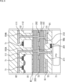
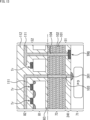
- FIG. 4 is a cross-sectional view schematically showing a first structural example of a pixel in the first embodiment;
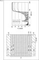
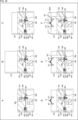
- FIG. It is a figure explaining the simulation result of a dielectric multilayer film.
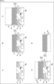
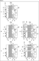
- 5A and 5B are diagrams for explaining a method of manufacturing a pixel of the first structural example of FIG. 4;
- 5A and 5B are diagrams for explaining a method of manufacturing a pixel of the first structural example of FIG. 4;
- FIG. 4 is a cross-sectional view schematically showing a second structural example of a pixel in the first embodiment
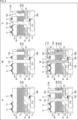
- 8A and 8B are diagrams for explaining a method of manufacturing a pixel of the second structural example of FIG. 7
- FIG. 7 is a cross-sectional view schematically showing a third structural example of the pixel in the first embodiment
- 10A and 10B are diagrams for explaining a method of manufacturing a pixel of the third structural example of FIG. 9
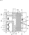
- FIG. 10 is a cross-sectional view schematically showing a fourth structural example of the pixel in the first embodiment
- FIG. 12 is a cross-sectional view schematically showing a fifth structural example of the pixel in the first embodiment
- FIG. 11 is a cross-sectional view schematically showing a sixth structural example of a pixel in the first embodiment;
- FIG. 11 is a cross-sectional view schematically showing a seventh structural example of a pixel in the first embodiment;
- FIG. 11 is a cross-sectional view schematically showing an eighth structural example of a pixel in the first embodiment;
- FIG. 20 is a cross-sectional view schematically showing a ninth structural example of the pixel in the first embodiment;
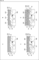
- 16A and 16B are diagrams illustrating a method of manufacturing a pixel in the eighth structural example of FIG. 15 and the ninth structural example of FIG. 16;
- FIG. 10 is a diagram schematically showing a first structural example of a pixel in the second embodiment;
- FIG. 11 is a cross-sectional view schematically showing a fifth structural example of a pixel in the second embodiment
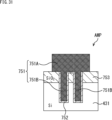
- FIG. 14 is an enlarged cross-sectional view of the vicinity of the gate electrode of the amplification transistor in the fifth structural example
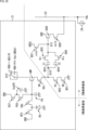
- FIG. 5 is a diagram showing another circuit configuration example of a pixel
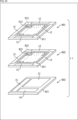
- It is a figure which shows the schematic structural example of the solid-state imaging device at the time of laminating
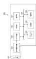
- 1 is a block diagram showing a configuration example of an imaging device as an electronic device to which technology of the present disclosure is applied
- FIG. 1 is a block diagram showing an example of a schematic configuration of a vehicle control system
- FIG. FIG. 4 is an explanatory diagram showing an example of installation positions of an outside information detection unit and an imaging unit;
- the definitions of directions such as up and down in the following description are merely definitions for convenience of description, and do not limit the technical idea of the present disclosure. For example, if an object is observed after being rotated by 90°, the upper and lower sides are converted to the left and right when read, and if the object is observed after being rotated by 180°, the upper and lower sides are reversed and read.
- FIG. 1 is a diagram showing a schematic configuration of a solid-state imaging device to which the technique of the present disclosure is applied.
- the solid-state imaging device 1 in FIG. 1 shows the configuration of a CMOS image sensor, which is a kind of X-Y addressing solid-state imaging device, for example.
- a CMOS image sensor is an image sensor manufactured by applying or partially using a CMOS process.
- the solid-state imaging device 1 includes a pixel array section 11 and a peripheral circuit section.
- the peripheral circuit section includes, for example, a vertical driving section 12, a column processing section 13, a horizontal driving section 14, and a system control section 15. FIG.
- the solid-state imaging device 1 further includes a signal processing section 16 and a data storage section 17 .
- the signal processing unit 16 and the data storage unit 17 may be mounted on the same substrate as the pixel array unit 11, the vertical driving unit 12, etc., or may be arranged on a separate substrate. Further, each process of the signal processing unit 16 and the data storage unit 17 may be executed by an external signal processing unit provided on a semiconductor chip different from the solid-state imaging device 1, such as a DSP (Digital Signal Processor) circuit. good.
- DSP Digital Signal Processor
- the pixel array section 11 has a configuration in which a plurality of pixels 21 are two-dimensionally arranged in rows and columns.
- the row direction refers to the pixel rows of the pixel array section 11, that is, the horizontal arrangement direction
- the column direction refers to the pixel columns of the pixel array section 11, that is, the vertical arrangement direction.
- the pixel 21 has a photoelectric conversion unit that generates and accumulates electric charges according to the amount of received light, and a plurality of pixel transistors (so-called MOS transistors). A specific circuit configuration example of the pixel 21 will be described later with reference to FIG.
- pixel drive wirings 22 as row signal lines are wired along the row direction for each pixel row, and vertical signal lines 23 as column signal lines are wired along the column direction for each pixel column. It is The pixel drive wiring 22 transmits drive signals for driving when reading out signals from the pixels 21 .
- the pixel driving wiring 22 is shown as one wiring, but the number is not limited to one.
- One end of the pixel driving wiring 22 is connected to an output terminal corresponding to each row of the vertical driving section 12 .
- the vertical driving section 12 is composed of a shift register, an address decoder, etc., and drives each pixel of the pixel array section 11 simultaneously or in units of rows.
- the vertical driving section 12 constitutes a driving section that controls the operation of each pixel of the pixel array section 11 together with the system control section 15 .
- the vertical drive unit 12 generally has two scanning systems, a readout scanning system and a sweeping scanning system, although the specific configuration is not shown.
- the readout scanning system sequentially selectively scans the pixels 21 of the pixel array section 11 row by row in order to read out signals from the pixels 21 .
- a signal read out from the pixel 21 is an analog signal.
- the sweep-scanning system performs sweep-scanning ahead of the read-out scanning by the exposure time for the read-out rows to be read-scanned by the read-out scanning system.
- a so-called electronic shutter operation is performed by sweeping out (resetting) unnecessary charges by this sweeping scanning system.
- the electronic shutter operation refers to an operation of discarding the charge in the photoelectric conversion unit and starting new exposure (starting charge accumulation).
- the signal read out by the readout operation by the readout scanning system corresponds to the amount of light received after the immediately preceding readout operation or the electronic shutter operation.
- a period from the readout timing of the previous readout operation or the sweep timing of the electronic shutter operation to the readout timing of the current readout operation is the exposure period of the pixel 21 .
- a signal output from each pixel 21 in a pixel row selectively scanned by the vertical driving unit 12 is input to the column processing unit 13 through each vertical signal line 23 for each pixel column.
- the column processing unit 13 performs predetermined signal processing on signals output from the pixels 21 of the selected row through the vertical signal lines 23 for each pixel column of the pixel array unit 11, and converts the pixel signals after the signal processing. hold temporarily.
- the column processing unit 13 performs at least noise removal processing, such as CDS (Correlated Double Sampling) processing and DDS (Double Data Sampling) processing, as signal processing.
- CDS Correlated Double Sampling
- DDS Double Data Sampling
- the CDS processing removes pixel-specific fixed pattern noise such as reset noise and variations in threshold values of amplification transistors in pixels.
- the column processing unit 13 may be provided with, for example, an AD (analog-digital) conversion function to convert an analog pixel signal into a digital signal and output the digital signal.
- AD analog-digital
- the horizontal driving section 14 is composed of a shift register, an address decoder, etc., and selects unit circuits corresponding to the pixel columns of the column processing section 13 in order. By selective scanning by the horizontal driving section 14, pixel signals that have undergone signal processing for each unit circuit in the column processing section 13 are sequentially output.
- the system control unit 15 includes a timing generator that generates various timing signals, and controls the vertical driving unit 12, the column processing unit 13, the horizontal driving unit 14, etc. based on the various timings generated by the timing generator. drive control.
- the signal processing unit 16 has at least an arithmetic processing function, and performs various signal processing such as arithmetic processing on pixel signals output from the column processing unit 13 .
- the data storage unit 17 temporarily stores data required for signal processing in the signal processing unit 16 .
- the pixel signals that have undergone signal processing in the signal processing section 16 are converted into a predetermined format and output from the output section 18 to the outside of the apparatus.
- FIG. 2 is a diagram showing a circuit configuration example of one pixel 21 provided in the pixel array section 11. As shown in FIG.
- one pixel 21 is configured to include a photodiode PD, a transfer transistor TRG, a floating diffusion region FD, a reset transistor RST, an amplification transistor AMP, and a selection transistor SEL.
- the transfer transistor TRG, reset transistor RST, amplification transistor AMP, and selection transistor SEL are composed of, for example, N-type MOS transistors (MOS FETs).
- the photodiode PD is a photoelectric conversion unit provided in the pixel 21, receives light from the subject, generates and accumulates charges according to the amount of light received by photoelectric conversion.
- the photodiode PD has an anode terminal grounded and a cathode terminal connected to the floating diffusion region FD via the transfer transistor TRG.
- the transfer transistor TRG is provided between the photodiode PD and the floating diffusion region FD. transfer to
- the floating diffusion region FD is a voltage converter that converts the charge transferred from the photodiode PD via the transfer transistor TRG into an electric signal, for example, a voltage signal and outputs the signal.
- the floating diffusion region FD is also connected to the source of the reset transistor RST and the gate of the amplification transistor AMP.
- the reset transistor RST When the reset transistor RST is turned on by a reset drive signal supplied to its gate, the charges accumulated in the floating diffusion region FD are discharged to the drain (constant voltage source VDD), resetting the potential of the floating diffusion region FD. .
- the amplification transistor AMP outputs a pixel signal according to the potential of the floating diffusion region FD. That is, the amplification transistor AMP forms a source follower circuit together with the constant current source 24 connected via the vertical signal line 23, and the pixel signal VSL indicating the level corresponding to the charge accumulated in the floating diffusion region FD is , is output from the amplification transistor AMP to the column processing unit 13 (FIG. 1) via the selection transistor SEL.
- the constant current source 24 is provided in the column processing section 13, for example.
- the selection transistor SEL is connected between the source of the amplification transistor AMP and the vertical signal line 23, and a selection drive signal is supplied to the gate of the selection transistor SEL.
- the selection transistor SEL When the selection transistor SEL is turned on by the selection drive signal, the selection transistor SEL becomes conductive, and the pixel 21 provided with the selection transistor SEL is selected.
- the pixel signal VSL output from the amplification transistor AMP is read out to the column processing section 13 via the vertical signal line 23 .
- a transfer drive signal, a reset drive signal, and a selection drive signal supplied to the gates of the transfer transistor TRG, reset transistor RST, and selection transistor SEL are vertically driven by a row signal line corresponding to the pixel drive wiring 22 in FIG. It is transmitted from the unit 12 .
- the transfer drive signal, the reset drive signal, and the selection drive signal are pulse signals whose high level state is an active state (on state) and whose low level state is an inactive state (off state).
- the pixel 21 has the circuit configuration as described above.
- each pixel 21 may have a shared pixel structure in which a plurality of pixels share a readout circuit.
- a shared pixel structure for example, four pixels of 2 ⁇ 2, two pixels each in the row direction and the column direction, share the floating diffusion region FD, reset transistor RST, amplification transistor AMP, and selection transistor SEL.
- a configuration in which the photodiode PD and the transfer transistor TRG are arranged for each pixel can be adopted. Note that the number of pixels in a shared unit is not limited to four pixels.
- FIG. 3 is a cross-sectional view schematically showing a first structural example of the pixel 21 according to the first embodiment.
- the pixel 21 of the first structural example is configured by stacking two substrates, a first-level pixel substrate 51 and a second-level pixel substrate 52 .
- a dashed line in FIG. 3 indicates the joint surface between the first-level pixel substrate 51 and the second-level pixel substrate 52 .
- the first-floor pixel substrate 51 is configured by laminating a semiconductor substrate 71, a wiring layer 72, and a dielectric multilayer film 73.
- the second-floor pixel substrate 52 is configured by laminating a semiconductor substrate 81, a wiring layer 82 formed on one surface of the semiconductor substrate 81, and an insulating film 83 formed on the other surface of the semiconductor substrate 81.
- the upper surface of the semiconductor substrate 71 on which the wiring layer 72 is formed is the front surface of the semiconductor substrate 71, and the surface opposite to the surface on which the wiring layer 72 is formed is It is the back surface of the semiconductor substrate 71 and is the light incident surface on which light is incident.
- a color filter layer, an on-chip lens, and the like can be formed on the back surface of the semiconductor substrate 71 as necessary.
- the upper surface of the semiconductor substrate 81 on which the wiring layer 82 is formed is the front surface of the semiconductor substrate 81
- the surface on which the insulating film 83 is formed is the back surface of the semiconductor substrate 81. is. Therefore, the first-level pixel substrate 51 and the second-level pixel substrate 52 are bonded face-to-back in which the front surface side of the semiconductor substrate 71 and the back surface side of the semiconductor substrate 81 are bonded together.
- the semiconductor substrate 71 is a substrate using, for example, silicon (Si) as a semiconductor material.
- a photodiode PD is formed on the semiconductor substrate 71 for each pixel, and a transfer transistor TRG is formed at the interface with the wiring layer 72 .
- At least the transfer transistor TRG is provided on the first-floor pixel substrate 51, but other pixel transistors may also be formed. In FIG. 3, only the gate electrode is illustrated for the transfer transistor TRG.
- the photodiode PD is configured, for example, by forming an N-type semiconductor region, which is of a conductivity type different from the P-type, in the P-type semiconductor region (P-well layer) forming the semiconductor substrate 71 . Further, in the semiconductor substrate 71, for example, a pixel isolation portion for electrically isolating a semiconductor region including the photodiode PD in the pixel from the adjacent pixel is formed at the boundary portion with the adjacent pixel. is omitted.
- the wiring layer 72 is composed of one or more layers of wiring 91 and an interlayer insulating film 92 .
- the wiring 91 is made of, for example, metals such as copper (Cu), tungsten (W), aluminum (Al), and gold (Au), or conductive polysilicon heavily doped with boron (B), phosphorus (P), or the like. made of materials such as
- the interlayer insulating film 92 is made of, for example, silicon oxide (SiO2). In the example of FIG. 3, the wiring 91 is formed in two layers in the wiring layer 72, but the wiring 91 may be formed in one layer or in three or more layers.
- the dielectric multilayer film 73 includes a first film 101 using a dielectric material having a first refractive index n1 and a second refractive index n2 ( n1 > n 2 ) using a dielectric material are alternately laminated.
- first film 101 with a higher refractive index will be referred to as a high refractive index film 101
- the second film 102 with a lower refractive index will be referred to as a low refractive index film 102 in the following description.
- the number of laminated layers of the high refractive index films 101 and the low refractive index films 102 laminated alternately is 12, but the dielectric multilayer film 73 may be formed by laminating at least three layers. Just do it.
- the dielectric multilayer film 73 is formed over the entire light-receiving region of the pixel array section 11 in the planar direction. However, the dielectric multilayer film 73 is open in the regions where the through electrodes 103 and 104 electrically connecting the first-story pixel substrate 51 and the second-story pixel substrate 52 are arranged.
- the dielectric material of the high refractive index film 101 and the low refractive index film 102 can be formed on the substrate by, for example, the CVD (Chemical Vapor Deposition) method, the sputtering method, the plating method, etc. Any material can be used as long as it can be controlled. In addition, it is desirable to use an insulating material in order to suppress short-circuit defects with the through electrodes 103 and 104 .
- CVD Chemical Vapor Deposition
- dielectric materials for the high refractive index film 101 and the low refractive index film 102 include silicon compounds such as SiOx, SiN, and SiC, polysilicon (polySi), amorphous silicon (a-Si), TiO2, Al2O3, Metal compounds including oxides or nitrides such as TiN can be used. These dielectric materials have high melting points and heat resistance.
- the dielectric multilayer film 73 is configured by alternately stacking two types of films having different refractive indices, but may be configured by stacking three or more types of films.
- the semiconductor substrate 81 is a substrate made up of, for example, a P-type semiconductor region using, for example, silicon (Si) as a semiconductor material.
- a plurality of pixel transistors Tr are formed on the wiring layer 82 side surface, which is the front surface of the semiconductor substrate 81 .
- These plurality of pixel transistors Tr are pixel transistors that are not provided on the first-floor pixel substrate 51 .
- the pixel transistor formed on the first-level pixel substrate 51 is only the transfer transistor TRG, the reset transistor RST, the amplification transistor AMP, and the selection transistor SEL are each formed on the second-level pixel substrate 52 as the pixel transistor Tr. be.
- the reset transistor RST and the selection transistor SEL are formed on the second floor pixel substrate 52 as the pixel transistors Tr.
- the through electrode 103 penetrates the semiconductor substrate 81 and the dielectric multilayer film 73, and connects predetermined wiring 111 of the second-level pixel substrate 52 and predetermined diffusion layers (not shown) of the semiconductor substrate 71 of the first-level pixel substrate 51. Connected.
- the through electrode 103 and the dielectric multilayer film 73 are separated by an insulating film 105 .
- the through-electrode 104 penetrates the semiconductor substrate 81 and the dielectric multilayer film 73 and connects the prescribed wiring 111 of the second-story pixel substrate 52 and the prescribed wiring 91 of the first-story pixel substrate 51 .
- the through electrode 104 and the dielectric multilayer film 73 are separated by an insulating film 106 .
- the wiring layer 82 is composed of one or more layers of wiring 111 and an interlayer insulating film 112 .
- the number of layers of the wiring 111 is one for the sake of simplification.
- the wiring 111 is formed of materials such as copper (Cu), tungsten (W), aluminum (Al), and gold (Au), for example.
- the interlayer insulating film 112 is made of, for example, silicon oxide (SiO2).
- the insulating film 83 formed on the back side of the semiconductor substrate 81 (lower side in FIG. 3) is made of, for example, silicon oxide (SiO2).
- the solid-state imaging device 1 is configured by stacking the first-level pixel substrate 51 and the second-level pixel substrate 52 . At least a photodiode PD and a transfer transistor TRG provided for each pixel are formed on the first-floor pixel substrate 51 . Other pixel transistors Tr that are not formed on the first-level pixel substrate 51 are formed on the second-level pixel substrate 52 . When only one pixel transistor Tr is formed on the first-level pixel substrate 51, the pixel transistor Tr is the transfer transistor TRG, and the reset transistor RST, amplification transistor AMP, and selection transistor SEL are formed on the second-level pixel substrate. 52.
- the high refractive index film 101 and the low refractive index film are interposed between the semiconductor substrate 71 of the first floor pixel substrate 51 and the semiconductor substrate 81 of the second floor pixel substrate 52.
- a dielectric multilayer film 73 formed by laminating at least three layers of 102 is arranged.
- the dielectric multilayer film 73 reflects light that is incident from the rear surface (lower surface in FIG. 3) of the semiconductor substrate 71 , which is the light incident surface, and passes through the wiring layer 72 to reach the second-level pixel substrate 52 .
- FIG. 4 shows the result of simply estimating the light reflectance of the dielectric multilayer film 73 using the effective Fresnel coefficient method.
- the inventor used titanium oxide (TiO2) as the high refractive index film 101 and silicon oxide (SiO2) as the low refractive index film 102, and formed an N layer (
- the dielectric multilayer film 73 was configured with N>2), and the reflectance was calculated for each wavelength when light was vertically incident. It is assumed that the refractive index n is independent of wavelength.
- the film thickness of the high refractive index film 101 is 70 nm, and the refractive index n1 of titanium oxide (TiO2) is approximately 2.7.
- the film thickness of the low refractive index film 102 is 140 nm, and the refractive index n2 of silicon oxide (SiO2) is approximately 1.5.
- the films above and below the dielectric multilayer film 73 are made of silicon oxide (SiO2), which is the same as the low refractive index film 102 .
- the graph on the right side of FIG. 4 shows the simulation results of calculating the reflectance for each wavelength.
- a high reflectance is obtained for light with long wavelengths, specifically light with a wavelength of 730 nm or more, which is not easily absorbed by silicon and is easily transmitted to the second-floor pixel substrate 52 .
- the combination of dielectric materials and film thicknesses of the high refractive index film 101 and the low refractive index film 102 is not limited to this.
- the dielectric multilayer film 73 blocks light that is incident from the back surface (bottom surface in FIG. 3) of the semiconductor substrate 71, which is the light incident surface, and passes through the wiring layer 72 to reach the second-level pixel substrate 52. can be reflected.
- the transmittance of light to the second-story pixel substrate 52 can be reduced, so that the parasitic photosensitivity (PLS) in the second-story pixel substrate 52 can be suppressed.
- the dielectric material forming the dielectric multilayer film 73 has heat resistance, a shield layer having both a shielding effect and heat resistance can be formed.
- a photodiode PD is formed by forming an N-type semiconductor region on a semiconductor substrate 71 formed of a P-type semiconductor region, and then a transfer transistor TRG is formed. is formed. Then, the wiring layer 72 is formed by alternately laminating the wiring 91 and the interlayer insulating film 92 using the dual damascene method or the like on the surface on which the transfer transistor TRG is formed.
- a dielectric multilayer film 73 is formed by alternately laminating high refractive index films 101 and low refractive index films 102 on the upper surface of the wiring layer 72 .
- the number of laminated layers of the high refractive index film 101 and the low refractive index film 102 is three or more.
- a method for forming the high refractive index film 101 and the low refractive index film 102 for example, a method such as a CVD method, a sputtering method, or a plating method can be used to form a film on a substrate and the film thickness can be accurately controlled during film formation. Adopted.
- An insulating film for bonding to the semiconductor substrate 81 of the second-level pixel substrate 52 may be further formed on the upper surface of the dielectric multilayer film 73 .
- the first floor pixel substrate 51 is completed by the state shown in FIG. 5B.
- a semiconductor substrate 81 having an insulating film 83 formed on one surface of the substrate is prepared.
- the semiconductor substrate 81 and the dielectric multilayer film 73 of the first-floor pixel substrate 51 are bonded by, for example, plasma bonding, the semiconductor substrate 81 is thinned as shown in FIG. become. Note that when an SOI (Silicon on Insulator) substrate is used as the semiconductor substrate 81, the thinning step is omitted.
- SOI Silicon on Insulator
- the dielectric multilayer film 73 was formed on the wiring layer 72 of the semiconductor substrate 71 on the first-level pixel substrate 51 side.
- a dielectric multilayer film 73 may be formed on the insulating film 83 of the substrate 81 and bonded to the first floor pixel substrate 51 .
- the bonding surface between the first-level pixel substrate 51 and the second-level pixel substrate 52 is the surface where the dielectric multilayer film 73 and the wiring layer 72 are in contact with each other, as shown in D of FIG.
- a plurality of pixel transistors Tr are formed on the top surface (front surface) of the semiconductor substrate 81 bonded to the first-floor pixel substrate 51 .
- These pixel transistors Tr correspond to, for example, a reset transistor RST, an amplification transistor AMP, or a selection transistor SEL.
- through holes 151 and 152 that penetrate at least the semiconductor substrate 81 and the dielectric multilayer film 73 are formed.
- Through-holes 151 and 152 correspond to regions where through-electrodes 103 and 104 are to be formed, respectively, and are formed by etching semiconductor substrate 81, dielectric multilayer film 73, wiring layer 72, and the like.
- the through-hole 151 is formed to a depth reaching the semiconductor substrate 71 of the first-level pixel substrate 51
- the through-hole 152 is formed to a depth reaching the wiring 91 of the wiring layer 72 of the first-level pixel substrate 51 .
- an insulating film 112A is formed inside the formed through-holes 151 and 152 and above the surface of the semiconductor substrate 81 on which the pixel transistor Tr is formed, and then planarized. be.
- through holes 161 and 162 are formed in regions corresponding to the through electrodes 103 and 104 by performing dry etching or the like from the upper surface of the insulating film 112A.
- the portions of the insulating film 112A remaining around the through holes 161 and 162 correspond to the insulating films 105 and 106, respectively.
- a metal material such as tungsten (W), which will become the through electrodes 103 and 104 is deposited inside the formed through holes 161 and 162 using the dual damascene method or the like.
- tungsten (W) which will become the through electrodes 103 and 104 is deposited inside the formed through holes 161 and 162 using the dual damascene method or the like.
- copper (Cu), etc., and interconnects 111 connected to the through holes 161 and 162 are formed on the upper surface of the insulating film 112A.
- an insulating film is formed on the upper surface of the wiring 111, and a wiring layer 82 composed of the wiring 111 and the interlayer insulating film 112 is formed to complete the second-level pixel substrate 52, and the pixel structure shown in FIG. is completed.
- the dielectric multilayer film 73 since the dielectric material forming the dielectric multilayer film 73 has heat resistance, the dielectric multilayer film 73 is After formation, active elements such as pixel transistors Tr can be formed on the second-level pixel substrate 52 . As a result, the flexibility of the process can be improved, and the solid-state imaging device 1 can be efficiently manufactured in a short period of time.
- FIG. 7 is a cross-sectional view schematically showing a second structural example of the pixel 21 in the first embodiment.
- insulating films 105 and 106 were formed around the peripheries of the through electrodes 103 and 104, respectively.
- the insulating film 105 is not formed around the through electrode 103, and the through electrode 103 and the dielectric multilayer film 73 are in contact with each other.
- the through electrode 104 does not have the insulating film 106 formed around the perimeter of the through electrode 104, and the through electrode 104 and the dielectric multilayer film 73 are in contact with each other.
- the insulating films 105 and 106 inserted between the through electrode 103 or 104 and the dielectric multilayer film 73 are omitted, light can be further prevented from entering, the effect of suppressing parasitic light sensitivity in the second-story pixel substrate 52 can be further enhanced.
- the state shown in A of FIG. 8 is the same as the state of A of FIG. 6 described in the manufacturing method of the pixel 21 of the first structural example. be done.
- the semiconductor substrate 81 and the first floor pixel substrate 51 are bonded together, and a plurality of pixel transistors Tr are formed on the upper surface of the semiconductor substrate 81. state.
- through holes 171 and 172 are formed through the semiconductor substrate 81 .
- the through-holes 171 and 172 correspond to regions where the through-electrodes 103 and 104 are formed, respectively, and are formed to a depth reaching the dielectric multilayer film 73 of the first-level pixel substrate 51 .
- an insulating film 112A is formed inside the formed through holes 171 and 172 and above the surface of the semiconductor substrate 81 on which the pixel transistor Tr is formed, and then planarized. be.
- through holes 181 and 182 are formed in regions corresponding to the through electrodes 103 and 104 by performing dry etching or the like from the upper surface of the insulating film 112A.
- a metal material for example, tungsten (W), which will become the through electrodes 103 and 104, is deposited inside the formed through holes 181 and 182 using the dual damascene method or the like.
- copper (Cu), etc., and wiring 111 connected to each of the through holes 181 and 182 is formed on the upper surface of the insulating film 112A.
- an insulating film is formed on the upper surface of the wiring 111, and a wiring layer 82 composed of the wiring 111 and the interlayer insulating film 112 is formed, thereby completing the second floor pixel substrate 52 and the pixel structure shown in FIG. is completed.
- active elements such as the pixel transistor Tr can be formed on the second floor pixel substrate 52 after the dielectric multilayer film 73 is formed. .
- the flexibility of the process can be improved, and the solid-state imaging device 1 can be efficiently manufactured in a short period of time.
- FIG. 9 is a cross-sectional view schematically showing a third structural example of the pixel 21 in the first embodiment.
- the third structural example shown in FIG. 9 differs from the first structural example shown in FIG.
- the through electrode 103 in the first structural example of FIG. 3 is changed to a through electrode 103A.
- the through electrode 103A penetrates the semiconductor substrate 81 and is connected to the wiring 201 .
- the through electrode 104 in the first structural example of FIG. 3 is changed to a through electrode 104A.
- the through electrode 104A penetrates the semiconductor substrate 81 and is connected to the wiring 202 .
- the insulating film 105 is not formed around the perimeter of the through electrode 103A, and the through electrode 103A and the dielectric multilayer film 73 are in contact with each other.
- the through electrode 104A does not have the insulating film 106 formed around the perimeter of the through electrode 104A, and the through electrode 104A and the dielectric multilayer film 73 are in contact with each other.
- the wiring 201 is also connected to a predetermined diffusion layer (not shown) of the semiconductor substrate 71 by a contact wiring 211 .
- the wiring 202 is also connected to a predetermined wiring 91 in the wiring layer 72 by a contact wiring 212 .
- the dielectric multilayer film 73 is interposed between the semiconductor substrate 81 of the second-level pixel substrate 52 and the semiconductor substrate 71 of the first-level pixel substrate 51.
- the wirings 201 to 203 are provided in the dielectric multilayer film 73, the aspect ratio of the through electrodes 103A and 104A is reduced, so the difficulty of forming the through electrodes can be reduced. Furthermore, since the diameters of the through electrodes 103A and 104A can be reduced, the area efficiency can be improved, and the total thickness of the solid-state imaging device 1 can be reduced.
- a dielectric multilayer film 73 corresponding to a part of the finally formed dielectric multilayer film 73 is formed on the wiring layer 72 of the semiconductor substrate 71 on which the photodiode PD and the transfer transistor TRG are formed.
- a body multilayer film 73X is formed.
- the dielectric multilayer film 73X is formed of 7 layers, whereas the final dielectric multilayer film 73 is formed of 12 layers.
- the regions of the dielectric multilayer film 73X where the wirings 201 to 203 are to be formed are etched to form trenches 231 to 233. Then, as shown in FIG. 10B, the regions of the dielectric multilayer film 73X where the wirings 201 to 203 are to be formed are etched to form trenches 231 to 233. Then, as shown in FIG. 10B, the regions of the dielectric multilayer film 73X where the wirings 201 to 203 are to be formed are etched to form trenches 231 to 233. Then, as shown in FIG.
- contact wires 211 and 212 and wires 201 to 203 are formed using a dual damascene method or the like.
- the remaining high refractive index films 101 and low refractive index films 102 are alternately formed on the upper surface of the layer in which the wirings 201 to 203 are formed. is completed.
- the process after forming the first-floor pixel substrate 51 is the same as the manufacturing method of the first structural example described above. Specifically, the same steps as those from the step of C in FIG. 5 to the step of E in FIG. 6 are performed.
- active elements such as the pixel transistor Tr can be formed on the second-level pixel substrate 52 after the dielectric multilayer film 73 is formed.
- the flexibility of the process can be improved, and the manufacturing can be efficiently performed in a short period of time.
- FIG. 11 is a cross-sectional view schematically showing a fourth structural example of the pixel 21 in the first embodiment.
- the wiring layer 72 is arranged between the semiconductor substrate 71 and the dielectric multilayer film 73 .
- a wiring layer 72 is formed on the .
- the dielectric multilayer film 73 is arranged between the semiconductor substrate 71 and the wiring layer 72 .
- An insulating film 241 is inserted between the dielectric multilayer film 73 and the semiconductor substrate 71 .
- the through electrodes 103 and 104 in the first structural example of FIG. 3 are changed to through electrodes 103A and 104A in FIG.
- the through electrode 103A penetrates through the semiconductor substrate 81 of the second-story pixel substrate 52 and is connected to the predetermined wiring 91 of the wiring layer 72 in common, but in the fourth structural example, the wiring layer 72 is a dielectric multilayer film.
- the aspect ratios of the through electrodes 103A and 104A are smaller than those of the through electrodes 103 and 104 of the first structural example because they are arranged on the second floor pixel substrate 52 side of the through electrodes 73 .
- penetrating electrodes 251 and 252 that penetrate the dielectric multilayer film 73 of the first-floor pixel substrate 51 are provided.
- the through electrodes 251 and 252 connect the wiring 91 different from the wiring 91 to which the through electrodes 103A and 104A are connected, and the semiconductor substrate 71 of the first-floor pixel substrate 51, respectively.
- the dielectric multilayer film 73 is provided between the semiconductor substrate 81 of the second-level pixel substrate 52 and the semiconductor substrate 71 of the first-level pixel substrate 51.
- the aspect ratio of the through electrodes 103A and 104A is reduced, the diameter can be reduced, so that the area efficiency can be improved. Moreover, the degree of difficulty in forming the through electrodes can be reduced.
- the dielectric multilayer film 73 is arranged at a position closer to the semiconductor substrate 71 of the first-floor pixel substrate 51, the reflection by the dielectric multilayer film 73 is closer to the semiconductor substrate 71 as indicated by the arrow in FIG. Since it occurs at a position, it is possible to prevent light from leaking into adjacent pixels and prevent color mixture.
- FIG. 12 is a cross-sectional view schematically showing a fifth structural example of the pixel 21 in the first embodiment.
- the arrangement of the wiring layer 72 and the dielectric multilayer film 73 of the first-floor pixel substrate 51 is changed compared to the first structural example shown in FIG. , was formed between the semiconductor substrate 71 and the wiring layer 72 .
- the first wiring layer 72A and the second wiring layer 72B are formed on the first-level pixel substrate 51, and the dielectric multilayer film 73 is the first wiring layer. It is formed between the wiring layer 72A and the second wiring layer 72B.
- the first wiring layer 72A includes one or more wiring layers 91A and an interlayer insulating film 92A, and is arranged between the semiconductor substrate 71 and the dielectric multilayer film 73.
- the second wiring layer 72B includes one or more layers of wiring 91B and an interlayer insulating film 92B, and is formed between the dielectric multilayer film 73 and the semiconductor substrate 81 of the second-level pixel substrate 52.
- the through-electrode 103A connects the prescribed wiring 111 of the second-story pixel substrate 52 and the prescribed wiring 91B of the second wiring layer 72B of the first-story pixel substrate 51 .
- the through electrode 104A connects the prescribed wiring 111 of the second-story pixel substrate 52 and the prescribed wiring 91B of the second wiring layer 72B of the first-story pixel substrate 51 .
- the wirings 111 and 91B connected to the through electrode 104A are different wirings from the wirings 111 and 91B connected to the through electrode 103A.
- a through-electrode 271 penetrating through the dielectric multilayer film 73 is provided on the first-floor pixel substrate 51 .
- the through electrode 271 connects a predetermined wiring 91A of the first wiring layer 72A and a predetermined wiring 91B of the second wiring layer 72B.
- the transfer transistor TRG not only the transfer transistor TRG but also the amplification transistor AMP are formed on the first-floor pixel substrate 51 side as pixel transistors.
- FIG. 12 illustration of the transfer transistor TRG is omitted, and the amplification transistor AMP is illustrated.
- a gate electrode of the amplification transistor AMP is connected to a floating diffusion region FD (not shown) formed in the semiconductor substrate 71 by a predetermined wiring 281 formed in the first wiring layer 72A.
- the dielectric multilayer film 73 is interposed between the semiconductor substrate 81 of the second-level pixel substrate 52 and the semiconductor substrate 71 of the first-level pixel substrate 51. By arranging them, the effect of suppressing the parasitic light receiving sensitivity and the effect of electromagnetic shielding can be achieved.
- the aspect ratio of the through electrodes 103A and 104A is reduced, the diameter can be reduced, so that the area efficiency can be improved. Moreover, the degree of difficulty in forming the through electrodes can be reduced.
- the wiring 281 between the floating diffusion region FD formed in the semiconductor substrate 71 and the gate electrode of the amplification transistor AMP is eliminated. Since the wiring length can be shortened, the photoelectric conversion efficiency can be increased.
- FIG. 13 is a cross-sectional view schematically showing a sixth structural example of the pixel 21 in the first embodiment.
- the through-electrode 103 penetrates the semiconductor substrate 81 and the dielectric multilayer film 73 and connects the predetermined wiring 111 of the second-story pixel substrate 52 and the diffusion layer 301 of the semiconductor substrate 71 of the first-story pixel substrate 51 .
- No insulating film 105 is formed between the through electrode 103 and the dielectric multilayer film 73, and the through electrode 103 and the dielectric multilayer film 73 are in contact with each other.
- the through electrode 104 penetrates the semiconductor substrate 81 and the dielectric multilayer film 73, and connects the predetermined wiring 111 of the second floor pixel substrate 52 and the gate electrode of the transfer transistor TRG of the first floor pixel substrate 51.
- the insulating film 106 is not formed between the through electrode 104 and the dielectric multilayer film 73, and the through electrode 104 and the dielectric multilayer film 73 are in contact with each other.
- the dielectric multilayer film 73 is interposed between the semiconductor substrate 81 of the second-level pixel substrate 52 and the semiconductor substrate 71 of the first-level pixel substrate 51.
- a dielectric multilayer film 73 and an insulating film 241 are provided between the semiconductor substrate 81 of the second-level pixel substrate 52 and the semiconductor substrate 71 of the first-level pixel substrate 51, and the wiring layer 72 is omitted.
- the overall thickness of the imaging device 1 can be reduced.
- FIG. 14 is a cross-sectional view schematically showing a seventh structural example of the pixel 21 according to the first embodiment.
- an insulating film 241 is formed on a semiconductor substrate 71 of a first-floor pixel substrate 51, and a first dielectric multilayer film 73A and a first wiring layer 72A are formed on the insulating film 241.
- a second dielectric multilayer film 73B and a second wiring layer 72B are formed on the first wiring layer 72A.
- the second wiring layer 72B of the 1st floor pixel substrate 51 and the insulating film 83 on the back surface of the semiconductor substrate 81 of the 2nd floor pixel substrate 52 are joined.
- the dielectric multilayer film 73 formed of one layer in the first structural example and the like described above is replaced by the first dielectric multilayer film 73A and the second dielectric multilayer film in the seventh structural example of FIG. It has been changed to two layers of 73B.
- the wiring layer 72 which was formed of one layer in the first structural example and the like described above, is changed to two layers, a first wiring layer 72A and a second wiring layer 72B, in the seventh structural example of FIG. It is The first dielectric multilayer film 73A is arranged between the semiconductor substrate 71 and the first wiring layer 72A, and the second dielectric multilayer film 73B is arranged between the first wiring layer 72A and the second wiring layer 72B. is placed between Each of the first dielectric multilayer film 73A and the second dielectric multilayer film 73B is configured by laminating at least three layers of a high refractive index film 101 and a low refractive index film 102.
- the through-electrode 103A connects the prescribed wiring 111 of the second-story pixel substrate 52 and the prescribed wiring 91B of the second wiring layer 72B of the first-story pixel substrate 51 .
- the through electrode 104A connects the prescribed wiring 111 of the second-story pixel substrate 52 and the prescribed wiring 91B of the second wiring layer 72B of the first-story pixel substrate 51 .
- the wirings 111 and 91B connected to the through electrode 104A are different wirings from the wirings 111 and 91B connected to the through electrode 103A.
- a through-electrode 321 penetrating through the first dielectric multilayer film 73A connects a predetermined diffusion layer (not shown) of the semiconductor substrate 71 of the first-level pixel substrate 51 and a predetermined wiring 91A of the first wiring layer 72A. are doing. No insulating film is formed between the through electrode 321 and the first dielectric multilayer film 73A, and the through electrode 321 and the first dielectric multilayer film 73A are in contact with each other.
- a through electrode 322 penetrating through the first dielectric multilayer film 73A connects a prescribed diffusion layer (not shown) of the semiconductor substrate 71 of the first-level pixel substrate 51 and a prescribed wiring 91A of the first wiring layer 72A. are doing. No insulating film is formed between the through electrode 322 and the first dielectric multilayer film 73A, and the through electrode 322 and the first dielectric multilayer film 73A are in contact with each other.
- the wiring 91A to which the through electrode 321 is connected is a different wiring from the wiring 91A to which the through electrode 322 is connected.
- a through-electrode 323 passing through the second dielectric multilayer film 73B connects a predetermined wiring 91A of the first wiring layer 72A and a predetermined wiring 91B of the second wiring layer 72B.
- No insulating film is formed between the through electrode 323 and the second dielectric multilayer film 73B, and the through electrode 323 and the second dielectric multilayer film 73B are in contact with each other.
- the first dielectric multilayer is formed between the semiconductor substrate 81 of the second-level pixel substrate 52 and the semiconductor substrate 71 of the first-level pixel substrate 51.
- the first dielectric multilayer film 73A and the second dielectric multilayer film 73B are arranged by dividing the dielectric multilayer film into two layers, the first dielectric multilayer film 73A and the second dielectric multilayer film 73B. 2, the aspect ratio of the through electrodes 321 to 323 penetrating through the dielectric multilayer film 73B is reduced. As a result, since the diameters of the through electrodes 321 to 323 can be reduced, the area efficiency can be improved. Moreover, the degree of difficulty in forming the through electrodes can be reduced.
- FIG. 15 is a cross-sectional view schematically showing an eighth structural example of the pixel 21 according to the first embodiment.
- the dielectric multilayer film 73 partially blocks the light incident on each pixel 21 of the pixel array section 11 in the plane direction. It is formed only in the region to be suppressed.
- the region where light incidence is desired to be suppressed is, for example, a region corresponding to the diffusion layer formed on the semiconductor substrate 81 of the second-story pixel substrate 52 .
- the interlayer insulating film 92 of the wiring layer 72 is formed in the region where the dielectric multilayer film 73 is not formed.
- the region between the semiconductor substrate 81 of the second-story pixel substrate 52 and the semiconductor substrate 71 of the first-story pixel substrate 51 where light incidence is desired to be suppressed By arranging the dielectric multilayer film 73 in the region, the effect of suppressing the parasitic photosensitivity and the effect of electromagnetic shielding can be achieved.
- the dielectric multilayer film 73 is not arranged in the region where light incidence does not need to be suppressed, and the light is not reflected (transmitted to the semiconductor substrate 81 of the second-floor pixel substrate 52). As a result, it is possible to prevent light from leaking into adjacent pixels and prevent color mixture.
- FIG. 16 is a cross-sectional view schematically showing a ninth structural example of the pixel 21 according to the first embodiment.
- a ninth structural example in FIG. 16 corresponds to a modification of the eighth structural example shown in FIG.
- the dielectric multilayer film 73 is a part of the light receiving region of the pixel array section 11 in the plane direction, more specifically, the light incident on each pixel 21 of the pixel array section 11. was formed only for the region where it is desired to suppress .
- An interlayer insulating film 92 is formed in a region where light incidence does not need to be suppressed.
- the body multilayer film 73 has two regions with different lamination numbers in the planar direction.
- the dielectric multilayer film 73 is formed with a smaller number of layers (four layers in this example) than in the areas where the light incidence of each pixel 21 does not need to be suppressed.
- An insulating film 341 is formed in a region on the dielectric multilayer film 73 formed with a smaller number of laminations than the region where light incidence is desired to be suppressed, thereby filling a step due to a difference in the number of laminations.
- the region between the semiconductor substrate 81 of the second-floor pixel substrate 52 and the semiconductor substrate 71 of the first-floor pixel substrate 51 where light incidence is desired to be suppressed By arranging the dielectric multilayer film 73 in the region, the effect of suppressing the parasitic photosensitivity and the effect of electromagnetic shielding can be achieved.
- the dielectric multilayer film 73 is arranged with a smaller number of layers than in areas where the incidence of light is desired to be suppressed. As a result, it is possible to prevent light from leaking into adjacent pixels and prevent color mixture.
- the state shown in A of FIG. 17 is the same as the state of B of FIG. 5 described in the manufacturing method of the pixel 21 of the first structural example. be done.
- the state shown in A of FIG. 17 is a state in which the wiring layer 72 and the dielectric multilayer film 73 are formed on the semiconductor substrate 71 of the first floor pixel substrate 51 .
- the number of layers of the high refractive index film 101 and the low refractive index film 102 of the dielectric multilayer film 73 is, for example, 12 layers.
- FIG. 17B dry etching or the like is used to remove the dielectric multilayer film 73 other than the area where light incidence of each pixel 21 is desired to be suppressed.
- An interlayer insulating film 92 is further laminated on the removed region using, for example, the CVD method, as shown in FIG. 17C.
- An interlayer insulating film 92 is also formed on the upper surface of the dielectric multilayer film 73 and planarized to form the first floor pixel substrate 51 .
- the first floor pixel substrate 51 After the first floor pixel substrate 51 is formed, it can be manufactured in the same manner as the manufacturing method of the pixel 21 of the first structural example. Specifically, the steps after C in FIG. 5 described in the first structural example are executed. For example, in the step of C of FIG. 5, the interlayer insulating film 92 of the wiring layer 72 of the first floor pixel substrate 51 and the insulating film 83 of the semiconductor substrate 81 of the second floor pixel substrate 52 side are joined. After joining the semiconductor substrate 81 on the second floor pixel substrate 52 side, a plurality of pixel transistors Tr, through electrodes 103 and 104, and the like are formed to complete the pixel 21 of the eighth structural example.
- dry etching or the like is used to partially remove a portion of the dielectric multilayer film 73 other than the region where light incidence of each pixel 21 is desired to be suppressed.
- the upper eight layers are removed in areas other than the area where light incidence is desired to be suppressed.
- An insulating film 341 is formed on the removed region by plasma CVD, for example, as shown in FIG. 17E.
- An insulating film 341 is also formed on the upper surface of the dielectric multilayer film 73 formed of 12 layers and planarized to form the first floor pixel substrate 51 .
- the first floor pixel substrate 51 After the first floor pixel substrate 51 is formed, it can be manufactured in the same manner as the manufacturing method of the pixel 21 of the first structural example. Specifically, the steps after C in FIG. 5 described in the first structural example are executed. For example, the insulating film 341 on the upper surface of the dielectric multilayer film 73 of the first-story pixel substrate 51 and the insulating film 83 of the semiconductor substrate 81 on the second-story pixel substrate 52 side are bonded. After bonding, a plurality of pixel transistors Tr, through electrodes 103 and 104, and the like are formed to complete the pixel 21 of the ninth structural example.
- active elements such as the pixel transistor Tr are formed on the second floor pixel substrate 52 after the dielectric multilayer film 73 is formed. Since it can be formed, the degree of freedom in the process can be improved, and the solid-state imaging device 1 can be efficiently manufactured in a short time.
- the pixel 21 includes a first-floor pixel substrate 51 (first substrate) including a semiconductor substrate 71 on which at least a photodiode PD provided for each pixel is formed, and an active element such as a pixel transistor Tr. is laminated with a second-floor pixel substrate 52 (second substrate) including a semiconductor substrate 81 on which is formed.
- a dielectric multilayer film 73 is formed between the semiconductor substrate 81 of the second-level pixel substrate 52 and the semiconductor substrate 71 of the first-level pixel substrate 51, at least in a region of each pixel 21 where light incidence is desired to be suppressed.
- the dielectric multilayer film 73 can form a shield layer having both shielding effect and heat resistance. That is, it is possible to suppress parasitic photosensitivity in the second-story pixel substrate 52 .
- a pixel structure is adopted in which a shield layer is provided on the semiconductor substrate so that the parasitic photosensitivity of the second-level pixel substrate can be suppressed.
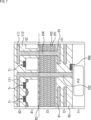
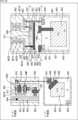
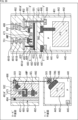
- FIG. 18 is a diagram schematically showing a first structural example of the pixel 21 according to the second embodiment.
- FIG. 18 shows a cross-sectional view of the pixel 21 of the first structural example, and the left side of FIG. ) and a plan view along the line YY' (hereinafter referred to as a YY' plan view).
- the pixel 21 of the first structural example is configured by laminating two substrates, a first-level pixel substrate 401 and a second-level pixel substrate 402 .
- a dashed line in FIG. 18 indicates the bonding surface between the first-level pixel substrate 401 and the second-level pixel substrate 402 .
- the first-floor pixel substrate 401 is configured by laminating a semiconductor substrate 421 and a wiring layer 422 .
- the second floor pixel substrate 402 is configured by laminating a semiconductor substrate 431 and a wiring layer 432 .
- the upper surface of the semiconductor substrate 421 on which the wiring layer 422 is formed in the cross-sectional view is the front surface of the semiconductor substrate 421, and the surface opposite to the surface on which the wiring layer 422 is formed.
- the surface (bottom surface in FIG. 18) is the back surface of the semiconductor substrate 421 and is the light incident surface on which light is incident.
- a color filter layer, an on-chip lens, and the like can be formed on the back surface of the semiconductor substrate 421 as necessary.
- the upper surface of the semiconductor substrate 431 on which the wiring layer 432 is formed in the cross-sectional view is the front surface of the semiconductor substrate 431, and the surface bonded to the first-level pixel substrate 51 is the surface of the semiconductor substrate 431. It is the back surface of the semiconductor substrate 431 . Therefore, the first-level pixel substrate 401 and the second-level pixel substrate 402 are bonded face-to-back in which the front surface side of the semiconductor substrate 421 and the back surface side of the semiconductor substrate 431 are bonded together.
- the semiconductor substrate 421 is a substrate using, for example, silicon (Si) as a semiconductor material.
- a semiconductor substrate 421 an N-type semiconductor region 442, which is a semiconductor region of a second conductivity type different from the P-type, is formed in a P-type semiconductor region (P well layer) 441, which is a semiconductor region of a first conductivity type.
- P well layer P-type semiconductor region
- a pixel isolation portion 443 for electrically isolating the adjacent pixels is formed in the peripheral portion of the pixel 21 in the vicinity of the boundary with the adjacent pixel of the semiconductor substrate 421.
- the pixel separating section 443 is made of, for example, an insulating film such as silicon oxide (SiO2), or a metal material such as copper (Cu), tungsten (W), or aluminum (Al).
- N-type diffusion layer 444 which is a high-concentration N-type impurity region and a P-type diffusion layer 445 which is a high-concentration P-type impurity region. is formed.
- a transfer transistor TRG is also formed.
- the transfer transistor TRG has a vertical gate electrode 446 .
- the vertical gate electrode 446 is dug to a depth reaching the N-type semiconductor region 442 formed deep in the semiconductor substrate 421 .
- the N-type diffusion layer 444 functions as part of the floating diffusion region FD, and the charge generated in the photodiode PD transferred by the transfer transistor TRG is transferred to the second-story pixel substrate 402 via the N-type diffusion layer 444. is read out to
- the P-type diffusion layer 445 is a well contact that supplies a fixed potential (eg ground or negative bias) to the P-type semiconductor region (P-well layer) 441 via the contact electrode 447 .
- a fixed potential eg ground or negative bias
- the wiring layer 422 includes not only the vertical gate electrode 446 and the contact electrode 447 of the transfer transistor TRG, but also one or more layers of wiring and the interlayer insulating film 451 .
- the interlayer insulating film 451 is formed of, for example, a silicon oxide film (SiO2). In FIG. 18, one or more layers of wiring are omitted for the sake of space.
- the semiconductor substrate 431 of the second-floor pixel substrate 402 is a substrate composed of, for example, a P-type semiconductor region using, for example, silicon (Si) as a semiconductor material.
- a reset transistor RST, an amplification transistor AMP, and a selection transistor SEL are formed on the wiring layer 432 side surface, which is the front surface of the semiconductor substrate 431.
- the periphery of each of the reset transistor RST, amplification transistor AMP, and selection transistor SEL is isolated by STI (Shallow Trench Isolation) 471 .
- a light shielding film 481 made of a metal material such as copper (Cu), tungsten (W), or aluminum (Al) is embedded at a predetermined depth in the semiconductor substrate 431 .
- the light shielding film 481 is formed on the front surface side of the semiconductor substrate 431 at a position covering a charge holding portion such as a MIM (Metal-Insulator-Metal) capacitive element and an element including a pixel transistor such as an amplifying transistor AMP. It is formed in a plane area.
- the light shielding film 481 blocks light that has passed through the semiconductor substrate 421 of the first-floor pixel substrate 401 and entered the semiconductor substrate 431 .
- Insulating films 482 are arranged above and below the light shielding film 481 .
- the insulating film 482 is composed of a single-layer or multi-layer oxide film using silicon oxide, hafnium oxide, zirconium oxide, aluminum oxide, titanium oxide, tantalum oxide, or the like, for example.
- a vertical trench 483 is formed in a region that does not interfere with elements formed on the front surface side of the semiconductor substrate 431 . are connected to the light shielding film 481 and the insulating film 482 of the .
- the light shielding film 481 in the semiconductor substrate 431 is connected to the wiring 491A through the embedded metal portion 484 embedded in the vertical trench 483 and the contact wiring 493 thereabove. Voltage is applied.
- the vertical trench 483 is formed linearly as shown in the X-X' plan view, and is filled with an insulating film 485 except for the buried metal portion 484 connected to the contact wiring 493 .
- the wiring layer 432 of the second-story pixel substrate 402 is composed of multiple layers of wiring 491 and interlayer insulating films 492 .
- the wiring layer 432 is composed of four layers of wiring 491 including wirings 491A to 491D and an interlayer insulating film 492, but the number of wiring layers 491 is not limited to four.
- a wiring 491A' formed in a predetermined region of the lowest layer in the wiring layer 432 is connected to the N-type diffusion layer 444 of the semiconductor substrate 421 of the first-floor pixel substrate 401 through the through via 501, and the contact wiring 502 is connected to the N-type diffusion layer 486 of the semiconductor substrate 431 of the second floor pixel substrate 402 via the .
- the N-type diffusion layer 444 and the N-type diffusion layer 486 electrically connected via the wiring 491A' constitute the floating diffusion region FD.
- the solid-state imaging device 1 is configured by stacking the first-level pixel substrate 401 and the second-level pixel substrate 402 . At least a photodiode PD and a transfer transistor TRG provided for each pixel are formed on the first-floor pixel substrate 401 . Other pixel transistors Tr not formed on the first-level pixel substrate 401, specifically, the reset transistor RST, the amplification transistor AMP, and the selection transistor SEL, are formed on the second-level pixel substrate 402. FIG.
- the light shielding film 481 is arranged inside the semiconductor substrate 431 of the second floor pixel substrate 402 .
- the light shielding film 481 blocks light that is incident from the rear surface (lower surface in FIG. 18) of the semiconductor substrate 421 , which is the light incident surface, and is incident on the semiconductor substrate 431 of the second-story pixel substrate 402 .
- the light-shielding film 481 is formed using a metal material, it can block noise such as surge, heat, and electromagnetism, so that the operation of the element can be stabilized.
- the semiconductor substrate of the first-layer pixel substrate and the semiconductor substrate of the second-layer pixel substrate, which are bonded together face-to-back, are covered almost entirely with a solid layer.
- the shield layer tends to have a parasitic capacitance with the wiring in the wiring layer of the first-level pixel substrate. If the wiring with the parasitic capacitance is, for example, the control wiring of the transfer transistor TRG, the parasitic capacitance reduces the read speed. Further, for example, if the wiring with the parasitic capacitance is the connection wiring of the floating diffusion region FD, the parasitic capacitance lowers the photoelectric conversion efficiency.
- the light shielding film 481 is arranged inside the semiconductor substrate 431 of the second-level pixel substrate 402, the parasitic light with the wiring layer 422 of the first-level pixel substrate 401 A free wiring design for the wiring layer 422 of the first floor pixel substrate 401 is possible without worrying about the capacitance.
- the first floor pixel substrate 401 shown in A of FIG. 19 is manufactured. Specifically, after forming the photodiode PD by forming the N-type semiconductor region 442 on the semiconductor substrate 421 formed of the P-type semiconductor region 441, the transfer transistor TRG, the N-type diffusion layer 444, and , a P-type diffusion layer 445 and the like are formed. An insulating film 551, not shown in FIG. 18, is formed on the front surface of the semiconductor substrate 421. As shown in FIG. A wiring layer 422 including one or more layers of wiring 552 and an interlayer insulating film 451 is formed on the upper surface of the insulating film 551 .
- the interlayer insulating film 451 is formed of, for example, a silicon oxide film (SiO2).
- the semiconductor substrate 431 of the second-story pixel substrate 402 is attached to the upper surface of the wiring layer 422 of the first-story pixel substrate 401 using, for example, plasma bonding. Then, as shown in FIG. 19C, the semiconductor substrate 431 is thinned to a predetermined thickness.
- pixel transistors Tr such as a reset transistor RST, an amplification transistor AMP, and a selection transistor SEL are formed on the thinned upper surface (front surface) of the semiconductor substrate 431.
- An STI 471 is formed around each pixel transistor Tr to isolate each pixel transistor Tr.
- a through hole 561 is formed by dry etching or the like at the formation position of the through via 501 that penetrates the semiconductor substrate 431 and electrically connects to the first-floor pixel substrate 401 . It is formed.
- an insulating film 492A is buried inside the through-hole 561 using, for example, the CVD method, and the insulating film 492A is also formed on the upper side of the semiconductor substrate 431 with a predetermined thickness.
- the insulating film 492A on the semiconductor substrate 431 is, for example, an SiO2 film and corresponds to part of the interlayer insulating film 492 forming the wiring layer 432.
- the insulating film 492A above the semiconductor substrate 431 is planarized by CMP (Chemical Mechanical Polishing).
- a silicon nitride film (SiN) 571 and a silicon oxide film (SiO2) 572 are laminated on the entire upper surface of the planarized insulating film 492A, and then a resist 573 is formed vertically. It is patterned so as to open the formation position of the trench 483 . Then, by performing dry etching using the patterned resist 573 as a mask, a vertical trench 574 is formed to a predetermined depth in the semiconductor substrate 431 .
- an oxide film 485A is formed on the sidewalls of the vertical trenches 574 in the semiconductor substrate 431 by thermal oxidation or the like.
- sidewalls 575 are formed on the sidewalls of the vertical trenches 574, and dry etching is performed using the sidewalls 575 as a mask, so that the bottom surface of the vertical trenches 574 has a predetermined depth. further dug up.
- the sidewalls 575 are made of, for example, a silicon nitride film (SiN).
- the side walls of the vertical trenches 574 deeper than the side walls 575 are etched in a direction parallel to the planar direction of the semiconductor substrate 431, that is, in the horizontal direction, thereby forming the horizontal trenches 581. is formed.
- This etching in the horizontal direction can be performed by, for example, crystal anisotropic etching (wet etching) in which an alkaline aqueous solution is injected into the vertical trench 574 and the etching rate differs according to the crystal plane orientation of the semiconductor substrate 431 . can.
- a silicon (111) substrate is used as the semiconductor substrate 431, and the lateral trench 581 is formed by performing crystal anisotropic etching in which the etching rate of the plane orientation (110) is sufficiently higher than that of the plane orientation (111).
- the alkaline aqueous solution inorganic solutions such as KOH, NaOH, or CsOH can be applied, and organic solutions such as EDP (ethylenediaminepyrocatechol aqueous solution), N2H4 (hydrazine), NH4OH (ammonium hydroxide), or TMAH can be used. (tetramethylammonium hydroxide) and the like are applicable.
- Etching in the lateral direction is stopped by the insulating film 492A in the through hole 561 as a stopper. The same applies to the left end of the lateral trench 581 (not shown).
- sidewalls 575 of vertical trenches 574 are removed using wet etching or the like.
- an insulating film 482 is formed on the inner peripheral surface (side surface) of the lateral trench 581, and an insulating film 485 is formed on the inner peripheral surface (side surface) of the vertical trench 574. , and a polysilicon 582 is embedded in the inner cavity.
- the insulating film 482 on the inner peripheral surface of the lateral trench 581 is composed of, for example, an oxide film 482A using the ISSG oxidation method and an oxide film 482B using the atomic layer deposition (ALD) method. consists of two layers.
- the oxide film 482A is, for example, a silicon oxide film (SiO2)
- the oxide film 482B is, for example, a hafnium oxide film (HfO2).
- HfO2 hafnium oxide film
- other oxide films and film formation methods may be used, or a single layer film may be used.
- the insulating film 485 is also composed of two layers of oxide films 485A and 485B.
- the oxide film 485A is, for example, a silicon oxide film
- the oxide film 485B is, for example, a hafnium oxide film.
- the silicon oxide film 572 formed on the upper surface of the insulating film 492A is removed by CMP, and the upper surface of the silicon nitride film 571 is planarized.
- the cavity above the semiconductor substrate 431 of the vertical trench 574 is filled with an insulating film 492B.
- the insulating film 492B is, for example, an HDP (High Density Plasma) oxide film.
- the silicon nitride film 571 on the insulating film 492A is removed by wet etching or the like, and then, as shown in FIG. Insulating films 492C are formed by stacking insulating films until the thickness exceeds that of the insulating film 492B.
- a resist 591 is applied to the upper surface of the insulating film 492C and patterned so that the formation position of the vertical trench 574 is opened. Then, using the patterned resist 591 as a mask, etching is performed to a depth at which the polysilicon 582 in the vertical trench 574 is exposed, and a through hole 592 is formed.
- the polysilicon 582 within the vertical trenches 574 and lateral trenches 581 is removed.
- FIG. 22A copper (Cu), tungsten (W), aluminum (Al), or the like is added to the cavities in the vertical trenches 574 and the horizontal trenches 581 after the polysilicon 582 is removed.
- a metal material is embedded.
- tungsten is embedded in the vertical trench 574 and the horizontal trench 581 .
- a light shielding film 481 is formed in the horizontal trench 581 in the semiconductor substrate 431 and an embedded metal portion 484 is formed in the vertical trench 574 .
- a portion of the vertical trench 574 inside the semiconductor substrate 431 corresponds to the vertical trench 483 in FIG.
- the metal material in the insulating film 492C above the semiconductor substrate 431 becomes the contact wiring 493.
- through holes 593 are filled with a metal material such as tungsten (W) to form through vias 501 .
- a metal material such as tungsten (W)
- wirings 491A to 491D and an interlayer insulation film 492 are further formed on the insulation film 492C using the dual damascene method or the like to complete the wiring layer 432, and the second-level pixel substrate 402 is completed.
- the pixel 21 shown in FIG. 18 is completed, which is configured by laminating two substrates, the pixel substrate 401 on the first floor and the pixel substrate 402 on the second floor.
- the semiconductor substrate 431 of the second-story pixel substrate 402 is attached to the first-story pixel substrate 401, and the amplification transistor AMP is formed on the semiconductor substrate 431.
- the light shielding film 481 is formed after forming the pixel transistors Tr such as the selection transistor SEL. As a result, it is possible to prevent misalignment between the element to be shielded and the light shielding film 481 .
- the misalignment of the bonding causes the element to be shielded from light and the light shielding film 481 to be misaligned. may become weaker. According to the manufacturing method described above, it is possible to prevent such positional deviation and avoid deterioration of the light shielding performance.
- FIG. 23 is a cross-sectional view schematically showing a second structural example of the pixel 21 according to the second embodiment.
- FIG. 23 portions corresponding to those of the first structural example shown in FIG. 18 are denoted by the same reference numerals, and descriptions of those portions are omitted as appropriate, and different portions will be described. The same applies to the third and subsequent structural examples described below.
- a layer composed of the light shielding film 481 of the second-story pixel substrate 402 and the insulating films 482 above and below it is embedded in the semiconductor substrate 431 .
- the layers composed of the light shielding film 481 and the insulating films 482 above and below are arranged so that both upper and lower surfaces thereof are in contact with the same semiconductor substrate 431 .
- a layer composed of the light shielding film 481 and the insulating films 482 above and below it is formed below the semiconductor substrate 431 .
- the layer composed of the light shielding film 481 and the insulating films 482 above and below it is in contact with the semiconductor substrate 431 at its upper side and with the interlayer insulating film 451 of the wiring layer 422 of the first-floor pixel substrate 401 at its lower side. are placed in
- the thickness of the semiconductor substrate 431 can be reduced.
- the overall thickness of the second-level pixel substrate 402 can be reduced, so that the length (depth) of the through via 501 penetrating the semiconductor substrate 431 and electrically connecting to the first-level pixel substrate 401 is shortened. be able to.
- parasitic photosensitivity can be suppressed by the light shielding film 481 arranged under the semiconductor substrate 431 of the second-floor pixel substrate 402, as in the first structural example. Further, since the light-shielding film 481 is formed using a metal material, it can block noise such as surge, heat, and electromagnetism, so that the operation of the element can be stabilized.
- the thickness of the semiconductor substrate 431 can be made thin, and the length (depth) of the through via 501 can be shortened. , the photoelectric conversion efficiency can be improved.
- FIG. 24 is a cross-sectional view schematically showing a third structural example of the pixel 21 according to the second embodiment.
- portions corresponding to those of the first structural example shown in FIG. 18 are denoted by the same reference numerals, and descriptions of those portions will be omitted as appropriate, and different portions will be described.
- a vertical trench 483 is formed from the front surface side of the semiconductor substrate 431 of the second-floor pixel substrate 402, and the embedded metal portion 484 and the insulating film 485 in the vertical trench 483 are semiconductor substrates. It was connected to a light shielding film 481 and an insulating film 482 formed inside the substrate 431 .
- the vertical trench 483 is used for lateral etching for forming the horizontal trench 581 in which the light shielding film 481 is embedded, as described in the manufacturing method of the first structural example.
- the vertical trench 483 and the metal portion 484 and the insulating film 485 embedded therein are omitted.
- a wiring 491A located in the lowest layer of the wiring layer 432 is connected through a through via 601 to the P-type diffusion layer 445, which is a well contact.
- the cavity in which the layer composed of the light shielding film 481 and the insulating film 482 above and below the light shielding film 481 is embedded uses a through hole opened to form the through via 501. It is formed by lateral etching.
- the light shielding film 481 arranged in the semiconductor substrate 431 of the second-floor pixel substrate 402 can suppress the parasitic light sensitivity. Further, since the light-shielding film 481 is formed using a metal material, it can block noise such as surge, heat, and electromagnetism, so that the operation of the element can be stabilized.
- the light shielding film 481 is arranged inside the semiconductor substrate 431 of the second floor pixel substrate 402, there is no need to worry about the parasitic capacitance with the wiring layer 422 of the first floor pixel substrate 401. This enables free wiring design for the wiring layer 422 of the first floor pixel substrate 401 .
- FIG. 1 structure example A manufacturing method up to the state shown in FIG. 1 structure example. Specifically, after the 1st floor pixel substrate 401 is formed through the steps described in FIGS. 19A to 19D, the pixel transistor Tr is formed on the semiconductor substrate 431 bonded to the 1st floor pixel substrate 401. . Although the contact electrode 447 is formed on the P-type diffusion layer 445 in FIG. 19A of the first structural example, the contact electrode 447 is not formed in FIG. 25A.
- trenches 661 and 662 are formed at the formation positions of through vias 501 and 601, respectively.
- the trenches 661 and 662 are formed by dry etching, for example, to a predetermined depth that does not penetrate the semiconductor substrate 431 .
- the trenches 661 and 662 are filled with an insulating film 492A using, for example, the CVD method, and the insulating film 492A is also formed on the semiconductor substrate 431 to a predetermined thickness. be done.
- the insulating film 492A on the semiconductor substrate 431 is, for example, an SiO2 film and corresponds to part of the interlayer insulating film 492 forming the wiring layer 432. As shown in FIG.
- the insulating film 492A on the semiconductor substrate 431 is planarized by CMP.
- a resist 573 is applied to define the position where the through via 501 is to be formed. It is patterned to open. Then, using the patterned resist 573 as a mask, the semiconductor substrate 431 is dug to a predetermined depth by dry etching to form a vertical trench 671 .
- an oxide film 485A is formed on the sidewalls of the vertical trenches 671 within the semiconductor substrate 431 by thermal oxidation or the like.
- sidewalls 672 are formed on the sidewalls of the vertical trenches 671, and dry etching is performed using the sidewalls 672 as a mask, so that the bottom surfaces of the vertical trenches 671 are formed to a predetermined depth. further dug up.
- the sidewalls 672 are made of, for example, a silicon nitride film (SiN).
- the side walls of the vertical trenches 671 deeper than the side walls 672 are etched in the direction parallel to the planar direction of the semiconductor substrate 431, that is, in the horizontal direction, thereby forming the horizontal trenches 681.
- This etching in the lateral direction can be performed by crystal anisotropic etching utilizing the property that the etching rate differs according to the crystal plane orientation, as in the manufacturing method of the first structural example.
- the lateral etching is stopped by the insulating film 492A in the trench 662 as a stopper. The same applies to the right end of the lateral trench 681 (not shown).
- sidewalls 672 of vertical trenches 671 are removed using wet etching or the like.
- an insulating film 482 is formed on the inner peripheral surface (side surface) of the lateral trench 681, and an insulating film 485 is formed on the inner peripheral surface (side surface) of the vertical trench 671. , and polysilicon 682 is buried in the inner cavity.
- the insulating film 482 on the inner peripheral surface of the lateral trench 681 is composed of two layers, for example, an oxide film 482A using the ISSG oxidation method and an oxide film 482B using the atomic layer deposition method.
- the oxide film 482A is, for example, a silicon oxide film
- the oxide film 482B is, for example, a hafnium oxide film.
- the insulating film 485 is also composed of two layers of oxide films 485A and 485B.
- the oxide film 485A is, for example, a silicon oxide film
- the oxide film 485B is, for example, a hafnium oxide film.
- the silicon oxide film 572 formed on the upper surface of the insulating film 492A is removed by CMP, and the upper surface of the silicon nitride film 571 is planarized.
- the cavity above the semiconductor substrate 431 of the vertical trench 671 is filled with an insulating film 492B.
- the insulating film 492B is, for example, an HDP oxide film.
- the silicon nitride film 571 on the insulating film 492A is removed by wet etching or the like, and then buried in the vertical trench 671 as shown in FIG. Insulating films 492C are formed by stacking insulating films until the thickness exceeds that of the insulating film 492B.
- a resist 691 is applied on the upper surface of the insulating film 492C and patterned so that the formation position of the vertical trench 671 is opened. Then, using the patterned resist 691 as a mask, etching is performed to a depth where the polysilicon 582 in the vertical trench 671 is exposed, and a through hole 692 is formed.
- the cavities after the polysilicon 582 is removed are filled with a metal material such as copper, tungsten, or aluminum.
- a metal material such as copper, tungsten, or aluminum.
- tungsten is embedded in the cavities within the vertical trenches 671 and the horizontal trenches 681 .
- a light shielding film 481 is formed in the horizontal trench 681 in the semiconductor substrate 431 and an embedded metal portion 484 is formed in the vertical trench 671 .
- a resist 701 is applied on the insulating film 492C and patterned so that the formation positions of the through vias 501 and 601 are opened. Then, by performing dry etching using the patterned resist 701 as a mask, through holes 702 and 703 penetrating to the wiring layer 422 of the first-floor pixel substrate 401 are formed. Formation of the through hole 702 removes the embedded metal portion 484 and the insulating film 485 of the vertical trench 671 .
- each of the through holes 702 and 703 is filled with an insulating film using, for example, the CVD method, and the upper surface of the insulating film 492C is planarized by CMP.
- a resist 711 is applied on the insulating film 492C and patterned so that the formation positions of the through vias 501 and 601 are opened.
- through holes 712 and 713 are formed until the N-type diffusion layer 444 and the P-type diffusion layer 445 of the semiconductor substrate 421 of the first-floor pixel substrate 401 are exposed. be.
- through holes 712 and 713 are filled with a metal material such as tungsten to form through vias 501 and 601 .
- the wiring layer 432 is completed by further forming the wirings 491A to 491D and the interlayer insulating film 492 on the insulating film 492C, and the second floor pixel substrate 402 is completed.
- the pixel 21 shown in FIG. 24 is completed, which is configured by laminating two substrates, the pixel substrate 401 on the first floor and the pixel substrate 402 on the second floor.
- the semiconductor substrate 431 of the second-floor pixel substrate 402 is attached to the first-floor pixel substrate 401, and the amplification transistor AMP is formed on the semiconductor substrate 431.
- the light shielding film 481 is formed after forming the pixel transistors Tr such as the selection transistor SEL. As a result, it is possible to prevent misalignment between the element to be shielded and the light shielding film 481 .
- the horizontal trench 681 is formed using the through hole for forming the through via 501 without providing the vertical trench for forming the horizontal trench 681 in which the light shielding film 481 is embedded. can be formed and a light shielding film 481 can be formed.
- FIG. 29 is a cross-sectional view schematically showing a fourth structural example of the pixel 21 according to the second embodiment.
- FIG. 29 parts corresponding to those in the first structural example shown in FIG. 18 are denoted by the same reference numerals, and descriptions of those parts are omitted as appropriate, and different parts will be described.
- the STI 471 for isolating the elements such as the reset transistor RST, the amplification transistor AMP, and the selection transistor SEL are arranged at the same depth. It was formed with thickness (thickness).
- two regions STI471X and STI471Y are formed, and the STI471X and STI471Y have different depths.
- the deeper STI 471Y is formed to a position deeper than the layer composed of the light shielding film 481 and the insulating films 482 above and below it. layers are in contact.
- parasitic photosensitivity can be suppressed by the light shielding film 481 arranged under the semiconductor substrate 431 of the second-floor pixel substrate 402, as in the first structural example. Further, since the light-shielding film 481 is formed using a metal material, it can block noise such as surge, heat, and electromagnetism, so that the operation of the element can be stabilized.
- the first-level pixel substrate 401 can be used without worrying about the parasitic capacitance with the wiring layer 422 of the first-level pixel substrate 401.
- a free wiring design becomes possible for the wiring layer 422 of .
- the pixel 21 of the fourth structural example can be basically manufactured by the same manufacturing method as that of the first structural example.
- the etching is stopped by the STI 471Y.
- the STI 471 Y can be used as an etching stopper for forming the lateral trench 581 .
- FIG. 30 is a cross-sectional view schematically showing a fifth structural example of the pixel 21 according to the second embodiment.
- portions corresponding to those of the first structural example shown in FIG. 18 are denoted by the same reference numerals, and description of those portions will be omitted as appropriate, and the description will focus on the different portions.
- the fifth structural example shown in FIG. 30 differs from the first structural example shown in FIG. 18 in the structure of the amplification transistor AMP formed on the front surface side of the semiconductor substrate 431 of the second-story pixel substrate 402 . Therefore, the reset transistor RST and the amplification transistor AMP are shown on the front surface side of the semiconductor substrate 431 in the cross-sectional view on the right side of FIG.
- the amplifying transistor AMP in the first structural example can be composed of, for example, a MOS transistor having a planar gate electrode.
- the amplification transistor AMP in the fifth structural example is composed of a MOS transistor having a gate electrode 751 with a dug structure. Accordingly, as shown in the X-X' plan view, the planar arrangement of the amplification transistor AMP and the selection transistor SEL is also changed from that of the first structural example.
- FIG. 31 is an enlarged cross-sectional view of the vicinity of the gate electrode 751 of the amplification transistor AMP in the fifth structural example.
- a gate electrode 751 of the amplification transistor AMP is composed of a planar gate portion 751A on the upper surface of the semiconductor substrate 431 and a plurality of dug portions 751B dug into the semiconductor substrate 431 .
- a gate insulating film 752 is formed on the side and bottom surfaces of the dug portion 751B, and an insulating film 753 is formed between the front surface of the semiconductor substrate 431 and the planar gate portion 751A.
- the gate insulating film 752 and the insulating film 753 are made of, for example, a silicon oxide film (SiO2).
- the amplification transistor AMP having the gate electrode 751 of such a dug structure can increase the effective gate width W by creating a current path away from the interface of the insulating film 753, thereby realizing low noise. can be done.
- parasitic photosensitivity can be suppressed by the light shielding film 481 arranged in the semiconductor substrate 431 of the second-floor pixel substrate 402, as in the first structural example.
- the light-shielding film 481 is formed using a metal material, it can block noise such as surge, heat, and electromagnetism, so that the operation of the element can be stabilized.
- the light shielding film 481 is arranged inside the semiconductor substrate 431 of the second floor pixel substrate 402, there is no need to worry about the parasitic capacitance with the wiring layer 422 of the first floor pixel substrate 401. This enables free wiring design for the wiring layer 422 of the first floor pixel substrate 401 .
- the pixel 21 according to the second embodiment described above includes a first-level pixel substrate 401 (first substrate) including a semiconductor substrate 421 on which at least a photodiode PD provided for each pixel is formed, and an active element such as an amplification transistor AMP. is laminated with a second-level pixel substrate 402 (second substrate) including a semiconductor substrate 431 on which is formed.
- the pixel 21 has a light shielding film 481 on the semiconductor substrate 431 of the second floor pixel substrate 402 .
- the light shielding film 481 can suppress the parasitic photosensitivity.
- the light-shielding film 481 is formed using a metal material, it can block noise such as surge, heat, and electromagnetism, so that the operation of the element can be stabilized.
- a free wiring design for the wiring layer 422 of the first-level pixel substrate 401 is possible without worrying about the parasitic capacitance with the wiring layer 422 of the first-level pixel substrate 401 .
- FIG. 32 shows another circuit configuration example that can be employed as the pixel 21 of the pixel array section 11. As shown in FIG. 32
- the pixel 21 in FIG. 32 has a configuration in which two paired capacitive elements are provided for each pixel, and the paired capacitive elements hold two signals of a reset level and a signal level to be AD-converted.
- the pixel 21 is configured to include a photodiode PD, a transfer transistor TRG, a floating diffusion region FD, a reset transistor RST, an amplification transistor AMP, an ejection transistor OFG, and a selection transistor SEL. These elements are formed, for example, on the first floor pixel substrate.
- the pixel 21 includes a current source transistor 801, a current source switch transistor 802, capacitive elements 803 and 804, capacitance selection transistors 805 and 806, a post-stage reset transistor 807, a post-stage amplification transistor 808, and a post-stage selection transistor 809. Configured. These elements are formed, for example, on a second-level pixel substrate.
- MOS FET N-type MOS transistor
- the photodiode PD is a photoelectric conversion unit provided in the pixel 21, receives light from the subject, generates and accumulates charges according to the amount of light received by photoelectric conversion.
- the photodiode PD has an anode terminal grounded and a cathode terminal connected to the floating diffusion region FD via the transfer transistor TRG.
- the transfer transistor TRG is provided between the photodiode PD and the floating diffusion region FD. transfer to
- the floating diffusion region FD is a voltage converter that converts the charge transferred from the photodiode PD via the transfer transistor TRG into an electric signal, for example, a voltage signal and outputs the signal.
- the floating diffusion region FD is also connected to the source of the switching transistor FDG and the gate of the amplifying transistor AMP.
- the discharge transistor OFG is provided between the power supply voltage VDD and the photodiode PD. When turned on by a discharge signal supplied to the gate, the discharge transistor OFG drains unnecessary charges accumulated in the photodiode PD (constant voltage source VDD).
- the reset transistor RST When the reset transistor RST is turned on by a reset drive signal supplied to its gate, the charges accumulated in the floating diffusion region FD are discharged to the drain (constant voltage source VDD), resetting the potential of the floating diffusion region FD. . Note that when the reset transistor RST is turned on, the switching transistor FDG is also turned on at the same time, and the additional capacitance subFD is also reset.
- the switching transistor FDG switches the conversion efficiency by turning on and off the connection between the floating diffusion region FD and the additional capacitance subFD according to the capacitance switching signal supplied to the gate. Specifically, the vertical drive unit 12 turns on the switching transistor FDG to connect the floating diffusion region FD and the additional capacitance subFD, for example, when the incident light has a high illuminance and a large amount of light. As a result, more charges can be accumulated under high illuminance. On the other hand, when the incident light intensity is low and the illuminance is low, the vertical drive unit 12 turns off the switching transistor FDG to disconnect the additional capacitance subFD from the floating diffusion region FD. Thereby, conversion efficiency can be improved.
- the amplification transistor AMP outputs a signal according to the potential of the floating diffusion region FD. That is, the amplification transistor AMP forms a source follower circuit together with the current source transistor 801, and a signal indicating the level corresponding to the charge accumulated in the floating diffusion region FD is input from the amplification transistor AMP to the select transistor SEL. Output to node 810 .
- the drain of the amplification transistor AMP is supplied with the power supply voltage VDD during the exposure period performed simultaneously for all pixels, and the voltage (VDD-Vft-Vgs ) is supplied.
- the voltage Vft is the amount of change in reset feedthrough of the reset transistor RST, and the voltage Vgs is the gate-source voltage of the amplification transistor AMP.
- a switch 812 for switching between the power supply voltage VDD and the voltage (VDD-Vft-Vgs) is provided, for example, in the vertical driving section 12 .
- the selection transistor SEL is connected between the connection point between the drain of the current source switch transistor 802 and the capacitance input node 810 and the source of the amplification transistor AMP, and the connection selection signal SW is applied to the gate of the selection transistor SEL. supplied.
- the selection transistor SEL When the selection transistor SEL is turned on by the connection selection signal SW, the selection transistor SEL becomes conductive and is connected to the subsequent circuit such as the capacitive elements 803 and 804 .
- the selection transistor SEL is controlled to be ON from immediately before the end of the exposure period until just before the start of readout of each pixel row, and connects the front-stage circuit formed on the first-stage pixel substrate and the rear-stage circuit formed on the second-stage pixel substrate.
- the selection transistor SEL is controlled to be off during the readout period for reading out the signals held in the pair of capacitive elements 803 and 804, and the front-stage circuit formed on the first-stage pixel substrate is separated from the rear-stage circuit.
- a current source transistor 801 is a current source transistor that forms a source follower circuit in the preceding stage together with the amplification transistor AMP, and a predetermined bias voltage VB is supplied to the gate.
- the current source switch transistor 802 is a transistor for turning on and off the current source of the source follower circuit in the previous stage according to the switch signal PC supplied to the gate.
- the current source switch transistor 802 causes a pair of capacitive elements 803 and 804 to hold (sample and hold) the two signals of the exposure operation and the reset level and the signal level during the global shutter operation performed simultaneously for all pixels. During the holding operation, it is controlled to be on, and the source follower circuit in the preceding stage is turned on. On the other hand, during the reading period in which the signal held in the pair of capacitive elements 803 and 804 is read out, the current source switch transistor 802 is controlled to be turned off, and the source follower circuit in the previous stage is turned off.
- each of the capacitive elements 803 and 804 is commonly connected to the capacitive input node 810 .
- the other end of the capacitor 803 is connected to the capacitor selection transistor 805 and the other end of the capacitor 804 is connected to the capacitor selection transistor 806 .
- Capacitive elements 803 and 804 hold a predetermined voltage level output from amplifying transistor AMP. Assume that the storage capacity of the capacitive element 803 is C1, and the storage capacity of the capacitive element 804 is C2.
- the capacitance selection transistor 805 selects the capacitance element 803 and connects it to the subsequent stage, and the capacitance selection transistor 806 selects the capacitance element 804 and connects it to the subsequent stage. More specifically, the capacitance selection transistor 805 connects the capacitance element 803 and the post-amplification transistor node 811 when turned on by the selection signal ⁇ r from the vertical driving section 12 . The capacitance selection transistor 806 connects the capacitance element 804 and the post-stage amplification transistor node 811 when turned on by the selection signal ⁇ s from the vertical driving section 12 .
- the post-stage reset transistor 807 initializes the level of the post-stage amplification transistor node 811 to a predetermined potential VREG when turned on by the post-stage reset signal rstb from the vertical driving section 12 .
- a potential different from the power supply voltage VDD (for example, a potential lower than the power supply voltage VDD) is set to the potential VREG.
- the post-amplification transistor 808 forms a source follower circuit together with the constant current source 24 connected via the vertical signal line 23, amplifies the voltage level supplied to the post-amplification transistor node 811, and selects the post-selection transistor 809. output to the vertical signal line 23 via the When turned on by the rear selection signal selb from the vertical driving unit 12, the rear selection transistor 809 outputs the voltage level signal amplified by the rear amplification transistor 808 to the vertical signal line 23 as the pixel signal VSL.
- the pixels 21 of the pixel array section 11 simultaneously perform the global shutter operation. Specifically, after the discharge transistor OFG is turned on to reset unnecessary charges in the photodiode PD, exposure is started, and charges corresponding to the amount of received light are generated and accumulated in the photodiode PD. Next, before the transfer transistor TRG is turned on to transfer the charge accumulated in the photodiode PD, the reset transistor RST and the switching transistor FDG are turned on to reset the floating diffusion region FD and the additional capacitance subFD.
- the capacitance selection transistor 805 When the floating diffusion region FD is reset, the capacitance selection transistor 805 is turned on, and the potential of the floating diffusion region FD is read out and held (sampled and held) in the capacitance element 803 as a reset level (P-phase data) signal. .
- the transfer transistor TRG and the capacitance selection transistor 806 are turned on, the charge accumulated in the photodiode PD is transferred to the floating diffusion region FD, and the potential of the floating diffusion region FD changes to the capacitance as a signal at the signal level (D-phase data). It is held (sampled and held) by element 804 .
- each pixel 21 is selected row by row in the pixel array section 11, and the reset level and signal level signals held in the capacitive elements 803 and 804 of each pixel 21 are read out to the column processing section 13 row by row.
- the capacitive elements 803 and 804 are formed on the second-story pixel substrate 52, and the dielectric multilayer film 73 suppresses light incident on the capacitative elements 803 and 804.
- the capacitive elements 803 and 804 are formed on the second-level pixel substrate 402 , and the light-shielding film 481 suppresses light incident on the capacitive elements 803 and 804 . Therefore, parasitic photosensitivity is suppressed in both the first and second embodiments.
- the solid-state imaging device 1 includes two substrates, the first-level pixel substrate 51 or 401 as the first substrate and the second-level pixel substrate 52 or 402 as the second substrate. was constructed by stacking
- the solid-state imaging device 1 can also be configured by stacking three substrates.
- FIG. 33 shows a schematic configuration example of the solid-state imaging device 1 when configured by stacking three substrates.
- the solid-state imaging device 1 is configured by laminating three substrates, a first substrate 901, a second substrate 902, and a third substrate 903.
- a pixel region 913 including a plurality of sensor pixels 912 is formed in the central portion of the first substrate 901 , and the vertical driving section 12 is formed around the pixel region 913 .
- the sensor pixel 912 corresponds to, for example, a circuit formed on the first floor pixel substrate among the pixel circuits shown in FIG.
- a readout circuit area 923 including a plurality of readout circuits 922 is formed in the central portion of the second substrate 902 , and the vertical driving section 12 is formed around the readout circuit area 923 .
- the readout circuit 922 corresponds to, for example, the circuit formed on the second floor pixel substrate among the pixel circuits shown in FIG.
- the vertical driving unit 12 may be formed only on the first substrate 901 or only on the second substrate 902 .
- a column processing section 13, a horizontal driving section 14, and a system control section 15 are formed on the third substrate 903.
- FIG. The first substrate 901 and the second substrate 902, and the second substrate 902 and the third substrate 903 are electrically connected by, for example, through vias or Cu--Cu metal bonding.
- the solid-state imaging device 1 can be formed with the same chip size as before.
- the solid-state imaging device 1 it is possible to provide the solid-state imaging device 1 with a smaller chip size.
- FIG. 34 is a diagram showing a usage example of an image sensor using the solid-state imaging device 1 described above.
- the solid-state imaging device 1 described above can be used as an image sensor in various cases for sensing light such as visible light, infrared light, ultraviolet light, and X-rays, for example, as follows.
- ⁇ Devices that capture images for viewing purposes, such as digital cameras and mobile devices with camera functions.
- Devices used for transportation such as in-vehicle sensors that capture images behind, around, and inside the vehicle, surveillance cameras that monitor running vehicles and roads, and ranging sensors that measure the distance between vehicles.
- Devices used in home appliances such as TVs, refrigerators, air conditioners, etc., to take pictures and operate devices according to gestures ⁇ Endoscopes, devices that perform angiography by receiving infrared light, etc.
- Equipment used for medical and healthcare purposes such as surveillance cameras for crime prevention and cameras for personal authentication
- microscopes used for beauty such as microscopes used for beauty
- Sports such as action cameras and wearable cameras for use in sports ⁇ Cameras, etc. for monitoring the condition of fields and crops , agricultural equipment
- the technology of the present disclosure is not limited to application to solid-state imaging devices. That is, the technology of the present disclosure can be applied to an image capture unit (photoelectric conversion unit ) can be applied to general electronic equipment that uses a solid-state imaging device.
- the solid-state imaging device may be formed as a single chip, or may be a module having an imaging function in which an imaging section and a signal processing section or an optical system are packaged together.
- FIG. 35 is a block diagram showing a configuration example of an imaging device as an electronic device to which the technology of the present disclosure is applied.
- An imaging device 1000 in FIG. 35 includes an optical unit 1001 including a lens group, a solid-state imaging device (imaging device) 1002 adopting the configuration of the solid-state imaging device 1 in FIG. Processor) circuit 1003 .
- the imaging apparatus 1000 also includes a frame memory 1004 , a display unit 1005 , a recording unit 1006 , an operation unit 1007 and a power supply unit 1008 .
- DSP circuit 1003 , frame memory 1004 , display section 1005 , recording section 1006 , operation section 1007 and power supply section 1008 are interconnected via bus line 1009 .
- the optical unit 1001 captures incident light (image light) from a subject and forms an image on the imaging surface of the solid-state imaging device 1002 .
- the solid-state imaging device 1002 converts the amount of incident light imaged on the imaging surface by the optical unit 1001 into an electric signal for each pixel, and outputs the electric signal as a pixel signal.
- the solid-state imaging device 1002 the solid-state imaging device 1 having the pixels 21 according to the first embodiment or the second embodiment described above, that is, the dielectric multilayer film 73 or the light shielding film 481 is provided to reduce the parasitic light sensitivity.
- a solid-state imaging device with suppressed pixels 21 can be used.
- a display unit 1005 is composed of a thin display such as an LCD (Liquid Crystal Display) or an organic EL (Electro Luminescence) display, and displays moving images or still images captured by the solid-state imaging device 1002 .
- a recording unit 1006 records a moving image or still image captured by the solid-state imaging device 1002 in a recording medium such as a hard disk or a semiconductor memory.
- the operation unit 1007 issues operation commands for various functions of the imaging device 1000 under the user's operation.
- a power supply unit 1008 appropriately supplies various power supplies as operating power supplies for the DSP circuit 1003, frame memory 1004, display unit 1005, recording unit 1006, and operation unit 1007 to these supply targets.
- the solid-state imaging device 1 to which the first embodiment or the second embodiment is applied as the solid-state imaging device 1002 parasitic light sensitivity can be suppressed. Therefore, even in the imaging device 100 such as a video camera, a digital still camera, and a camera module for mobile equipment such as a mobile phone, it is possible to block noise such as surge, heat, and electromagnetism, and improve the image quality of the captured image. can.
- the technology (the present technology) according to the present disclosure can be applied to various products.
- the technology according to the present disclosure can be realized as a device mounted on any type of moving body such as automobiles, electric vehicles, hybrid electric vehicles, motorcycles, bicycles, personal mobility, airplanes, drones, ships, and robots. may
- FIG. 36 is a block diagram showing a schematic configuration example of a vehicle control system, which is an example of a mobile control system to which the technology according to the present disclosure can be applied.
- a vehicle control system 12000 includes a plurality of electronic control units connected via a communication network 12001.
- the vehicle control system 12000 includes a drive system control unit 12010, a body system control unit 12020, an exterior information detection unit 12030, an interior information detection unit 12040, and an integrated control unit 12050.
- a microcomputer 12051, an audio/image output unit 12052, and an in-vehicle network I/F (interface) 12053 are illustrated.
- the drive system control unit 12010 controls the operation of devices related to the drive system of the vehicle according to various programs.
- the driving system control unit 12010 includes a driving force generator for generating driving force of the vehicle such as an internal combustion engine or a driving motor, a driving force transmission mechanism for transmitting the driving force to the wheels, and a steering angle of the vehicle. It functions as a control device such as a steering mechanism to adjust and a brake device to generate braking force of the vehicle.
- the body system control unit 12020 controls the operation of various devices equipped on the vehicle body according to various programs.
- the body system control unit 12020 functions as a keyless entry system, a smart key system, a power window device, or a control device for various lamps such as headlamps, back lamps, brake lamps, winkers or fog lamps.
- body system control unit 12020 can receive radio waves transmitted from a portable device that substitutes for a key or signals from various switches.
- the body system control unit 12020 receives the input of these radio waves or signals and controls the door lock device, power window device, lamps, etc. of the vehicle.
- the vehicle exterior information detection unit 12030 detects information outside the vehicle in which the vehicle control system 12000 is installed.
- the vehicle exterior information detection unit 12030 is connected with an imaging section 12031 .
- the vehicle exterior information detection unit 12030 causes the imaging unit 12031 to capture an image of the exterior of the vehicle, and receives the captured image.
- the vehicle exterior information detection unit 12030 may perform object detection processing or distance detection processing such as people, vehicles, obstacles, signs, or characters on the road surface based on the received image.
- the imaging unit 12031 is an optical sensor that receives light and outputs an electrical signal according to the amount of received light.
- the imaging unit 12031 can output the electric signal as an image, and can also output it as distance measurement information.
- the light received by the imaging unit 12031 may be visible light or non-visible light such as infrared rays.
- the in-vehicle information detection unit 12040 detects in-vehicle information.
- the in-vehicle information detection unit 12040 is connected to, for example, a driver state detection section 12041 that detects the state of the driver.
- the driver state detection unit 12041 includes, for example, a camera that captures an image of the driver, and the in-vehicle information detection unit 12040 detects the degree of fatigue or concentration of the driver based on the detection information input from the driver state detection unit 12041. It may be calculated, or it may be determined whether the driver is dozing off.
- the microcomputer 12051 calculates control target values for the driving force generator, the steering mechanism, or the braking device based on the information inside and outside the vehicle acquired by the vehicle exterior information detection unit 12030 or the vehicle interior information detection unit 12040, and controls the drive system control unit.
- a control command can be output to 12010 .
- the microcomputer 12051 realizes the functions of ADAS (Advanced Driver Assistance System) including collision avoidance or shock mitigation, follow-up driving based on inter-vehicle distance, vehicle speed maintenance driving, vehicle collision warning, or vehicle lane deviation warning. Cooperative control can be performed for the purpose of ADAS (Advanced Driver Assistance System) including collision avoidance or shock mitigation, follow-up driving based on inter-vehicle distance, vehicle speed maintenance driving, vehicle collision warning, or vehicle lane deviation warning. Cooperative control can be performed for the purpose of ADAS (Advanced Driver Assistance System) including collision avoidance or shock mitigation, follow-up driving based on inter-vehicle distance, vehicle speed maintenance driving, vehicle collision warning, or vehicle
- the microcomputer 12051 controls the driving force generator, the steering mechanism, the braking device, etc. based on the information about the vehicle surroundings acquired by the vehicle exterior information detection unit 12030 or the vehicle interior information detection unit 12040, so that the driver's Cooperative control can be performed for the purpose of autonomous driving, etc., in which vehicles autonomously travel without depending on operation.
- the microcomputer 12051 can output a control command to the body system control unit 12020 based on the information outside the vehicle acquired by the information detection unit 12030 outside the vehicle.
- the microcomputer 12051 controls the headlamps according to the position of the preceding vehicle or the oncoming vehicle detected by the vehicle exterior information detection unit 12030, and performs cooperative control aimed at anti-glare such as switching from high beam to low beam. It can be carried out.
- the audio/image output unit 12052 transmits at least one of audio and/or image output signals to an output device capable of visually or audibly notifying the passengers of the vehicle or the outside of the vehicle.
- an audio speaker 12061, a display unit 12062, and an instrument panel 12063 are illustrated as output devices.
- the display unit 12062 may include at least one of an on-board display and a head-up display, for example.
- FIG. 37 is a diagram showing an example of the installation position of the imaging unit 12031.
- the vehicle 12100 has imaging units 12101, 12102, 12103, 12104, and 12105 as the imaging unit 12031.
- the imaging units 12101, 12102, 12103, 12104, and 12105 are provided at positions such as the front nose of the vehicle 12100, the side mirrors, the rear bumper, the back door, and the upper part of the windshield in the vehicle interior, for example.
- An image pickup unit 12101 provided in the front nose and an image pickup unit 12105 provided above the windshield in the passenger compartment mainly acquire images in front of the vehicle 12100 .
- Imaging units 12102 and 12103 provided in the side mirrors mainly acquire side images of the vehicle 12100 .
- An imaging unit 12104 provided in the rear bumper or back door mainly acquires an image behind the vehicle 12100 .
- Forward images acquired by the imaging units 12101 and 12105 are mainly used for detecting preceding vehicles, pedestrians, obstacles, traffic lights, traffic signs, lanes, and the like.
- FIG. 37 shows an example of the imaging range of the imaging units 12101 to 12104.
- the imaging range 12111 indicates the imaging range of the imaging unit 12101 provided in the front nose
- the imaging ranges 12112 and 12113 indicate the imaging ranges of the imaging units 12102 and 12103 provided in the side mirrors, respectively
- the imaging range 12114 The imaging range of an imaging unit 12104 provided in the rear bumper or back door is shown. For example, by superimposing the image data captured by the imaging units 12101 to 12104, a bird's-eye view image of the vehicle 12100 viewed from above can be obtained.
- At least one of the imaging units 12101 to 12104 may have a function of acquiring distance information.
- at least one of the imaging units 12101 to 12104 may be a stereo camera composed of a plurality of imaging elements, or may be an imaging element having pixels for phase difference detection.
- the microcomputer 12051 determines the distance to each three-dimensional object within the imaging ranges 12111 to 12114 and changes in this distance over time (relative velocity with respect to the vehicle 12100). , it is possible to extract, as the preceding vehicle, the closest three-dimensional object on the course of the vehicle 12100, which runs at a predetermined speed (for example, 0 km/h or more) in substantially the same direction as the vehicle 12100. can. Furthermore, the microcomputer 12051 can set the inter-vehicle distance to be secured in advance in front of the preceding vehicle, and perform automatic brake control (including following stop control) and automatic acceleration control (including following start control). In this way, cooperative control can be performed for the purpose of automatic driving in which the vehicle runs autonomously without relying on the operation of the driver.
- automatic brake control including following stop control
- automatic acceleration control including following start control
- the microcomputer 12051 converts three-dimensional object data related to three-dimensional objects to other three-dimensional objects such as motorcycles, ordinary vehicles, large vehicles, pedestrians, and utility poles. It can be classified and extracted and used for automatic avoidance of obstacles. For example, the microcomputer 12051 distinguishes obstacles around the vehicle 12100 into those that are visible to the driver of the vehicle 12100 and those that are difficult to see. Then, the microcomputer 12051 judges the collision risk indicating the degree of danger of collision with each obstacle, and when the collision risk is equal to or higher than the set value and there is a possibility of collision, an audio speaker 12061 and a display unit 12062 are displayed. By outputting an alarm to the driver via the drive system control unit 12010 and performing forced deceleration and avoidance steering via the drive system control unit 12010, driving support for collision avoidance can be performed.
- At least one of the imaging units 12101 to 12104 may be an infrared camera that detects infrared rays.
- the microcomputer 12051 can recognize a pedestrian by determining whether or not the pedestrian exists in the captured images of the imaging units 12101 to 12104 .
- recognition of a pedestrian is performed by, for example, a procedure for extracting feature points in images captured by the imaging units 12101 to 12104 as infrared cameras, and performing pattern matching processing on a series of feature points indicating the outline of an object to determine whether or not the pedestrian is a pedestrian.
- the audio image output unit 12052 outputs a rectangular outline for emphasis to the recognized pedestrian. is superimposed on the display unit 12062 . Also, the audio/image output unit 12052 may control the display unit 12062 to display an icon or the like indicating a pedestrian at a desired position.
- the technology according to the present disclosure can be applied to the imaging unit 12031 among the configurations described above.
- the imaging unit 12031 the solid-state imaging device 1 having the pixels 21 according to the above-described first embodiment or second embodiment can be applied.
- the first conductivity type is P-type
- the second conductivity type is N-type
- the solid-state imaging device using electrons as signal charges has been described.
- the first conductivity type can be N-type
- the second conductivity type can be P-type
- each of the semiconductor regions described above can be composed of semiconductor regions of opposite conductivity types.
- the present disclosure is not limited to application to a solid-state imaging device that detects the distribution of the incident light amount of visible light and images it as an image.
- solid-state imaging devices physical quantity distribution detectors
- fingerprint detection sensors that detect the distribution of other physical quantities such as pressure and capacitance and capture images.
- the technology of the present disclosure is applicable not only to solid-state imaging devices, but also to semiconductor devices in general having other semiconductor integrated circuits.
- the technique of this disclosure can take the following configurations.
- a first substrate including a first semiconductor substrate on which at least a photoelectric conversion unit is formed; a second substrate including a second semiconductor substrate on which active devices are formed; At least three layers of a first film using a dielectric material having a first refractive index and a second film using a dielectric material having a second refractive index lower than the first refractive index
- a photodetector comprising: a dielectric multilayer film configured by alternately stacking the above and arranged between the first semiconductor substrate and the second semiconductor substrate.
- the first substrate further includes a first wiring layer, The photodetector according to (1), wherein the dielectric multilayer film is arranged between the first wiring layer and the first semiconductor substrate.
- the first substrate has an insulating film between the first semiconductor substrate and the dielectric multilayer film, and does not include a wiring layer between the first semiconductor substrate and the dielectric multilayer film.
- the first substrate further includes a first wiring layer and a second wiring layer, The photodetector according to (1), wherein the dielectric multilayer film is arranged between the first wiring layer and the second wiring layer.
- the photodetector according to (1), wherein the dielectric multilayer film includes at least two layers of a first dielectric multilayer film and a second dielectric multilayer film.
- the first substrate further includes a first wiring layer and a second wiring layer, The first dielectric multilayer film is arranged between the first semiconductor substrate and the first wiring layer, The photodetector according to (1), wherein the second dielectric multilayer film is arranged between the first wiring layer and the second wiring layer.
- (11) further comprising a through electrode penetrating through the dielectric multilayer film, The photodetector according to (1), wherein the through electrode is configured to be in contact with the dielectric multilayer film.
- the dielectric materials of the first film and the second film are composed of any of silicon compounds, polysilicon, amorphous silicon, or metal compounds containing oxides or nitrides (1) to ( 12) The photodetector according to any one of the items.
- a second substrate including a second semiconductor substrate on which active elements are formed is laminated,
- the photodetector, wherein the second substrate has a light shielding film on the second semiconductor substrate.
- the second substrate has an amplification transistor as the active element, The photodetector according to any one of (14) to (18), wherein the amplification transistor has a recessed gate electrode structure. (20) The photodetector according to any one of (14) to (19), wherein the second substrate has, for each pixel, two capacitive elements that hold two signals to be AD-converted.
- 1 solid-state imaging device 11 pixel array section, 21 pixels, 72 wiring layer, 72A first wiring layer, 72B second wiring layer, 73 dielectric multilayer film, 73A first dielectric multilayer film, 73B second Dielectric multilayer film, 81 semiconductor substrate, 82 wiring layer, 83 insulating film, 91 (91A, 91B) wiring, 92 (92A, 92B) interlayer insulating film, 100 imaging device, 101 first film (high refractive index film) , 102 second film (low refractive index film), 103, 103A through electrode, 104, 104A through electrode, 105 insulating film, 106 insulating film, 111 wiring, 112 interlayer insulating film, 151, 152, 161, 171, 181 through hole, 201 wiring, 202 wiring, 211 contact wiring, 212 contact wiring, 231 recess, 241 insulating film, 251, 271 through electrode, 281 wiring, 301 diffusion layer, 321 to 323 through electrode, 341 insulating
Landscapes
- Engineering & Computer Science (AREA)
- Multimedia (AREA)
- Signal Processing (AREA)
- Solid State Image Pick-Up Elements (AREA)
Abstract
Description
光電変換部が少なくとも形成された第1半導体基板を含む第1基板と、
能動素子が形成された第2半導体基板を含む第2基板と、
第1の屈折率を有する誘電体材料を用いた第1の膜と、前記第1の屈折率よりも低い第2の屈折率を有する誘電体材料を用いた第2の膜とを少なくとも3層以上交互に積層して構成され、前記第1半導体基板と前記第2半導体基板との間に配置された誘電体多層膜と
を備える。
光電変換部が少なくとも形成された第1半導体基板を含む第1基板と、
能動素子が形成された第2半導体基板を含む第2基板とを積層して構成され、
前記第2基板は、前記第2半導体基板に遮光膜を有する。
1.固体撮像装置の概略構成例
2.画素回路構成例
3.画素の第1実施の形態
3.1 第1実施の形態に係る画素の第1構造例
3.2 画素の第1構造例の製造方法
3.3 第1実施の形態に係る画素の第2構造例
3.4 画素の第2構造例の製造方法
3.5 第1実施の形態に係る画素の第3構造例
3.6 画素の第3構造例の製造方法
3.7 第1実施の形態に係る画素の第4構造例
3.8 第1実施の形態に係る画素の第5構造例
3.9 第1実施の形態に係る画素の第6構造例
3.10 第1実施の形態に係る画素の第7構造例
3.11 第1実施の形態に係る画素の第8構造例
3.12 第1実施の形態に係る画素の第9構造例
3.13 画素の第8構造例及び第9構造例の製造方法
4.第1実施の形態に係る画素のまとめ
5.画素の第2実施の形態
5.1 第2実施の形態に係る画素の第1構造例
5.2 画素の第1構造例の製造方法
5.3 第2実施の形態に係る画素の第2構造例
5.4 第2実施の形態に係る画素の第3構造例
5.5 画素の第3構造例の製造方法
5.6 第2実施の形態に係る画素の第4構造例
5.7 第2実施の形態に係る画素の第5構造例
6.第2実施の形態に係る画素のまとめ
7.画素回路のその他の構成例
8.3層基板構成例
9.イメージセンサの使用例
10.電子機器への適用例
11.光検出装置全般への適用
12.移動体への応用例
図1は、本開示の技術を適用した固体撮像装置の概略構成を示す図である。
図2は、画素アレイ部11に設けられた1つの画素21の回路構成例を示す図である。
初めに、画素21において、屈折率の異なる2種類の誘電体膜を交互に積層して構成される誘電体多層膜を用いた第1実施の形態について説明する。
図3は、第1実施の形態における画素21の第1構造例を模式的に示した断面図である。
次に、図5および図6を参照して、図4に示した第1構造例の画素21の製造方法について説明する。
図7は、第1実施の形態における画素21の第2構造例を模式的に示した断面図である。
次に、図8を参照して、図7に示した第2構造例の画素21の製造方法について説明する。
図9は、第1実施の形態における画素21の第3構造例を模式的に示した断面図である。
次に、図10を参照して、図9に示した第3構造例の画素21の製造方法について説明する。
図11は、第1実施の形態における画素21の第4構造例を模式的に示した断面図である。
図12は、第1実施の形態における画素21の第5構造例を模式的に示した断面図である。
図13は、第1実施の形態における画素21の第6構造例を模式的に示した断面図である。
図14は、第1実施の形態における画素21の第7構造例を模式的に示した断面図である。
図15は、第1実施の形態における画素21の第8構造例を模式的に示した断面図である。
図16は、第1実施の形態における画素21の第9構造例を模式的に示した断面図である。
次に、図17を参照して、図15の第8構造例及び図16の第9構造例における画素21の製造方法について説明する。
上述した第1実施の形態に係る画素21は、画素単位に設けられるフォトダイオードPDが少なくとも形成された半導体基板71を含む1階画素基板51(第1基板)と、画素トランジスタTr等の能動素子が形成された半導体基板81を含む2階画素基板52(第2基板)とを積層して構成される。また、画素21は、2階画素基板52の半導体基板81と1階画素基板51の半導体基板71との間であって、各画素21の少なくとも光入射を抑制したい領域に、誘電体多層膜73を有する。誘電体多層膜73を構成する誘電体材料は耐熱性を有していることから、誘電体多層膜73によって、遮蔽効果と耐熱性を両立したシールド層を形成することができる。すなわち、2階画素基板52での寄生受光感度を抑制することができる。
次に、画素21において、上述した誘電体多層膜73とは異なる構造を用いてシールド層を形成した第2実施の形態について説明する。
図18は、第2実施の形態における画素21の第1構造例を模式的に示した図である。
次に、図19乃至図22を参照して、図18に示した第1構造例の画素21の製造方法について説明する。
図23は、第2実施の形態における画素21の第2構造例を模式的に示した断面図である。
図24は、第2実施の形態における画素21の第3構造例を模式的に示した断面図である。
次に、図25乃至図28を参照して、図24に示した第3構造例の画素21の製造方法について説明する。
図29は、第2実施の形態における画素21の第4構造例を模式的に示した断面図である。
図30は、第2実施の形態における画素21の第5構造例を模式的に示した断面図である。
上述した第2実施の形態に係る画素21は、画素単位に設けられるフォトダイオードPDが少なくとも形成された半導体基板421を含む1階画素基板401(第1基板)と、増幅トランジスタAMP等の能動素子が形成された半導体基板431を含む2階画素基板402(第2基板)とを積層して構成される。また、画素21は、2階画素基板402の半導体基板431に遮光膜481を有する。この遮光膜481により、寄生受光感度を抑制することができる。また、遮光膜481は金属材料を用いて形成されていることから、サージ等のノイズ、熱、電磁気も遮断することができるので、素子の動作を安定させることができる。1階画素基板401の配線層422との寄生容量を気にすることがなく、1階画素基板401の配線層422について自由な配線設計が可能となる。
図32は、画素アレイ部11の画素21として採用可能なその他の回路構成例を示している。
上述した第1および第2実施の形態では、固体撮像装置1が、第1基板としての1階画素基板51または401と、第2基板としての2階画素基板52または402の、2枚の基板を積層して構成されていた。
図34は、上述の固体撮像装置1を用いたイメージセンサの使用例を示す図である。
・自動停止等の安全運転や、運転者の状態の認識等のために、自動車の前方や後方、周囲、車内等を撮影する車載用センサ、走行車両や道路を監視する監視カメラ、車両間等の測距を行う測距センサ等の、交通の用に供される装置
・ユーザのジェスチャを撮影して、そのジェスチャに従った機器操作を行うために、TVや、冷蔵庫、エアーコンディショナ等の家電に供される装置
・内視鏡や、赤外光の受光による血管撮影を行う装置等の、医療やヘルスケアの用に供される装置
・防犯用途の監視カメラや、人物認証用途のカメラ等の、セキュリティの用に供される装置
・肌を撮影する肌測定器や、頭皮を撮影するマイクロスコープ等の、美容の用に供される装置
・スポーツ用途等向けのアクションカメラやウェアラブルカメラ等の、スポーツの用に供される装置
・畑や作物の状態を監視するためのカメラ等の、農業の用に供される装置
本開示の技術は、固体撮像装置への適用に限られるものではない。即ち、本開示の技術は、デジタルスチルカメラやビデオカメラ等の撮像装置や、撮像機能を有する携帯端末装置や、画像読取部に固体撮像装置を用いる複写機など、画像取込部(光電変換部)に固体撮像装置を用いる電子機器全般に対して適用可能である。固体撮像装置は、ワンチップとして形成された形態であってもよいし、撮像部と信号処理部または光学系とがまとめてパッケージングされた撮像機能を有するモジュール形態であってもよい。
上述した例では、本開示の技術を、画像信号を出力する固体撮像装置へ適用した例について説明したが、本開示の技術は、固体撮像装置だけではなく、入射光を受光して光電変換する画素を備える光検出装置全般に適用することができる。例えば、アクティブ光として照射された赤外光を受光し、direct ToF方式またはindirect ToF方式により被写体までの距離を測定する測距システムの受光装置(測距センサ)にも適用することができる。また、CMOS型の固体撮像装置に限らず、CCD(Charge Coupled Device)型の固体撮像装置にも適用することができる。
本開示に係る技術(本技術)は、様々な製品へ応用することができる。例えば、本開示に係る技術は、自動車、電気自動車、ハイブリッド電気自動車、自動二輪車、自転車、パーソナルモビリティ、飛行機、ドローン、船舶、ロボット等のいずれかの種類の移動体に搭載される装置として実現されてもよい。
(1)
光電変換部が少なくとも形成された第1半導体基板を含む第1基板と、
能動素子が形成された第2半導体基板を含む第2基板と、
第1の屈折率を有する誘電体材料を用いた第1の膜と、前記第1の屈折率よりも低い第2の屈折率を有する誘電体材料を用いた第2の膜とを少なくとも3層以上交互に積層して構成され、前記第1半導体基板と前記第2半導体基板との間に配置された誘電体多層膜と
を備える光検出装置。
(2)
前記第1基板は、第1の配線層をさらに含み、
前記誘電体多層膜は、前記第1の配線層と前記第1半導体基板との間に配置されて構成される
前記(1)に記載の光検出装置。
(3)
前記第1基板は、前記第1半導体基板と前記誘電体多層膜との間に絶縁膜を有し、前記第1半導体基板と前記誘電体多層膜との間に配線層を含まずに構成される
前記(1)に記載の光検出装置。
(4)
前記第1基板は、第1の配線層と第2の配線層とをさらに含み、
前記誘電体多層膜は、前記第1の配線層と前記第2の配線層との間に配置されて構成される
前記(1)に記載の光検出装置。
(5)
前記誘電体多層膜は、第1の誘電体多層膜と第2の誘電体多層膜の少なくとも2層を含む
前記(1)に記載の光検出装置。
(6)
前記第1基板は、第1の配線層と第2の配線層とをさらに含み、
前記第1の誘電体多層膜は、前記第1半導体基板と前記第1の配線層との間に配置され、
前記第2の誘電体多層膜は、前記第1の配線層と前記第2の配線層との間に配置されて構成される
前記(1)に記載の光検出装置。
(7)
前記第2基板は、AD変換の対象となる2つの信号を保持する2つの容量素子を画素毎に有する
前記(1)乃至(6)のいずれかに記載の光検出装置。
(8)
前記誘電体多層膜は、平面方向に関して、各画素の受光領域の一部のみに形成されている
前記(1)に記載の光検出装置。
(9)
前記誘電体多層膜は、平面方向に関して、異なる積層数の2つの領域を有する
前記(1)に記載の光検出装置。
(10)
前記第1の膜と前記第2の膜の誘電体材料は、絶縁性材料である
前記(1)乃至(9)のいずれかに記載の光検出装置。
(11)
前記誘電体多層膜を貫通する貫通電極をさらに備え、
前記貫通電極は、前記誘電体多層膜と接触して構成されている
前記(1)に記載の光検出装置。
(12)
前記誘電体多層膜内の所定の深さ位置に配線をさらに備え、
前記配線は、前記誘電体多層膜と接触して構成されている
前記(1)に記載の光検出装置。
(13)
前記第1の膜と前記第2の膜の誘電体材料は、シリコン化合物、ポリシリコン、アモルファスシリコン、または、酸化物もしくは窒化物を含む金属化合物のいずれかで構成される
前記(1)乃至(12)のいずれかに記載の光検出装置。
(14)
光電変換部が少なくとも形成された第1半導体基板を含む第1基板と、
能動素子が形成された第2半導体基板を含む第2基板とを積層して構成され、
前記第2基板は、前記第2半導体基板に遮光膜を有する
光検出装置。
(15)
前記遮光膜は、前記第2半導体基板内に配置されている
前記(14)に記載の光検出装置。
(16)
前記遮光膜は、前記第2半導体基板の下部に前記第1基板の層間絶縁膜と接するように配置されている
前記(14)に記載の光検出装置。
(17)
前記遮光膜は、結晶異方性エッチングにより形成された横トレンチに金属材料が埋め込まれて構成される
前記(14)乃至(16)のいずれかに記載の光検出装置。
(18)
前記横トレンチは、前記第1基板と前記第2基板とを貼り合わせ、前記能動素子を形成した後に前記第2半導体基板に形成された縦トレンチから、前記結晶異方性エッチングにより形成される
前記(17)に記載の光検出装置。
(19)
前記第2基板は、前記能動素子として増幅トランジスタを有し、
前記増幅トランジスタは、掘り込み構造のゲート電極構造を有する
前記(14)乃至(18)のいずれかに記載の光検出装置。
(20)
前記第2基板は、AD変換の対象となる2つの信号を保持する2つの容量素子を画素毎に有する
前記(14)乃至(19)のいずれかに記載の光検出装置。
Claims (20)
- 光電変換部が少なくとも形成された第1半導体基板を含む第1基板と、
能動素子が形成された第2半導体基板を含む第2基板と、
第1の屈折率を有する誘電体材料を用いた第1の膜と、前記第1の屈折率よりも低い第2の屈折率を有する誘電体材料を用いた第2の膜とを少なくとも3層以上交互に積層して構成され、前記第1半導体基板と前記第2半導体基板との間に配置された誘電体多層膜と
を備える光検出装置。 - 前記第1基板は、第1の配線層をさらに含み、
前記誘電体多層膜は、前記第1の配線層と前記第1半導体基板との間に配置されて構成される
請求項1に記載の光検出装置。 - 前記第1基板は、前記第1半導体基板と前記誘電体多層膜との間に絶縁膜を有し、前記第1半導体基板と前記誘電体多層膜との間に配線層を含まずに構成される
請求項1に記載の光検出装置。 - 前記第1基板は、第1の配線層と第2の配線層とをさらに含み、
前記誘電体多層膜は、前記第1の配線層と前記第2の配線層との間に配置されて構成される
請求項1に記載の光検出装置。 - 前記誘電体多層膜は、第1の誘電体多層膜と第2の誘電体多層膜の少なくとも2層を含む
請求項1に記載の光検出装置。 - 前記第1基板は、第1の配線層と第2の配線層とをさらに含み、
前記第1の誘電体多層膜は、前記第1半導体基板と前記第1の配線層との間に配置され、
前記第2の誘電体多層膜は、前記第1の配線層と前記第2の配線層との間に配置されて構成される
請求項5に記載の光検出装置。 - 前記第2基板は、AD変換の対象となる2つの信号を保持する2つの容量素子を画素毎に有する
請求項1に記載の光検出装置。 - 前記誘電体多層膜は、平面方向に関して、各画素の受光領域の一部のみに形成されている
請求項1に記載の光検出装置。 - 前記誘電体多層膜は、平面方向に関して、異なる積層数の2つの領域を有する
請求項1に記載の光検出装置。 - 前記第1の膜と前記第2の膜の誘電体材料は、絶縁性材料である
請求項1に記載の光検出装置。 - 前記誘電体多層膜を貫通する貫通電極をさらに備え、
前記貫通電極は、前記誘電体多層膜と接触して構成されている
請求項1に記載の光検出装置。 - 前記誘電体多層膜内の所定の深さ位置に配線をさらに備え、
前記配線は、前記誘電体多層膜と接触して構成されている
請求項1に記載の光検出装置。 - 前記第1の膜と前記第2の膜の誘電体材料は、シリコン化合物、ポリシリコン、アモルファスシリコン、または、酸化物もしくは窒化物を含む金属化合物のいずれかで構成される
請求項1に記載の光検出装置。 - 光電変換部が少なくとも形成された第1半導体基板を含む第1基板と、
能動素子が形成された第2半導体基板を含む第2基板とを積層して構成され、
前記第2基板は、前記第2半導体基板に遮光膜を有する
光検出装置。 - 前記遮光膜は、前記第2半導体基板内に配置されている
請求項14に記載の光検出装置。 - 前記遮光膜は、前記第2半導体基板の下部に前記第1基板の層間絶縁膜と接するように配置されている
請求項14に記載の光検出装置。 - 前記遮光膜は、結晶異方性エッチングにより形成された横トレンチに金属材料が埋め込まれて構成される
請求項14に記載の光検出装置。 - 前記横トレンチは、前記第1基板と前記第2基板とを貼り合わせ、前記能動素子を形成した後に前記第2半導体基板に形成された縦トレンチから、前記結晶異方性エッチングにより形成される
請求項17に記載の光検出装置。 - 前記第2基板は、前記能動素子として増幅トランジスタを有し、
前記増幅トランジスタは、掘り込み構造のゲート電極構造を有する
請求項14に記載の光検出装置。 - 前記第2基板は、AD変換の対象となる2つの信号を保持する2つの容量素子を画素毎に有する
請求項14に記載の光検出装置。
Priority Applications (3)
| Application Number | Priority Date | Filing Date | Title |
|---|---|---|---|
| US18/730,037 US20250374694A1 (en) | 2022-01-26 | 2023-01-12 | Photodetection device |
| CN202380015522.6A CN118451552A (zh) | 2022-01-26 | 2023-01-12 | 光检测装置 |
| DE112023000680.6T DE112023000680T5 (de) | 2022-01-26 | 2023-01-12 | Fotodetektionsvorrichtung |
Applications Claiming Priority (2)
| Application Number | Priority Date | Filing Date | Title |
|---|---|---|---|
| JP2022010132 | 2022-01-26 | ||
| JP2022-010132 | 2022-01-26 |
Publications (1)
| Publication Number | Publication Date |
|---|---|
| WO2023145441A1 true WO2023145441A1 (ja) | 2023-08-03 |
Family
ID=87471232
Family Applications (1)
| Application Number | Title | Priority Date | Filing Date |
|---|---|---|---|
| PCT/JP2023/000519 Ceased WO2023145441A1 (ja) | 2022-01-26 | 2023-01-12 | 光検出装置 |
Country Status (4)
| Country | Link |
|---|---|
| US (1) | US20250374694A1 (ja) |
| CN (1) | CN118451552A (ja) |
| DE (1) | DE112023000680T5 (ja) |
| WO (1) | WO2023145441A1 (ja) |
Citations (7)
| Publication number | Priority date | Publication date | Assignee | Title |
|---|---|---|---|---|
| JP2003158291A (ja) * | 2001-11-20 | 2003-05-30 | Matsushita Electric Ind Co Ltd | 受光素子を内蔵する半導体装置及びその製造方法 |
| JP2005065074A (ja) * | 2003-08-19 | 2005-03-10 | Univ Shizuoka | 高速撮像装置 |
| WO2020262583A1 (ja) * | 2019-06-26 | 2020-12-30 | ソニーセミコンダクタソリューションズ株式会社 | 半導体装置及びその製造方法 |
| WO2021010182A1 (ja) * | 2019-07-18 | 2021-01-21 | キヤノン株式会社 | 固体撮像素子 |
| WO2021095668A1 (ja) * | 2019-11-13 | 2021-05-20 | ソニーセミコンダクタソリューションズ株式会社 | 固体撮像装置およびその製造方法 |
| WO2021171798A1 (ja) * | 2020-02-28 | 2021-09-02 | ソニーセミコンダクタソリューションズ株式会社 | 撮像装置及び光検出装置 |
| WO2021241019A1 (ja) * | 2020-05-29 | 2021-12-02 | ソニーセミコンダクタソリューションズ株式会社 | 撮像素子および撮像装置 |
-
2023
- 2023-01-12 US US18/730,037 patent/US20250374694A1/en active Pending
- 2023-01-12 DE DE112023000680.6T patent/DE112023000680T5/de active Pending
- 2023-01-12 CN CN202380015522.6A patent/CN118451552A/zh active Pending
- 2023-01-12 WO PCT/JP2023/000519 patent/WO2023145441A1/ja not_active Ceased
Patent Citations (7)
| Publication number | Priority date | Publication date | Assignee | Title |
|---|---|---|---|---|
| JP2003158291A (ja) * | 2001-11-20 | 2003-05-30 | Matsushita Electric Ind Co Ltd | 受光素子を内蔵する半導体装置及びその製造方法 |
| JP2005065074A (ja) * | 2003-08-19 | 2005-03-10 | Univ Shizuoka | 高速撮像装置 |
| WO2020262583A1 (ja) * | 2019-06-26 | 2020-12-30 | ソニーセミコンダクタソリューションズ株式会社 | 半導体装置及びその製造方法 |
| WO2021010182A1 (ja) * | 2019-07-18 | 2021-01-21 | キヤノン株式会社 | 固体撮像素子 |
| WO2021095668A1 (ja) * | 2019-11-13 | 2021-05-20 | ソニーセミコンダクタソリューションズ株式会社 | 固体撮像装置およびその製造方法 |
| WO2021171798A1 (ja) * | 2020-02-28 | 2021-09-02 | ソニーセミコンダクタソリューションズ株式会社 | 撮像装置及び光検出装置 |
| WO2021241019A1 (ja) * | 2020-05-29 | 2021-12-02 | ソニーセミコンダクタソリューションズ株式会社 | 撮像素子および撮像装置 |
Also Published As
| Publication number | Publication date |
|---|---|
| DE112023000680T5 (de) | 2025-01-09 |
| US20250374694A1 (en) | 2025-12-04 |
| CN118451552A (zh) | 2024-08-06 |
Similar Documents
| Publication | Publication Date | Title |
|---|---|---|
| CN111226318B (zh) | 摄像器件和电子设备 | |
| TWI837162B (zh) | 固態攝像裝置及電子機器 | |
| KR102444733B1 (ko) | 촬상 소자 및 전자기기 | |
| KR102504887B1 (ko) | 촬상 소자, 촬상 소자의 제조 방법 및 전자 기기 | |
| CN112313800B (zh) | 传感器元件和电子设备 | |
| JP7366751B2 (ja) | 固体撮像装置、および電子機器 | |
| JP2023086799A (ja) | 光検出素子 | |
| WO2022196141A1 (ja) | 固体撮像装置および電子機器 | |
| US20250006751A1 (en) | Imaging device and electronic apparatus | |
| US20240178245A1 (en) | Photodetection device | |
| CN114008783B (zh) | 摄像装置 | |
| WO2022244328A1 (ja) | 固体撮像装置および電子機器 | |
| TW202515385A (zh) | 光檢測裝置及電子機器 | |
| WO2023145441A1 (ja) | 光検出装置 | |
| CN120345370A (zh) | 摄像元件、摄像元件制造方法和电子设备 | |
| WO2025173725A1 (en) | Semiconductor element | |
| KR20260048621A (ko) | 고체 촬상 소자, 광 검출 소자 및 광 검출 시스템 | |
| WO2023002592A1 (ja) | 固体撮像素子およびその製造方法、並びに電子機器 | |
| WO2023181657A1 (ja) | 光検出装置及び電子機器 | |
| WO2022138227A1 (ja) | 固体撮像素子およびその製造方法、並びに電子機器 |
Legal Events
| Date | Code | Title | Description |
|---|---|---|---|
| 121 | Ep: the epo has been informed by wipo that ep was designated in this application |
Ref document number: 23746656 Country of ref document: EP Kind code of ref document: A1 |
|
| WWE | Wipo information: entry into national phase |
Ref document number: 202380015522.6 Country of ref document: CN |
|
| WWE | Wipo information: entry into national phase |
Ref document number: 112023000680 Country of ref document: DE |
|
| 122 | Ep: pct application non-entry in european phase |
Ref document number: 23746656 Country of ref document: EP Kind code of ref document: A1 |
|
| NENP | Non-entry into the national phase |
Ref country code: JP |