WO2021241019A1 - 撮像素子および撮像装置 - Google Patents
撮像素子および撮像装置 Download PDFInfo
- Publication number
- WO2021241019A1 WO2021241019A1 PCT/JP2021/014716 JP2021014716W WO2021241019A1 WO 2021241019 A1 WO2021241019 A1 WO 2021241019A1 JP 2021014716 W JP2021014716 W JP 2021014716W WO 2021241019 A1 WO2021241019 A1 WO 2021241019A1
- Authority
- WO
- WIPO (PCT)
- Prior art keywords
- image pickup
- light
- pixel
- pickup device
- semiconductor substrate
- Prior art date
Links
- 238000003384 imaging method Methods 0.000 title abstract description 30
- 239000010410 layer Substances 0.000 claims abstract description 223
- 239000004065 semiconductor Substances 0.000 claims abstract description 81
- 239000000758 substrate Substances 0.000 claims abstract description 81
- 230000003287 optical effect Effects 0.000 claims abstract description 65
- 239000011229 interlayer Substances 0.000 claims abstract description 29
- 238000006243 chemical reaction Methods 0.000 claims abstract description 10
- 238000009792 diffusion process Methods 0.000 claims description 26
- 238000007667 floating Methods 0.000 claims description 26
- 230000003321 amplification Effects 0.000 claims description 19
- 238000003199 nucleic acid amplification method Methods 0.000 claims description 19
- 238000012546 transfer Methods 0.000 claims description 18
- 230000002093 peripheral effect Effects 0.000 claims description 10
- 239000011159 matrix material Substances 0.000 claims description 7
- 229910052751 metal Inorganic materials 0.000 claims description 7
- 239000002184 metal Substances 0.000 claims description 7
- 238000012986 modification Methods 0.000 description 69
- 230000004048 modification Effects 0.000 description 69
- 210000003128 head Anatomy 0.000 description 26
- 238000000034 method Methods 0.000 description 25
- 238000012545 processing Methods 0.000 description 24
- 238000001514 detection method Methods 0.000 description 23
- 238000004891 communication Methods 0.000 description 17
- 230000035945 sensitivity Effects 0.000 description 16
- 238000010586 diagram Methods 0.000 description 15
- 238000002674 endoscopic surgery Methods 0.000 description 10
- LIVNPJMFVYWSIS-UHFFFAOYSA-N silicon monoxide Chemical compound [Si-]#[O+] LIVNPJMFVYWSIS-UHFFFAOYSA-N 0.000 description 10
- 239000000463 material Substances 0.000 description 9
- 238000005516 engineering process Methods 0.000 description 8
- 230000006870 function Effects 0.000 description 8
- 210000001519 tissue Anatomy 0.000 description 8
- VYPSYNLAJGMNEJ-UHFFFAOYSA-N Silicium dioxide Chemical compound O=[Si]=O VYPSYNLAJGMNEJ-UHFFFAOYSA-N 0.000 description 7
- 230000005540 biological transmission Effects 0.000 description 6
- 238000012937 correction Methods 0.000 description 6
- 230000000694 effects Effects 0.000 description 6
- 229910052814 silicon oxide Inorganic materials 0.000 description 6
- 229910010272 inorganic material Inorganic materials 0.000 description 5
- 239000011147 inorganic material Substances 0.000 description 5
- 210000001747 pupil Anatomy 0.000 description 5
- 229910052721 tungsten Inorganic materials 0.000 description 5
- 229910052581 Si3N4 Inorganic materials 0.000 description 4
- XUIMIQQOPSSXEZ-UHFFFAOYSA-N Silicon Chemical compound [Si] XUIMIQQOPSSXEZ-UHFFFAOYSA-N 0.000 description 4
- 230000008859 change Effects 0.000 description 4
- 239000010949 copper Substances 0.000 description 4
- 230000005284 excitation Effects 0.000 description 4
- 230000007246 mechanism Effects 0.000 description 4
- 229910052710 silicon Inorganic materials 0.000 description 4
- 239000010703 silicon Substances 0.000 description 4
- HQVNEWCFYHHQES-UHFFFAOYSA-N silicon nitride Chemical compound N12[Si]34N5[Si]62N3[Si]51N64 HQVNEWCFYHHQES-UHFFFAOYSA-N 0.000 description 4
- 238000001356 surgical procedure Methods 0.000 description 4
- WFKWXMTUELFFGS-UHFFFAOYSA-N tungsten Chemical compound [W] WFKWXMTUELFFGS-UHFFFAOYSA-N 0.000 description 4
- 239000010937 tungsten Substances 0.000 description 4
- 230000015572 biosynthetic process Effects 0.000 description 3
- 238000010336 energy treatment Methods 0.000 description 3
- 239000011810 insulating material Substances 0.000 description 3
- 239000007769 metal material Substances 0.000 description 3
- 238000002156 mixing Methods 0.000 description 3
- 239000011241 protective layer Substances 0.000 description 3
- RYGMFSIKBFXOCR-UHFFFAOYSA-N Copper Chemical compound [Cu] RYGMFSIKBFXOCR-UHFFFAOYSA-N 0.000 description 2
- 208000005646 Pneumoperitoneum Diseases 0.000 description 2
- 230000009471 action Effects 0.000 description 2
- 229910052782 aluminium Inorganic materials 0.000 description 2
- XAGFODPZIPBFFR-UHFFFAOYSA-N aluminium Chemical compound [Al] XAGFODPZIPBFFR-UHFFFAOYSA-N 0.000 description 2
- 210000004204 blood vessel Anatomy 0.000 description 2
- 239000003153 chemical reaction reagent Substances 0.000 description 2
- 229910052802 copper Inorganic materials 0.000 description 2
- 238000013461 design Methods 0.000 description 2
- MOFVSTNWEDAEEK-UHFFFAOYSA-M indocyanine green Chemical compound [Na+].[O-]S(=O)(=O)CCCCN1C2=CC=C3C=CC=CC3=C2C(C)(C)C1=CC=CC=CC=CC1=[N+](CCCCS([O-])(=O)=O)C2=CC=C(C=CC=C3)C3=C2C1(C)C MOFVSTNWEDAEEK-UHFFFAOYSA-M 0.000 description 2
- 229960004657 indocyanine green Drugs 0.000 description 2
- 238000009434 installation Methods 0.000 description 2
- 230000001678 irradiating effect Effects 0.000 description 2
- 229910021420 polycrystalline silicon Inorganic materials 0.000 description 2
- 229920005591 polysilicon Polymers 0.000 description 2
- 230000008569 process Effects 0.000 description 2
- 239000011347 resin Substances 0.000 description 2
- 229920005989 resin Polymers 0.000 description 2
- 238000000926 separation method Methods 0.000 description 2
- 230000002194 synthesizing effect Effects 0.000 description 2
- OGIDPMRJRNCKJF-UHFFFAOYSA-N titanium oxide Inorganic materials [Ti]=O OGIDPMRJRNCKJF-UHFFFAOYSA-N 0.000 description 2
- 240000004050 Pentaglottis sempervirens Species 0.000 description 1
- 235000004522 Pentaglottis sempervirens Nutrition 0.000 description 1
- 206010034960 Photophobia Diseases 0.000 description 1
- GWEVSGVZZGPLCZ-UHFFFAOYSA-N Titan oxide Chemical compound O=[Ti]=O GWEVSGVZZGPLCZ-UHFFFAOYSA-N 0.000 description 1
- 230000003187 abdominal effect Effects 0.000 description 1
- 230000001133 acceleration Effects 0.000 description 1
- 230000000740 bleeding effect Effects 0.000 description 1
- 230000003139 buffering effect Effects 0.000 description 1
- 238000002485 combustion reaction Methods 0.000 description 1
- 230000000295 complement effect Effects 0.000 description 1
- 239000002131 composite material Substances 0.000 description 1
- 150000001875 compounds Chemical class 0.000 description 1
- 238000011161 development Methods 0.000 description 1
- 238000005401 electroluminescence Methods 0.000 description 1
- 238000002073 fluorescence micrograph Methods 0.000 description 1
- 229910000449 hafnium oxide Inorganic materials 0.000 description 1
- WIHZLLGSGQNAGK-UHFFFAOYSA-N hafnium(4+);oxygen(2-) Chemical compound [O-2].[O-2].[Hf+4] WIHZLLGSGQNAGK-UHFFFAOYSA-N 0.000 description 1
- 230000006872 improvement Effects 0.000 description 1
- 238000010030 laminating Methods 0.000 description 1
- 230000031700 light absorption Effects 0.000 description 1
- 208000013469 light sensitivity Diseases 0.000 description 1
- 239000004973 liquid crystal related substance Substances 0.000 description 1
- ORUIBWPALBXDOA-UHFFFAOYSA-L magnesium fluoride Chemical compound [F-].[F-].[Mg+2] ORUIBWPALBXDOA-UHFFFAOYSA-L 0.000 description 1
- 229910001635 magnesium fluoride Inorganic materials 0.000 description 1
- 238000012423 maintenance Methods 0.000 description 1
- 238000005259 measurement Methods 0.000 description 1
- 229910044991 metal oxide Inorganic materials 0.000 description 1
- 150000004706 metal oxides Chemical class 0.000 description 1
- 239000003595 mist Substances 0.000 description 1
- 230000000116 mitigating effect Effects 0.000 description 1
- 210000004400 mucous membrane Anatomy 0.000 description 1
- 239000002086 nanomaterial Substances 0.000 description 1
- 238000005121 nitriding Methods 0.000 description 1
- 239000013307 optical fiber Substances 0.000 description 1
- 238000001579 optical reflectometry Methods 0.000 description 1
- 239000011368 organic material Substances 0.000 description 1
- 230000001151 other effect Effects 0.000 description 1
- 230000003071 parasitic effect Effects 0.000 description 1
- 238000007639 printing Methods 0.000 description 1
- 230000009467 reduction Effects 0.000 description 1
- 238000007789 sealing Methods 0.000 description 1
- 239000002356 single layer Substances 0.000 description 1
- 238000009751 slip forming Methods 0.000 description 1
- 230000001629 suppression Effects 0.000 description 1
- 239000002344 surface layer Substances 0.000 description 1
- 230000002123 temporal effect Effects 0.000 description 1
- 150000003553 thiiranes Chemical class 0.000 description 1
Images


Classifications
-
- H—ELECTRICITY
- H01—ELECTRIC ELEMENTS
- H01L—SEMICONDUCTOR DEVICES NOT COVERED BY CLASS H10
- H01L27/00—Devices consisting of a plurality of semiconductor or other solid-state components formed in or on a common substrate
- H01L27/14—Devices consisting of a plurality of semiconductor or other solid-state components formed in or on a common substrate including semiconductor components sensitive to infrared radiation, light, electromagnetic radiation of shorter wavelength or corpuscular radiation and specially adapted either for the conversion of the energy of such radiation into electrical energy or for the control of electrical energy by such radiation
- H01L27/144—Devices controlled by radiation
- H01L27/146—Imager structures
- H01L27/14601—Structural or functional details thereof
- H01L27/14603—Special geometry or disposition of pixel-elements, address-lines or gate-electrodes
-
- H—ELECTRICITY
- H01—ELECTRIC ELEMENTS
- H01L—SEMICONDUCTOR DEVICES NOT COVERED BY CLASS H10
- H01L27/00—Devices consisting of a plurality of semiconductor or other solid-state components formed in or on a common substrate
- H01L27/14—Devices consisting of a plurality of semiconductor or other solid-state components formed in or on a common substrate including semiconductor components sensitive to infrared radiation, light, electromagnetic radiation of shorter wavelength or corpuscular radiation and specially adapted either for the conversion of the energy of such radiation into electrical energy or for the control of electrical energy by such radiation
- H01L27/144—Devices controlled by radiation
- H01L27/146—Imager structures
- H01L27/14601—Structural or functional details thereof
- H01L27/1464—Back illuminated imager structures
-
- H—ELECTRICITY
- H01—ELECTRIC ELEMENTS
- H01L—SEMICONDUCTOR DEVICES NOT COVERED BY CLASS H10
- H01L27/00—Devices consisting of a plurality of semiconductor or other solid-state components formed in or on a common substrate
- H01L27/14—Devices consisting of a plurality of semiconductor or other solid-state components formed in or on a common substrate including semiconductor components sensitive to infrared radiation, light, electromagnetic radiation of shorter wavelength or corpuscular radiation and specially adapted either for the conversion of the energy of such radiation into electrical energy or for the control of electrical energy by such radiation
- H01L27/144—Devices controlled by radiation
- H01L27/146—Imager structures
- H01L27/14601—Structural or functional details thereof
- H01L27/14609—Pixel-elements with integrated switching, control, storage or amplification elements
- H01L27/14612—Pixel-elements with integrated switching, control, storage or amplification elements involving a transistor
-
- H—ELECTRICITY
- H01—ELECTRIC ELEMENTS
- H01L—SEMICONDUCTOR DEVICES NOT COVERED BY CLASS H10
- H01L27/00—Devices consisting of a plurality of semiconductor or other solid-state components formed in or on a common substrate
- H01L27/14—Devices consisting of a plurality of semiconductor or other solid-state components formed in or on a common substrate including semiconductor components sensitive to infrared radiation, light, electromagnetic radiation of shorter wavelength or corpuscular radiation and specially adapted either for the conversion of the energy of such radiation into electrical energy or for the control of electrical energy by such radiation
- H01L27/144—Devices controlled by radiation
- H01L27/146—Imager structures
- H01L27/14601—Structural or functional details thereof
- H01L27/14625—Optical elements or arrangements associated with the device
- H01L27/14629—Reflectors
-
- H—ELECTRICITY
- H01—ELECTRIC ELEMENTS
- H01L—SEMICONDUCTOR DEVICES NOT COVERED BY CLASS H10
- H01L27/00—Devices consisting of a plurality of semiconductor or other solid-state components formed in or on a common substrate
- H01L27/14—Devices consisting of a plurality of semiconductor or other solid-state components formed in or on a common substrate including semiconductor components sensitive to infrared radiation, light, electromagnetic radiation of shorter wavelength or corpuscular radiation and specially adapted either for the conversion of the energy of such radiation into electrical energy or for the control of electrical energy by such radiation
- H01L27/144—Devices controlled by radiation
- H01L27/146—Imager structures
- H01L27/14601—Structural or functional details thereof
- H01L27/14636—Interconnect structures
-
- H—ELECTRICITY
- H01—ELECTRIC ELEMENTS
- H01L—SEMICONDUCTOR DEVICES NOT COVERED BY CLASS H10
- H01L27/00—Devices consisting of a plurality of semiconductor or other solid-state components formed in or on a common substrate
- H01L27/14—Devices consisting of a plurality of semiconductor or other solid-state components formed in or on a common substrate including semiconductor components sensitive to infrared radiation, light, electromagnetic radiation of shorter wavelength or corpuscular radiation and specially adapted either for the conversion of the energy of such radiation into electrical energy or for the control of electrical energy by such radiation
- H01L27/144—Devices controlled by radiation
- H01L27/146—Imager structures
- H01L27/14643—Photodiode arrays; MOS imagers
-
- H—ELECTRICITY
- H04—ELECTRIC COMMUNICATION TECHNIQUE
- H04N—PICTORIAL COMMUNICATION, e.g. TELEVISION
- H04N25/00—Circuitry of solid-state image sensors [SSIS]; Control thereof
- H04N25/50—Control of the SSIS exposure
- H04N25/57—Control of the dynamic range
- H04N25/59—Control of the dynamic range by controlling the amount of charge storable in the pixel, e.g. modification of the charge conversion ratio of the floating node capacitance
-
- H—ELECTRICITY
- H04—ELECTRIC COMMUNICATION TECHNIQUE
- H04N—PICTORIAL COMMUNICATION, e.g. TELEVISION
- H04N25/00—Circuitry of solid-state image sensors [SSIS]; Control thereof
- H04N25/70—SSIS architectures; Circuits associated therewith
-
- H—ELECTRICITY
- H04—ELECTRIC COMMUNICATION TECHNIQUE
- H04N—PICTORIAL COMMUNICATION, e.g. TELEVISION
- H04N25/00—Circuitry of solid-state image sensors [SSIS]; Control thereof
- H04N25/70—SSIS architectures; Circuits associated therewith
- H04N25/76—Addressed sensors, e.g. MOS or CMOS sensors
- H04N25/766—Addressed sensors, e.g. MOS or CMOS sensors comprising control or output lines used for a plurality of functions, e.g. for pixel output, driving, reset or power
-
- H—ELECTRICITY
- H04—ELECTRIC COMMUNICATION TECHNIQUE
- H04N—PICTORIAL COMMUNICATION, e.g. TELEVISION
- H04N25/00—Circuitry of solid-state image sensors [SSIS]; Control thereof
- H04N25/70—SSIS architectures; Circuits associated therewith
- H04N25/76—Addressed sensors, e.g. MOS or CMOS sensors
- H04N25/7795—Circuitry for generating timing or clock signals
-
- H—ELECTRICITY
- H01—ELECTRIC ELEMENTS
- H01L—SEMICONDUCTOR DEVICES NOT COVERED BY CLASS H10
- H01L27/00—Devices consisting of a plurality of semiconductor or other solid-state components formed in or on a common substrate
- H01L27/14—Devices consisting of a plurality of semiconductor or other solid-state components formed in or on a common substrate including semiconductor components sensitive to infrared radiation, light, electromagnetic radiation of shorter wavelength or corpuscular radiation and specially adapted either for the conversion of the energy of such radiation into electrical energy or for the control of electrical energy by such radiation
- H01L27/144—Devices controlled by radiation
- H01L27/146—Imager structures
- H01L27/14601—Structural or functional details thereof
- H01L27/1462—Coatings
- H01L27/14623—Optical shielding
-
- H—ELECTRICITY
- H01—ELECTRIC ELEMENTS
- H01L—SEMICONDUCTOR DEVICES NOT COVERED BY CLASS H10
- H01L27/00—Devices consisting of a plurality of semiconductor or other solid-state components formed in or on a common substrate
- H01L27/14—Devices consisting of a plurality of semiconductor or other solid-state components formed in or on a common substrate including semiconductor components sensitive to infrared radiation, light, electromagnetic radiation of shorter wavelength or corpuscular radiation and specially adapted either for the conversion of the energy of such radiation into electrical energy or for the control of electrical energy by such radiation
- H01L27/144—Devices controlled by radiation
- H01L27/146—Imager structures
- H01L27/14601—Structural or functional details thereof
- H01L27/14625—Optical elements or arrangements associated with the device
- H01L27/14627—Microlenses
-
- H—ELECTRICITY
- H01—ELECTRIC ELEMENTS
- H01L—SEMICONDUCTOR DEVICES NOT COVERED BY CLASS H10
- H01L27/00—Devices consisting of a plurality of semiconductor or other solid-state components formed in or on a common substrate
- H01L27/14—Devices consisting of a plurality of semiconductor or other solid-state components formed in or on a common substrate including semiconductor components sensitive to infrared radiation, light, electromagnetic radiation of shorter wavelength or corpuscular radiation and specially adapted either for the conversion of the energy of such radiation into electrical energy or for the control of electrical energy by such radiation
- H01L27/144—Devices controlled by radiation
- H01L27/146—Imager structures
- H01L27/14601—Structural or functional details thereof
- H01L27/14641—Electronic components shared by two or more pixel-elements, e.g. one amplifier shared by two pixel elements
Definitions
- the present disclosure relates to, for example, a back-illuminated image sensor and an image sensor provided with the image sensor.
- CMOS Complementary Metal Oxide Semiconductor
- the light transmitted without being absorbed by the light receiving part is reflected by the wiring layer (metal layer) provided below the light receiving part and is reflected by the light receiving part. May re-enter.
- the intensity of the reflected light is non-uniform for each pixel, optical color mixing occurs between adjacent pixels.
- Patent Document 1 an image quality is obtained by periodically providing a first reflector that is uniform for each pixel and a second reflector between adjacent pixels below the light receiving portion.
- a solid-state image sensor with an improved design is disclosed.
- the image pickup device is required to improve the image quality.
- the image pickup element as one embodiment of the present disclosure has a first surface as a light incident surface and a second surface opposite to the first surface, and a charge corresponding to the amount of received light is photoelectric for each pixel.
- the multilayer wiring layer provided on the second surface side of the semiconductor substrate, and the multilayer wiring layer in which a plurality of wiring layers are laminated between the interlayer insulating layers, and the multilayer wiring layer.
- a plurality of structures provided on the second surface of the semiconductor substrate and a region provided in the multilayer wiring layer where no structures are formed, with an interlayer insulating layer in between, with respect to the optical center of the pixel. It includes a light-reflecting layer that forms a substantially symmetric reflective region or a substantially symmetric non-reflective region.
- the image pickup device as one embodiment of the present disclosure includes the image pickup device of the above-mentioned embodiment of the present disclosure.
- a light reflecting layer is provided in the multilayer wiring layer provided on the second surface side having the above.
- the light reflecting layer forms a reflecting region substantially symmetric or a non-reflective region substantially symmetric with respect to the optical center of the pixel with the interlayer insulating layer in between.
- FIG. 6 is a schematic cross-sectional view of the image pickup device shown in FIG. It is sectional drawing of the general image sensor. It is sectional drawing which shows an example of the schematic structure of the image pickup device which concerns on the modification 8 of this disclosure.
- FIG. 19 It is a plane schematic diagram which shows an example of the structure of the concavo-convex structure shown in FIG. It is sectional drawing which shows the other example of the schematic structure of the image pickup device which concerns on the modification 8 of this disclosure. It is a schematic diagram which shows an example of the cross-sectional structure of the concavo-convex structure of the image pickup element shown in FIG. 19 and the like. It is sectional drawing which shows an example of the schematic structure of the image pickup device which concerns on the modification 9 of this disclosure. It is a figure explaining the light reflection direction in the light reflection control layer of the image pickup device shown in FIG. 23. It is sectional drawing which shows an example of the schematic structure of the image pickup device which concerns on the modification 10 of this disclosure.
- FIG. 25 It is a figure explaining the light reflection direction in the light reflection control layer of the image pickup device shown in FIG. 25. It is sectional drawing which shows an example of the schematic structure of the image pickup device which concerns on the modification 11 of this disclosure. It is a plane schematic diagram which shows the other example of the schematic structure of the image pickup device which concerns on the modification 11 of this disclosure. It is a figure which shows an example of the schematic structure of the image pickup system provided with the image pickup element which concerns on the said Embodiment and the modification 1-11. It is a figure which shows an example of the image pickup procedure in the image pickup system of FIG. It is a block diagram which shows an example of the schematic structure of a vehicle control system.
- Modification 1 (Example in which a light reflecting layer having an opening symmetrical with respect to the optical center is provided) 2-2.
- Modification 2 (Other examples of the shape of the light reflecting layer) 2-3.
- Modification 3 (Example of the formation position of the light reflecting layer in the peripheral portion) 2-4.
- Modification 4 (Other examples of the formation position of the light reflecting layer) 2-5.
- Modification 5 (Other examples of the formation position of the light reflecting layer) 2-6.
- Modification 6 (Example of an image sensor equipped with a charge holding unit) 2-7.
- Modification 7 (Example of an image sensor that shares a readout circuit between adjacent pixels) 2-8.
- Modification 8 (Example of providing an uneven structure on the surface of a semiconductor substrate) 2-9.
- Modification 9 (Example in which a light reflection control layer is further provided on the light reflection layer) 2-10.
- Modification 10 (another example of the light reflection control layer) 2-11.
- Modification 11 (another example of the light reflecting layer) 3.
- Application example 4. Application example
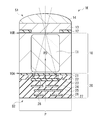
- FIG. 1 schematically shows an example of a cross-sectional configuration of an image pickup device (image pickup device 1) according to an embodiment of the present disclosure.
- FIG. 2 shows an example of the overall configuration of an image pickup device (imaging device 100) provided with the image pickup device 1 shown in FIG.
- the image pickup device 100 is, for example, a CMOS image sensor used in an electronic device such as a digital still camera or a video camera, and has a pixel portion 100A in which a plurality of pixels are two-dimensionally arranged in a matrix as an image pickup area. There is.
- the image pickup device 1 is a so-called back-illuminated image pickup device that constitutes one pixel (unit pixel P) in this CMOS image sensor or the like.
- the image pickup device 1 has a configuration in which a semiconductor substrate 10 in which a light receiving portion 11 is embedded and a multilayer wiring layer 20 having a plurality of wiring layers (for example, wiring layers 24, 25, 26) are laminated. ..
- the semiconductor substrate 10 has a first surface (front surface) 10A and a second surface (back surface) 10B facing each other.
- the multilayer wiring layer 20 is provided on the first surface 10A side of the semiconductor substrate 10, and the second surface 10B of the semiconductor substrate 10 is a light incident surface.
- the image pickup device 1 of the present embodiment has a light reflection layer 23 between the first surface 10A of the semiconductor substrate 10 and a plurality of wiring layers (wiring layers 24, 25, 26) provided in the multilayer wiring layer 20. Is provided.
- the light reflecting layer 23 is the optical of the unit pixel P in the region R in which the structure provided on the first surface 10A of the semiconductor substrate 10 is not formed in the multilayer wiring layer 20 with the interlayer insulating layer 27 in between. It forms a reflection region that is substantially symmetrical with respect to the center C1.
- the semiconductor substrate 10 corresponds to a specific example of the "semiconductor substrate” of the present disclosure
- the first surface 10A of the semiconductor substrate 10 is a specific example of the "second surface” of the present disclosure
- the second surface 10B is a specific example. It corresponds to a specific example of the "first aspect” of the present disclosure.
- the light reflecting layer 23 corresponds to a specific example of the "light reflecting layer” of the present disclosure.
- the semiconductor substrate 10 is composed of, for example, a silicon substrate. As described above, the light receiving portion 11 is embedded in the semiconductor substrate 10 for each unit pixel P, for example.
- the light receiving unit 11 is, for example, a PIN (Positive Intrinsic Negative) type photodiode PD, and has a pn junction in a predetermined region of the semiconductor substrate 10.
- PIN Positive Intrinsic Negative
- the first surface 10A of the semiconductor substrate 10 is provided with a floating diffusion FD and a pixel circuit that outputs a pixel signal based on the electric charge output from the light receiving unit 11.
- the pixel circuit has, for example, a transfer transistor TR, an amplification transistor AMP, a reset transistor RST, and a selection transistor SEL as pixel transistors.
- These floating diffusion FD, transfer transistor TR, amplification transistor AMP, reset transistor RST, and selection transistor SEL correspond to one specific example of the "structure" of the present disclosure.
- FIG. 3 shows an example of the pixel circuit of the image pickup device 1 shown in FIG.
- the transfer transistor TR is connected between the light receiving unit 11 and the floating diffusion FD.
- a drive signal TGsig is applied to the gate electrode of the transfer transistor TR.
- this drive signal TGsig becomes active, the transfer gate of the transfer transistor TR becomes conductive, and the signal charge stored in the light receiving unit 11 is transferred to the floating diffusion FD via the transfer transistor TR.
- the floating diffusion FD is connected between the transfer transistor TR and the amplification transistor AMP.
- the floating diffusion FD converts the signal charge transferred by the transfer transistor TR into a voltage signal and outputs it to the amplification transistor AMP.
- the reset transistor RST is connected between the floating diffusion FD and the power supply unit.
- a drive signal RSTsig is applied to the gate electrode of the reset transistor RST.
- this drive signal RSTsig becomes active, the reset gate of the reset transistor RST becomes conductive, and the potential of the floating diffusion FD is reset to the level of the power supply unit.
- the gate electrode of the amplification transistor AMP is connected to the floating diffusion FD, and the drain electrode is connected to the power supply unit, which serves as an input unit for a voltage signal reading circuit held by the floating diffusion FD, a so-called source follower circuit. That is, the amplification transistor AMP constitutes a constant current source and a source follower circuit connected to one end of the vertical signal line Lsig by connecting its source electrode to the vertical signal line Lsig via the selection transistor SEL.
- the selection transistor SEL is connected between the source electrode of the amplification transistor AMP and the vertical signal line Lsig.
- a drive signal SELsig is applied to the gate electrode of the selection transistor SEL.
- the selection transistor SEL becomes a conduction state, and the unit pixel P becomes a selection state.
- the read signal (pixel signal) output from the amplification transistor AMP is output to the vertical signal line Lsig via the selection transistor SEL.
- the multilayer wiring layer 20 is provided on the first surface 10A side of the semiconductor substrate 10.
- the multilayer wiring layer 20 has, for example, an insulating layer 21, a gate wiring layer 22, and an interlayer insulating layer 27 in which the light reflecting layer 23 and a plurality of wiring layers 24, 25, 26 are provided in the layer. There is.
- the insulating layer 21 is provided on the first surface 10A of the semiconductor substrate 10, for example, as a gate insulating layer of a pixel transistor.
- Examples of the material of the insulating layer 21 include silicon oxide (SiO x ), silicon nitride (SiN x ), silicon oxynitride (SiO x N y ), and the like.
- the gate wiring layer 22 is provided with, for example, the above-mentioned transfer transistor TR, amplification transistor AMP, reset transistor RST, and gate electrodes of the selection transistor SEL.
- the gate wiring layer 22 is formed by using, for example, polysilicon (Poly-Si).
- the light reflecting layer 23 passes through the semiconductor substrate 10 without being absorbed by the light receiving unit 11, reflects the light incident on the multilayer wiring layer 20, and re-enters the semiconductor substrate 10.
- the light reflecting layer 23 is provided, for example, in the interlayer insulating layer 27 between the first surface 10A of the semiconductor substrate 10 and the wiring layer 24.
- the light reflection layer 23 has only the insulating layer 21 and the interlayer insulating layer 27 sandwiched between the insulating layer 21 and the interlayer insulating layer 27 with respect to the optical center C1 of the unit pixel P. It forms a substantially symmetric reflection area.
- the substantially symmetrical points for example, the width W A of the left and right with respect to optical center C1, the case is approximately equal W B (W A ⁇ W B ).
- the optical center C1 is an axis that passes through the lens center of the on-chip lens 14, which will be described later, and the center of the opening 12H of the light-shielding film 12.
- the light reflecting layer 23 can be formed by using a material having light reflecting property.
- the material having light reflectivity include metal materials such as tungsten (W), aluminum (Al) and copper (Cu).
- the light reflecting layer 23 is also formed by using, for example, a so-called dielectric multilayer film in which layers made of an inorganic material having a high refractive index and layers made of an inorganic material having a low refractive index are alternately laminated. be able to.
- Examples of the inorganic material having a high refractive index include titanium oxide (TiO x ) and hafnium oxide (HfO x ).
- the inorganic material having a low refractive index include silicon oxide (SiO x ) and magnesium fluoride (MgF x ).
- the wiring layers 24, 25, and 26 are for, for example, driving the light receiving unit 11, transmitting signals, and applying voltage to each unit.
- the wiring layers 24, 25, and 26 are laminated in the interlayer insulating layer 27 in the order of the wiring layers 24, 25, and 26 from the semiconductor substrate 10 side, with the interlayer insulating layers 27 interposed therebetween.
- the wiring layers 24, 25, and 26 are formed of, for example, copper (Cu) or aluminum (Al).
- the interlayer insulating layer 27 is provided on the insulating layer 21 so as to cover the gate wiring layer 22, and has the light reflecting layer 23 and the wiring layers 24, 25, 26 in the layer as described above. ..
- the interlayer insulating layer 27 is formed by using, for example, silicon oxide (SiO x ), silicon nitride (SiN x ), silicon nitriding (SiO x N y ), or the like.
- a light-shielding film 12, a protective layer 13, and an on-chip lens 14 are provided on the second surface 10B side of the semiconductor substrate 10.
- the light-shielding film 12 is for preventing the oblique light incident from the light incident side S1 from being incident on the adjacent unit pixels P.
- the light-shielding film 12 is provided between adjacent unit pixels P, for example, and has an opening 12H in the center of the unit pixels P.
- the light-shielding film 12 is formed of, for example, a metal film such as tungsten (W).
- the protective layer 13 includes, for example, a light-shielding film 12 in the layer to protect the second surface 10B of the semiconductor substrate 10 and to flatten the surface of the light incident side S1.
- the protective layer 13 is formed of, for example, silicon oxide (SiO x ), silicon nitride (SiN x ), silicon oxynitride (SiO x N y ), or the like.
- the on-chip lens 14 is for condensing the light incident from the light incident side S1 on the light receiving unit 11.
- the on-chip lens 14 is formed by using a high refractive index material, and specifically, is formed of an inorganic material such as silicon oxide (SiO x ) or silicon nitride (SiN x).
- an organic material having a high refractive index such as an episulfide resin, a thietan compound or the resin thereof may be used.
- the shape of the on-chip lens 14 is not particularly limited, and various lens shapes such as a hemispherical shape and a semi-cylindrical shape can be used. As shown in FIG. 1, the on-chip lens 14 may be provided for each unit pixel P, or for example, one on-chip lens may be provided for each of a plurality of unit pixels P.
- the image pickup apparatus 100 is, for example, a CMOS image sensor, which captures incident light (image light) from a subject via an optical lens system (not shown) and pixels the amount of incident light imaged on the image pickup surface. It is converted into an electric signal in units and output as a pixel signal.
- the image pickup apparatus 100 has a pixel portion 100A as an image pickup area on the semiconductor substrate 10, and in a peripheral region of the pixel portion 100A, for example, a vertical drive circuit 111, a column signal processing circuit 112, a horizontal drive circuit 113, and an output. It has a circuit 114, a control circuit 115, and an input / output terminal 116.
- the pixel unit 100A has, for example, a plurality of unit pixels P two-dimensionally arranged in a matrix.
- a pixel drive line Lread (specifically, a row selection line and a reset control line) is wired for each pixel row, and a vertical signal line Lsig is wired for each pixel column.
- the pixel drive line Lead transmits a drive signal for reading a signal from the pixel.
- One end of the pixel drive line Lead is connected to the output end corresponding to each line of the vertical drive circuit 111.
- the vertical drive circuit 111 is configured by a shift register, an address decoder, or the like, and is a pixel drive unit that drives each unit pixel P of the pixel unit 100A, for example, in row units.
- the signal output from each unit pixel P of the pixel row selectively scanned by the vertical drive circuit 111 is supplied to the column signal processing circuit 112 through each of the vertical signal lines Lsig.
- the column signal processing circuit 112 is composed of an amplifier, a horizontal selection switch, and the like provided for each vertical signal line Lsig.
- the horizontal drive circuit 113 is composed of a shift register, an address decoder, etc., and drives each horizontal selection switch of the column signal processing circuit 112 in order while scanning. By the selective scanning by the horizontal drive circuit 113, the signals of each pixel transmitted through each of the vertical signal lines Lsig are sequentially output to the horizontal signal line 121 and transmitted to the outside of the semiconductor substrate 10 through the horizontal signal line 121. ..
- the output circuit 114 processes signals and outputs the signals sequentially supplied from each of the column signal processing groups r112 via the horizontal signal line 121.
- the output circuit 114 may, for example, perform only buffering, or may perform black level adjustment, column variation correction, various digital signal processing, and the like.
- the circuit portion including the vertical drive circuit 111, the column signal processing circuit 112, the horizontal drive circuit 113, the horizontal signal line 121, and the output circuit 114 may be formed directly on the semiconductor substrate 10, or may be used as an external control IC. It may be arranged. Further, those circuit portions may be formed on another substrate connected by a cable or the like.
- the control circuit 115 receives a clock given from the outside of the semiconductor substrate 10, data instructing an operation mode, and the like, and outputs data such as internal information of the image pickup apparatus 100.
- the control circuit 115 further has a timing generator that generates various timing signals, and the vertical drive circuit 111, the column signal processing circuit 112, the horizontal drive circuit 113, and the like based on the various timing signals generated by the timing generator. It controls the drive of peripheral circuits.
- the input / output terminal 116 exchanges signals with the outside.
- the image sensor 1 is provided on the first surface 10A of the semiconductor substrate 10 in the multilayer wiring layer 20 provided on the first surface 10A side of the semiconductor substrate 10 opposite to the light incident side S1.
- the light reflecting layer 23 is provided in the region R where the gate electrode or the like of the pixel transistor is not formed.
- the light reflecting layer 23 forms a reflecting region substantially symmetrical with respect to the optical center C1 of the unit pixel P with the insulating layer 21 and the interlayer insulating layer 27 in between.
- the light transmitted through the semiconductor substrate 10, reflected by the light reflecting layer 23, and re-entered into the light receiving portion 11 becomes substantially uniform with respect to the incident angle. This will be described below.
- the back-illuminated CIS not all the light entering from the light incident surface is photoelectrically converted in the light receiving portion, and some light is transmitted through the semiconductor substrate and provided on the side opposite to the light incident surface of the semiconductor substrate. It is incident on the multi-layered wiring layer. At that time, if there is a reflective material ahead of the light incident on the multilayer wiring layer, the light is reflected again toward the light receiving portion, so that improvement in sensitivity and suppression of color mixing are expected.
- the reflective material is formed unbalanced with respect to the optical center in the region, the light reflected by the reflective material will also have asymmetry with respect to the optical center. As described above, when the light having asymmetry re-enters the light receiving portion, the sensitivity varies greatly in the incident direction of the light, and the image quality may deteriorate.
- the present embodiment it is provided on the first surface 10A of the semiconductor substrate 10 in the multilayer wiring layer 20 provided on the first surface 10A side of the semiconductor substrate 10 opposite to the light incident side S1.
- the light reflecting layer 23 is provided in the region R where the gate electrode or the like of the pixel transistor is not formed.
- the light reflecting layer 23 forms a reflecting region substantially symmetric with respect to the optical center C1 of the unit pixel P, and has a layout having symmetry with respect to the optical center C1. As a result, the light reflected by the light reflecting layer 23 and re-entering the light receiving unit 11 becomes substantially uniform with respect to the incident angle.
- the interlayer insulating layer 27 is formed in the region R in the multilayer wiring layer 20 in which a structure such as a gate electrode (gate wiring layer 22) constituting a pixel transistor is not formed. Since the light reflecting layer 23 forming a reflection region substantially symmetric with respect to the optical center C1 of the unit pixel P is provided in between, the light is not absorbed by the light receiving unit 11 and is incident on the multilayer wiring layer 20 to emit light. The light reflected by the reflecting layer 23 and re-incidented on the light receiving portion 11 becomes substantially uniform with respect to the incident angle. As a result, the variation in sensitivity within each unit pixel P is improved, and the shading shape has a peak at the center of the angle of view. Therefore, it is possible to improve the image quality.
- a structure such as a gate electrode (gate wiring layer 22) constituting a pixel transistor
- the optical of the unit pixel P is obtained by providing the light reflecting layer 23 between the first surface 10A of the semiconductor substrate 10 and the plurality of wiring layers 24 formed in the multilayer wiring layer 20.
- An example of forming a reflection region substantially symmetric with respect to the center C1 is shown, and this reflection region is formed by any of the wiring layers 24, 25, and 26 formed by laminating the interlayer insulating layer 27 in between. May be good.
- the wiring layer 24 is substantially relative to the optical center C1 of the unit pixel P.
- the wiring layer 24 can be used as a light reflecting layer.
- the contact 24C may be formed to connect the gate wiring layer 22 and the wiring layer 24 serving as the light reflection layer.
- the contact 24C is provided in an annular shape so as to surround the region R.
- FIG. 5 schematically shows an example of the cross-sectional configuration of the image pickup device (image pickup device 1A) according to the modification 1 of the present disclosure.
- the light reflection layer 23 forming a reflection region substantially symmetrical with respect to the optical center C1 of the unit pixel P is provided, but the shape of the light reflection layer 23 is limited to this. is not it.
- the point that the light reflecting layer 33 forming a non-reflective region substantially symmetrical with respect to the optical center C1 of the unit pixel P is provided is different from the above-described embodiment.
- the light reflecting layer 33 is provided over the entire surface of the unit pixel P, for example, and has an opening 33H substantially symmetrical with respect to the optical center C1 of the unit pixel P.
- the opening 33H forms a non-reflective region substantially symmetrical with respect to the optical center C1.
- the light reflection layer 33 is formed from a region R in which structures such as a floating diffusion FD, a transfer transistor TR, an amplification transistor AMP, a reset transistor RST, and a selection transistor SEL are not formed. For example, it extends below the gate electrode of the pixel transistor.
- the substantially symmetrical points for example, the width W C of the left and right sides of the opening 33H for optical centers C1, W D is substantially equal to the case (W C ⁇ W D).
- the light reflecting layer 33 provided over the entire surface of the unit pixel P and having the opening 33H substantially symmetrical with respect to the optical center C1 of the unit pixel P is provided, so that the structure is provided.
- a non-reflective region substantially symmetric with respect to the optical center C1 is formed.
- the light that is not absorbed by the light receiving unit 11 but is incident on the multilayer wiring layer 20 and is reflected by the light reflecting layer 23 and re-incidented on the light receiving unit 11 becomes substantially uniform with respect to the incident angle.
- the variation in sensitivity within each unit pixel P is improved, and the shading shape has a peak at the center of the angle of view. Therefore, it is possible to improve the image quality.
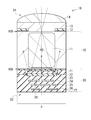
- FIG. 6 schematically shows an example of the cross-sectional configuration of the image pickup device (image pickup device 1B) according to the second modification of the present disclosure.
- the light reflecting layer 23 may form a reflection region substantially symmetric with respect to the optical center C1 of the unit pixel P with the interlayer insulating layer 27 in between, and the optical center may be formed.
- width W a of the left and right with respect to C1 if W B is met W a ⁇ W B, for example, as shown in FIG. 6, a portion of the light reflecting layer 23 extends under the gate wiring layer 22 May be.
- FIG. 7 schematically shows an example of the cross-sectional configuration of the image pickup device (image pickup device 1C) according to the third modification of the present disclosure.
- the image pickup device 1C constitutes, for example, the unit pixel P in the vicinity of the peripheral edge portion when the pupil correction is applied to the unit pixel in the vicinity of the peripheral edge portion of the pixel portion 100A in the image pickup apparatus 100 shown in FIG.
- the center of the lens of the on-chip lens 14 and the center of the opening 12H of the light-shielding film 12 are in a predetermined direction (for example, the center direction of the pixel portion 100A). It is formed at the position shifted to.
- the light reflecting layer 23 it is preferable to form the light reflecting layer 23 by shifting it in a direction opposite to the shift direction of the opening 12H of the light-shielding film 12 according to the pupil correction amount.
- the light reflecting layer 33 having the opening 33H in the direction opposite to the shift direction of the opening 12H of the light shielding film 12 according to the pupil correction amount is provided. It may be provided. As a result, the variation in sensitivity within the unit pixel P provided in the vicinity of the peripheral edge portion due to the application of the pupil correction is reduced. Therefore, it is possible to improve the image quality.
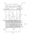
- FIG. 9 schematically shows an example of the cross-sectional configuration of the image pickup device (image pickup device 1D) according to the modified example 4 of the present disclosure.
- the structure (gate wiring layer 22) provided on the first surface 10A of the semiconductor substrate 10 is formed symmetrically with respect to the optical center C1, but will be described later, for example.
- the structure of the optical center C1 and the first surface 10A of the semiconductor substrate 10 is not formed.
- the center C2 of the region R may deviate from the center C2.
- the balance of sensitivity can be adjusted by covering the region where the sensitivity may decrease with the light reflecting layer 23. More specifically, as shown for example in FIG. 9, for example, it may be provided a light reflecting layer 23 where the width W A of the left and right with respect to optical center C1, the W B becomes W A> W B. Alternatively, for example, as shown in FIG. 10, for example, it may be provided a light reflecting layer 33 that the width W C of the left and right of the opening 33H, W D is W C ⁇ W D with respect to the optical center C1. As a result, the variation in sensitivity within the unit pixel P is reduced. Therefore, it is possible to improve the image quality.
- FIG. 11 schematically shows an example of the cross-sectional configuration of the image pickup device (image pickup device 1E) according to the modified example 5 of the present disclosure.
- the image pickup device image pickup device 1E
- the light reflecting layer 23 is selectively formed in the region where the sensitivity is low, as shown in FIG. You may do it.
- the variation in sensitivity within the unit pixel P is reduced. Therefore, it is possible to improve the image quality.
- FIG. 12 schematically shows an example of the cross-sectional configuration of the image pickup device (image pickup device 1F) according to the modification 6 of the present disclosure.
- the image sensor 1F of this modification realizes a so-called global shutter type back-illuminated CIS having, for example, a charge holding unit 15 that temporarily stores the charges generated in the light receiving unit 11 in the unit pixel P. Is.
- the global shutter method is basically a method of performing global exposure that starts exposure for all pixels at the same time and ends exposure for all pixels at the same time.
- all the pixels mean all the pixels of the portion appearing in the image, and the dummy pixels and the like are excluded.
- the global shutter method also includes a method of performing global exposure not only to all the pixels of the portion appearing in the image but also to the pixels in a predetermined region.
- FIG. 13 schematically shows an example of a specific planar configuration of the image pickup device 1F shown in FIG.
- FIG. 14 schematically shows the cross-sectional configuration of the image pickup device 1F in the I-I line shown in FIG.
- the image pickup element 1F has, as a pixel transistor, a conversion efficiency switching transistor OFG that initializes the PD, that is, resets it, in addition to the transfer transistor TR, the amplification transistor AMP, the reset transistor RST, and the selection transistor SEL. Further, for example, an element separation portion 16 is continuously formed at both ends of each gate electrode of the amplification transistor AMP, the reset transistor RST, and the selection transistor SEL and at the peripheral edge of the unit pixel P.
- the charge holding unit (MEM) 15 temporarily holds the charge generated in the light receiving unit 11 until it is transferred to the floating diffusion FD.
- the charge holding portion 15 is, for example, embedded and formed on the first surface 10A side of the semiconductor substrate 10 in the same manner as the light receiving portion 11.
- the conversion efficiency switching transistor OFG resets the PD according to the drive signal applied to the gate electrode, and has, for example, a drain connected to the power supply line VDD and a source connected to the transfer transistor TR. ing.
- the floating diffusion FD, the amplification transistor AMP, the reset transistor RST, and the selection transistor SEL are arranged in parallel along one side of the unit pixel P.
- the charge holding unit 15 is formed in the vicinity of the floating diffusion FD, for example, and the transfer transistor TR is arranged between the floating diffusion FD and the charge holding unit 15.
- the conversion efficiency switching transistor OFG is arranged on one side facing the other side in which the floating diffusion FD, the amplification transistor AMP, the reset transistor RST, and the selection transistor SEL are arranged in parallel.
- the light receiving unit 11 is formed between a floating diffusion FD, an amplification transistor AMP, a reset transistor RST, and a selection transistor SEL arranged in parallel, and a conversion efficiency switching transistor OFG.
- the light reflecting layer 23 forms a reflecting region substantially symmetrical with respect to the optical center C1 of the unit pixel P below the light receiving unit 11 as in the above embodiment.
- the light reflecting layer 23 further extends so as to cover the charge holding portion 15 in a plan view from the wiring layer side S2 side. This makes it possible to reduce the leakage of light into the charge holding unit 15, which causes a false signal (Parasitic Light Sensitivity).
- FIG. 15 schematically shows an example of a planar configuration of a non-global shutter type image sensor 1G such as the image sensor 1 that shares one pixel transistor between two adjacent unit pixels P. be.
- FIG. 16 schematically shows an example of a planar configuration of a global shutter type image sensor 1H such as the image sensor 1F that shares one pixel transistor between two adjacent unit pixels P (P1, P2). It is a representation.
- FIG. 17 schematically shows the cross-sectional configuration of the image pickup device 1H in the line II-II shown in FIG.
- the light reflection layer 23 has a mirror-symmetrical shape between adjacent unit pixels P, respectively.
- the charge holding unit MEM
- a light-shielding film is provided to suppress light leakage.
- This light-shielding film is formed of, for example, tungsten (W) and extends to the light receiving portion.
- the light-shielding film (light-shielding film 1023) has an asymmetric layout with respect to the optical center C1 including the light-receiving portion 1011.
- the width W A and the width W of the left and right of the light-shielding film 1023 with respect to the optical center C1 B and the width W A 'and width W B ' are each, for example, W a ⁇ W B, W a ' has a ⁇ W B '. Therefore, among a plurality of pixels arranged two-dimensionally in a matrix in the pixel portion, for example, an odd-numbered pixel in the row direction (for example, the unit pixel P1 in FIG. 17) and an even-numbered pixel (for example, the unit in FIG. 17). There is a variation (strength) in sensitivity between the pixel P2) and the pixel P2), which appears as vertical stripes. In addition, shading peak shift occurs in each pixel.
- the light reflection layer 23 forming a substantially symmetric reflection region is provided with respect to the optical center C1 including the light receiving portions 11 of the adjacent unit pixels P1 and P2, respectively.
- the light reflected by the light reflecting layer 23 and re-incidented into the respective light receiving portions 11 becomes substantially uniform with respect to the incident angle. Therefore, the shading shapes in the unit pixels P1 and P2 have peaks at the center of the angle of view of each other. Therefore, among the plurality of pixels two-dimensionally arranged in a matrix described above, for example, the variation in sensitivity between the odd-numbered pixel and the even-numbered pixel in the row direction is reduced. Therefore, it is possible to improve the image quality.
- FIG. 19 schematically shows an example of the cross-sectional configuration of the image pickup device (image pickup device 1I) according to the modified example 8 of the present disclosure.
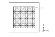
- the image pickup device 1I of this modification is different from the above-described embodiment in that the concave-convex structure 17 is provided on the first surface 10A of the semiconductor substrate 10.
- the uneven structure 17 is formed in a region R where the structure of the first surface 10A of the semiconductor substrate 10 is not formed, for example, a plurality of formed in a matrix and formed by digging in a pyramid shape. This digging is embedded, for example, by a silicon oxide (SiO x ) film 17A (see, for example, FIG. 22).
- SiO x silicon oxide
- the first surface 10A of the semiconductor substrate 10 may be formed with a concave digging substantially symmetrical with respect to the optical center C1, as shown in FIG. 21, for example.
- This concave digging is embedded by , for example, a SiO x film 17A, similar to the uneven structure 17 shown in FIG. 19 and the like.
- the light incident from the second surface 10B of the semiconductor substrate 10 and transmitted through the light receiving unit 11 is reflected toward the light receiving unit 11.
- a reflective film 17B made of a metal film or the like may be provided on the surface of the semiconductor substrate 10 on which the uneven structure 17 is formed. This improves the light reflectance on the surface of the concave-convex structure 17.
- the concave-convex structure 17 is provided on the first surface 10A of the semiconductor substrate 10, the variation in sensitivity within the unit pixel P is improved, and the shading shape has a peak in the center of the angle of view. It will be like. Further, as shown in the modification 7, the variation in sensitivity between the odd-numbered pixel and the even-numbered pixel in the image pickup element sharing one pixel transistor between two adjacent unit pixels P is reduced. .. Therefore, it is possible to improve the image quality.
- FIG. 23 schematically shows an example of the cross-sectional configuration of the image pickup device (image pickup device 1J) according to the modification 9 of the present disclosure.
- the image pickup device 1J of this modification is different from the above embodiment in that the light reflection control layers 28A and 28B having different refractive indexes are provided on the light reflection layer 23 formed in the above embodiment and the like.
- the light reflection control layer 28 (28A, 28B) can be formed, for example, by using a metamaterial composed of a single-layer film or a multilayer film using a nanostructure of a metal or a dielectric.
- FIG. 25 schematically shows an example of the cross-sectional configuration of the image pickup device (image pickup device 1K) according to the modified example 10 of the present disclosure.
- the light reflection control layer 28 is formed using a metamaterial, but the light reflection control layer 28 is formed, for example, by using a metal lens having a different refractive index in the plane. May be good.
- This makes it possible to control the light reflection direction on the surface of the light reflection layer 23, for example, as shown in FIGS. 25 and 26. Therefore, similarly to the above-mentioned modification 9, in addition to the effect of the above-described embodiment, it is possible to further improve the image quality.
- FIG. 27 schematically shows an example of the cross-sectional configuration of the image pickup device (image pickup device 1L) according to the modification 11 of the present disclosure.
- FIG. 28 schematically shows another example of the cross-sectional configuration of the image pickup device 1L according to the modified example 11 of the present disclosure.
- the image pickup element 1L of the present modification for example, a structure such as a gate electrode of a pixel transistor is formed in the multilayer wiring layer 20 provided on the first surface 10A side of the semiconductor substrate 10, as in the above embodiment.
- a light reflecting layer 43 is provided in the non-existing region R, and the surface of the semiconductor substrate 10 facing the first surface 10A is substantially symmetric or asymmetric with respect to the optical center C1 as shown in FIGS. 27 and 28, for example. It differs from the above-described embodiment in that an uneven structure and a step are provided.
- the light reflecting layer 23 is formed by using a metal material such as tungsten (W) or a dielectric multilayer film
- the light reflecting layer 43 constitutes the interlayer insulating layer 27. It may be formed by using an insulating material having a refractive index different from that of the insulating material. Even in the light reflecting layer 43 formed by using the insulating material, it is possible to control the light reflecting direction on the surface thereof.
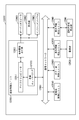
- FIG. 29 shows an example of a schematic configuration of an image pickup system 2 provided with an image pickup device (for example, an image pickup device 1) according to the above-described embodiment and modifications 1 to 11.
- an image pickup device for example, an image pickup device 1
- the image pickup system 2 is, for example, an image pickup device such as a digital still camera or a video camera, or an electronic device such as a mobile terminal device such as a smartphone or a tablet terminal.
- the image pickup system 2 includes, for example, an image pickup element 1, an optical system 241, a shutter device 242, a DSP circuit 243, a frame memory 244, a display unit 245, a storage unit 246, an operation unit 247, and a power supply unit 248.
- the image pickup element 1, the DSP circuit 243, the frame memory 244, the display unit 245, the storage unit 246, the operation unit 247, and the power supply unit 248 are connected to each other via a bus line 249.
- the image sensor 1 outputs image data according to the incident light.
- the optical system 241 is configured to have one or a plurality of lenses, and guides light (incident light) from a subject to an image pickup element 1 to form an image on a light receiving surface of the image pickup element 1.
- the shutter device 242 is arranged between the optical system 241 and the image pickup element 1, and controls the light irradiation period and the light shielding period to the image pickup element 1 according to the control of the drive circuit.
- the DSP circuit 243 is a signal processing circuit that processes a signal (image data) output from the image sensor 1.
- the frame memory 244 temporarily holds the image data processed by the DSP circuit 243 in frame units.
- the display unit 245 comprises a panel-type display device such as a liquid crystal panel or an organic EL (ElectroLuminescence) panel, and displays a moving image or a still image captured by the image pickup device 1.
- the storage unit 246 records image data of a moving image or a still image captured by the image pickup device 1 on a recording medium such as a semiconductor memory or a hard disk.
- the operation unit 247 issues operation commands for various functions of the image pickup system 2 according to the operation by the user.
- the power supply unit 248 appropriately supplies various power sources that serve as operating power sources for the image pickup element 1, the DSP circuit 243, the frame memory 244, the display unit 245, the storage unit 246, and the operation unit 247.
- FIG. 30 shows an example of a flowchart of an imaging operation in the imaging system 2.
- the user instructs the start of imaging by operating the operation unit 247 (step S101).
- the operation unit 247 transmits an image pickup command to the image pickup element 1 (step S102).
- the image pickup element 1 (specifically, the system control circuit) executes an image pickup by a predetermined image pickup method (step S103).
- the image sensor 1 outputs the image data obtained by the image pickup to the DSP circuit 243.
- the image data is data for all pixels of the pixel signal generated based on the electric charge temporarily held in the floating diffusion FD.
- the DSP circuit 243 performs predetermined signal processing (for example, noise reduction processing) based on the image data input from the image sensor 1 (step S104).
- the DSP circuit 243 stores the image data to which the predetermined signal processing has been performed in the frame memory 244, and the frame memory 244 stores the image data in the storage unit 246 (step S105). In this way, the image pickup in the image pickup system 2 is performed.
- the image pickup devices 1, 1A to 1F according to the above-described embodiment and modifications 1 to 6 are applied to the image pickup system 2.
- the image sensor 1 can be miniaturized or high-definition, so that a small-sized or high-definition image pickup system 2 can be provided.
- the technology according to the present disclosure can be applied to various products.
- the technology according to the present disclosure is realized as a device mounted on a moving body of any kind such as an automobile, an electric vehicle, a hybrid electric vehicle, a motorcycle, a bicycle, a personal mobility, an airplane, a drone, a ship, and a robot. You may.
- FIG. 31 is a block diagram showing a schematic configuration example of a vehicle control system, which is an example of a mobile control system to which the technique according to the present disclosure can be applied.
- the vehicle control system 12000 includes a plurality of electronic control units connected via the communication network 12001.
- the vehicle control system 12000 includes a drive system control unit 12010, a body system control unit 12020, an outside information detection unit 12030, an in-vehicle information detection unit 12040, and an integrated control unit 12050.
- a microcomputer 12051, an audio image output unit 12052, and an in-vehicle network I / F (interface) 12053 are shown as a functional configuration of the integrated control unit 12050.
- the drive system control unit 12010 controls the operation of the device related to the drive system of the vehicle according to various programs.
- the drive system control unit 12010 has a driving force generator for generating the driving force of the vehicle such as an internal combustion engine or a driving motor, a driving force transmission mechanism for transmitting the driving force to the wheels, and a steering angle of the vehicle. It functions as a control device such as a steering mechanism for adjusting and a braking device for generating braking force of the vehicle.
- the body system control unit 12020 controls the operation of various devices mounted on the vehicle body according to various programs.
- the body system control unit 12020 functions as a keyless entry system, a smart key system, a power window device, or a control device for various lamps such as headlamps, back lamps, brake lamps, turn signals or fog lamps.
- the body system control unit 12020 may be input with radio waves transmitted from a portable device that substitutes for the key or signals of various switches.
- the body system control unit 12020 receives inputs of these radio waves or signals and controls a vehicle door lock device, a power window device, a lamp, and the like.
- the outside information detection unit 12030 detects information outside the vehicle equipped with the vehicle control system 12000.
- the image pickup unit 12031 is connected to the vehicle outside information detection unit 12030.
- the vehicle outside information detection unit 12030 causes the image pickup unit 12031 to capture an image of the outside of the vehicle and receives the captured image.
- the vehicle outside information detection unit 12030 may perform object detection processing or distance detection processing such as a person, a vehicle, an obstacle, a sign, or a character on the road surface based on the received image.
- the image pickup unit 12031 is an optical sensor that receives light and outputs an electric signal according to the amount of the light received.
- the image pickup unit 12031 can output an electric signal as an image or can output it as distance measurement information. Further, the light received by the image pickup unit 12031 may be visible light or invisible light such as infrared light.
- the in-vehicle information detection unit 12040 detects the in-vehicle information.
- a driver state detection unit 12041 that detects the state of the driver is connected to the in-vehicle information detection unit 12040.
- the driver state detection unit 12041 includes, for example, a camera that images the driver, and the in-vehicle information detection unit 12040 determines the degree of fatigue or concentration of the driver based on the detection information input from the driver state detection unit 12041. It may be calculated, or it may be determined whether the driver has fallen asleep.
- the microcomputer 12051 calculates the control target value of the driving force generator, the steering mechanism, or the braking device based on the information inside and outside the vehicle acquired by the vehicle exterior information detection unit 12030 or the vehicle interior information detection unit 12040, and the drive system control unit.
- a control command can be output to 12010.
- the microcomputer 12051 realizes ADAS (Advanced Driver Assistance System) functions including vehicle collision avoidance or impact mitigation, follow-up driving based on inter-vehicle distance, vehicle speed maintenance driving, vehicle collision warning, vehicle lane deviation warning, and the like. It is possible to perform cooperative control for the purpose of.
- ADAS Advanced Driver Assistance System
- the microcomputer 12051 controls the driving force generating device, the steering mechanism, the braking device, and the like based on the information around the vehicle acquired by the vehicle exterior information detection unit 12030 or the vehicle interior information detection unit 12040. It is possible to perform coordinated control for the purpose of automatic driving that runs autonomously without depending on the operation.
- the microcomputer 12051 can output a control command to the body system control unit 12020 based on the information outside the vehicle acquired by the vehicle outside information detection unit 12030.
- the microcomputer 12051 controls the headlamps according to the position of the preceding vehicle or the oncoming vehicle detected by the outside information detection unit 12030, and performs cooperative control for the purpose of anti-glare such as switching the high beam to the low beam. It can be carried out.
- the audio image output unit 12052 transmits an output signal of at least one of audio and an image to an output device capable of visually or audibly notifying information to the passenger or the outside of the vehicle.
- an audio speaker 12061, a display unit 12062, and an instrument panel 12063 are exemplified as output devices.
- the display unit 12062 may include, for example, at least one of an onboard display and a head-up display.
- FIG. 32 is a diagram showing an example of the installation position of the image pickup unit 12031.
- the vehicle 12100 has an imaging unit 12101, 12102, 12103, 12104, 12105 as an imaging unit 12031.
- the image pickup units 12101, 12102, 12103, 12104, 12105 are provided, for example, at positions such as the front nose, side mirrors, rear bumpers, back doors, and the upper part of the windshield in the vehicle interior of the vehicle 12100.
- the image pickup unit 12101 provided in the front nose and the image pickup section 12105 provided in the upper part of the windshield in the vehicle interior mainly acquire an image in front of the vehicle 12100.
- the image pickup units 12102 and 12103 provided in the side mirror mainly acquire images of the side of the vehicle 12100.
- the image pickup unit 12104 provided in the rear bumper or the back door mainly acquires an image of the rear of the vehicle 12100.
- the images in front acquired by the image pickup units 12101 and 12105 are mainly used for detecting a preceding vehicle, a pedestrian, an obstacle, a traffic light, a traffic sign, a lane, or the like.
- FIG. 32 shows an example of the shooting range of the imaging units 12101 to 12104.
- the imaging range 12111 indicates the imaging range of the imaging unit 12101 provided on the front nose
- the imaging ranges 12112 and 12113 indicate the imaging range of the imaging units 12102 and 12103 provided on the side mirrors, respectively
- the imaging range 12114 indicates the imaging range.
- the imaging range of the imaging unit 12104 provided on the rear bumper or the back door is shown. For example, by superimposing the image data captured by the image pickup units 12101 to 12104, a bird's-eye view image of the vehicle 12100 can be obtained.
- At least one of the image pickup units 12101 to 12104 may have a function of acquiring distance information.
- at least one of the image pickup units 12101 to 12104 may be a stereo camera including a plurality of image pickup elements, or may be an image pickup element having pixels for phase difference detection.
- the microcomputer 12051 has a distance to each three-dimensional object in the image pickup range 12111 to 12114 based on the distance information obtained from the image pickup unit 12101 to 12104, and a temporal change of this distance (relative speed with respect to the vehicle 12100). By obtaining can. Further, the microcomputer 12051 can set an inter-vehicle distance to be secured in advance in front of the preceding vehicle, and can perform automatic brake control (including follow-up stop control), automatic acceleration control (including follow-up start control), and the like. In this way, it is possible to perform coordinated control for the purpose of automatic driving or the like in which the vehicle travels autonomously without depending on the operation of the driver.
- automatic brake control including follow-up stop control
- automatic acceleration control including follow-up start control
- the microcomputer 12051 converts three-dimensional object data related to a three-dimensional object into two-wheeled vehicles, ordinary vehicles, large vehicles, pedestrians, electric poles, and other three-dimensional objects based on the distance information obtained from the image pickup units 12101 to 12104. It can be classified and extracted and used for automatic avoidance of obstacles. For example, the microcomputer 12051 distinguishes obstacles around the vehicle 12100 into obstacles that are visible to the driver of the vehicle 12100 and obstacles that are difficult to see. Then, the microcomputer 12051 determines the collision risk indicating the risk of collision with each obstacle, and when the collision risk is equal to or higher than the set value and there is a possibility of collision, the microcomputer 12051 via the audio speaker 12061 or the display unit 12062. By outputting an alarm to the driver and performing forced deceleration and avoidance steering via the drive system control unit 12010, driving support for collision avoidance can be provided.
- At least one of the image pickup units 12101 to 12104 may be an infrared camera that detects infrared rays.
- the microcomputer 12051 can recognize a pedestrian by determining whether or not a pedestrian is present in the captured image of the imaging unit 12101 to 12104.
- pedestrian recognition is, for example, a procedure for extracting feature points in an image captured by an image pickup unit 12101 to 12104 as an infrared camera, and pattern matching processing is performed on a series of feature points indicating the outline of an object to determine whether or not the pedestrian is a pedestrian. It is done by the procedure to determine.
- the audio image output unit 12052 determines the square contour line for emphasizing the recognized pedestrian.
- the display unit 12062 is controlled so as to superimpose and display. Further, the audio image output unit 12052 may control the display unit 12062 so as to display an icon or the like indicating a pedestrian at a desired position.
- the above is an example of a mobile control system to which the technology according to the present disclosure can be applied.
- the technique according to the present disclosure can be applied to the image pickup unit 12031 among the configurations described above.
- the image pickup apparatus 100 can be applied to the image pickup unit 12031.
- the technique according to the present disclosure it is possible to obtain a high-definition photographed image with less noise, so that high-precision control using the photographed image can be performed in the moving body control system.
- the technology according to the present disclosure (the present technology) can be applied to various products.
- the techniques according to the present disclosure may be applied to an endoscopic surgery system.
- FIG. 33 is a diagram showing an example of a schematic configuration of an endoscopic surgery system to which the technique according to the present disclosure (the present technique) can be applied.
- FIG. 33 illustrates how the surgeon (doctor) 11131 is performing surgery on patient 11132 on patient bed 11153 using the endoscopic surgery system 11000.
- the endoscopic surgery system 11000 includes an endoscope 11100, other surgical tools 11110 such as an abdominal tube 11111 and an energy treatment tool 11112, and a support arm device 11120 that supports the endoscope 11100.
- a cart 11200 equipped with various devices for endoscopic surgery.
- the endoscope 11100 is composed of a lens barrel 11101 in which a region having a predetermined length from the tip is inserted into the body cavity of the patient 11132, and a camera head 11102 connected to the base end of the lens barrel 11101.
- the endoscope 11100 configured as a so-called rigid mirror having a rigid barrel 11101 is illustrated, but the endoscope 11100 may be configured as a so-called flexible mirror having a flexible barrel. good.
- An opening in which an objective lens is fitted is provided at the tip of the lens barrel 11101.
- a light source device 11203 is connected to the endoscope 11100, and the light generated by the light source device 11203 is guided to the tip of the lens barrel by a light guide extending inside the lens barrel 11101, and is an objective. It is irradiated toward the observation target in the body cavity of the patient 11132 through the lens.
- the endoscope 11100 may be a direct endoscope, a perspective mirror, or a side endoscope.
- An optical system and an image pickup element are provided inside the camera head 11102, and the reflected light (observation light) from the observation target is focused on the image pickup element by the optical system.
- the observation light is photoelectrically converted by the image pickup device, and an electric signal corresponding to the observation light, that is, an image signal corresponding to the observation image is generated.
- the image signal is transmitted as RAW data to the camera control unit (CCU: Camera Control Unit) 11201.
- the CCU11201 is composed of a CPU (Central Processing Unit), a GPU (Graphics Processing Unit), and the like, and comprehensively controls the operations of the endoscope 11100 and the display device 11202. Further, the CCU11201 receives an image signal from the camera head 11102, and performs various image processing on the image signal for displaying an image based on the image signal, such as development processing (demosaic processing).
- a CPU Central Processing Unit
- GPU Graphics Processing Unit
- the display device 11202 displays an image based on the image signal processed by the CCU 11201 under the control of the CCU 11201.
- the light source device 11203 is composed of, for example, a light source such as an LED (Light Emitting Diode), and supplies irradiation light for photographing an operating part or the like to the endoscope 11100.
- a light source such as an LED (Light Emitting Diode)
- LED Light Emitting Diode
- the input device 11204 is an input interface for the endoscopic surgery system 11000.
- the user can input various information and input instructions to the endoscopic surgery system 11000 via the input device 11204.
- the user inputs an instruction to change the imaging conditions (type of irradiation light, magnification, focal length, etc.) by the endoscope 11100.
- the treatment tool control device 11205 controls the drive of the energy treatment tool 11112 for cauterizing, incising, sealing a blood vessel, or the like of a tissue.
- the pneumoperitoneum device 11206 uses a gas in the pneumoperitoneum tube 11111 to inflate the body cavity of the patient 11132 for the purpose of securing the field of view by the endoscope 11100 and securing the work space of the operator. Is sent.
- the recorder 11207 is a device capable of recording various information related to surgery.
- the printer 11208 is a device capable of printing various information related to surgery in various formats such as text, images, and graphs.
- the light source device 11203 that supplies the irradiation light to the endoscope 11100 when photographing the surgical site can be composed of, for example, an LED, a laser light source, or a white light source composed of a combination thereof.
- a white light source is configured by a combination of RGB laser light sources, the output intensity and output timing of each color (each wavelength) can be controlled with high accuracy. Therefore, the light source device 11203 adjusts the white balance of the captured image. It can be carried out.
- the laser light from each of the RGB laser light sources is irradiated to the observation target in a time-division manner, and the drive of the image sensor of the camera head 11102 is controlled in synchronization with the irradiation timing to correspond to each of RGB. It is also possible to capture the image in a time-division manner. According to this method, a color image can be obtained without providing a color filter in the image pickup device.
- the drive of the light source device 11203 may be controlled so as to change the intensity of the output light at predetermined time intervals.
- the drive of the image sensor of the camera head 11102 in synchronization with the timing of the change of the light intensity to acquire an image in time division and synthesizing the image, so-called high dynamic without blackout and overexposure. Range images can be generated.
- the light source device 11203 may be configured to be able to supply light in a predetermined wavelength band corresponding to special light observation.
- special light observation for example, by utilizing the wavelength dependence of light absorption in body tissue, the surface layer of the mucous membrane is irradiated with light in a narrower band than the irradiation light (that is, white light) during normal observation.
- a so-called narrow band imaging is performed in which a predetermined tissue such as a blood vessel is photographed with high contrast.
- fluorescence observation may be performed in which an image is obtained by fluorescence generated by irradiating with excitation light.
- the body tissue is irradiated with excitation light to observe the fluorescence from the body tissue (autofluorescence observation), or a reagent such as indocyanine green (ICG) is locally injected into the body tissue and the body tissue is injected. It is possible to obtain a fluorescence image by irradiating the excitation light corresponding to the fluorescence wavelength of the reagent.
- the light source device 11203 may be configured to be capable of supplying narrowband light and / or excitation light corresponding to such special light observation.
- FIG. 34 is a block diagram showing an example of the functional configuration of the camera head 11102 and CCU11201 shown in FIG. 33.
- the camera head 11102 includes a lens unit 11401, an image pickup unit 11402, a drive unit 11403, a communication unit 11404, and a camera head control unit 11405.
- CCU11201 has a communication unit 11411, an image processing unit 11412, and a control unit 11413.
- the camera head 11102 and CCU11201 are communicably connected to each other by a transmission cable 11400.
- the lens unit 11401 is an optical system provided at a connection portion with the lens barrel 11101.
- the observation light taken in from the tip of the lens barrel 11101 is guided to the camera head 11102 and incident on the lens unit 11401.
- the lens unit 11401 is configured by combining a plurality of lenses including a zoom lens and a focus lens.
- the image pickup unit 11402 is composed of an image pickup element.
- the image pickup element constituting the image pickup unit 11402 may be one (so-called single plate type) or a plurality (so-called multi-plate type).
- each image pickup element may generate an image signal corresponding to each of RGB, and a color image may be obtained by synthesizing them.
- the image pickup unit 11402 may be configured to have a pair of image pickup elements for acquiring image signals for the right eye and the left eye corresponding to 3D (Dimensional) display, respectively.
- the 3D display enables the operator 11131 to more accurately grasp the depth of the living tissue in the surgical site.
- a plurality of lens units 11401 may be provided corresponding to each image pickup element.
- the image pickup unit 11402 does not necessarily have to be provided on the camera head 11102.
- the image pickup unit 11402 may be provided inside the lens barrel 11101 immediately after the objective lens.
- the drive unit 11403 is composed of an actuator, and the zoom lens and focus lens of the lens unit 11401 are moved by a predetermined distance along the optical axis under the control of the camera head control unit 11405. As a result, the magnification and focus of the image captured by the image pickup unit 11402 can be adjusted as appropriate.
- the communication unit 11404 is configured by a communication device for transmitting and receiving various information to and from the CCU11201.
- the communication unit 11404 transmits the image signal obtained from the image pickup unit 11402 as RAW data to the CCU 11201 via the transmission cable 11400.
- the communication unit 11404 receives a control signal for controlling the drive of the camera head 11102 from the CCU 11201 and supplies the control signal to the camera head control unit 11405.
- the control signal includes, for example, information to specify the frame rate of the captured image, information to specify the exposure value at the time of imaging, and / or information to specify the magnification and focus of the captured image. Contains information about the condition.
- the image pickup conditions such as the frame rate, exposure value, magnification, and focus may be appropriately specified by the user, or may be automatically set by the control unit 11413 of CCU11201 based on the acquired image signal. good.
- the endoscope 11100 is equipped with a so-called AE (Auto Exposure) function, an AF (Auto Focus) function, and an AWB (Auto White Balance) function.
- the camera head control unit 11405 controls the drive of the camera head 11102 based on the control signal from the CCU 11201 received via the communication unit 11404.
- the communication unit 11411 is configured by a communication device for transmitting and receiving various information to and from the camera head 11102.
- the communication unit 11411 receives an image signal transmitted from the camera head 11102 via the transmission cable 11400.
- the communication unit 11411 transmits a control signal for controlling the drive of the camera head 11102 to the camera head 11102.
- Image signals and control signals can be transmitted by telecommunications, optical communication, or the like.
- the image processing unit 11412 performs various image processing on the image signal which is the RAW data transmitted from the camera head 11102.
- the control unit 11413 performs various controls related to the imaging of the surgical site and the like by the endoscope 11100 and the display of the captured image obtained by the imaging of the surgical site and the like. For example, the control unit 11413 generates a control signal for controlling the drive of the camera head 11102.
- control unit 11413 causes the display device 11202 to display an image captured by the surgical unit or the like based on the image signal processed by the image processing unit 11412.
- the control unit 11413 may recognize various objects in the captured image by using various image recognition techniques.
- the control unit 11413 detects a surgical tool such as forceps, a specific biological part, bleeding, mist when using the energy treatment tool 11112, etc. by detecting the shape, color, etc. of the edge of the object included in the captured image. Can be recognized.
- the control unit 11413 may superimpose and display various surgical support information on the image of the surgical unit by using the recognition result. By superimposing and displaying the surgical support information and presenting it to the surgeon 11131, the burden on the surgeon 11131 can be reduced and the surgeon 11131 can surely proceed with the surgery.
- the transmission cable 11400 connecting the camera head 11102 and CCU11201 is an electric signal cable corresponding to electric signal communication, an optical fiber corresponding to optical communication, or a composite cable thereof.
- the communication is performed by wire using the transmission cable 11400, but the communication between the camera head 11102 and the CCU11201 may be performed wirelessly.
- the above is an example of an endoscopic surgery system to which the technology according to the present disclosure can be applied.
- the technique according to the present disclosure can be suitably applied to the image pickup unit 11402 provided in the camera head 11102 of the endoscope 11100 among the configurations described above.
- the image pickup unit 11402 can be miniaturized or high-definition, so that a small-sized or high-definition endoscope 11100 can be provided.
- the present disclosure has been described above with reference to embodiments and modifications 1 to 11 as well as application examples and application examples, the present disclosure is not limited to the above-described embodiments and the like, and various modifications are possible. ..
- a red filter that transmits light in the red wavelength region
- a green filter that transmits light in the green wavelength region
- a blue color that transmits light in the blue wavelength region.
- the filter may be provided with an optical member such as a color filter provided in a regular color arrangement (for example, a bayer arrangement) in the pixel portion 100A, for example.
- the present disclosure may also have the following structure. According to the present technology having the following configuration, it is provided on the second surface side having a plurality of structures opposite to the first surface which is the light incident surface of the first semiconductor substrate having a light receiving portion for each pixel.
- a light-reflecting layer having a reflective region substantially symmetric or a non-reflective region substantially symmetric with respect to the optical center of the pixel is provided between the interlayer insulating layers in the region where the structure is not formed. I tried to provide it. As a result, the light reflected by the light reflecting layer and re-entering the light receiving portion becomes substantially uniform with respect to the incident angle. Therefore, it is possible to improve the image quality.
- a semiconductor substrate having a first surface to be a light incident surface and a second surface opposite to the first surface, and also having a light receiving portion that generates a charge corresponding to the amount of received light for each pixel by photoelectric conversion.
- a multilayer wiring layer provided on the second surface side of the semiconductor substrate and having a plurality of wiring layers laminated between the interlayer insulating layers.
- a plurality of structures provided on the second surface of the semiconductor substrate, and In the region provided in the multilayer wiring layer where the structure is not formed, a reflective region substantially symmetric or a non-reflective region substantially symmetric with respect to the optical center of the pixel is formed with the interlayer insulating layer in between.
- An image sensor with a light-reflecting layer.
- the image pickup device includes a floating diffusion that converts a signal charge generated in the light receiving unit into a voltage signal, a transfer transistor that transfers the signal charge generated in the light receiving unit to the floating diffusion, and the floating diffusion.
- a reset transistor that resets the potential of the voltage signal to a predetermined potential
- an amplification transistor that is an input unit of the voltage signal held by the floating diffusion
- a selection transistor that controls the output timing of the voltage signal from the amplification transistor.
- the imaging device according to any one of (1) to (8).
- the image pickup device (10) The image pickup device according to (8) or (9), wherein the plurality of structures are provided for each pixel and further have a charge holding portion for accumulating the charge generated in the light receiving portion.
- the light reflecting layer has a concavo-convex structure on a surface facing the second surface of the semiconductor substrate.
- the uneven structure has a shape substantially symmetrical with respect to the optical center.
- the image pickup device according to any one of (1) to (12), further having a light reflection control layer having a different in-plane refractive index on the second surface of the semiconductor substrate.
- the light reflecting layer is composed of a metal lens.
- the semiconductor substrate has a curved surface portion substantially symmetrical with respect to the optical center as the concave-convex structure.
- a reflective film is formed on the surface of the uneven structure.
- the image pickup device according to any one of (1) to (18) above, which is formed as described above. (20) The image pickup device according to any one of (1) to (19), wherein the light reflecting layer is formed of a metal material. (21) The image pickup device according to any one of (1) to (20) above, wherein the light reflecting layer is formed by using a dielectric multilayer film.
- the light reflecting layer is formed by the wiring layer provided on the second surface side of the semiconductor substrate among the plurality of wiring layers in which the interlayer insulating layer is laminated.
- the image pickup device according to any one of (21).
- a semiconductor substrate having a first surface to be a light incident surface and a second surface opposite to the first surface, and also having a light receiving portion that generates a charge corresponding to the amount of received light for each pixel by photoelectric conversion.
- a multilayer wiring layer provided on the second surface side of the semiconductor substrate and having a plurality of wiring layers laminated between the interlayer insulating layers.
- a plurality of structures provided on the second surface of the semiconductor substrate In the region provided in the multilayer wiring layer where the structure is not formed, a reflective region substantially symmetric or a non-reflective region substantially symmetric with respect to the optical center of the pixel is formed with the interlayer insulating layer in between.
- An image pickup device having an image pickup element provided with a light-reflecting layer.
Landscapes
- Engineering & Computer Science (AREA)
- Physics & Mathematics (AREA)
- Power Engineering (AREA)
- Electromagnetism (AREA)
- Condensed Matter Physics & Semiconductors (AREA)
- General Physics & Mathematics (AREA)
- Computer Hardware Design (AREA)
- Microelectronics & Electronic Packaging (AREA)
- Multimedia (AREA)
- Signal Processing (AREA)
- Solid State Image Pick-Up Elements (AREA)
Abstract
本開示の一実施形態の撮像素子は、光入射面となる第1の面と、第1の面の反対側の第2の面を有すると共に、画素毎に受光量に応じた電荷を光電変換により生成する受光部を有する半導体基板と、半導体基板の第2の面側に設けられると共に、層間絶縁層を間に複数の配線層が積層されている多層配線層と、多層配線層内において、半導体基板の第2の面に設けられた複数の構造物と、多層配線層内に設けられ、構造物が形成されていない領域において、層間絶縁層を間にして画素の光学中心に対して略対称な反射領域または略対称な非反射領域を形成する光反射層とを備える。
Description
本開示は、例えば裏面照射型の撮像素子およびこれを備えた撮像装置に関する。
裏面照射型のCMOS(Complementary Metal Oxide Semiconductor)イメージセンサ(CIS)では、受光部において吸収されずに透過した光は、受光部の下方に設けられた配線層(金属層)によって反射されて受光部に再入射することがある。この反射光の強度が画素毎に不均一である場合、隣り合う画素間において光学的混色が発生する。これに対して、例えば、特許文献1では、受光部の下方に、各画素に対して一様な第1の反射板および隣り合う画素間に第2の反射板を周期的に設けることで画質の向上を図った固体撮像装置が開示されている。
このように、撮像装置では画質の向上が求められている。
画質を向上させることが可能な撮像素子および撮像装置を提供することが望ましい。
本開示の一実施形態としての撮像素子は、光入射面となる第1の面と、第1の面の反対側の第2の面を有すると共に、画素毎に受光量に応じた電荷を光電変換により生成する受光部を有する半導体基板と、半導体基板の第2の面側に設けられると共に、層間絶縁層を間に複数の配線層が積層されている多層配線層と、多層配線層内において、半導体基板の第2の面に設けられた複数の構造物と、多層配線層内に設けられ、構造物が形成されていない領域において、層間絶縁層を間にして画素の光学中心に対して略対称な反射領域または略対称な非反射領域を形成する光反射層とを備えたものである。
本開示の一実施形態としての撮像装置は、上記本開示の一実施形態の撮像素子を備えたものである。
本開示の一実施形態としての撮像素子および一実施形態の撮像装置では、画素毎に受光部を有する第1の半導体基板の光入射面となる第1の面とは反対の、複数の構造物を有する第2の面側に設けられた多層配線層内に、光反射層を設けるようにした。この光反射層は、構造物が形成されていない領域において、層間絶縁層を間にして画素の光学中心に対して略対称な反射領域または略対称な非反射領域を形成している。これにより、光反射層によって反射され受光部に再入射する光が入射角に対して略均一となる。
以下、本開示における一実施形態について、図面を参照して詳細に説明する。以下の説明は本開示の一具体例であって、本開示は以下の態様に限定されるものではない。また、本開示は、各図に示す各構成要素の配置や寸法、寸法比等についても、それらに限定されるものではない。なお、説明する順序は、下記の通りである。
1.実施の形態(半導体基板の表面と多層配線層内における複数の配線層との間に、光学中心に対して対称な光反射層を設けた例)
1-1.撮像素子の構成
1-2.撮像装置の構成
1-3.作用・効果
2.変形例
2-1.変形例1(光学中心に対して対称な開口部を有する光反射層を設けた例)
2-2.変形例2(光反射層の形状の他の例)
2-3.変形例3(周辺部における光反射層の形成位置の例)
2-4.変形例4(光反射層の形成位置の他の例)
2-5.変形例5(光反射層の形成位置の他の例)
2-6.変形例6(電荷保持部を備えた撮像素子の例)
2-7.変形例7(隣り合う画素間で読み出し回路を共有する撮像素子の例)
2-8.変形例8(半導体基板の表面に凹凸構造を設けた例)
2-9.変形例9(光反射層上に光反射制御層をさらに設けた例)
2-10.変形例10(光反射制御層の他の例)
2-11.変形例11(光反射層の他の例)
3.適用例
4.応用例
<1.実施の形態>
図1は、本開示の一実施の形態に係る撮像素子(撮像素子1)の断面構成の一例を模式的に表したものである。図2は、図1に示した撮像素子1を備えた撮像装置(撮像装置100)の全体構成の一例を表したものである。撮像装置100は、例えば、デジタルスチルカメラ、ビデオカメラ等の電子機器に用いられるCMOSイメージセンサ等であり、撮像エリアとして、複数の画素が行列状に2次元配置された画素部100Aを有している。撮像素子1は、このCMOSイメージセンサ等において、1つの画素(単位画素P)を構成する所謂裏面照射型の撮像素子である。
図1は、本開示の一実施の形態に係る撮像素子(撮像素子1)の断面構成の一例を模式的に表したものである。図2は、図1に示した撮像素子1を備えた撮像装置(撮像装置100)の全体構成の一例を表したものである。撮像装置100は、例えば、デジタルスチルカメラ、ビデオカメラ等の電子機器に用いられるCMOSイメージセンサ等であり、撮像エリアとして、複数の画素が行列状に2次元配置された画素部100Aを有している。撮像素子1は、このCMOSイメージセンサ等において、1つの画素(単位画素P)を構成する所謂裏面照射型の撮像素子である。
(1-1.撮像素子の構成)
撮像素子1は、受光部11が埋め込み形成された半導体基板10と、複数の配線層(例えば、配線層24,25,26)を有する多層配線層20とが積層された構成を有している。半導体基板10は、対向する第1面(表面)10Aおよび第2面(裏面)10Bを有している。多層配線層20は、半導体基板10の第1面10A側に設けられており、半導体基板10の第2面10Bは光入射面となっている。本実施の形態の撮像素子1は、半導体基板10の第1面10Aと、多層配線層20内に設けられた複数の配線層(配線層24,25,26)との間に光反射層23が設けられたものである。この光反射層23は、多層配線層20内において、半導体基板10の第1面10Aに設けられた構造物が形成されていない領域Rにおいて、層間絶縁層27を間にして単位画素Pの光学中心C1に対して略対称な反射領域を形成するものである。
撮像素子1は、受光部11が埋め込み形成された半導体基板10と、複数の配線層(例えば、配線層24,25,26)を有する多層配線層20とが積層された構成を有している。半導体基板10は、対向する第1面(表面)10Aおよび第2面(裏面)10Bを有している。多層配線層20は、半導体基板10の第1面10A側に設けられており、半導体基板10の第2面10Bは光入射面となっている。本実施の形態の撮像素子1は、半導体基板10の第1面10Aと、多層配線層20内に設けられた複数の配線層(配線層24,25,26)との間に光反射層23が設けられたものである。この光反射層23は、多層配線層20内において、半導体基板10の第1面10Aに設けられた構造物が形成されていない領域Rにおいて、層間絶縁層27を間にして単位画素Pの光学中心C1に対して略対称な反射領域を形成するものである。
この半導体基板10が、本開示の「半導体基板」の一具体例に相当し、半導体基板10の第1面10Aが本開示の「第2の面」の一具体例に、第2面10Bが本開示の「第1の面」の一具体例に相当する。光反射層23が、本開示の「光反射層」の一具体例に相当する。
半導体基板10は、例えば、シリコン基板で構成されている。半導体基板10には、上記のように、受光部11が、例えば単位画素P毎に埋め込み形成されている。この受光部11は、例えばPIN(Positive Intrinsic Negative)型のフォトダイオードPDであり、半導体基板10の所定領域にpn接合を有している。
半導体基板10の第1面10Aには、フローティングディフュージョンFDや、受光部11から出力された電荷に基づく画素信号を出力する画素回路が設けられている。画素回路は、画素トランジスタとして、例えば、転送トランジスタTR、増幅トランジスタAMP、リセットトランジスタRSTおよび選択トランジスタSELを有している。これらフローティングディフュージョンFD、転送トランジスタTR、増幅トランジスタAMP、リセットトランジスタRSTおよび選択トランジスタSELが、本開示の「構造物」の一具体例に相当する。
図3は、図1に示した撮像素子1の画素回路の一例を表したものである。
転送トランジスタTRは、受光部11とフローティングディフュージョンFDとの間に接続されている。転送トランジスタTRのゲート電極には、駆動信号TGsigが印加される。この駆動信号TGsigがアクティブ状態になると、転送トランジスタTRの転送ゲートが導通状態となり、受光部11に蓄積されている信号電荷が、転送トランジスタTRを介してフローティングディフュージョンFDに転送される。
フローティングディフュージョンFDは、転送トランジスタTRと増幅トランジスタAMPとの間に接続されている。フローティングディフュージョンFDは、転送トランジスタTRにより転送される信号電荷を電圧信号に電荷電圧変換して、増幅トランジスタAMPに出力する。
リセットトランジスタRSTは、フローティングディフュージョンFDと電源部との間に接続されている。リセットトランジスタRSTのゲート電極には、駆動信号RSTsigが印加される。この駆動信号RSTsigがアクティブ状態になると、リセットトランジスタRSTのリセットゲートが導通状態となり、フローティングディフュージョンFDの電位が電源部のレベルにリセットされる。
増幅トランジスタAMPは、そのゲート電極がフローティングディフュージョンFDに、ドレイン電極が電源部にそれぞれ接続されており、フローティングディフュージョンFDが保持している電圧信号の読み出し回路、所謂ソースフォロア回路の入力部となる。即ち、増幅トランジスタAMPは、そのソース電極が選択トランジスタSELを介して垂直信号線Lsigに接続されることで、垂直信号線Lsigの一端に接続される定電流源とソースフォロア回路を構成する。
選択トランジスタSELは、増幅トランジスタAMPのソース電極と、垂直信号線Lsigとの間に接続される。選択トランジスタSELのゲート電極には、駆動信号SELsigが印加される。この駆動信号SELsigがアクティブ状態になると、選択トランジスタSELが導通状態となり、単位画素Pが選択状態となる。これにより、増幅トランジスタAMPから出力される読み出し信号(画素信号)が、選択トランジスタSELを介して、垂直信号線Lsigに出力される。
半導体基板10の第1面10A側には、上記のように多層配線層20が設けられている。多層配線層20は、例えば、絶縁層21と、ゲート配線層22と、上記光反射層23および複数の配線層24,25,26が層内に設けられた層間絶縁層27とを有している。
絶縁層21は、例えば画素トランジスタのゲート絶縁層として、例えば半導体基板10の第1面10A上に設けられている。絶縁層21の材料としては、例えば、酸化シリコン(SiOx)、窒化シリコン(SiNx)および酸窒化シリコン(SiOxNy)等が挙げられる。
ゲート配線層22には、例えば、上述した転送トランジスタTR、増幅トランジスタAMP、リセットトランジスタRSTおよび選択トランジスタSELのゲート電極が設けられている。ゲート配線層22は、例えば、ポリシリコン(Poly-Si)を用いて形成されている。
光反射層23は、受光部11において吸収されずに半導体基板10を透過し、多層配線層20内に入射した光を反射し、半導体基板10に再入射させるものである。光反射層23は、例えば、層間絶縁層27内において、半導体基板10の第1面10Aと、配線層24との間に設けられている。光反射層23は、例えば単位画素P毎に、上記画素トランジスタのゲート電極が設けられていない領域Rにおいて、絶縁層21および層間絶縁層27のみを間にして単位画素Pの光学中心C1に対して略対称な反射領域を形成している。ここで、略対称とは、例えば、光学中心C1に対する左右の幅WA,WBが略等しい(WA≒WB)場合を指す。光学中心C1とは、後述するオンチップレンズ14のレンズ中心と遮光膜12の開口12Hの中心とを通る軸である。
光反射層23は、光反射性を有する材料を用いて形成することができる。光反射性を有する材料としては、例えば、タングステン(W)、アルミニウム(Al)および銅(Cu)等の金属材料が挙げられる。この他、光反射層23は、例えば、高屈折率な無機材料からなる層と、低屈折率な無機材料からなる層とが交互に積層された、いわゆる誘電体多層膜を用いることでも形成することができる。高屈折率な無機材料としては、例えば、酸化チタン(TiOx)や酸化ハフニウム(HfOx)が挙げられる。低屈折率な無機材料としては、例えば、酸化シリコン(SiOx)やフッ化マグネシウム(MgFx)が挙げられる。
配線層24,25,26は、例えば、受光部11の駆動、信号伝達および各部への電圧印加等を行うためのものである。配線層24,25,26は、層間絶縁層27内において、半導体基板10側から配線層24,25,26の順に、それぞれ層間絶縁層27を間にして積層形成されている。配線層24,25,26は、例えば、銅(Cu)やアルミニウム(Al)を用いて形成されている。
層間絶縁層27は、絶縁層21上に、ゲート配線層22を覆うように設けられており、上記のように、層内に光反射層23、配線層24,25,26を有している。層間絶縁層27は、絶縁層21と同様に、例えば、酸化シリコン(SiOx)、窒化シリコン(SiNx)および酸窒化シリコン(SiOxNy)等を用いて形成されている。
半導体基板10の第2面10B側には、例えば、遮光膜12、保護層13およびオンチップレンズ14が設けられている。
遮光膜12は、光入射側S1から入射する斜め光の、隣り合う単位画素Pへの入射を防ぐためのものである。遮光膜12は、例えば隣り合う単位画素Pの間に設けられており、単位画素Pの中央に開口12Hを有している。遮光膜12は、例えば、タングステン(W)等の金属膜によって形成されている。
保護層13は、例えば層内に遮光膜12を含み、半導体基板10の第2面10Bを保護すると共に、光入射側S1の表面を平坦化するためのものである。保護層13は、例えば、酸化シリコン(SiOx)、窒化シリコン(SiNx)および酸窒化シリコン(SiOxNy)等を用いて形成されている。
オンチップレンズ14は、光入射側S1から入射する光を受光部11に集光させるためのものである。オンチップレンズ14は、高屈折率材料を用いて形成されており、具体的には、例えば、酸化シリコン(SiOx)や窒化シリコン(SiNx)等の無機材料により形成されている。この他、エピスルフィド系樹脂、チエタン化合物やその樹脂等の高屈折率の有機材料を用いてもよい。オンチップレンズ14の形状は、特に限定されるものではなく、半球形状や半円筒状等の各種レンズ形状を用いることができる。オンチップレンズ14は、図1に示したように、単位画素P毎に設けられていてもよいし、例えば、複数の単位画素Pに1つのオンチップレンズを設けるようにしてもよい。
(1-2.撮像装置の構成)
撮像装置100は、例えばCMOSイメージセンサであり、光学レンズ系(図示せず)を介して被写体からの入射光(像光)を取り込んで、撮像面上に結像された入射光の光量を画素単位で電気信号に変換して画素信号として出力するものである。撮像装置100は、半導体基板10上に、撮像エリアとしての画素部100Aを有すると共に、この画素部100Aの周辺領域に、例えば、垂直駆動回路111、カラム信号処理回路112、水平駆動回路113、出力回路114、制御回路115および入出力端子116を有している。
撮像装置100は、例えばCMOSイメージセンサであり、光学レンズ系(図示せず)を介して被写体からの入射光(像光)を取り込んで、撮像面上に結像された入射光の光量を画素単位で電気信号に変換して画素信号として出力するものである。撮像装置100は、半導体基板10上に、撮像エリアとしての画素部100Aを有すると共に、この画素部100Aの周辺領域に、例えば、垂直駆動回路111、カラム信号処理回路112、水平駆動回路113、出力回路114、制御回路115および入出力端子116を有している。
画素部100Aは、例えば、行列状に2次元配置された複数の単位画素Pを有している。この単位画素Pには、例えば、画素行毎に画素駆動線Lread(具体的には行選択線およびリセット制御線)が配線され、画素列毎に垂直信号線Lsigが配線されている。画素駆動線Lreadは、画素からの信号読み出しのための駆動信号を伝送するものである。画素駆動線Lreadの一端は、垂直駆動回路111の各行に対応した出力端に接続されている。
垂直駆動回路111は、シフトレジスタやアドレスデコーダ等によって構成され、画素部100Aの各単位画素Pを、例えば、行単位で駆動する画素駆動部である。垂直駆動回路111によって選択走査された画素行の各単位画素Pから出力される信号は、垂直信号線Lsigの各々を通してカラム信号処理回路112に供給される。カラム信号処理回路112は、垂直信号線Lsig毎に設けられたアンプや水平選択スイッチ等によって構成されている。
水平駆動回路113は、シフトレジスタやアドレスデコーダ等によって構成され、カラム信号処理回路112の各水平選択スイッチを走査しつつ順番に駆動するものである。この水平駆動回路113による選択走査により、垂直信号線Lsigの各々を通して伝送される各画素の信号が順番に水平信号線121に出力され、当該水平信号線121を通して半導体基板10の外部へ伝送される。
出力回路114は、カラム信号処理会おr112の各々から水平信号線121を介して順次供給される信号に対して信号処理を行って出力するものである。出力回路114は、例えば、バッファリングのみを行う場合もあるし、黒レベル調整、列ばらつき補正および各種デジタル信号処理等が行われる場合もある。
垂直駆動回路111、カラム信号処理回路112、水平駆動回路113、水平信号線121および出力回路114からなる回路部分は、半導体基板10上に直に形成されていてもよいし、あるいは外部制御ICに配設されたものであってもよい。また、それらの回路部分は、ケーブル等により接続された他の基板に形成されていてもよい。
制御回路115は、半導体基板10の外部から与えられるクロックや、動作モードを指令するデータ等を受け取り、また、撮像装置100の内部情報等のデータを出力するものである。制御回路115はさらに、各種のタイミング信号を生成するタイミングジェネレータを有し、当該タイミングジェネレータで生成された各種のタイミング信号を基に垂直駆動回路111、カラム信号処理回路112および水平駆動回路113等の周辺回路の駆動制御を行う。
入出力端子116は、外部との信号のやり取りを行うものである。
(1-3.作用・効果)
本実施の形態の撮像素子1では、光入射側S1とは反対の半導体基板10の第1面10A側に設けられた多層配線層20内の、半導体基板10の第1面10Aに設けられた画素トランジスタのゲート電極等が形成されていない領域Rに光反射層23を設けるようにした。この光反射層23は、絶縁層21および層間絶縁層27を間にして単位画素Pの光学中心C1に対して略対称な反射領域を形成するものである。これにより、半導体基板10を透過し、光反射層23によって反射されて受光部11に再入射する光が、入射角に対して略均一となる。以下、これについて説明する。
本実施の形態の撮像素子1では、光入射側S1とは反対の半導体基板10の第1面10A側に設けられた多層配線層20内の、半導体基板10の第1面10Aに設けられた画素トランジスタのゲート電極等が形成されていない領域Rに光反射層23を設けるようにした。この光反射層23は、絶縁層21および層間絶縁層27を間にして単位画素Pの光学中心C1に対して略対称な反射領域を形成するものである。これにより、半導体基板10を透過し、光反射層23によって反射されて受光部11に再入射する光が、入射角に対して略均一となる。以下、これについて説明する。
裏面照射型のCISは、光入射面から入った光を受光部内で全て光電変換するわけではなく、一部の光は半導体基板を透過して、半導体基板の光入射面とは反対側に設けられた多層配線層に入射する。その際、多層配線層に入射した光の先に反射材があると、再度受光部に向けて光が反射されるため、感度の向上や混色の抑制が期待される。
しかしながら、反射材が半導体基板に面する領域、換言すると、半導体基板の光入射面とは反対側の面と反射材との間に、画素トランジスタのゲート配線や素子分離部等の構造物がない領域において、反射材が光学中心に対してアンバランスに形成されている場合、反射材で反射された光も光学中心に対して非対称性を有することになる。このように、非対称性を有する光が受光部に再入射すると、光の入射方向に大きな感度のばらつきが生じ、画質が低下する虞がある。
これに対して、本実施の形態では、光入射側S1とは反対の半導体基板10の第1面10A側に設けられた多層配線層20内の、半導体基板10の第1面10Aに設けられた画素トランジスタのゲート電極等が形成されていない領域Rに光反射層23を設けるようにした。この光反射層23は、単位画素Pの光学中心C1に対して略対称な反射領域を形成しており、光学中心C1に対して対称性を有するレイアウトとなっている。これにより、光反射層23によって反射されて受光部11に再入射する光が入射角に対して略均一となる。
以上により、本実施の形態の撮像素子1では、多層配線層20内の、画素トランジスタを構成するゲート電極(ゲート配線層22)等の構造物が形成されていない領域Rに、層間絶縁層27を間にして単位画素Pの光学中心C1に対して略対称な反射領域を形成する光反射層23を設けるようにしたので、受光部11において吸収されずに多層配線層20に入射し、光反射層23によって反射されて受光部11に再入射する光が、入射角に対して略均一となる。これにより、各単位画素P内における感度のばらつきが改善され、シェーディング形状が画角中央にピークを有するようになる。よって、画質を向上させることが可能となる。
なお、本実施の形態では、半導体基板10の第1面10Aと、多層配線層20内に形成された複数の配線層24との間に光反射層23を設けることにより、単位画素Pの光学中心C1に対して略対称な反射領域を形成する例を示したが、この反射領域は、層間絶縁層27を間に積層形成された配線層24,25,26のいずれかによって形成されていてもよい。
具体的には、例えば図4Aに示したように、画素トランジスタを構成するゲート電極等の構造物が形成されていない領域Rにおいて、例えば配線層24が単位画素Pの光学中心C1に対して略対称に形成されている場合には、この配線層24を光反射層として用いることができる。その際には、図4Aに示したように、ゲート配線層22と光反射層となる配線層24とを接続するコンタクト24Cを形成するようにしてもよい。このコンタクト24Cは、図4Bに示したように、領域Rを囲むように環状に設けられている。これにより、受光部11を透過した光は自画素内に閉じ込められるようになる。よって、感度の向上および隣り合う単位画素Pへの混色の発生を抑制することが可能となる。
次に、本開示の変形例1~11について説明する。以下では、上記実施の形態と同様の構成要素については同一の符号を付し、適宜その説明を省略する。
<2.変形例>
(2-1.変形例1)
図5は、本開示の変形例1に係る撮像素子(撮像素子1A)の断面構成の一例を模式的に表したものである。上記実施の形態では、単位画素Pの光学中心C1に対して略対称な反射領域を形成する光反射層23を設けた例を示したが、光反射層23の形状はこれに限定されるものではない。例えば本変形例では、単位画素Pの光学中心C1に対して略対称な非反射領域を形成する光反射層33を設けた点が、上記実施の形態とは異なる。
(2-1.変形例1)
図5は、本開示の変形例1に係る撮像素子(撮像素子1A)の断面構成の一例を模式的に表したものである。上記実施の形態では、単位画素Pの光学中心C1に対して略対称な反射領域を形成する光反射層23を設けた例を示したが、光反射層23の形状はこれに限定されるものではない。例えば本変形例では、単位画素Pの光学中心C1に対して略対称な非反射領域を形成する光反射層33を設けた点が、上記実施の形態とは異なる。
光反射層33は、例えば、単位画素Pの全面に亘って設けられており、単位画素Pの光学中心C1に対して略対称な開口部33Hを有している。この開口部33Hが、光学中心C1に対して略対称な非反射領域を形成している。具体的には、光反射層33は、図5に示したように、フローティングディフュージョンFD、転送トランジスタTR、増幅トランジスタAMP、リセットトランジスタRSTおよび選択トランジスタSEL等の構造物が形成されていない領域Rから、例えば上記画素トランジスタのゲート電極の下方に延在している。ここで、略対称とは、例えば、光学中心C1に対する開口部33Hの左右の幅WC,WDが略等しい(WC≒WD)場合を指す。
このように、本変形では、単位画素Pの全面に亘って設けられ、単位画素Pの光学中心C1に対して略対称な開口部33Hを有する光反射層33を設けるようにしたので、構造物が形成されていない領域Rには、光学中心C1に対して略対称な非反射領域が形成される。これにより、受光部11において吸収されずに多層配線層20に入射し、光反射層23によって反射されて受光部11に再入射する光が、入射角に対して略均一となる。これにより、各単位画素P内における感度のばらつきが改善され、シェーディング形状が画角中央にピークを有するようになる。よって、画質を向上させることが可能となる。
(2-2.変形例2)
図6は、本開示の変形例2に係る撮像素子(撮像素子1B)の断面構成の一例を模式的に表したものである。上記実施の形態では、構造物が形成されていない領域Rにのみ光反射層23を設けた例を示したが、これに限定されるものではない。光反射層23は、例えば上記実施の形態において説明したように、層間絶縁層27を間にして単位画素Pの光学中心C1に対して略対称な反射領域を形成していればよく、光学中心C1に対する左右の幅WA,WBがWA≒WBを満たしていれば、例えば、図6に示したように、光反射層23の一部がゲート配線層22の下方に延在していてもよい。
図6は、本開示の変形例2に係る撮像素子(撮像素子1B)の断面構成の一例を模式的に表したものである。上記実施の形態では、構造物が形成されていない領域Rにのみ光反射層23を設けた例を示したが、これに限定されるものではない。光反射層23は、例えば上記実施の形態において説明したように、層間絶縁層27を間にして単位画素Pの光学中心C1に対して略対称な反射領域を形成していればよく、光学中心C1に対する左右の幅WA,WBがWA≒WBを満たしていれば、例えば、図6に示したように、光反射層23の一部がゲート配線層22の下方に延在していてもよい。
(2-3.変形例3)
図7は、本開示の変形例3に係る撮像素子(撮像素子1C)の断面構成の一例を模式的に表したものである。撮像素子1Cは、例えば、図2に示した撮像装置100において、画素部100Aの周縁部近傍の単位画素に瞳補正を適用した場合の、周縁部近傍の単位画素Pを構成するものである。
図7は、本開示の変形例3に係る撮像素子(撮像素子1C)の断面構成の一例を模式的に表したものである。撮像素子1Cは、例えば、図2に示した撮像装置100において、画素部100Aの周縁部近傍の単位画素に瞳補正を適用した場合の、周縁部近傍の単位画素Pを構成するものである。
画素部100Aの周縁部近傍の単位画素Pに瞳補正を適用した場合、オンチップレンズ14のレンズ中心および遮光膜12の開口12Hの中心は、所定の方向(例えば、画素部100Aの中央方向)にシフトした位置に形成される。
その場合には、光反射層23は、例えば図7に示したように、上記瞳補正量に従い、遮光膜12の開口12Hのシフト方向とは反対の方向にずらして形成することが好ましい。あるいは、例えば図8に示したように、上記変形例1のように、上記瞳補正量に従い、遮光膜12の開口12Hのシフト方向とは反対の方向に開口部33Hを有する光反射層33を設けるようにしてもよい。これにより、瞳補正を適用したことによる、周縁部近傍に設けられた単位画素P内における感度のばらつきが低減される。よって、画質を向上させることが可能となる。
(2-4.変形例4)
図9は、本開示の変形例4に係る撮像素子(撮像素子1D)の断面構成の一例を模式的に表したものである。上記実施の形態等では、半導体基板10の第1面10A設けられた構造物(ゲート配線層22)が、光学中心C1に対して対称に形成されている例を示したが、例えば、後述する変形例7のように、隣接する2つの単位画素Pの間で1つの画素トランジスタを共有する場合には、光学中心C1と、半導体基板10の第1面10Aの、構造物が形成されていない領域Rの中心C2とがずれる場合がある。
図9は、本開示の変形例4に係る撮像素子(撮像素子1D)の断面構成の一例を模式的に表したものである。上記実施の形態等では、半導体基板10の第1面10A設けられた構造物(ゲート配線層22)が、光学中心C1に対して対称に形成されている例を示したが、例えば、後述する変形例7のように、隣接する2つの単位画素Pの間で1つの画素トランジスタを共有する場合には、光学中心C1と、半導体基板10の第1面10Aの、構造物が形成されていない領域Rの中心C2とがずれる場合がある。
その場合には、感度が低下する虞のある領域を光反射層23で覆うことにより感度のバランスを調整することができる。具体的には、例えば図9に示したように、例えば、光学中心C1に対する左右の幅WA,WBがWA>WBとなる光反射層23を設けるようにしてもよい。あるいは、例えば図10に示したように、例えば、光学中心C1に対する開口部33Hの左右の幅WC,WDがWC<WDとなる光反射層33を設けるようにしてもよい。これにより、単位画素P内における感度のばらつきが低減される。よって、画質を向上させることが可能となる。
(2-5.変形例5)
図11は、本開示の変形例5に係る撮像素子(撮像素子1E)の断面構成の一例を模式的に表したものである。例えば、上記変形例4と同様に、光学中心C1の左右で感度のばらつきがある場合には、図11に示したように、感度が低くなる領域に光反射層23を選択的に形成するようにしてもよい。これにより、これにより、単位画素P内における感度のばらつきが低減される。よって、画質を向上させることが可能となる。
図11は、本開示の変形例5に係る撮像素子(撮像素子1E)の断面構成の一例を模式的に表したものである。例えば、上記変形例4と同様に、光学中心C1の左右で感度のばらつきがある場合には、図11に示したように、感度が低くなる領域に光反射層23を選択的に形成するようにしてもよい。これにより、これにより、単位画素P内における感度のばらつきが低減される。よって、画質を向上させることが可能となる。
(2-6.変形例6)
図12は、本開示の変形例6に係る撮像素子(撮像素子1F)の断面構成の一例を模式的に表したものである。本変形例の撮像素子1Fは、例えば単位画素P内に、受光部11において生成された電荷を一時的に蓄積する電荷保持部15を有する、いわゆるグローバルシャッタ方式の裏面照射型CISを実現したものである。
図12は、本開示の変形例6に係る撮像素子(撮像素子1F)の断面構成の一例を模式的に表したものである。本変形例の撮像素子1Fは、例えば単位画素P内に、受光部11において生成された電荷を一時的に蓄積する電荷保持部15を有する、いわゆるグローバルシャッタ方式の裏面照射型CISを実現したものである。
グローバルシャッタ方式とは、基本的には全画素同時に露光を開始し、全画素同時に露光を終了するグローバル露光を行う方式である。ここで、全画素とは、画像に現れる部分の画素の全てということであり、ダミー画素等は除外される。また、時間差や画像の歪みが問題にならない程度に十分小さければ、全画素同時ではなく、複数行(例えば、数十行)単位でグローバル露光を行いながら、グローバル露光を行う領域を移動する方式もグローバルシャッタ方式に含まれる。また、画像に表れる部分の画素の全てでなく、所定領域の画素に対してグローバル露光を行う方式もグローバルシャッタ方式に含まれる。
図13は、図12に示した撮像素子1Fの具体的な平面構成の一例を模式的に表したものである。図14は、図13に示したI-I線における撮像素子1Fの断面構成を模式的に表したものである。
撮像素子1Fは、画素トランジスタとして、転送トランジスタTR、増幅トランジスタAMP、リセットトランジスタRSTおよび選択トランジスタSELに加えてPDを初期化、即ち、リセットする変換効率切替トランジスタOFGを有している。また、増幅トランジスタAMP、リセットトランジスタRSTおよび選択トランジスタSELの各ゲート電極の両端および単位画素Pの周縁には、例えば素子分離部16が連続して形成されている。
電荷保持部(MEM)15は、上記のように、受光部11において生成された電荷がフローティングディフュージョンFDに転送されるまでの間、一時的にその電荷を保持するためのものである。電荷保持部15は、例えば、半導体基板10の第1面10A側に、受光部11と同様に、埋め込み形成されている。
変換効率切替トランジスタOFGは、そのゲート電極に印加される駆動信号に応じてPDをリセットするものであり、例えば電源線VDDに接続されたドレインと、転送トランジスタTRと接続されたソースとを有している。
撮像素子1Fでは、フローティングディフュージョンFD、増幅トランジスタAMP、リセットトランジスタRSTおよび選択トランジスタSELが、単位画素Pの1つの辺に沿って並列配置されている。電荷保持部15は、例えば、フローティングディフュージョンFDの近傍に形成されており、フローティングディフュージョンFDと電荷保持部15との間に転送トランジスタTRが配置されている。変換効率切替トランジスタOFGは、フローティングディフュージョンFD、増幅トランジスタAMP、リセットトランジスタRSTおよび選択トランジスタSELが並列配置された一辺と対向する他の辺に配置されている。受光部11は、並列配置されたフローティングディフュージョンFD、増幅トランジスタAMP、リセットトランジスタRSTおよび選択トランジスタSELと、変換効率切替トランジスタOFGとの間に形成されている。
光反射層23は、上記実施の形態等と同様に、受光部11の下方に、単位画素Pの光学中心C1に対して略対称な反射領域を形成している。光反射層23は、さらに、配線層側S2側からの平面視において電荷保持部15を覆うように延在している。これにより、偽信号(Parasitic Light Sensitivity)の原因となる電荷保持部15への光の漏れ込みを低減することが可能となる。
以上のように、本変形例では、グローバルシャッタ方式の裏面照射型CISに適用し、光反射層23の一部を、配線層側S2側からの平面視において電荷保持部15を覆うように延在させた。これにより、上記実施の形態と同様に、光反射層23によって反射されて受光部11に再入射する光が、入射角に対して略均一になると共に、電荷保持部15への光の漏れ込みが低減されるようになる。よって、グローバルシャッタ方式の裏面照射型CISにおいても、上記実施の形態と同様に、画質を向上させることが可能となる。
(2-7.変形例7)
上記実施の形態等では、画素トランジスタを単位画素P毎に設けた例を示したが、画素トランジスタは、例えば、隣接する2つの単位画素Pの間で共有するようにしてもよい。
上記実施の形態等では、画素トランジスタを単位画素P毎に設けた例を示したが、画素トランジスタは、例えば、隣接する2つの単位画素Pの間で共有するようにしてもよい。
図15は、1つの画素トランジスタを隣接する2つの単位画素Pの間で共有する、上記撮像素子1のような非グローバルシャッタ型の撮像素子1Gの平面構成の一例を模式的に表したものである。図16は、1つの画素トランジスタを隣接する2つの単位画素P(P1,P2)の間で共有する、上記撮像素子1Fのようなグローバルシャッタ型の撮像素子1Hの平面構成の一例を模式的に表したものである。図17は、図16に示したII-II線における撮像素子1Hの断面構成を模式的に表したものである。
撮像素子1Gおよび撮像素子1Hでは、光反射層23は、それぞれ、隣接する単位画素Pの間でミラー対称な形状となっている。
撮像素子1G,1Hのように、画素トランジスタを隣接する2つの単位画素P1,P2の間で共有する一般的な撮像素子(撮像素子1000、図18参照)では、電荷保持部(MEM)への光の漏れ込みを抑制するための遮光膜が設けられている。この遮光膜は、例えばタングステン(W)を用いて形成されており、受光部まで延在している。この遮光膜(遮光膜1023)は、例えば図18に示したように、受光部1011を含む光学中心C1に対して非対称なレイアウトとなっている。具体的には、画素トランジスタのゲート電極(ゲート配線1021)が設けられていない領域Rにおいて、光学中心C1に対する遮光膜1023の左右の幅WAと幅WBおよび幅WA’と幅WB’は、それぞれ、例えばWA<WB、WA’<WB’となっている。そのため、画素部に、行列状に2次元配置された複数の画素のうち、例えば行方向の奇数番目の画素(例えば、図17の単位画素P1)と偶数番目の画素(例えば、図17の単位画素P2)との間で感度のばらつき(強弱)が生じ、これが縦筋となって表れる。また、各画素内においてシェーディングのピークずれが生じる。
これに対して、本変形例では、隣接する単位画素P1,P2のそれぞれ受光部11を含む光学中心C1に対して、略対称な反射領域を形成する光反射層23を設けるようにしたので、単位画素P1,P2において、光反射層23によって反射されてそれぞれの受光部11に再入射する光が、互いに入射角に対して略均一となる。よって、単位画素P1およびP2内におけるシェーディング形状は、互いに画角中央にピークを有するようになる。よって、上述した、行列状に2次元配置された複数の画素のうち、例えば行方向の奇数番目の画素と偶数番目の画素との感度のばらつきが低減される。よって、画質を向上させることが可能となる。
(2-8.変形例8)
図19は、本開示の変形例8に係る撮像素子(撮像素子1I)の断面構成の一例を模式的に表したものである。本変形例の撮像素子1Iは、半導体基板10の第1面10Aに凹凸構造17を設けた点が、上記実施の形態とは異なる。
図19は、本開示の変形例8に係る撮像素子(撮像素子1I)の断面構成の一例を模式的に表したものである。本変形例の撮像素子1Iは、半導体基板10の第1面10Aに凹凸構造17を設けた点が、上記実施の形態とは異なる。
凹凸構造17は、例えば図20に示したように、半導体基板10の第1面10Aの構造物が形成されていない領域Rに、例えば行列状に複数形成されピラミッド状の掘り込みによって構成されており、この掘り込みは、例えば酸化シリコン(SiOx)膜17A(例えば、図22参照)によって埋設されている。これにより、半導体基板10の第2面10Bから入射し受光部11を透過した光は、凹凸構造17の表面において乱反射され、半導体基板10を透過する光量が低減される。
この他、半導体基板10の第1面10Aには、例えば図21に示したような、光学中心C1に対して略対称な凹面状の掘り込みを形成するようにしてもよい。この凹面状の掘り込みは、図19等に示した凹凸構造17と同様に、例えばSiOx膜17Aによって埋設されている。これにより、半導体基板10の第2面10Bから入射し受光部11を透過した光は、受光部11に向けて反射されるようになる。
なお、凹凸構造17が形成された半導体基板10の表面には、例えば、図22に示したように、金属膜等からなる反射膜17Bを設けるようにしてもよい。これにより、凹凸構造17の表面における光反射率が向上する。
このように、本変形例では、半導体基板10の第1面10Aに凹凸構造17を設けるようにしたので、単位画素P内における感度のばらつきが改善され、シェーディング形状が画角中央にピークを有するようになる。また、上記変形例7に示したような、1つの画素トランジスタを隣接する2つの単位画素Pの間で共有する撮像素子における奇数番目の画素と偶数番目の画素との感度のばらつきが低減される。よって、画質を向上させることが可能となる。
(2-9.変形例9)
図23は、本開示の変形例9に係る撮像素子(撮像素子1J)の断面構成の一例を模式的に表したものである。本変形例の撮像素子1Jは、上記実施の形態等において形成した光反射層23上に、互いに屈折率の異なる光反射制御層28A,28Bを設けた点が、上記実施の形態とは異なる。
図23は、本開示の変形例9に係る撮像素子(撮像素子1J)の断面構成の一例を模式的に表したものである。本変形例の撮像素子1Jは、上記実施の形態等において形成した光反射層23上に、互いに屈折率の異なる光反射制御層28A,28Bを設けた点が、上記実施の形態とは異なる。
光反射制御層28(28A,28B)は、例えば、金属または誘電体のナノ構造を用いた単層膜または多層膜によって構成されるメタマテリアルを用いて形成することができる。
このように、光反射層23上に、所定の屈折率を有する光反射制御層28Aや光反射制御層28Bを設けることにより、例えば図23や図24に示したように、光反射層23の表面における光の反射方向を制御することが可能となる。よって、上記実施の形態の効果に加えて、さらに画質を向上させることが可能となる。
(2-10.変形例10)
図25は、本開示の変形例10に係る撮像素子(撮像素子1K)の断面構成の一例を模式的に表したものである。上記変形例9では、メタマテリアルを用いて光反射制御層28を形成した例を示したが、光反射制御層28は、例えば、面内で屈折率が異なるメタレンズを用いて形成するようにしてもよい。これにより、例えば図25や図26に示したように、光反射層23の表面における光の反射方向を制御することが可能となる。よって、上記変形例9と同様に、上記実施の形態の効果に加えて、さらに画質を向上させることが可能となる。
図25は、本開示の変形例10に係る撮像素子(撮像素子1K)の断面構成の一例を模式的に表したものである。上記変形例9では、メタマテリアルを用いて光反射制御層28を形成した例を示したが、光反射制御層28は、例えば、面内で屈折率が異なるメタレンズを用いて形成するようにしてもよい。これにより、例えば図25や図26に示したように、光反射層23の表面における光の反射方向を制御することが可能となる。よって、上記変形例9と同様に、上記実施の形態の効果に加えて、さらに画質を向上させることが可能となる。
(2-11.変形例11)
図27は、本開示の変形例11に係る撮像素子(撮像素子1L)の断面構成の一例を模式的に表したものである。図28は、本開示の変形例11に係る撮像素子1Lの断面構成の他の例を模式的に表したものである。本変形例の撮像素子1Lでは、例えば上記実施の形態と同様に、半導体基板10の第1面10A側に設けられた多層配線層20内の、画素トランジスタのゲート電極等の構造物が形成されていない領域Rに光反射層43を設け、その半導体基板10の第1面10Aと対向する表面に、例えば図27や図28に示したような、光学中心C1に対して略対称あるいは非対称な凹凸構造や段差を設けた点が、上記実施の形態とは異なる。
図27は、本開示の変形例11に係る撮像素子(撮像素子1L)の断面構成の一例を模式的に表したものである。図28は、本開示の変形例11に係る撮像素子1Lの断面構成の他の例を模式的に表したものである。本変形例の撮像素子1Lでは、例えば上記実施の形態と同様に、半導体基板10の第1面10A側に設けられた多層配線層20内の、画素トランジスタのゲート電極等の構造物が形成されていない領域Rに光反射層43を設け、その半導体基板10の第1面10Aと対向する表面に、例えば図27や図28に示したような、光学中心C1に対して略対称あるいは非対称な凹凸構造や段差を設けた点が、上記実施の形態とは異なる。
このように、光反射層43の表面に凹凸構造や段差を設けることにより、光反射層43の表面における光の反射方向を制御することが可能となる。よって、上記実施の形態の効果に加えて、さらに画質を向上させることが可能となる。
また、上記実施の形態では、光反射層23をタングステン(W)等の金属材料あるいは誘電体多層膜を用いて形成する例を示したが、光反射層43は、層間絶縁層27を構成する絶縁材料とは屈折率の異なる絶縁材料を用いて形成するようにしてもよい。絶縁材料を用いて形成された光反射層43においても、その表面において光の反射方向を制御することが可能となる。
<3.適用例>
図29は、上記実施の形態および変形例1~11に係る撮像素子(例えば、撮像素子1)を備えた撮像システム2の概略構成の一例を表したものである。
図29は、上記実施の形態および変形例1~11に係る撮像素子(例えば、撮像素子1)を備えた撮像システム2の概略構成の一例を表したものである。
撮像システム2は、例えば、デジタルスチルカメラやビデオカメラ等の撮像装置や、スマートフォンやタブレット型端末等の携帯端末装置等の電子機器である。撮像システム2は、例えば、撮像素子1、光学系241、シャッタ装置242、DSP回路243、フレームメモリ244、表示部245、記憶部246、操作部247および電源部248を備えている。撮像システム2において、撮像素子1、DSP回路243、フレームメモリ244、表示部245、記憶部246、操作部247および電源部248は、バスライン249を介して相互に接続されている。
撮像素子1は、入射光に応じた画像データを出力する。光学系241は、1枚または複数枚のレンズを有して構成され、被写体からの光(入射光)を撮像素子1に導き、撮像素子1の受光面に結像させる。シャッタ装置242は、光学系241および撮像素子1の間に配置され、駆動回路の制御に従って、撮像素子1への光照射期間および遮光期間を制御する。DSP回路243は、撮像素子1から出力される信号(画像データ)を処理する信号処理回路である。フレームメモリ244は、DSP回路243により処理された画像データを、フレーム単位で一時的に保持する。表示部245は、例えば、液晶パネルや有機EL(Electro Luminescence)パネル等のパネル型表示装置からなり、撮像素子1で撮像された動画又は静止画を表示する。記憶部246は、撮像素子1で撮像された動画又は静止画の画像データを、半導体メモリやハードディスク等の記録媒体に記録する。操作部247は、ユーザによる操作に従い、撮像システム2が有する各種の機能についての操作指令を発する。電源部248は、撮像素子1、DSP回路243、フレームメモリ244、表示部245、記憶部246および操作部247の動作電源となる各種の電源を、これら供給対象に対して適宜供給する。
次に、撮像システム2における撮像手順について説明する。
図30は、撮像システム2における撮像動作のフローチャートの一例を表す。ユーザは、操作部247を操作することにより撮像開始を指示する(ステップS101)。すると、操作部247は、撮像指令を撮像素子1に送信する(ステップS102)。撮像素子1(具体的にはシステム制御回路)は、撮像指令を受けると、所定の撮像方式での撮像を実行する(ステップS103)。
撮像素子1は、撮像により得られた画像データをDSP回路243に出力する。ここで、画像データとは、フローティングディフュージョンFDに一時的に保持された電荷に基づいて生成された画素信号の全画素分のデータである。DSP回路243は、撮像素子1から入力された画像データに基づいて所定の信号処理(例えばノイズ低減処理等)を行う(ステップS104)。DSP回路243は、所定の信号処理がなされた画像データをフレームメモリ244に保持させ、フレームメモリ244は、画像データを記憶部246に記憶させる(ステップS105)。このようにして、撮像システム2における撮像が行われる。
本適用例では、上記実施の形態および変形例1~6に係る撮像素子1,1A~1Fが撮像システム2に適用される。これにより、撮像素子1を小型化もしくは高精細化することができるので、小型もしくは高精細な撮像システム2を提供することができる。
<4.応用例>
(移動体への応用例)
本開示に係る技術(本技術)は、様々な製品へ応用することができる。例えば、本開示に係る技術は、自動車、電気自動車、ハイブリッド電気自動車、自動二輪車、自転車、パーソナルモビリティ、飛行機、ドローン、船舶、ロボット等のいずれかの種類の移動体に搭載される装置として実現されてもよい。
(移動体への応用例)
本開示に係る技術(本技術)は、様々な製品へ応用することができる。例えば、本開示に係る技術は、自動車、電気自動車、ハイブリッド電気自動車、自動二輪車、自転車、パーソナルモビリティ、飛行機、ドローン、船舶、ロボット等のいずれかの種類の移動体に搭載される装置として実現されてもよい。
図31は、本開示に係る技術が適用され得る移動体制御システムの一例である車両制御システムの概略的な構成例を示すブロック図である。
車両制御システム12000は、通信ネットワーク12001を介して接続された複数の電子制御ユニットを備える。図31に示した例では、車両制御システム12000は、駆動系制御ユニット12010、ボディ系制御ユニット12020、車外情報検出ユニット12030、車内情報検出ユニット12040、及び統合制御ユニット12050を備える。また、統合制御ユニット12050の機能構成として、マイクロコンピュータ12051、音声画像出力部12052、及び車載ネットワークI/F(interface)12053が図示されている。
駆動系制御ユニット12010は、各種プログラムにしたがって車両の駆動系に関連する装置の動作を制御する。例えば、駆動系制御ユニット12010は、内燃機関又は駆動用モータ等の車両の駆動力を発生させるための駆動力発生装置、駆動力を車輪に伝達するための駆動力伝達機構、車両の舵角を調節するステアリング機構、及び、車両の制動力を発生させる制動装置等の制御装置として機能する。
ボディ系制御ユニット12020は、各種プログラムにしたがって車体に装備された各種装置の動作を制御する。例えば、ボディ系制御ユニット12020は、キーレスエントリシステム、スマートキーシステム、パワーウィンドウ装置、あるいは、ヘッドランプ、バックランプ、ブレーキランプ、ウィンカー又はフォグランプ等の各種ランプの制御装置として機能する。この場合、ボディ系制御ユニット12020には、鍵を代替する携帯機から発信される電波又は各種スイッチの信号が入力され得る。ボディ系制御ユニット12020は、これらの電波又は信号の入力を受け付け、車両のドアロック装置、パワーウィンドウ装置、ランプ等を制御する。
車外情報検出ユニット12030は、車両制御システム12000を搭載した車両の外部の情報を検出する。例えば、車外情報検出ユニット12030には、撮像部12031が接続される。車外情報検出ユニット12030は、撮像部12031に車外の画像を撮像させるとともに、撮像された画像を受信する。車外情報検出ユニット12030は、受信した画像に基づいて、人、車、障害物、標識又は路面上の文字等の物体検出処理又は距離検出処理を行ってもよい。
撮像部12031は、光を受光し、その光の受光量に応じた電気信号を出力する光センサである。撮像部12031は、電気信号を画像として出力することもできるし、測距の情報として出力することもできる。また、撮像部12031が受光する光は、可視光であっても良いし、赤外線等の非可視光であっても良い。
車内情報検出ユニット12040は、車内の情報を検出する。車内情報検出ユニット12040には、例えば、運転者の状態を検出する運転者状態検出部12041が接続される。運転者状態検出部12041は、例えば運転者を撮像するカメラを含み、車内情報検出ユニット12040は、運転者状態検出部12041から入力される検出情報に基づいて、運転者の疲労度合い又は集中度合いを算出してもよいし、運転者が居眠りをしていないかを判別してもよい。
マイクロコンピュータ12051は、車外情報検出ユニット12030又は車内情報検出ユニット12040で取得される車内外の情報に基づいて、駆動力発生装置、ステアリング機構又は制動装置の制御目標値を演算し、駆動系制御ユニット12010に対して制御指令を出力することができる。例えば、マイクロコンピュータ12051は、車両の衝突回避あるいは衝撃緩和、車間距離に基づく追従走行、車速維持走行、車両の衝突警告、又は車両のレーン逸脱警告等を含むADAS(Advanced Driver Assistance System)の機能実現を目的とした協調制御を行うことができる。
また、マイクロコンピュータ12051は、車外情報検出ユニット12030又は車内情報検出ユニット12040で取得される車両の周囲の情報に基づいて駆動力発生装置、ステアリング機構又は制動装置等を制御することにより、運転者の操作に拠らずに自律的に走行する自動運転等を目的とした協調制御を行うことができる。
また、マイクロコンピュータ12051は、車外情報検出ユニット12030で取得される車外の情報に基づいて、ボディ系制御ユニット12020に対して制御指令を出力することができる。例えば、マイクロコンピュータ12051は、車外情報検出ユニット12030で検知した先行車又は対向車の位置に応じてヘッドランプを制御し、ハイビームをロービームに切り替える等の防眩を図ることを目的とした協調制御を行うことができる。
音声画像出力部12052は、車両の搭乗者又は車外に対して、視覚的又は聴覚的に情報を通知することが可能な出力装置へ音声及び画像のうちの少なくとも一方の出力信号を送信する。図67の例では、出力装置として、オーディオスピーカ12061、表示部12062及びインストルメントパネル12063が例示されている。表示部12062は、例えば、オンボードディスプレイ及びヘッドアップディスプレイの少なくとも一つを含んでいてもよい。
図32は、撮像部12031の設置位置の例を示す図である。
図32では、車両12100は、撮像部12031として、撮像部12101,12102,12103,12104,12105を有する。
撮像部12101,12102,12103,12104,12105は、例えば、車両12100のフロントノーズ、サイドミラー、リアバンパ、バックドア及び車室内のフロントガラスの上部等の位置に設けられる。フロントノーズに備えられる撮像部12101及び車室内のフロントガラスの上部に備えられる撮像部12105は、主として車両12100の前方の画像を取得する。サイドミラーに備えられる撮像部12102,12103は、主として車両12100の側方の画像を取得する。リアバンパ又はバックドアに備えられる撮像部12104は、主として車両12100の後方の画像を取得する。撮像部12101及び12105で取得される前方の画像は、主として先行車両又は、歩行者、障害物、信号機、交通標識又は車線等の検出に用いられる。
なお、図32には、撮像部12101ないし12104の撮影範囲の一例が示されている。撮像範囲12111は、フロントノーズに設けられた撮像部12101の撮像範囲を示し、撮像範囲12112,12113は、それぞれサイドミラーに設けられた撮像部12102,12103の撮像範囲を示し、撮像範囲12114は、リアバンパ又はバックドアに設けられた撮像部12104の撮像範囲を示す。例えば、撮像部12101ないし12104で撮像された画像データが重ね合わせられることにより、車両12100を上方から見た俯瞰画像が得られる。
撮像部12101ないし12104の少なくとも1つは、距離情報を取得する機能を有していてもよい。例えば、撮像部12101ないし12104の少なくとも1つは、複数の撮像素子からなるステレオカメラであってもよいし、位相差検出用の画素を有する撮像素子であってもよい。
例えば、マイクロコンピュータ12051は、撮像部12101ないし12104から得られた距離情報を基に、撮像範囲12111ないし12114内における各立体物までの距離と、この距離の時間的変化(車両12100に対する相対速度)を求めることにより、特に車両12100の進行路上にある最も近い立体物で、車両12100と略同じ方向に所定の速度(例えば、0km/h以上)で走行する立体物を先行車として抽出することができる。さらに、マイクロコンピュータ12051は、先行車の手前に予め確保すべき車間距離を設定し、自動ブレーキ制御(追従停止制御も含む)や自動加速制御(追従発進制御も含む)等を行うことができる。このように運転者の操作に拠らずに自律的に走行する自動運転等を目的とした協調制御を行うことができる。
例えば、マイクロコンピュータ12051は、撮像部12101ないし12104から得られた距離情報を元に、立体物に関する立体物データを、2輪車、普通車両、大型車両、歩行者、電柱等その他の立体物に分類して抽出し、障害物の自動回避に用いることができる。例えば、マイクロコンピュータ12051は、車両12100の周辺の障害物を、車両12100のドライバが視認可能な障害物と視認困難な障害物とに識別する。そして、マイクロコンピュータ12051は、各障害物との衝突の危険度を示す衝突リスクを判断し、衝突リスクが設定値以上で衝突可能性がある状況であるときには、オーディオスピーカ12061や表示部12062を介してドライバに警報を出力することや、駆動系制御ユニット12010を介して強制減速や回避操舵を行うことで、衝突回避のための運転支援を行うことができる。
撮像部12101ないし12104の少なくとも1つは、赤外線を検出する赤外線カメラであってもよい。例えば、マイクロコンピュータ12051は、撮像部12101ないし12104の撮像画像中に歩行者が存在するか否かを判定することで歩行者を認識することができる。かかる歩行者の認識は、例えば赤外線カメラとしての撮像部12101ないし12104の撮像画像における特徴点を抽出する手順と、物体の輪郭を示す一連の特徴点にパターンマッチング処理を行って歩行者か否かを判別する手順によって行われる。マイクロコンピュータ12051が、撮像部12101ないし12104の撮像画像中に歩行者が存在すると判定し、歩行者を認識すると、音声画像出力部12052は、当該認識された歩行者に強調のための方形輪郭線を重畳表示するように、表示部12062を制御する。また、音声画像出力部12052は、歩行者を示すアイコン等を所望の位置に表示するように表示部12062を制御してもよい。
以上、本開示に係る技術が適用され得る移動体制御システムの一例について説明した。本開示に係る技術は、以上説明した構成のうち、撮像部12031に適用され得る。具体的には、撮像装置100は、撮像部12031に適用することができる。撮像部12031に本開示に係る技術を適用することにより、ノイズの少ない高精細な撮影画像を得ることができるので、移動体制御システムにおいて撮影画像を利用した高精度な制御を行うことができる。
(内視鏡手術システムへの応用例)
本開示に係る技術(本技術)は、様々な製品へ応用することができる。例えば、本開示に係る技術は、内視鏡手術システムに適用されてもよい。
本開示に係る技術(本技術)は、様々な製品へ応用することができる。例えば、本開示に係る技術は、内視鏡手術システムに適用されてもよい。
図33は、本開示に係る技術(本技術)が適用され得る内視鏡手術システムの概略的な構成の一例を示す図である。
図33では、術者(医師)11131が、内視鏡手術システム11000を用いて、患者ベッド11153上の患者11132に手術を行っている様子が図示されている。図示するように、内視鏡手術システム11000は、内視鏡11100と、気腹チューブ11111やエネルギー処置具11112等の、その他の術具11110と、内視鏡11100を支持する支持アーム装置11120と、内視鏡下手術のための各種の装置が搭載されたカート11200と、から構成される。
内視鏡11100は、先端から所定の長さの領域が患者11132の体腔内に挿入される鏡筒11101と、鏡筒11101の基端に接続されるカメラヘッド11102と、から構成される。図示する例では、硬性の鏡筒11101を有するいわゆる硬性鏡として構成される内視鏡11100を図示しているが、内視鏡11100は、軟性の鏡筒を有するいわゆる軟性鏡として構成されてもよい。
鏡筒11101の先端には、対物レンズが嵌め込まれた開口部が設けられている。内視鏡11100には光源装置11203が接続されており、当該光源装置11203によって生成された光が、鏡筒11101の内部に延設されるライトガイドによって当該鏡筒の先端まで導光され、対物レンズを介して患者11132の体腔内の観察対象に向かって照射される。なお、内視鏡11100は、直視鏡であってもよいし、斜視鏡又は側視鏡であってもよい。
カメラヘッド11102の内部には光学系及び撮像素子が設けられており、観察対象からの反射光(観察光)は当該光学系によって当該撮像素子に集光される。当該撮像素子によって観察光が光電変換され、観察光に対応する電気信号、すなわち観察像に対応する画像信号が生成される。当該画像信号は、RAWデータとしてカメラコントロールユニット(CCU: Camera Control Unit)11201に送信される。
CCU11201は、CPU(Central Processing Unit)やGPU(Graphics Processing Unit)等によって構成され、内視鏡11100及び表示装置11202の動作を統括的に制御する。さらに、CCU11201は、カメラヘッド11102から画像信号を受け取り、その画像信号に対して、例えば現像処理(デモザイク処理)等の、当該画像信号に基づく画像を表示するための各種の画像処理を施す。
表示装置11202は、CCU11201からの制御により、当該CCU11201によって画像処理が施された画像信号に基づく画像を表示する。
光源装置11203は、例えばLED(Light Emitting Diode)等の光源から構成され、術部等を撮影する際の照射光を内視鏡11100に供給する。
入力装置11204は、内視鏡手術システム11000に対する入力インタフェースである。ユーザは、入力装置11204を介して、内視鏡手術システム11000に対して各種の情報の入力や指示入力を行うことができる。例えば、ユーザは、内視鏡11100による撮像条件(照射光の種類、倍率及び焦点距離等)を変更する旨の指示等を入力する。
処置具制御装置11205は、組織の焼灼、切開又は血管の封止等のためのエネルギー処置具11112の駆動を制御する。気腹装置11206は、内視鏡11100による視野の確保及び術者の作業空間の確保の目的で、患者11132の体腔を膨らめるために、気腹チューブ11111を介して当該体腔内にガスを送り込む。レコーダ11207は、手術に関する各種の情報を記録可能な装置である。プリンタ11208は、手術に関する各種の情報を、テキスト、画像又はグラフ等各種の形式で印刷可能な装置である。
なお、内視鏡11100に術部を撮影する際の照射光を供給する光源装置11203は、例えばLED、レーザ光源又はこれらの組み合わせによって構成される白色光源から構成することができる。RGBレーザ光源の組み合わせにより白色光源が構成される場合には、各色(各波長)の出力強度及び出力タイミングを高精度に制御することができるため、光源装置11203において撮像画像のホワイトバランスの調整を行うことができる。また、この場合には、RGBレーザ光源それぞれからのレーザ光を時分割で観察対象に照射し、その照射タイミングに同期してカメラヘッド11102の撮像素子の駆動を制御することにより、RGBそれぞれに対応した画像を時分割で撮像することも可能である。当該方法によれば、当該撮像素子にカラーフィルタを設けなくても、カラー画像を得ることができる。
また、光源装置11203は、出力する光の強度を所定の時間ごとに変更するようにその駆動が制御されてもよい。その光の強度の変更のタイミングに同期してカメラヘッド11102の撮像素子の駆動を制御して時分割で画像を取得し、その画像を合成することにより、いわゆる黒つぶれ及び白とびのない高ダイナミックレンジの画像を生成することができる。
また、光源装置11203は、特殊光観察に対応した所定の波長帯域の光を供給可能に構成されてもよい。特殊光観察では、例えば、体組織における光の吸収の波長依存性を利用して、通常の観察時における照射光(すなわち、白色光)に比べて狭帯域の光を照射することにより、粘膜表層の血管等の所定の組織を高コントラストで撮影する、いわゆる狭帯域光観察(Narrow Band Imaging)が行われる。あるいは、特殊光観察では、励起光を照射することにより発生する蛍光により画像を得る蛍光観察が行われてもよい。蛍光観察では、体組織に励起光を照射し当該体組織からの蛍光を観察すること(自家蛍光観察)、又はインドシアニングリーン(ICG)等の試薬を体組織に局注するとともに当該体組織にその試薬の蛍光波長に対応した励起光を照射し蛍光像を得ること等を行うことができる。光源装置11203は、このような特殊光観察に対応した狭帯域光及び/又は励起光を供給可能に構成され得る。
図34は、図33に示すカメラヘッド11102及びCCU11201の機能構成の一例を示すブロック図である。
カメラヘッド11102は、レンズユニット11401と、撮像部11402と、駆動部11403と、通信部11404と、カメラヘッド制御部11405と、を有する。CCU11201は、通信部11411と、画像処理部11412と、制御部11413と、を有する。カメラヘッド11102とCCU11201とは、伝送ケーブル11400によって互いに通信可能に接続されている。
レンズユニット11401は、鏡筒11101との接続部に設けられる光学系である。鏡筒11101の先端から取り込まれた観察光は、カメラヘッド11102まで導光され、当該レンズユニット11401に入射する。レンズユニット11401は、ズームレンズ及びフォーカスレンズを含む複数のレンズが組み合わされて構成される。
撮像部11402は、撮像素子で構成される。撮像部11402を構成する撮像素子は、1つ(いわゆる単板式)であってもよいし、複数(いわゆる多板式)であってもよい。撮像部11402が多板式で構成される場合には、例えば各撮像素子によってRGBそれぞれに対応する画像信号が生成され、それらが合成されることによりカラー画像が得られてもよい。あるいは、撮像部11402は、3D(Dimensional)表示に対応する右目用及び左目用の画像信号をそれぞれ取得するための1対の撮像素子を有するように構成されてもよい。3D表示が行われることにより、術者11131は術部における生体組織の奥行きをより正確に把握することが可能になる。なお、撮像部11402が多板式で構成される場合には、各撮像素子に対応して、レンズユニット11401も複数系統設けられ得る。
また、撮像部11402は、必ずしもカメラヘッド11102に設けられなくてもよい。例えば、撮像部11402は、鏡筒11101の内部に、対物レンズの直後に設けられてもよい。
駆動部11403は、アクチュエータによって構成され、カメラヘッド制御部11405からの制御により、レンズユニット11401のズームレンズ及びフォーカスレンズを光軸に沿って所定の距離だけ移動させる。これにより、撮像部11402による撮像画像の倍率及び焦点が適宜調整され得る。
通信部11404は、CCU11201との間で各種の情報を送受信するための通信装置によって構成される。通信部11404は、撮像部11402から得た画像信号をRAWデータとして伝送ケーブル11400を介してCCU11201に送信する。
また、通信部11404は、CCU11201から、カメラヘッド11102の駆動を制御するための制御信号を受信し、カメラヘッド制御部11405に供給する。当該制御信号には、例えば、撮像画像のフレームレートを指定する旨の情報、撮像時の露出値を指定する旨の情報、並びに/又は撮像画像の倍率及び焦点を指定する旨の情報等、撮像条件に関する情報が含まれる。
なお、上記のフレームレートや露出値、倍率、焦点等の撮像条件は、ユーザによって適宜指定されてもよいし、取得された画像信号に基づいてCCU11201の制御部11413によって自動的に設定されてもよい。後者の場合には、いわゆるAE(Auto Exposure)機能、AF(Auto Focus)機能及びAWB(Auto White Balance)機能が内視鏡11100に搭載されていることになる。
カメラヘッド制御部11405は、通信部11404を介して受信したCCU11201からの制御信号に基づいて、カメラヘッド11102の駆動を制御する。
通信部11411は、カメラヘッド11102との間で各種の情報を送受信するための通信装置によって構成される。通信部11411は、カメラヘッド11102から、伝送ケーブル11400を介して送信される画像信号を受信する。
また、通信部11411は、カメラヘッド11102に対して、カメラヘッド11102の駆動を制御するための制御信号を送信する。画像信号や制御信号は、電気通信や光通信等によって送信することができる。
画像処理部11412は、カメラヘッド11102から送信されたRAWデータである画像信号に対して各種の画像処理を施す。
制御部11413は、内視鏡11100による術部等の撮像、及び、術部等の撮像により得られる撮像画像の表示に関する各種の制御を行う。例えば、制御部11413は、カメラヘッド11102の駆動を制御するための制御信号を生成する。
また、制御部11413は、画像処理部11412によって画像処理が施された画像信号に基づいて、術部等が映った撮像画像を表示装置11202に表示させる。この際、制御部11413は、各種の画像認識技術を用いて撮像画像内における各種の物体を認識してもよい。例えば、制御部11413は、撮像画像に含まれる物体のエッジの形状や色等を検出することにより、鉗子等の術具、特定の生体部位、出血、エネルギー処置具11112の使用時のミスト等を認識することができる。制御部11413は、表示装置11202に撮像画像を表示させる際に、その認識結果を用いて、各種の手術支援情報を当該術部の画像に重畳表示させてもよい。手術支援情報が重畳表示され、術者11131に提示されることにより、術者11131の負担を軽減することや、術者11131が確実に手術を進めることが可能になる。
カメラヘッド11102及びCCU11201を接続する伝送ケーブル11400は、電気信号の通信に対応した電気信号ケーブル、光通信に対応した光ファイバ、又はこれらの複合ケーブルである。
ここで、図示する例では、伝送ケーブル11400を用いて有線で通信が行われていたが、カメラヘッド11102とCCU11201との間の通信は無線で行われてもよい。
以上、本開示に係る技術が適用され得る内視鏡手術システムの一例について説明した。本開示に係る技術は、以上説明した構成のうち、内視鏡11100のカメラヘッド11102に設けられた撮像部11402に好適に適用され得る。撮像部11402に本開示に係る技術を適用することにより、撮像部11402を小型化もしくは高精細化することができるので、小型もしくは高精細な内視鏡11100を提供することができる。
以上、実施の形態および変形例1~11ならびに適用例および応用例を挙げて本開示を説明したが、本開示は上記実施の形態等に限定されるものではなく、種々の変形が可能である。例えば、オンチップレンズ14の下方には、例えば単位画素P毎に、例えば赤色波長域の光を透過させる赤色フィルタ、緑色波長域の光を透過させる緑色フィルタおよび青色波長域の光を透過させる青色フィルタが、例えば画素部100A内において、規則的な色配列(例えばベイヤ配列)で設けられたカラーフィルタ等の光学部材を設けるようにしてもよい。
なお、本明細書中に記載された効果はあくまで例示であってその記載に限定されるものではなく、他の効果があってもよい。
なお、本開示は以下のような構成をとることも可能である。以下の構成の本技術によれば、画素毎に受光部を有する第1の半導体基板の光入射面となる第1の面とは反対の、複数の構造物を有する第2の面側に設けられた多層配線層内に、構造物が形成されていない領域において、層間絶縁層を間にして画素の光学中心に対して略対称な反射領域または略対称な非反射領域をする光反射層を設けるようにした。これにより、光反射層によって反射され受光部に再入射する光が入射角に対して略均一となる。よって、画質を向上させることが可能となる。
(1)
光入射面となる第1の面と、前記第1の面の反対側の第2の面を有すると共に、画素毎に受光量に応じた電荷を光電変換により生成する受光部を有する半導体基板と、
前記半導体基板の前記第2の面側に設けられると共に、層間絶縁層を間に複数の配線層が積層されている多層配線層と、
前記多層配線層内において、前記半導体基板の前記第2の面に設けられた複数の構造物と、
前記多層配線層内に設けられ、前記構造物が形成されていない領域において、前記層間絶縁層を間にして前記画素の光学中心に対して略対称な反射領域または略対称な非反射領域を形成する光反射層と
を備えた撮像素子。
(2)
前記光反射層は、前記画素の光学中心に対して略対称に形成されている、前記(1)に記載の撮像素子。
(3)
前記光反射層は開口部を有している、前記(1)または(2)に記載の撮像素子。
(4)
前記開口部は、前記画素の光学中心を含んで略対称に形成されている、前記(3)に記載の撮像素子。
(5)
前記複数の構造物は、平面視において、前記画素内に非対称に配置されている、前記(1)乃至(4)のうちのいずれか1つに記載の撮像素子。
(6)
前記画素として隣接する第1画素および第2画素を有し、
前記光反射層は、前記第1画素と前記第2画素との間を中心に略対称に形成されている、前記(1)乃至(5)のうちのいずれか1つに記載の撮像素子。
(7)
複数の構造物は、前記第1画素および前記第2画素において一部が共有されている、前記(6)に記載の撮像素子。
(8)
前記光反射層は、平面視において前記複数の構造物の一部と重複するように設けられている、前記(1)乃至(7)のうちのいずれか1つに記載の撮像素子。
(9)
前記複数の構造物は、前記受光部において生成された信号電荷を電圧信号に電荷電圧変換するフローティングディフュージョン、前記受光部において生成された前記信号電荷を前記フローティングディフュージョンへ転送する転送トランジスタ、前記フローティングディフュージョンの電位を所定の電位にリセットするリセットトランジスタ、前記フローティングディフュージョンが保持している前記電圧信号の入力部となる増幅トランジスタおよび前記増幅トランジスタからの前記電圧信号の出力タイミングを制御する選択トランジスタである、前記(1)乃至(8)のうちのいずれか1つに記載の撮像素子。
(10)
前記複数の構造物として、前記画素毎に設けられると共に、前記受光部において生成された前記電荷を蓄積する電荷保持部をさらに有する、前記(8)または(9)に記載の撮像素子。
(11)
前記光反射層は、前記半導体基板の前記第2の面との対向面に凹凸構造を有している、前記(1)乃至(10)のうちのいずれか1つに記載の撮像素子。
(12)
前記凹凸構造は、前記光学中心に対して略対称な形状を有している、前記(11)に記載の撮像素子。
(13)
面内で屈折率が異なる光反射制御層を前記半導体基板の前記第2の面にさらに有する、前記(1)乃至(12)のうちのいずれか1つに記載の撮像素子。
(14)
前記光反射制御層は、互いに異なる屈折率を有するメタマテリアルを用いて形成されている、前記(13)に記載の撮像素子。
(15)
前記光反射層はメタレンズによって構成されている、前記(13)または(14)に記載の撮像素子。
(16)
前記半導体基板は、前記第2の面に凹凸構造を有している、前記(1)乃至(15)のうちのいずれか1つに記載の撮像素子。
(17)
前記半導体基板は、前記凹凸構造として、前記光学中心に対して略対称な曲面部を有している、前記(16)に記載の撮像素子。
(18)
前記凹凸構造の表面には反射膜が形成されている、前記(16)または(17)に記載の撮像素子。
(19)
複数の画素が行列状に2次元配置された画素部をさらに有し、
前記画素部を構成する前記複数の画素に設けられた光反射層は、前記画素の光学中心に対する前記反射領域および前記非反射領域の少なくとも一方が前記画素部の中央から周縁部に向かうに従ってシフトするように形成されている、前記(1)乃至(18)のうちのいずれか1つに記載の撮像素子。
(20)
前記光反射層は金属材料を含んで形成されている、前記(1)乃至(19)のうちのいずれか1つに記載の撮像素子。
(21)
前記光反射層は誘電体多層膜を用いて形成されている、前記(1)乃至(20)のうちのいずれか1つに記載の撮像素子。
(22)
前記光反射層は、前記層間絶縁層を間に積層された前記複数の配線層のうちの最も前記半導体基板の前記第2の面側に設けられた配線層によって形成されている、前記(1)乃至(21)のうちのいずれか1つに記載の撮像素子。
(23)
光入射面となる第1の面と、前記第1の面の反対側の第2の面を有すると共に、画素毎に受光量に応じた電荷を光電変換により生成する受光部を有する半導体基板と、
前記半導体基板の前記第2の面側に設けられると共に、層間絶縁層を間に複数の配線層が積層されている多層配線層と、
前記多層配線層内において、前記半導体基板の前記第2の面に設けられた複数の構造物と、
前記多層配線層内に設けられ、前記構造物が形成されていない領域において、前記層間絶縁層を間にして前記画素の光学中心に対して略対称な反射領域または略対称な非反射領域を形成する光反射層と
を備えた撮像素子を有する撮像装置。
本出願は、日本国特許庁において2020年5月29日に出願された日本特許出願番号2020-095062号を基礎として優先権を主張するものであり、この出願の全ての内容を参照によって本出願に援用する。
当業者であれば、設計上の要件や他の要因に応じて、種々の修正、コンビネーション、サブコンビネーション、および変更を想到し得るが、それらは添付の請求の範囲やその均等物の範囲に含まれるものであることが理解される。
Claims (20)
- 光入射面となる第1の面と、前記第1の面の反対側の第2の面を有すると共に、画素毎に受光量に応じた電荷を光電変換により生成する受光部を有する半導体基板と、
前記半導体基板の前記第2の面側に設けられると共に、層間絶縁層を間に複数の配線層が積層されている多層配線層と、
前記多層配線層内において、前記半導体基板の前記第2の面に設けられた複数の構造物と、
前記多層配線層内に設けられ、前記構造物が形成されていない領域において、前記層間絶縁層を間にして前記画素の光学中心に対して略対称な反射領域または略対称な非反射領域を形成する光反射層と
を備えた撮像素子。 - 前記光反射層は、前記画素の光学中心に対して略対称に形成されている、請求項1に記載の撮像素子。
- 前記光反射層は開口部を有している、請求項1に記載の撮像素子。
- 前記開口部は、前記画素の光学中心を含んで略対称に形成されている、請求項3に記載の撮像素子。
- 前記複数の構造物は、平面視において、前記画素内に非対称に配置されている、請求項1に記載の撮像素子。
- 前記画素として隣接する第1画素および第2画素を有し、
前記光反射層は、前記第1画素と前記第2画素との間を中心に略対称に形成されている、請求項1に記載の撮像素子。 - 複数の構造物は、前記第1画素および前記第2画素において一部が共有されている、請求項6に記載の撮像素子。
- 前記光反射層は、平面視において前記複数の構造物の一部と重複するように設けられている、請求項1に記載の撮像素子。
- 前記複数の構造物は、前記受光部において生成された信号電荷を電圧信号に電荷電圧変換するフローティングディフュージョン、前記受光部において生成された前記信号電荷を前記フローティングディフュージョンへ転送する転送トランジスタ、前記フローティングディフュージョンの電位を所定の電位にリセットするリセットトランジスタ、前記フローティングディフュージョンが保持している前記電圧信号の入力部となる増幅トランジスタおよび前記増幅トランジスタからの前記電圧信号の出力タイミングを制御する選択トランジスタである、請求項1に記載の撮像素子。
- 前記複数の構造物として、前記画素毎に設けられると共に、前記受光部において生成された前記電荷を蓄積する電荷保持部をさらに有する、請求項8に記載の撮像素子。
- 前記光反射層は、前記半導体基板の前記第2の面との対向面に凹凸構造を有している、請求項1に記載の撮像素子。
- 前記凹凸構造は、前記光学中心に対して略対称な形状を有している、請求項11に記載の撮像素子。
- 面内で屈折率が異なる光反射制御層を前記半導体基板の前記第2の面にさらに有する、請求項1に記載の撮像素子。
- 前記光反射制御層は、互いに異なる屈折率を有するメタマテリアルを用いて形成されている、請求項13に記載の撮像素子。
- 前記光反射層はメタレンズによって構成されている、請求項13に記載の撮像素子。
- 前記半導体基板は、前記第2の面に凹凸構造を有している、請求項1に記載の撮像素子。
- 前記半導体基板は、前記凹凸構造として、前記光学中心に対して略対称な曲面部を有している、請求項16に記載の撮像素子。
- 前記凹凸構造の表面には反射膜が形成されている、請求項16に記載の撮像素子。
- 複数の画素が行列状に2次元配置された画素部をさらに有し、
前記画素部を構成する前記複数の画素に設けられた光反射層は、前記画素の光学中心に対する前記反射領域および前記非反射領域の少なくとも一方が前記画素部の中央から周縁部に向かうに従ってシフトするように形成されている、請求項1に記載の撮像素子。 - 光入射面となる第1の面と、前記第1の面の反対側の第2の面を有すると共に、画素毎に受光量に応じた電荷を光電変換により生成する受光部を有する半導体基板と、
前記半導体基板の前記第2の面側に設けられると共に、層間絶縁層を間に複数の配線層が積層されている多層配線層と、
前記多層配線層内において、前記半導体基板の前記第2の面に設けられた複数の構造物と、
前記多層配線層内に設けられ、前記構造物が形成されていない領域において、前記層間絶縁層を間にして前記画素の光学中心に対して略対称な反射領域または略対称な非反射領域を形成する光反射層と
を備えた撮像素子を有する撮像装置。
Priority Applications (5)
| Application Number | Priority Date | Filing Date | Title |
|---|---|---|---|
| EP21812547.4A EP4160685A4 (en) | 2020-05-29 | 2021-04-07 | IMAGING ELEMENT AND IMAGING DEVICE |
| JP2022527554A JPWO2021241019A1 (ja) | 2020-05-29 | 2021-04-07 | |
| KR1020227038727A KR20230017768A (ko) | 2020-05-29 | 2021-04-07 | 촬상 소자 및 촬상 장치 |
| US17/998,990 US20230215889A1 (en) | 2020-05-29 | 2021-04-07 | Imaging element and imaging device |
| CN202180036974.3A CN115699314A (zh) | 2020-05-29 | 2021-04-07 | 成像元件和成像装置 |
Applications Claiming Priority (2)
| Application Number | Priority Date | Filing Date | Title |
|---|---|---|---|
| JP2020095062 | 2020-05-29 | ||
| JP2020-095062 | 2020-05-29 |
Publications (1)
| Publication Number | Publication Date |
|---|---|
| WO2021241019A1 true WO2021241019A1 (ja) | 2021-12-02 |
Family
ID=78744315
Family Applications (1)
| Application Number | Title | Priority Date | Filing Date |
|---|---|---|---|
| PCT/JP2021/014716 WO2021241019A1 (ja) | 2020-05-29 | 2021-04-07 | 撮像素子および撮像装置 |
Country Status (7)
| Country | Link |
|---|---|
| US (1) | US20230215889A1 (ja) |
| EP (1) | EP4160685A4 (ja) |
| JP (1) | JPWO2021241019A1 (ja) |
| KR (1) | KR20230017768A (ja) |
| CN (1) | CN115699314A (ja) |
| TW (1) | TW202147594A (ja) |
| WO (1) | WO2021241019A1 (ja) |
Cited By (1)
| Publication number | Priority date | Publication date | Assignee | Title |
|---|---|---|---|---|
| WO2023145441A1 (ja) * | 2022-01-26 | 2023-08-03 | ソニーセミコンダクタソリューションズ株式会社 | 光検出装置 |
Families Citing this family (2)
| Publication number | Priority date | Publication date | Assignee | Title |
|---|---|---|---|---|
| JPWO2021085098A1 (ja) * | 2019-10-30 | 2021-05-06 | ||
| TWI799057B (zh) * | 2022-01-04 | 2023-04-11 | 力晶積成電子製造股份有限公司 | 影像感測器積體晶片及其形成方法 |
Citations (6)
| Publication number | Priority date | Publication date | Assignee | Title |
|---|---|---|---|---|
| JP2010118412A (ja) * | 2008-11-11 | 2010-05-27 | Panasonic Corp | 固体撮像装置及びその製造方法 |
| JP2014053429A (ja) | 2012-09-06 | 2014-03-20 | Sony Corp | 固体撮像装置、固体撮像装置を備えた電子機器、表示装置 |
| JP2016001633A (ja) * | 2014-06-11 | 2016-01-07 | ソニー株式会社 | 固体撮像素子、および電子装置 |
| JP2016178293A (ja) * | 2015-03-20 | 2016-10-06 | 株式会社東芝 | 光半導体デバイスおよびその製造方法 |
| WO2018079296A1 (ja) * | 2016-10-27 | 2018-05-03 | ソニーセミコンダクタソリューションズ株式会社 | 撮像素子及び電子機器 |
| JP2020095062A (ja) | 2017-03-16 | 2020-06-18 | ヤマハ株式会社 | 鍵盤装置 |
Family Cites Families (2)
| Publication number | Priority date | Publication date | Assignee | Title |
|---|---|---|---|---|
| JP2021168316A (ja) * | 2018-07-13 | 2021-10-21 | ソニーセミコンダクタソリューションズ株式会社 | センサ素子および電子機器 |
| JP7362198B2 (ja) * | 2018-07-18 | 2023-10-17 | ソニーセミコンダクタソリューションズ株式会社 | 受光素子、測距モジュール、および、電子機器 |
-
2021
- 2021-04-07 JP JP2022527554A patent/JPWO2021241019A1/ja active Pending
- 2021-04-07 WO PCT/JP2021/014716 patent/WO2021241019A1/ja unknown
- 2021-04-07 US US17/998,990 patent/US20230215889A1/en active Pending
- 2021-04-07 CN CN202180036974.3A patent/CN115699314A/zh active Pending
- 2021-04-07 EP EP21812547.4A patent/EP4160685A4/en active Pending
- 2021-04-07 KR KR1020227038727A patent/KR20230017768A/ko unknown
- 2021-04-29 TW TW110115511A patent/TW202147594A/zh unknown
Patent Citations (6)
| Publication number | Priority date | Publication date | Assignee | Title |
|---|---|---|---|---|
| JP2010118412A (ja) * | 2008-11-11 | 2010-05-27 | Panasonic Corp | 固体撮像装置及びその製造方法 |
| JP2014053429A (ja) | 2012-09-06 | 2014-03-20 | Sony Corp | 固体撮像装置、固体撮像装置を備えた電子機器、表示装置 |
| JP2016001633A (ja) * | 2014-06-11 | 2016-01-07 | ソニー株式会社 | 固体撮像素子、および電子装置 |
| JP2016178293A (ja) * | 2015-03-20 | 2016-10-06 | 株式会社東芝 | 光半導体デバイスおよびその製造方法 |
| WO2018079296A1 (ja) * | 2016-10-27 | 2018-05-03 | ソニーセミコンダクタソリューションズ株式会社 | 撮像素子及び電子機器 |
| JP2020095062A (ja) | 2017-03-16 | 2020-06-18 | ヤマハ株式会社 | 鍵盤装置 |
Cited By (1)
| Publication number | Priority date | Publication date | Assignee | Title |
|---|---|---|---|---|
| WO2023145441A1 (ja) * | 2022-01-26 | 2023-08-03 | ソニーセミコンダクタソリューションズ株式会社 | 光検出装置 |
Also Published As
| Publication number | Publication date |
|---|---|
| EP4160685A4 (en) | 2023-10-25 |
| TW202147594A (zh) | 2021-12-16 |
| KR20230017768A (ko) | 2023-02-06 |
| CN115699314A (zh) | 2023-02-03 |
| JPWO2021241019A1 (ja) | 2021-12-02 |
| EP4160685A1 (en) | 2023-04-05 |
| US20230215889A1 (en) | 2023-07-06 |
Similar Documents
| Publication | Publication Date | Title |
|---|---|---|
| WO2020209126A1 (ja) | 固体撮像装置 | |
| WO2021241019A1 (ja) | 撮像素子および撮像装置 | |
| JP7284171B2 (ja) | 固体撮像装置 | |
| US20220066309A1 (en) | Imaging device and electronic apparatus | |
| WO2021235101A1 (ja) | 固体撮像装置 | |
| WO2021124975A1 (ja) | 固体撮像装置および電子機器 | |
| TW202109864A (zh) | 固態成像器件及電子裝置 | |
| WO2022009693A1 (ja) | 固体撮像装置およびその製造方法 | |
| WO2020036054A1 (ja) | 固体撮像素子および電子機器 | |
| US20230103730A1 (en) | Solid-state imaging device | |
| WO2021100332A1 (ja) | 半導体装置、固体撮像装置及び電子機器 | |
| WO2022131034A1 (ja) | 撮像装置 | |
| WO2022091576A1 (ja) | 固体撮像装置及び電子機器 | |
| WO2021261234A1 (ja) | 固体撮像装置およびその製造方法、並びに電子機器 | |
| WO2021186907A1 (ja) | 固体撮像装置及びその製造方法、並びに電子機器 | |
| WO2022009627A1 (ja) | 固体撮像装置および電子機器 | |
| KR20240037943A (ko) | 촬상 장치 | |
| WO2021187091A1 (ja) | センサパッケージおよびその製造方法、並びに撮像装置 | |
| TW202118279A (zh) | 攝像元件及攝像裝置 | |
| WO2020039958A1 (ja) | 固体撮像装置、撮像装置、および電子機器 | |
| WO2021215299A1 (ja) | 撮像素子および撮像装置 | |
| WO2021140958A1 (ja) | 撮像素子、製造方法、並びに電子機器 | |
| WO2024029408A1 (ja) | 撮像装置 | |
| WO2023195316A1 (en) | Light detecting device | |
| WO2024095832A1 (en) | Photodetector, electronic apparatus, and optical element |
Legal Events
| Date | Code | Title | Description |
|---|---|---|---|
| 121 | Ep: the epo has been informed by wipo that ep was designated in this application |
Ref document number: 21812547 Country of ref document: EP Kind code of ref document: A1 |
|
| ENP | Entry into the national phase |
Ref document number: 2022527554 Country of ref document: JP Kind code of ref document: A |
|
| NENP | Non-entry into the national phase |
Ref country code: DE |
|
| ENP | Entry into the national phase |
Ref document number: 2021812547 Country of ref document: EP Effective date: 20230102 |