WO2023135959A1 - 半導体装置、および、半導体装置の製造方法 - Google Patents
半導体装置、および、半導体装置の製造方法 Download PDFInfo
- Publication number
- WO2023135959A1 WO2023135959A1 PCT/JP2022/043889 JP2022043889W WO2023135959A1 WO 2023135959 A1 WO2023135959 A1 WO 2023135959A1 JP 2022043889 W JP2022043889 W JP 2022043889W WO 2023135959 A1 WO2023135959 A1 WO 2023135959A1
- Authority
- WO
- WIPO (PCT)
- Prior art keywords
- wiring
- semiconductor device
- insulating film
- solder resist
- plane
- Prior art date
- Legal status (The legal status is an assumption and is not a legal conclusion. Google has not performed a legal analysis and makes no representation as to the accuracy of the status listed.)
- Ceased
Links
Images









Classifications
-
- H—ELECTRICITY
- H10—SEMICONDUCTOR DEVICES; ELECTRIC SOLID-STATE DEVICES NOT OTHERWISE PROVIDED FOR
- H10F—INORGANIC SEMICONDUCTOR DEVICES SENSITIVE TO INFRARED RADIATION, LIGHT, ELECTROMAGNETIC RADIATION OF SHORTER WAVELENGTH OR CORPUSCULAR RADIATION
- H10F39/00—Integrated devices, or assemblies of multiple devices, comprising at least one element covered by group H10F30/00, e.g. radiation detectors comprising photodiode arrays
- H10F39/80—Constructional details of image sensors
- H10F39/811—Interconnections
-
- H—ELECTRICITY
- H10—SEMICONDUCTOR DEVICES; ELECTRIC SOLID-STATE DEVICES NOT OTHERWISE PROVIDED FOR
- H10F—INORGANIC SEMICONDUCTOR DEVICES SENSITIVE TO INFRARED RADIATION, LIGHT, ELECTROMAGNETIC RADIATION OF SHORTER WAVELENGTH OR CORPUSCULAR RADIATION
- H10F39/00—Integrated devices, or assemblies of multiple devices, comprising at least one element covered by group H10F30/00, e.g. radiation detectors comprising photodiode arrays
- H10F39/011—Manufacture or treatment of image sensors covered by group H10F39/12
-
- H—ELECTRICITY
- H10—SEMICONDUCTOR DEVICES; ELECTRIC SOLID-STATE DEVICES NOT OTHERWISE PROVIDED FOR
- H10P—GENERIC PROCESSES OR APPARATUS FOR THE MANUFACTURE OR TREATMENT OF DEVICES COVERED BY CLASS H10
- H10P14/00—Formation of materials, e.g. in the shape of layers or pillars
- H10P14/40—Formation of materials, e.g. in the shape of layers or pillars of conductive or resistive materials
- H10P14/46—Formation of materials, e.g. in the shape of layers or pillars of conductive or resistive materials using a liquid
- H10P14/47—Electrolytic deposition, i.e. electroplating; Electroless plating
-
- H—ELECTRICITY
- H10—SEMICONDUCTOR DEVICES; ELECTRIC SOLID-STATE DEVICES NOT OTHERWISE PROVIDED FOR
- H10W—GENERIC PACKAGES, INTERCONNECTIONS, CONNECTORS OR OTHER CONSTRUCTIONAL DETAILS OF DEVICES COVERED BY CLASS H10
- H10W20/00—Interconnections in chips, wafers or substrates
- H10W20/20—Interconnections within wafers or substrates, e.g. through-silicon vias [TSV]
-
- H—ELECTRICITY
- H10—SEMICONDUCTOR DEVICES; ELECTRIC SOLID-STATE DEVICES NOT OTHERWISE PROVIDED FOR
- H10W—GENERIC PACKAGES, INTERCONNECTIONS, CONNECTORS OR OTHER CONSTRUCTIONAL DETAILS OF DEVICES COVERED BY CLASS H10
- H10W70/00—Package substrates; Interposers; Redistribution layers [RDL]
- H10W70/01—Manufacture or treatment
- H10W70/05—Manufacture or treatment of insulating or insulated package substrates, or of interposers, or of redistribution layers
-
- H—ELECTRICITY
- H10—SEMICONDUCTOR DEVICES; ELECTRIC SOLID-STATE DEVICES NOT OTHERWISE PROVIDED FOR
- H10W—GENERIC PACKAGES, INTERCONNECTIONS, CONNECTORS OR OTHER CONSTRUCTIONAL DETAILS OF DEVICES COVERED BY CLASS H10
- H10W70/00—Package substrates; Interposers; Redistribution layers [RDL]
- H10W70/60—Insulating or insulated package substrates; Interposers; Redistribution layers
-
- H—ELECTRICITY
- H10—SEMICONDUCTOR DEVICES; ELECTRIC SOLID-STATE DEVICES NOT OTHERWISE PROVIDED FOR
- H10W—GENERIC PACKAGES, INTERCONNECTIONS, CONNECTORS OR OTHER CONSTRUCTIONAL DETAILS OF DEVICES COVERED BY CLASS H10
- H10W70/00—Package substrates; Interposers; Redistribution layers [RDL]
- H10W70/60—Insulating or insulated package substrates; Interposers; Redistribution layers
- H10W70/62—Insulating or insulated package substrates; Interposers; Redistribution layers characterised by their interconnections
- H10W70/65—Shapes or dispositions of interconnections
-
- H—ELECTRICITY
- H10—SEMICONDUCTOR DEVICES; ELECTRIC SOLID-STATE DEVICES NOT OTHERWISE PROVIDED FOR
- H10W—GENERIC PACKAGES, INTERCONNECTIONS, CONNECTORS OR OTHER CONSTRUCTIONAL DETAILS OF DEVICES COVERED BY CLASS H10
- H10W70/00—Package substrates; Interposers; Redistribution layers [RDL]
- H10W70/60—Insulating or insulated package substrates; Interposers; Redistribution layers
- H10W70/62—Insulating or insulated package substrates; Interposers; Redistribution layers characterised by their interconnections
- H10W70/65—Shapes or dispositions of interconnections
- H10W70/652—Cross-sectional shapes
-
- H—ELECTRICITY
- H10—SEMICONDUCTOR DEVICES; ELECTRIC SOLID-STATE DEVICES NOT OTHERWISE PROVIDED FOR
- H10W—GENERIC PACKAGES, INTERCONNECTIONS, CONNECTORS OR OTHER CONSTRUCTIONAL DETAILS OF DEVICES COVERED BY CLASS H10
- H10W70/00—Package substrates; Interposers; Redistribution layers [RDL]
- H10W70/60—Insulating or insulated package substrates; Interposers; Redistribution layers
- H10W70/62—Insulating or insulated package substrates; Interposers; Redistribution layers characterised by their interconnections
- H10W70/65—Shapes or dispositions of interconnections
- H10W70/654—Top-view layouts
Definitions
- This technology relates to semiconductor devices. More specifically, the present invention relates to a semiconductor device with rewiring and the like, and a method of manufacturing the semiconductor device.
- grooves are formed in the insulating film between the wirings to prevent the movement of ions and suppress ion migration.
- the grooves in the insulating film are also filled with the solder resist, and ions may move between the wirings via the solder resist, so there is a possibility that ion migration cannot be sufficiently prevented.
- This technology was created in view of this situation, and aims to prevent ion migration in semiconductor devices in which wiring is covered with solder resist.
- the first side surface includes a first wiring and a second wiring that are adjacently wired, and a gap provided between the first wiring and the second wiring to separate the first wiring and the second wiring.
- a semiconductor device comprising a coated solder resist. This brings about the effect of preventing ion migration.
- the first side surface may further include a first insulating film in which the first wiring and the second wiring are wired, and a substrate covered with the first insulating film. This has the effect of preventing ion migration between wirings laid on the insulating film.
- the first insulating film may have a flat surface in which a groove is formed between the first wiring and the second wiring. This provides an effect of suppressing movement of ions on the insulating film.
- the first insulating film may have a plane with a plurality of grooves formed between the first wiring and the second wiring. This provides an effect of suppressing movement of ions on the insulating film.
- the first insulating film has a first plane and a second plane with steps, the first wiring is wired on the first plane, and the second wiring is: It may be wired in the second plane. This provides an effect of suppressing movement of ions on the insulating film.
- a protrusion projecting from the second plane may be formed in a region between the first wiring and the second wiring in the second plane. This provides an effect of suppressing movement of ions on the insulating film.
- a first insulating film with which the first wiring and the second wiring are wired, a third wiring and a fourth wiring, and a third wiring and the fourth wiring are wired A second insulating film and an insulating layer formed between the first insulating film and the second insulating film and covering the third wiring and the fourth wiring may be further provided. This brings about the effect of increasing the wiring density.
- the void includes a lower layer space between the first wiring and the second wiring and an upper layer space between the third wiring and the fourth wiring, and the second insulation A membrane may further cover the underlying space. This brings about the effect of increasing the wiring density.
- the gap is provided between the stacked first wiring and the third wiring and the stacked second wiring and the fourth wiring.
- the second insulating film may be removed. This brings about the effect of increasing the wiring density.
- the solder resist may include a plurality of layers, and the density of each of the plurality of layers may be higher the closer to the first insulating film.
- each of the first wiring and the second wiring may include a wiring metal
- the wiring metal may include at least one of aluminum, silver, gold and copper. This has the effect of preventing ion migration of aluminum, silver, gold, copper, and the like.
- each of the first wiring and the second wiring may contain a barrier metal, and the barrier metal may contain any one of tantalum, tantalum nitride, titanium and titanium nitride. This brings about the effect of suppressing the diffusion of the wiring metal.
- the first side surface may further include a solder ball connected to at least one of the first wiring and the second wiring, and the solder ball may contain tin. This provides an effect that the substrates are electrically connected.
- the first side surface may further include a first via and a second via, and a gap may be further provided between the first via and the second via in the solder resist. This brings about the effect of suppressing a short circuit between vias.
- a second aspect of the present technology is a wiring procedure for wiring adjacent first wirings and second wirings, and providing a gap between the first wirings and the second wirings so that the first wirings and the second wirings are connected to each other.
- a method of manufacturing a semiconductor device comprising a coating step of coating each of the wirings with a solder resist. This brings about the effect of preventing ion migration.
- the second aspect may further include an injection procedure of injecting the underfill from a direction perpendicular to the wiring direction of the first wiring and the second wiring. This provides the effect of preventing the underfill from entering the voids.
- FIG. 1 is a block diagram showing a schematic configuration example of a vehicle control system
- FIG. 4 is an explanatory diagram showing an example of an installation position of an imaging unit
- 1 is a diagram showing an example of a schematic configuration of an endoscopic surgery system
- FIG. 3 is a block diagram showing an example of functional configurations of a camera head and a CCU;
- First embodiment (example in which gaps are provided between wirings) 2.
- Second Embodiment (Example of Forming Grooves in an Insulating Film Between Wirings and Providing Gaps Between Wirings) 3.
- Third Embodiment (Example in which solder resist is multilayered and gaps are provided between wirings) 4.
- Fourth Embodiment (An example in which a step is provided in an insulating film and a gap is provided between wirings) 5.
- Fifth Embodiment (Example in which a plurality of grooves are formed in an insulating film between wirings and gaps are provided between wirings) 6.
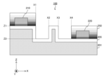
- FIG. 1 is a cross-sectional view showing one configuration example of a semiconductor device 100 according to a first embodiment of the present technology.
- This semiconductor device 100 includes a silicon substrate 201 and a mounting substrate 130 on which the silicon substrate 201 is mounted.
- an electronic device digital camera, smartphone, etc.
- the silicon substrate 201 is an example of the substrate described in the claims.
- X-axis a predetermined axis parallel to the substrate plane of the silicon substrate 201
- Z-axis an axis perpendicular to the substrate plane
- Y-axis An axis perpendicular to the X-axis and the Z-axis is defined as the "Y-axis”.
- This figure is a cross-sectional view seen from the Y-axis direction.
- the direction from the silicon substrate 201 to the mounting substrate 130 is referred to as the "upper" direction.
- a predetermined circuit (for example, a circuit that functions as a solid-state imaging device) is formed on the silicon substrate 201 .
- a predetermined number of wirings such as rewirings 210 and 220 are patterned on the upper surface of the silicon substrate 201 .
- a predetermined number of solder balls 121 are provided on the upper surface of the silicon substrate 201 . These solder balls 121 electrically connect the silicon substrate 201 to the mounting substrate 130 .
- Solder balls 121 contain, for example, tin.
- an underfill 110 is injected between the silicon substrate 201 and the mounting substrate 130 to seal the rewiring of the silicon substrate 201 and the like.
- the upper surface of the silicon substrate 201 is covered with an insulating film 205 such as a silicon oxynitride film (SiON film).
- the rewirings 210 and 220 are pulled out to the upper surface by TSV (Through Silicon Via) or the like and wired on the insulating film 205 .
- Each rewiring such as the rewiring 210 includes a wiring metal 212 and a barrier metal 211 for preventing diffusion of the wiring metal 212 into the insulating film 205 .
- the insulating film 205 is an example of the first insulating film described in the claims.
- the wiring metal 212 is, for example, one of Al (aluminum), Ag (silver), Au (gold) and Cu (copper), or an alloy of two or more of them. That is, the wiring metal 212 contains one or more of Al, Ag, Au and Cu. For example, a Cu wiring containing Cu as a main component is used as the rewiring.
- the barrier metal 211 contains, for example, any one of Ta (tantalum), TaN (tantalum nitride), Ti (titanium) and TiN (titanium nitride).
- each of the rewirings 210 and 220 is covered with a solder resist 250 .
- a gap 251 is provided between two adjacent wirings of the rewirings.
- the rewirings 210 and 220 are examples of the first wiring and the second wiring described in the claims.
- the rewirings 210 and 220 are wired in the Y-axis direction, and these wirings are assumed to be adjacent to each other.
- the solder resist 250 is not formed between the coordinate X1 on the right side of the rewiring 210 and the coordinate X2 on the left side of the rewiring 220 in the X-axis direction, and the insulating film 205 is exposed.
- Z1 is the coordinate of the upper surface of the solder resist 250 and Z2 is the coordinate of the upper surface of the insulating film 205
- (X1, Z1), (X1, Z2), (X2, Z1) and (X2, Z2) ) corresponds to the cross section of the gap 251 .
- the void 251 can also be expressed as a "groove” or a "gap".
- FIG. 2 is an example of a top view of the silicon substrate 201 before being coated with the solder resist 250 according to the first embodiment of the present technology.
- a predetermined number of solder balls 121 and a predetermined number of TSVs 122 are formed on the upper surface of the silicon substrate 201 .
- Rewirings 210 and 220 are wired on the insulating film 205, and the solder balls 121 and the TSVs 122 are connected by these wirings.
- rewirings 210 and 220 are laid adjacent to each other along the Y-axis direction.
- FIG. 3 is an example of a top view of the silicon substrate 201 after being coated with the solder resist 250 according to the first embodiment of the present technology.
- the rewirings 210 and 220 and the TSV 122 are covered with the solder resist 250 on this upper surface.
- the dashed-dotted line indicates the rewiring and the outline of the TSV 122 .
- a gap 251 is formed between two adjacent rewirings such as the rewirings 210 and 220 .
- a gap 251 is also formed between two adjacent TSVs 122 .
- the white portions correspond to the voids 251 .
- the underfill 110 in order to prevent the underfill 110 from entering between the gaps 251 , when injecting the underfill 110 , it is preferable to inject from the direction perpendicular to the wiring direction of the rewiring on both sides of the gap 251 .
- the underfill 110 can be injected from the X-axis direction.
- the arrow indicates the direction of injecting the underfill 110 .
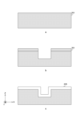
- FIG. 4 is a diagram for explaining manufacturing steps up to electrolytic plating in the first embodiment of the present technology.
- the upper surface of the silicon substrate 201 is flat, as illustrated by a in the figure.
- the manufacturing system deposits an insulating film 205 on the top surface, as illustrated in b in FIG. Then, the manufacturing system coats the barrier metal 211, arranges a photoresist 300 for forming a rewiring pattern, and electroplats the wiring metal 212 (such as Cu), as illustrated in c in FIG. I do.
- FIG. 5 is a diagram for explaining the manufacturing process up to coating with the solder resist 250 according to the first embodiment of the present technology.
- the manufacturing system removes, by etching, the barrier metal 211 and the wiring metal 212 at locations other than the wiring pattern from the silicon substrate 201 immediately after electroplating illustrated in a in the figure.
- rewirings 210 and 220 are formed as illustrated in b in FIG.
- the manufacturing system provides a gap between adjacent rewirings and covers the rewirings 210 and 220 with a solder resist 250, as illustrated in c in FIG.
- FIG. 6 is a flow chart showing an example of a manufacturing method according to the first embodiment of the present technology.
- the manufacturing system forms the insulating film 205 on the upper surface of the silicon substrate 201 (step S901) and performs electrolytic plating (step S902).
- step S903 the manufacturing system performs etching (step S903) and covers the rewiring with the solder resist 250 (step S904). Subsequently, the manufacturing system connects the silicon substrate 201 to the mounting board 130 with the solder balls 121 (step S905), and injects the underfill 110 (step S906). After step S ⁇ b>906 , the manufacturing system executes various processes as necessary, and completes the manufacturing process of the semiconductor device 100 .
- the space 251 is provided between the rewirings 210 and 220 and covered with the solder resist 250, ion migration can be prevented.
- the upper surfaces of the silicon substrate 201 and the insulating film 205 are flat, but in this configuration, ions may move on the insulating film 205 to cause ion migration.
- the semiconductor device 100 of the second embodiment differs from the first embodiment in that grooves are formed between adjacent wirings on the upper surfaces of the silicon substrate 201 and the insulating film 205 .
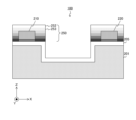
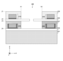
- FIG. 7 is a cross-sectional view showing one configuration example of the semiconductor device 100 according to the second embodiment of the present technology.
- the semiconductor device 100 of the second embodiment differs from the first embodiment in that grooves are formed in the silicon substrate 201 and the insulating film 205 between adjacent rewirings.
- the solder resist 250 is not formed and the insulating film 205 is exposed between the coordinate X1 on the right side of the rewiring 210 and the coordinate X2 on the left side of the rewiring 220 in the X-axis direction.
- the coordinate of the upper surface of the solder resist 250 is Z1
- the coordinate of the lower surface of the solder resist 250 (that is, the upper surface of the insulating film 205) is Z2.
- Z3 be the coordinate of the lower surface of the insulating film 205 immediately below the rewiring
- Z4 be the coordinate of the lower surface of the insulating film 205 below Z3.
- a U-shaped upside down shape passing through (X1, Z2), (X1, Z4), (X2, Z2) and (X2, Z4) corresponds to the cross section of the groove.
- grooves are formed in the same manner as in the insulating film 205. As shown in FIG.
- the position of the side surface of the solder resist 250 and the position of the side surface of the trench of the insulating film 205 are aligned (in other words, they are flush), but they should not be flush. can also
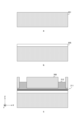
- FIG. 8 is a diagram for explaining the manufacturing process up to the formation of the insulating film 205 according to the second embodiment of the present technology.
- the upper surface of the silicon substrate 201 is flat in the initial state.
- the manufacturing system places a photoresist 301 for forming a groove pattern on the upper surface, and performs photolithography and dry etching, as illustrated in b in FIG. Then, the manufacturing system removes the photoresist 301 and deposits an insulating film 205, as illustrated in c in FIG.
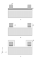
- FIG. 9 is a diagram for explaining a manufacturing process up to coating with a solder resist according to the second embodiment of the present technology.
- the manufacturing system coats a barrier metal 211, arranges a photoresist 302 for forming a rewiring pattern, and performs electroplating of the wiring metal 212, as exemplified by a in FIG.
- the manufacturing system removes the barrier metal 211 and the wiring metal 212 at locations other than the wiring pattern by etching, as illustrated in b in the figure.
- the manufacturing system provides a gap between adjacent rewirings and covers the rewirings 210 and 220 with a solder resist 250, as illustrated in c in FIG.
- c illustrates a case where the side surface of the solder resist 250 and the side surface of the insulating film 205 are not flush with each other.
- the trench is formed between the rewirings in the silicon substrate 201 and the insulating film 205 , it is possible to suppress the movement of ions on the insulating film 205 . can be done.
- the solder resist 250 is a single layer, but in this configuration, the effect of preventing ion diffusion and the effect of suppressing stress when the wiring metal 212 expands due to heat may be insufficient. be.
- the semiconductor device 100 according to the third embodiment differs from the second embodiment in that the solder resist 250 has multiple layers.
- FIG. 10 is a cross-sectional view showing one configuration example of the semiconductor device 100 according to the third embodiment of the present technology.
- Semiconductor device 100 of the third embodiment differs from the second embodiment in that solder resist 250 includes a plurality of layers such as upper layer 252 and middle layer 253 . These layers are stacked in the Z-axis direction. The density of each of these layers is assumed to be higher as it approaches the insulating film 205 . In the figure, the color depth of the layers in the solder resist 250 indicates the density.
- the third embodiment can be applied to the first embodiment without grooves.
- the solder resist 250 is formed in multiple layers, the effect of preventing ion diffusion and the effect of suppressing stress when the wiring metal 212 expands due to heat can be improved. can be done.
- the top surfaces of the silicon substrate 201 and the insulating film 205 are flat, but in this configuration, the effect of preventing ion migration may be insufficient.
- the semiconductor device 100 according to the fourth embodiment differs from the first embodiment in that the silicon substrate 201 and the insulating film 205 are stepped.
- FIG. 11 is a cross-sectional view showing one configuration example of the semiconductor device 100 according to the fourth embodiment of the present technology.
- the semiconductor device 100 of the fourth embodiment differs from the first embodiment in that a step is provided on the silicon substrate 201 and the insulating film 205 .
- the Z coordinate of the upper surface of the insulating film 205 is Z1 on the left side of X1, but Z2 on the right side of X1.
- the insulating film 205 has two planes with steps.
- the upper surface of the insulating film 205 on the left side of X1 in the figure is an example of the first plane described in the claims.
- the top surface of the insulating film 205 on the right side of X1 is an example of the second plane described in the claims.
- the upper surface of the silicon substrate 201 is also provided with a step in the same manner as the insulating film 205 .
- the rewiring 210 is wired on one of the two planes with the step, and the rewiring 220 is wired on the other of those planes.
- the rewirings 210 and 220 have different heights from a predetermined plane. By changing the height of the adjacent rewirings 210 and 220, the electric field between them can be weakened and the effect of preventing ion migration can be improved. Also, by changing the height, the distance between the rewirings can be increased to prevent short circuits due to ion migration.
- the insulating film 205 is provided with a step, the heights of the rewirings 210 and 220 can be changed. Thereby, the effect of preventing ion migration can be improved.
- the upper surfaces of the silicon substrate 201 and the insulating film 205 are flat, but in this configuration, ions may move on the insulating film 205 to cause ion migration.
- the semiconductor device 100 of the fifth embodiment differs from the first embodiment in that a plurality of grooves are formed between adjacent wirings on the upper surfaces of the silicon substrate 201 and the insulating film 205 .
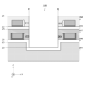
- FIG. 12 is a cross-sectional view showing one configuration example of the semiconductor device 100 according to the fifth embodiment of the present technology.
- the semiconductor device 100 of this fifth embodiment differs from the first embodiment in that two grooves are formed between the rewirings 210 and 220 in the silicon substrate 201 and the insulating film 205 .
- the first groove is formed from coordinates X1 to X2
- the second groove is formed from coordinates X3 to X4.
- the number of grooves between wirings is not limited to two, and may be three or more. By providing two or more grooves, it is possible to extend the movement distance of ions compared to the case of one groove, and to suppress the ions from reaching one of the rewirings 210 and 220 .
- the upper surfaces of the silicon substrate 201 and the insulating film 205 are flat, but in this configuration, the effect of preventing ion migration may be insufficient.
- the semiconductor device 100 according to the sixth embodiment differs from the first embodiment in that steps are provided in the silicon substrate 201 and the insulating film 205, and a protrusion is provided between the rewirings.
- FIG. 13 is a cross-sectional view showing one configuration example of the semiconductor device 100 according to the sixth embodiment of the present technology.
- the semiconductor device 100 of the sixth embodiment is different from the first embodiment in that a step is provided in the silicon substrate 201 and the insulating film 205, and a protrusion is provided between the rewirings 210 and 220. Different from the form.
- the semiconductor device 100 of the sixth embodiment differs from the first embodiment in that the solder resist 250 is multi-layered.
- the Z coordinate of the upper surface of the insulating film 205 is Z1 on the left side of X1, but Z2 on the right side of X1.
- a protrusion projecting from the XY plane of the coordinate Z1 is provided to the coordinates X2 to X3.
- solder resist 250 is multi-layered, it may be a single layer.
- the insulating film 205 is provided with a step and the protrusion is formed between the rewirings, the movement of ions on the insulating film 205 can be suppressed. can be done.
- the layers of the rewirings 210 and 220 are single layers, but in this configuration, the wiring density may be insufficient.
- the semiconductor device 100 according to the sixth embodiment differs from the first embodiment in that the rewiring layers are multi-layered.
- FIG. 14 is a cross-sectional view showing one configuration example of the semiconductor device 100 according to the seventh embodiment of the present technology.
- the semiconductor device 100 of the seventh embodiment differs from the first embodiment in that the number of rewiring layers is two.
- the lower redistribution layer includes redistribution lines 230 and 240 , which are routed on top of the insulating film 206 and covered by the insulating layer 207 .
- As a material for the insulating layer 207 SiO, SiN, SiON, or the like is used.
- the barrier metal is also formed on the side surfaces of the wirings.
- An air gap is provided between the redistribution lines 210 and 220 in the lower insulating layer 207 . This void is referred to as the "lower layer space".
- the insulating layer 207 and the upper surface of the lower layer space are covered with the insulating film 205 .
- the lower layer space is formed by wet etching or the like to form a hollow structure, a portion of the insulating film 205 is removed by dry or wet etching to form a hole.
- the insulating film 206 is an example of the second insulating film described in the claims.
- the upper rewiring layer includes rewirings 210 and 220 , which are wired on the top surface of the insulating film 205 and covered with a solder resist 250 .
- a gap is provided between the rewirings 210 and 220 in the upper solder resist 250 . This void is referred to as the "upper space”.
- the rewirings 230 and 240 are examples of the third wiring and the fourth wiring described in the claims.
- Z1 be the Z coordinate of the upper surface of the solder resist 250
- Z2 be the Z coordinate of its lower surface
- the Z coordinate of the top surface of the insulating layer 207 is Z3, and the Z coordinate of the bottom surface thereof is Z4.
- a rectangle with vertices at (X1, Z3), (X1, Z4), (X2, Z3) and (X2, Z4) is the cross section of the lower space. Applicable.
- the rectangles having vertices (X1, Z1), (X1, Z2), (X2, Z1) and (X2, Z2) correspond to cross sections of the upper space.
- each of the second, third, fourth, fifth and sixth embodiments can be applied to the seventh embodiment.
- the wiring density can be increased.
- FIG. 15 is a cross-sectional view showing one configuration example of the semiconductor device 100 according to the eighth embodiment of the present technology.
- the semiconductor device 100 of the eighth embodiment is similar to the seventh embodiment in that the insulating film 205 is removed from the gap between the wirings and grooves are formed in the lower insulating film 206 and the silicon substrate 201 . different from By removing the insulating film 205 from the gap between the wirings, the need for a hollow structure is eliminated.
- Z5 be the Z coordinate of the lower surface of the insulating film 206 immediately below the insulating layer 207
- Z6 be the coordinate of the lower surface of the insulating film 206 below Z5.
- the U-shape passing through (X1, Z4), (X1, Z6), (X2, Z4) and (X2, Z6) corresponds to the section of the groove.
- the insulating film 205 is removed from the gaps between the wirings, there is no need for a hollow structure.
- the groove is formed between the rewirings in the silicon substrate 201 and the insulating film 206 , the movement of ions on the insulating film 206 can be suppressed.
- the technology (the present technology) according to the present disclosure can be applied to various products.
- the technology according to the present disclosure can be realized as a device mounted on any type of moving body such as automobiles, electric vehicles, hybrid electric vehicles, motorcycles, bicycles, personal mobility, airplanes, drones, ships, and robots. may
- FIG. 16 is a block diagram showing a schematic configuration example of a vehicle control system, which is an example of a mobile control system to which the technology according to the present disclosure can be applied.
- a vehicle control system 12000 includes a plurality of electronic control units connected via a communication network 12001.
- the vehicle control system 12000 includes a drive train control unit 12010, a body system control unit 12020, an outside information detection unit 12030, an inside information detection unit 12040, and an integrated control unit 12050.
- a microcomputer 12051, an audio/image output unit 12052, and an in-vehicle network I/F (interface) 12053 are illustrated.
- the drive system control unit 12010 controls the operation of devices related to the drive system of the vehicle according to various programs.
- the driving system control unit 12010 includes a driving force generator for generating driving force of the vehicle such as an internal combustion engine or a driving motor, a driving force transmission mechanism for transmitting the driving force to the wheels, and a steering angle of the vehicle. It functions as a control device such as a steering mechanism to adjust and a brake device to generate braking force of the vehicle.
- the body system control unit 12020 controls the operation of various devices equipped on the vehicle body according to various programs.
- the body system control unit 12020 functions as a keyless entry system, a smart key system, a power window device, or a control device for various lamps such as headlamps, back lamps, brake lamps, winkers or fog lamps.
- body system control unit 12020 can receive radio waves transmitted from a portable device that substitutes for a key or signals from various switches.
- the body system control unit 12020 receives the input of these radio waves or signals and controls the door lock device, power window device, lamps, etc. of the vehicle.
- the vehicle exterior information detection unit 12030 detects information outside the vehicle in which the vehicle control system 12000 is installed.
- the vehicle exterior information detection unit 12030 is connected with an imaging section 12031 .
- the vehicle exterior information detection unit 12030 causes the imaging unit 12031 to capture an image of the exterior of the vehicle, and receives the captured image.
- the vehicle exterior information detection unit 12030 may perform object detection processing or distance detection processing such as people, vehicles, obstacles, signs, or characters on the road surface based on the received image.
- the imaging unit 12031 is an optical sensor that receives light and outputs an electrical signal according to the amount of received light.
- the imaging unit 12031 can output the electric signal as an image, and can also output it as distance measurement information.
- the light received by the imaging unit 12031 may be visible light or non-visible light such as infrared rays.
- the in-vehicle information detection unit 12040 detects in-vehicle information.
- the in-vehicle information detection unit 12040 is connected to, for example, a driver state detection section 12041 that detects the state of the driver.
- the driver state detection unit 12041 includes, for example, a camera that captures an image of the driver, and the in-vehicle information detection unit 12040 detects the degree of fatigue or concentration of the driver based on the detection information input from the driver state detection unit 12041. It may be calculated, or it may be determined whether the driver is dozing off.
- the microcomputer 12051 calculates control target values for the driving force generator, the steering mechanism, or the braking device based on the information inside and outside the vehicle acquired by the vehicle exterior information detection unit 12030 or the vehicle interior information detection unit 12040, and controls the drive system control unit.
- a control command can be output to 12010 .
- the microcomputer 12051 realizes the functions of ADAS (Advanced Driver Assistance System) including collision avoidance or shock mitigation, follow-up driving based on inter-vehicle distance, vehicle speed maintenance driving, vehicle collision warning, or vehicle lane deviation warning. Cooperative control can be performed for the purpose of ADAS (Advanced Driver Assistance System) including collision avoidance or shock mitigation, follow-up driving based on inter-vehicle distance, vehicle speed maintenance driving, vehicle collision warning, or vehicle lane deviation warning. Cooperative control can be performed for the purpose of ADAS (Advanced Driver Assistance System) including collision avoidance or shock mitigation, follow-up driving based on inter-vehicle distance, vehicle speed maintenance driving, vehicle collision warning, or vehicle
- the microcomputer 12051 controls the driving force generator, the steering mechanism, the braking device, etc. based on the information about the vehicle surroundings acquired by the vehicle exterior information detection unit 12030 or the vehicle interior information detection unit 12040, so that the driver's Cooperative control can be performed for the purpose of autonomous driving, etc., in which vehicles autonomously travel without depending on operation.
- the microcomputer 12051 can output a control command to the body system control unit 12020 based on the information outside the vehicle acquired by the information detection unit 12030 outside the vehicle.
- the microcomputer 12051 controls the headlamps according to the position of the preceding vehicle or the oncoming vehicle detected by the vehicle exterior information detection unit 12030, and performs cooperative control aimed at anti-glare such as switching from high beam to low beam. It can be carried out.
- the audio/image output unit 12052 transmits at least one of audio and/or image output signals to an output device capable of visually or audibly notifying the passengers of the vehicle or the outside of the vehicle.
- an audio speaker 12061, a display unit 12062, and an instrument panel 12063 are illustrated as output devices.
- the display unit 12062 may include at least one of an on-board display and a head-up display, for example.
- FIG. 17 is a diagram showing an example of the installation position of the imaging unit 12031.
- the imaging unit 12031 has imaging units 12101, 12102, 12103, 12104, and 12105.
- the imaging units 12101, 12102, 12103, 12104, and 12105 are provided at positions such as the front nose of the vehicle 12100, the side mirrors, the rear bumper, the back door, and the upper part of the windshield in the vehicle interior, for example.
- An image pickup unit 12101 provided in the front nose and an image pickup unit 12105 provided above the windshield in the passenger compartment mainly acquire images in front of the vehicle 12100 .
- Imaging units 12102 and 12103 provided in the side mirrors mainly acquire side images of the vehicle 12100 .
- An imaging unit 12104 provided in the rear bumper or back door mainly acquires an image behind the vehicle 12100 .
- the imaging unit 12105 provided above the windshield in the passenger compartment is mainly used for detecting preceding vehicles, pedestrians, obstacles, traffic lights, traffic signs, lanes, and the like.
- FIG. 17 shows an example of the imaging range of the imaging units 12101 to 12104.
- the imaging range 12111 indicates the imaging range of the imaging unit 12101 provided in the front nose
- the imaging ranges 12112 and 12113 indicate the imaging ranges of the imaging units 12102 and 12103 provided in the side mirrors, respectively
- the imaging range 12114 The imaging range of an imaging unit 12104 provided in the rear bumper or back door is shown. For example, by superimposing the image data captured by the imaging units 12101 to 12104, a bird's-eye view image of the vehicle 12100 viewed from above can be obtained.
- At least one of the imaging units 12101 to 12104 may have a function of acquiring distance information.
- at least one of the imaging units 12101 to 12104 may be a stereo camera composed of a plurality of imaging elements, or may be an imaging element having pixels for phase difference detection.
- the microcomputer 12051 determines the distance to each three-dimensional object within the imaging ranges 12111 to 12114 and changes in this distance over time (relative velocity with respect to the vehicle 12100). , it is possible to extract, as the preceding vehicle, the closest three-dimensional object on the course of the vehicle 12100, which runs at a predetermined speed (for example, 0 km/h or more) in substantially the same direction as the vehicle 12100. can. Furthermore, the microcomputer 12051 can set the inter-vehicle distance to be secured in advance in front of the preceding vehicle, and perform automatic brake control (including following stop control) and automatic acceleration control (including following start control). In this way, cooperative control can be performed for the purpose of automatic driving in which the vehicle runs autonomously without relying on the operation of the driver.
- automatic brake control including following stop control
- automatic acceleration control including following start control
- the microcomputer 12051 converts three-dimensional object data related to three-dimensional objects to other three-dimensional objects such as motorcycles, ordinary vehicles, large vehicles, pedestrians, and utility poles. It can be classified and extracted and used for automatic avoidance of obstacles. For example, the microcomputer 12051 distinguishes obstacles around the vehicle 12100 into those that are visible to the driver of the vehicle 12100 and those that are difficult to see. Then, the microcomputer 12051 judges the collision risk indicating the degree of danger of collision with each obstacle, and when the collision risk is equal to or higher than the set value and there is a possibility of collision, an audio speaker 12061 and a display unit 12062 are displayed. By outputting an alarm to the driver via the drive system control unit 12010 and performing forced deceleration and avoidance steering via the drive system control unit 12010, driving support for collision avoidance can be performed.
- At least one of the imaging units 12101 to 12104 may be an infrared camera that detects infrared rays.
- the microcomputer 12051 can recognize a pedestrian by determining whether or not the pedestrian exists in the captured images of the imaging units 12101 to 12104 .
- recognition of a pedestrian is performed by, for example, a procedure for extracting feature points in images captured by the imaging units 12101 to 12104 as infrared cameras, and performing pattern matching processing on a series of feature points indicating the outline of an object to determine whether or not the pedestrian is a pedestrian.
- the audio image output unit 12052 outputs a rectangular outline for emphasis to the recognized pedestrian. is superimposed on the display unit 12062 . Also, the audio/image output unit 12052 may control the display unit 12062 to display an icon or the like indicating a pedestrian at a desired position.
- the technology according to the present disclosure can be applied to, for example, the imaging unit 12031 among the configurations described above.
- the semiconductor device 100 in FIG. 1 can be applied to the imaging portion 12031 .
- Example of application to an endoscopic surgery system The technology (the present technology) according to the present disclosure can be applied to various products.
- the technology according to the present disclosure may be applied to an endoscopic surgery system.
- FIG. 18 is a diagram showing an example of a schematic configuration of an endoscopic surgery system to which the technology (this technology) according to the present disclosure can be applied.
- FIG. 18 shows a state in which an operator (doctor) 11131 is performing surgery on a patient 11132 on a patient bed 11133 using an endoscopic surgery system 11000 .
- an endoscopic surgery system 11000 includes an endoscope 11100, other surgical instruments 11110 such as a pneumoperitoneum tube 11111 and an energy treatment instrument 11112, and a support arm device 11120 for supporting the endoscope 11100. , and a cart 11200 loaded with various devices for endoscopic surgery.
- An endoscope 11100 is composed of a lens barrel 11101 whose distal end is inserted into the body cavity of a patient 11132 and a camera head 11102 connected to the proximal end of the lens barrel 11101 .
- an endoscope 11100 configured as a so-called rigid scope having a rigid lens barrel 11101 is illustrated, but the endoscope 11100 may be configured as a so-called flexible scope having a flexible lens barrel. good.
- the tip of the lens barrel 11101 is provided with an opening into which the objective lens is fitted.
- a light source device 11203 is connected to the endoscope 11100, and light generated by the light source device 11203 is guided to the tip of the lens barrel 11101 by a light guide extending inside the lens barrel 11101, where it reaches the objective. Through the lens, the light is irradiated toward the observation object inside the body cavity of the patient 11132 .
- the endoscope 11100 may be a straight scope, a perspective scope, or a side scope.
- An optical system and an imaging element are provided inside the camera head 11102, and the reflected light (observation light) from the observation target is focused on the imaging element by the optical system.
- the imaging device photoelectrically converts the observation light to generate an electrical signal corresponding to the observation light, that is, an image signal corresponding to the observation image.
- the image signal is transmitted to a camera control unit (CCU: Camera Control Unit) 11201 as RAW data.
- CCU Camera Control Unit
- the CCU 11201 is composed of a CPU (Central Processing Unit), a GPU (Graphics Processing Unit), etc., and controls the operations of the endoscope 11100 and the display device 11202 in an integrated manner. Further, the CCU 11201 receives an image signal from the camera head 11102 and performs various image processing such as development processing (demosaicing) for displaying an image based on the image signal.
- CPU Central Processing Unit
- GPU Graphics Processing Unit
- the display device 11202 displays an image based on an image signal subjected to image processing by the CCU 11201 under the control of the CCU 11201 .
- the light source device 11203 is composed of a light source such as an LED (light emitting diode), for example, and supplies the endoscope 11100 with irradiation light for imaging a surgical site or the like.
- a light source such as an LED (light emitting diode)
- LED light emitting diode
- the input device 11204 is an input interface for the endoscopic surgery system 11000.
- the user can input various information and instructions to the endoscopic surgery system 11000 via the input device 11204 .
- the user inputs an instruction or the like to change the imaging conditions (type of irradiation light, magnification, focal length, etc.) by the endoscope 11100 .
- the treatment instrument control device 11205 controls driving of the energy treatment instrument 11112 for tissue cauterization, incision, blood vessel sealing, or the like.
- the pneumoperitoneum device 11206 inflates the body cavity of the patient 11132 for the purpose of securing the visual field of the endoscope 11100 and securing the operator's working space, and injects gas into the body cavity through the pneumoperitoneum tube 11111. send in.
- the recorder 11207 is a device capable of recording various types of information regarding surgery.
- the printer 11208 is a device capable of printing various types of information regarding surgery in various formats such as text, images, and graphs.
- the light source device 11203 that supplies the endoscope 11100 with irradiation light for photographing the surgical site can be composed of, for example, a white light source composed of an LED, a laser light source, or a combination thereof.
- a white light source is configured by a combination of RGB laser light sources
- the output intensity and output timing of each color (each wavelength) can be controlled with high accuracy. It can be carried out.
- the observation target is irradiated with laser light from each of the RGB laser light sources in a time division manner, and by controlling the drive of the imaging device of the camera head 11102 in synchronization with the irradiation timing, each of RGB can be handled. It is also possible to pick up images by time division. According to this method, a color image can be obtained without providing a color filter in the imaging element.
- the driving of the light source device 11203 may be controlled so as to change the intensity of the output light every predetermined time.
- the drive of the imaging device of the camera head 11102 in synchronism with the timing of the change in the intensity of the light to obtain an image in a time-division manner and synthesizing the images, a high dynamic A range of images can be generated.
- the light source device 11203 may be configured to be able to supply light in a predetermined wavelength band corresponding to special light observation.
- special light observation for example, by utilizing the wavelength dependence of light absorption in body tissues, by irradiating light with a narrower band than the irradiation light (i.e., white light) during normal observation, the mucosal surface layer So-called Narrow Band Imaging, in which a predetermined tissue such as a blood vessel is imaged with high contrast, is performed.
- fluorescence observation may be performed in which an image is obtained from fluorescence generated by irradiation with excitation light.
- the body tissue is irradiated with excitation light and the fluorescence from the body tissue is observed (autofluorescence observation), or a reagent such as indocyanine green (ICG) is locally injected into the body tissue and the body tissue is examined.
- a fluorescence image can be obtained by irradiating excitation light corresponding to the fluorescence wavelength of the reagent.
- the light source device 11203 can be configured to be able to supply narrowband light and/or excitation light corresponding to such special light observation.
- FIG. 19 is a block diagram showing an example of functional configurations of the camera head 11102 and CCU 11201 shown in FIG.
- the camera head 11102 has a lens unit 11401, an imaging section 11402, a drive section 11403, a communication section 11404, and a camera head control section 11405.
- the CCU 11201 has a communication section 11411 , an image processing section 11412 and a control section 11413 .
- the camera head 11102 and the CCU 11201 are communicably connected to each other via a transmission cable 11400 .
- a lens unit 11401 is an optical system provided at a connection with the lens barrel 11101 . Observation light captured from the tip of the lens barrel 11101 is guided to the camera head 11102 and enters the lens unit 11401 .
- a lens unit 11401 is configured by combining a plurality of lenses including a zoom lens and a focus lens.
- the number of imaging elements constituting the imaging unit 11402 may be one (so-called single-plate type) or plural (so-called multi-plate type).
- image signals corresponding to RGB may be generated by each image pickup element, and a color image may be obtained by synthesizing the image signals.
- the imaging unit 11402 may be configured to have a pair of imaging elements for respectively acquiring right-eye and left-eye image signals corresponding to 3D (dimensional) display.
- the 3D display enables the operator 11131 to more accurately grasp the depth of the living tissue in the surgical site.
- a plurality of systems of lens units 11401 may be provided corresponding to each imaging element.
- the imaging unit 11402 does not necessarily have to be provided in the camera head 11102 .
- the imaging unit 11402 may be provided inside the lens barrel 11101 immediately after the objective lens.
- the drive unit 11403 is configured by an actuator, and moves the zoom lens and focus lens of the lens unit 11401 by a predetermined distance along the optical axis under control from the camera head control unit 11405 . Thereby, the magnification and focus of the image captured by the imaging unit 11402 can be appropriately adjusted.
- the communication unit 11404 is composed of a communication device for transmitting and receiving various information to and from the CCU 11201.
- the communication unit 11404 transmits the image signal obtained from the imaging unit 11402 as RAW data to the CCU 11201 via the transmission cable 11400 .
- the communication unit 11404 receives a control signal for controlling driving of the camera head 11102 from the CCU 11201 and supplies it to the camera head control unit 11405 .
- the control signal includes, for example, information to specify the frame rate of the captured image, information to specify the exposure value at the time of imaging, and/or information to specify the magnification and focus of the captured image. Contains information about conditions.
- the imaging conditions such as the frame rate, exposure value, magnification, and focus may be appropriately designated by the user, or may be automatically set by the control unit 11413 of the CCU 11201 based on the acquired image signal. good.
- the endoscope 11100 is equipped with so-called AE (Auto Exposure) function, AF (Auto Focus) function, and AWB (Auto White Balance) function.
- the camera head control unit 11405 controls driving of the camera head 11102 based on the control signal from the CCU 11201 received via the communication unit 11404.
- the communication unit 11411 is composed of a communication device for transmitting and receiving various information to and from the camera head 11102 .
- the communication unit 11411 receives image signals transmitted from the camera head 11102 via the transmission cable 11400 .
- the communication unit 11411 transmits a control signal for controlling driving of the camera head 11102 to the camera head 11102 .
- Image signals and control signals can be transmitted by electrical communication, optical communication, or the like.
- the image processing unit 11412 performs various types of image processing on the image signal, which is RAW data transmitted from the camera head 11102 .
- the control unit 11413 performs various controls related to imaging of the surgical site and the like by the endoscope 11100 and display of the captured image obtained by imaging the surgical site and the like. For example, the control unit 11413 generates control signals for controlling driving of the camera head 11102 .
- control unit 11413 causes the display device 11202 to display a captured image showing the surgical site and the like based on the image signal that has undergone image processing by the image processing unit 11412 .
- the control unit 11413 may recognize various objects in the captured image using various image recognition techniques. For example, the control unit 11413 detects the shape, color, and the like of the edges of objects included in the captured image, thereby detecting surgical instruments such as forceps, specific body parts, bleeding, mist during use of the energy treatment instrument 11112, and the like. can recognize.
- the control unit 11413 may use the recognition result to display various types of surgical assistance information superimposed on the image of the surgical site. By superimposing and presenting the surgery support information to the operator 11131, the burden on the operator 11131 can be reduced and the operator 11131 can proceed with the surgery reliably.
- a transmission cable 11400 connecting the camera head 11102 and the CCU 11201 is an electrical signal cable compatible with electrical signal communication, an optical fiber compatible with optical communication, or a composite cable of these.
- wired communication is performed using the transmission cable 11400, but communication between the camera head 11102 and the CCU 11201 may be performed wirelessly.
- the technology according to the present disclosure can be applied to the imaging unit 11402 among the configurations described above.
- the semiconductor device 100 in FIG. 1 can be applied to the imaging portion 10402 .
- the technology according to the present disclosure may also be applied to, for example, a microsurgery system.
- the present technology can also have the following configuration.
- a semiconductor device comprising a solder resist covering the first wiring and the second wiring with a gap provided between the first wiring and the second wiring.
- the first insulating film has a stepped first plane and a second plane;
- the first wiring is wired on the first plane,
- the gap includes a lower layer space between the first wiring and the second wiring and an upper layer space between the third wiring and the fourth wiring;
- the gap is provided between the laminated first wiring and the third wiring and the laminated second wiring and the fourth wiring;
- the solder resist comprises a plurality of layers;
- each of the first wiring and the second wiring includes a wiring metal;
- the semiconductor device according to any one of (1) to (10), wherein the wiring metal includes at least one of aluminum, silver, gold and copper.
- each of the first wiring and the second wiring includes a barrier metal;
- the barrier metal includes any one of tantalum, tantalum nitride, titanium and titanium nitride.
- (13) further comprising a solder ball connected to at least one of the first wiring and the second wiring;
- (14) further comprising a first via and a second via;
- the semiconductor device according to any one of (1) to (13), wherein the solder resist further includes a space between the first via and the second via.
- a method of manufacturing a semiconductor device comprising: (16) The method of manufacturing a semiconductor device according to (15), further comprising an injection procedure of injecting underfill from a direction perpendicular to the wiring direction of the first wiring and the second wiring.
Landscapes
- Internal Circuitry In Semiconductor Integrated Circuit Devices (AREA)
Priority Applications (4)
| Application Number | Priority Date | Filing Date | Title |
|---|---|---|---|
| EP22920479.7A EP4468333A1 (en) | 2022-01-17 | 2022-11-29 | Semiconductor device and manufacturing method for semiconductor device |
| CN202280088366.1A CN118525367A (zh) | 2022-01-17 | 2022-11-29 | 半导体设备和用于制造半导体设备的方法 |
| US18/727,179 US20250081657A1 (en) | 2022-01-17 | 2022-11-29 | Semiconductor device and method for manufacturing semiconductor device |
| JP2023573890A JPWO2023135959A1 (https=) | 2022-01-17 | 2022-11-29 |
Applications Claiming Priority (2)
| Application Number | Priority Date | Filing Date | Title |
|---|---|---|---|
| JP2022004775 | 2022-01-17 | ||
| JP2022-004775 | 2022-01-17 |
Publications (1)
| Publication Number | Publication Date |
|---|---|
| WO2023135959A1 true WO2023135959A1 (ja) | 2023-07-20 |
Family
ID=87278787
Family Applications (1)
| Application Number | Title | Priority Date | Filing Date |
|---|---|---|---|
| PCT/JP2022/043889 Ceased WO2023135959A1 (ja) | 2022-01-17 | 2022-11-29 | 半導体装置、および、半導体装置の製造方法 |
Country Status (5)
| Country | Link |
|---|---|
| US (1) | US20250081657A1 (https=) |
| EP (1) | EP4468333A1 (https=) |
| JP (1) | JPWO2023135959A1 (https=) |
| CN (1) | CN118525367A (https=) |
| WO (1) | WO2023135959A1 (https=) |
Citations (6)
| Publication number | Priority date | Publication date | Assignee | Title |
|---|---|---|---|---|
| JP2003332483A (ja) * | 2002-05-16 | 2003-11-21 | Hitachi Ltd | 配線基板とそれを用いた電子装置 |
| JP2005093652A (ja) * | 2003-09-17 | 2005-04-07 | Casio Comput Co Ltd | 半導体装置 |
| JP2008034472A (ja) * | 2006-07-26 | 2008-02-14 | Sony Corp | 半導体装置及びその製造方法 |
| JP2009152317A (ja) * | 2007-12-19 | 2009-07-09 | Panasonic Corp | 半導体装置およびその製造方法 |
| JP2016051834A (ja) | 2014-09-01 | 2016-04-11 | イビデン株式会社 | プリント配線基板およびその製造方法 |
| JP2018093129A (ja) * | 2016-12-07 | 2018-06-14 | 日立オートモティブシステムズ株式会社 | 半導体装置 |
-
2022
- 2022-11-29 US US18/727,179 patent/US20250081657A1/en active Pending
- 2022-11-29 JP JP2023573890A patent/JPWO2023135959A1/ja active Pending
- 2022-11-29 CN CN202280088366.1A patent/CN118525367A/zh not_active Withdrawn
- 2022-11-29 WO PCT/JP2022/043889 patent/WO2023135959A1/ja not_active Ceased
- 2022-11-29 EP EP22920479.7A patent/EP4468333A1/en not_active Withdrawn
Patent Citations (6)
| Publication number | Priority date | Publication date | Assignee | Title |
|---|---|---|---|---|
| JP2003332483A (ja) * | 2002-05-16 | 2003-11-21 | Hitachi Ltd | 配線基板とそれを用いた電子装置 |
| JP2005093652A (ja) * | 2003-09-17 | 2005-04-07 | Casio Comput Co Ltd | 半導体装置 |
| JP2008034472A (ja) * | 2006-07-26 | 2008-02-14 | Sony Corp | 半導体装置及びその製造方法 |
| JP2009152317A (ja) * | 2007-12-19 | 2009-07-09 | Panasonic Corp | 半導体装置およびその製造方法 |
| JP2016051834A (ja) | 2014-09-01 | 2016-04-11 | イビデン株式会社 | プリント配線基板およびその製造方法 |
| JP2018093129A (ja) * | 2016-12-07 | 2018-06-14 | 日立オートモティブシステムズ株式会社 | 半導体装置 |
Also Published As
| Publication number | Publication date |
|---|---|
| CN118525367A (zh) | 2024-08-20 |
| US20250081657A1 (en) | 2025-03-06 |
| EP4468333A1 (en) | 2024-11-27 |
| JPWO2023135959A1 (https=) | 2023-07-20 |
Similar Documents
| Publication | Publication Date | Title |
|---|---|---|
| JP7037547B2 (ja) | 半導体装置、半導体装置の製造方法、及び電子機器 | |
| WO2019087764A1 (ja) | 裏面照射型の固体撮像装置、および裏面照射型の固体撮像装置の製造方法、撮像装置、並びに電子機器 | |
| US12211819B2 (en) | Method of manufacturing semiconductor device and semiconductor device | |
| JP6951866B2 (ja) | 撮像素子 | |
| JP7227235B2 (ja) | 撮像素子および撮像装置 | |
| WO2021193266A1 (ja) | 固体撮像装置 | |
| WO2020246323A1 (ja) | 撮像装置 | |
| JP2023164552A (ja) | 固体撮像装置及び電子機器 | |
| WO2019135333A1 (ja) | 半導体装置 | |
| WO2022244297A1 (ja) | 固体撮像装置及び電子機器 | |
| WO2019107002A1 (ja) | 半導体装置および半導体装置の製造方法 | |
| US20220005853A1 (en) | Semiconductor device, solid-state imaging device, and electronic equipment | |
| WO2023135959A1 (ja) | 半導体装置、および、半導体装置の製造方法 | |
| WO2021049302A1 (ja) | 撮像装置、電子機器、製造方法 | |
| TWI825178B (zh) | 攝像裝置 | |
| US20240096919A1 (en) | Semiconductor device, imaging device, and manufacturing method | |
| US20240297196A1 (en) | Semiconductor device and imaging device | |
| EP4307373A1 (en) | Semiconductor device and imaging device | |
| US20240055326A1 (en) | Semiconductor device and method for manufacturing semiconductor device | |
| JP7136800B2 (ja) | 半導体装置および半導体装置の製造方法、並びに撮像装置 | |
| WO2023021787A1 (ja) | 光検出装置およびその製造方法 | |
| WO2022123901A1 (ja) | 半導体装置、および、半導体装置の製造方法 |
Legal Events
| Date | Code | Title | Description |
|---|---|---|---|
| 121 | Ep: the epo has been informed by wipo that ep was designated in this application |
Ref document number: 22920479 Country of ref document: EP Kind code of ref document: A1 |
|
| ENP | Entry into the national phase |
Ref document number: 2023573890 Country of ref document: JP Kind code of ref document: A |
|
| WWE | Wipo information: entry into national phase |
Ref document number: 18727179 Country of ref document: US |
|
| WWE | Wipo information: entry into national phase |
Ref document number: 202280088366.1 Country of ref document: CN |
|
| WWE | Wipo information: entry into national phase |
Ref document number: 2022920479 Country of ref document: EP |
|
| NENP | Non-entry into the national phase |
Ref country code: DE |
|
| ENP | Entry into the national phase |
Ref document number: 2022920479 Country of ref document: EP Effective date: 20240819 |
|
| WWP | Wipo information: published in national office |
Ref document number: 18727179 Country of ref document: US |
|
| WWW | Wipo information: withdrawn in national office |
Ref document number: 2022920479 Country of ref document: EP |