WO2023132278A1 - コイル装置及びプリント配線板 - Google Patents
コイル装置及びプリント配線板 Download PDFInfo
- Publication number
- WO2023132278A1 WO2023132278A1 PCT/JP2022/047696 JP2022047696W WO2023132278A1 WO 2023132278 A1 WO2023132278 A1 WO 2023132278A1 JP 2022047696 W JP2022047696 W JP 2022047696W WO 2023132278 A1 WO2023132278 A1 WO 2023132278A1
- Authority
- WO
- WIPO (PCT)
- Prior art keywords
- coil
- main surface
- area
- wiring
- layer
- Prior art date
- Legal status (The legal status is an assumption and is not a legal conclusion. Google has not performed a legal analysis and makes no representation as to the accuracy of the status listed.)
- Ceased
Links
Images







Classifications
-
- H—ELECTRICITY
- H01—ELECTRIC ELEMENTS
- H01F—MAGNETS; INDUCTANCES; TRANSFORMERS; SELECTION OF MATERIALS FOR THEIR MAGNETIC PROPERTIES
- H01F17/00—Fixed inductances of the signal type
- H01F17/0006—Printed inductances
- H01F17/0013—Printed inductances with stacked layers
-
- H—ELECTRICITY
- H05—ELECTRIC TECHNIQUES NOT OTHERWISE PROVIDED FOR
- H05K—PRINTED CIRCUITS; CASINGS OR CONSTRUCTIONAL DETAILS OF ELECTRIC APPARATUS; MANUFACTURE OF ASSEMBLAGES OF ELECTRICAL COMPONENTS
- H05K3/00—Apparatus or processes for manufacturing printed circuits
- H05K3/38—Improvement of the adhesion between the insulating substrate and the metal
- H05K3/386—Improvement of the adhesion between the insulating substrate and the metal by the use of an organic polymeric bonding layer, e.g. adhesive
-
- H—ELECTRICITY
- H01—ELECTRIC ELEMENTS
- H01F—MAGNETS; INDUCTANCES; TRANSFORMERS; SELECTION OF MATERIALS FOR THEIR MAGNETIC PROPERTIES
- H01F17/00—Fixed inductances of the signal type
-
- H—ELECTRICITY
- H01—ELECTRIC ELEMENTS
- H01F—MAGNETS; INDUCTANCES; TRANSFORMERS; SELECTION OF MATERIALS FOR THEIR MAGNETIC PROPERTIES
- H01F17/00—Fixed inductances of the signal type
- H01F17/02—Fixed inductances of the signal type without magnetic core
-
- H—ELECTRICITY
- H01—ELECTRIC ELEMENTS
- H01F—MAGNETS; INDUCTANCES; TRANSFORMERS; SELECTION OF MATERIALS FOR THEIR MAGNETIC PROPERTIES
- H01F27/00—Details of transformers or inductances, in general
- H01F27/28—Coils; Windings; Conductive connections
-
- H—ELECTRICITY
- H01—ELECTRIC ELEMENTS
- H01F—MAGNETS; INDUCTANCES; TRANSFORMERS; SELECTION OF MATERIALS FOR THEIR MAGNETIC PROPERTIES
- H01F27/00—Details of transformers or inductances, in general
- H01F27/28—Coils; Windings; Conductive connections
- H01F27/2804—Printed windings
-
- H—ELECTRICITY
- H01—ELECTRIC ELEMENTS
- H01F—MAGNETS; INDUCTANCES; TRANSFORMERS; SELECTION OF MATERIALS FOR THEIR MAGNETIC PROPERTIES
- H01F27/00—Details of transformers or inductances, in general
- H01F27/28—Coils; Windings; Conductive connections
- H01F27/29—Terminals; Tapping arrangements for signal inductances
-
- H—ELECTRICITY
- H05—ELECTRIC TECHNIQUES NOT OTHERWISE PROVIDED FOR
- H05K—PRINTED CIRCUITS; CASINGS OR CONSTRUCTIONAL DETAILS OF ELECTRIC APPARATUS; MANUFACTURE OF ASSEMBLAGES OF ELECTRICAL COMPONENTS
- H05K1/00—Printed circuits
- H05K1/02—Details
- H05K1/11—Printed elements for providing electric connections to or between printed circuits
- H05K1/115—Via connections; Lands around holes or via connections
-
- H—ELECTRICITY
- H05—ELECTRIC TECHNIQUES NOT OTHERWISE PROVIDED FOR
- H05K—PRINTED CIRCUITS; CASINGS OR CONSTRUCTIONAL DETAILS OF ELECTRIC APPARATUS; MANUFACTURE OF ASSEMBLAGES OF ELECTRICAL COMPONENTS
- H05K1/00—Printed circuits
- H05K1/16—Printed circuits incorporating printed electric components, e.g. printed resistors, capacitors or inductors
-
- H—ELECTRICITY
- H05—ELECTRIC TECHNIQUES NOT OTHERWISE PROVIDED FOR
- H05K—PRINTED CIRCUITS; CASINGS OR CONSTRUCTIONAL DETAILS OF ELECTRIC APPARATUS; MANUFACTURE OF ASSEMBLAGES OF ELECTRICAL COMPONENTS
- H05K1/00—Printed circuits
- H05K1/16—Printed circuits incorporating printed electric components, e.g. printed resistors, capacitors or inductors
- H05K1/165—Printed circuits incorporating printed electric components, e.g. printed resistors, capacitors or inductors incorporating printed inductors
-
- H—ELECTRICITY
- H05—ELECTRIC TECHNIQUES NOT OTHERWISE PROVIDED FOR
- H05K—PRINTED CIRCUITS; CASINGS OR CONSTRUCTIONAL DETAILS OF ELECTRIC APPARATUS; MANUFACTURE OF ASSEMBLAGES OF ELECTRICAL COMPONENTS
- H05K3/00—Apparatus or processes for manufacturing printed circuits
- H05K3/02—Apparatus or processes for manufacturing printed circuits in which the conductive material is applied to the surface of the insulating support and is thereafter removed from such areas of the surface which are not intended for current conducting or shielding
- H05K3/06—Apparatus or processes for manufacturing printed circuits in which the conductive material is applied to the surface of the insulating support and is thereafter removed from such areas of the surface which are not intended for current conducting or shielding the conductive material being removed chemically or electrolytically, e.g. by photo-etch process
- H05K3/061—Etching masks
-
- H—ELECTRICITY
- H05—ELECTRIC TECHNIQUES NOT OTHERWISE PROVIDED FOR
- H05K—PRINTED CIRCUITS; CASINGS OR CONSTRUCTIONAL DETAILS OF ELECTRIC APPARATUS; MANUFACTURE OF ASSEMBLAGES OF ELECTRICAL COMPONENTS
- H05K3/00—Apparatus or processes for manufacturing printed circuits
- H05K3/10—Apparatus or processes for manufacturing printed circuits in which conductive material is applied to the insulating support in such a manner as to form the desired conductive pattern
- H05K3/108—Apparatus or processes for manufacturing printed circuits in which conductive material is applied to the insulating support in such a manner as to form the desired conductive pattern by semi-additive methods; masks therefor
-
- H—ELECTRICITY
- H05—ELECTRIC TECHNIQUES NOT OTHERWISE PROVIDED FOR
- H05K—PRINTED CIRCUITS; CASINGS OR CONSTRUCTIONAL DETAILS OF ELECTRIC APPARATUS; MANUFACTURE OF ASSEMBLAGES OF ELECTRICAL COMPONENTS
- H05K3/00—Apparatus or processes for manufacturing printed circuits
- H05K3/10—Apparatus or processes for manufacturing printed circuits in which conductive material is applied to the insulating support in such a manner as to form the desired conductive pattern
- H05K3/18—Apparatus or processes for manufacturing printed circuits in which conductive material is applied to the insulating support in such a manner as to form the desired conductive pattern using precipitation techniques to apply the conductive material
- H05K3/181—Apparatus or processes for manufacturing printed circuits in which conductive material is applied to the insulating support in such a manner as to form the desired conductive pattern using precipitation techniques to apply the conductive material by electroless plating
-
- H—ELECTRICITY
- H05—ELECTRIC TECHNIQUES NOT OTHERWISE PROVIDED FOR
- H05K—PRINTED CIRCUITS; CASINGS OR CONSTRUCTIONAL DETAILS OF ELECTRIC APPARATUS; MANUFACTURE OF ASSEMBLAGES OF ELECTRICAL COMPONENTS
- H05K2201/00—Indexing scheme relating to printed circuits covered by H05K1/00
- H05K2201/03—Conductive materials
- H05K2201/0332—Structure of the conductor
- H05K2201/0335—Layered conductors or foils
- H05K2201/0338—Layered conductor, e.g. layered metal substrate, layered finish layer or layered thin film adhesion layer
Definitions
- the present disclosure relates to a coil device and a printed wiring board.
- This application has priority based on Japanese Patent Application No. 2022-509 filed on January 5, 2022 and Japanese Patent Application No. 2022-020717 filed on February 14, 2022. claim priority under All the contents described in the Japanese patent application are incorporated herein by reference.
- Patent Document 1 Japanese Patent Application Laid-Open No. 2016-9854
- Patent Document 1 Japanese Patent Application Laid-Open No. 2016-9854
- the printed wiring board described in Patent Document 1 has a base film and wiring.
- the base film has a first major surface and a second major surface opposite to the first major surface.
- the wiring has a first wiring arranged on the first main surface and a second wiring arranged on the second main surface.
- the first wiring and the second wiring are electrically connected to each other via a plating layer arranged on the inner wall surface of the through hole formed in the base film.
- the first wiring and the second wiring constitute a coil by being spirally wound.
- the coil device of the present disclosure has a first surface and a second surface, which are end surfaces in the thickness direction of the coil device.
- the coil device includes at least one printed wiring board, a first protective layer, and external connection terminals.
- Each of the at least one printed wiring board includes a first base film including a first main surface and a second main surface opposite to the first main surface, and a second base film spirally formed on the first main surface. It has 1 coil wiring and the 2nd coil wiring formed spirally on the 2nd main surface.
- the first protective layer covers the first main surface of one of the at least one printed wiring board that is arranged closest to the first surface.
- the external connection terminal is formed on the first protective layer and electrically connected to the first coil wiring.
- FIG. 1 is a cross-sectional view of the coil device 100.
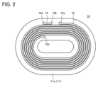
- FIG. FIG. 2 is a plan view of the printed wiring board 10.
- FIG. FIG. 3 is a bottom view of the printed wiring board 10.
- FIG. FIG. 4 is a plan view of printed wiring board 10 for explaining the area of the first coil.
- FIG. 5 is a cross-sectional view of a coil device 100 according to a modification.
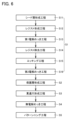
- 6A to 6D are process diagrams showing a method of manufacturing the coil device 100.
- FIG. FIG. 7 is a cross-sectional view for explaining the seed layer forming step S11.
- FIG. 8 is a cross-sectional view for explaining the resist forming step S12.
- FIG. 9 is a cross-sectional view for explaining the first electroplating step S13.
- FIG. 10 is a cross-sectional view for explaining the resist removing step S14.
- FIG. 11 is a cross-sectional view for explaining the etching step S15.
- FIG. 12 is a cross-sectional view for explaining the second electroplating step S16.
- FIG. 13 is a cross-sectional view for explaining the protective layer forming step S2.
- FIG. 14 is a cross-sectional view for explaining the through-hole forming step S3.
- FIG. 15 is a cross-sectional view for explaining the electroless plating step S4.
- the present disclosure has been made in view of the problems of the prior art as described above. More specifically, the present disclosure provides a coil system capable of improved thrust.
- a coil device has a first surface and a second surface, which are end surfaces in the thickness direction of the coil device.
- the coil device includes at least one printed wiring board, a first protective layer, and external connection terminals.
- Each of the at least one printed wiring board includes a first base film including a first main surface and a second main surface opposite to the first main surface, and a second base film spirally formed on the first main surface. It has 1 coil wiring and the 2nd coil wiring formed spirally on the 2nd main surface.
- the first protective layer covers the first main surface of one of the at least one printed wiring board that is arranged closest to the first surface.
- the external connection terminal is formed on the first protective layer and electrically connected to the first coil wiring.
- the coil device of (1) further electrically connects the first coil wiring of one of the at least one printed wiring board arranged closest to the first surface and the external connection terminal.
- a conductive layer may be provided.
- a through hole penetrating through the first protective layer may be formed in the first protective layer.
- the through-hole may partially expose one first coil wire of the at least one printed wiring board arranged closest to the first surface.
- the conductive layer may be formed on the first coil wiring exposed from the through hole and on the inner wall surface of the through hole.
- the coil device of (1) or (2) may further comprise at least one first adhesive layer.
- the at least one printed wiring board may be a plurality of printed wiring boards.
- At least one first adhesive layer may be disposed between two adjacent ones of the plurality of printed wiring boards.
- the number of printed wiring boards may be two or three.
- the first protective layer covers the first major surface of one of the at least one printed wiring board located closest to the first surface. and a second base film disposed on the second adhesive layer.
- the coil devices of (1) to (5) may further include a second protective layer.
- the second protective layer may cover the second major surface of one of the at least one printed wiring board located closest to the second surface.
- the second protective layer covers the second major surface of one of the at least one printed wiring board located closest to the second surface. and a third base film disposed on the third adhesive layer.
- the thickness of the first protective layer is 5 ⁇ m or more and 50 ⁇ m or less, and 0.8 times or more and 1.2 times or less of the thickness of the second protective layer.
- the value obtained by dividing the area of the coil configured by the first coil wiring by the area of the first main surface and the area of the coil configured by the second coil wiring At least one of the values obtained by dividing the area by the area of the second main surface may be 0.40 or more and 0.90 or less.
- the value obtained by dividing the area of the coil configured by the first coil wiring by the area of the first main surface and the area of the coil configured by the second coil wiring At least one of the values obtained by dividing the area by the area of the second main surface may be 0.60 or more and 0.90 or less.
- the width of the first coil wiring and the width of the second coil wiring may be 20 ⁇ m or more and 40 ⁇ m or less.
- the thickness of the first coil wiring and the thickness of the second coil wiring may be 30 ⁇ m or more and 70 ⁇ m or less.
- a distance between two adjacent portions of the first coil wiring and a distance between two adjacent portions of the second coil wiring may be 3 ⁇ m or more and 15 ⁇ m or less.
- the value obtained by dividing the area of the coil configured by the first coil wiring by the area of the first main surface is the coil configured by the second coil wiring. 0.95 times or more and 1.05 times or less of the value obtained by dividing the area of by the area of the second main surface.
- a printed wiring board includes a first base film having a first main surface and a second main surface opposite to the first main surface, and a spirally formed base film on the first main surface. and a second coil wiring spirally formed on the second main surface. At least one of a value obtained by dividing the area of the coil formed by the first coil wiring by the area of the first main surface and a value obtained by dividing the area of the coil formed by the second coil wiring by the area of the second main surface is between 0.40 and 0.90.
- the printed wiring board (13) it is possible to improve thrust when used in a coil device.
- the value obtained by dividing the area of the coil formed by the first coil wiring by the area of the first main surface and the area of the coil formed by the second coil wiring are the At least one of the values divided by the areas of the two main surfaces may be 0.60 or more and 0.90.
- the value obtained by dividing the area of the coil formed by the first coil wiring by the area of the first main surface is formed by the second coil wiring. It may be 0.95 to 1.05 times the value obtained by dividing the area of the coil by the area of the second main surface.
- a printed wiring board includes a first base film having a first main surface and a second main surface opposite to the first main surface, and a base film spirally formed on the first main surface. and a second coil wiring spirally formed on the second main surface.
- the value obtained by dividing the width of the first coil wiring by the pitch between two portions of the adjacent first coil wiring and the width of the second coil wiring between the two portions of the adjacent second coil wiring is 0.72 or more and 0.93 or less.
- the printed wiring board (16) it is possible to improve thrust when used in a coil device.
- a coil device according to the embodiment is referred to as a coil device 100 .
- FIG. 1 is a cross-sectional view of the coil device 100.
- FIG. FIG. 2 is a plan view of the printed wiring board 10.
- FIG. FIG. 3 is a bottom view of the printed wiring board 10.
- FIG. FIG. 3 shows printed wiring board 10 viewed from the opposite side to FIG.
- the coil device 100 includes a printed wiring board 10, a first protective layer 20, a second protective layer 30, external connection terminals 40, and a conductive layer 50. have.
- the coil device 100 has a first surface 100a and a second surface 100b.
- the first surface 100a and the second surface 100b are end surfaces of the coil device 100 in the thickness direction.
- the second surface 100b is the opposite surface of the first surface 100a.
- the printed wiring board 10 has a base film 11 , a first coil wiring 12 , a second coil wiring 13 and a connection wiring 14 .
- the base film 11 has a first main surface 11a and a second main surface 11b.
- the first main surface 11a and the second main surface 11b are end surfaces of the base film 11 in the thickness direction.
- the base film 11 is made of a flexible, electrically insulating material.
- the base film 11 is made of, for example, polyimide, polyethylene terephthalate, or fluororesin.
- the first coil wiring 12 is arranged on the first main surface 11a.
- the first coil wiring 12 is spirally wound in plan view.
- the second coil wiring 13 is arranged on the second main surface 11b.
- the second coil wiring 13 is spirally wound in plan view.
- the connection wiring 14 is arranged on the first main surface 11a.
- One end and the other end of the first coil wiring 12 are lands 12a and 12b, respectively.
- One ends of the second coil wiring 13 are lands 13a and 13b, respectively.
- One end and the other end of the connection wiring 14 are lands 14a and 14b, respectively.
- the land 12b and the land 13a overlap each other in plan view.
- the land 13b and the land 14a overlap each other in plan view.
- the base film 11 is formed with a through hole 11c (not shown) and a through hole 11d (not shown) penetrating the base film 11 along the thickness direction.
- the through hole 11c overlaps the land 12b and the land 13a in plan view.
- the through hole 11d overlaps the land 13b and the land 14a in plan view.
- the first coil wiring 12 and the second coil wiring 13 are electrically connected to each other by a conductive layer 11e (not shown) formed on the inner wall surface of the through hole 11c.
- the second coil wire 13 and the connection wire 14 are electrically connected to each other by a conductive layer 11f (not shown) formed on the inner wall surface of the through hole 11d.
- Each of the first coil wiring 12 and the second coil wiring 13 has a seed layer 15 , a first electroplating layer 16 and a second electroplating layer 17 .
- the seed layer 15 is arranged on the main surfaces of the base film 11 (the first main surface 11a and the second main surface 11b).
- the seed layer 15 has a first layer 15a and a second layer 15b.
- the first layer 15a is arranged on the main surfaces (first main surface 11a, second main surface 11b) of the base film 11 .
- the second layer 15b is arranged on the first layer 15a.
- the first layer 15a is, for example, a sputtered layer (a layer formed by sputtering) made of a nickel-chromium alloy.
- the second layer 15b is an electroless plated layer (layer formed by electroless plating) made of copper, for example.
- the first electroplating layer 16 is arranged on the seed layer 15 .
- the first electrolytic plated layer 16 is an electrolytic plated layer made of copper.
- the second electroplating layer 17 covers the seed layer 15 and the first electroplating layer 16 . More specifically, the second electrolytic plated layer 17 is arranged on the side surfaces of the seed layer 15 and on the side surfaces and the upper surface of the first electrolytic plated layer 16 .
- a coil configured by the first coil wiring 12 is referred to as a first coil.
- a coil configured by the second coil wiring 13 is referred to as a second coil.
- At least one of the area ratio of the first coil and the area ratio of the second coil is preferably 0.40 or more and 0.90 or less.
- At least one of the area ratio of the first coil and the area ratio of the second coil is more preferably 0.60 or more and 0.90 or less.
- the area ratio of the first coil is preferably 0.95 to 1.05 times the area ratio of the second coil.
- the area ratio of the first coil is a value obtained by dividing the area of the first coil by the area of the first main surface 11a
- the area ratio of the second coil is obtained by dividing the area of the second coil by the area of the second main surface 11b. value.
- the area of the first coil is the sum of the area of the first coil wire 12 and the area of the first main surface 11a between two portions of the first coil wire 12 adjacent to each other.
- the area of the second coil is the sum of the area of the second coil wire 13 and the area of the second main surface 11b between two portions of the second coil wire 13 adjacent to each other.
- the area of the first coil wiring 12 is the area of the first coil wiring 12 in plan view from the first main surface 11a side. That is, the area of the first coil wiring 12 does not include the side surface area of the first coil wiring 12 .
- the area of the second coil wiring 13 is the area of the second coil wiring 13 in a plan view seen from the second main surface 11b side. That is, the area of the second coil wiring 13 does not include the side surface area of the second coil wiring 13 .
- FIG. 4 is a plan view of the printed wiring board 10 explaining the area of the first coil. As shown in FIG. 4, the area of the first main surface 11a (cross-hatched portion in FIG. 4) other than between two portions of the adjacent first coil wiring 12 is the area of the first coil. is not included. Although not shown, the second main surface 11b other than between two portions of the second coil wiring 13 adjacent to each other is also not included in the area of the second coil.
- the width of the first coil wiring 12 is assumed to be W1, and the width of the second coil wiring 13 is assumed to be W2.
- the width W1 and the width W2 are preferably 20 ⁇ m or more and 40 ⁇ m or less.
- the thickness of the first coil wiring 12 is assumed to be thickness T1.
- the thickness of the second coil wiring 13 is assumed to be thickness T2.
- the thickness T1 and the thickness T2 are preferably 30 ⁇ m or more and 70 ⁇ m or less.
- a distance between two adjacent portions of the first coil wiring 12 is defined as a distance L1.
- a distance between two adjacent portions of the second coil wiring 13 is defined as a distance L2.
- the distance L1 and the distance L2 are preferably 3 ⁇ m or more and 15 ⁇ m or less.
- the pitch between two adjacent portions of the first coil wiring 12 is defined as a pitch P1.
- a pitch between two adjacent portions of the second coil wiring 13 is defined as a pitch P2.
- the value obtained by dividing the width W1 by the pitch P1 and the value obtained by dividing the width W2 by the pitch P2 are preferably 0.72 or more and 0.93 or less.
- the first protective layer 20 covers the first main surface 11a.
- the first protective layer 20 has an adhesive layer 21 and a base film 22 .
- the adhesive layer 21 covers the first main surface 11a.
- a base film 22 is arranged on the adhesive layer 21 .
- the adhesive layer 21 is made of, for example, an adhesive.
- the base film 22 is made of polyimide, polyethylene terephthalate, or fluorine resin, for example.
- a through hole 20 a is formed in the first protective layer 20 .
- the through hole 20a penetrates the first protective layer 20 along the thickness direction and partially exposes the first coil wiring 12 .
- the land 12a is exposed from the through hole 20a.
- the thickness of the first protective layer 20 is assumed to be thickness T3.
- the thickness T3 is the distance between the top surface of the first coil wire 12 and the surface of the first protective layer 20 .
- the thickness T3 is preferably 5 ⁇ m or more and 50 ⁇ m or less.
- the second protective layer 30 covers the second main surface 11b.
- the second protective layer 30 has an adhesive layer 31 and a base film 32 .
- the adhesive layer 31 covers the second main surface 11b.
- a base film 32 is arranged on the adhesive layer 31 .
- the adhesive layer 31 is made of, for example, an adhesive.
- the base film 32 is made of polyimide, polyethylene terephthalate, or fluorine resin, for example.
- the thickness of the second protective layer 30 is assumed to be thickness T4.
- the thickness T4 is the distance between the top surface of the second coil wire 13 and the surface of the second protective layer 30 .
- the thickness T4 is preferably 5 ⁇ m or more and 50 ⁇ m or less.
- the thickness T3 is preferably 0.8 to 1.2 times the thickness T4.
- the external connection terminals 40 are arranged on the first protective layer 20 (base film 22).
- the external connection terminals 40 are made of copper, for example.
- the conductive layer 50 is an electroless plated layer made of copper, for example.
- the conductive layer 50 is arranged on the portion (for example, the land 12a) of the first coil wire 12 exposed from the through hole 20a and on the inner wall surface of the through hole 20a.
- the conductive layer 50 is also arranged on the external connection terminals 40 . Therefore, the conductive layer 50 electrically connects the external connection terminal 40 and the first coil wiring 12 .
- through holes 20b are formed in the first protective layer 20 in addition to the through holes 20a for exposing the lands 14b.
- An external connection terminal 41 is arranged.
- a conductive layer 51 (not shown) separate from the conductive layer 50 is arranged on the inner wall surface of the through hole 20b, on the land 14b, and on the external connection terminal 41, so that the external connection terminal 41 can be used as a connection wiring. 14 are electrically connected.
- connection wiring 14 is electrically connected to the second coil wiring 13 , and the second coil wiring 13 is connected to the first coil wiring 12 to the electric house. By applying a voltage between them, a current flows through the first coil wiring 12 and the second coil wiring 13, and the first coil and the second coil generate a magnetic field.
- FIG. 5 is a cross-sectional view of a coil device 100 according to a modification.
- the coil device 100 may have multiple printed wiring boards 10 .
- the number of printed wiring boards 10 is preferably two or three. In this case, two printed wiring boards 10 that are adjacent in the thickness direction of coil device 100 are adhered to each other by adhesive layer 60 .
- the first protective layer 20 covers the first main surface 11a of the printed wiring board 10 closest to the first surface 100a
- the second protective layer 30 is closest to the second surface 100b. It covers the second main surface 11 b of the printed wiring board 10 .
- FIG. 6 is a process diagram showing a method of manufacturing the coil device 100.
- the method of manufacturing the coil device 100 includes a printed wiring board forming step S1, a protective layer forming step S2, a through hole forming step S3, an electroless plating step S4, and a patterning step S5. have.
- the printed wiring board forming step S1 includes a seed layer forming step S11, a resist forming step S12, a first electrolytic plating step S13, a resist removing step S14, an etching step S15, and a second electrolytic plating step S16. ing.
- FIG. 7 is a cross-sectional view for explaining the seed layer forming step S11.
- the seed layer 15 first layer 15a, second layer 15b
- the first layer 15a is formed on the first major surface 11a and the second major surface 11b.
- the first layer 15a is formed by sputtering, for example.
- through holes 11c and 11d are formed.
- the through holes 11c and 11d are formed by, for example, irradiating laser light.
- the second layer 15b is formed on the first layer 15a. Although not shown, the second layer 15b is also formed on the inner wall surfaces of the through holes 11c and 11d.
- the second layer 15b is formed by, for example, electroless plating.
- FIG. 8 is a cross-sectional view for explaining the resist forming step S12.
- a resist 70 is formed in the resist forming step S12.
- the resist 70 is formed, for example, by applying a dry film resist onto the seed layer 15 and patterning the applied dry film resist by exposing and developing it.
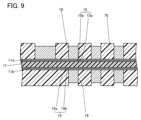
- FIG. 9 is a cross-sectional view for explaining the first electroplating step S13.
- the first electroplating layer 16 is formed on the seed layer 15 exposed from the resist 70. As shown in FIG. although not shown, it is also formed on the second layer 15b on the inner wall surfaces of the through holes 11c and 11d.
- the first electrolytic plated layer 16 is formed by energizing the seed layer 15 in a plating solution containing the constituent material of the first electrolytic plated layer 16 .
- FIG. 10 is a cross-sectional view for explaining the resist removing step S14. As shown in FIG. 10, in the resist removing step S14, the resist 70 is removed by peeling.
- FIG. 11 is a cross-sectional view for explaining the etching step S15. As shown in FIG. 11, in the etching step S15, the seed layer 15 exposed between two adjacent portions of the first electroplating layer 16 is removed by etching.
- the second layer 15b is etched. Etching of the second layer 15b is performed by supplying an etchant between two adjacent portions of the first electroplating layer 16 .
- the etchant is selected so that etching is rate-determined by the reaction between the reactive species in the etchant and the object to be etched rather than the diffusion of the reactive species in the etchant to the vicinity of the object to be etched.
- the etchant used is an etchant that has a dissolution reaction rate of 1.0 ⁇ m/min or less for the material (that is, copper) forming the second layer 15b.
- the etching solution include sulfuric acid hydrogen peroxide aqueous solution and sodium peroxodisulfate aqueous solution. The dissolution reaction rate of the etchant is measured based on the weight of copper reduced after etching and the etching time.
- the first layer 15a is etched.
- the etchant is switched when the etching of the first layer 15a is performed.
- an etchant having a high selectivity with respect to the material (that is, nickel-chromium alloy) forming the first layer 15a is used. Therefore, after switching the etchant, the etching of the first electroplating layer 16 is difficult to proceed.
- FIG. 12 is a cross-sectional view for explaining the second electroplating step S16.
- the second electroplating layer 17 is formed so as to cover the seed layer 15 and the first electroplating layer 16.
- the second electrolytic plated layer 17 is also formed on the first electrolytic plated layer 16 on the inner wall surfaces of the through holes 11c and 11d with the second layer 15b interposed therebetween.
- the conductive layers 11e and 11f are composed of the second layer 15b, the first electrolytic plated layer 16 and the second electrolytic plated layer 17. As shown in FIG.
- the second electroplating layer 17 is formed by energizing the seed layer 15 and the first electroplating layer 16 in the plating solution containing the constituent materials of the second electroplating layer 17 .
- the printed wiring board 10 is formed using the semi-additive method.
- FIG. 13 is a cross-sectional view for explaining the protective layer forming step S2.
- the first protective layer 20 is formed on the first main surface 11a
- the second protective layer 30 is formed on the second main surface 11b.
- the base film 22 coated with the adhesive layer 21 is arranged on the first main surface 11a so as to cover the first coil wiring 12, and the adhesive layer 31 is applied.
- a base film 32 is arranged on the second main surface 11 b so as to cover the second coil wiring 13 .
- the adhesive layer 21 and the adhesive layer 31 are uncured.
- the base film 22 and the base film 32 are pressed toward the base film 11 while being heated. Thereby, the adhesive layer 21 and the adhesive layer 31 are cured, and the base film 22 and the base film 32 are attached.
- the copper layer 23 is arranged on the base film 22 and the copper layer 33 is arranged on the base film 32 when the protective layer forming step S2 is performed.
- FIG. 14 is a cross-sectional view explaining the through-hole forming step S3.
- through holes 20a are formed in the first protective layer 20 in the through hole forming step S3.
- the through hole 20a is formed by, for example, irradiating laser light.
- the through hole 20b is also formed in the same manner.
- FIG. 15 is a cross-sectional view explaining the electroless plating step S4.
- an electroless plated layer 24 is formed on the copper layer 23, and an electroless plated layer 34 is formed on the copper layer 33.
- the electroless plated layer 24 and the electroless plated layer 34 contain the constituent materials of the electroless plated layer 24 and the electroless plated layer 34 of the printed wiring board 10 on which the first protective layer 20 and the second protective layer 30 are formed. It is performed by immersion in a plating solution.
- the external connection terminals 40 and the conductive layer 50 are formed by patterning the copper layer 23 and the electroless plated layer 24 .
- the external connection terminals 41 and the conductive layer 51 are also formed along with the patterning of the copper layer 23 and the electroless plated layer 24 .
- Patterning of the copper layer 23 and the electroless plated layer 24 is performed by applying, for example, a dry film resist on the electroless plated layer 24, exposing and developing the applied dry film resist to form a resist, and masking the resist. This is carried out by etching the copper layer 23 and the electroless plated layer 24 as a layer. Since no resist is formed on the electroless plated layer 34, the copper layer 33 and the electroless plated layer 34 are all removed by the above etching. As described above, the coil device 100 having the structure shown in FIG. 1 is formed.
- the external connection terminals 40 and the external connection terminals 41 it is conceivable to arrange the external connection terminals 40 and the external connection terminals 41 on the first main surface 11a.
- the external connection terminals 40 and 41 are arranged on the first main surface 11a, the area of the first main surface 11a on which the first coil wiring 12 can be arranged is reduced. As a result, the area ratio of the first coil becomes smaller than the area ratio of the second coil.
- the area of the first main surface 11a on which the first coil wiring 12 can be arranged is It never decreases. Therefore, in the coil device 100, the area ratio of the first coil can be made approximately the same as the area ratio of the second coil, and the thrust of the coil device 100 can be increased.
- an etchant with a high dissolution reaction rate for the material forming the seed layer that is, an etchant in which the diffusion of the reactive species in the etchant to the vicinity of the etching target determines the etching rate
- an etchant with a high dissolution reaction rate for the material forming the seed layer that is, an etchant in which the diffusion of the reactive species in the etchant to the vicinity of the etching target determines the etching rate
- the etching in the etching step S15 is rate-determined by the reaction between the reactive species in the etching solution and the object to be etched, and the etching solution is supplied between two adjacent portions of the first electroplating layer 16. Even if it is difficult to etch the second layer 15b, variations in etching are unlikely to occur.
- the distance between two adjacent portions of the first coil wiring 12 (second coil wiring 13) can be shortened, and the first coil wiring 12 (second coil wiring 13) can be shortened. 13) can be increased in thickness.
- the area ratio of the first coil and the area ratio of the second coil can be increased, and the thrust of the coil device 100 can be increased.
- the width of the first coil wiring 12 (second coil wiring 13) can be increased. can. Therefore, according to the printed wiring board 10, the thickness and width of the first coil wiring 12 (second coil wiring 13) can be increased, and the electrical resistance value of the first coil wiring 12 (second coil wiring 13) can be increased to become smaller. As a result, it is possible to suppress an increase in the electrical resistance value accompanying an increase in the area ratio of the first coil and the area ratio of the second coil.
Landscapes
- Engineering & Computer Science (AREA)
- Microelectronics & Electronic Packaging (AREA)
- Power Engineering (AREA)
- Manufacturing & Machinery (AREA)
- Coils Or Transformers For Communication (AREA)
Priority Applications (4)
| Application Number | Priority Date | Filing Date | Title |
|---|---|---|---|
| KR1020247021693A KR20240132015A (ko) | 2022-01-05 | 2022-12-23 | 코일 장치 및 프린트 배선판 |
| JP2023572439A JPWO2023132278A1 (https=) | 2022-01-05 | 2022-12-23 | |
| CN202280087403.7A CN118511233A (zh) | 2022-01-05 | 2022-12-23 | 线圈装置及印刷布线板 |
| US18/723,739 US20250107001A1 (en) | 2022-01-05 | 2022-12-23 | Coil device and printed wiring board |
Applications Claiming Priority (4)
| Application Number | Priority Date | Filing Date | Title |
|---|---|---|---|
| JP2022000509 | 2022-01-05 | ||
| JP2022-000509 | 2022-01-05 | ||
| JP2022020717 | 2022-02-14 | ||
| JP2022-020717 | 2022-02-14 |
Publications (1)
| Publication Number | Publication Date |
|---|---|
| WO2023132278A1 true WO2023132278A1 (ja) | 2023-07-13 |
Family
ID=87073623
Family Applications (1)
| Application Number | Title | Priority Date | Filing Date |
|---|---|---|---|
| PCT/JP2022/047696 Ceased WO2023132278A1 (ja) | 2022-01-05 | 2022-12-23 | コイル装置及びプリント配線板 |
Country Status (5)
| Country | Link |
|---|---|
| US (1) | US20250107001A1 (https=) |
| JP (1) | JPWO2023132278A1 (https=) |
| KR (1) | KR20240132015A (https=) |
| TW (1) | TW202348101A (https=) |
| WO (1) | WO2023132278A1 (https=) |
Cited By (3)
| Publication number | Priority date | Publication date | Assignee | Title |
|---|---|---|---|---|
| WO2025126816A1 (ja) * | 2023-12-11 | 2025-06-19 | 住友電気工業株式会社 | プリント配線板 |
| WO2025146739A1 (ja) * | 2024-01-04 | 2025-07-10 | 住友電工プリントサーキット株式会社 | コイル装置及びコイル装置の製造方法 |
| WO2025146738A1 (ja) * | 2024-01-04 | 2025-07-10 | 住友電気工業株式会社 | コイル装置及びアクチュエータ |
Citations (2)
| Publication number | Priority date | Publication date | Assignee | Title |
|---|---|---|---|---|
| JP2016136556A (ja) * | 2015-01-23 | 2016-07-28 | イビデン株式会社 | インダクタ部品及びプリント配線板 |
| WO2020175476A1 (ja) * | 2019-02-27 | 2020-09-03 | 住友電工プリントサーキット株式会社 | プリント配線板及びプリント配線板の製造方法 |
Family Cites Families (1)
| Publication number | Priority date | Publication date | Assignee | Title |
|---|---|---|---|---|
| JP6311200B2 (ja) | 2014-06-26 | 2018-04-18 | 住友電工プリントサーキット株式会社 | プリント配線板、電子部品及びプリント配線板の製造方法 |
-
2022
- 2022-12-23 JP JP2023572439A patent/JPWO2023132278A1/ja active Pending
- 2022-12-23 KR KR1020247021693A patent/KR20240132015A/ko active Pending
- 2022-12-23 WO PCT/JP2022/047696 patent/WO2023132278A1/ja not_active Ceased
- 2022-12-23 US US18/723,739 patent/US20250107001A1/en active Pending
-
2023
- 2023-01-03 TW TW112100040A patent/TW202348101A/zh unknown
Patent Citations (2)
| Publication number | Priority date | Publication date | Assignee | Title |
|---|---|---|---|---|
| JP2016136556A (ja) * | 2015-01-23 | 2016-07-28 | イビデン株式会社 | インダクタ部品及びプリント配線板 |
| WO2020175476A1 (ja) * | 2019-02-27 | 2020-09-03 | 住友電工プリントサーキット株式会社 | プリント配線板及びプリント配線板の製造方法 |
Cited By (3)
| Publication number | Priority date | Publication date | Assignee | Title |
|---|---|---|---|---|
| WO2025126816A1 (ja) * | 2023-12-11 | 2025-06-19 | 住友電気工業株式会社 | プリント配線板 |
| WO2025146739A1 (ja) * | 2024-01-04 | 2025-07-10 | 住友電工プリントサーキット株式会社 | コイル装置及びコイル装置の製造方法 |
| WO2025146738A1 (ja) * | 2024-01-04 | 2025-07-10 | 住友電気工業株式会社 | コイル装置及びアクチュエータ |
Also Published As
| Publication number | Publication date |
|---|---|
| JPWO2023132278A1 (https=) | 2023-07-13 |
| KR20240132015A (ko) | 2024-09-02 |
| TW202348101A (zh) | 2023-12-01 |
| US20250107001A1 (en) | 2025-03-27 |
Similar Documents
| Publication | Publication Date | Title |
|---|---|---|
| WO2023132278A1 (ja) | コイル装置及びプリント配線板 | |
| US5759417A (en) | Flexible circuit board and production method therefor | |
| JP4558776B2 (ja) | 回路基板の製造方法 | |
| US7569773B2 (en) | Wired circuit board | |
| US5366794A (en) | Tape carrier for semiconductor apparatus | |
| CN110073729A (zh) | 配线基板、多层配线基板以及配线基板的制造方法 | |
| JPWO2023132278A5 (https=) | ||
| EP0147566B1 (en) | Method of forming contacts for flexible module carriers | |
| JP7464352B2 (ja) | 配線基板およびその製造方法 | |
| CN115190701A (zh) | 一种埋入式线路封装基板及其加工方法 | |
| KR20040023773A (ko) | 도체 배선 패턴의 형성 방법 | |
| CN118511233A (zh) | 线圈装置及印刷布线板 | |
| JP7563600B2 (ja) | プリント配線板 | |
| JP2023037405A (ja) | 配線基板 | |
| WO2023132262A1 (ja) | コイル装置及びプリント配線板 | |
| JP7629102B2 (ja) | プリント配線板 | |
| JP2006310758A (ja) | 回路配線板、及びその製造方法 | |
| CN114641136A (zh) | 电路板的铜层凸台制作方法及电路板 | |
| WO2023276817A1 (ja) | プリント配線板 | |
| JP7400989B2 (ja) | コイル装置 | |
| JP2005108941A (ja) | 多層配線板及びその製造方法 | |
| CN118475994A (zh) | 线圈装置及印刷布线板 | |
| JP2025007792A (ja) | 配線基板 | |
| JP2795475B2 (ja) | プリント配線板及びその製造方法 | |
| US9668340B1 (en) | Methods and devices for preventing overhangs in a finishing layer of metal formed on electrical contact surfaces when fabricating multi-layer printed circuit boards |
Legal Events
| Date | Code | Title | Description |
|---|---|---|---|
| 121 | Ep: the epo has been informed by wipo that ep was designated in this application |
Ref document number: 22918862 Country of ref document: EP Kind code of ref document: A1 |
|
| WWE | Wipo information: entry into national phase |
Ref document number: 18723739 Country of ref document: US |
|
| WWE | Wipo information: entry into national phase |
Ref document number: 2023572439 Country of ref document: JP |
|
| WWE | Wipo information: entry into national phase |
Ref document number: 202280087403.7 Country of ref document: CN |
|
| NENP | Non-entry into the national phase |
Ref country code: DE |
|
| 122 | Ep: pct application non-entry in european phase |
Ref document number: 22918862 Country of ref document: EP Kind code of ref document: A1 |
|
| WWP | Wipo information: published in national office |
Ref document number: 18723739 Country of ref document: US |