WO2023132278A1 - Coil device and printed wiring board - Google Patents
Coil device and printed wiring board Download PDFInfo
- Publication number
- WO2023132278A1 WO2023132278A1 PCT/JP2022/047696 JP2022047696W WO2023132278A1 WO 2023132278 A1 WO2023132278 A1 WO 2023132278A1 JP 2022047696 W JP2022047696 W JP 2022047696W WO 2023132278 A1 WO2023132278 A1 WO 2023132278A1
- Authority
- WO
- WIPO (PCT)
- Prior art keywords
- coil
- main surface
- area
- wiring
- layer
- Prior art date
Links
- 239000011241 protective layer Substances 0.000 claims abstract description 60
- 239000010410 layer Substances 0.000 claims description 131
- 239000012790 adhesive layer Substances 0.000 claims description 26
- 230000000149 penetrating effect Effects 0.000 claims description 3
- 238000009713 electroplating Methods 0.000 description 27
- 238000005530 etching Methods 0.000 description 27
- RYGMFSIKBFXOCR-UHFFFAOYSA-N Copper Chemical compound [Cu] RYGMFSIKBFXOCR-UHFFFAOYSA-N 0.000 description 17
- 229910052802 copper Inorganic materials 0.000 description 17
- 239000010949 copper Substances 0.000 description 17
- 238000007772 electroless plating Methods 0.000 description 8
- 239000000463 material Substances 0.000 description 7
- 238000000059 patterning Methods 0.000 description 7
- 239000000243 solution Substances 0.000 description 6
- 238000004519 manufacturing process Methods 0.000 description 5
- 238000000034 method Methods 0.000 description 5
- 238000004090 dissolution Methods 0.000 description 4
- 230000004048 modification Effects 0.000 description 4
- 238000012986 modification Methods 0.000 description 4
- 238000007747 plating Methods 0.000 description 4
- 239000004642 Polyimide Substances 0.000 description 3
- 239000000470 constituent Substances 0.000 description 3
- 230000000694 effects Effects 0.000 description 3
- -1 polyethylene terephthalate Polymers 0.000 description 3
- 229920000139 polyethylene terephthalate Polymers 0.000 description 3
- 239000005020 polyethylene terephthalate Substances 0.000 description 3
- 229920001721 polyimide Polymers 0.000 description 3
- YCKRFDGAMUMZLT-UHFFFAOYSA-N Fluorine atom Chemical compound [F] YCKRFDGAMUMZLT-UHFFFAOYSA-N 0.000 description 2
- 239000000853 adhesive Substances 0.000 description 2
- 230000001070 adhesive effect Effects 0.000 description 2
- 239000007864 aqueous solution Substances 0.000 description 2
- 230000007423 decrease Effects 0.000 description 2
- 238000010586 diagram Methods 0.000 description 2
- 238000009792 diffusion process Methods 0.000 description 2
- 229910052731 fluorine Inorganic materials 0.000 description 2
- 239000011737 fluorine Substances 0.000 description 2
- 230000001678 irradiating effect Effects 0.000 description 2
- 229910000623 nickel–chromium alloy Inorganic materials 0.000 description 2
- 239000011347 resin Substances 0.000 description 2
- 229920005989 resin Polymers 0.000 description 2
- CHQMHPLRPQMAMX-UHFFFAOYSA-L sodium persulfate Chemical compound [Na+].[Na+].[O-]S(=O)(=O)OOS([O-])(=O)=O CHQMHPLRPQMAMX-UHFFFAOYSA-L 0.000 description 2
- 238000004544 sputter deposition Methods 0.000 description 2
- 239000000654 additive Substances 0.000 description 1
- 230000015572 biosynthetic process Effects 0.000 description 1
- 239000012777 electrically insulating material Substances 0.000 description 1
- XEMZLVDIUVCKGL-UHFFFAOYSA-N hydrogen peroxide;sulfuric acid Chemical compound OO.OS(O)(=O)=O XEMZLVDIUVCKGL-UHFFFAOYSA-N 0.000 description 1
- 238000007654 immersion Methods 0.000 description 1
- 230000000873 masking effect Effects 0.000 description 1
- 238000004904 shortening Methods 0.000 description 1
Images


Classifications
-
- H—ELECTRICITY
- H01—ELECTRIC ELEMENTS
- H01F—MAGNETS; INDUCTANCES; TRANSFORMERS; SELECTION OF MATERIALS FOR THEIR MAGNETIC PROPERTIES
- H01F17/00—Fixed inductances of the signal type
-
- H—ELECTRICITY
- H01—ELECTRIC ELEMENTS
- H01F—MAGNETS; INDUCTANCES; TRANSFORMERS; SELECTION OF MATERIALS FOR THEIR MAGNETIC PROPERTIES
- H01F17/00—Fixed inductances of the signal type
- H01F17/02—Fixed inductances of the signal type without magnetic core
-
- H—ELECTRICITY
- H01—ELECTRIC ELEMENTS
- H01F—MAGNETS; INDUCTANCES; TRANSFORMERS; SELECTION OF MATERIALS FOR THEIR MAGNETIC PROPERTIES
- H01F27/00—Details of transformers or inductances, in general
- H01F27/28—Coils; Windings; Conductive connections
-
- H—ELECTRICITY
- H01—ELECTRIC ELEMENTS
- H01F—MAGNETS; INDUCTANCES; TRANSFORMERS; SELECTION OF MATERIALS FOR THEIR MAGNETIC PROPERTIES
- H01F27/00—Details of transformers or inductances, in general
- H01F27/28—Coils; Windings; Conductive connections
- H01F27/29—Terminals; Tapping arrangements for signal inductances
-
- H—ELECTRICITY
- H05—ELECTRIC TECHNIQUES NOT OTHERWISE PROVIDED FOR
- H05K—PRINTED CIRCUITS; CASINGS OR CONSTRUCTIONAL DETAILS OF ELECTRIC APPARATUS; MANUFACTURE OF ASSEMBLAGES OF ELECTRICAL COMPONENTS
- H05K1/00—Printed circuits
- H05K1/16—Printed circuits incorporating printed electric components, e.g. printed resistor, capacitor, inductor
Definitions
- the present disclosure relates to a coil device and a printed wiring board.
- This application has priority based on Japanese Patent Application No. 2022-509 filed on January 5, 2022 and Japanese Patent Application No. 2022-020717 filed on February 14, 2022. claim priority under All the contents described in the Japanese patent application are incorporated herein by reference.
- Patent Document 1 Japanese Patent Application Laid-Open No. 2016-9854
- Patent Document 1 Japanese Patent Application Laid-Open No. 2016-9854
- the printed wiring board described in Patent Document 1 has a base film and wiring.
- the base film has a first major surface and a second major surface opposite to the first major surface.
- the wiring has a first wiring arranged on the first main surface and a second wiring arranged on the second main surface.
- the first wiring and the second wiring are electrically connected to each other via a plating layer arranged on the inner wall surface of the through hole formed in the base film.
- the first wiring and the second wiring constitute a coil by being spirally wound.
- the coil device of the present disclosure has a first surface and a second surface, which are end surfaces in the thickness direction of the coil device.
- the coil device includes at least one printed wiring board, a first protective layer, and external connection terminals.
- Each of the at least one printed wiring board includes a first base film including a first main surface and a second main surface opposite to the first main surface, and a second base film spirally formed on the first main surface. It has 1 coil wiring and the 2nd coil wiring formed spirally on the 2nd main surface.
- the first protective layer covers the first main surface of one of the at least one printed wiring board that is arranged closest to the first surface.
- the external connection terminal is formed on the first protective layer and electrically connected to the first coil wiring.
- FIG. 1 is a cross-sectional view of the coil device 100.
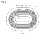
- FIG. FIG. 2 is a plan view of the printed wiring board 10.
- FIG. FIG. 3 is a bottom view of the printed wiring board 10.
- FIG. FIG. 4 is a plan view of printed wiring board 10 for explaining the area of the first coil.
- FIG. 5 is a cross-sectional view of a coil device 100 according to a modification.
- 6A to 6D are process diagrams showing a method of manufacturing the coil device 100.
- FIG. FIG. 7 is a cross-sectional view for explaining the seed layer forming step S11.
- FIG. 8 is a cross-sectional view for explaining the resist forming step S12.
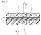
- FIG. 9 is a cross-sectional view for explaining the first electroplating step S13.
- FIG. 10 is a cross-sectional view for explaining the resist removing step S14.
- FIG. 11 is a cross-sectional view for explaining the etching step S15.
- FIG. 12 is a cross-sectional view for explaining the second electroplating step S16.
- FIG. 13 is a cross-sectional view for explaining the protective layer forming step S2.
- FIG. 14 is a cross-sectional view for explaining the through-hole forming step S3.
- FIG. 15 is a cross-sectional view for explaining the electroless plating step S4.
- the present disclosure has been made in view of the problems of the prior art as described above. More specifically, the present disclosure provides a coil system capable of improved thrust.
- a coil device has a first surface and a second surface, which are end surfaces in the thickness direction of the coil device.
- the coil device includes at least one printed wiring board, a first protective layer, and external connection terminals.
- Each of the at least one printed wiring board includes a first base film including a first main surface and a second main surface opposite to the first main surface, and a second base film spirally formed on the first main surface. It has 1 coil wiring and the 2nd coil wiring formed spirally on the 2nd main surface.
- the first protective layer covers the first main surface of one of the at least one printed wiring board that is arranged closest to the first surface.
- the external connection terminal is formed on the first protective layer and electrically connected to the first coil wiring.
- the coil device of (1) further electrically connects the first coil wiring of one of the at least one printed wiring board arranged closest to the first surface and the external connection terminal.
- a conductive layer may be provided.
- a through hole penetrating through the first protective layer may be formed in the first protective layer.
- the through-hole may partially expose one first coil wire of the at least one printed wiring board arranged closest to the first surface.
- the conductive layer may be formed on the first coil wiring exposed from the through hole and on the inner wall surface of the through hole.
- the coil device of (1) or (2) may further comprise at least one first adhesive layer.
- the at least one printed wiring board may be a plurality of printed wiring boards.
- At least one first adhesive layer may be disposed between two adjacent ones of the plurality of printed wiring boards.
- the number of printed wiring boards may be two or three.
- the first protective layer covers the first major surface of one of the at least one printed wiring board located closest to the first surface. and a second base film disposed on the second adhesive layer.
- the coil devices of (1) to (5) may further include a second protective layer.
- the second protective layer may cover the second major surface of one of the at least one printed wiring board located closest to the second surface.
- the second protective layer covers the second major surface of one of the at least one printed wiring board located closest to the second surface. and a third base film disposed on the third adhesive layer.
- the thickness of the first protective layer is 5 ⁇ m or more and 50 ⁇ m or less, and 0.8 times or more and 1.2 times or less of the thickness of the second protective layer.
- the value obtained by dividing the area of the coil configured by the first coil wiring by the area of the first main surface and the area of the coil configured by the second coil wiring At least one of the values obtained by dividing the area by the area of the second main surface may be 0.40 or more and 0.90 or less.
- the value obtained by dividing the area of the coil configured by the first coil wiring by the area of the first main surface and the area of the coil configured by the second coil wiring At least one of the values obtained by dividing the area by the area of the second main surface may be 0.60 or more and 0.90 or less.
- the width of the first coil wiring and the width of the second coil wiring may be 20 ⁇ m or more and 40 ⁇ m or less.
- the thickness of the first coil wiring and the thickness of the second coil wiring may be 30 ⁇ m or more and 70 ⁇ m or less.
- a distance between two adjacent portions of the first coil wiring and a distance between two adjacent portions of the second coil wiring may be 3 ⁇ m or more and 15 ⁇ m or less.
- the value obtained by dividing the area of the coil configured by the first coil wiring by the area of the first main surface is the coil configured by the second coil wiring. 0.95 times or more and 1.05 times or less of the value obtained by dividing the area of by the area of the second main surface.
- a printed wiring board includes a first base film having a first main surface and a second main surface opposite to the first main surface, and a spirally formed base film on the first main surface. and a second coil wiring spirally formed on the second main surface. At least one of a value obtained by dividing the area of the coil formed by the first coil wiring by the area of the first main surface and a value obtained by dividing the area of the coil formed by the second coil wiring by the area of the second main surface is between 0.40 and 0.90.
- the printed wiring board (13) it is possible to improve thrust when used in a coil device.
- the value obtained by dividing the area of the coil formed by the first coil wiring by the area of the first main surface and the area of the coil formed by the second coil wiring are the At least one of the values divided by the areas of the two main surfaces may be 0.60 or more and 0.90.
- the value obtained by dividing the area of the coil formed by the first coil wiring by the area of the first main surface is formed by the second coil wiring. It may be 0.95 to 1.05 times the value obtained by dividing the area of the coil by the area of the second main surface.
- a printed wiring board includes a first base film having a first main surface and a second main surface opposite to the first main surface, and a base film spirally formed on the first main surface. and a second coil wiring spirally formed on the second main surface.
- the value obtained by dividing the width of the first coil wiring by the pitch between two portions of the adjacent first coil wiring and the width of the second coil wiring between the two portions of the adjacent second coil wiring is 0.72 or more and 0.93 or less.
- the printed wiring board (16) it is possible to improve thrust when used in a coil device.
- a coil device according to the embodiment is referred to as a coil device 100 .
- FIG. 1 is a cross-sectional view of the coil device 100.
- FIG. FIG. 2 is a plan view of the printed wiring board 10.
- FIG. FIG. 3 is a bottom view of the printed wiring board 10.
- FIG. FIG. 3 shows printed wiring board 10 viewed from the opposite side to FIG.
- the coil device 100 includes a printed wiring board 10, a first protective layer 20, a second protective layer 30, external connection terminals 40, and a conductive layer 50. have.
- the coil device 100 has a first surface 100a and a second surface 100b.
- the first surface 100a and the second surface 100b are end surfaces of the coil device 100 in the thickness direction.
- the second surface 100b is the opposite surface of the first surface 100a.
- the printed wiring board 10 has a base film 11 , a first coil wiring 12 , a second coil wiring 13 and a connection wiring 14 .
- the base film 11 has a first main surface 11a and a second main surface 11b.
- the first main surface 11a and the second main surface 11b are end surfaces of the base film 11 in the thickness direction.
- the base film 11 is made of a flexible, electrically insulating material.
- the base film 11 is made of, for example, polyimide, polyethylene terephthalate, or fluororesin.
- the first coil wiring 12 is arranged on the first main surface 11a.
- the first coil wiring 12 is spirally wound in plan view.
- the second coil wiring 13 is arranged on the second main surface 11b.
- the second coil wiring 13 is spirally wound in plan view.
- the connection wiring 14 is arranged on the first main surface 11a.
- One end and the other end of the first coil wiring 12 are lands 12a and 12b, respectively.
- One ends of the second coil wiring 13 are lands 13a and 13b, respectively.
- One end and the other end of the connection wiring 14 are lands 14a and 14b, respectively.
- the land 12b and the land 13a overlap each other in plan view.
- the land 13b and the land 14a overlap each other in plan view.
- the base film 11 is formed with a through hole 11c (not shown) and a through hole 11d (not shown) penetrating the base film 11 along the thickness direction.
- the through hole 11c overlaps the land 12b and the land 13a in plan view.
- the through hole 11d overlaps the land 13b and the land 14a in plan view.
- the first coil wiring 12 and the second coil wiring 13 are electrically connected to each other by a conductive layer 11e (not shown) formed on the inner wall surface of the through hole 11c.
- the second coil wire 13 and the connection wire 14 are electrically connected to each other by a conductive layer 11f (not shown) formed on the inner wall surface of the through hole 11d.
- Each of the first coil wiring 12 and the second coil wiring 13 has a seed layer 15 , a first electroplating layer 16 and a second electroplating layer 17 .
- the seed layer 15 is arranged on the main surfaces of the base film 11 (the first main surface 11a and the second main surface 11b).
- the seed layer 15 has a first layer 15a and a second layer 15b.
- the first layer 15a is arranged on the main surfaces (first main surface 11a, second main surface 11b) of the base film 11 .
- the second layer 15b is arranged on the first layer 15a.
- the first layer 15a is, for example, a sputtered layer (a layer formed by sputtering) made of a nickel-chromium alloy.
- the second layer 15b is an electroless plated layer (layer formed by electroless plating) made of copper, for example.
- the first electroplating layer 16 is arranged on the seed layer 15 .
- the first electrolytic plated layer 16 is an electrolytic plated layer made of copper.
- the second electroplating layer 17 covers the seed layer 15 and the first electroplating layer 16 . More specifically, the second electrolytic plated layer 17 is arranged on the side surfaces of the seed layer 15 and on the side surfaces and the upper surface of the first electrolytic plated layer 16 .
- a coil configured by the first coil wiring 12 is referred to as a first coil.
- a coil configured by the second coil wiring 13 is referred to as a second coil.
- At least one of the area ratio of the first coil and the area ratio of the second coil is preferably 0.40 or more and 0.90 or less.
- At least one of the area ratio of the first coil and the area ratio of the second coil is more preferably 0.60 or more and 0.90 or less.
- the area ratio of the first coil is preferably 0.95 to 1.05 times the area ratio of the second coil.
- the area ratio of the first coil is a value obtained by dividing the area of the first coil by the area of the first main surface 11a
- the area ratio of the second coil is obtained by dividing the area of the second coil by the area of the second main surface 11b. value.
- the area of the first coil is the sum of the area of the first coil wire 12 and the area of the first main surface 11a between two portions of the first coil wire 12 adjacent to each other.
- the area of the second coil is the sum of the area of the second coil wire 13 and the area of the second main surface 11b between two portions of the second coil wire 13 adjacent to each other.
- the area of the first coil wiring 12 is the area of the first coil wiring 12 in plan view from the first main surface 11a side. That is, the area of the first coil wiring 12 does not include the side surface area of the first coil wiring 12 .
- the area of the second coil wiring 13 is the area of the second coil wiring 13 in a plan view seen from the second main surface 11b side. That is, the area of the second coil wiring 13 does not include the side surface area of the second coil wiring 13 .
- FIG. 4 is a plan view of the printed wiring board 10 explaining the area of the first coil. As shown in FIG. 4, the area of the first main surface 11a (cross-hatched portion in FIG. 4) other than between two portions of the adjacent first coil wiring 12 is the area of the first coil. is not included. Although not shown, the second main surface 11b other than between two portions of the second coil wiring 13 adjacent to each other is also not included in the area of the second coil.
- the width of the first coil wiring 12 is assumed to be W1, and the width of the second coil wiring 13 is assumed to be W2.
- the width W1 and the width W2 are preferably 20 ⁇ m or more and 40 ⁇ m or less.
- the thickness of the first coil wiring 12 is assumed to be thickness T1.
- the thickness of the second coil wiring 13 is assumed to be thickness T2.
- the thickness T1 and the thickness T2 are preferably 30 ⁇ m or more and 70 ⁇ m or less.
- a distance between two adjacent portions of the first coil wiring 12 is defined as a distance L1.
- a distance between two adjacent portions of the second coil wiring 13 is defined as a distance L2.
- the distance L1 and the distance L2 are preferably 3 ⁇ m or more and 15 ⁇ m or less.
- the pitch between two adjacent portions of the first coil wiring 12 is defined as a pitch P1.
- a pitch between two adjacent portions of the second coil wiring 13 is defined as a pitch P2.
- the value obtained by dividing the width W1 by the pitch P1 and the value obtained by dividing the width W2 by the pitch P2 are preferably 0.72 or more and 0.93 or less.
- the first protective layer 20 covers the first main surface 11a.
- the first protective layer 20 has an adhesive layer 21 and a base film 22 .
- the adhesive layer 21 covers the first main surface 11a.
- a base film 22 is arranged on the adhesive layer 21 .
- the adhesive layer 21 is made of, for example, an adhesive.
- the base film 22 is made of polyimide, polyethylene terephthalate, or fluorine resin, for example.
- a through hole 20 a is formed in the first protective layer 20 .
- the through hole 20a penetrates the first protective layer 20 along the thickness direction and partially exposes the first coil wiring 12 .
- the land 12a is exposed from the through hole 20a.
- the thickness of the first protective layer 20 is assumed to be thickness T3.
- the thickness T3 is the distance between the top surface of the first coil wire 12 and the surface of the first protective layer 20 .
- the thickness T3 is preferably 5 ⁇ m or more and 50 ⁇ m or less.
- the second protective layer 30 covers the second main surface 11b.
- the second protective layer 30 has an adhesive layer 31 and a base film 32 .
- the adhesive layer 31 covers the second main surface 11b.
- a base film 32 is arranged on the adhesive layer 31 .
- the adhesive layer 31 is made of, for example, an adhesive.
- the base film 32 is made of polyimide, polyethylene terephthalate, or fluorine resin, for example.
- the thickness of the second protective layer 30 is assumed to be thickness T4.
- the thickness T4 is the distance between the top surface of the second coil wire 13 and the surface of the second protective layer 30 .
- the thickness T4 is preferably 5 ⁇ m or more and 50 ⁇ m or less.
- the thickness T3 is preferably 0.8 to 1.2 times the thickness T4.
- the external connection terminals 40 are arranged on the first protective layer 20 (base film 22).
- the external connection terminals 40 are made of copper, for example.
- the conductive layer 50 is an electroless plated layer made of copper, for example.
- the conductive layer 50 is arranged on the portion (for example, the land 12a) of the first coil wire 12 exposed from the through hole 20a and on the inner wall surface of the through hole 20a.
- the conductive layer 50 is also arranged on the external connection terminals 40 . Therefore, the conductive layer 50 electrically connects the external connection terminal 40 and the first coil wiring 12 .
- through holes 20b are formed in the first protective layer 20 in addition to the through holes 20a for exposing the lands 14b.
- An external connection terminal 41 is arranged.
- a conductive layer 51 (not shown) separate from the conductive layer 50 is arranged on the inner wall surface of the through hole 20b, on the land 14b, and on the external connection terminal 41, so that the external connection terminal 41 can be used as a connection wiring. 14 are electrically connected.
- connection wiring 14 is electrically connected to the second coil wiring 13 , and the second coil wiring 13 is connected to the first coil wiring 12 to the electric house. By applying a voltage between them, a current flows through the first coil wiring 12 and the second coil wiring 13, and the first coil and the second coil generate a magnetic field.
- FIG. 5 is a cross-sectional view of a coil device 100 according to a modification.
- the coil device 100 may have multiple printed wiring boards 10 .
- the number of printed wiring boards 10 is preferably two or three. In this case, two printed wiring boards 10 that are adjacent in the thickness direction of coil device 100 are adhered to each other by adhesive layer 60 .
- the first protective layer 20 covers the first main surface 11a of the printed wiring board 10 closest to the first surface 100a
- the second protective layer 30 is closest to the second surface 100b. It covers the second main surface 11 b of the printed wiring board 10 .
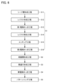
- FIG. 6 is a process diagram showing a method of manufacturing the coil device 100.
- the method of manufacturing the coil device 100 includes a printed wiring board forming step S1, a protective layer forming step S2, a through hole forming step S3, an electroless plating step S4, and a patterning step S5. have.
- the printed wiring board forming step S1 includes a seed layer forming step S11, a resist forming step S12, a first electrolytic plating step S13, a resist removing step S14, an etching step S15, and a second electrolytic plating step S16. ing.
- FIG. 7 is a cross-sectional view for explaining the seed layer forming step S11.
- the seed layer 15 first layer 15a, second layer 15b
- the first layer 15a is formed on the first major surface 11a and the second major surface 11b.
- the first layer 15a is formed by sputtering, for example.
- through holes 11c and 11d are formed.
- the through holes 11c and 11d are formed by, for example, irradiating laser light.
- the second layer 15b is formed on the first layer 15a. Although not shown, the second layer 15b is also formed on the inner wall surfaces of the through holes 11c and 11d.
- the second layer 15b is formed by, for example, electroless plating.
- FIG. 8 is a cross-sectional view for explaining the resist forming step S12.
- a resist 70 is formed in the resist forming step S12.
- the resist 70 is formed, for example, by applying a dry film resist onto the seed layer 15 and patterning the applied dry film resist by exposing and developing it.
- FIG. 9 is a cross-sectional view for explaining the first electroplating step S13.
- the first electroplating layer 16 is formed on the seed layer 15 exposed from the resist 70. As shown in FIG. although not shown, it is also formed on the second layer 15b on the inner wall surfaces of the through holes 11c and 11d.
- the first electrolytic plated layer 16 is formed by energizing the seed layer 15 in a plating solution containing the constituent material of the first electrolytic plated layer 16 .
- FIG. 10 is a cross-sectional view for explaining the resist removing step S14. As shown in FIG. 10, in the resist removing step S14, the resist 70 is removed by peeling.
- FIG. 11 is a cross-sectional view for explaining the etching step S15. As shown in FIG. 11, in the etching step S15, the seed layer 15 exposed between two adjacent portions of the first electroplating layer 16 is removed by etching.
- the second layer 15b is etched. Etching of the second layer 15b is performed by supplying an etchant between two adjacent portions of the first electroplating layer 16 .
- the etchant is selected so that etching is rate-determined by the reaction between the reactive species in the etchant and the object to be etched rather than the diffusion of the reactive species in the etchant to the vicinity of the object to be etched.
- the etchant used is an etchant that has a dissolution reaction rate of 1.0 ⁇ m/min or less for the material (that is, copper) forming the second layer 15b.
- the etching solution include sulfuric acid hydrogen peroxide aqueous solution and sodium peroxodisulfate aqueous solution. The dissolution reaction rate of the etchant is measured based on the weight of copper reduced after etching and the etching time.
- the first layer 15a is etched.
- the etchant is switched when the etching of the first layer 15a is performed.
- an etchant having a high selectivity with respect to the material (that is, nickel-chromium alloy) forming the first layer 15a is used. Therefore, after switching the etchant, the etching of the first electroplating layer 16 is difficult to proceed.
- FIG. 12 is a cross-sectional view for explaining the second electroplating step S16.
- the second electroplating layer 17 is formed so as to cover the seed layer 15 and the first electroplating layer 16.
- the second electrolytic plated layer 17 is also formed on the first electrolytic plated layer 16 on the inner wall surfaces of the through holes 11c and 11d with the second layer 15b interposed therebetween.
- the conductive layers 11e and 11f are composed of the second layer 15b, the first electrolytic plated layer 16 and the second electrolytic plated layer 17. As shown in FIG.
- the second electroplating layer 17 is formed by energizing the seed layer 15 and the first electroplating layer 16 in the plating solution containing the constituent materials of the second electroplating layer 17 .
- the printed wiring board 10 is formed using the semi-additive method.
- FIG. 13 is a cross-sectional view for explaining the protective layer forming step S2.
- the first protective layer 20 is formed on the first main surface 11a
- the second protective layer 30 is formed on the second main surface 11b.
- the base film 22 coated with the adhesive layer 21 is arranged on the first main surface 11a so as to cover the first coil wiring 12, and the adhesive layer 31 is applied.
- a base film 32 is arranged on the second main surface 11 b so as to cover the second coil wiring 13 .
- the adhesive layer 21 and the adhesive layer 31 are uncured.
- the base film 22 and the base film 32 are pressed toward the base film 11 while being heated. Thereby, the adhesive layer 21 and the adhesive layer 31 are cured, and the base film 22 and the base film 32 are attached.
- the copper layer 23 is arranged on the base film 22 and the copper layer 33 is arranged on the base film 32 when the protective layer forming step S2 is performed.
- FIG. 14 is a cross-sectional view explaining the through-hole forming step S3.
- through holes 20a are formed in the first protective layer 20 in the through hole forming step S3.
- the through hole 20a is formed by, for example, irradiating laser light.
- the through hole 20b is also formed in the same manner.
- FIG. 15 is a cross-sectional view explaining the electroless plating step S4.
- an electroless plated layer 24 is formed on the copper layer 23, and an electroless plated layer 34 is formed on the copper layer 33.
- the electroless plated layer 24 and the electroless plated layer 34 contain the constituent materials of the electroless plated layer 24 and the electroless plated layer 34 of the printed wiring board 10 on which the first protective layer 20 and the second protective layer 30 are formed. It is performed by immersion in a plating solution.
- the external connection terminals 40 and the conductive layer 50 are formed by patterning the copper layer 23 and the electroless plated layer 24 .
- the external connection terminals 41 and the conductive layer 51 are also formed along with the patterning of the copper layer 23 and the electroless plated layer 24 .
- Patterning of the copper layer 23 and the electroless plated layer 24 is performed by applying, for example, a dry film resist on the electroless plated layer 24, exposing and developing the applied dry film resist to form a resist, and masking the resist. This is carried out by etching the copper layer 23 and the electroless plated layer 24 as a layer. Since no resist is formed on the electroless plated layer 34, the copper layer 33 and the electroless plated layer 34 are all removed by the above etching. As described above, the coil device 100 having the structure shown in FIG. 1 is formed.
- the external connection terminals 40 and the external connection terminals 41 it is conceivable to arrange the external connection terminals 40 and the external connection terminals 41 on the first main surface 11a.
- the external connection terminals 40 and 41 are arranged on the first main surface 11a, the area of the first main surface 11a on which the first coil wiring 12 can be arranged is reduced. As a result, the area ratio of the first coil becomes smaller than the area ratio of the second coil.
- the area of the first main surface 11a on which the first coil wiring 12 can be arranged is It never decreases. Therefore, in the coil device 100, the area ratio of the first coil can be made approximately the same as the area ratio of the second coil, and the thrust of the coil device 100 can be increased.
- an etchant with a high dissolution reaction rate for the material forming the seed layer that is, an etchant in which the diffusion of the reactive species in the etchant to the vicinity of the etching target determines the etching rate
- an etchant with a high dissolution reaction rate for the material forming the seed layer that is, an etchant in which the diffusion of the reactive species in the etchant to the vicinity of the etching target determines the etching rate
- the etching in the etching step S15 is rate-determined by the reaction between the reactive species in the etching solution and the object to be etched, and the etching solution is supplied between two adjacent portions of the first electroplating layer 16. Even if it is difficult to etch the second layer 15b, variations in etching are unlikely to occur.
- the distance between two adjacent portions of the first coil wiring 12 (second coil wiring 13) can be shortened, and the first coil wiring 12 (second coil wiring 13) can be shortened. 13) can be increased in thickness.
- the area ratio of the first coil and the area ratio of the second coil can be increased, and the thrust of the coil device 100 can be increased.
- the width of the first coil wiring 12 (second coil wiring 13) can be increased. can. Therefore, according to the printed wiring board 10, the thickness and width of the first coil wiring 12 (second coil wiring 13) can be increased, and the electrical resistance value of the first coil wiring 12 (second coil wiring 13) can be increased to become smaller. As a result, it is possible to suppress an increase in the electrical resistance value accompanying an increase in the area ratio of the first coil and the area ratio of the second coil.
Landscapes
- Engineering & Computer Science (AREA)
- Power Engineering (AREA)
- Microelectronics & Electronic Packaging (AREA)
- Coils Or Transformers For Communication (AREA)
Abstract
This coil device has a first face and a second face as end faces in the thickness direction of the coil device. The coil device comprises at least one printed wiring board, a first protective layer, and an external connection terminal. The at least one printed wiring board comprises a first base film including a first principal surface and a second principal surface opposite to the first principal surface, a first coil wire spirally formed on the first principal surface, and a second coil wire spirally formed on the second principal surface. The first protective layer covers one first principal surface of the at least one printed wiring board closest to the first face. The external connection terminal is formed on the first protective layer and is electrically connected to the first coil wire.
Description
本開示は、コイル装置及びプリント配線板に関する。本出願は、2022年1月5日に出願した日本特許出願である特願2022-509号に基づく優先権及び2022年2月14日に出願した日本特許出願である特願2022-020717号に基づく優先権を主張する。当該日本特許出願に記載された全ての記載内容は、参照によって本明細書に援用される。
The present disclosure relates to a coil device and a printed wiring board. This application has priority based on Japanese Patent Application No. 2022-509 filed on January 5, 2022 and Japanese Patent Application No. 2022-020717 filed on February 14, 2022. claim priority under All the contents described in the Japanese patent application are incorporated herein by reference.
例えば特開2016-9854号公報(特許文献1)には、プリント配線板が記載されている。特許文献1に記載のプリント配線板は、ベースフィルムと配線とを有している。ベースフィルムは、第1主面と、第1主面の反対面である第2主面とを有している。配線は、第1主面上に配置されている第1配線と、第2主面上に配置されている第2配線とを有している。第1配線及び第2配線は、ベースフィルムに形成されているスルーホールの内壁面上に配置されているめっき層を介して互いに電気的に接続されている。第1配線及び第2配線は、渦巻状に巻回されていることにより、コイルを構成している。
For example, Japanese Patent Application Laid-Open No. 2016-9854 (Patent Document 1) describes a printed wiring board. The printed wiring board described in Patent Document 1 has a base film and wiring. The base film has a first major surface and a second major surface opposite to the first major surface. The wiring has a first wiring arranged on the first main surface and a second wiring arranged on the second main surface. The first wiring and the second wiring are electrically connected to each other via a plating layer arranged on the inner wall surface of the through hole formed in the base film. The first wiring and the second wiring constitute a coil by being spirally wound.
本開示のコイル装置は、コイル装置の厚さ方向における端面である第1面及び第2面を有する。コイル装置は、少なくとも1つのプリント配線板と、第1保護層と、外部接続端子とを備える。少なくとも1つのプリント配線板の各々は、第1主面及び第1主面の反対面である第2主面を含む第1ベースフィルムと、第1主面上に渦巻状に形成されている第1コイル配線と、第2主面上に渦巻状に形成されている第2コイル配線とを有する。第1保護層は、最も第1面の近くに配置されている少なくとも1つのプリント配線板のうちの1つの第1主面を覆っている。外部接続端子は、第1保護層上に形成されており、かつ第1コイル配線に電気的に接続されている。
The coil device of the present disclosure has a first surface and a second surface, which are end surfaces in the thickness direction of the coil device. The coil device includes at least one printed wiring board, a first protective layer, and external connection terminals. Each of the at least one printed wiring board includes a first base film including a first main surface and a second main surface opposite to the first main surface, and a second base film spirally formed on the first main surface. It has 1 coil wiring and the 2nd coil wiring formed spirally on the 2nd main surface. The first protective layer covers the first main surface of one of the at least one printed wiring board that is arranged closest to the first surface. The external connection terminal is formed on the first protective layer and electrically connected to the first coil wiring.
[本開示が解決しようとする課題]
特許文献1に記載のプリント配線板では、配線に接続されている外部接続端子を第1主面又は第2主面上に配置することが考えられる。しかしながら、この場合には、第1主面上の第1配線を配置できる面積又は第2主面上の第2配線を配置できる面積が減少してしまい、配線により構成されているコイルの推力が減少してしまうことになる。 [Problems to be Solved by the Present Disclosure]
In the printed wiring board described in Patent Document 1, it is conceivable to dispose the external connection terminals connected to the wiring on the first main surface or the second main surface. However, in this case, the area for arranging the first wiring on the first main surface or the area for arranging the second wiring on the second main surface is reduced, and the thrust of the coil formed by the wiring is reduced. will decrease.
本開示は、上記のような従来技術の問題点に鑑みてなされたものである。より具体的には、本開示は、推力の改善が可能なコイル装置を提供するものである。
The present disclosure has been made in view of the problems of the prior art as described above. More specifically, the present disclosure provides a coil system capable of improved thrust.
[本開示の効果]
本開示のコイル装置によると、推力の改善が可能である。 [Effect of the present disclosure]
According to the coil arrangement of the present disclosure, improved thrust is possible.
本開示のコイル装置によると、推力の改善が可能である。 [Effect of the present disclosure]
According to the coil arrangement of the present disclosure, improved thrust is possible.
[本開示の実施形態の説明]
まず、本開示の実施形態を列記して説明する。 [Description of Embodiments of the Present Disclosure]
First, embodiments of the present disclosure will be listed and described.
まず、本開示の実施形態を列記して説明する。 [Description of Embodiments of the Present Disclosure]
First, embodiments of the present disclosure will be listed and described.
(1)一実施形態に係るコイル装置は、コイル装置の厚さ方向における端面である第1面及び第2面を有する。コイル装置は、少なくとも1つのプリント配線板と、第1保護層と、外部接続端子とを備える。少なくとも1つのプリント配線板の各々は、第1主面及び第1主面の反対面である第2主面を含む第1ベースフィルムと、第1主面上に渦巻状に形成されている第1コイル配線と、第2主面上に渦巻状に形成されている第2コイル配線とを有する。第1保護層は、最も第1面の近くに配置されている少なくとも1つのプリント配線板のうちの1つの第1主面を覆っている。外部接続端子は、第1保護層上に形成されており、かつ第1コイル配線に電気的に接続されている。
(1) A coil device according to an embodiment has a first surface and a second surface, which are end surfaces in the thickness direction of the coil device. The coil device includes at least one printed wiring board, a first protective layer, and external connection terminals. Each of the at least one printed wiring board includes a first base film including a first main surface and a second main surface opposite to the first main surface, and a second base film spirally formed on the first main surface. It has 1 coil wiring and the 2nd coil wiring formed spirally on the 2nd main surface. The first protective layer covers the first main surface of one of the at least one printed wiring board that is arranged closest to the first surface. The external connection terminal is formed on the first protective layer and electrically connected to the first coil wiring.
(1)のコイル装置によると、推力の改善が可能である。
(2)(1)のコイル装置は、さらに、最も第1面の近くに配置されている少なくとも1つのプリント配線板のうちの1つの第1コイル配線と外部接続端子とを電気的に接続している導電層を備えていてもよい。第1保護層には、第1保護層を貫通している貫通穴が形成されていてもよい。貫通穴は、最も第1面の近くに配置されている少なくとも1つのプリント配線板のうちの1つの第1コイル配線を部分的に露出させていてもよい。導電層は、貫通穴から露出している第1コイル配線上及び貫通穴の内壁面上に形成されていてもよい。 According to the coil device of (1), thrust can be improved.
(2) The coil device of (1) further electrically connects the first coil wiring of one of the at least one printed wiring board arranged closest to the first surface and the external connection terminal. A conductive layer may be provided. A through hole penetrating through the first protective layer may be formed in the first protective layer. The through-hole may partially expose one first coil wire of the at least one printed wiring board arranged closest to the first surface. The conductive layer may be formed on the first coil wiring exposed from the through hole and on the inner wall surface of the through hole.
(3)(1)又は(2)のコイル装置は、さらに、少なくとも1つの第1接着層を備えていてもよい。少なくとも1つのプリント配線板は、複数のプリント配線板であってもよい。少なくとも1つの第1接着層は、複数のプリント配線板のうちの隣り合っている2つの間に配置されていてもよい。
(3) The coil device of (1) or (2) may further comprise at least one first adhesive layer. The at least one printed wiring board may be a plurality of printed wiring boards. At least one first adhesive layer may be disposed between two adjacent ones of the plurality of printed wiring boards.
(4)(3)のコイル装置では、複数のプリント配線板の数が、2つ又は3つであってもよい。
(4) In the coil device of (3), the number of printed wiring boards may be two or three.
(5)(1)から(4)のコイル装置では、第1保護層が、最も第1面の近くに配置されている少なくとも1つのプリント配線板のうちの1つの第1主面を覆っている第2接着層と、第2接着層上に配置されている第2ベースフィルムとを有していてもよい。
(5) In the coil devices of (1) to (4), the first protective layer covers the first major surface of one of the at least one printed wiring board located closest to the first surface. and a second base film disposed on the second adhesive layer.
(6)(1)から(5)のコイル装置は、第2保護層をさらに備えていてもよい。第2保護層は、最も第2面の近くに配置されている少なくとも1つのプリント配線板のうちの1つの第2主面を覆っていてもよい。
(6) The coil devices of (1) to (5) may further include a second protective layer. The second protective layer may cover the second major surface of one of the at least one printed wiring board located closest to the second surface.
(7)(6)のコイル装置では、第2保護層が、最も第2面の近くに配置されている少なくとも1つのプリント配線板のうちの1つの第2主面を覆っている第3接着層と、第3接着層上に配置されている第3ベースフィルムとを有していてもよい。
(7) In the coil device of (6), the second protective layer covers the second major surface of one of the at least one printed wiring board located closest to the second surface. and a third base film disposed on the third adhesive layer.
(8)(6)又は(7)のコイル装置では、第1保護層の厚さが、5μm以上50μm以下であり、かつ第2保護層の厚さの0.8倍以上1.2倍以下であってもよい。
(8) In the coil device of (6) or (7), the thickness of the first protective layer is 5 µm or more and 50 µm or less, and 0.8 times or more and 1.2 times or less of the thickness of the second protective layer. may be
(9)(1)から(8)のコイル装置では、第1コイル配線により構成されているコイルの面積を第1主面の面積で除した値及び第2コイル配線により構成されているコイルの面積を第2主面の面積で除した値の少なくともいずれかが、0.40以上0.90以下であってもよい。
(9) In the coil devices of (1) to (8), the value obtained by dividing the area of the coil configured by the first coil wiring by the area of the first main surface and the area of the coil configured by the second coil wiring At least one of the values obtained by dividing the area by the area of the second main surface may be 0.40 or more and 0.90 or less.
(10)(1)から(9)のコイル装置では、第1コイル配線により構成されているコイルの面積を第1主面の面積で除した値及び第2コイル配線により構成されているコイルの面積を第2主面の面積で除した値の少なくともいずれかが、0.60以上0.90以下であってもよい。
(10) In the coil devices of (1) to (9), the value obtained by dividing the area of the coil configured by the first coil wiring by the area of the first main surface and the area of the coil configured by the second coil wiring At least one of the values obtained by dividing the area by the area of the second main surface may be 0.60 or more and 0.90 or less.
(11)(1)から(10)のコイル装置では、第1コイル配線の幅及び第2コイル配線の幅が20μm以上40μm以下であってもよい。第1コイル配線の厚さ及び第2コイル配線の厚さは30μm以上70μm以下であってもよい。隣り合っている第1コイル配線の2つの部分の間の距離及び隣り合っている第2コイル配線の2つの部分の間の距離は3μm以上15μm以下であってもよい。
(11) In the coil devices of (1) to (10), the width of the first coil wiring and the width of the second coil wiring may be 20 μm or more and 40 μm or less. The thickness of the first coil wiring and the thickness of the second coil wiring may be 30 μm or more and 70 μm or less. A distance between two adjacent portions of the first coil wiring and a distance between two adjacent portions of the second coil wiring may be 3 μm or more and 15 μm or less.
(12)(1)から(11)のコイル装置では、第1コイル配線により構成されているコイルの面積を第1主面の面積で除した値が、第2コイル配線により構成されているコイルの面積を第2主面の面積で除した値の0.95倍以上1.05倍以下であってもよい。
(12) In the coil device of (1) to (11), the value obtained by dividing the area of the coil configured by the first coil wiring by the area of the first main surface is the coil configured by the second coil wiring. 0.95 times or more and 1.05 times or less of the value obtained by dividing the area of by the area of the second main surface.
(13)一実施形態に係るプリント配線板は、第1主面及び第1主面の反対面である第2主面を有する第1ベースフィルムと、第1主面上に渦巻状に形成されている第1コイル配線と、第2主面上に渦巻状に形成されている第2コイル配線とを備える。第1コイル配線により構成されているコイルの面積を第1主面の面積で除した値及び第2コイル配線により構成されているコイルの面積を第2主面の面積で除した値の少なくともいずれかは、0.40以上0.90以下である。
(13) A printed wiring board according to one embodiment includes a first base film having a first main surface and a second main surface opposite to the first main surface, and a spirally formed base film on the first main surface. and a second coil wiring spirally formed on the second main surface. At least one of a value obtained by dividing the area of the coil formed by the first coil wiring by the area of the first main surface and a value obtained by dividing the area of the coil formed by the second coil wiring by the area of the second main surface is between 0.40 and 0.90.
(13)のプリント配線板によると、コイル装置に用いた際に、推力の改善が可能である。
According to the printed wiring board (13), it is possible to improve thrust when used in a coil device.
(14)(13)のプリント配線板では、第1コイル配線により構成されているコイルの面積を第1主面の面積で除した値及び第2コイル配線により構成されているコイルの面積を第2主面の面積で除した値の少なくともいずれかが、0.60以上0.90であってもよい。
(14) In the printed wiring board of (13), the value obtained by dividing the area of the coil formed by the first coil wiring by the area of the first main surface and the area of the coil formed by the second coil wiring are the At least one of the values divided by the areas of the two main surfaces may be 0.60 or more and 0.90.
(15)(13)又は(14)のプリント配線板では、第1コイル配線により構成されているコイルの面積を第1主面の面積で除した値が、第2コイル配線により構成されているコイルの面積を第2主面の面積で除した値の0.95倍以上1.05倍以下であってもよい。
(15) In the printed wiring board of (13) or (14), the value obtained by dividing the area of the coil formed by the first coil wiring by the area of the first main surface is formed by the second coil wiring. It may be 0.95 to 1.05 times the value obtained by dividing the area of the coil by the area of the second main surface.
(16)他の実施形態に係るプリント配線板は、第1主面及び第1主面の反対面である第2主面を有する第1ベースフィルムと、第1主面上に渦巻状に形成されている第1コイル配線と、第2主面上に渦巻状に形成されている第2コイル配線とを備える。第1コイル配線の幅を隣り合っている第1コイル配線の2つの部分の間のピッチで除した値及び第2コイル配線の幅を隣り合っている第2コイル配線の2つの部分の間のピッチで除した値は0.72以上0.93以下である。
(16) A printed wiring board according to another embodiment includes a first base film having a first main surface and a second main surface opposite to the first main surface, and a base film spirally formed on the first main surface. and a second coil wiring spirally formed on the second main surface. The value obtained by dividing the width of the first coil wiring by the pitch between two portions of the adjacent first coil wiring and the width of the second coil wiring between the two portions of the adjacent second coil wiring The value divided by the pitch is 0.72 or more and 0.93 or less.
(16)のプリント配線板によると、コイル装置に用いた際に、推力の改善が可能である。
According to the printed wiring board (16), it is possible to improve thrust when used in a coil device.
[本開示の実施形態の詳細]
次に、本開示の実施形態の詳細を、図面を参照しながら説明する。以下の図面では、同一又は相当する部分に同一の参照符号を付し、重複する説明は繰り返さないものとする。 [Details of the embodiment of the present disclosure]
Next, details of embodiments of the present disclosure will be described with reference to the drawings. In the drawings below, the same or corresponding parts are denoted by the same reference numerals, and redundant description will not be repeated.
(実施形態に係るコイル装置の構成)
以下に、実施形態に係るコイル装置の構成を説明する。実施形態に係るコイル装置を、コイル装置100とする。 (Configuration of coil device according to embodiment)
The configuration of the coil device according to the embodiment will be described below. A coil device according to the embodiment is referred to as acoil device 100 .
以下に、実施形態に係るコイル装置の構成を説明する。実施形態に係るコイル装置を、コイル装置100とする。 (Configuration of coil device according to embodiment)
The configuration of the coil device according to the embodiment will be described below. A coil device according to the embodiment is referred to as a
図1は、コイル装置100の断面図である。図2は、プリント配線板10の平面図である。図3は、プリント配線板10の底面図である。図3には、図2とは反対側から見たプリント配線板10が示されている。図1、図2及び図3に示されるように、コイル装置100は、プリント配線板10と、第1保護層20と、第2保護層30と、外部接続端子40と、導電層50とを有している。コイル装置100は、第1面100aと、第2面100bとを有している。第1面100a及び第2面100bは、厚さ方向におけるコイル装置100の端面である。第2面100bは、第1面100aの反対面である。
FIG. 1 is a cross-sectional view of the coil device 100. FIG. FIG. 2 is a plan view of the printed wiring board 10. FIG. FIG. 3 is a bottom view of the printed wiring board 10. FIG. FIG. 3 shows printed wiring board 10 viewed from the opposite side to FIG. As shown in FIGS. 1, 2 and 3, the coil device 100 includes a printed wiring board 10, a first protective layer 20, a second protective layer 30, external connection terminals 40, and a conductive layer 50. have. The coil device 100 has a first surface 100a and a second surface 100b. The first surface 100a and the second surface 100b are end surfaces of the coil device 100 in the thickness direction. The second surface 100b is the opposite surface of the first surface 100a.
プリント配線板10は、ベースフィルム11と、第1コイル配線12と、第2コイル配線13と、接続配線14とを有している。
The printed wiring board 10 has a base film 11 , a first coil wiring 12 , a second coil wiring 13 and a connection wiring 14 .
ベースフィルム11は、第1主面11aと、第2主面11bとを有している。第1主面11a及び第2主面11bは、厚さ方向におけるベースフィルム11の端面である。ベースフィルム11は、可撓性のある電気絶縁性の材料により形成されている。ベースフィルム11は、例えば、ポリイミド、ポリエチレンテレフタレート又はフッ素樹脂により形成されている。
The base film 11 has a first main surface 11a and a second main surface 11b. The first main surface 11a and the second main surface 11b are end surfaces of the base film 11 in the thickness direction. The base film 11 is made of a flexible, electrically insulating material. The base film 11 is made of, for example, polyimide, polyethylene terephthalate, or fluororesin.
第1コイル配線12は、第1主面11a上に配置されている。第1コイル配線12は、平面視において、渦巻状に巻回されている。第2コイル配線13は、第2主面11b上に配置されている。第2コイル配線13は、平面視において、渦巻状に巻回されている。接続配線14は、第1主面11a上に配置されている。
The first coil wiring 12 is arranged on the first main surface 11a. The first coil wiring 12 is spirally wound in plan view. The second coil wiring 13 is arranged on the second main surface 11b. The second coil wiring 13 is spirally wound in plan view. The connection wiring 14 is arranged on the first main surface 11a.
第1コイル配線12の一方端及び他方端は、それぞれランド12a及びランド12bになっている。第2コイル配線13の一方端は、それぞれランド13a及びランド13bになっている。接続配線14の一方端及び他方端は、それぞれランド14a及びランド14bになっている。ランド12b及びランド13aは、平面視において、互いに重なっている。ランド13b及びランド14aは、平面視において、互いに重なっている。
One end and the other end of the first coil wiring 12 are lands 12a and 12b, respectively. One ends of the second coil wiring 13 are lands 13a and 13b, respectively. One end and the other end of the connection wiring 14 are lands 14a and 14b, respectively. The land 12b and the land 13a overlap each other in plan view. The land 13b and the land 14a overlap each other in plan view.
ベースフィルム11には、厚さ方向に沿ってベースフィルム11を貫通している貫通穴11c(図示せず)及び貫通穴11d(図示せず)が形成されている。貫通穴11cは、平面視においてランド12b及びランド13aと重なっている。貫通穴11dは、平面視においてランド13b及びランド14aと重なっている。第1コイル配線12及び第2コイル配線13は、貫通穴11cの内壁面上に形成されている導電層11e(図示せず)により互いに電気的に接続されている。第2コイル配線13及び接続配線14は、貫通穴11dの内壁面上に形成されている導電層11f(図示せず)により互いに電気的に接続されている。
The base film 11 is formed with a through hole 11c (not shown) and a through hole 11d (not shown) penetrating the base film 11 along the thickness direction. The through hole 11c overlaps the land 12b and the land 13a in plan view. The through hole 11d overlaps the land 13b and the land 14a in plan view. The first coil wiring 12 and the second coil wiring 13 are electrically connected to each other by a conductive layer 11e (not shown) formed on the inner wall surface of the through hole 11c. The second coil wire 13 and the connection wire 14 are electrically connected to each other by a conductive layer 11f (not shown) formed on the inner wall surface of the through hole 11d.
第1コイル配線12及び第2コイル配線13の各々は、シード層15と、第1電解めっき層16と、第2電解めっき層17とを有している。
Each of the first coil wiring 12 and the second coil wiring 13 has a seed layer 15 , a first electroplating layer 16 and a second electroplating layer 17 .
シード層15は、ベースフィルム11の主面(第1主面11a、第2主面11b)上に配置されている。シード層15は、第1層15aと、第2層15bとを有している。第1層15aは、ベースフィルム11の主面(第1主面11a、第2主面11b)上に配置されている。第2層15bは、第1層15a上に配置されている。
The seed layer 15 is arranged on the main surfaces of the base film 11 (the first main surface 11a and the second main surface 11b). The seed layer 15 has a first layer 15a and a second layer 15b. The first layer 15a is arranged on the main surfaces (first main surface 11a, second main surface 11b) of the base film 11 . The second layer 15b is arranged on the first layer 15a.
第1層15aは、例えば、ニッケル-クロム合金により形成されているスパッタ層(スパッタリングにより形成されている層)である。第2層15bは、例えば銅により形成されている無電解めっき層(無電解めっきにより形成されている層)である。
The first layer 15a is, for example, a sputtered layer (a layer formed by sputtering) made of a nickel-chromium alloy. The second layer 15b is an electroless plated layer (layer formed by electroless plating) made of copper, for example.
第1電解めっき層16はシード層15上に配置されている。第1電解めっき層16は、銅により形成されている電解めっき層である。第2電解めっき層17は、シード層15及び第1電解めっき層16を覆っている。より具体的には、第2電解めっき層17は、シード層15の側面上並びに第1電解めっき層16の側面上及び上面上に配置されている。
The first electroplating layer 16 is arranged on the seed layer 15 . The first electrolytic plated layer 16 is an electrolytic plated layer made of copper. The second electroplating layer 17 covers the seed layer 15 and the first electroplating layer 16 . More specifically, the second electrolytic plated layer 17 is arranged on the side surfaces of the seed layer 15 and on the side surfaces and the upper surface of the first electrolytic plated layer 16 .
第1コイル配線12により構成されているコイルを、第1コイルとする。第2コイル配線13により構成されているコイルを、第2コイルとする。第1コイルの面積割合及び第2コイルの面積割合の少なくともいずれかは、0.40以上0.90以下であることが好ましい。第1コイルの面積割合及び第2コイルの面積割合の少なくともいずれかは、0.60以上0.90以下であることがさらに好ましい。第1コイルの面積割合は、第2コイルの面積割合の0.95倍以上1.05倍以下であることが好ましい。
A coil configured by the first coil wiring 12 is referred to as a first coil. A coil configured by the second coil wiring 13 is referred to as a second coil. At least one of the area ratio of the first coil and the area ratio of the second coil is preferably 0.40 or more and 0.90 or less. At least one of the area ratio of the first coil and the area ratio of the second coil is more preferably 0.60 or more and 0.90 or less. The area ratio of the first coil is preferably 0.95 to 1.05 times the area ratio of the second coil.
第1コイルの面積割合は第1コイルの面積を第1主面11aの面積で除した値であり、第2コイルの面積割合は第2コイルの面積を第2主面11bの面積で除した値である。第1コイルの面積は、第1コイル配線12の面積と隣り合っている第1コイル配線12の2つの部分の間にある第1主面11aの面積との和である。第2コイルの面積は、第2コイル配線13の面積と隣り合っている第2コイル配線13の2つの部分の間にある第2主面11bの面積との和である。
The area ratio of the first coil is a value obtained by dividing the area of the first coil by the area of the first main surface 11a, and the area ratio of the second coil is obtained by dividing the area of the second coil by the area of the second main surface 11b. value. The area of the first coil is the sum of the area of the first coil wire 12 and the area of the first main surface 11a between two portions of the first coil wire 12 adjacent to each other. The area of the second coil is the sum of the area of the second coil wire 13 and the area of the second main surface 11b between two portions of the second coil wire 13 adjacent to each other.
第1コイル配線12の面積は、第1主面11a側から見た平面視における第1コイル配線12の面積である。すなわち、第1コイル配線12の面積には第1コイル配線12の側面の面積は含まれない。第2コイル配線13の面積は、第2主面11b側から見た平面視における第2コイル配線13の面積である。すなわち、第2コイル配線13の面積には、第2コイル配線13の側面の面積は含まれない。
The area of the first coil wiring 12 is the area of the first coil wiring 12 in plan view from the first main surface 11a side. That is, the area of the first coil wiring 12 does not include the side surface area of the first coil wiring 12 . The area of the second coil wiring 13 is the area of the second coil wiring 13 in a plan view seen from the second main surface 11b side. That is, the area of the second coil wiring 13 does not include the side surface area of the second coil wiring 13 .
図4は、第1コイルの面積を説明するプリント配線板10の平面図である。図4に示されるように、隣り合っている第1コイル配線12の2つの部分の間以外にある第1主面11aの面積(図4中のクロスハッチング部分)は、第1コイルの面積には含まれない。図示されていないが、隣り合っている第2コイル配線13の2つの部分の間以外にある第2主面11bも、同様に、第2コイルの面積に含まれない。
FIG. 4 is a plan view of the printed wiring board 10 explaining the area of the first coil. As shown in FIG. 4, the area of the first main surface 11a (cross-hatched portion in FIG. 4) other than between two portions of the adjacent first coil wiring 12 is the area of the first coil. is not included. Although not shown, the second main surface 11b other than between two portions of the second coil wiring 13 adjacent to each other is also not included in the area of the second coil.
第1コイル配線12の幅を幅W1とし、第2コイル配線13の幅を幅W2とする。幅W1及び幅W2は、20μm以上40μm以下であることが好ましい。第1コイル配線12の厚さを、厚さT1とする。第2コイル配線13の厚さを、厚さT2とする。厚さT1及び厚さT2は、30μm以上70μm以下であることが好ましい。第1コイル配線12の隣り合っている2つの部分の間の距離を、距離L1とする。第2コイル配線13の隣り合っている2つの部分の間の距離を、距離L2とする。距離L1及び距離L2は、3μm以上15μm以下であることが好ましい。
The width of the first coil wiring 12 is assumed to be W1, and the width of the second coil wiring 13 is assumed to be W2. The width W1 and the width W2 are preferably 20 μm or more and 40 μm or less. The thickness of the first coil wiring 12 is assumed to be thickness T1. The thickness of the second coil wiring 13 is assumed to be thickness T2. The thickness T1 and the thickness T2 are preferably 30 μm or more and 70 μm or less. A distance between two adjacent portions of the first coil wiring 12 is defined as a distance L1. A distance between two adjacent portions of the second coil wiring 13 is defined as a distance L2. The distance L1 and the distance L2 are preferably 3 μm or more and 15 μm or less.
第1コイル配線12の隣り合っている2つの部分の間のピッチを、ピッチP1とする。第2コイル配線13の隣り合っている2つの部分の間のピッチを、ピッチP2とする。幅W1をピッチP1で除した値及び幅W2をピッチP2で除した値は、0.72以上0.93以下であることが好ましい。
The pitch between two adjacent portions of the first coil wiring 12 is defined as a pitch P1. A pitch between two adjacent portions of the second coil wiring 13 is defined as a pitch P2. The value obtained by dividing the width W1 by the pitch P1 and the value obtained by dividing the width W2 by the pitch P2 are preferably 0.72 or more and 0.93 or less.
第1保護層20は、第1主面11aを覆っている。第1保護層20は、接着層21と、ベースフィルム22とを有している。接着層21は、第1主面11aを覆っている。ベースフィルム22は、接着層21上に配置されている。接着層21は、例えば接着剤により形成されている。ベースフィルム22は、例えばポリイミド、ポリエチレンテレフタレート又はフッ素樹脂により形成されている。
The first protective layer 20 covers the first main surface 11a. The first protective layer 20 has an adhesive layer 21 and a base film 22 . The adhesive layer 21 covers the first main surface 11a. A base film 22 is arranged on the adhesive layer 21 . The adhesive layer 21 is made of, for example, an adhesive. The base film 22 is made of polyimide, polyethylene terephthalate, or fluorine resin, for example.
第1保護層20には、貫通穴20aが形成されている。貫通穴20aは、厚さ方向に沿って第1保護層20を貫通し、第1コイル配線12を部分的に露出させている。貫通穴20aからは、例えばランド12aが露出している。第1保護層20の厚さを、厚さT3とする。厚さT3は、第1コイル配線12の上面と第1保護層20の表面との間の距離である。厚さT3は、5μm以上50μm以下であることが好ましい。
A through hole 20 a is formed in the first protective layer 20 . The through hole 20a penetrates the first protective layer 20 along the thickness direction and partially exposes the first coil wiring 12 . For example, the land 12a is exposed from the through hole 20a. The thickness of the first protective layer 20 is assumed to be thickness T3. The thickness T3 is the distance between the top surface of the first coil wire 12 and the surface of the first protective layer 20 . The thickness T3 is preferably 5 μm or more and 50 μm or less.
第2保護層30は、第2主面11bを覆っている。第2保護層30は、接着層31と、ベースフィルム32とを有している。接着層31は、第2主面11bを覆っている。ベースフィルム32は、接着層31上に配置されている。接着層31は、例えば接着剤により形成されている。ベースフィルム32は、例えばポリイミド、ポリエチレンテレフタレート又はフッ素樹脂により形成されている。
The second protective layer 30 covers the second main surface 11b. The second protective layer 30 has an adhesive layer 31 and a base film 32 . The adhesive layer 31 covers the second main surface 11b. A base film 32 is arranged on the adhesive layer 31 . The adhesive layer 31 is made of, for example, an adhesive. The base film 32 is made of polyimide, polyethylene terephthalate, or fluorine resin, for example.
第2保護層30の厚さを、厚さT4とする。厚さT4は、第2コイル配線13の上面と第2保護層30の表面との間の距離である。厚さT4は、5μm以上50μm以下であることが好ましい。厚さT3は、厚さT4の0.8倍以上1.2倍以下であることが好ましい。
The thickness of the second protective layer 30 is assumed to be thickness T4. The thickness T4 is the distance between the top surface of the second coil wire 13 and the surface of the second protective layer 30 . The thickness T4 is preferably 5 μm or more and 50 μm or less. The thickness T3 is preferably 0.8 to 1.2 times the thickness T4.
外部接続端子40は、第1保護層20(ベースフィルム22)上に配置されている。外部接続端子40は、例えば銅により形成されている。導電層50は、例えば、銅により形成されている無電解めっき層である。導電層50は、貫通穴20aから露出している第1コイル配線12の部分(例えば、ランド12a)上及び貫通穴20aの内壁面上に配置されている。また、導電層50は、外部接続端子40上にも配置されている。そのため、導電層50により、外部接続端子40と第1コイル配線12とが電気的に接続されている。
The external connection terminals 40 are arranged on the first protective layer 20 (base film 22). The external connection terminals 40 are made of copper, for example. The conductive layer 50 is an electroless plated layer made of copper, for example. The conductive layer 50 is arranged on the portion (for example, the land 12a) of the first coil wire 12 exposed from the through hole 20a and on the inner wall surface of the through hole 20a. The conductive layer 50 is also arranged on the external connection terminals 40 . Therefore, the conductive layer 50 electrically connects the external connection terminal 40 and the first coil wiring 12 .
図示されていないが、第1保護層20にはランド14bを露出させる貫通穴20aとは別の貫通穴20bが形成されており、第1保護層20上には外部接続端子40とは別の外部接続端子41が配置されている。また、貫通穴20bの内壁面上、ランド14b上及び外部接続端子41上に導電層50とは別の導電層51(図示せず)が配置されることにより、外部接続端子41は、接続配線14に電気的に接続されている。
Although not shown, through holes 20b are formed in the first protective layer 20 in addition to the through holes 20a for exposing the lands 14b. An external connection terminal 41 is arranged. Further, a conductive layer 51 (not shown) separate from the conductive layer 50 is arranged on the inner wall surface of the through hole 20b, on the land 14b, and on the external connection terminal 41, so that the external connection terminal 41 can be used as a connection wiring. 14 are electrically connected.
接続配線14は第2コイル配線13に電気的に接続されており、第2コイル配線13は第1コイル配線12に電気邸に接続されているため、外部接続端子40と外部接続端子41との間に電圧が印加されることにより、第1コイル配線12及び第2コイル配線13に電流が流れ、第1コイル及び第2コイルが磁場を発生させることになる。
The connection wiring 14 is electrically connected to the second coil wiring 13 , and the second coil wiring 13 is connected to the first coil wiring 12 to the electric house. By applying a voltage between them, a current flows through the first coil wiring 12 and the second coil wiring 13, and the first coil and the second coil generate a magnetic field.
<変形例>
図5は、変形例に係るコイル装置100の断面図である。図5に示されるように、コイル装置100は、複数のプリント配線板10を有していてもよい。プリント配線板10の数は、好ましくは2つ又は3つである。この場合、コイル装置100の厚さ方向において隣り合っている2つのプリント配線板10は、接着層60により互いに接着されている。また、この場合、第1保護層20は最も第1面100aの近くにあるプリント配線板10の第1主面11aを覆っており、第2保護層30は最も第2面100bの近くにあるプリント配線板10の第2主面11bを覆っている。 <Modification>
FIG. 5 is a cross-sectional view of acoil device 100 according to a modification. As shown in FIG. 5 , the coil device 100 may have multiple printed wiring boards 10 . The number of printed wiring boards 10 is preferably two or three. In this case, two printed wiring boards 10 that are adjacent in the thickness direction of coil device 100 are adhered to each other by adhesive layer 60 . Also, in this case, the first protective layer 20 covers the first main surface 11a of the printed wiring board 10 closest to the first surface 100a, and the second protective layer 30 is closest to the second surface 100b. It covers the second main surface 11 b of the printed wiring board 10 .
図5は、変形例に係るコイル装置100の断面図である。図5に示されるように、コイル装置100は、複数のプリント配線板10を有していてもよい。プリント配線板10の数は、好ましくは2つ又は3つである。この場合、コイル装置100の厚さ方向において隣り合っている2つのプリント配線板10は、接着層60により互いに接着されている。また、この場合、第1保護層20は最も第1面100aの近くにあるプリント配線板10の第1主面11aを覆っており、第2保護層30は最も第2面100bの近くにあるプリント配線板10の第2主面11bを覆っている。 <Modification>
FIG. 5 is a cross-sectional view of a
(実施形態に係るコイル装置の製造方法)
以下に、コイル装置100の製造方法を説明する。 (Manufacturing method of coil device according to embodiment)
A method of manufacturing thecoil device 100 will be described below.
以下に、コイル装置100の製造方法を説明する。 (Manufacturing method of coil device according to embodiment)
A method of manufacturing the
図6は、コイル装置100の製造方法を示す工程図である。図6に示されるように、コイル装置100の製造方法は、プリント配線板形成工程S1と、保護層形成工程S2と、貫通穴形成工程S3と、無電解めっき工程S4と、パターンニング工程S5とを有している。プリント配線板形成工程S1は、シード層形成工程S11と、レジスト形成工程S12と、第1電解めっき工程S13と、レジスト除去工程S14と、エッチング工程S15と、第2電解めっき工程S16とを有している。
FIG. 6 is a process diagram showing a method of manufacturing the coil device 100. FIG. As shown in FIG. 6, the method of manufacturing the coil device 100 includes a printed wiring board forming step S1, a protective layer forming step S2, a through hole forming step S3, an electroless plating step S4, and a patterning step S5. have. The printed wiring board forming step S1 includes a seed layer forming step S11, a resist forming step S12, a first electrolytic plating step S13, a resist removing step S14, an etching step S15, and a second electrolytic plating step S16. ing.
図7は、シード層形成工程S11を説明する断面図である。シード層形成工程S11では、シード層15(第1層15a、第2層15b)が形成される。シード層形成工程S11では、第1に、第1主面11a上及び第2主面11b上に第1層15aが形成される。第1層15aは、例えば、スパッタリングにより形成される。第2に、図示されていないが、貫通穴11c及び貫通穴11dが形成される。貫通穴11c及び貫通穴11dは、例えばレーザ光を照射することにより形成される。
FIG. 7 is a cross-sectional view for explaining the seed layer forming step S11. In the seed layer forming step S11, the seed layer 15 (first layer 15a, second layer 15b) is formed. In the seed layer forming step S11, first, the first layer 15a is formed on the first major surface 11a and the second major surface 11b. The first layer 15a is formed by sputtering, for example. Secondly, although not shown, through holes 11c and 11d are formed. The through holes 11c and 11d are formed by, for example, irradiating laser light.
第3に、第1層15a上に第2層15bが形成される。図示されていないが、第2層15bは、貫通穴11c及び貫通穴11dの内壁面上にも形成される。第2層15bの形成は、例えば、無電解めっきにより形成される。
Third, the second layer 15b is formed on the first layer 15a. Although not shown, the second layer 15b is also formed on the inner wall surfaces of the through holes 11c and 11d. The second layer 15b is formed by, for example, electroless plating.
図8は、レジスト形成工程S12を説明する断面図である。図8に示されるように、レジスト形成工程S12では、レジスト70が形成される。レジスト70は、例えば、シード層15上にドライフィルムレジストを貼付するとともに、貼付されたドライフィルムレジストを露光及び現像してパターンニングすることにより形成される。
FIG. 8 is a cross-sectional view for explaining the resist forming step S12. As shown in FIG. 8, a resist 70 is formed in the resist forming step S12. The resist 70 is formed, for example, by applying a dry film resist onto the seed layer 15 and patterning the applied dry film resist by exposing and developing it.
図9は、第1電解めっき工程S13を説明する断面図である。図9に示されるように、第1電解めっき工程S13では、レジスト70から露出しているシード層15上に第1電解めっき層16が形成される。図示されていないが、貫通穴11c及び貫通穴11dの内壁面上にある第2層15b上にも形成される。第1電解めっき層16は、第1電解めっき層16の構成材料が含まれているめっき液中においてシード層15に通電することにより形成される。
FIG. 9 is a cross-sectional view for explaining the first electroplating step S13. As shown in FIG. 9, in the first electroplating step S13, the first electroplating layer 16 is formed on the seed layer 15 exposed from the resist 70. As shown in FIG. Although not shown, it is also formed on the second layer 15b on the inner wall surfaces of the through holes 11c and 11d. The first electrolytic plated layer 16 is formed by energizing the seed layer 15 in a plating solution containing the constituent material of the first electrolytic plated layer 16 .
図10は、レジスト除去工程S14を説明する断面図である。図10に示されているように、レジスト除去工程S14では、レジスト70が剥離されることにより除去される。図11は、エッチング工程S15を説明する断面図である。図11に示されるように、エッチング工程S15では、第1電解めっき層16の隣り合っている2つの部分の間から露出しているシード層15が、エッチングにより除去される。
FIG. 10 is a cross-sectional view for explaining the resist removing step S14. As shown in FIG. 10, in the resist removing step S14, the resist 70 is removed by peeling. FIG. 11 is a cross-sectional view for explaining the etching step S15. As shown in FIG. 11, in the etching step S15, the seed layer 15 exposed between two adjacent portions of the first electroplating layer 16 is removed by etching.
エッチング工程S15では、第1に、第2層15bに対するエッチングが行われる。第2層15bに対するエッチングは、第1電解めっき層16の隣り合っている2つの部分の間にエッチング液を供給することにより行われる。エッチング液は、エッチング液中の反応種のエッチング対象近傍への拡散ではなくエッチング液中の反応種とエッチング対象との反応によりエッチングが律速されるように選択される。
In the etching step S15, first, the second layer 15b is etched. Etching of the second layer 15b is performed by supplying an etchant between two adjacent portions of the first electroplating layer 16 . The etchant is selected so that etching is rate-determined by the reaction between the reactive species in the etchant and the object to be etched rather than the diffusion of the reactive species in the etchant to the vicinity of the object to be etched.
より具体的には、エッチング液には、第2層15bを構成している材料(すなわち銅)に対する溶解反応速度が1.0μm/分以下となるエッチング液が用いられる。上記のエッチング液の具体例としては、硫酸過酸化水素水溶液又はペルオキソ二硫酸ナトリウム水溶液が挙げられる。なお、上記のエッチング液の溶解反応速度は、エッチング後に減少した銅の重量及びエッチング時間に基づいて測定される。
More specifically, the etchant used is an etchant that has a dissolution reaction rate of 1.0 μm/min or less for the material (that is, copper) forming the second layer 15b. Specific examples of the etching solution include sulfuric acid hydrogen peroxide aqueous solution and sodium peroxodisulfate aqueous solution. The dissolution reaction rate of the etchant is measured based on the weight of copper reduced after etching and the etching time.
エッチング工程S15では、第2に、第1層15aに対するエッチングが行われる。第1層15aのエッチングが行われる際に、エッチング液が切り換えられる。切り換え後のエッチング液には、第1層15aを構成している材料(すなわちニッケル-クロム合金)に対する選択比が高いエッチング液が用いられる。そのため、エッチング液の切り換え後には、第1電解めっき層16に対するエッチングは進行しにくい。
Secondly, in the etching step S15, the first layer 15a is etched. The etchant is switched when the etching of the first layer 15a is performed. As the etchant after switching, an etchant having a high selectivity with respect to the material (that is, nickel-chromium alloy) forming the first layer 15a is used. Therefore, after switching the etchant, the etching of the first electroplating layer 16 is difficult to proceed.
図12は、第2電解めっき工程S16を説明する断面図である。図12に示されるように、第2電解めっき工程S16では、シード層15及び第1電解めっき層16を覆うように第2電解めっき層17が形成される。なお、図示されていないが、第2層15bを介在させて貫通穴11c及び貫通穴11dの内壁面上にある第1電解めっき層16上にも、第2電解めっき層17が形成される。このことを別の観点から言えば、導電層11e及び導電層11fは、第2層15b、第1電解めっき層16及び第2電解めっき層17により構成されている。
FIG. 12 is a cross-sectional view for explaining the second electroplating step S16. As shown in FIG. 12, in the second electroplating step S16, the second electroplating layer 17 is formed so as to cover the seed layer 15 and the first electroplating layer 16. As shown in FIG. Although not shown, the second electrolytic plated layer 17 is also formed on the first electrolytic plated layer 16 on the inner wall surfaces of the through holes 11c and 11d with the second layer 15b interposed therebetween. From another point of view, the conductive layers 11e and 11f are composed of the second layer 15b, the first electrolytic plated layer 16 and the second electrolytic plated layer 17. As shown in FIG.
第2電解めっき層17は、第2電解めっき層17の構成材料含まれているめっき液中においてシード層15及び第1電解めっき層16に通電することにより形成される。以上により、プリント配線板10が、セミアディティブ工法を用いて形成される。
The second electroplating layer 17 is formed by energizing the seed layer 15 and the first electroplating layer 16 in the plating solution containing the constituent materials of the second electroplating layer 17 . As described above, the printed wiring board 10 is formed using the semi-additive method.
図13は、保護層形成工程S2を説明する断面図である。図13に示されるように、保護層形成工程S2では、第1主面11a上に第1保護層20が形成されるとともに、第2主面11b上に第2保護層30が形成される。保護層形成工程S2では、第1に、接着層21が塗布されているベースフィルム22が第1コイル配線12を覆うように第1主面11a上に配置されるとともに、接着層31が塗布されているベースフィルム32が第2コイル配線13を覆うように第2主面11b上に配置される。この段階で、接着層21及び接着層31は、未硬化である。第2に、加熱された状態で、ベースフィルム22及びベースフィルム32がベースフィルム11に向かって加圧される。これにより、接着層21及び接着層31が硬化され、ベースフィルム22及びベースフィルム32が貼付される。
FIG. 13 is a cross-sectional view for explaining the protective layer forming step S2. As shown in FIG. 13, in the protective layer forming step S2, the first protective layer 20 is formed on the first main surface 11a, and the second protective layer 30 is formed on the second main surface 11b. In the protective layer forming step S2, first, the base film 22 coated with the adhesive layer 21 is arranged on the first main surface 11a so as to cover the first coil wiring 12, and the adhesive layer 31 is applied. A base film 32 is arranged on the second main surface 11 b so as to cover the second coil wiring 13 . At this stage, the adhesive layer 21 and the adhesive layer 31 are uncured. Second, the base film 22 and the base film 32 are pressed toward the base film 11 while being heated. Thereby, the adhesive layer 21 and the adhesive layer 31 are cured, and the base film 22 and the base film 32 are attached.
なお、保護層形成工程S2が行われた時点では、ベースフィルム22上に銅層23が配置されており、ベースフィルム32上に銅層33が配置されている。
Note that the copper layer 23 is arranged on the base film 22 and the copper layer 33 is arranged on the base film 32 when the protective layer forming step S2 is performed.
図14は、貫通穴形成工程S3を説明する断面図である。図14に示されるように、貫通穴形成工程S3では、第1保護層20に貫通穴20aが形成される。貫通穴20aは、例えば、レーザ光を照射することにより形成される。図示されていないが、貫通穴20bも、同様にして形成される。
FIG. 14 is a cross-sectional view explaining the through-hole forming step S3. As shown in FIG. 14 , through holes 20a are formed in the first protective layer 20 in the through hole forming step S3. The through hole 20a is formed by, for example, irradiating laser light. Although not shown, the through hole 20b is also formed in the same manner.
図15は、無電解めっき工程S4を説明する断面図である。図15に示されるように、無電解めっき工程S4では、銅層23上に無電解めっき層24が形成されるとともに、銅層33上に無電解めっき層34が形成される。無電解めっき層24及び無電解めっき層34は、第1保護層20及び第2保護層30が形成されているプリント配線板10を無電解めっき層24及び無電解めっき層34の構成材料を含むめっき液中に浸漬することにより行われる。
FIG. 15 is a cross-sectional view explaining the electroless plating step S4. As shown in FIG. 15, in the electroless plating step S4, an electroless plated layer 24 is formed on the copper layer 23, and an electroless plated layer 34 is formed on the copper layer 33. As shown in FIG. The electroless plated layer 24 and the electroless plated layer 34 contain the constituent materials of the electroless plated layer 24 and the electroless plated layer 34 of the printed wiring board 10 on which the first protective layer 20 and the second protective layer 30 are formed. It is performed by immersion in a plating solution.
パターンニング工程S5では、銅層23及び無電解めっき層24がパターンニングされることにより外部接続端子40及び導電層50が形成される。図示されていないが、銅層23及び無電解めっき層24のパターンニングに伴い、外部接続端子41及び導電層51も形成される。
In the patterning step S5, the external connection terminals 40 and the conductive layer 50 are formed by patterning the copper layer 23 and the electroless plated layer 24 . Although not shown, the external connection terminals 41 and the conductive layer 51 are also formed along with the patterning of the copper layer 23 and the electroless plated layer 24 .
銅層23及び無電解めっき層24のパターンニングは、無電解めっき層24上に例えばドライフィルムレジストを貼付するとともに貼付されたドライフィルムレジストを露光及び現像してレジストを形成し、当該レジストをマスクとして銅層23及び無電解めっき層24をエッチングすることにより行われる。なお、無電解めっき層34上にはレジストが形成されないため、上記のエッチングにより銅層33及び無電解めっき層34は全て除去される。以上により、図1に示される構造のコイル装置100が形成される。
Patterning of the copper layer 23 and the electroless plated layer 24 is performed by applying, for example, a dry film resist on the electroless plated layer 24, exposing and developing the applied dry film resist to form a resist, and masking the resist. This is carried out by etching the copper layer 23 and the electroless plated layer 24 as a layer. Since no resist is formed on the electroless plated layer 34, the copper layer 33 and the electroless plated layer 34 are all removed by the above etching. As described above, the coil device 100 having the structure shown in FIG. 1 is formed.
(実施形態に係るコイル装置の効果)
以下に、コイル装置100の効果を説明する。 (Effect of coil device according to embodiment)
The effects of thecoil device 100 will be described below.
以下に、コイル装置100の効果を説明する。 (Effect of coil device according to embodiment)
The effects of the
外部接続端子40及び外部接続端子41の配置としては、外部接続端子40及び外部接続端子41を第1主面11a上に配置することが考えられる。しかしながら、この場合、外部接続端子40及び外部接続端子41が第1主面11aに配置されることにより、第1コイル配線12を配置することができる第1主面11aの面積が減少する。その結果、第1コイルの面積割合が、第2コイルの面積割合と比較して小さくなってしまう。
As for the arrangement of the external connection terminals 40 and the external connection terminals 41, it is conceivable to arrange the external connection terminals 40 and the external connection terminals 41 on the first main surface 11a. However, in this case, since the external connection terminals 40 and 41 are arranged on the first main surface 11a, the area of the first main surface 11a on which the first coil wiring 12 can be arranged is reduced. As a result, the area ratio of the first coil becomes smaller than the area ratio of the second coil.
他方で、コイル装置100では、外部接続端子40及び外部接続端子41が第1保護層20上に配置されているため、第1コイル配線12を配置することができる第1主面11aの面積が減少することはない。そのため、コイル装置100では、第1コイルの面積割合を第2コイルの面積割合と同程度にすることが可能になり、コイル装置100の推力を高めることができる。
On the other hand, in the coil device 100, since the external connection terminals 40 and the external connection terminals 41 are arranged on the first protective layer 20, the area of the first main surface 11a on which the first coil wiring 12 can be arranged is It never decreases. Therefore, in the coil device 100, the area ratio of the first coil can be made approximately the same as the area ratio of the second coil, and the thrust of the coil device 100 can be increased.
従来、シード層を構成している材料に対する溶解反応速度が大きいエッチング液(すなわち、エッチング液中の反応種のエッチング対象近傍への拡散がエッチングを律速するエッチング液)が用いられていた。コイル配線の隣り合っている2つの部分の間の距離を短くすると、エッチング液がコイル配線の隣り合っている2つの部分の間に供給されにくくなる。また、コイル配線の厚さが大きくなることによっても、エッチング液がコイル配線の隣り合っている2つの部分の間に供給されにくくなる。
Conventionally, an etchant with a high dissolution reaction rate for the material forming the seed layer (that is, an etchant in which the diffusion of the reactive species in the etchant to the vicinity of the etching target determines the etching rate) has been used. If the distance between the two adjacent portions of the coil wiring is shortened, it becomes difficult for the etchant to be supplied between the two adjacent portions of the coil wiring. In addition, the increased thickness of the coil wiring also makes it difficult for the etchant to be supplied between two adjacent portions of the coil wiring.
その結果、上記のようなエッチング液を用いる場合、シード層に対するエッチングのばらつきが大きくなり、確実なシード層の除去を行うためにエッチング量が増加する。以上のような原因により、従来は、コイル配線の隣り合っている2つの部分の間の距離を短くすること及びコイル配線の厚さを大きくすることができなかった。
As a result, when using such an etchant as described above, variations in etching with respect to the seed layer increase, and the amount of etching increases in order to reliably remove the seed layer. Due to the above reasons, conventionally, it has been impossible to shorten the distance between two adjacent portions of the coil wiring and to increase the thickness of the coil wiring.
プリント配線板10では、エッチング工程S15において、第2層15bを構成している材料に対する溶解反応速度が低いエッチング液が用いられる。その結果、エッチング工程S15のエッチングがエッチング液中の反応種とエッチング対象との反応により律速されるようになり、第1電解めっき層16の隣り合っている2つの部分の間にエッチング液が供給されにくくても、第2層15bのエッチングにばらつきが生じにくい。
In the printed wiring board 10, in the etching step S15, an etchant having a low dissolution reaction rate with respect to the material forming the second layer 15b is used. As a result, the etching in the etching step S15 is rate-determined by the reaction between the reactive species in the etching solution and the object to be etched, and the etching solution is supplied between two adjacent portions of the first electroplating layer 16. Even if it is difficult to etch the second layer 15b, variations in etching are unlikely to occur.
そのため、プリント配線板10によると、第1コイル配線12(第2コイル配線13)の隣り合っている2つの部分の間の距離を短くすることができ、第1コイル配線12(第2コイル配線13)の厚さを大きくすることができる。その結果、第1コイルの面積割合及び第2コイルの面積割合を高めることができ、コイル装置100の推力を高めることができる。
Therefore, according to the printed wiring board 10, the distance between two adjacent portions of the first coil wiring 12 (second coil wiring 13) can be shortened, and the first coil wiring 12 (second coil wiring 13) can be shortened. 13) can be increased in thickness. As a result, the area ratio of the first coil and the area ratio of the second coil can be increased, and the thrust of the coil device 100 can be increased.
また、第1コイル配線12(第2コイル配線13)の隣り合っている2つの部分の間の距離を短くすることにより第1コイル配線12(第2コイル配線13)の幅を大きくすることができる。そのため、プリント配線板10によると、第1コイル配線12(第2コイル配線13)の厚さ及び幅を大きくすることができ、第1コイル配線12(第2コイル配線13)の電気抵抗値が小さくなる。その結果、第1コイルの面積割合及び第2コイルの面積割合を高めることに伴う電気抵抗値の上昇を抑制することができる。
Further, by shortening the distance between two adjacent portions of the first coil wiring 12 (second coil wiring 13), the width of the first coil wiring 12 (second coil wiring 13) can be increased. can. Therefore, according to the printed wiring board 10, the thickness and width of the first coil wiring 12 (second coil wiring 13) can be increased, and the electrical resistance value of the first coil wiring 12 (second coil wiring 13) can be increased to become smaller. As a result, it is possible to suppress an increase in the electrical resistance value accompanying an increase in the area ratio of the first coil and the area ratio of the second coil.
今回開示された実施形態は全ての点で例示であって、制限的なものではないと考えられるべきである。本発明の範囲は上記の実施形態ではなく請求の範囲によって示され、請求の範囲と均等の意味及び範囲内での全ての変更が含まれることが意図される。
The embodiments disclosed this time are illustrative in all respects and should be considered not restrictive. The scope of the present invention is indicated by the scope of claims rather than the above-described embodiments, and is intended to include all modifications within the scope and meaning equivalent to the scope of the claims.
100 コイル装置、10 プリント配線板、11 ベースフィルム、11a 第1主面、11b 第2主面、11c 貫通穴、11d 貫通穴、11e,11f 導電層、12 第1コイル配線、12a,12b ランド、13 第2コイル配線、13a,13b ランド、14 接続配線、14a ランド、14b ランド、15 シード層、15a 第1層、15b 第2層、16 第1電解めっき層、17 第2電解めっき層、20 第1保護層、20a,20b 貫通穴、21 接着層、22 ベースフィルム、23 銅層、24 無電解めっき層、30 第2保護層、31 接着層、32 ベースフィルム、33 銅層、34 無電解めっき層、40,41 外部接続端子、50,51 導電層、60 接着層、70 レジスト、100a 第1面、100b 第2面、L1,L2 距離、P1,P2 ピッチ、S1 プリント配線板形成工程、S2 保護層形成工程、S3 貫通穴形成工程、S4 無電解めっき工程、S5 パターンニング工程、S11 シード層形成工程、S12 レジスト形成工程、S13 第1電解めっき工程、S14 レジスト除去工程、S15 エッチング工程、S16 第2電解めっき工程、T1,T2,T3,T4 厚さ、W1,W2 幅。
100 coil device, 10 printed wiring board, 11 base film, 11a first main surface, 11b second main surface, 11c through hole, 11d through hole, 11e, 11f conductive layer, 12 first coil wiring, 12a, 12b land, 13 second coil wiring, 13a, 13b land, 14 connection wiring, 14a land, 14b land, 15 seed layer, 15a first layer, 15b second layer, 16 first electroplating layer, 17 second electroplating layer, 20 First protective layer 20a, 20b through hole 21 adhesive layer 22 base film 23 copper layer 24 electroless plated layer 30 second protective layer 31 adhesive layer 32 base film 33 copper layer 34 electroless Plating layer, 40, 41 External connection terminal, 50, 51 Conductive layer, 60 Adhesive layer, 70 Resist, 100a First surface, 100b Second surface, L1, L2 Distance, P1, P2 Pitch, S1 Printed wiring board formation process, S2 Protective layer forming step S3 Through hole forming step S4 Electroless plating step S5 Patterning step S11 Seed layer forming step S12 Resist forming step S13 First electroplating step S14 Resist removing step S15 Etching step S16 Second electroplating process, T1, T2, T3, T4 thickness, W1, W2 width.
Claims (16)
- コイル装置であって、
少なくとも1つのプリント配線板と、
第1保護層と、
外部接続端子とを備え、
前記コイル装置は、前記コイル装置の厚さ方向における端面である第1面及び第2面を有し、
前記少なくとも1つのプリント配線板の各々は、第1主面及び前記第1主面の反対面である第2主面を含む第1ベースフィルムと、前記第1主面上に渦巻状に形成されている第1コイル配線と、前記第2主面上に渦巻状に形成されている第2コイル配線とを有し、
前記第1保護層は、最も前記第1面の近くに配置されている前記少なくとも1つのプリント配線板のうちの1つの前記第1主面を覆っており、
前記外部接続端子は、前記第1保護層上に形成されており、かつ前記第1コイル配線に電気的に接続されている、コイル装置。 A coil device,
at least one printed wiring board;
a first protective layer;
Equipped with an external connection terminal,
The coil device has a first surface and a second surface that are end surfaces in the thickness direction of the coil device,
Each of the at least one printed wiring board includes a first base film including a first main surface and a second main surface opposite to the first main surface, and spirally formed on the first main surface. and a second coil wiring spirally formed on the second main surface,
The first protective layer covers the first major surface of one of the at least one printed wiring board located closest to the first surface, and
The coil device, wherein the external connection terminal is formed on the first protective layer and electrically connected to the first coil wiring. - 最も前記第1面の近くに配置されている前記少なくとも1つのプリント配線板のうちの1つの前記第1コイル配線と前記外部接続端子とを電気的に接続している導電層をさらに備え、
前記第1保護層には、前記第1保護層を貫通している貫通穴が形成されており、
前記貫通穴は、最も前記第1面の近くに配置されている前記少なくとも1つのプリント配線板のうちの1つの前記第1コイル配線を部分的に露出させており、
前記導電層は、前記貫通穴から露出している前記第1コイル配線上及び前記貫通穴の内壁面上に形成されている、請求項1に記載のコイル装置。 further comprising a conductive layer electrically connecting the first coil wiring of one of the at least one printed wiring board arranged closest to the first surface and the external connection terminal;
a through hole penetrating the first protective layer is formed in the first protective layer,
the through hole partially exposes the first coil wiring of one of the at least one printed wiring board arranged closest to the first surface;
2. The coil device according to claim 1, wherein said conductive layer is formed on said first coil wiring exposed from said through hole and on an inner wall surface of said through hole. - 少なくとも1つの第1接着層をさらに備え、
前記少なくとも1つのプリント配線板は、複数のプリント配線板であり、
前記少なくとも1つの第1接着層は、前記複数のプリント配線板のうちの隣り合っている2つの間に配置されている、請求項1又は請求項2に記載のコイル装置。 further comprising at least one first adhesive layer;
The at least one printed wiring board is a plurality of printed wiring boards,
3. The coil device according to claim 1 or 2, wherein the at least one first adhesive layer is arranged between two adjacent ones of the plurality of printed wiring boards. - 前記複数のプリント配線板の数は2つ又は3つである、請求項3に記載のコイル装置。 The coil device according to claim 3, wherein the number of said plurality of printed wiring boards is two or three.
- 前記第1保護層は、最も前記第1面の近くに配置されている前記少なくとも1つのプリント配線板のうちの1つの前記第1主面を覆っている第2接着層と、前記第2接着層上に配置されている第2ベースフィルムとを有する、請求項1から請求項4のいずれか1項に記載のコイル装置。 The first protective layer comprises: a second adhesive layer covering the first major surface of one of the at least one printed wiring board positioned closest to the first surface; 5. A coil device according to any one of the preceding claims, comprising a second base film arranged on the layer.
- 第2保護層をさらに備え、
前記第2保護層は、最も前記第2面の近くに配置されている前記少なくとも1つのプリント配線板のうちの1つの前記第2主面を覆っている、請求項1から請求項5のいずれか1項に記載のコイル装置。 further comprising a second protective layer,
6. Any one of claims 1 to 5, wherein said second protective layer covers said second main surface of one of said at least one printed wiring board located closest to said second surface. or the coil device according to item 1. - 前記第2保護層は、最も前記第2面の近くに配置されている前記少なくとも1つのプリント配線板のうちの1つの前記第2主面を覆っている第3接着層と、前記第3接着層上に配置されている第3ベースフィルムとを有する、請求項6に記載のコイル装置。 The second protective layer comprises: a third adhesive layer covering the second main surface of one of the at least one printed wiring board positioned closest to the second surface; 7. The coil device of claim 6, comprising a third base film disposed on the layer.
- 前記第1保護層の厚さは、5μm以上50μm以下であり、かつ前記第2保護層の厚さの0.8倍以上1.2倍以下である、請求項6又は請求項7に記載のコイル装置。 8. The thickness of the first protective layer according to claim 6 or 7, wherein the thickness of the first protective layer is 5 μm or more and 50 μm or less, and the thickness of the second protective layer is 0.8 times or more and 1.2 times or less. coil device.
- 前記第1コイル配線により構成されているコイルの面積を前記第1主面の面積で除した値及び前記第2コイル配線により構成されているコイルの面積を前記第2主面の面積で除した値の少なくともいずれかは、0.40以上0.90以下である、請求項1から請求項8のいずれか1項に記載のコイル装置。 A value obtained by dividing the area of the coil formed by the first coil wiring by the area of the first main surface and the area of the coil formed by the second coil wiring by the area of the second main surface The coil device according to any one of claims 1 to 8, wherein at least one of the values is 0.40 or more and 0.90 or less.
- 前記第1コイル配線により構成されているコイルの面積を前記第1主面の面積で除した値及び前記第2コイル配線により構成されているコイルの面積を前記第2主面の面積で除した値の少なくともいずれかは、0.60以上0.90以下である、請求項1から請求項8のいずれか1項に記載のコイル装置。 A value obtained by dividing the area of the coil formed by the first coil wiring by the area of the first main surface and the area of the coil formed by the second coil wiring by the area of the second main surface The coil device according to any one of claims 1 to 8, wherein at least one of the values is 0.60 or more and 0.90 or less.
- 前記第1コイル配線の幅及び前記第2コイル配線の幅は、20μm以上40μm以下であり、
前記第1コイル配線の厚さ及び前記第2コイル配線の厚さは、30μm以上70μm以下であり、
隣り合っている前記第1コイル配線の2つの部分の間の距離及び隣り合っている前記第2コイル配線の2つの部分の間の距離は、3μm以上15μm以下である、請求項1から請求項10のいずれか1項に記載のコイル装置。 The width of the first coil wiring and the width of the second coil wiring are 20 μm or more and 40 μm or less,
The thickness of the first coil wiring and the thickness of the second coil wiring are 30 μm or more and 70 μm or less,
A distance between two adjacent portions of the first coil wiring and a distance between two adjacent portions of the second coil wiring are 3 μm or more and 15 μm or less. 11. The coil device according to any one of 10. - 前記第1コイル配線により構成されているコイルの面積を前記第1主面の面積で除した値は、前記第2コイル配線により構成されているコイルの面積を前記第2主面の面積で除した値の0.95倍以上1.05倍以下である、請求項1から請求項11のいずれか1項に記載のコイル装置。 The value obtained by dividing the area of the coil formed by the first coil wiring by the area of the first main surface is obtained by dividing the area of the coil formed by the second coil wiring by the area of the second main surface. 12. The coil device according to any one of claims 1 to 11, which is 0.95 times or more and 1.05 times or less the value obtained by.
- 第1主面及び前記第1主面の反対面である第2主面を有する第1ベースフィルムと、
前記第1主面上に渦巻状に形成されている第1コイル配線と、
前記第2主面上に渦巻状に形成されている第2コイル配線とを備え、
前記第1コイル配線により構成されているコイルの面積を前記第1主面の面積で除した値及び前記第2コイル配線により構成されているコイルの面積を前記第2主面の面積で除した値の少なくともいずれかは、0.40以上0.90以下である、プリント配線板。 a first base film having a first main surface and a second main surface opposite to the first main surface;
a first coil wiring spirally formed on the first main surface;
and a second coil wiring spirally formed on the second main surface,
A value obtained by dividing the area of the coil formed by the first coil wiring by the area of the first main surface and the area of the coil formed by the second coil wiring by the area of the second main surface At least one of the values is 0.40 or more and 0.90 or less, the printed wiring board. - 前記第1コイル配線により構成されているコイルの面積を前記第1主面の面積で除した値及び前記第2コイル配線により構成されているコイルの面積を前記第2主面の面積で除した値の少なくともいずれかは、0.60以上0.90以下である、請求項13に記載のプリント配線板。 A value obtained by dividing the area of the coil formed by the first coil wiring by the area of the first main surface and the area of the coil formed by the second coil wiring by the area of the second main surface 14. The printed wiring board according to claim 13, wherein at least one of the values is 0.60 or more and 0.90 or less.
- 前記第1コイル配線により構成されているコイルの面積を前記第1主面の面積で除した値は、前記第2コイル配線により構成されているコイルの面積を前記第2主面の面積で除した値の0.95倍以上1.05倍以下である、請求項13又は請求項14に記載のプリント配線板。 The value obtained by dividing the area of the coil formed by the first coil wiring by the area of the first main surface is obtained by dividing the area of the coil formed by the second coil wiring by the area of the second main surface. 15. The printed wiring board according to claim 13 or 14, which is 0.95 times or more and 1.05 times or less of the value obtained.
- 第1主面及び前記第1主面の反対面である第2主面を有する第1ベースフィルムと、
前記第1主面上に渦巻状に形成されている第1コイル配線と、
前記第2主面上に渦巻状に形成されている第2コイル配線とを備え、
前記第1コイル配線の幅を隣り合っている前記第1コイル配線の2つの部分の間のピッチで除した値及び前記第2コイル配線の幅を隣り合っている前記第2コイル配線の2つの部分の間のピッチで除した値は、0.72以上0.93以下である、プリント配線板。 a first base film having a first main surface and a second main surface opposite to the first main surface;
a first coil wiring spirally formed on the first main surface;
and a second coil wiring spirally formed on the second main surface,
The value obtained by dividing the width of the first coil wiring by the pitch between two portions of the adjacent first coil wiring, and the width of the second coil wiring by dividing the width of the two adjacent second coil wirings. A printed wiring board whose value divided by the pitch between portions is 0.72 or more and 0.93 or less.
Applications Claiming Priority (4)
| Application Number | Priority Date | Filing Date | Title |
|---|---|---|---|
| JP2022-000509 | 2022-01-05 | ||
| JP2022000509 | 2022-01-05 | ||
| JP2022-020717 | 2022-02-14 | ||
| JP2022020717 | 2022-02-14 |
Publications (1)
| Publication Number | Publication Date |
|---|---|
| WO2023132278A1 true WO2023132278A1 (en) | 2023-07-13 |
Family
ID=87073623
Family Applications (1)
| Application Number | Title | Priority Date | Filing Date |
|---|---|---|---|
| PCT/JP2022/047696 WO2023132278A1 (en) | 2022-01-05 | 2022-12-23 | Coil device and printed wiring board |
Country Status (2)
| Country | Link |
|---|---|
| TW (1) | TW202348101A (en) |
| WO (1) | WO2023132278A1 (en) |
Citations (2)
| Publication number | Priority date | Publication date | Assignee | Title |
|---|---|---|---|---|
| JP2016136556A (en) * | 2015-01-23 | 2016-07-28 | イビデン株式会社 | Inductor component and printed wiring board |
| WO2020175476A1 (en) * | 2019-02-27 | 2020-09-03 | 住友電工プリントサーキット株式会社 | Printed wiring board, and method for manufacturing printed wiring board |
-
2022
- 2022-12-23 WO PCT/JP2022/047696 patent/WO2023132278A1/en unknown
-
2023
- 2023-01-03 TW TW112100040A patent/TW202348101A/en unknown
Patent Citations (2)
| Publication number | Priority date | Publication date | Assignee | Title |
|---|---|---|---|---|
| JP2016136556A (en) * | 2015-01-23 | 2016-07-28 | イビデン株式会社 | Inductor component and printed wiring board |
| WO2020175476A1 (en) * | 2019-02-27 | 2020-09-03 | 住友電工プリントサーキット株式会社 | Printed wiring board, and method for manufacturing printed wiring board |
Also Published As
| Publication number | Publication date |
|---|---|
| TW202348101A (en) | 2023-12-01 |
Similar Documents
| Publication | Publication Date | Title |
|---|---|---|
| US5759417A (en) | Flexible circuit board and production method therefor | |
| JP4558776B2 (en) | Circuit board manufacturing method | |
| EP0351851A2 (en) | Method and apparatus for making a flexible interconnect | |
| US7569773B2 (en) | Wired circuit board | |
| CN104576596B (en) | Semiconductor substrate and its manufacturing method | |
| KR20070082537A (en) | Circuit board structure and method for fabricating the same | |
| US5366794A (en) | Tape carrier for semiconductor apparatus | |
| US6834426B1 (en) | Method of fabricating a laminate circuit structure | |
| EP0147566B1 (en) | Method of forming contacts for flexible module carriers | |
| WO2023132278A1 (en) | Coil device and printed wiring board | |
| JP4599132B2 (en) | Printed circuit board manufacturing method and printed circuit board | |
| JP7464352B2 (en) | Wiring board and manufacturing method thereof | |
| KR20040023773A (en) | Method of forming conductor wiring pattern | |
| CN214381571U (en) | Circuit board circuit structure with through hole | |
| CN115190701A (en) | Embedded circuit packaging substrate and processing method thereof | |
| WO2023132262A1 (en) | Coil device and printed wiring board | |
| WO2023276818A1 (en) | Printed wiring board | |
| WO2023276817A1 (en) | Printed wiring board | |
| JP2006310758A (en) | Circuit wiring board and its manufacturing method | |
| JP7400989B2 (en) | coil device | |
| WO2023032671A1 (en) | Printed wiring board | |
| JP2005108941A (en) | Multilayer wiring board and its manufacturing method | |
| JP5958275B2 (en) | Method for manufacturing printed circuit board | |
| CN112420522B (en) | Packaging structure and preparation method thereof | |
| US9668340B1 (en) | Methods and devices for preventing overhangs in a finishing layer of metal formed on electrical contact surfaces when fabricating multi-layer printed circuit boards |
Legal Events
| Date | Code | Title | Description |
|---|---|---|---|
| 121 | Ep: the epo has been informed by wipo that ep was designated in this application |
Ref document number: 22918862 Country of ref document: EP Kind code of ref document: A1 |