WO2023132259A1 - 金属酸化物の表面処理方法、ペロブスカイト太陽電池の製造方法、および金属酸化物表面処理装置 - Google Patents
金属酸化物の表面処理方法、ペロブスカイト太陽電池の製造方法、および金属酸化物表面処理装置 Download PDFInfo
- Publication number
- WO2023132259A1 WO2023132259A1 PCT/JP2022/047340 JP2022047340W WO2023132259A1 WO 2023132259 A1 WO2023132259 A1 WO 2023132259A1 JP 2022047340 W JP2022047340 W JP 2022047340W WO 2023132259 A1 WO2023132259 A1 WO 2023132259A1
- Authority
- WO
- WIPO (PCT)
- Prior art keywords
- metal oxide
- layer
- surface treatment
- oxygen
- khz
- Prior art date
- Legal status (The legal status is an assumption and is not a legal conclusion. Google has not performed a legal analysis and makes no representation as to the accuracy of the status listed.)
- Ceased
Links
Images


Classifications
-
- H—ELECTRICITY
- H10—SEMICONDUCTOR DEVICES; ELECTRIC SOLID-STATE DEVICES NOT OTHERWISE PROVIDED FOR
- H10K—ORGANIC ELECTRIC SOLID-STATE DEVICES
- H10K71/00—Manufacture or treatment specially adapted for the organic devices covered by this subclass
-
- H—ELECTRICITY
- H05—ELECTRIC TECHNIQUES NOT OTHERWISE PROVIDED FOR
- H05H—PLASMA TECHNIQUE; PRODUCTION OF ACCELERATED ELECTRICALLY-CHARGED PARTICLES OR OF NEUTRONS; PRODUCTION OR ACCELERATION OF NEUTRAL MOLECULAR OR ATOMIC BEAMS
- H05H1/00—Generating plasma; Handling plasma
- H05H1/24—Generating plasma
- H05H1/46—Generating plasma using applied electromagnetic fields, e.g. high frequency or microwave energy
-
- H—ELECTRICITY
- H05—ELECTRIC TECHNIQUES NOT OTHERWISE PROVIDED FOR
- H05H—PLASMA TECHNIQUE; PRODUCTION OF ACCELERATED ELECTRICALLY-CHARGED PARTICLES OR OF NEUTRONS; PRODUCTION OR ACCELERATION OF NEUTRAL MOLECULAR OR ATOMIC BEAMS
- H05H1/00—Generating plasma; Handling plasma
- H05H1/24—Generating plasma
- H05H1/46—Generating plasma using applied electromagnetic fields, e.g. high frequency or microwave energy
- H05H1/4645—Radiofrequency discharges
-
- H—ELECTRICITY
- H10—SEMICONDUCTOR DEVICES; ELECTRIC SOLID-STATE DEVICES NOT OTHERWISE PROVIDED FOR
- H10K—ORGANIC ELECTRIC SOLID-STATE DEVICES
- H10K30/00—Organic devices sensitive to infrared radiation, light, electromagnetic radiation of shorter wavelength or corpuscular radiation
- H10K30/10—Organic devices sensitive to infrared radiation, light, electromagnetic radiation of shorter wavelength or corpuscular radiation comprising heterojunctions between organic semiconductors and inorganic semiconductors
- H10K30/15—Sensitised wide-bandgap semiconductor devices, e.g. dye-sensitised TiO2
-
- H—ELECTRICITY
- H10—SEMICONDUCTOR DEVICES; ELECTRIC SOLID-STATE DEVICES NOT OTHERWISE PROVIDED FOR
- H10K—ORGANIC ELECTRIC SOLID-STATE DEVICES
- H10K30/00—Organic devices sensitive to infrared radiation, light, electromagnetic radiation of shorter wavelength or corpuscular radiation
- H10K30/40—Organic devices sensitive to infrared radiation, light, electromagnetic radiation of shorter wavelength or corpuscular radiation comprising a p-i-n structure, e.g. having a perovskite absorber between p-type and n-type charge transport layers
-
- H—ELECTRICITY
- H10—SEMICONDUCTOR DEVICES; ELECTRIC SOLID-STATE DEVICES NOT OTHERWISE PROVIDED FOR
- H10K—ORGANIC ELECTRIC SOLID-STATE DEVICES
- H10K30/00—Organic devices sensitive to infrared radiation, light, electromagnetic radiation of shorter wavelength or corpuscular radiation
- H10K30/50—Photovoltaic [PV] devices
-
- H—ELECTRICITY
- H10—SEMICONDUCTOR DEVICES; ELECTRIC SOLID-STATE DEVICES NOT OTHERWISE PROVIDED FOR
- H10K—ORGANIC ELECTRIC SOLID-STATE DEVICES
- H10K30/00—Organic devices sensitive to infrared radiation, light, electromagnetic radiation of shorter wavelength or corpuscular radiation
- H10K30/80—Constructional details
- H10K30/81—Electrodes
- H10K30/82—Transparent electrodes, e.g. indium tin oxide [ITO] electrodes
-
- H—ELECTRICITY
- H10—SEMICONDUCTOR DEVICES; ELECTRIC SOLID-STATE DEVICES NOT OTHERWISE PROVIDED FOR
- H10K—ORGANIC ELECTRIC SOLID-STATE DEVICES
- H10K30/00—Organic devices sensitive to infrared radiation, light, electromagnetic radiation of shorter wavelength or corpuscular radiation
- H10K30/80—Constructional details
- H10K30/84—Layers having high charge carrier mobility
- H10K30/85—Layers having high electron mobility, e.g. electron-transporting layers or hole-blocking layers
-
- H—ELECTRICITY
- H10—SEMICONDUCTOR DEVICES; ELECTRIC SOLID-STATE DEVICES NOT OTHERWISE PROVIDED FOR
- H10K—ORGANIC ELECTRIC SOLID-STATE DEVICES
- H10K30/00—Organic devices sensitive to infrared radiation, light, electromagnetic radiation of shorter wavelength or corpuscular radiation
- H10K30/80—Constructional details
- H10K30/84—Layers having high charge carrier mobility
- H10K30/86—Layers having high hole mobility, e.g. hole-transporting layers or electron-blocking layers
-
- H—ELECTRICITY
- H10—SEMICONDUCTOR DEVICES; ELECTRIC SOLID-STATE DEVICES NOT OTHERWISE PROVIDED FOR
- H10K—ORGANIC ELECTRIC SOLID-STATE DEVICES
- H10K85/00—Organic materials used in the body or electrodes of devices covered by this subclass
- H10K85/50—Organic perovskites; Hybrid organic-inorganic perovskites [HOIP], e.g. CH3NH3PbI3
-
- Y—GENERAL TAGGING OF NEW TECHNOLOGICAL DEVELOPMENTS; GENERAL TAGGING OF CROSS-SECTIONAL TECHNOLOGIES SPANNING OVER SEVERAL SECTIONS OF THE IPC; TECHNICAL SUBJECTS COVERED BY FORMER USPC CROSS-REFERENCE ART COLLECTIONS [XRACs] AND DIGESTS
- Y02—TECHNOLOGIES OR APPLICATIONS FOR MITIGATION OR ADAPTATION AGAINST CLIMATE CHANGE
- Y02E—REDUCTION OF GREENHOUSE GAS [GHG] EMISSIONS, RELATED TO ENERGY GENERATION, TRANSMISSION OR DISTRIBUTION
- Y02E10/00—Energy generation through renewable energy sources
- Y02E10/50—Photovoltaic [PV] energy
- Y02E10/549—Organic PV cells
-
- Y—GENERAL TAGGING OF NEW TECHNOLOGICAL DEVELOPMENTS; GENERAL TAGGING OF CROSS-SECTIONAL TECHNOLOGIES SPANNING OVER SEVERAL SECTIONS OF THE IPC; TECHNICAL SUBJECTS COVERED BY FORMER USPC CROSS-REFERENCE ART COLLECTIONS [XRACs] AND DIGESTS
- Y02—TECHNOLOGIES OR APPLICATIONS FOR MITIGATION OR ADAPTATION AGAINST CLIMATE CHANGE
- Y02P—CLIMATE CHANGE MITIGATION TECHNOLOGIES IN THE PRODUCTION OR PROCESSING OF GOODS
- Y02P70/00—Climate change mitigation technologies in the production process for final industrial or consumer products
- Y02P70/50—Manufacturing or production processes characterised by the final manufactured product
Definitions
- This application relates to a method of treating the surface of metal oxides used in the electron transport layer of perovskite solar cells, etc., using oxygen ions in oxygen plasma.
- the present application also relates to a method of manufacturing a perovskite solar cell, including a method of treating the surface of this metal oxide.
- the present application also relates to a metal oxide surface treatment apparatus suitable for carrying out this method of treating the surface of metal oxides.
- Patent Document 1 describes a method of modifying the surface of an ITO substrate using mixed gas plasma of argon gas and oxygen gas.
- Patent Document 1 the ITO substrate surface is modified for 2 minutes.
- a method of modifying the surface of the metal oxide that constitutes the electron transport layer of the perovskite solar cell by UV irradiation of ozone which does not require a plasma treatment apparatus.
- UV irradiation of ozone it takes about 20 minutes to modify the surface of the metal oxide.
- the present application has been made in view of such circumstances, and the object of the present application is to treat the surface of metal oxides used as the electron transport layer of perovskite solar cells in a short period of time.
- the metal oxide surface treatment method of the present application comprises an oxygen plasma generation step of supplying high-frequency power with a frequency of 1 kHz or more and 40 kHz or less to generate oxygen plasma, and irradiating the surface of the metal oxide with oxygen ions in the oxygen plasma. and a metal oxide surface modification step of modifying the surface of the metal oxide.
- a method for producing a perovskite solar cell of the present application comprises: a transparent electrode layer, a metal oxide layer that is an electron transport layer or a hole transport layer; a perovskite crystal layer that is a power generation layer; a hole transport layer or an electron transport layer; and an electrode layer in this order, and a perovskite crystal layer is formed on the surface of the metal oxide layer, wherein high-frequency power with a frequency of 1 kHz or more and 40 kHz or less is applied to generate oxygen plasma. and irradiating oxygen ions in the oxygen plasma to the surface of the metal oxide layer of the object to be treated, which includes the transparent electrode layer and the metal oxide layer, to modify the surface of the metal oxide layer. and a perovskite crystal layer forming step of forming a perovskite crystal layer on the surface of the metal oxide layer modified by the metal oxide layer surface modification step.
- a metal oxide surface treatment apparatus includes a processing container, an upper electrode provided in the processing container, and a transparent electrode layer and a metal oxide layer provided in the processing container so as to be grounded.
- a metal oxide surface treatment apparatus includes a dielectric processing container, an induction coil provided around the dielectric processing container, and a transparent electrode layer and a metal oxide provided in the dielectric processing container.
- the surface of the metal oxide is irradiated with oxygen ions of oxygen plasma generated by high-frequency power with a frequency of 1 kHz or more and 40 kHz or less. Therefore, according to the metal oxide surface treatment method of the present application, the surface of the metal oxide can be treated in a short time.
- the method of manufacturing a perovskite solar cell of the present application includes a step of irradiating the surface of the metal oxide layer with oxygen ions of oxygen plasma generated by high-frequency power having a frequency of 1 kHz or more and 40 kHz or less.
- a perovskite solar cell can be manufactured in a short time.
- the metal oxide surface treatment apparatus of the present application is configured to irradiate the surface of the metal oxide layer with oxygen ions of oxygen plasma generated by high-frequency power having a frequency of 1 kHz to 40 kHz. Therefore, according to the metal oxide surface treatment apparatus of the present application, the surface of the metal oxide layer can be treated in a short time.
- FIG. 1 is a schematic cross-sectional view of a perovskite solar cell according to an embodiment
- FIG. An emission spectroscopic analysis chart of oxygen plasma of a reference example.
- 4 is a graph showing the relationship between the light irradiation time and the photoelectric conversion efficiency of the perovskite solar cell of Example 2.
- FIG. 4 is a schematic cross-sectional view of the perovskite solar cell of Example 2.
- the metal oxide surface treatment method of the present application will be described based on embodiments and examples with reference to the drawings as appropriate.
- the metal oxide surface treatment method of the present application will be described as part of the method of manufacturing the perovskite solar cell of the present application.
- the metal oxide surface treatment apparatus and perovskite solar cell in the drawings are schematic representations of their configurations, they do not match the dimensional ratios of the actual metal oxide surface treatment apparatus and perovskite solar cell. .
- the same reference numerals may be given to the same members, and repeated explanations will be omitted as appropriate.
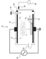
- FIG. 1 schematically shows a cross section of a metal oxide surface treatment apparatus 10 (hereinafter sometimes simply referred to as "surface treatment apparatus 10") according to an embodiment of the present application.
- the surface treatment apparatus 10 includes a processing vessel 12, an upper electrode 14, a lower electrode 16, a gas supply section 18, a high frequency power source 20, an exhaust port 22, an observation window 24, an emission detection section 26, and a recording section. 28.
- the surface treatment apparatus 10 treats the surface of the metal oxide 30 forming the electron transport layer of the object S to be treated with oxygen ions in oxygen plasma, which will be described later.
- the metals of the metal oxides are Al, Si, Sc with atomic number 21 to As with atomic number 33, Y with atomic number 38 to Sb with atomic number 51, and La with atomic number 57 to atomic number Up to Po of 84.
- the processing container 12 is made of a conductor material, such as an aluminum alloy, and is grounded.
- the upper electrode 14 is provided inside the processing container 12 and is made of a conductive material such as carbon.
- the lower electrode 16 is provided inside the processing container 12 so as to face the upper electrode 14 .
- the bottom electrode 16 is made of a conductive material such as carbon and is grounded.
- An object S to be processed is placed on the lower electrode 16 .
- the object S to be processed includes a transparent electrode layer 32 which is a constituent member of the perovskite solar cell C, and a layer of metal oxide 30 which is an electron transport layer formed on the transparent electrode layer 32 .
- a transparent electrode layer 32 and a layer of metal oxide 30 are laminated on a substrate 34 made of glass. Then, the object S to be processed is placed on the lower electrode 16 so that the layer of the metal oxide 30 is exposed.
- the gas supply unit 18 is connected to the processing container 12 and introduces oxygen gas G into the processing container 12 .
- a high frequency power supply 20 is electrically connected to the upper electrode 14 and the lower electrode 16 .
- the high-frequency power supply 20 applies a voltage having a frequency of 1 kHz or more and 40 kHz or less between the upper electrode 14 and the lower electrode 16, that is, supplies electric power.
- the oxygen gas G introduced between the upper electrode 14 and the lower electrode 16 from the gas supply section 18 is plasmatized to generate oxygen.
- Plasma PO is generated.
- oxygen plasma P 0 that is, oxygen radicals R 2 O and oxygen ions I 2 O can be efficiently generated. Further, by setting the frequency of the high-frequency power to 1 kHz or higher, the oxygen gas G can be turned into plasma.
- oxygen plasma is plasma generated from a gas containing 90 vol % or more of oxygen gas.
- the oxygen plasma is preferably a plasma generated from a gas containing 95 vol% or more of oxygen gas, more preferably a plasma generated from a gas containing 99 vol% or more of oxygen gas, and substantially composed of only oxygen gas. More preferably, the plasma is generated from a gas that
- Oxygen gas composed substantially only of oxygen is oxygen gas that does not contain impurities other than unavoidable impurities.
- oxygen gas supplied from a commercially available oxygen gas cylinder is oxygen gas substantially composed only of oxygen. Since the lower electrode 16 is grounded in the surface treatment apparatus 10, the oxygen ions I.sub.2O in the oxygen plasma P.sub.2O reach the surface of the metal oxide 30 considerably faster than the oxygen radicals R.sub.2O . The surface of the metal oxide 30 is modified by the oxygen ions I 2 O that have reached the surface of the metal oxide 30 .
- the exhaust port 22 discharges substances and oxygen radicals generated when the surface of the metal oxide 30 is treated with oxygen ions to the outside of the processing container 12 by an exhaust pump (not shown).
- Exhaust pumps include, for example, dry pumps, rotary pumps, or turbomolecular pumps that produce a high vacuum. In general, high vacuum increases the mean free path of plasma and improves plasma generation efficiency, so use of a turbo-molecular pump is preferred.
- the observation window 24 is a window for observing the inside of the processing container 12 from the outside, and is made of quartz, for example.
- the luminescence detector 26 detects luminescence within the processing container 12 .
- the light emission detector 26 is an optical fiber.
- the recording unit 28 is connected to the luminescence detection unit 26 to analyze and record luminescence within the processing container 12 .
- the recording unit 28 is a computer equipped with software for analyzing the type and intensity of light.
- the metal oxide surface treatment apparatus is a capacitively coupled plasma type metal oxide surface treatment apparatus, but instead of this, an inductively coupled plasma type metal oxide surface treatment apparatus is used. good too.
- An inductively coupled plasma type metal oxide surface treatment apparatus comprises: a dielectric processing container; an induction coil provided around the dielectric processing container; An electrode on which the object to be processed is installed so that the metal oxide layer of the object to be processed on which layers are laminated is exposed, a gas supply unit for introducing oxygen gas into the dielectric processing container, and a dielectric from the gas supply unit a high-frequency power supply having a frequency of 1 kHz or more and 40 kHz or less for supplying power to the induction coil so as to generate oxygen plasma from the oxygen gas introduced into the body treatment container.
- FIG. 2 schematically shows a cross section of the perovskite solar cell C.
- the perovskite solar cell C comprises a substrate 34, a transparent electrode layer 32, a layer of metal oxide 30 as an electron transport layer, a perovskite crystal layer 36 as a power generation layer, a hole transport layer 38, and an upper electrode layer 40. and , in that order.
- a perovskite crystal layer 36 is formed on the surface of the layer of metal oxide 30 .
- the perovskite solar cell C in addition to these constituent members, a diffusion prevention film provided on the light incident side of the substrate 34 and an interface between the metal oxide 30 layer as the electron transport layer and the perovskite crystal layer 36 are provided.
- An interface modification film or auxiliary layer, an interface modification film or auxiliary layer provided at the interface between the perovskite crystal layer 36 and the hole transport layer 38, or a sealing material and moisture for protecting the perovskite solar cell C from atmospheric moisture A getter material may be provided.
- the perovskite solar cell may be an inverted structure solar cell in which the electron transport layer and the hole transport layer in the perovskite solar cell C are exchanged. In this inverted structure solar cell, a structure in which the hole transport layer is a layer of metal oxide 30 and a perovskite crystal layer 36 is formed on the layer of metal oxide 30 can be adopted.
- the substrate 34 is a glass substrate
- the transparent electrode layer 32 is an FTO (fluorine-doped tin oxide) layer
- the metal oxide 30 layer is a tin oxide (SnO 2 ) layer composed of nanoparticles.
- the perovskite crystal layer 36 is Cs 0.05 (FA 0.89 MA 0.11 ) 0.95 Pb(I 0.89 Br 0.11 ) three layers (FA is formidinium, MA is methylamine (hereinafter the same) ),
- the hole-transporting layer 38 is a Spiro-OMeTAD (2,2′,7,7′-Tetrakis[N,N-di(4-methoxyphenyl)amino]-9,9′-spirobifluorene) layer
- the upper electrode layer 40 is a gold layer.
- a method for manufacturing a perovskite solar cell C according to an embodiment of the present application includes a transparent electrode layer, a metal oxide layer as an electron transport layer, a perovskite crystal layer as a power generation layer, a hole transport layer, and an upper electrode layer. , in this order, and the perovskite crystal layer is formed on the surface of the metal oxide layer.
- a method for manufacturing a perovskite solar cell according to another embodiment of the present application includes a transparent electrode layer, a metal oxide layer that is a hole transport layer, a perovskite crystal layer that is a power generation layer, an electron transport layer, and an upper electrode layer. are provided in this order, and the perovskite crystal layer is formed on the surface of the metal oxide layer.
- a method for manufacturing a perovskite solar cell according to each embodiment includes an oxygen plasma generation step, a metal oxide layer surface modification step, and a perovskite crystal layer formation step.
- the metal oxide 30 include titanium oxide and nickel oxide, in addition to tin oxide.
- perovskite crystals forming the perovskite crystal layer 36 in addition to Cs0.05 ( FA0.89MA0.11 ) 0.95Pb ( I0.89Br0.11 ) 3 , CH3NH3PbI3 and CH(NH 2 ) 2 PbI 3 and the like.
- the surface treatment apparatus 10 may be used, or another plasma treatment apparatus may be used.
- high-frequency power with a frequency of 1 kHz or more and 40 kHz or less is applied to generate oxygen plasma. More specifically, after cleaning the inside of the processing chamber 12 in advance with oxygen plasma, the object S to be processed is placed on the lower electrode 16, and the upper electrode 14 and the lower electrode are supplied from an oxygen tank connected to the gas supply unit 18. 16, the pressure in the processing container 12 is set to 50 Pa or more and 1200 Pa or less, and the power of 10 W is applied from the high frequency power supply 20 between the upper electrode 14 and the lower electrode 16 at a frequency of 1 kHz or more and 40 kHz or less. A high frequency power of 1000 W or more is supplied. Oxygen ions are efficiently generated by setting the power to 100 W or more and 1000 W or less.
- the supply of this high-frequency power converts the oxygen gas G into plasma, generating oxygen plasma PO .
- the pressure in the processing container 12 where the oxygen plasma P 2 O is generated is maintained at 1 Pa or more and 200 Pa or less, and the metal oxide layer surface modification step is performed. Oxygen ions are efficiently generated by setting the pressure to 1 Pa or more and 200 Pa or less.
- oxygen plasma P 2 O containing oxygen ions I 2 O was generated when the pressure in the processing container 12 was 500 Pa or less.
- this upper limit pressure varies depending on the surface treatment apparatus, the object to be treated, the concentration of the oxygen gas supplied into the treatment container, and the like. Therefore, as long as oxygen plasma P 2 O containing oxygen ions I 2 O can be generated, the pressure inside the processing container 12 is not particularly limited.
- the surface of the metal oxide 30 layer of the object S to be processed is irradiated with oxygen ions I 2 O in the oxygen plasma P 2 O to modify the surface of the metal oxide 30 layer.
- oxygen radicals R 2 O are not charged, they float between the upper electrode 14 and the lower electrode 16, and the surface of the metal oxide 30 is hardly irradiated.
- the surface of the metal oxide 30 after modification has substantially the same shape and a larger work function than the surface of the metal oxide 30 before modification.
- the surface of the metal oxide 30 is modified by the oxygen ions I 2 O , the surface of the metal oxide 30 is generated by plasma generated from a mixed gas of oxygen gas containing less than 90 vol % of oxygen gas and other gases. Processing time can be shortened compared to reforming.
- the surface modification can be performed in less than 40 seconds, whereas the treatment time is It takes 2 minutes or more for metal oxide surface modification using plasma of a mixed gas containing equal amounts of oxygen gas and argon gas, and 20 minutes or more for metal oxide surface modification by UV irradiation of ozone.
- the metal oxide surface treatment method of the embodiment of the present application includes the above oxygen plasma generation step and the above metal oxide surface modification step.
- the surface of the metal oxide is irradiated with oxygen ions in oxygen plasma to modify the surface of the metal oxide.
- This method for surface treatment of metal oxides is also a method for producing metal oxides whose surfaces have been modified.
- a perovskite crystal layer forming step a perovskite crystal layer is formed on the surface of the metal oxide layer modified in the metal oxide layer surface modification step.
- a perovskite crystal layer can be formed on the surface of the modified metal oxide layer by applying a perovskite crystal precursor to the surface of the modified metal oxide layer and drying it.
- a transparent electrode layer 32 is formed on a glass substrate 34 using a spin coating method, a sputtering method, a vacuum deposition method, a spray film forming method, a die coating method, a gravure printing method, a screen printing method, or the like.
- a metal oxide 30 is formed on the substrate, a hole transport layer 38 is formed on the perovskite crystal layer 36, and an upper electrode layer 40 is formed on the hole transport layer 38, respectively. These methods can also be employed when forming the perovskite crystal layer 36 on the layer of metal oxide 30 . The same is true for the reverse structure solar cell.
- a transparent electrode layer 32 is formed on a substrate 34 made of glass, and a metal oxide layer 30, which is a hole transport layer, is formed on the transparent electrode layer 32. , the perovskite crystal layer 36 on the metal oxide 30 layer, the electron transport layer on the perovskite crystal layer 36, and the upper electrode layer 40 on the electron transport layer.
- a plasma treatment apparatus (FEMTO (high-frequency power source frequency: 40 kHz, maximum power: 100 W), manufactured by Diener) having a structure as shown in FIG. 1 was used.
- a dry pump (ISP-50, manufactured by Anest Iwata Co., Ltd.) was connected to the exhaust port 22, and an oxygen cylinder (oxygen gas concentration: 99.5 vol%) was connected to the gas supply unit 18, respectively.
- Oxygen gas G was introduced into the processing container 12, and oxygen plasma P 2 O was generated so that the pressure in the processing container 12 was 10 different values ranging from 100 Pa to 1000 Pa.
- FIG. 3 shows an emission spectroscopic analysis chart at this time.
- Example 1 Surface Treatment of Tin Oxide with Oxygen Ions Surface treatment of tin oxide was performed using the plasma treatment apparatus of Reference Example. First, the FTO surface of glass with FTO (Nippon Sheet Glass Co., Ltd., NSG TEC 10) was dripped and spin-coated with a 15% by mass aqueous dispersion of tin (IV) oxide (Alfa Aesar) and dried at 150° C. for 1 hour. Thus, an object to be processed was obtained in which a glass substrate, an FTO layer as a transparent electrode layer, and a tin oxide layer as an electron transport layer were laminated in this order.
- this object to be processed was placed on the lower electrode so that the tin oxide faced the upper electrode.
- the pressure inside the processing container was reduced to 20 Pa or less by evacuation.
- oxygen gas was introduced into the processing chamber, the pressure in the processing chamber was maintained at 100 Pa, and high frequency power of 100 W was supplied between the upper electrode and the lower electrode to perform plasma cleaning for 30 seconds. rice field.
- the object to be processed was heated at 150°C for 1 hour.
- oxygen gas is introduced into the processing chamber, the pressure in the processing chamber is maintained at 100 Pa, high-frequency power of 100 W is supplied between the upper electrode and the lower electrode, and the oxygen gas is turned into plasma to generate oxygen plasma. let me This oxygen plasma contains oxygen radicals and oxygen ions as compared with the reference example. Then, the tin oxide was surface-treated for 30 seconds using oxygen ions in the oxygen plasma.
- Comparative Example 1 Surface Treatment of Tin Oxide with Ozone
- the surface treatment of tin oxide on the same object to be treated as in Example 1 was performed using a tabletop surface treatment apparatus (SSP16-110, Sen Special Light Source Co., Ltd.). First, this object to be processed was heated at 150° C. for 1 hour. Next, this object to be treated was placed in a desktop surface treatment apparatus. Then, the power of the UV light source was turned on, and the surface treatment of the tin oxide was performed for 20 minutes with ozone generated by the UV irradiation.
- SSP16-110 Sen Special Light Source Co., Ltd.
- Comparative Example 2 Surface Treatment of Tin Oxide with Oxygen Radicals Oxidation was carried out in the same manner as in Example 1, except that the pressure during oxygen plasma generation in Example 1 was changed to 1000 Pa and the surface treatment time was changed to 50 seconds. Tin surface treatment was performed. Oxygen plasma at a pressure of 1000 Pa contains only oxygen radicals compared to the reference example. Since the pressure inside the processing vessel is higher than in Example 1, the oxygen radicals descend quickly due to gravity, irradiate the object to be processed, and modify the surface of the tin oxide.
- Example 2 Evaluation of surface treatment of tin oxide (1) Work function of tin oxide By UPS (ultraviolet photoelectron spectroscopy), before surface treatment (untreated), Example 1, Comparative Example 1, and Comparative Example 2 The work function of the tin oxide surface after the surface treatment was calculated. The work functions of the tin oxide surfaces before the surface treatment and after the surface treatments of Example 1, Comparative Example 1, and Comparative Example 2 were 3.79 eV, 4.12 eV, 4.06 eV, and 4.04 eV, respectively. rice field. The surface treatment increased the work function of the tin oxide surface. Moreover, in Example 1, the work function of the tin oxide surface after the surface treatment was larger than in Comparative Examples 1 and 2. This is the effect of efficiently repairing oxygen defects in tin oxide with oxygen ions.
- UPS ultraviolet photoelectron spectroscopy
- the level of the conduction band of the perovskite crystal layer used in perovskite solar cells is generally between 3.5 eV and 4.5 eV, although it depends on the perovskite material.
- the work function of the metal oxide should be brought close to the level of the conduction band of the perovskite crystal layer, or the work function of the metal oxide is higher than the conduction band level of the perovskite crystal layer by about 0.2 eV. Since the work function of the tin oxide after the surface treatment of Example 1 was 4.12 eV, the electron extraction efficiency from this tin oxide to the perovskite crystal is high.
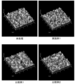
- the RMS of the tin oxide surface before the surface treatment and after the surface treatments of Example 1, Comparative Example 1, and Comparative Example 2 were 13.71 nm, 13.63 nm, 14.32 nm, and 12.72 nm, respectively. there were. From these similar RMS, it was found that the surface treatment did not cause damage that would change the surface shape of the tin oxide.
- Spiro-OMeTAD 61 mg of Spiro-OMeTAD and 10 mg of LiTFSI were dissolved in 0.7 mL of chlorobenzene, and 22 ⁇ L of 4-tert-butylpyridine was added to obtain a Spiro-OMeTAD precursor solution.
- This Spiro-OMeTAD precursor solution was applied to the surface of each of the Cs 0.05 (FA 0.89 MA 0.11 ) 0.95 Pb(I 0.89 Br 0.11 ) three layers obtained above at 3000 rpm. Spin coated for 30 seconds. Then, it was dried at 65° C. for 10 minutes to form a Spiro-OMeTAD layer.
- a gold layer having a thickness of 50 nm was deposited on the surface of these Spiro-OMeTAD layers using a vacuum deposition machine to obtain a solar cell member.
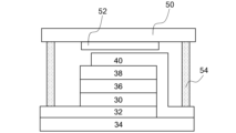
- FIG. 6 schematically shows a cross section of these perovskite solar cells.
- These perovskite solar cells were irradiated with simulated AM 1.5 sunlight (intensity 1000 W/m 2 ) using a solar simulator (OTENTO-SUN, manufactured by Spectroscopic Instruments Co., Ltd.).
- a short-circuit current density, an open-circuit voltage, a fill factor, and a photoelectric conversion efficiency were obtained from a curve plotting a current-voltage relationship using a source meter (Keithley 2400, manufactured by Keithley Instruments (hereinafter the same)). Table 1 shows the results.
- the perovskite solar cell manufactured from the processed material obtained in Example 1 had a higher open-circuit voltage than the perovskite solar cell manufactured from the processed material obtained in Comparative Example 1. .
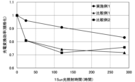
- the light durability of the perovskite solar cells produced from the objects to be treated obtained in Example 1, Comparative Example 1, and Comparative Example 2 was evaluated.
- these perovskite solar cells were continuously irradiated with AM1.5 simulated sunlight (intensity 1000 W/m 2 ) at 25° C. and 30% humidity.
- the photoelectric conversion efficiency was obtained from a curve obtained by plotting the current-voltage relationship with a source meter at predetermined time intervals, and the ratio between the obtained photoelectric conversion efficiency and the initial photoelectric conversion efficiency was calculated. The results are shown in FIG. As shown in FIG.
- the perovskite solar cell manufactured from the object to be processed obtained in Example 1 had higher light durability than other perovskite solar cells. This is because the oxygen deficiency on the surface of the tin oxide was repaired by the surface treatment of the tin oxide in Example 1, and the light durability centering on the visible light region was improved.
- Example 3 Surface Treatment of Titanium Oxide with Oxygen Ions
- a titanium diisopropoxide acetylacetonate solution (Aldrich Co.) was diluted with ethanol so that the concentration of this titanium compound was 6% by mass to prepare a titanium oxide precursor solution. got In an environment of 400° C., this titanium oxide precursor liquid was sprayed onto the FTO surface of a glass with FTO (NSG TEC 10, Nippon Sheet Glass Co., Ltd.) using an air brush, and dried at 500° C. for 10 minutes to form a glass substrate, An object to be treated was obtained in which an FTO layer and a titanium oxide layer used as an electron transport layer of a regular structure perovskite solar cell were laminated in this order. In the same manner as in Example 1, the titanium oxide surface of this object to be treated was treated with oxygen ions.
- Comparative Example 3 Surface Treatment of Titanium Oxide with Ozone An object to be treated having a layer of titanium oxide was obtained in the same manner as in Example 3, and the surface of the titanium oxide of the object to be treated was treated with ozone in the same manner as in Comparative Example 1. processed.
- Comparative Example 4 Surface Treatment of Titanium Oxide with Oxygen Radicals An object to be treated having a layer of titanium oxide was obtained in the same manner as in Example 3, and the titanium oxide surface of the object to be treated was treated in the same manner as in Comparative Example 2. Oxygen radical treatment.
- Example 4 Evaluation of surface treatment of titanium oxide
- titanium oxide before surface treatment (untreated) and after surface treatment of Example 3, Comparative Example 3, and Comparative Example 4 We calculated the work function of the surface of The work functions of the titanium oxide surfaces before the surface treatment and after the surface treatments of Example 2, Comparative Example 3, and Comparative Example 4 were 3.87 eV, 4.12 eV, 4.27 eV, and 4.34 eV, respectively. rice field.
- the surface treatment increased the work function of the titanium oxide surface.
- the work function of the titanium oxide surface after the surface treatment was larger than in Comparative Examples 3 and 4. This is the effect of efficiently repairing oxygen defects in titanium oxide with oxygen ions.
- the work function of the titanium oxide after the surface treatment in Example 3 was 4.12 eV, so the electron extraction efficiency from this titanium oxide to the perovskite crystal is high.
- Example 5 Surface Treatment of Nickel Oxide with Oxygen Ions
- Nickel oxide used as a hole-transporting layer for an inverse structure perovskite solar cell was performed.
- FTO surface of glass with FTO Nippon Sheet Glass Co., Ltd., NSG TEC 10
- AVANTAMA 2.5 mass% ethanol dispersion of nickel oxide
- an object to be processed in which the glass substrate, the FTO layer, and the nickel oxide layer were laminated in this order was obtained.
- Comparative Example 5 Surface Treatment of Nickel Oxide with Ozone An object to be treated having a nickel oxide layer was obtained in the same manner as in Example 5, and the nickel oxide surface of the object to be treated was treated with ozone in the same manner as in Comparative Example 1. processed.
- Comparative Example 6 Surface Treatment of Nickel Oxide with Oxygen Radicals An object to be treated having a layer of nickel oxide was obtained in the same manner as in Example 5, and the nickel oxide surface of the object to be treated was treated in the same manner as in Comparative Example 2. Oxygen radical treatment.
- Example 6 Evaluation of surface treatment of nickel oxide
- nickel oxide before surface treatment (untreated) and after surface treatment of Example 5, Comparative Example 5, and Comparative Example 6 We calculated the work function of the surface of The work functions of the nickel oxide surfaces before the surface treatment and after the surface treatments of Example 5, Comparative Example 5, and Comparative Example 6 were 5.16 eV, 5.43 eV, 5.59 eV, and 5.52 eV, respectively. rice field.
- the surface treatment increased the work function of the nickel oxide surface.
- the valence band level of the perovskite crystal layer used in perovskite solar cells depends on the perovskite material, but is generally between 4.5 eV and 6.0 eV. be. In order to reduce the interfacial resistance between the perovskite crystal and the metal oxide and improve the hole extraction efficiency, it is preferable to bring the work function of the metal oxide closer to the level of the valence band of the perovskite crystal layer. Since the work function of the nickel oxide after the surface treatment of Example 5 was 5.43 eV, the hole extraction efficiency from this nickel oxide to the perovskite crystal is high.
Landscapes
- Physics & Mathematics (AREA)
- Electromagnetism (AREA)
- Engineering & Computer Science (AREA)
- Chemical & Material Sciences (AREA)
- Materials Engineering (AREA)
- Plasma & Fusion (AREA)
- Spectroscopy & Molecular Physics (AREA)
- Inorganic Chemistry (AREA)
- Manufacturing & Machinery (AREA)
- Photovoltaic Devices (AREA)
Priority Applications (2)
| Application Number | Priority Date | Filing Date | Title |
|---|---|---|---|
| JP2023572427A JP7740739B2 (ja) | 2022-01-06 | 2022-12-22 | 金属酸化物の表面処理方法、ペロブスカイト太陽電池の製造方法、および金属酸化物表面処理装置 |
| KR1020247021434A KR102923263B1 (ko) | 2022-01-06 | 2022-12-22 | 페로브스카이트 태양 전지의 제조 방법, 및 금속 산화물 표면 처리 장치 |
Applications Claiming Priority (2)
| Application Number | Priority Date | Filing Date | Title |
|---|---|---|---|
| JP2022-000890 | 2022-01-06 | ||
| JP2022000890 | 2022-01-06 |
Publications (1)
| Publication Number | Publication Date |
|---|---|
| WO2023132259A1 true WO2023132259A1 (ja) | 2023-07-13 |
Family
ID=87073568
Family Applications (1)
| Application Number | Title | Priority Date | Filing Date |
|---|---|---|---|
| PCT/JP2022/047340 Ceased WO2023132259A1 (ja) | 2022-01-06 | 2022-12-22 | 金属酸化物の表面処理方法、ペロブスカイト太陽電池の製造方法、および金属酸化物表面処理装置 |
Country Status (3)
| Country | Link |
|---|---|
| JP (1) | JP7740739B2 (https=) |
| KR (1) | KR102923263B1 (https=) |
| WO (1) | WO2023132259A1 (https=) |
Cited By (2)
| Publication number | Priority date | Publication date | Assignee | Title |
|---|---|---|---|---|
| CN118932314A (zh) * | 2024-07-23 | 2024-11-12 | 中山大学 | 一种晶体硅-宽带隙化合物异质结太阳电池制备方法 |
| WO2025127101A1 (ja) * | 2023-12-15 | 2025-06-19 | Toppanホールディングス株式会社 | 太陽電池、ナノ材料、及び分散液、並びに太陽電池の製造方法 |
Citations (12)
| Publication number | Priority date | Publication date | Assignee | Title |
|---|---|---|---|---|
| JP2001284060A (ja) * | 2000-03-29 | 2001-10-12 | Honda Motor Co Ltd | 透明電極および有機エレクトロルミネッセンス素子 |
| JP2008159347A (ja) * | 2006-12-22 | 2008-07-10 | Seiko Epson Corp | 透明導電膜の製造方法、有機エレクトロルミネッセンス装置の製造方法、およびプラズマ処理装置 |
| JP2008205254A (ja) * | 2007-02-21 | 2008-09-04 | Toyota Central R&D Labs Inc | 有機電界発光素子 |
| JP2009224596A (ja) * | 2008-03-17 | 2009-10-01 | Tokyo Electron Ltd | プラズマ処理装置 |
| JP2010037648A (ja) * | 2008-07-09 | 2010-02-18 | Univ Of Tokyo | 無機薄膜及びその製造方法、並びにガラス |
| US20120132272A1 (en) * | 2010-11-19 | 2012-05-31 | Alliance For Sustainable Energy, Llc. | Solution processed metal oxide thin film hole transport layers for high performance organic solar cells |
| JP2013534057A (ja) * | 2010-06-30 | 2013-08-29 | コーニング インコーポレイテッド | Soi基板に仕上げを施す方法 |
| JP2013191423A (ja) * | 2012-03-14 | 2013-09-26 | Toshiba Corp | プラズマ処理装置 |
| CN108054282A (zh) * | 2017-11-27 | 2018-05-18 | 济南大学 | 锌掺杂氧化镍纳米颗粒空穴传输层反置钙钛矿太阳能电池及制备方法 |
| CN109841740A (zh) * | 2019-03-22 | 2019-06-04 | 上海交通大学 | 一种基于氧化镍空穴传输层的钙钛矿太阳电池的制备方法 |
| CN111540835A (zh) * | 2020-05-11 | 2020-08-14 | 北京工业大学 | 一种提高钙钛矿太阳能电池热稳定性的方法 |
| CN112397654A (zh) * | 2020-11-16 | 2021-02-23 | 西交利物浦大学 | 钙钛矿太阳能电池及其制备方法 |
Family Cites Families (7)
| Publication number | Priority date | Publication date | Assignee | Title |
|---|---|---|---|---|
| JP2000133466A (ja) * | 1998-10-23 | 2000-05-12 | Canon Inc | 表面改質ito膜、その表面処理方法およびそれを用いた電荷注入型発光素子 |
| JP2001284059A (ja) | 2000-03-29 | 2001-10-12 | Honda Motor Co Ltd | 透明電極、有機エレクトロルミネッセンス素子、透明電極処理装置および透明電極の処理方法 |
| FR2913146B1 (fr) * | 2007-02-23 | 2009-05-01 | Saint Gobain | Electrode discontinue, dispositif electroluminescent organique l'incorporant, et leurs fabrications |
| JP2008234896A (ja) * | 2007-03-19 | 2008-10-02 | Seiko Epson Corp | 有機エレクトロルミネッセンス装置の製造方法 |
| CN102610765A (zh) * | 2012-04-06 | 2012-07-25 | 复旦大学 | 一种提高氧化铟锡透明导电膜表面功函数的表面修饰方法 |
| JP6685142B2 (ja) * | 2016-02-02 | 2020-04-22 | 株式会社ジャパンディスプレイ | 表示装置及びその製造方法 |
| CN111081812A (zh) * | 2019-11-18 | 2020-04-28 | 深圳第三代半导体研究院 | 一种透明导电氧化物薄膜的制备方法及应用 |
-
2022
- 2022-12-22 WO PCT/JP2022/047340 patent/WO2023132259A1/ja not_active Ceased
- 2022-12-22 JP JP2023572427A patent/JP7740739B2/ja active Active
- 2022-12-22 KR KR1020247021434A patent/KR102923263B1/ko active Active
Patent Citations (12)
| Publication number | Priority date | Publication date | Assignee | Title |
|---|---|---|---|---|
| JP2001284060A (ja) * | 2000-03-29 | 2001-10-12 | Honda Motor Co Ltd | 透明電極および有機エレクトロルミネッセンス素子 |
| JP2008159347A (ja) * | 2006-12-22 | 2008-07-10 | Seiko Epson Corp | 透明導電膜の製造方法、有機エレクトロルミネッセンス装置の製造方法、およびプラズマ処理装置 |
| JP2008205254A (ja) * | 2007-02-21 | 2008-09-04 | Toyota Central R&D Labs Inc | 有機電界発光素子 |
| JP2009224596A (ja) * | 2008-03-17 | 2009-10-01 | Tokyo Electron Ltd | プラズマ処理装置 |
| JP2010037648A (ja) * | 2008-07-09 | 2010-02-18 | Univ Of Tokyo | 無機薄膜及びその製造方法、並びにガラス |
| JP2013534057A (ja) * | 2010-06-30 | 2013-08-29 | コーニング インコーポレイテッド | Soi基板に仕上げを施す方法 |
| US20120132272A1 (en) * | 2010-11-19 | 2012-05-31 | Alliance For Sustainable Energy, Llc. | Solution processed metal oxide thin film hole transport layers for high performance organic solar cells |
| JP2013191423A (ja) * | 2012-03-14 | 2013-09-26 | Toshiba Corp | プラズマ処理装置 |
| CN108054282A (zh) * | 2017-11-27 | 2018-05-18 | 济南大学 | 锌掺杂氧化镍纳米颗粒空穴传输层反置钙钛矿太阳能电池及制备方法 |
| CN109841740A (zh) * | 2019-03-22 | 2019-06-04 | 上海交通大学 | 一种基于氧化镍空穴传输层的钙钛矿太阳电池的制备方法 |
| CN111540835A (zh) * | 2020-05-11 | 2020-08-14 | 北京工业大学 | 一种提高钙钛矿太阳能电池热稳定性的方法 |
| CN112397654A (zh) * | 2020-11-16 | 2021-02-23 | 西交利物浦大学 | 钙钛矿太阳能电池及其制备方法 |
Cited By (2)
| Publication number | Priority date | Publication date | Assignee | Title |
|---|---|---|---|---|
| WO2025127101A1 (ja) * | 2023-12-15 | 2025-06-19 | Toppanホールディングス株式会社 | 太陽電池、ナノ材料、及び分散液、並びに太陽電池の製造方法 |
| CN118932314A (zh) * | 2024-07-23 | 2024-11-12 | 中山大学 | 一种晶体硅-宽带隙化合物异质结太阳电池制备方法 |
Also Published As
| Publication number | Publication date |
|---|---|
| JPWO2023132259A1 (https=) | 2023-07-13 |
| KR20240112915A (ko) | 2024-07-19 |
| JP7740739B2 (ja) | 2025-09-17 |
| KR102923263B1 (ko) | 2026-02-04 |
Similar Documents
| Publication | Publication Date | Title |
|---|---|---|
| JP6624257B2 (ja) | 電子デバイスおよびその製造方法 | |
| JP3671183B2 (ja) | 色素増感型太陽電池の製造方法 | |
| WO2023132259A1 (ja) | 金属酸化物の表面処理方法、ペロブスカイト太陽電池の製造方法、および金属酸化物表面処理装置 | |
| Mozaffari et al. | An investigation on the effect of electrodeposited nanostructured ZnO on the electron transfer process efficiency of TiO2 based DSSC | |
| Peiris et al. | Stacked rGO–TiO2 photoanode via electrophoretic deposition for highly efficient dye-sensitized solar cells | |
| CN104404512A (zh) | 一种高稳定性可循环使用表面增强拉曼基底及制备方法 | |
| CN106732807A (zh) | 一种二氧化钛‑有机钙钛矿复合光催化薄膜及制备和应用 | |
| Huang et al. | Performance improvement of dye-sensitized solar cells by using TiO2 compact layer and silver nanowire scattering layer | |
| CN119677305A (zh) | 一种可扩展复合空穴传输层及基于其的钙钛矿太阳能电池 | |
| Sudhagar et al. | Interfacial engineering of quantum dot-sensitized TiO 2 fibrous electrodes for futuristic photoanodes in photovoltaic applications | |
| Hvojnik et al. | The effect of rapid atmospheric plasma treatment of FTO substrates on the quality of TiO2 blocking layers for printed perovskite solar cells | |
| US8765520B2 (en) | Methods of manufacturing photovoltaic electrodes | |
| Hashimoto et al. | Effect of oxygen plasma treatment of indium tin oxide for organic solar cell | |
| CN113668029B (zh) | 粗糙金纳米颗粒构成的薄膜及其制备方法和用途 | |
| CN116404049A (zh) | 石墨烯钝化的无机钙钛矿太阳能电池及其制备方法 | |
| CN103310992A (zh) | 一种染料敏化太阳能电池的光阳极及其制备方法 | |
| Shahzad et al. | In-situ spectroscopic analyses of the dye uptake on ZnO and TiO2 photoanodes for dye-sensitized solar cells | |
| CN115224199A (zh) | 钙钛矿太阳能电池及其制备方法 | |
| Jung et al. | Solar conversion efficiency improvement of dye-sensitized solar cells via plasma treatment of transparent conducting oxide substrate | |
| TWI820777B (zh) | 光電化學裝置 | |
| US20240372032A1 (en) | Method for preparing heterojunction cell, heterojunction cell and photovoltaic assembly | |
| Ramachandran et al. | Photovoltaic studies of dye sensitized solar cells fabricated from microwave exposed photo anodes | |
| CN120099606A (zh) | 一种紫外光刻设备透镜支架组件的表面处理方法 | |
| Ganchev et al. | Tin dioxide thin films deposited by sol–gel technique | |
| KR101026418B1 (ko) | 광전극 및 이의 형성 방법 |
Legal Events
| Date | Code | Title | Description |
|---|---|---|---|
| 121 | Ep: the epo has been informed by wipo that ep was designated in this application |
Ref document number: 22918843 Country of ref document: EP Kind code of ref document: A1 |
|
| ENP | Entry into the national phase |
Ref document number: 2023572427 Country of ref document: JP Kind code of ref document: A |
|
| ENP | Entry into the national phase |
Ref document number: 20247021434 Country of ref document: KR Kind code of ref document: A |
|
| WWE | Wipo information: entry into national phase |
Ref document number: 1020247021434 Country of ref document: KR |
|
| NENP | Non-entry into the national phase |
Ref country code: DE |
|
| 122 | Ep: pct application non-entry in european phase |
Ref document number: 22918843 Country of ref document: EP Kind code of ref document: A1 |