WO2023127110A1 - 光検出装置及び電子機器 - Google Patents
光検出装置及び電子機器 Download PDFInfo
- Publication number
- WO2023127110A1 WO2023127110A1 PCT/JP2021/048832 JP2021048832W WO2023127110A1 WO 2023127110 A1 WO2023127110 A1 WO 2023127110A1 JP 2021048832 W JP2021048832 W JP 2021048832W WO 2023127110 A1 WO2023127110 A1 WO 2023127110A1
- Authority
- WO
- WIPO (PCT)
- Prior art keywords
- light
- layer
- semiconductor layer
- photoelectric conversion
- photodetector
- Prior art date
- Legal status (The legal status is an assumption and is not a legal conclusion. Google has not performed a legal analysis and makes no representation as to the accuracy of the status listed.)
- Ceased
Links
Images






Classifications
-
- H—ELECTRICITY
- H10—SEMICONDUCTOR DEVICES; ELECTRIC SOLID-STATE DEVICES NOT OTHERWISE PROVIDED FOR
- H10F—INORGANIC SEMICONDUCTOR DEVICES SENSITIVE TO INFRARED RADIATION, LIGHT, ELECTROMAGNETIC RADIATION OF SHORTER WAVELENGTH OR CORPUSCULAR RADIATION
- H10F30/00—Individual radiation-sensitive semiconductor devices in which radiation controls the flow of current through the devices, e.g. photodetectors
- H10F30/20—Individual radiation-sensitive semiconductor devices in which radiation controls the flow of current through the devices, e.g. photodetectors the devices having potential barriers, e.g. phototransistors
-
- H—ELECTRICITY
- H10—SEMICONDUCTOR DEVICES; ELECTRIC SOLID-STATE DEVICES NOT OTHERWISE PROVIDED FOR
- H10F—INORGANIC SEMICONDUCTOR DEVICES SENSITIVE TO INFRARED RADIATION, LIGHT, ELECTROMAGNETIC RADIATION OF SHORTER WAVELENGTH OR CORPUSCULAR RADIATION
- H10F39/00—Integrated devices, or assemblies of multiple devices, comprising at least one element covered by group H10F30/00, e.g. radiation detectors comprising photodiode arrays
- H10F39/10—Integrated devices
- H10F39/12—Image sensors
Definitions
- the present disclosure relates to a photodetector and an electronic device equipped with this photodetector.
- an imaging element provided in an image sensor for detecting visible light such as red light (R), green light (G), and blue light (B) is usually a light receiving element formed on a silicon semiconductor substrate. It has an element (photodiode).
- R red light
- G green light
- B blue light
- IR infrared light
- InGaAs image sensors that can detect infrared light by using InGaAs instead of silicon. It is known that this InGaAs image sensor is formed by forming an InGaAs film on an InP substrate, and light is incident from the InP substrate side. However, the InGaAs image sensor cannot detect visible light unless the InP substrate on the light incident side is removed.
- Patent Document 1 there is a known method of increasing the visible light sensitivity of an InGaAs image sensor by thinning the n+InP layer (recombination prevention layer that suppresses the generation of dark current) on the light incident side.
- the damage during the process reaches the narrow bandgap InGaAs layer, causing crystal defects and white spots.
- the impurity concentration of the InP layer on the light incident side photoelectric conversion is possible in the InP layer, and visible light sensitivity does not easily decrease even if the thickness of the InP layer is increased. become white scars.
- the present disclosure has been made in view of such circumstances, and an object thereof is to provide a photodetector and an electronic device capable of making it difficult for crystal defects to occur while maintaining visible light sensitivity.
- One aspect of the present disclosure includes a pixel region in which a plurality of pixels capable of generating an electric signal in response to externally incident infrared light and visible light are arranged in a matrix, and the pixel region contains a first compound A light transmission layer made of a semiconductor and transmitting incident infrared light; and a photoelectric conversion layer that photoelectrically converts infrared light transmitted through the light transmission layer, the light transmission layer being provided on the light incident surface side and having a thickness capable of transmitting the visible light.
- the semiconductor layer 2 has an impurity concentration lower than that of the first semiconductor layer and higher than that of the photoelectric conversion layer.
- Another aspect of the present disclosure includes a pixel region in which a plurality of pixels capable of generating an electric signal in response to externally incident infrared light and visible light are arranged in a matrix, and the pixel region includes a first A light-transmitting layer made of a compound semiconductor and transmitting incident infrared light; and a second compound semiconductor different from the first compound semiconductor, laminated on a surface of the light-transmitting layer opposite to the light incident surface. and a photoelectric conversion layer that photoelectrically converts infrared light transmitted through the light transmission layer, the light transmission layer being provided on the light incident surface side and having a thickness capable of transmitting the visible light.
- the second semiconductor layer has a lower impurity concentration than the first semiconductor layer and a higher impurity concentration than the photoelectric conversion layer.
- FIG. 1 is a schematic plan layout diagram showing a configuration example of a photodetector according to a first embodiment of the present disclosure
- FIG. 1 is a block diagram showing a configuration example of a photodetector according to a first embodiment of the present disclosure
- FIG. 2 is a circuit diagram showing a configuration example of a readout circuit of the photodetector according to the first embodiment of the present disclosure
- FIG. 1 is a schematic cross-sectional view of a principal part showing a configuration example of a photodetector according to a first embodiment of the present disclosure
- FIG. FIG. 4 is a characteristic diagram showing the dependence of InP film thickness and light transmittance;
- FIG. 1 is a schematic plan layout diagram showing a configuration example of a photodetector according to a first embodiment of the present disclosure
- FIG. 1 is a block diagram showing a configuration example of a photodetector according to a first embodiment of the present disclosure
- FIG. 2 is a circuit diagram showing a configuration example
- FIG. 10 is a cross-sectional view of a photodetector showing an example of the occurrence of process damage in a comparative example
- FIG. 10 is a cross-sectional view of a photodetector showing another example of occurrence of process damage in a comparative example
- FIG. 4 is a diagram for explaining how carriers photoelectrically converted with visible light are transferred to the photoelectric conversion layer in the first embodiment of the present disclosure
- FIG. 4 is a diagram shown for explaining how process damage becomes difficult to reach a photoelectric conversion layer in the first embodiment of the present disclosure
- FIG. 4 is a cross-sectional view of a photodetector according to a second embodiment of the present disclosure
- FIG. 5 is a cross-sectional view of a photodetector according to a third embodiment of the present disclosure
- FIG. 11 is a cross-sectional view of a photodetector according to a fourth embodiment of the present disclosure
- FIG. 11 is a cross-sectional view of a photodetector according to a fifth embodiment of the present disclosure
- FIG. 11 is a cross-sectional view of a photodetector according to a sixth embodiment of the present disclosure
- FIG. 3 is a schematic plan view showing an arrangement pattern of pixels for infrared light and pixels for infrared light and visible light. It is a block diagram showing a configuration example of an electronic device to which the present technology is applied.
- 1 is a block diagram showing an example of a schematic configuration of a vehicle control system
- FIG. FIG. 4 is an explanatory diagram showing an example of installation positions of an outside information detection unit and an imaging unit;
- first conductivity type is one of p-type or n-type
- second conductivity type means one of p-type or n-type, which is different from “first conductivity type”.
- first conductivity type is one of p-type or n-type
- second conductivity type means one of p-type or n-type, which is different from “first conductivity type”.
- “+” and “-” attached to "n” and “p” refer to semiconductor regions having relatively high or low impurity densities, respectively, compared to semiconductor regions not marked with “+” and “-”. It means that it is an area. However, even if the same "n” is attached to the semiconductor region, it does not mean that the impurity density of each semiconductor region is exactly the same.
- FIG. 1 is a schematic plan layout diagram showing one configuration example of a photodetector according to the first embodiment of the present disclosure.
- a photodetector 1A according to the first embodiment of the present disclosure mainly includes a semiconductor chip 2 having a square two-dimensional planar shape when viewed in plan. That is, the photodetector 1A is mounted on the semiconductor chip 2.
- FIG. This photodetector 1A takes in incident light from a subject through an optical lens (not shown), converts the light amount of the incident light formed into an image on an imaging surface into an electric signal for each pixel, and obtains a pixel signal. Output.
- the semiconductor chip 2 on which the photodetector 1A is mounted has, in a two-dimensional plane, a rectangular pixel region 2A provided in the center and a peripheral region arranged outside the pixel region 2A so as to surround the pixel region 2A. 2B.
- the pixel area 2A is, for example, a light receiving surface that receives light condensed by an optical lens.
- a plurality of pixels 3 are arranged in a matrix on a two-dimensional plane including the X direction and the Y direction.
- the pixels 3 are repeatedly arranged in the X direction and the Y direction that are orthogonal to each other within the two-dimensional plane.
- a plurality of bonding pads (input/output terminals) 14 are arranged in the peripheral region 2B. Each of the plurality of bonding pads 14 is arranged, for example, along four sides of the two-dimensional plane of the semiconductor chip 2 . Each of the plurality of bonding pads 14 is an input/output terminal used when electrically connecting the semiconductor chip 2 to an external device.
- FIG. 2 is a block diagram showing a configuration example of the photodetector 1A.
- the semiconductor chip 2 includes a logic circuit 13 including a vertical drive circuit 4, a column signal processing circuit 5, a horizontal drive circuit 6, an output circuit 7, a control circuit 8, and the like.
- the logic circuit 13 is composed of, for example, a CMOS (Complementary MOS) circuit having an n-channel conductivity type MOSFET (Metal Oxide Semiconductor Field Effect Transistor) and a p-channel conductivity type MOSFET.
- CMOS Complementary MOS
- MOSFET Metal Oxide Semiconductor Field Effect Transistor
- the vertical driving circuit 4 is composed of, for example, a shift register.
- the vertical drive circuit 4 sequentially selects desired pixel drive wirings 10, supplies pulses for driving the pixels 3 to the selected pixel drive wirings 10, and drives the pixels 3 row by row. That is, the vertical drive circuit 4 sequentially selectively scans the pixels 3 in the pixel region 2A in the vertical direction row by row, and outputs signals from the pixels 3 based on the signal charges generated by the photoelectric conversion elements of the pixels 3 according to the amount of received light.
- a pixel signal is supplied to the column signal processing circuit 5 through the vertical signal wiring 11 .
- the column signal processing circuit 5 is arranged, for example, for each column of the pixels 3, and performs signal processing such as noise removal on the signals output from the pixels 3 of one row for each pixel column.
- the column signal processing circuit 5 performs signal processing such as CDS (Correlated Double Sampling) and AD (Analog Digital) conversion for removing pixel-specific fixed pattern noise.
- the horizontal driving circuit 6 is composed of, for example, a shift register.
- the horizontal driving circuit 6 sequentially outputs a horizontal scanning pulse to the column signal processing circuit 5 to select each of the column signal processing circuits 5 in order, and the pixels subjected to the signal processing from each of the column signal processing circuits 5 are selected.
- a signal is output to the horizontal signal wiring 12 .
- the output circuit 7 performs signal processing on the pixel signals sequentially supplied from each of the column signal processing circuits 5 through the horizontal signal wiring 12 and outputs the processed signals.
- signal processing for example, buffering, black level adjustment, column variation correction, and various digital signal processing can be used.
- the control circuit 8 generates a clock signal and a control signal that serve as references for the operation of the vertical drive circuit 4, the column signal processing circuit 5, the horizontal drive circuit 6, etc. based on the vertical synchronization signal, the horizontal synchronization signal, and the master clock signal. Generate. The control circuit 8 then outputs the generated clock signal and control signal to the vertical drive circuit 4, the column signal processing circuit 5, the horizontal drive circuit 6, and the like.
- FIG. 3 is a circuit diagram showing a configuration example of the readout circuit 15 of the photodetector 1A.
- Each pixel 3 of the plurality of pixels has a photoelectric conversion element PD.
- a readout circuit 15 is connected to the photoelectric conversion element PD of each pixel 3 .
- the photoelectric conversion element PD generates charges (signal charges) corresponding to the amount of light received.
- a predetermined bias voltage Va is applied to the cathode side of the photoelectric conversion element PD.
- the readout circuit 15 is connected to the anode side of the photoelectric conversion element PD.
- the readout circuit 15 has a capacitive element Cp as a charge storage section (charge holding section), a reset transistor RST, an amplification transistor AMP, and a selection transistor SEL.
- These transistors (RST, AMP, SEL) are composed of MOSFETs having a silicon oxide film as a gate insulating film, for example.
- these transistors (RST, AMP, SEL) may be MISFETs (Metal Insulator Semiconductor FETs) whose gate insulating film is a silicon nitride (Si3N4) film or a laminated film of silicon nitride film and silicon oxide film.
- the capacitive element Cp accumulates signal charges generated by the photoelectric conversion element PD.
- the capacitive element Cp is composed of, for example, any one of pn junction capacitance, MOS capacitance, and wiring capacitance.
- the amplification transistor AMP outputs a pixel signal corresponding to the accumulated potential of the capacitive element Cp.
- the amplification transistor AMP constitutes a load MOS as a constant current source and a source follower circuit, which are connected via the vertical signal wiring 11 .
- the source follower circuit outputs a pixel signal indicating a level corresponding to the signal charge accumulated in the capacitive element Cp from the amplification transistor AMP to the column signal processing circuit 5 via the selection transistor SEL and the vertical signal line 11 .
- the selection transistor SEL outputs the pixel signal of the pixel 3 to the column signal processing circuit 5 through the vertical signal wiring 11 when the selection signal is applied to the gate electrode and the selection transistor SEL is turned on.
- a signal line to which the selection signal is transferred and a signal line to which the reset signal is transferred correspond to the pixel drive line 10 in FIG.
- FIG. 4 is a schematic cross-sectional view of a main part showing one configuration example of the photodetector 1A.
- the semiconductor chip 2 includes a photoelectric conversion board portion 20 and a circuit board portion 40 which are laminated facing each other.
- the photoelectric conversion substrate section 20 includes the above-described pixel region 2A and the like.
- the circuit board portion 40 includes the above-described logic circuit 13, bonding pads 14, readout circuit 15, and the like.
- the photoelectric conversion substrate portion 20 is arranged on a first compound semiconductor layer 25 having a first surface 25x and a second surface 25y opposite to each other, and on the second surface 25y side of the first compound semiconductor layer 25. and a second compound semiconductor layer 23. and a recombination prevention layer 22 as a second compound semiconductor layer arranged on the second surface 23y side of the second compound semiconductor layer 23 .
- Each of the first compound semiconductor layer 25 , the second compound semiconductor layer 23 and the recombination prevention layer 22 is commonly provided for each pixel 3 .
- the above-described photoelectric conversion element PD is provided for each pixel 3 in the first compound semiconductor layer 25 .
- the recombination prevention layer 22 suppresses dark current generation.
- the first surface 25x of the first compound semiconductor layer 25 is sometimes called an element forming surface or main surface
- the second surface 25y is sometimes called a light incident surface or a rear surface
- the first surface 23x and the second surface 23y located on opposite sides of the second compound semiconductor layer 23 the first surface 23x is the main surface and the second surface 23y is the light incident surface or the rear surface. sometimes called.
- the photoelectric conversion substrate section 20 further includes a protective film 29 on the first surface 25x side of the first compound semiconductor layer 25 to cover the first surface 25x.
- the protective film 29 is provided in common for each pixel 3 .
- the photoelectric conversion substrate section 20 includes a light shielding film (not shown), an antireflection film (not shown), a planarizing film (not shown), and a light-incident surface of the recombination prevention layer 22.
- a microlens (on-chip lens) 57 is further provided.
- the recombination prevention layer 22 and the second compound semiconductor layer 23 constitute a light transmission layer that transmits light with wavelengths in the infrared region (infrared light 61) and light with wavelengths in the visible region (visible light 62).
- the first compound semiconductor layer 25 includes, for example, a photoelectric conversion layer 26 and a cap layer 27 from the first surface 25x side.
- the recombination prevention layer 22, the second compound semiconductor layer 23, the photoelectric conversion layer 26 of the first compound semiconductor layer 25, and the cap layer 27 are epitaxially grown on a growth substrate (not shown) in this order. layer. That is, in the first compound semiconductor layer 25 , the photoelectric conversion layer 26 and the cap layer 27 are covalently bonded, and the photoelectric conversion layer 26 is covalently bonded to the second compound semiconductor layer 23 .
- the cap layer 27 is, for example, commonly provided for all the pixels 3 and arranged between the protective film 29 and the photoelectric conversion layer 26 .
- a plurality of contact regions 28 made of, for example, semiconductor regions (impurity diffusion regions) are provided in the cap layer 27 .
- a compound semiconductor material having a bandgap (Eg) larger than that of the compound semiconductor material forming the photoelectric conversion layer 26 for the cap layer 27 dark current can be suppressed.
- n-type InP indium phosphide
- Each contact region 28 of the plurality of contact regions 28 is spaced apart from each other and arranged for each pixel 3 .
- Connection electrodes (element-side connection electrodes) 31 are individually connected to the respective contact regions 28 through openings 29 a provided in the protective film 29 .
- the contact region 28 is for reading signal charges generated in the photoelectric conversion layer 26 for each pixel 3, and contains, for example, p-type impurities.
- p-type impurities for example, Zn (zinc) can be used.
- Zn zinc
- the contact region 28 is configured to be thicker than the cap layer 27 and is also provided in a part of the photoelectric conversion layer 26 in the thickness direction (Z direction).
- the photoelectric conversion layer 26 between the cap layer 27 and the second compound semiconductor layer 23 is provided in common for all the pixels 3, for example.
- the photoelectric conversion layer 26 absorbs light of a predetermined wavelength, which is infrared light 61 and visible light 62 in the first embodiment, to generate signal charges, and contains, for example, n-type impurities. It is composed of a III-V group compound semiconductor material or an i-type III-V group compound semiconductor material.
- a compound semiconductor material forming the photoelectric conversion layer 26 for example, a compound semiconductor containing either InGaAs (indium gallium arsenide) or InGaAs/GaAsSb (indium gallium antimonide) can be used.
- InGaAs indium gallium arsenide
- InGaAs/GaAsSb indium gallium antimonide
- i-type InGaAs is used as the photoelectric conversion layer 26 .
- the photoelectric conversion layer 26 photoelectrically converts light with wavelengths
- the recombination prevention layer 22 and the second compound semiconductor layer 23 are provided in common for all the pixels 3 .
- the recombination prevention layer 22 and the second compound semiconductor layer 23 also function as an electrode common to each pixel 3, and among the charges generated in the photoelectric conversion layer 26, discharge the charges that are not used as signal charges (cathode). .
- a predetermined bias voltage Va is applied to the recombination prevention layer 22 and the second compound semiconductor layer 23 .
- connection electrode 31 is supplied with a voltage for reading signal charges (holes or electrons, hereinafter for the sake of convenience, signal charges are assumed to be holes) generated in the photoelectric conversion layer 26 . It is an electrode (anode) and is provided for each pixel 3 in the pixel region 2A. That is, each pixel 3 is provided with a photoelectric conversion element PD including a connection electrode 31 , a photoelectric conversion layer 26 , a recombination prevention layer 22 that also functions as an electrode, and a second compound semiconductor layer 23 .
- the connection electrode 31 functions as an anode side electrode of the photoelectric conversion element PD, and the recombination prevention layer 22 and the second compound semiconductor layer 23 function as a cathode side electrode of the photoelectric conversion element PD.
- connection electrodes 31 are made of, for example, titanium (Ti), tungsten (W), titanium nitride (TiN), platinum (Pt), gold (Au), germanium (Ge), palladium (Pd), zinc (Zn), nickel ( Ni) and aluminum (Al), or an alloy containing at least one of them.
- the connection electrode 31 may be a single film of such constituent materials, or may be a laminated film in which two or more kinds are combined.
- the connection electrode 31 is composed of a laminated film of titanium and tungsten with a film thickness of about several tens of nm to several hundreds of nm.
- the protective film 29 is provided between the first compound semiconductor layer 25 and the insulating layer 43 .
- the protective film 29 contains oxide such as silicon oxide (SiOx) or aluminum oxide (Al2O3).
- the protective film 29 may have a laminated structure in which a plurality of films are laminated.
- the protective film 29 may be made of a silicon (Si)-based insulating material such as silicon oxynitride (SiON), carbon-containing silicon oxide (SiOC), silicon nitride (SiN), and silicon carbide (SiC).
- the thickness of the protective film 29 is, for example, about several tens of nm to several hundreds of nm.
- the recombination prevention layer 22 and the second compound semiconductor layer 23 are made of an n-type compound semiconductor having a higher impurity concentration than the photoelectric conversion layer 26 of the first compound semiconductor layer 25. It also functions as an electrode.
- a compound semiconductor containing any one of InP, InGaAsP, InGaAlAs, InAlAs, InAlAsSb, and AlAsSb can be used as the material of the recombination prevention layer 22 and the second compound semiconductor layer 23 .
- InP containing n-type impurities is used as the compound semiconductor material forming the recombination prevention layer 22 and the second compound semiconductor layer 23 .
- the second compound semiconductor layer 23 and the first compound semiconductor layer 25 are made of different compound semiconductor materials.
- FIG. 5 is a characteristic diagram showing the dependence of InP film thickness and light transmittance.
- FIG. 5 shows cases where the film thickness of InP is 20 nm, 50 nm, 100 nm, 200 nm, 500 nm, and 1000 nm.
- the wavelength range of infrared light is approximately 780 nm to 1 mm.
- the wavelength range of visible light is approximately from a lower limit of 360-400 nm to an upper limit of 760-830 nm.
- the light transmittance depends on the film thickness.
- the microlens 57 is provided on the light incident surface side of the recombination prevention layer 22 .
- the microlenses 57 are provided for each pixel 3 in the pixel region 2 ⁇ /b>A and are arranged in a matrix corresponding to the arrangement of the plurality of pixels 3 .
- the microlenses 57 condense the irradiation light and allow the condensed light to enter the pixels 3 efficiently.
- the microlens 57 is made of, for example, a resin material.
- circuit board portion 40 (Circuit board portion 40) Although illustration of a specific configuration is omitted in FIG. 4, the circuit board section 40 is located on the opposite side of the semiconductor substrate made of, for example, single crystal silicon in the thickness direction (Z direction) of the semiconductor substrate. and a multilayer wiring layer arranged on the first surface side of the first surface and the second surface. Active elements and passive elements included in circuits such as the logic circuit 13 and the readout circuit 15 are provided on the semiconductor substrate of the circuit board section 40 .
- FIG. 4 illustrates the readout circuit 15 shown in FIG. 3 by omitting reference numerals.
- connection electrodes 41 are provided in the uppermost wiring layer of the circuit board portion 40 .
- the connection electrodes 41 are arranged corresponding to the connection electrodes 31 of the photoelectric conversion substrate section 20 .
- the connection electrode 41 is electrically connected to the readout circuit 15 .
- connection electrodes 41 of the circuit board section 40 are electrically and mechanically connected to the connection electrodes 31 of the photoelectric conversion board section 20 via bump electrodes 42 .
- An insulating layer 43 is provided between the circuit board section 40 and the photoelectric conversion board section 20 except for the bump electrodes 42 .
- the circuit board section 40 and the photoelectric conversion board section 20 are joined by bump electrodes 42 and insulating layers 43 .
- the photoelectric conversion element PD of the circuit board portion 40 is electrically connected to the readout circuit 15 via the connection electrode 31 , the bump electrode 42 and the connection electrode 41 on the anode side.
- the visible light sensitivity can be increased by reducing the film thickness of the recombination prevention layer 22. It reaches up to 26.
- FIG. 6 is a cross-sectional view of the photodetector 1-1 showing an example of the occurrence of process damage in the comparative example.
- the same parts as those in FIG. 4 are denoted by the same reference numerals, and detailed description thereof will be omitted.
- the damage during the process reaches the photoelectric conversion layer 26, causing crystal defects and white spots. This white spot leaves a white portion in the image when the image is created.
- FIG. 7 is a cross-sectional view of the photodetector 1-2 showing another example of the occurrence of process damage in the comparative example.
- the same parts as those in FIG. 4 are denoted by the same reference numerals, and detailed description thereof will be omitted.
- the recombination prevention layer 22 can perform photoelectric conversion. Although the photosensitivity is difficult to decrease, the carriers generated by the interface defects are also read out, resulting in white defects.
- the total thickness of the recombination prevention layer 22 and the second compound semiconductor layer 23 shown in FIG. 8 is the same as the thickness of the recombination prevention layer 22 of the previous InGaAs image sensor. By doing so, the visible light 62 is photoelectrically converted by the second compound semiconductor layer 23, so that the visible light sensitivity is increased. Further, if the recombination prevention layer 22 is made thinner even if the total InP layer is made thicker, it becomes difficult for the process damage to reach the photoelectric conversion layer 26 while maintaining the visible light sensitivity, as shown in FIG. Crystal defects in InGaAs that cause scratches are less likely to occur.
- the film thickness of the recombination prevention layer 22 is 5 ⁇ 10 17 cm ⁇ 3 or more and 30 nm or less.
- the film thickness of the second compound semiconductor layer 23 is 1 ⁇ 10 17 cm ⁇ 3 or more and 1 ⁇ 10 18 cm ⁇ 3 or less.
- the film thickness of the photoelectric conversion layer 26 is 1 ⁇ 10 17 cm ⁇ 3 or less.
- the impurity concentration of the second compound semiconductor layer 23 is lower than that of the recombination prevention layer 22 and higher than that of the photoelectric conversion layer 26 .
- Either Si (silicon) or S (sulfur) is used as the impurity of the recombination prevention layer 22 and the second compound semiconductor layer 23 in the case of n-type.
- the impurity concentration between the recombination prevention layer 22 and the photoelectric conversion layer 26 on the light incident side is lower than that of the recombination prevention layer 22 and higher than that of the photoelectric conversion layer 26 .
- the second compound semiconductor layer 23 With providing the second compound semiconductor layer 23 with a high density, the carriers of the visible light 62 photoelectrically converted in the second compound semiconductor layer 23 can be transferred to the photoelectric conversion layer 26, thereby maintaining visible light sensitivity and white light. Process damage to the photoelectric conversion layer 26 that causes scratches can be reduced.
- FIG. 10 is a cross-sectional view of a photodetector 1B according to the second embodiment of the present disclosure.
- a photoelectric conversion layer 71, a second compound semiconductor layer 72, and a recombination prevention layer 73 are laminated in this order along the thickness direction (direction indicated by arrow Z in FIG. 10).
- the film thickness of the recombination prevention layer 73 is 5 ⁇ 10 17 cm ⁇ 3 or more and 30 nm or less. Also, the film thickness of the second compound semiconductor layer 72 is 1 ⁇ 10 17 cm ⁇ 3 or more and 1 ⁇ 10 18 cm ⁇ 3 or less. The film thickness of the photoelectric conversion layer 71 is 1 ⁇ 10 17 cm ⁇ 3 or less. Furthermore, the impurity concentration of the second compound semiconductor layer 72 is lower than that of the recombination prevention layer 73 and higher than that of the photoelectric conversion layer 71 . Any one of Mg (magnesium), Cd (cadmium), Al (aluminum), and Zn (zinc) is used as impurities in the recombination prevention layer 73 and the second compound semiconductor layer 72 .
- FIG. 11 is a cross-sectional view of a photodetector 1C according to the third embodiment of the present disclosure.
- the same parts as in FIG. 8 are denoted by the same reference numerals, and detailed description thereof will be omitted.
- the second compound semiconductor layer 81 is composed of a first layer (n InP_1) 811 and a second layer (n InP_2) 812 laminated on the photoelectric conversion layer 26 side of the first layer 811 .
- the impurity concentration of the second compound semiconductor layer 81 is lower than that of the recombination prevention layer 22 and higher than that of the photoelectric conversion layer 26 , and the impurity concentration of the first layer 811 is higher than that of the second layer 812 .
- the second compound semiconductor layer 81 is composed of the first layer 811 and the second layer 812, and the impurity in the second layer 812 located on the photoelectric conversion layer 26 side is By making the concentration lower than the impurity concentration of the first layer 811 , it is possible to reduce the manufacturing cost of the photodetector 1 ⁇ /b>C and transfer the photoelectrically converted carriers of the visible light 62 to the photoelectric conversion layer 26 .
- the second compound semiconductor layer 81 can also be composed of a plurality of layers of two or more stages. In this way, by decreasing the impurity concentration step by step toward the photoelectric conversion layer 26 , more photoelectrically converted carriers of the visible light 62 can be transferred to the photoelectric conversion layer 26 .
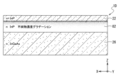
- FIG. 12 is a cross-sectional view of a photodetector 1D according to the fourth embodiment of the present disclosure.
- the same reference numerals are given to the same parts as in FIG. 8, and detailed description thereof will be omitted.
- the impurity concentration of the second compound semiconductor layer 82 is lower than that of the recombination prevention layer 22 and higher than that of the photoelectric conversion layer 26, and the impurity concentration is gradually reduced toward the photoelectric conversion layer 26 side.
- FIG. 13 is a cross-sectional view of a photodetector 1E according to the fifth embodiment of the present disclosure.
- the same parts as in FIG. 4 are denoted by the same reference numerals, and detailed description thereof will be omitted.
- a transparent electrode 91 is arranged on the light incident side of the recombination prevention layer 22 .
- a passivation layer 92 is arranged on the light incident side of the transparent electrode 91 .
- the transparent electrode 91 is in contact with and electrically connected to the recombination prevention layer 22 .
- a predetermined bias voltage Va is applied to the transparent electrode 91 .
- a material such as ITO (Indium Tin Oxide) that can transmit the infrared light 61 and the visible light 62 can be used.
- the passivation layer 92 a material that can transmit the infrared light 61 and the visible light 62, such as silicon oxide ( SiO2 ), silicon nitride (SiN), and aluminum oxide ( Al2O3 ) can be used.
- the passivation layer 92 may also function as an electrode and a predetermined bias voltage Va may be applied.
- FIG. 14A is a cross-sectional view of a photodetector 1E according to the sixth embodiment of the present disclosure.
- FIG. 13 the same parts as in FIG. 4 are denoted by the same reference numerals, and detailed description thereof will be omitted.
- 14B is a schematic plan view showing an arrangement pattern of pixels 3b for infrared light 61 and pixels 3a for infrared light 61 and visible light 62.
- the photodetector 1F is provided on the light incident side of the second compound semiconductor layer 23, and includes a first light transmitting portion 51 that can transmit infrared light 61 and visible light 62, and a light transmitting portion 51 that transmits infrared light 61 and visible light. It has a recombination prevention layer 93 forming a second light transmission portion 52 that blocks transmission of the light 62 .
- the film thickness of the recombination prevention layer 93 in the second light transmitting portion 52 is desirably 1 ⁇ m or more.
- the pixels 3a including the first light-transmitting portions 51 and the pixels 3b including the second light-transmitting portions 52 are alternately arranged in the X direction and the Y direction, which are orthogonal to each other in plan view. placed repeatedly.
- a pixel signal obtained by photoelectrically converting the infrared light 61 is obtained.
- a pixel signal of visible light 62 is obtained by subtracting the pixel signal of pixel 3b (infrared light 61) from the pixel signal of pixel 3a (infrared light 61+visible light 62). Therefore, according to the photodetector 1F according to the sixth embodiment, pixel signals for two wavelengths of the infrared light 61 and the visible light 62 can be obtained simultaneously with one device.
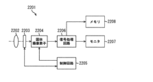
- FIG. 15 is a block diagram showing a configuration example of an imaging device as an electronic device to which the present technology is applied.
- An imaging device 2201 shown in FIG. 15 comprises an optical system 2202, a shutter device 2203, a solid-state imaging device 2204 as a photodetector, a control circuit 2205, a signal processing circuit 2206, a monitor 2207, and two memories 2208. Still images and moving images can be captured.
- the optical system 2202 has one or more lenses, guides the light (incident light) from the subject to the solid-state imaging device 2204, and forms an image on the light-receiving surface of the solid-state imaging device 2204.
- FIG. The shutter device 2203 is arranged between the optical system 2202 and the solid-state image sensor 2204 and controls the light irradiation period and the light shielding period for the solid-state image sensor 2204 according to the control of the control circuit 2205 .
- the solid-state imaging device 2204 is composed of a package including the above-described solid-state imaging device.
- the solid-state imaging device 2204 accumulates signal charges for a certain period of time according to the light imaged on the light receiving surface via the optical system 2202 and the shutter device 2203 .
- the signal charges accumulated in the solid-state imaging device 2204 are transferred according to the drive signal (timing signal) supplied from the control circuit 2205 .
- the control circuit 2205 drives the solid-state image sensor 2204 and the shutter device 2203 by outputting drive signals for controlling the transfer operation of the solid-state image sensor 2204 and the shutter operation of the shutter device 2203 .
- a signal processing circuit 2206 performs various signal processing on the signal charges output from the solid-state imaging device 2204 .
- An image (image data) obtained by the signal processing performed by the signal processing circuit 2206 is supplied to the monitor 2207 to be displayed, or supplied to the memory 2208 to be stored (recorded). Also in the imaging device 2201 configured in this way, the photodetectors 1A, 1B, 1C, 1D, 1E, and 1F can be applied in place of the solid-state imaging device 2204 described above.
- the technology (the present technology) according to the present disclosure can be applied to various products.
- the technology according to the present disclosure can be realized as a device mounted on any type of moving body such as automobiles, electric vehicles, hybrid electric vehicles, motorcycles, bicycles, personal mobility, airplanes, drones, ships, and robots. may
- FIG. 16 is a block diagram showing a schematic configuration example of a vehicle control system, which is an example of a mobile control system to which the technology according to the present disclosure can be applied.
- Vehicle control system 12000 comprises a plurality of electronic control units connected via communication network 12001 .
- the vehicle control system 12000 includes a drive train control unit 12010, a body system control unit 12020, an outside information detection unit 12030, an inside information detection unit 12040, and an integrated control unit 12050.
- a microcomputer 12051, an audio/image output unit 12052, and an in-vehicle network I/F (interface) 12053 are illustrated.
- the drive system control unit 12010 controls the operation of devices related to the drive system of the vehicle according to various programs.
- the driving system control unit 12010 includes a driving force generator for generating driving force of the vehicle such as an internal combustion engine or a driving motor, a driving force transmission mechanism for transmitting the driving force to the wheels, and a steering angle of the vehicle. It functions as a control device such as a steering mechanism to adjust and a brake device to generate braking force of the vehicle.
- the body system control unit 12020 controls the operation of various devices equipped on the vehicle body according to various programs.
- the body system control unit 12020 functions as a keyless entry system, a smart key system, a power window device, or a control device for various lamps such as headlamps, back lamps, brake lamps, winkers or fog lamps.
- body system control unit 12020 can receive radio waves transmitted from a portable device that substitutes for a key or signals from various switches.
- the body system control unit 12020 receives the input of these radio waves or signals and controls the door lock device, power window device, lamps, etc. of the vehicle.
- the vehicle exterior information detection unit 12030 detects information outside the vehicle in which the vehicle control system 12000 is installed.
- the vehicle exterior information detection unit 12030 is connected with an imaging section 12031 .
- the vehicle exterior information detection unit 12030 causes the imaging unit 12031 to capture an image of the exterior of the vehicle, and receives the captured image.
- the vehicle exterior information detection unit 12030 may perform object detection processing or distance detection processing such as people, vehicles, obstacles, signs, or characters on the road surface based on the received image.
- the imaging unit 12031 is an optical sensor that receives light and outputs an electrical signal according to the amount of received light.
- the imaging unit 12031 can output the electric signal as an image, and can also output it as distance measurement information.
- the light received by the imaging unit 12031 may be visible light or non-visible light such as infrared rays.
- the in-vehicle information detection unit 12040 detects in-vehicle information.
- the in-vehicle information detection unit 12040 is connected to, for example, a driver state detection section 12041 that detects the state of the driver.
- the driver state detection unit 12041 includes, for example, a camera that captures an image of the driver, and the in-vehicle information detection unit 12040 detects the degree of fatigue or concentration of the driver based on the detection information input from the driver state detection unit 12041. It may be calculated, or it may be determined whether the driver is dozing off.
- the microcomputer 12051 calculates control target values for the driving force generator, the steering mechanism, or the braking device based on the information inside and outside the vehicle acquired by the vehicle exterior information detection unit 12030 or the vehicle interior information detection unit 12040, and controls the drive system control unit.
- a control command can be output to 12010 .
- the microcomputer 12051 realizes the functions of ADAS (Advanced Driver Assistance System) including collision avoidance or shock mitigation, follow-up driving based on inter-vehicle distance, vehicle speed maintenance driving, vehicle collision warning, or vehicle lane deviation warning. Cooperative control can be performed for the purpose of ADAS (Advanced Driver Assistance System) including collision avoidance or shock mitigation, follow-up driving based on inter-vehicle distance, vehicle speed maintenance driving, vehicle collision warning, or vehicle lane deviation warning. Cooperative control can be performed for the purpose of ADAS (Advanced Driver Assistance System) including collision avoidance or shock mitigation, follow-up driving based on inter-vehicle distance, vehicle speed maintenance driving, vehicle collision warning, or vehicle
- the microcomputer 12051 controls the driving force generator, the steering mechanism, the braking device, etc. based on the information about the vehicle surroundings acquired by the vehicle exterior information detection unit 12030 or the vehicle interior information detection unit 12040, so that the driver's Cooperative control can be performed for the purpose of autonomous driving, etc., in which vehicles autonomously travel without depending on operation.
- the microcomputer 12051 can output a control command to the body system control unit 12020 based on the information outside the vehicle acquired by the information detection unit 12030 outside the vehicle.
- the microcomputer 12051 controls the headlamps according to the position of the preceding vehicle or the oncoming vehicle detected by the vehicle exterior information detection unit 12030, and performs cooperative control aimed at anti-glare such as switching from high beam to low beam. It can be carried out.
- the audio/image output unit 12052 transmits at least one of audio and/or image output signals to an output device capable of visually or audibly notifying the passengers of the vehicle or the outside of the vehicle.
- an audio speaker 12061, a display unit 12062, and an instrument panel 12063 are illustrated as output devices.
- the display unit 12062 may include at least one of an on-board display and a head-up display, for example.
- FIG. 17 is a diagram showing an example of the installation position of the imaging unit 12031.
- vehicle 12100 has imaging units 12101 , 12102 , 12103 , 12104 , and 12105 as imaging unit 12031 .
- the imaging units 12101, 12102, 12103, 12104, and 12105 are provided at positions such as the front nose of the vehicle 12100, the side mirrors, the rear bumper, the back door, and the upper part of the windshield in the vehicle interior, for example.
- An image pickup unit 12101 provided in the front nose and an image pickup unit 12105 provided above the windshield in the passenger compartment mainly acquire images in front of the vehicle 12100 .
- Imaging units 12102 and 12103 provided in the side mirrors mainly acquire side images of the vehicle 12100 .
- An imaging unit 12104 provided in the rear bumper or back door mainly acquires an image behind the vehicle 12100 .
- Forward images acquired by the imaging units 12101 and 12105 are mainly used for detecting preceding vehicles, pedestrians, obstacles, traffic lights, traffic signs, lanes, and the like.
- FIG. 17 shows an example of the imaging range of the imaging units 12101 to 12104.
- the imaging range 12111 indicates the imaging range of the imaging unit 12101 provided in the front nose
- the imaging ranges 12112 and 12113 indicate the imaging ranges of the imaging units 12102 and 12103 provided in the side mirrors, respectively
- the imaging range 12114 The imaging range of an imaging unit 12104 provided in the rear bumper or back door is shown. For example, by superimposing the image data captured by the imaging units 12101 to 12104, a bird's-eye view image of the vehicle 12100 viewed from above can be obtained.
- At least one of the imaging units 12101 to 12104 may have a function of acquiring distance information.
- at least one of the imaging units 12101 to 12104 may be a stereo camera composed of a plurality of imaging elements, or may be an imaging element having pixels for phase difference detection.
- the microcomputer 12051 determines the distance to each three-dimensional object within the imaging ranges 12111 to 12114 and changes in this distance over time (relative velocity with respect to the vehicle 12100). , it is possible to extract, as the preceding vehicle, the closest three-dimensional object on the course of the vehicle 12100, which runs at a predetermined speed (for example, 0 km/h or more) in substantially the same direction as the vehicle 12100. can. Furthermore, the microcomputer 12051 can set the inter-vehicle distance to be secured in advance in front of the preceding vehicle, and perform automatic brake control (including following stop control) and automatic acceleration control (including following start control). In this way, cooperative control can be performed for the purpose of automatic driving in which the vehicle runs autonomously without relying on the operation of the driver.
- automatic brake control including following stop control
- automatic acceleration control including following start control
- the microcomputer 12051 converts three-dimensional object data related to three-dimensional objects to other three-dimensional objects such as motorcycles, ordinary vehicles, large vehicles, pedestrians, and utility poles. It can be classified and extracted and used for automatic avoidance of obstacles. For example, the microcomputer 12051 distinguishes obstacles around the vehicle 12100 into those that are visible to the driver of the vehicle 12100 and those that are difficult to see. Then, the microcomputer 12051 judges the collision risk indicating the degree of danger of collision with each obstacle, and when the collision risk is equal to or higher than the set value and there is a possibility of collision, an audio speaker 12061 and a display unit 12062 are displayed. By outputting an alarm to the driver via the drive system control unit 12010 and performing forced deceleration and avoidance steering via the drive system control unit 12010, driving support for collision avoidance can be performed.
- At least one of the imaging units 12101 to 12104 may be an infrared camera that detects infrared rays.
- the microcomputer 12051 can recognize a pedestrian by determining whether or not the pedestrian exists in the captured images of the imaging units 12101 to 12104 .
- recognition of a pedestrian is performed by, for example, a procedure for extracting feature points in images captured by the imaging units 12101 to 12104 as infrared cameras, and performing pattern matching processing on a series of feature points indicating the outline of an object to determine whether or not the pedestrian is a pedestrian.
- the audio image output unit 12052 outputs a rectangular outline for emphasis to the recognized pedestrian. is superimposed on the display unit 12062 . Also, the audio/image output unit 12052 may control the display unit 12062 to display an icon or the like indicating a pedestrian at a desired position.
- the technology according to the present disclosure can be applied to, for example, the imaging unit 12031 among the configurations described above.
- the photodetector 1A in FIG. 1, the photodetector 1B in FIG. 10, the photodetector 1C in FIG. 11, the photodetector 1D in FIG. 12, the photodetector 1E in FIG. 13, and the photodetector in FIG. 14A Apparatus 1F can be applied.
- the pixel area is a light transmission layer made of a first compound semiconductor and transmitting incident infrared light;
- a photoelectric device that is laminated on the surface of the light transmission layer opposite to the light incident surface, is made of a second compound semiconductor different from the first compound semiconductor, and photoelectrically converts infrared light that has passed through the light transmission layer.
- the light transmission layer is a first semiconductor layer provided on the light incident surface side and having a thickness capable of transmitting the visible light;
- the photodetector according to (1) further comprising a passivation layer disposed on the light incident surface side of the light transmission layer and transmitting the infrared light and the visible light.
- the photodetector according to (1) above which is disposed on the light incident surface side of the light transmission layer and has a transparent electrode and a passivation layer that transmit the infrared light and the visible light.
- the second semiconductor layer is configured by stacking a plurality of layers, The impurity concentration of the first stage positioned closer to the photoelectric conversion layer among the plurality of stages is lower than the impurity concentration of the second stage stacked closer to the light incident surface than the first stage. photodetector.
- the first semiconductor layer has a thickness of 5 ⁇ 10 17 cm ⁇ 3 or more and 30 nm or less.
- the pixel area is a light transmission layer made of a first compound semiconductor and transmitting incident infrared light;
- a photoelectric device that is laminated on the surface of the light transmission layer opposite to the light incident surface, is made of a second compound semiconductor different from the first compound semiconductor, and photoelectrically converts infrared light that has passed through the light transmission layer.
- the light transmission layer is a first semiconductor layer provided on the light incident surface side and having a thickness capable of transmitting the visible light;
- a second semiconductor layer laminated on the surface opposite to the light incident surface of the first semiconductor layer and photoelectrically converting visible light transmitted through the first semiconductor layer,
- the second semiconductor layer has a lower impurity concentration than the first semiconductor layer and a photodetector device having a higher impurity concentration than the photoelectric conversion layer, Electronics.
- Photodetector 2 Semiconductor chip 2A Pixel region 2B Peripheral regions 3, 3a, 3b Pixel 4 Vertical drive circuit 5 Column signal processing circuit 6 Horizontal drive circuit 7 Output circuit 8 Control circuit 10 Pixel Drive wiring 11 Vertical signal wiring 12 Horizontal signal wiring 13 Logic circuit 14 Bonding pad (input/output terminal) 15 readout circuit 20 photoelectric conversion substrate 22, 73, 93 recombination prevention layers 23, 72, 81, 82 second compound semiconductor layers 23x, 25x first surfaces 23y, 25y second surface 25 first compound semiconductor layer 26 , 71 photoelectric conversion layer 27 cap layer 28 contact region 29 protective film 29a openings 31, 41 connection electrode 40 circuit board portion 42 bump electrode 43 insulating layer 51 first light transmitting portion 52 second light transmitting portion 57 microlens ( on-chip lens) 61 Infrared light 62 Visible light 91 Transparent electrode 92 Passivation layer 811 First step layer 812 Second step layer 2201 Imaging device 2202 Optical system 2
Landscapes
- Light Receiving Elements (AREA)
Priority Applications (2)
| Application Number | Priority Date | Filing Date | Title |
|---|---|---|---|
| PCT/JP2021/048832 WO2023127110A1 (ja) | 2021-12-28 | 2021-12-28 | 光検出装置及び電子機器 |
| JP2023570590A JPWO2023127110A1 (https=) | 2021-12-28 | 2021-12-28 |
Applications Claiming Priority (1)
| Application Number | Priority Date | Filing Date | Title |
|---|---|---|---|
| PCT/JP2021/048832 WO2023127110A1 (ja) | 2021-12-28 | 2021-12-28 | 光検出装置及び電子機器 |
Publications (1)
| Publication Number | Publication Date |
|---|---|
| WO2023127110A1 true WO2023127110A1 (ja) | 2023-07-06 |
Family
ID=86998388
Family Applications (1)
| Application Number | Title | Priority Date | Filing Date |
|---|---|---|---|
| PCT/JP2021/048832 Ceased WO2023127110A1 (ja) | 2021-12-28 | 2021-12-28 | 光検出装置及び電子機器 |
Country Status (2)
| Country | Link |
|---|---|
| JP (1) | JPWO2023127110A1 (https=) |
| WO (1) | WO2023127110A1 (https=) |
Citations (6)
| Publication number | Priority date | Publication date | Assignee | Title |
|---|---|---|---|---|
| JPH03104287A (ja) * | 1989-09-19 | 1991-05-01 | Fujitsu Ltd | 半導体受光素子の製造方法 |
| JP2003234494A (ja) * | 2002-02-08 | 2003-08-22 | Sumitomo Electric Ind Ltd | 半導体受光素子 |
| JP2013258328A (ja) * | 2012-06-13 | 2013-12-26 | Sumitomo Electric Ind Ltd | 受光素子および光学装置 |
| JP2015149422A (ja) * | 2014-02-07 | 2015-08-20 | ソニー株式会社 | 受光素子、撮像素子及び撮像装置 |
| JP2015220463A (ja) * | 2014-05-14 | 2015-12-07 | 三星電子株式会社Samsung Electronics Co.,Ltd. | 横型フォトダイオード、及びそれを含むイメージセンサ、並びにフォトダイオード及びイメージセンサの製造方法 |
| JP2018190798A (ja) * | 2017-04-28 | 2018-11-29 | 住友電気工業株式会社 | 赤外線検知半導体デバイス |
-
2021
- 2021-12-28 JP JP2023570590A patent/JPWO2023127110A1/ja not_active Abandoned
- 2021-12-28 WO PCT/JP2021/048832 patent/WO2023127110A1/ja not_active Ceased
Patent Citations (6)
| Publication number | Priority date | Publication date | Assignee | Title |
|---|---|---|---|---|
| JPH03104287A (ja) * | 1989-09-19 | 1991-05-01 | Fujitsu Ltd | 半導体受光素子の製造方法 |
| JP2003234494A (ja) * | 2002-02-08 | 2003-08-22 | Sumitomo Electric Ind Ltd | 半導体受光素子 |
| JP2013258328A (ja) * | 2012-06-13 | 2013-12-26 | Sumitomo Electric Ind Ltd | 受光素子および光学装置 |
| JP2015149422A (ja) * | 2014-02-07 | 2015-08-20 | ソニー株式会社 | 受光素子、撮像素子及び撮像装置 |
| JP2015220463A (ja) * | 2014-05-14 | 2015-12-07 | 三星電子株式会社Samsung Electronics Co.,Ltd. | 横型フォトダイオード、及びそれを含むイメージセンサ、並びにフォトダイオード及びイメージセンサの製造方法 |
| JP2018190798A (ja) * | 2017-04-28 | 2018-11-29 | 住友電気工業株式会社 | 赤外線検知半導体デバイス |
Also Published As
| Publication number | Publication date |
|---|---|
| JPWO2023127110A1 (https=) | 2023-07-06 |
Similar Documents
| Publication | Publication Date | Title |
|---|---|---|
| CN111226318B (zh) | 摄像器件和电子设备 | |
| US12349487B2 (en) | Solid-state image pickup device and electronic apparatus | |
| US20230261029A1 (en) | Light-receiving element and manufacturing method thereof, and electronic device | |
| TWI731035B (zh) | 光電轉換元件及光電轉換裝置 | |
| US12272711B2 (en) | Solid-state imaging device and imaging device | |
| WO2018088083A1 (ja) | 受光素子、受光素子の製造方法および電子機器 | |
| US11456323B2 (en) | Imaging unit | |
| WO2022113757A1 (ja) | 固体撮像装置及びその製造方法 | |
| JP2023150251A (ja) | 光検出装置及び電子機器 | |
| KR102786633B1 (ko) | 촬상 장치 | |
| US20250063839A1 (en) | Imaging device and electronic device | |
| TW202416726A (zh) | 光檢測裝置及電子機器 | |
| CN118891732A (zh) | 光检测装置和测距装置 | |
| WO2023127110A1 (ja) | 光検出装置及び電子機器 | |
| WO2022270023A1 (ja) | 光検出器及び電子機器 | |
| WO2022244384A1 (ja) | 光検出装置および測距装置 | |
| JP2024041483A (ja) | 光検出装置、光検出装置の製造方法、及び電子機器 | |
| WO2022181536A1 (ja) | 光検出装置及び電子機器 | |
| WO2020149181A1 (ja) | 撮像装置 | |
| WO2024090095A1 (en) | Photodetection device and electronic equipment | |
| JP7835696B2 (ja) | 光検出装置および測距装置 | |
| US20250227390A1 (en) | Linear sensor | |
| WO2025062845A1 (ja) | 光検出装置、電子機器及び光検出装置の製造方法 | |
| WO2023100547A1 (ja) | 撮像装置および電子機器 | |
| US20240290809A1 (en) | Solid-state image sensor, manufacturing method thereof, and electronic device |
Legal Events
| Date | Code | Title | Description |
|---|---|---|---|
| 121 | Ep: the epo has been informed by wipo that ep was designated in this application |
Ref document number: 21969991 Country of ref document: EP Kind code of ref document: A1 |
|
| ENP | Entry into the national phase |
Ref document number: 2023570590 Country of ref document: JP Kind code of ref document: A |
|
| WWE | Wipo information: entry into national phase |
Ref document number: 18721729 Country of ref document: US |
|
| NENP | Non-entry into the national phase |
Ref country code: DE |
|
| 122 | Ep: pct application non-entry in european phase |
Ref document number: 21969991 Country of ref document: EP Kind code of ref document: A1 |