WO2023127110A1 - 光検出装置及び電子機器 - Google Patents
光検出装置及び電子機器 Download PDFInfo
- Publication number
- WO2023127110A1 WO2023127110A1 PCT/JP2021/048832 JP2021048832W WO2023127110A1 WO 2023127110 A1 WO2023127110 A1 WO 2023127110A1 JP 2021048832 W JP2021048832 W JP 2021048832W WO 2023127110 A1 WO2023127110 A1 WO 2023127110A1
- Authority
- WO
- WIPO (PCT)
- Prior art keywords
- light
- layer
- semiconductor layer
- photoelectric conversion
- photodetector
- Prior art date
Links
- 239000004065 semiconductor Substances 0.000 claims abstract description 154
- 238000006243 chemical reaction Methods 0.000 claims abstract description 98
- 150000001875 compounds Chemical class 0.000 claims abstract description 83
- 230000005540 biological transmission Effects 0.000 claims abstract description 50
- 239000012535 impurity Substances 0.000 claims abstract description 49
- 239000011159 matrix material Substances 0.000 claims abstract description 9
- 229910000530 Gallium indium arsenide Inorganic materials 0.000 claims description 18
- 238000000034 method Methods 0.000 claims description 15
- 238000002161 passivation Methods 0.000 claims description 11
- 229910052710 silicon Inorganic materials 0.000 claims description 8
- 229910052782 aluminium Inorganic materials 0.000 claims description 4
- 229910052725 zinc Inorganic materials 0.000 claims description 4
- 229910052793 cadmium Inorganic materials 0.000 claims description 3
- 229910052749 magnesium Inorganic materials 0.000 claims description 3
- 229910052717 sulfur Inorganic materials 0.000 claims description 3
- 206010034960 Photophobia Diseases 0.000 abstract description 8
- 208000013469 light sensitivity Diseases 0.000 abstract description 8
- 230000007547 defect Effects 0.000 abstract description 7
- 239000013078 crystal Substances 0.000 abstract description 5
- 230000004044 response Effects 0.000 abstract description 3
- 238000003384 imaging method Methods 0.000 description 59
- 230000002265 prevention Effects 0.000 description 45
- 230000006798 recombination Effects 0.000 description 45
- 238000005215 recombination Methods 0.000 description 45
- 238000012545 processing Methods 0.000 description 28
- 238000001514 detection method Methods 0.000 description 26
- GPXJNWSHGFTCBW-UHFFFAOYSA-N Indium phosphide Chemical compound [In]#P GPXJNWSHGFTCBW-UHFFFAOYSA-N 0.000 description 18
- 238000010586 diagram Methods 0.000 description 16
- 239000000758 substrate Substances 0.000 description 14
- 230000006870 function Effects 0.000 description 12
- 239000000463 material Substances 0.000 description 12
- 238000005516 engineering process Methods 0.000 description 11
- 230000001681 protective effect Effects 0.000 description 10
- 230000008569 process Effects 0.000 description 9
- VYPSYNLAJGMNEJ-UHFFFAOYSA-N Silicium dioxide Chemical compound O=[Si]=O VYPSYNLAJGMNEJ-UHFFFAOYSA-N 0.000 description 8
- 230000000694 effects Effects 0.000 description 8
- 230000003287 optical effect Effects 0.000 description 8
- 229910052581 Si3N4 Inorganic materials 0.000 description 7
- HQVNEWCFYHHQES-UHFFFAOYSA-N silicon nitride Chemical compound N12[Si]34N5[Si]62N3[Si]51N64 HQVNEWCFYHHQES-UHFFFAOYSA-N 0.000 description 7
- XUIMIQQOPSSXEZ-UHFFFAOYSA-N Silicon Chemical compound [Si] XUIMIQQOPSSXEZ-UHFFFAOYSA-N 0.000 description 6
- 239000000969 carrier Substances 0.000 description 6
- 239000010703 silicon Substances 0.000 description 6
- 229910052814 silicon oxide Inorganic materials 0.000 description 6
- 230000000052 comparative effect Effects 0.000 description 5
- 230000000875 corresponding effect Effects 0.000 description 5
- 239000011701 zinc Substances 0.000 description 5
- 230000003321 amplification Effects 0.000 description 4
- 230000007246 mechanism Effects 0.000 description 4
- 238000003199 nucleic acid amplification method Methods 0.000 description 4
- TWNQGVIAIRXVLR-UHFFFAOYSA-N oxo(oxoalumanyloxy)alumane Chemical compound O=[Al]O[Al]=O TWNQGVIAIRXVLR-UHFFFAOYSA-N 0.000 description 4
- 238000002834 transmittance Methods 0.000 description 4
- PXHVJJICTQNCMI-UHFFFAOYSA-N Nickel Chemical compound [Ni] PXHVJJICTQNCMI-UHFFFAOYSA-N 0.000 description 3
- KDLHZDBZIXYQEI-UHFFFAOYSA-N Palladium Chemical compound [Pd] KDLHZDBZIXYQEI-UHFFFAOYSA-N 0.000 description 3
- 241000519995 Stachys sylvatica Species 0.000 description 3
- 230000009471 action Effects 0.000 description 3
- 239000011777 magnesium Substances 0.000 description 3
- 230000015654 memory Effects 0.000 description 3
- 230000002093 peripheral effect Effects 0.000 description 3
- BASFCYQUMIYNBI-UHFFFAOYSA-N platinum Chemical compound [Pt] BASFCYQUMIYNBI-UHFFFAOYSA-N 0.000 description 3
- 239000010936 titanium Substances 0.000 description 3
- RTAQQCXQSZGOHL-UHFFFAOYSA-N Titanium Chemical compound [Ti] RTAQQCXQSZGOHL-UHFFFAOYSA-N 0.000 description 2
- HCHKCACWOHOZIP-UHFFFAOYSA-N Zinc Chemical compound [Zn] HCHKCACWOHOZIP-UHFFFAOYSA-N 0.000 description 2
- XAGFODPZIPBFFR-UHFFFAOYSA-N aluminium Chemical compound [Al] XAGFODPZIPBFFR-UHFFFAOYSA-N 0.000 description 2
- 238000004891 communication Methods 0.000 description 2
- 230000003247 decreasing effect Effects 0.000 description 2
- 239000010931 gold Substances 0.000 description 2
- 238000009434 installation Methods 0.000 description 2
- 229910052719 titanium Inorganic materials 0.000 description 2
- 238000012546 transfer Methods 0.000 description 2
- WFKWXMTUELFFGS-UHFFFAOYSA-N tungsten Chemical compound [W] WFKWXMTUELFFGS-UHFFFAOYSA-N 0.000 description 2
- 229910052721 tungsten Inorganic materials 0.000 description 2
- 239000010937 tungsten Substances 0.000 description 2
- OKTJSMMVPCPJKN-UHFFFAOYSA-N Carbon Chemical compound [C] OKTJSMMVPCPJKN-UHFFFAOYSA-N 0.000 description 1
- 208000032544 Cicatrix Diseases 0.000 description 1
- 229940126062 Compound A Drugs 0.000 description 1
- NLDMNSXOCDLTTB-UHFFFAOYSA-N Heterophylliin A Natural products O1C2COC(=O)C3=CC(O)=C(O)C(O)=C3C3=C(O)C(O)=C(O)C=C3C(=O)OC2C(OC(=O)C=2C=C(O)C(O)=C(O)C=2)C(O)C1OC(=O)C1=CC(O)=C(O)C(O)=C1 NLDMNSXOCDLTTB-UHFFFAOYSA-N 0.000 description 1
- FYYHWMGAXLPEAU-UHFFFAOYSA-N Magnesium Chemical compound [Mg] FYYHWMGAXLPEAU-UHFFFAOYSA-N 0.000 description 1
- 240000004050 Pentaglottis sempervirens Species 0.000 description 1
- 235000004522 Pentaglottis sempervirens Nutrition 0.000 description 1
- 206010034972 Photosensitivity reaction Diseases 0.000 description 1
- NINIDFKCEFEMDL-UHFFFAOYSA-N Sulfur Chemical compound [S] NINIDFKCEFEMDL-UHFFFAOYSA-N 0.000 description 1
- NRTOMJZYCJJWKI-UHFFFAOYSA-N Titanium nitride Chemical compound [Ti]#N NRTOMJZYCJJWKI-UHFFFAOYSA-N 0.000 description 1
- KXNLCSXBJCPWGL-UHFFFAOYSA-N [Ga].[As].[In] Chemical compound [Ga].[As].[In] KXNLCSXBJCPWGL-UHFFFAOYSA-N 0.000 description 1
- 230000001133 acceleration Effects 0.000 description 1
- 229910045601 alloy Inorganic materials 0.000 description 1
- 239000000956 alloy Substances 0.000 description 1
- 230000002768 anti-recombination Effects 0.000 description 1
- 230000003139 buffering effect Effects 0.000 description 1
- BDOSMKKIYDKNTQ-UHFFFAOYSA-N cadmium atom Chemical compound [Cd] BDOSMKKIYDKNTQ-UHFFFAOYSA-N 0.000 description 1
- 229910052799 carbon Inorganic materials 0.000 description 1
- 229910052681 coesite Inorganic materials 0.000 description 1
- 238000002485 combustion reaction Methods 0.000 description 1
- 230000000295 complement effect Effects 0.000 description 1
- 239000000470 constituent Substances 0.000 description 1
- 230000001276 controlling effect Effects 0.000 description 1
- 238000012937 correction Methods 0.000 description 1
- 230000002596 correlated effect Effects 0.000 description 1
- 229910052906 cristobalite Inorganic materials 0.000 description 1
- 238000009792 diffusion process Methods 0.000 description 1
- 230000001747 exhibiting effect Effects 0.000 description 1
- 230000005669 field effect Effects 0.000 description 1
- VTGARNNDLOTBET-UHFFFAOYSA-N gallium antimonide Chemical compound [Sb]#[Ga] VTGARNNDLOTBET-UHFFFAOYSA-N 0.000 description 1
- 229910052732 germanium Inorganic materials 0.000 description 1
- GNPVGFCGXDBREM-UHFFFAOYSA-N germanium atom Chemical compound [Ge] GNPVGFCGXDBREM-UHFFFAOYSA-N 0.000 description 1
- PCHJSUWPFVWCPO-UHFFFAOYSA-N gold Chemical compound [Au] PCHJSUWPFVWCPO-UHFFFAOYSA-N 0.000 description 1
- 229910052737 gold Inorganic materials 0.000 description 1
- 229910052738 indium Inorganic materials 0.000 description 1
- APFVFJFRJDLVQX-UHFFFAOYSA-N indium atom Chemical compound [In] APFVFJFRJDLVQX-UHFFFAOYSA-N 0.000 description 1
- AMGQUBHHOARCQH-UHFFFAOYSA-N indium;oxotin Chemical compound [In].[Sn]=O AMGQUBHHOARCQH-UHFFFAOYSA-N 0.000 description 1
- 239000011810 insulating material Substances 0.000 description 1
- 239000012212 insulator Substances 0.000 description 1
- 238000010030 laminating Methods 0.000 description 1
- 238000012423 maintenance Methods 0.000 description 1
- 238000004519 manufacturing process Methods 0.000 description 1
- 238000005259 measurement Methods 0.000 description 1
- 229910052751 metal Inorganic materials 0.000 description 1
- 239000002184 metal Substances 0.000 description 1
- 229910044991 metal oxide Inorganic materials 0.000 description 1
- 150000004706 metal oxides Chemical class 0.000 description 1
- 230000000116 mitigating effect Effects 0.000 description 1
- 238000012986 modification Methods 0.000 description 1
- 230000004048 modification Effects 0.000 description 1
- 229910021421 monocrystalline silicon Inorganic materials 0.000 description 1
- 229910052759 nickel Inorganic materials 0.000 description 1
- 230000001151 other effect Effects 0.000 description 1
- 229910052763 palladium Inorganic materials 0.000 description 1
- 230000036211 photosensitivity Effects 0.000 description 1
- 229910052697 platinum Inorganic materials 0.000 description 1
- 239000011347 resin Substances 0.000 description 1
- 229920005989 resin Polymers 0.000 description 1
- 238000005070 sampling Methods 0.000 description 1
- 231100000241 scar Toxicity 0.000 description 1
- 230000037387 scars Effects 0.000 description 1
- 230000035939 shock Effects 0.000 description 1
- HBMJWWWQQXIZIP-UHFFFAOYSA-N silicon carbide Chemical compound [Si+]#[C-] HBMJWWWQQXIZIP-UHFFFAOYSA-N 0.000 description 1
- 239000000377 silicon dioxide Substances 0.000 description 1
- 235000012239 silicon dioxide Nutrition 0.000 description 1
- 229910052682 stishovite Inorganic materials 0.000 description 1
- 239000011593 sulfur Substances 0.000 description 1
- JBQYATWDVHIOAR-UHFFFAOYSA-N tellanylidenegermanium Chemical compound [Te]=[Ge] JBQYATWDVHIOAR-UHFFFAOYSA-N 0.000 description 1
- 229910052905 tridymite Inorganic materials 0.000 description 1
Images


Classifications
-
- H—ELECTRICITY
- H01—ELECTRIC ELEMENTS
- H01L—SEMICONDUCTOR DEVICES NOT COVERED BY CLASS H10
- H01L27/00—Devices consisting of a plurality of semiconductor or other solid-state components formed in or on a common substrate
- H01L27/14—Devices consisting of a plurality of semiconductor or other solid-state components formed in or on a common substrate including semiconductor components sensitive to infrared radiation, light, electromagnetic radiation of shorter wavelength or corpuscular radiation and specially adapted either for the conversion of the energy of such radiation into electrical energy or for the control of electrical energy by such radiation
- H01L27/144—Devices controlled by radiation
- H01L27/146—Imager structures
-
- H—ELECTRICITY
- H01—ELECTRIC ELEMENTS
- H01L—SEMICONDUCTOR DEVICES NOT COVERED BY CLASS H10
- H01L31/00—Semiconductor devices sensitive to infrared radiation, light, electromagnetic radiation of shorter wavelength or corpuscular radiation and specially adapted either for the conversion of the energy of such radiation into electrical energy or for the control of electrical energy by such radiation; Processes or apparatus specially adapted for the manufacture or treatment thereof or of parts thereof; Details thereof
- H01L31/08—Semiconductor devices sensitive to infrared radiation, light, electromagnetic radiation of shorter wavelength or corpuscular radiation and specially adapted either for the conversion of the energy of such radiation into electrical energy or for the control of electrical energy by such radiation; Processes or apparatus specially adapted for the manufacture or treatment thereof or of parts thereof; Details thereof in which radiation controls flow of current through the device, e.g. photoresistors
- H01L31/10—Semiconductor devices sensitive to infrared radiation, light, electromagnetic radiation of shorter wavelength or corpuscular radiation and specially adapted either for the conversion of the energy of such radiation into electrical energy or for the control of electrical energy by such radiation; Processes or apparatus specially adapted for the manufacture or treatment thereof or of parts thereof; Details thereof in which radiation controls flow of current through the device, e.g. photoresistors characterised by potential barriers, e.g. phototransistors
Definitions
- the present disclosure relates to a photodetector and an electronic device equipped with this photodetector.
- an imaging element provided in an image sensor for detecting visible light such as red light (R), green light (G), and blue light (B) is usually a light receiving element formed on a silicon semiconductor substrate. It has an element (photodiode).
- R red light
- G green light
- B blue light
- IR infrared light
- InGaAs image sensors that can detect infrared light by using InGaAs instead of silicon. It is known that this InGaAs image sensor is formed by forming an InGaAs film on an InP substrate, and light is incident from the InP substrate side. However, the InGaAs image sensor cannot detect visible light unless the InP substrate on the light incident side is removed.
- Patent Document 1 there is a known method of increasing the visible light sensitivity of an InGaAs image sensor by thinning the n+InP layer (recombination prevention layer that suppresses the generation of dark current) on the light incident side.
- the damage during the process reaches the narrow bandgap InGaAs layer, causing crystal defects and white spots.
- the impurity concentration of the InP layer on the light incident side photoelectric conversion is possible in the InP layer, and visible light sensitivity does not easily decrease even if the thickness of the InP layer is increased. become white scars.
- the present disclosure has been made in view of such circumstances, and an object thereof is to provide a photodetector and an electronic device capable of making it difficult for crystal defects to occur while maintaining visible light sensitivity.
- One aspect of the present disclosure includes a pixel region in which a plurality of pixels capable of generating an electric signal in response to externally incident infrared light and visible light are arranged in a matrix, and the pixel region contains a first compound A light transmission layer made of a semiconductor and transmitting incident infrared light; and a photoelectric conversion layer that photoelectrically converts infrared light transmitted through the light transmission layer, the light transmission layer being provided on the light incident surface side and having a thickness capable of transmitting the visible light.
- the semiconductor layer 2 has an impurity concentration lower than that of the first semiconductor layer and higher than that of the photoelectric conversion layer.
- Another aspect of the present disclosure includes a pixel region in which a plurality of pixels capable of generating an electric signal in response to externally incident infrared light and visible light are arranged in a matrix, and the pixel region includes a first A light-transmitting layer made of a compound semiconductor and transmitting incident infrared light; and a second compound semiconductor different from the first compound semiconductor, laminated on a surface of the light-transmitting layer opposite to the light incident surface. and a photoelectric conversion layer that photoelectrically converts infrared light transmitted through the light transmission layer, the light transmission layer being provided on the light incident surface side and having a thickness capable of transmitting the visible light.
- the second semiconductor layer has a lower impurity concentration than the first semiconductor layer and a higher impurity concentration than the photoelectric conversion layer.
- FIG. 1 is a schematic plan layout diagram showing a configuration example of a photodetector according to a first embodiment of the present disclosure
- FIG. 1 is a block diagram showing a configuration example of a photodetector according to a first embodiment of the present disclosure
- FIG. 2 is a circuit diagram showing a configuration example of a readout circuit of the photodetector according to the first embodiment of the present disclosure
- FIG. 1 is a schematic cross-sectional view of a principal part showing a configuration example of a photodetector according to a first embodiment of the present disclosure
- FIG. FIG. 4 is a characteristic diagram showing the dependence of InP film thickness and light transmittance;
- FIG. 1 is a schematic plan layout diagram showing a configuration example of a photodetector according to a first embodiment of the present disclosure
- FIG. 1 is a block diagram showing a configuration example of a photodetector according to a first embodiment of the present disclosure
- FIG. 2 is a circuit diagram showing a configuration example
- FIG. 10 is a cross-sectional view of a photodetector showing an example of the occurrence of process damage in a comparative example
- FIG. 10 is a cross-sectional view of a photodetector showing another example of occurrence of process damage in a comparative example
- FIG. 4 is a diagram for explaining how carriers photoelectrically converted with visible light are transferred to the photoelectric conversion layer in the first embodiment of the present disclosure
- FIG. 4 is a diagram shown for explaining how process damage becomes difficult to reach a photoelectric conversion layer in the first embodiment of the present disclosure
- FIG. 4 is a cross-sectional view of a photodetector according to a second embodiment of the present disclosure
- FIG. 5 is a cross-sectional view of a photodetector according to a third embodiment of the present disclosure
- FIG. 11 is a cross-sectional view of a photodetector according to a fourth embodiment of the present disclosure
- FIG. 11 is a cross-sectional view of a photodetector according to a fifth embodiment of the present disclosure
- FIG. 11 is a cross-sectional view of a photodetector according to a sixth embodiment of the present disclosure
- FIG. 3 is a schematic plan view showing an arrangement pattern of pixels for infrared light and pixels for infrared light and visible light. It is a block diagram showing a configuration example of an electronic device to which the present technology is applied.
- 1 is a block diagram showing an example of a schematic configuration of a vehicle control system
- FIG. FIG. 4 is an explanatory diagram showing an example of installation positions of an outside information detection unit and an imaging unit;
- first conductivity type is one of p-type or n-type
- second conductivity type means one of p-type or n-type, which is different from “first conductivity type”.
- first conductivity type is one of p-type or n-type
- second conductivity type means one of p-type or n-type, which is different from “first conductivity type”.
- “+” and “-” attached to "n” and “p” refer to semiconductor regions having relatively high or low impurity densities, respectively, compared to semiconductor regions not marked with “+” and “-”. It means that it is an area. However, even if the same "n” is attached to the semiconductor region, it does not mean that the impurity density of each semiconductor region is exactly the same.
- FIG. 1 is a schematic plan layout diagram showing one configuration example of a photodetector according to the first embodiment of the present disclosure.
- a photodetector 1A according to the first embodiment of the present disclosure mainly includes a semiconductor chip 2 having a square two-dimensional planar shape when viewed in plan. That is, the photodetector 1A is mounted on the semiconductor chip 2.
- FIG. This photodetector 1A takes in incident light from a subject through an optical lens (not shown), converts the light amount of the incident light formed into an image on an imaging surface into an electric signal for each pixel, and obtains a pixel signal. Output.
- the semiconductor chip 2 on which the photodetector 1A is mounted has, in a two-dimensional plane, a rectangular pixel region 2A provided in the center and a peripheral region arranged outside the pixel region 2A so as to surround the pixel region 2A. 2B.
- the pixel area 2A is, for example, a light receiving surface that receives light condensed by an optical lens.
- a plurality of pixels 3 are arranged in a matrix on a two-dimensional plane including the X direction and the Y direction.
- the pixels 3 are repeatedly arranged in the X direction and the Y direction that are orthogonal to each other within the two-dimensional plane.
- a plurality of bonding pads (input/output terminals) 14 are arranged in the peripheral region 2B. Each of the plurality of bonding pads 14 is arranged, for example, along four sides of the two-dimensional plane of the semiconductor chip 2 . Each of the plurality of bonding pads 14 is an input/output terminal used when electrically connecting the semiconductor chip 2 to an external device.
- FIG. 2 is a block diagram showing a configuration example of the photodetector 1A.
- the semiconductor chip 2 includes a logic circuit 13 including a vertical drive circuit 4, a column signal processing circuit 5, a horizontal drive circuit 6, an output circuit 7, a control circuit 8, and the like.
- the logic circuit 13 is composed of, for example, a CMOS (Complementary MOS) circuit having an n-channel conductivity type MOSFET (Metal Oxide Semiconductor Field Effect Transistor) and a p-channel conductivity type MOSFET.
- CMOS Complementary MOS
- MOSFET Metal Oxide Semiconductor Field Effect Transistor
- the vertical driving circuit 4 is composed of, for example, a shift register.
- the vertical drive circuit 4 sequentially selects desired pixel drive wirings 10, supplies pulses for driving the pixels 3 to the selected pixel drive wirings 10, and drives the pixels 3 row by row. That is, the vertical drive circuit 4 sequentially selectively scans the pixels 3 in the pixel region 2A in the vertical direction row by row, and outputs signals from the pixels 3 based on the signal charges generated by the photoelectric conversion elements of the pixels 3 according to the amount of received light.
- a pixel signal is supplied to the column signal processing circuit 5 through the vertical signal wiring 11 .
- the column signal processing circuit 5 is arranged, for example, for each column of the pixels 3, and performs signal processing such as noise removal on the signals output from the pixels 3 of one row for each pixel column.
- the column signal processing circuit 5 performs signal processing such as CDS (Correlated Double Sampling) and AD (Analog Digital) conversion for removing pixel-specific fixed pattern noise.
- the horizontal driving circuit 6 is composed of, for example, a shift register.
- the horizontal driving circuit 6 sequentially outputs a horizontal scanning pulse to the column signal processing circuit 5 to select each of the column signal processing circuits 5 in order, and the pixels subjected to the signal processing from each of the column signal processing circuits 5 are selected.
- a signal is output to the horizontal signal wiring 12 .
- the output circuit 7 performs signal processing on the pixel signals sequentially supplied from each of the column signal processing circuits 5 through the horizontal signal wiring 12 and outputs the processed signals.
- signal processing for example, buffering, black level adjustment, column variation correction, and various digital signal processing can be used.
- the control circuit 8 generates a clock signal and a control signal that serve as references for the operation of the vertical drive circuit 4, the column signal processing circuit 5, the horizontal drive circuit 6, etc. based on the vertical synchronization signal, the horizontal synchronization signal, and the master clock signal. Generate. The control circuit 8 then outputs the generated clock signal and control signal to the vertical drive circuit 4, the column signal processing circuit 5, the horizontal drive circuit 6, and the like.
- FIG. 3 is a circuit diagram showing a configuration example of the readout circuit 15 of the photodetector 1A.
- Each pixel 3 of the plurality of pixels has a photoelectric conversion element PD.
- a readout circuit 15 is connected to the photoelectric conversion element PD of each pixel 3 .
- the photoelectric conversion element PD generates charges (signal charges) corresponding to the amount of light received.
- a predetermined bias voltage Va is applied to the cathode side of the photoelectric conversion element PD.
- the readout circuit 15 is connected to the anode side of the photoelectric conversion element PD.
- the readout circuit 15 has a capacitive element Cp as a charge storage section (charge holding section), a reset transistor RST, an amplification transistor AMP, and a selection transistor SEL.
- These transistors (RST, AMP, SEL) are composed of MOSFETs having a silicon oxide film as a gate insulating film, for example.
- these transistors (RST, AMP, SEL) may be MISFETs (Metal Insulator Semiconductor FETs) whose gate insulating film is a silicon nitride (Si3N4) film or a laminated film of silicon nitride film and silicon oxide film.
- the capacitive element Cp accumulates signal charges generated by the photoelectric conversion element PD.
- the capacitive element Cp is composed of, for example, any one of pn junction capacitance, MOS capacitance, and wiring capacitance.
- the amplification transistor AMP outputs a pixel signal corresponding to the accumulated potential of the capacitive element Cp.
- the amplification transistor AMP constitutes a load MOS as a constant current source and a source follower circuit, which are connected via the vertical signal wiring 11 .
- the source follower circuit outputs a pixel signal indicating a level corresponding to the signal charge accumulated in the capacitive element Cp from the amplification transistor AMP to the column signal processing circuit 5 via the selection transistor SEL and the vertical signal line 11 .
- the selection transistor SEL outputs the pixel signal of the pixel 3 to the column signal processing circuit 5 through the vertical signal wiring 11 when the selection signal is applied to the gate electrode and the selection transistor SEL is turned on.
- a signal line to which the selection signal is transferred and a signal line to which the reset signal is transferred correspond to the pixel drive line 10 in FIG.
- FIG. 4 is a schematic cross-sectional view of a main part showing one configuration example of the photodetector 1A.
- the semiconductor chip 2 includes a photoelectric conversion board portion 20 and a circuit board portion 40 which are laminated facing each other.
- the photoelectric conversion substrate section 20 includes the above-described pixel region 2A and the like.
- the circuit board portion 40 includes the above-described logic circuit 13, bonding pads 14, readout circuit 15, and the like.
- the photoelectric conversion substrate portion 20 is arranged on a first compound semiconductor layer 25 having a first surface 25x and a second surface 25y opposite to each other, and on the second surface 25y side of the first compound semiconductor layer 25. and a second compound semiconductor layer 23. and a recombination prevention layer 22 as a second compound semiconductor layer arranged on the second surface 23y side of the second compound semiconductor layer 23 .
- Each of the first compound semiconductor layer 25 , the second compound semiconductor layer 23 and the recombination prevention layer 22 is commonly provided for each pixel 3 .
- the above-described photoelectric conversion element PD is provided for each pixel 3 in the first compound semiconductor layer 25 .
- the recombination prevention layer 22 suppresses dark current generation.
- the first surface 25x of the first compound semiconductor layer 25 is sometimes called an element forming surface or main surface
- the second surface 25y is sometimes called a light incident surface or a rear surface
- the first surface 23x and the second surface 23y located on opposite sides of the second compound semiconductor layer 23 the first surface 23x is the main surface and the second surface 23y is the light incident surface or the rear surface. sometimes called.
- the photoelectric conversion substrate section 20 further includes a protective film 29 on the first surface 25x side of the first compound semiconductor layer 25 to cover the first surface 25x.
- the protective film 29 is provided in common for each pixel 3 .
- the photoelectric conversion substrate section 20 includes a light shielding film (not shown), an antireflection film (not shown), a planarizing film (not shown), and a light-incident surface of the recombination prevention layer 22.
- a microlens (on-chip lens) 57 is further provided.
- the recombination prevention layer 22 and the second compound semiconductor layer 23 constitute a light transmission layer that transmits light with wavelengths in the infrared region (infrared light 61) and light with wavelengths in the visible region (visible light 62).
- the first compound semiconductor layer 25 includes, for example, a photoelectric conversion layer 26 and a cap layer 27 from the first surface 25x side.
- the recombination prevention layer 22, the second compound semiconductor layer 23, the photoelectric conversion layer 26 of the first compound semiconductor layer 25, and the cap layer 27 are epitaxially grown on a growth substrate (not shown) in this order. layer. That is, in the first compound semiconductor layer 25 , the photoelectric conversion layer 26 and the cap layer 27 are covalently bonded, and the photoelectric conversion layer 26 is covalently bonded to the second compound semiconductor layer 23 .
- the cap layer 27 is, for example, commonly provided for all the pixels 3 and arranged between the protective film 29 and the photoelectric conversion layer 26 .
- a plurality of contact regions 28 made of, for example, semiconductor regions (impurity diffusion regions) are provided in the cap layer 27 .
- a compound semiconductor material having a bandgap (Eg) larger than that of the compound semiconductor material forming the photoelectric conversion layer 26 for the cap layer 27 dark current can be suppressed.
- n-type InP indium phosphide
- Each contact region 28 of the plurality of contact regions 28 is spaced apart from each other and arranged for each pixel 3 .
- Connection electrodes (element-side connection electrodes) 31 are individually connected to the respective contact regions 28 through openings 29 a provided in the protective film 29 .
- the contact region 28 is for reading signal charges generated in the photoelectric conversion layer 26 for each pixel 3, and contains, for example, p-type impurities.
- p-type impurities for example, Zn (zinc) can be used.
- Zn zinc
- the contact region 28 is configured to be thicker than the cap layer 27 and is also provided in a part of the photoelectric conversion layer 26 in the thickness direction (Z direction).
- the photoelectric conversion layer 26 between the cap layer 27 and the second compound semiconductor layer 23 is provided in common for all the pixels 3, for example.
- the photoelectric conversion layer 26 absorbs light of a predetermined wavelength, which is infrared light 61 and visible light 62 in the first embodiment, to generate signal charges, and contains, for example, n-type impurities. It is composed of a III-V group compound semiconductor material or an i-type III-V group compound semiconductor material.
- a compound semiconductor material forming the photoelectric conversion layer 26 for example, a compound semiconductor containing either InGaAs (indium gallium arsenide) or InGaAs/GaAsSb (indium gallium antimonide) can be used.
- InGaAs indium gallium arsenide
- InGaAs/GaAsSb indium gallium antimonide
- i-type InGaAs is used as the photoelectric conversion layer 26 .
- the photoelectric conversion layer 26 photoelectrically converts light with wavelengths
- the recombination prevention layer 22 and the second compound semiconductor layer 23 are provided in common for all the pixels 3 .
- the recombination prevention layer 22 and the second compound semiconductor layer 23 also function as an electrode common to each pixel 3, and among the charges generated in the photoelectric conversion layer 26, discharge the charges that are not used as signal charges (cathode). .
- a predetermined bias voltage Va is applied to the recombination prevention layer 22 and the second compound semiconductor layer 23 .
- connection electrode 31 is supplied with a voltage for reading signal charges (holes or electrons, hereinafter for the sake of convenience, signal charges are assumed to be holes) generated in the photoelectric conversion layer 26 . It is an electrode (anode) and is provided for each pixel 3 in the pixel region 2A. That is, each pixel 3 is provided with a photoelectric conversion element PD including a connection electrode 31 , a photoelectric conversion layer 26 , a recombination prevention layer 22 that also functions as an electrode, and a second compound semiconductor layer 23 .
- the connection electrode 31 functions as an anode side electrode of the photoelectric conversion element PD, and the recombination prevention layer 22 and the second compound semiconductor layer 23 function as a cathode side electrode of the photoelectric conversion element PD.
- connection electrodes 31 are made of, for example, titanium (Ti), tungsten (W), titanium nitride (TiN), platinum (Pt), gold (Au), germanium (Ge), palladium (Pd), zinc (Zn), nickel ( Ni) and aluminum (Al), or an alloy containing at least one of them.
- the connection electrode 31 may be a single film of such constituent materials, or may be a laminated film in which two or more kinds are combined.
- the connection electrode 31 is composed of a laminated film of titanium and tungsten with a film thickness of about several tens of nm to several hundreds of nm.
- the protective film 29 is provided between the first compound semiconductor layer 25 and the insulating layer 43 .
- the protective film 29 contains oxide such as silicon oxide (SiOx) or aluminum oxide (Al2O3).
- the protective film 29 may have a laminated structure in which a plurality of films are laminated.
- the protective film 29 may be made of a silicon (Si)-based insulating material such as silicon oxynitride (SiON), carbon-containing silicon oxide (SiOC), silicon nitride (SiN), and silicon carbide (SiC).
- the thickness of the protective film 29 is, for example, about several tens of nm to several hundreds of nm.
- the recombination prevention layer 22 and the second compound semiconductor layer 23 are made of an n-type compound semiconductor having a higher impurity concentration than the photoelectric conversion layer 26 of the first compound semiconductor layer 25. It also functions as an electrode.
- a compound semiconductor containing any one of InP, InGaAsP, InGaAlAs, InAlAs, InAlAsSb, and AlAsSb can be used as the material of the recombination prevention layer 22 and the second compound semiconductor layer 23 .
- InP containing n-type impurities is used as the compound semiconductor material forming the recombination prevention layer 22 and the second compound semiconductor layer 23 .
- the second compound semiconductor layer 23 and the first compound semiconductor layer 25 are made of different compound semiconductor materials.
- FIG. 5 is a characteristic diagram showing the dependence of InP film thickness and light transmittance.
- FIG. 5 shows cases where the film thickness of InP is 20 nm, 50 nm, 100 nm, 200 nm, 500 nm, and 1000 nm.
- the wavelength range of infrared light is approximately 780 nm to 1 mm.
- the wavelength range of visible light is approximately from a lower limit of 360-400 nm to an upper limit of 760-830 nm.
- the light transmittance depends on the film thickness.
- the microlens 57 is provided on the light incident surface side of the recombination prevention layer 22 .
- the microlenses 57 are provided for each pixel 3 in the pixel region 2 ⁇ /b>A and are arranged in a matrix corresponding to the arrangement of the plurality of pixels 3 .
- the microlenses 57 condense the irradiation light and allow the condensed light to enter the pixels 3 efficiently.
- the microlens 57 is made of, for example, a resin material.
- circuit board portion 40 (Circuit board portion 40) Although illustration of a specific configuration is omitted in FIG. 4, the circuit board section 40 is located on the opposite side of the semiconductor substrate made of, for example, single crystal silicon in the thickness direction (Z direction) of the semiconductor substrate. and a multilayer wiring layer arranged on the first surface side of the first surface and the second surface. Active elements and passive elements included in circuits such as the logic circuit 13 and the readout circuit 15 are provided on the semiconductor substrate of the circuit board section 40 .
- FIG. 4 illustrates the readout circuit 15 shown in FIG. 3 by omitting reference numerals.
- connection electrodes 41 are provided in the uppermost wiring layer of the circuit board portion 40 .
- the connection electrodes 41 are arranged corresponding to the connection electrodes 31 of the photoelectric conversion substrate section 20 .
- the connection electrode 41 is electrically connected to the readout circuit 15 .
- connection electrodes 41 of the circuit board section 40 are electrically and mechanically connected to the connection electrodes 31 of the photoelectric conversion board section 20 via bump electrodes 42 .
- An insulating layer 43 is provided between the circuit board section 40 and the photoelectric conversion board section 20 except for the bump electrodes 42 .
- the circuit board section 40 and the photoelectric conversion board section 20 are joined by bump electrodes 42 and insulating layers 43 .
- the photoelectric conversion element PD of the circuit board portion 40 is electrically connected to the readout circuit 15 via the connection electrode 31 , the bump electrode 42 and the connection electrode 41 on the anode side.
- the visible light sensitivity can be increased by reducing the film thickness of the recombination prevention layer 22. It reaches up to 26.
- FIG. 6 is a cross-sectional view of the photodetector 1-1 showing an example of the occurrence of process damage in the comparative example.
- the same parts as those in FIG. 4 are denoted by the same reference numerals, and detailed description thereof will be omitted.
- the damage during the process reaches the photoelectric conversion layer 26, causing crystal defects and white spots. This white spot leaves a white portion in the image when the image is created.
- FIG. 7 is a cross-sectional view of the photodetector 1-2 showing another example of the occurrence of process damage in the comparative example.
- the same parts as those in FIG. 4 are denoted by the same reference numerals, and detailed description thereof will be omitted.
- the recombination prevention layer 22 can perform photoelectric conversion. Although the photosensitivity is difficult to decrease, the carriers generated by the interface defects are also read out, resulting in white defects.
- the total thickness of the recombination prevention layer 22 and the second compound semiconductor layer 23 shown in FIG. 8 is the same as the thickness of the recombination prevention layer 22 of the previous InGaAs image sensor. By doing so, the visible light 62 is photoelectrically converted by the second compound semiconductor layer 23, so that the visible light sensitivity is increased. Further, if the recombination prevention layer 22 is made thinner even if the total InP layer is made thicker, it becomes difficult for the process damage to reach the photoelectric conversion layer 26 while maintaining the visible light sensitivity, as shown in FIG. Crystal defects in InGaAs that cause scratches are less likely to occur.
- the film thickness of the recombination prevention layer 22 is 5 ⁇ 10 17 cm ⁇ 3 or more and 30 nm or less.
- the film thickness of the second compound semiconductor layer 23 is 1 ⁇ 10 17 cm ⁇ 3 or more and 1 ⁇ 10 18 cm ⁇ 3 or less.
- the film thickness of the photoelectric conversion layer 26 is 1 ⁇ 10 17 cm ⁇ 3 or less.
- the impurity concentration of the second compound semiconductor layer 23 is lower than that of the recombination prevention layer 22 and higher than that of the photoelectric conversion layer 26 .
- Either Si (silicon) or S (sulfur) is used as the impurity of the recombination prevention layer 22 and the second compound semiconductor layer 23 in the case of n-type.
- the impurity concentration between the recombination prevention layer 22 and the photoelectric conversion layer 26 on the light incident side is lower than that of the recombination prevention layer 22 and higher than that of the photoelectric conversion layer 26 .
- the second compound semiconductor layer 23 With providing the second compound semiconductor layer 23 with a high density, the carriers of the visible light 62 photoelectrically converted in the second compound semiconductor layer 23 can be transferred to the photoelectric conversion layer 26, thereby maintaining visible light sensitivity and white light. Process damage to the photoelectric conversion layer 26 that causes scratches can be reduced.
- FIG. 10 is a cross-sectional view of a photodetector 1B according to the second embodiment of the present disclosure.
- a photoelectric conversion layer 71, a second compound semiconductor layer 72, and a recombination prevention layer 73 are laminated in this order along the thickness direction (direction indicated by arrow Z in FIG. 10).
- the film thickness of the recombination prevention layer 73 is 5 ⁇ 10 17 cm ⁇ 3 or more and 30 nm or less. Also, the film thickness of the second compound semiconductor layer 72 is 1 ⁇ 10 17 cm ⁇ 3 or more and 1 ⁇ 10 18 cm ⁇ 3 or less. The film thickness of the photoelectric conversion layer 71 is 1 ⁇ 10 17 cm ⁇ 3 or less. Furthermore, the impurity concentration of the second compound semiconductor layer 72 is lower than that of the recombination prevention layer 73 and higher than that of the photoelectric conversion layer 71 . Any one of Mg (magnesium), Cd (cadmium), Al (aluminum), and Zn (zinc) is used as impurities in the recombination prevention layer 73 and the second compound semiconductor layer 72 .
- FIG. 11 is a cross-sectional view of a photodetector 1C according to the third embodiment of the present disclosure.
- the same parts as in FIG. 8 are denoted by the same reference numerals, and detailed description thereof will be omitted.
- the second compound semiconductor layer 81 is composed of a first layer (n InP_1) 811 and a second layer (n InP_2) 812 laminated on the photoelectric conversion layer 26 side of the first layer 811 .
- the impurity concentration of the second compound semiconductor layer 81 is lower than that of the recombination prevention layer 22 and higher than that of the photoelectric conversion layer 26 , and the impurity concentration of the first layer 811 is higher than that of the second layer 812 .
- the second compound semiconductor layer 81 is composed of the first layer 811 and the second layer 812, and the impurity in the second layer 812 located on the photoelectric conversion layer 26 side is By making the concentration lower than the impurity concentration of the first layer 811 , it is possible to reduce the manufacturing cost of the photodetector 1 ⁇ /b>C and transfer the photoelectrically converted carriers of the visible light 62 to the photoelectric conversion layer 26 .
- the second compound semiconductor layer 81 can also be composed of a plurality of layers of two or more stages. In this way, by decreasing the impurity concentration step by step toward the photoelectric conversion layer 26 , more photoelectrically converted carriers of the visible light 62 can be transferred to the photoelectric conversion layer 26 .
- FIG. 12 is a cross-sectional view of a photodetector 1D according to the fourth embodiment of the present disclosure.
- the same reference numerals are given to the same parts as in FIG. 8, and detailed description thereof will be omitted.
- the impurity concentration of the second compound semiconductor layer 82 is lower than that of the recombination prevention layer 22 and higher than that of the photoelectric conversion layer 26, and the impurity concentration is gradually reduced toward the photoelectric conversion layer 26 side.
- FIG. 13 is a cross-sectional view of a photodetector 1E according to the fifth embodiment of the present disclosure.
- the same parts as in FIG. 4 are denoted by the same reference numerals, and detailed description thereof will be omitted.
- a transparent electrode 91 is arranged on the light incident side of the recombination prevention layer 22 .
- a passivation layer 92 is arranged on the light incident side of the transparent electrode 91 .
- the transparent electrode 91 is in contact with and electrically connected to the recombination prevention layer 22 .
- a predetermined bias voltage Va is applied to the transparent electrode 91 .
- a material such as ITO (Indium Tin Oxide) that can transmit the infrared light 61 and the visible light 62 can be used.
- the passivation layer 92 a material that can transmit the infrared light 61 and the visible light 62, such as silicon oxide ( SiO2 ), silicon nitride (SiN), and aluminum oxide ( Al2O3 ) can be used.
- the passivation layer 92 may also function as an electrode and a predetermined bias voltage Va may be applied.
- FIG. 14A is a cross-sectional view of a photodetector 1E according to the sixth embodiment of the present disclosure.
- FIG. 13 the same parts as in FIG. 4 are denoted by the same reference numerals, and detailed description thereof will be omitted.
- 14B is a schematic plan view showing an arrangement pattern of pixels 3b for infrared light 61 and pixels 3a for infrared light 61 and visible light 62.
- the photodetector 1F is provided on the light incident side of the second compound semiconductor layer 23, and includes a first light transmitting portion 51 that can transmit infrared light 61 and visible light 62, and a light transmitting portion 51 that transmits infrared light 61 and visible light. It has a recombination prevention layer 93 forming a second light transmission portion 52 that blocks transmission of the light 62 .
- the film thickness of the recombination prevention layer 93 in the second light transmitting portion 52 is desirably 1 ⁇ m or more.
- the pixels 3a including the first light-transmitting portions 51 and the pixels 3b including the second light-transmitting portions 52 are alternately arranged in the X direction and the Y direction, which are orthogonal to each other in plan view. placed repeatedly.
- a pixel signal obtained by photoelectrically converting the infrared light 61 is obtained.
- a pixel signal of visible light 62 is obtained by subtracting the pixel signal of pixel 3b (infrared light 61) from the pixel signal of pixel 3a (infrared light 61+visible light 62). Therefore, according to the photodetector 1F according to the sixth embodiment, pixel signals for two wavelengths of the infrared light 61 and the visible light 62 can be obtained simultaneously with one device.
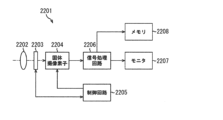
- FIG. 15 is a block diagram showing a configuration example of an imaging device as an electronic device to which the present technology is applied.
- An imaging device 2201 shown in FIG. 15 comprises an optical system 2202, a shutter device 2203, a solid-state imaging device 2204 as a photodetector, a control circuit 2205, a signal processing circuit 2206, a monitor 2207, and two memories 2208. Still images and moving images can be captured.
- the optical system 2202 has one or more lenses, guides the light (incident light) from the subject to the solid-state imaging device 2204, and forms an image on the light-receiving surface of the solid-state imaging device 2204.
- FIG. The shutter device 2203 is arranged between the optical system 2202 and the solid-state image sensor 2204 and controls the light irradiation period and the light shielding period for the solid-state image sensor 2204 according to the control of the control circuit 2205 .
- the solid-state imaging device 2204 is composed of a package including the above-described solid-state imaging device.
- the solid-state imaging device 2204 accumulates signal charges for a certain period of time according to the light imaged on the light receiving surface via the optical system 2202 and the shutter device 2203 .
- the signal charges accumulated in the solid-state imaging device 2204 are transferred according to the drive signal (timing signal) supplied from the control circuit 2205 .
- the control circuit 2205 drives the solid-state image sensor 2204 and the shutter device 2203 by outputting drive signals for controlling the transfer operation of the solid-state image sensor 2204 and the shutter operation of the shutter device 2203 .
- a signal processing circuit 2206 performs various signal processing on the signal charges output from the solid-state imaging device 2204 .
- An image (image data) obtained by the signal processing performed by the signal processing circuit 2206 is supplied to the monitor 2207 to be displayed, or supplied to the memory 2208 to be stored (recorded). Also in the imaging device 2201 configured in this way, the photodetectors 1A, 1B, 1C, 1D, 1E, and 1F can be applied in place of the solid-state imaging device 2204 described above.
- the technology (the present technology) according to the present disclosure can be applied to various products.
- the technology according to the present disclosure can be realized as a device mounted on any type of moving body such as automobiles, electric vehicles, hybrid electric vehicles, motorcycles, bicycles, personal mobility, airplanes, drones, ships, and robots. may
- FIG. 16 is a block diagram showing a schematic configuration example of a vehicle control system, which is an example of a mobile control system to which the technology according to the present disclosure can be applied.
- Vehicle control system 12000 comprises a plurality of electronic control units connected via communication network 12001 .
- the vehicle control system 12000 includes a drive train control unit 12010, a body system control unit 12020, an outside information detection unit 12030, an inside information detection unit 12040, and an integrated control unit 12050.
- a microcomputer 12051, an audio/image output unit 12052, and an in-vehicle network I/F (interface) 12053 are illustrated.
- the drive system control unit 12010 controls the operation of devices related to the drive system of the vehicle according to various programs.
- the driving system control unit 12010 includes a driving force generator for generating driving force of the vehicle such as an internal combustion engine or a driving motor, a driving force transmission mechanism for transmitting the driving force to the wheels, and a steering angle of the vehicle. It functions as a control device such as a steering mechanism to adjust and a brake device to generate braking force of the vehicle.
- the body system control unit 12020 controls the operation of various devices equipped on the vehicle body according to various programs.
- the body system control unit 12020 functions as a keyless entry system, a smart key system, a power window device, or a control device for various lamps such as headlamps, back lamps, brake lamps, winkers or fog lamps.
- body system control unit 12020 can receive radio waves transmitted from a portable device that substitutes for a key or signals from various switches.
- the body system control unit 12020 receives the input of these radio waves or signals and controls the door lock device, power window device, lamps, etc. of the vehicle.
- the vehicle exterior information detection unit 12030 detects information outside the vehicle in which the vehicle control system 12000 is installed.
- the vehicle exterior information detection unit 12030 is connected with an imaging section 12031 .
- the vehicle exterior information detection unit 12030 causes the imaging unit 12031 to capture an image of the exterior of the vehicle, and receives the captured image.
- the vehicle exterior information detection unit 12030 may perform object detection processing or distance detection processing such as people, vehicles, obstacles, signs, or characters on the road surface based on the received image.
- the imaging unit 12031 is an optical sensor that receives light and outputs an electrical signal according to the amount of received light.
- the imaging unit 12031 can output the electric signal as an image, and can also output it as distance measurement information.
- the light received by the imaging unit 12031 may be visible light or non-visible light such as infrared rays.
- the in-vehicle information detection unit 12040 detects in-vehicle information.
- the in-vehicle information detection unit 12040 is connected to, for example, a driver state detection section 12041 that detects the state of the driver.
- the driver state detection unit 12041 includes, for example, a camera that captures an image of the driver, and the in-vehicle information detection unit 12040 detects the degree of fatigue or concentration of the driver based on the detection information input from the driver state detection unit 12041. It may be calculated, or it may be determined whether the driver is dozing off.
- the microcomputer 12051 calculates control target values for the driving force generator, the steering mechanism, or the braking device based on the information inside and outside the vehicle acquired by the vehicle exterior information detection unit 12030 or the vehicle interior information detection unit 12040, and controls the drive system control unit.
- a control command can be output to 12010 .
- the microcomputer 12051 realizes the functions of ADAS (Advanced Driver Assistance System) including collision avoidance or shock mitigation, follow-up driving based on inter-vehicle distance, vehicle speed maintenance driving, vehicle collision warning, or vehicle lane deviation warning. Cooperative control can be performed for the purpose of ADAS (Advanced Driver Assistance System) including collision avoidance or shock mitigation, follow-up driving based on inter-vehicle distance, vehicle speed maintenance driving, vehicle collision warning, or vehicle lane deviation warning. Cooperative control can be performed for the purpose of ADAS (Advanced Driver Assistance System) including collision avoidance or shock mitigation, follow-up driving based on inter-vehicle distance, vehicle speed maintenance driving, vehicle collision warning, or vehicle
- the microcomputer 12051 controls the driving force generator, the steering mechanism, the braking device, etc. based on the information about the vehicle surroundings acquired by the vehicle exterior information detection unit 12030 or the vehicle interior information detection unit 12040, so that the driver's Cooperative control can be performed for the purpose of autonomous driving, etc., in which vehicles autonomously travel without depending on operation.
- the microcomputer 12051 can output a control command to the body system control unit 12020 based on the information outside the vehicle acquired by the information detection unit 12030 outside the vehicle.
- the microcomputer 12051 controls the headlamps according to the position of the preceding vehicle or the oncoming vehicle detected by the vehicle exterior information detection unit 12030, and performs cooperative control aimed at anti-glare such as switching from high beam to low beam. It can be carried out.
- the audio/image output unit 12052 transmits at least one of audio and/or image output signals to an output device capable of visually or audibly notifying the passengers of the vehicle or the outside of the vehicle.
- an audio speaker 12061, a display unit 12062, and an instrument panel 12063 are illustrated as output devices.
- the display unit 12062 may include at least one of an on-board display and a head-up display, for example.
- FIG. 17 is a diagram showing an example of the installation position of the imaging unit 12031.
- vehicle 12100 has imaging units 12101 , 12102 , 12103 , 12104 , and 12105 as imaging unit 12031 .
- the imaging units 12101, 12102, 12103, 12104, and 12105 are provided at positions such as the front nose of the vehicle 12100, the side mirrors, the rear bumper, the back door, and the upper part of the windshield in the vehicle interior, for example.
- An image pickup unit 12101 provided in the front nose and an image pickup unit 12105 provided above the windshield in the passenger compartment mainly acquire images in front of the vehicle 12100 .
- Imaging units 12102 and 12103 provided in the side mirrors mainly acquire side images of the vehicle 12100 .
- An imaging unit 12104 provided in the rear bumper or back door mainly acquires an image behind the vehicle 12100 .
- Forward images acquired by the imaging units 12101 and 12105 are mainly used for detecting preceding vehicles, pedestrians, obstacles, traffic lights, traffic signs, lanes, and the like.
- FIG. 17 shows an example of the imaging range of the imaging units 12101 to 12104.
- the imaging range 12111 indicates the imaging range of the imaging unit 12101 provided in the front nose
- the imaging ranges 12112 and 12113 indicate the imaging ranges of the imaging units 12102 and 12103 provided in the side mirrors, respectively
- the imaging range 12114 The imaging range of an imaging unit 12104 provided in the rear bumper or back door is shown. For example, by superimposing the image data captured by the imaging units 12101 to 12104, a bird's-eye view image of the vehicle 12100 viewed from above can be obtained.
- At least one of the imaging units 12101 to 12104 may have a function of acquiring distance information.
- at least one of the imaging units 12101 to 12104 may be a stereo camera composed of a plurality of imaging elements, or may be an imaging element having pixels for phase difference detection.
- the microcomputer 12051 determines the distance to each three-dimensional object within the imaging ranges 12111 to 12114 and changes in this distance over time (relative velocity with respect to the vehicle 12100). , it is possible to extract, as the preceding vehicle, the closest three-dimensional object on the course of the vehicle 12100, which runs at a predetermined speed (for example, 0 km/h or more) in substantially the same direction as the vehicle 12100. can. Furthermore, the microcomputer 12051 can set the inter-vehicle distance to be secured in advance in front of the preceding vehicle, and perform automatic brake control (including following stop control) and automatic acceleration control (including following start control). In this way, cooperative control can be performed for the purpose of automatic driving in which the vehicle runs autonomously without relying on the operation of the driver.
- automatic brake control including following stop control
- automatic acceleration control including following start control
- the microcomputer 12051 converts three-dimensional object data related to three-dimensional objects to other three-dimensional objects such as motorcycles, ordinary vehicles, large vehicles, pedestrians, and utility poles. It can be classified and extracted and used for automatic avoidance of obstacles. For example, the microcomputer 12051 distinguishes obstacles around the vehicle 12100 into those that are visible to the driver of the vehicle 12100 and those that are difficult to see. Then, the microcomputer 12051 judges the collision risk indicating the degree of danger of collision with each obstacle, and when the collision risk is equal to or higher than the set value and there is a possibility of collision, an audio speaker 12061 and a display unit 12062 are displayed. By outputting an alarm to the driver via the drive system control unit 12010 and performing forced deceleration and avoidance steering via the drive system control unit 12010, driving support for collision avoidance can be performed.
- At least one of the imaging units 12101 to 12104 may be an infrared camera that detects infrared rays.
- the microcomputer 12051 can recognize a pedestrian by determining whether or not the pedestrian exists in the captured images of the imaging units 12101 to 12104 .
- recognition of a pedestrian is performed by, for example, a procedure for extracting feature points in images captured by the imaging units 12101 to 12104 as infrared cameras, and performing pattern matching processing on a series of feature points indicating the outline of an object to determine whether or not the pedestrian is a pedestrian.
- the audio image output unit 12052 outputs a rectangular outline for emphasis to the recognized pedestrian. is superimposed on the display unit 12062 . Also, the audio/image output unit 12052 may control the display unit 12062 to display an icon or the like indicating a pedestrian at a desired position.
- the technology according to the present disclosure can be applied to, for example, the imaging unit 12031 among the configurations described above.
- the photodetector 1A in FIG. 1, the photodetector 1B in FIG. 10, the photodetector 1C in FIG. 11, the photodetector 1D in FIG. 12, the photodetector 1E in FIG. 13, and the photodetector in FIG. 14A Apparatus 1F can be applied.
- the pixel area is a light transmission layer made of a first compound semiconductor and transmitting incident infrared light;
- a photoelectric device that is laminated on the surface of the light transmission layer opposite to the light incident surface, is made of a second compound semiconductor different from the first compound semiconductor, and photoelectrically converts infrared light that has passed through the light transmission layer.
- the light transmission layer is a first semiconductor layer provided on the light incident surface side and having a thickness capable of transmitting the visible light;
- the photodetector according to (1) further comprising a passivation layer disposed on the light incident surface side of the light transmission layer and transmitting the infrared light and the visible light.
- the photodetector according to (1) above which is disposed on the light incident surface side of the light transmission layer and has a transparent electrode and a passivation layer that transmit the infrared light and the visible light.
- the second semiconductor layer is configured by stacking a plurality of layers, The impurity concentration of the first stage positioned closer to the photoelectric conversion layer among the plurality of stages is lower than the impurity concentration of the second stage stacked closer to the light incident surface than the first stage. photodetector.
- the first semiconductor layer has a thickness of 5 ⁇ 10 17 cm ⁇ 3 or more and 30 nm or less.
- the pixel area is a light transmission layer made of a first compound semiconductor and transmitting incident infrared light;
- a photoelectric device that is laminated on the surface of the light transmission layer opposite to the light incident surface, is made of a second compound semiconductor different from the first compound semiconductor, and photoelectrically converts infrared light that has passed through the light transmission layer.
- the light transmission layer is a first semiconductor layer provided on the light incident surface side and having a thickness capable of transmitting the visible light;
- a second semiconductor layer laminated on the surface opposite to the light incident surface of the first semiconductor layer and photoelectrically converting visible light transmitted through the first semiconductor layer,
- the second semiconductor layer has a lower impurity concentration than the first semiconductor layer and a photodetector device having a higher impurity concentration than the photoelectric conversion layer, Electronics.
- Photodetector 2 Semiconductor chip 2A Pixel region 2B Peripheral regions 3, 3a, 3b Pixel 4 Vertical drive circuit 5 Column signal processing circuit 6 Horizontal drive circuit 7 Output circuit 8 Control circuit 10 Pixel Drive wiring 11 Vertical signal wiring 12 Horizontal signal wiring 13 Logic circuit 14 Bonding pad (input/output terminal) 15 readout circuit 20 photoelectric conversion substrate 22, 73, 93 recombination prevention layers 23, 72, 81, 82 second compound semiconductor layers 23x, 25x first surfaces 23y, 25y second surface 25 first compound semiconductor layer 26 , 71 photoelectric conversion layer 27 cap layer 28 contact region 29 protective film 29a openings 31, 41 connection electrode 40 circuit board portion 42 bump electrode 43 insulating layer 51 first light transmitting portion 52 second light transmitting portion 57 microlens ( on-chip lens) 61 Infrared light 62 Visible light 91 Transparent electrode 92 Passivation layer 811 First step layer 812 Second step layer 2201 Imaging device 2202 Optical system 2
Landscapes
- Physics & Mathematics (AREA)
- Engineering & Computer Science (AREA)
- Power Engineering (AREA)
- Electromagnetism (AREA)
- Condensed Matter Physics & Semiconductors (AREA)
- General Physics & Mathematics (AREA)
- Computer Hardware Design (AREA)
- Microelectronics & Electronic Packaging (AREA)
- Light Receiving Elements (AREA)
Abstract
可視光感度を維持しつつ、結晶欠陥をでき難くし得る光検出装置及び電子機器を提供する。光検出装置は、外部から入射した赤外光及び可視光に応じて電気信号を生成可能な複数の画素が行列状に配置された画素領域を備える。画素領域は、光透過層と、光電変換層とを備える。光透過層は、第1の化合物半導体から成り、入射した赤外光を透過する。光電変換層は、光透過層の光入射面とは反対側の面に積層され、第1の化合物半導体とは異なる第2の化合物半導体から成り、光透過層を透過した赤外光を光電変換する。光透過層は、光入射面側に設けられ、可視光を透過可能な厚みを有する第1の半導体層と、第1の半導体層の光入射面とは反対側の面に積層され、第1の半導体層を透過した可視光を光電変換する第2の半導体層とを備える。第2の半導体層は、第1の半導体層より不純物濃度が薄く、光電変換層より不純物濃度が濃い。
Description
本開示は、光検出装置、及びこの光検出装置を備えた電子機器に関する。
周知のように、赤色の光(R)、緑色の光(G)、青色の光(B)といった可視光を検出するイメージセンサに備えられる撮像素子は、通常、シリコン半導体基板に形成された受光素子(フォトダイオード)を備えている。ところで、赤外光を検出することも、従来から要望されている。しかし、シリコンのエネルギーバンドギャップは1.1eVであるため、1.1μmよりも長波長の赤外光(IR)を検出することは原理的にできない。
このため、シリコンの代わりに、InGaAsを用いることで、赤外光を検出することが可能なInGaAsイメージセンサがある。このInGaAsイメージセンサでは、InP基板上にInGaAsを成膜して作成し、InP基板側から光を入射することが知られている。しかし、InGaAsイメージセンサでは、光入射側のInP基板を取り除かないと可視光を検出することができない。
そこで、InGaAsイメージセンサで光入射側のn+InP層(暗電流発生を抑制する再結合防止層)を薄くすることで、可視光感度をアップできる手法が知られている(例えば、特許文献1)。
ところで、n+InP層が薄いとプロセス中のダメージがバンドギャップの狭いInGaAs層まで届き結晶欠陥ができて白傷になる。また、光入射側のInP層の不純物濃度を低くすることで、InP層で光電変換可能になり厚膜化しても可視光感度は落ちにくいが、界面欠陥で湧き出たキャリアも読み出してしまうため、白傷になる。
本開示はこのような事情に鑑みてなされたもので、可視光感度を維持しつつ、結晶欠陥をでき難くし得る光検出装置及び電子機器を提供することを目的とする。
本開示の一態様は、外部から入射した赤外光及び可視光に応じて電気信号を生成可能な複数の画素が行列状に配置された画素領域を備え、前記画素領域は、第1の化合物半導体から成り、入射した赤外光を透過する光透過層と、前記光透過層の光入射面とは反対側の面に積層され、前記第1の化合物半導体とは異なる第2の化合物半導体から成り、前記光透過層を透過した赤外光を光電変換する光電変換層とを備え、前記光透過層は、光入射面側に設けられ、前記可視光を透過可能な厚みを有する第1の半導体層と、前記第1の半導体層の光入射面とは反対側の面に積層され、前記第1の半導体層を透過した可視光を光電変換する第2の半導体層とを備え、前記第2の半導体層は、前記第1の半導体層より不純物濃度が薄く、前記光電変換層より不純物濃度が濃い光検出装置である。
本開示の他の態様は、外部から入射した赤外光及び可視光に応じて電気信号を生成可能な複数の画素が行列状に配置された画素領域を備え、前記画素領域は、第1の化合物半導体から成り、入射した赤外光を透過する光透過層と、前記光透過層の光入射面とは反対側の面に積層され、前記第1の化合物半導体とは異なる第2の化合物半導体から成り、前記光透過層を透過した赤外光を光電変換する光電変換層とを備え、前記光透過層は、光入射面側に設けられ、前記可視光を透過可能な厚みを有する第1の半導体層と、前記第1の半導体層の光入射面とは反対側の面に積層され、前記第1の半導体層を透過した可視光を光電変換する第2の半導体層とを備え、前記第2の半導体層は、前記第1の半導体層より不純物濃度が薄く、前記光電変換層より不純物濃度が濃い光検出装置を備えた、電子機器である。
以下において、図面を参照して本開示の実施形態を説明する。以下の説明で参照する図面の記載において、同一又は類似の部分には同一又は類似の符号を付し、重複する説明を省略する。但し、図面は模式的なものであり、厚みと平面寸法との関係、各装置や各部材の厚みの比率等は現実のものと異なることに留意すべきである。したがって、具体的な厚みや寸法は以下の説明を参酌して判定すべきものである。また、図面相互間においても互いの寸法の関係や比率が異なる部分が含まれていることは勿論である。
本明細書において、「第1導電型」はp型又はn型の一方であり、「第2導電型」はp型又はn型のうちの「第1導電型」とは異なる一方を意味する。また、「n」や「p」に付す「+」や「-」は、「+」及び「-」が付記されていない半導体領域に比して、それぞれ相対的に不純物密度が高い又は低い半導体領域であることを意味する。但し、同じ「n」と「n」とが付された半導体領域であっても、それぞれの半導体領域の不純物密度が厳密に同じであることを意味するものではない。
また、以下の説明における上下等の方向の定義は、単に説明の便宜上の定義であって、本開示の技術的思想を限定するものではない。例えば、対象を90°回転して観察すれば上下は左右に変換して読まれ、180°回転して観察すれば上下は反転して読まれることは勿論である。
なお、本明細書中に記載される効果はあくまで例示であって限定されるものでは無く、また他の効果があってもよい。
なお、本明細書中に記載される効果はあくまで例示であって限定されるものでは無く、また他の効果があってもよい。
<第1の実施形態>
(光検出装置の全体構成)
まず、光検出装置1Aの全体構成について説明する。
図1は、本開示の第1の実施形態に係る光検出装置の一構成例を示す模式的平面レイアウト図である。
本開示の第1の実施形態に係る光検出装置1Aは、平面視したときの二次元平面形状が方形状の半導体チップ2を主体に構成されている。すなわち、光検出装置1Aは、半導体チップ2に搭載されている。この光検出装置1Aは、光学レンズ(図示せず)を介して被写体からの入射光を取り込み、撮像面上に結像された入射光の光量を画素単位で電気信号に変換して画素信号として出力する。
(光検出装置の全体構成)
まず、光検出装置1Aの全体構成について説明する。
図1は、本開示の第1の実施形態に係る光検出装置の一構成例を示す模式的平面レイアウト図である。
本開示の第1の実施形態に係る光検出装置1Aは、平面視したときの二次元平面形状が方形状の半導体チップ2を主体に構成されている。すなわち、光検出装置1Aは、半導体チップ2に搭載されている。この光検出装置1Aは、光学レンズ(図示せず)を介して被写体からの入射光を取り込み、撮像面上に結像された入射光の光量を画素単位で電気信号に変換して画素信号として出力する。
光検出装置1Aが搭載された半導体チップ2は、二次元平面において、中央部に設けられた方形状の画素領域2Aと、この画素領域2Aの外側に画素領域2Aを囲むようにして配置された周辺領域2Bとを備えている。
画素領域2Aは、例えば光学レンズにより集光される光を受光する受光面である。そして、画素領域2Aには、X方向及びY方向を含む二次元平面において複数の画素3が行列状に配置されている。換言すれば、画素3は、二次元平面内で互いに直交するX方向及びY方向のそれぞれの方向に繰り返し配置されている。
周辺領域2Bには、複数のボンディングパッド(入出力端子)14が配置されている。複数のボンディングパッド14の各々は、例えば、半導体チップ2の二次元平面における4つの辺に沿って配列されている。複数のボンディングパッド14の各々は、半導体チップ2を外部装置と電気的に接続する際に用いられる入出力端子である。
(ロジック回路)
図2は、上記光検出装置1Aの一構成例を示すブロック図である。
半導体チップ2は、垂直駆動回路4、カラム信号処理回路5、水平駆動回路6、出力回路7及び制御回路8などを含むロジック回路13を備えている。ロジック回路13は、例えば、nチャネル導電型のMOSFET(Metal Oxide Semiconductor Field Effect Transistor)及びpチャネル導電型のMOSFETを有するCMOS(Complenentary MOS)回路で構成されている。
図2は、上記光検出装置1Aの一構成例を示すブロック図である。
半導体チップ2は、垂直駆動回路4、カラム信号処理回路5、水平駆動回路6、出力回路7及び制御回路8などを含むロジック回路13を備えている。ロジック回路13は、例えば、nチャネル導電型のMOSFET(Metal Oxide Semiconductor Field Effect Transistor)及びpチャネル導電型のMOSFETを有するCMOS(Complenentary MOS)回路で構成されている。
垂直駆動回路4は、例えばシフトレジスタによって構成されている。垂直駆動回路4は、所望の画素駆動配線10を順次選択し、選択した画素駆動配線10に画素3を駆動するためのパルスを供給し、各画素3を行単位で駆動する。即ち、垂直駆動回路4は、画素領域2Aの各画素3を行単位で順次垂直方向に選択走査し、各画素3の光電変換素子が受光量に応じて生成した信号電荷に基づく画素3からの画素信号を、垂直信号配線11を通してカラム信号処理回路5に供給する。
カラム信号処理回路5は、例えば画素3の列毎に配置されており、1行分の画素3から出力される信号に対して画素列毎にノイズ除去等の信号処理を行う。例えばカラム信号処理回路5は、画素固有の固定パターンノイズを除去するためのCDS(Correlated Double Sampling:相関2重サンプリング)及びAD(Analog Digital)変換等の信号処理を行う。
水平駆動回路6は、例えばシフトレジスタによって構成されている。水平駆動回路6は、水平走査パルスをカラム信号処理回路5に順次出力することによって、カラム信号処理回路5の各々を順番に選択し、カラム信号処理回路5の各々から信号処理が行われた画素信号を水平信号配線12に出力させる。
出力回路7は、カラム信号処理回路5の各々から水平信号配線12を通して順次に供給される画素信号に対し、信号処理を行って出力する。信号処理としては、例えば、バッファリング、黒レベル調整、列ばらつき補正、各種デジタル信号処理等を用いることができる。
制御回路8は、垂直同期信号、水平同期信号、及びマスタクロック信号に基づいて、垂直駆動回路4、カラム信号処理回路5、及び水平駆動回路6等の動作の基準となるクロック信号や制御信号を生成する。そして、制御回路8は、生成したクロック信号や制御信号を、垂直駆動回路4、カラム信号処理回路5、及び水平駆動回路6等に出力する。
(光電変換素子及び読出し回路)
図3は、上記光検出装置1Aの読出し回路15の一構成例を示す回路図である。
複数の画素の各々の画素3は、光電変換素子PDを有している。そして、各画素3の光電変換素子PDには、読出し回路15が接続されている。光電変換素子PDは、受光した光量に応じた電荷(信号電荷)を生成する。光電変換素子PDのカソード側には、所定のバイアス電圧Vaが印加される。
図3は、上記光検出装置1Aの読出し回路15の一構成例を示す回路図である。
複数の画素の各々の画素3は、光電変換素子PDを有している。そして、各画素3の光電変換素子PDには、読出し回路15が接続されている。光電変換素子PDは、受光した光量に応じた電荷(信号電荷)を生成する。光電変換素子PDのカソード側には、所定のバイアス電圧Vaが印加される。
読出し回路15は、光電変換素子PDのアノード側に接続されている。読出し回路15は、電荷蓄積部(電荷保持部)としての容量素子Cpと、リセットトランジスタRSTと、増幅トランジスタAMPと、選択トランジスタSELと、を有している。これらのトランジスタ(RST,AMP,SEL)は、例えば、酸化シリコン膜をゲート絶縁膜とするMOSFETで構成されている。また、これらのトランジスタ(RST,AMP,SEL)は、窒化シリコン(Si3N4)膜、或いは窒化シリコン膜及び酸化シリコン膜などの積層膜をゲート絶縁膜とするMISFET(Metal Insulator Semiconductor FET)でも構わない。
容量素子Cpは、光電変換素子PDで生成された信号電荷を蓄積する。容量素子Cpは、例えば、pn接合容量、MOS容量、及び配線容量の何れかによって構成されている。
リセットトランジスタRSTは、ゲート電極にリセット信号が印加されてオン状態となると、容量素子Cpに蓄積されている信号電荷を排出し、容量素子Cpの電位をリセットする。
リセットトランジスタRSTは、ゲート電極にリセット信号が印加されてオン状態となると、容量素子Cpに蓄積されている信号電荷を排出し、容量素子Cpの電位をリセットする。
増幅トランジスタAMPは、容量素子Cpの蓄積電位に応じた画素信号を出力する。具体的には、増幅トランジスタAMPは、垂直信号配線11を介して接続されている定電流源としての負荷MOSとソースフォロワ回路とを構成している。ソースフォロワ回路は、容量素子Cpに蓄積されている信号電荷に応じたレベルを示す画素信号を増幅トランジスタAMPから選択トランジスタSEL及び垂直信号配線11を介してカラム信号処理回路5に出力する。
選択トランジスタSELは、ゲート電極に選択信号が印加されてオン状態となると、垂直信号配線11を介してカラム信号処理回路5に画素3の画素信号を出力する。選択信号が転送される信号配線及びリセット信号が転送される信号線は、図2の画素駆動配線10に対応する。
(光検出装置の具体的な構成)
次に、光検出装置1Aの具体的な構成について説明する。
図4は、光検出装置1Aの一構成例を示す要部模式的断面図である。
半導体チップ2は、互いに向かい合って積層された光電変換基板部20及び回路基板部40を備えている。光電変換基板部20には、上述の画素領域2Aなどが構成されている。回路基板部40には、上述のロジック回路13、ボンディングパッド14、及び読出し回路15などが構成されている。
次に、光検出装置1Aの具体的な構成について説明する。
図4は、光検出装置1Aの一構成例を示す要部模式的断面図である。
半導体チップ2は、互いに向かい合って積層された光電変換基板部20及び回路基板部40を備えている。光電変換基板部20には、上述の画素領域2Aなどが構成されている。回路基板部40には、上述のロジック回路13、ボンディングパッド14、及び読出し回路15などが構成されている。
(光電変換基板部20)
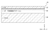
光電変換基板部20は、互いに反対側に位置する第1の面25x及び第2の面25yを有する第1化合物半導体層25と、この第1化合物半導体層25の第2の面25y側に配置された第2化合物半導体層23とを備えている。この第2化合物半導体層23の第2の面23y側に配置された第2化合物半導体層としての再結合防止層22とを備えている。これら第1化合物半導体層25、第2化合物半導体層23及び再結合防止層22の各々は、各画素3に共通して設けられている。そして、第1化合物半導体層25には、上述の光電変換素子PDが画素3毎に設けられている。再結合防止層22は、暗電流発生を抑制する。
ここで、第1化合物半導体層25の第1の面25xを素子形成面又は主面、第2の面25yを光入射面又は裏面と呼ぶこともある。また、第2化合物半導体層23の互いに反対側に位置する第1の面23x及び第2の面23yにおいても、第1の面23xを主面、第2の面23yを光入射面又は裏面と呼ぶこともある。
また、図4に示すように、光電変換基板部20は、第1化合物半導体層25の第1の面25x側に、第1の面25xを覆う保護膜29を更に備えている。保護膜29は、各画素3に共通して設けられている。また、光電変換基板部20は、再結合防止層22の光入射面側に、遮光膜(図示せず)と、反射防止膜(図示せず)と、平坦化膜(図示せず)と、マイクロレンズ(オンチップレンズ)57と、を更に備えている。再結合防止層22及び第2化合物半導体層23は、赤外領域の波長の光(赤外光61)及び可視領域の波長の光(可視光62)を透過する光透過層を構成する。
第1化合物半導体層25は、例えば、第1の面25x側から光電変換層26及びキャップ層27を含んでいる。そして、再結合防止層22、第2化合物半導体層23、第1化合物半導体層25の光電変換層26及びキャップ層27は、この順で成長基板(図示せず)にエピタキシャル成長させて形成されたエピタキシャル層である。すなわち、第1化合物半導体層25は、光電変換層26とキャップ層27とが共有結合され、更に光電変換層26が第2化合物半導体層23と共有結合されている。
キャップ層27は、例えば、全ての画素3に共通して設けられ、保護膜29と光電変換層26との間に配置されている。キャップ層27には例えば半導体領域(不純物拡散領域)からなる複数のコンタクト領域28が設けられている。キャップ層27に、光電変換層26を構成する化合物半導体材料のバンドギャップ(Eg)よりも大きなバンドギャップ(Eg)の化合物半導体材料を用いることにより、暗電流を抑えることも可能となる。キャップ層27としては、例えばn型のInP(インジウムリン)を用いることができる。
複数のコンタクト領域28の各々のコンタクト領域28は、互いに離間して画素3毎に配置されている。そして、各々のコンタクト領域28には、保護膜29に設けられた開口部29aを通して接続電極(素子側接続電極)31がそれぞれ個別に接続されている。
コンタクト領域28は、光電変換層26で発生した信号電荷を画素3毎に読み出すためのものであり、例えばp型を呈する不純物を含んでいる。p型を呈する不純物としては、例えばZn(亜鉛)などが挙げられる。このように、コンタクト領域28と、コンタクト領域28以外のキャップ層27との間にpn接合界面が形成され、隣り合う画素3が電気的に分離されるようになっている。コンタクト領域28は、キャップ層27の厚さよりも厚く構成され、光電変換層26の厚さ方向(Z方向)の一部にも設けられている。
キャップ層27と第2化合物半導体層23との間の光電変換層26は、例えば、全ての画素3に共通して設けられている。この光電変換層26は、所定の波長の光、この第1の実施形態では赤外光61及び可視光62を吸収して信号電荷を発生させるものであり、例えば、n型を呈する不純物を含むIII-V族化合物半導体材料、若しくはi型のIII-V族化合物半導体材料により構成されている。光電変換層26を構成する化合物半導体材料としては、例えば、InGaAs(インジウムガリウム砒素)、及びInGaAs/GaAsSb(インジウムガリウムアンチモン)の何れかを含む化合物半導体を採用することができる。この第1の実施形態では、光電変換層26としてi型のInGaAsを用いている。光電変換層26では、赤外領域の波長の光及び可視領域の波長の光を光電変換するようになっている。
この第1実施形態では、再結合防止層22及び第2化合物半導体層23が全ての画素3に共通して設けられている。再結合防止層22及び第2化合物半導体層23は、各画素3に共通の電極としても機能し、光電変換層26で発生した電荷のうち、信号電荷として用いられない電荷を排出する(カソード)。例えば、正孔が、信号電荷として接続電極31から読み出される場合には、再結合防止層22及び第2化合物半導体層23を通じて例えば電子を排出することができる。再結合防止層22及び第2化合物半導体層23には、所定のバイアス電圧Vaが印加される。
接続電極(素子側接続電極)31は、光電変換層26で発生した信号電荷(正孔又は電子、以下便宜上、信号電荷が正孔であるとして説明する。)を読み出すための電圧が供給される電極(アノード)であり、画素領域2Aにおいて画素3毎に設けられている。すなわち、接続電極31、光電変換層26、及び、電極としても機能する再結合防止層22及び第2化合物半導体層23を含む光電変換素子PDが画素3毎に設けられている。そして、接続電極31は光電変換素子PDのアノード側電極として機能し、再結合防止層22及び第2化合物半導体層23は光電変換素子PDのカソード側電極として機能する。
接続電極31は、例えば、チタン(Ti)、タングステン(W)、窒化チタン(TiN)、白金(Pt)、金(Au)、ゲルマニウム(Ge)、パラジウム(Pd)、亜鉛(Zn)、ニッケル(Ni)及びアルミニウム(Al)のうちの何れかの単体、又はそれらのうちの少なくとも1種を含む合金により構成されている。接続電極31は、このような構成材料の単膜であってもよく、或いは、2種以上を組み合わせた積層膜であってもよい。例えば、接続電極31は、チタン及びタングステンの積層膜により構成され、数十nmから数百nm程度の膜厚で構成されている。
図4に示すように、保護膜29は、第1化合物半導体層25と絶縁層43との間に設けられている。保護膜29は、例えば、酸化シリコン(SiOx)又は酸化アルミニウム(Al2O3)などの酸化物を含んで構成されている。保護膜29は、複数の膜を積層した積層構造で構成してもよい。保護膜29は、例えば酸窒化シリコン(SiON),炭素含有酸化シリコン(SiOC),窒化シリコン(SiN)及びシリコンカーバイド(SiC)などのシリコン(Si)系絶縁材料により構成するようにしてもよい。保護膜29の厚さは、例えば数十nmから数百nm程度である。
図4に示すように、再結合防止層22及び第2化合物半導体層23は、第1化合物半導体層25の光電変換層26よりも不純物濃度が高いn型の化合物半導体で構成され、上述したように電極としての機能も兼ね備えている。
再結合防止層22及び第2化合物半導体層23の材料としては、InP、InGaAsP、InGaAlAs、InAlAs、InAlAsSb、及びAlAsSbの何れかを含む化合物半導体を採用することができる。この第1の実施形態では、再結合防止層22及び第2化合物半導体層23を構成する化合物半導体材料として、n型を呈する不純物を含むInPを用いている。この第2化合物半導体層23と上述の第1化合物半導体層25とでは、化合物半導体材料が異なっている。
(InPの膜厚及び光透過率)
図5は、InPの膜厚と光透過率との依存性を示す特性図である。図5では、InPの膜厚が20nm、50nm、100nm、200nm、500nm、及び1000nmの場合を示している。赤外光の波長範囲は、およそ780nmから1mmである。可視光の波長範囲は、およそ下限360-400nmから上限760-830nmである。
図5は、InPの膜厚と光透過率との依存性を示す特性図である。図5では、InPの膜厚が20nm、50nm、100nm、200nm、500nm、及び1000nmの場合を示している。赤外光の波長範囲は、およそ780nmから1mmである。可視光の波長範囲は、およそ下限360-400nmから上限760-830nmである。
図5に示すように、光の波長帯が概ね950nm以下では光透過率が膜厚に依存し、膜厚が薄くなるに従って光透過率が大きくなり、膜厚が厚くなるに従って透過率が小さくなる。
図4に示すように、マイクロレンズ57は、再結合防止層22の光入射面側に設けられている。マイクロレンズ57は、画素領域2Aにおいて、画素3毎に設けられ、複数の画素3の配置に対応して行列状に配置されている。マイクロレンズ57は、照射光を集光し、集光した光を、画素3に効率よく入射させる。マイクロレンズ57は、例えば樹脂系材料で構成されている。
(回路基板部40)
図4では具体的な構成について図示を省略しているが、回路基板部40は、例えば単結晶シリコンからなる半導体基板と、この半導体基板の厚さ方向(Z方向)において互いに反対側に位置する第1の面及び第2の面のうちの第1の面側に配置された多層配線層と、を備えている。この回路基板部40の半導体基板には、上述のロジック回路13や読出し回路15などの回路に含まれる能動素子や受動素子が設けられている。図4では、符号を省略して図3に示す読出し回路15を図示している。
図4では具体的な構成について図示を省略しているが、回路基板部40は、例えば単結晶シリコンからなる半導体基板と、この半導体基板の厚さ方向(Z方向)において互いに反対側に位置する第1の面及び第2の面のうちの第1の面側に配置された多層配線層と、を備えている。この回路基板部40の半導体基板には、上述のロジック回路13や読出し回路15などの回路に含まれる能動素子や受動素子が設けられている。図4では、符号を省略して図3に示す読出し回路15を図示している。
図4に示すように、回路基板部40の最上層の配線層には、接続電極41が設けられている。接続電極41は、光電変換基板部20の接続電極31に対応して配置されている。そして、接続電極41は、読出し回路15と電気的に接続されている。
回路基板部40の接続電極41は、バンプ電極42を介して光電変換基板部20の接続電極31と電気的及び機械的に接続されている。そして、回路基板部40と光電変換基板部20との間には、バンプ電極42を除いて絶縁層43が設けられている。回路基板部40及び光電変換基板部20は、バンプ電極42及び絶縁層43によって接合されている。回路基板部40の光電変換素子PDは、アノード側が、接続電極31、バンプ電極42及び接続電極41を介して読出し回路15と電気定的に接続されている。
<実施形態の比較例>
ところで、InGaAsイメージセンサでは、再結合防止層22の膜厚を薄くすることで、可視光感度をアップすることができるが、プロセス中のダメージが再結合防止層22よりバンドギャップの狭い光電変換層26まで届いてしまう。
ところで、InGaAsイメージセンサでは、再結合防止層22の膜厚を薄くすることで、可視光感度をアップすることができるが、プロセス中のダメージが再結合防止層22よりバンドギャップの狭い光電変換層26まで届いてしまう。
図6は、比較例におけるプロセスダメージの発生の一例を示す光検出装置1-1の断面図である。図6において、上記図4と同一部分には同一符号を付して詳細な説明を省略する。
図6において、光検出装置1-1では、再結合防止層22の膜厚が薄いとプロセス中のダメージが光電変換層26まで届き結晶欠陥ができて白傷になる。この白傷は、画像が作成されたときに画像中に白くなる部分が残る。
図6において、光検出装置1-1では、再結合防止層22の膜厚が薄いとプロセス中のダメージが光電変換層26まで届き結晶欠陥ができて白傷になる。この白傷は、画像が作成されたときに画像中に白くなる部分が残る。
一方、再結合防止層22の不純物濃度を低くする方法も考えられる。
図7は、比較例におけるプロセスダメージの発生の他の一例を示す光検出装置1-2の断面図である。図7において、上記図4と同一部分には同一符号を付して詳細な説明を省略する。
図7は、比較例におけるプロセスダメージの発生の他の一例を示す光検出装置1-2の断面図である。図7において、上記図4と同一部分には同一符号を付して詳細な説明を省略する。
図7において、光検出装置1-2では、再結合防止層22の不純物濃度を低くすることで、再結合防止層22で光電変換可能になり、再結合防止層22を厚膜化しても可視光感度は落ちにくいが、界面欠陥で湧き出たキャリアも読み出してしまうため、白傷になる。
<第1の実施形態の解決手段>
上述の課題に対し、本開示の第1の実施形態では、図8及び図9に示すように、再結合防止層22と光電変換層26との間に、再結合防止層22の不純物濃度より薄い不純物濃度を有する第2化合物半導体層23を設けるようにしている。
上述の課題に対し、本開示の第1の実施形態では、図8及び図9に示すように、再結合防止層22と光電変換層26との間に、再結合防止層22の不純物濃度より薄い不純物濃度を有する第2化合物半導体層23を設けるようにしている。
図8に示す再結合防止層22と第2化合物半導体層23とのトータルの膜厚は、以前のInGaAsイメージセンサの再結合防止層22の膜厚と同じである。このようにすれば、第2化合物半導体層23で可視光62が光電変換するため、可視光感度がアップする。また、トータルのInP層を厚くしても再結合防止層22を薄くすれば、可視光感度を維持しつつ、図9に示すように、プロセスダメージが光電変換層26に到達し難くなり、白傷の元となるInGaAs中の結晶欠陥ができ難くなる。
なお、再結合防止層22の膜厚は、5×1017cm-3以上、30nm以下の厚みである。また、第2化合物半導体層23の膜厚は、1×1017cm-3以上、1×1018cm-3以下である。光電変換層26の膜厚は、1×1017cm-3以下である。
さらに、第2化合物半導体層23の不純物濃度は、再結合防止層22より薄く、光電変換層26より濃い。再結合防止層22及び第2化合物半導体層23の不純物には、n型の場合に、Si(シリコン)、S(硫黄)のいずれかが用いられる。
さらに、第2化合物半導体層23の不純物濃度は、再結合防止層22より薄く、光電変換層26より濃い。再結合防止層22及び第2化合物半導体層23の不純物には、n型の場合に、Si(シリコン)、S(硫黄)のいずれかが用いられる。
<第1の実施形態による作用効果>
以上のように第1の実施形態によれば、光入射側の再結合防止層22と光電変換層26との間に、再結合防止層22より不純物濃度が薄く、光電変換層26より不純物濃度が濃い第2化合物半導体層23を設けることで、第2化合物半導体層23で光電変換された可視光62のキャリアを光電変換層26へ転送でき、これにより、可視光感度を維持しつつ、白傷の元になる光電変換層26に与えるプロセスダメージを低減できる。
以上のように第1の実施形態によれば、光入射側の再結合防止層22と光電変換層26との間に、再結合防止層22より不純物濃度が薄く、光電変換層26より不純物濃度が濃い第2化合物半導体層23を設けることで、第2化合物半導体層23で光電変換された可視光62のキャリアを光電変換層26へ転送でき、これにより、可視光感度を維持しつつ、白傷の元になる光電変換層26に与えるプロセスダメージを低減できる。
<第2の実施形態>
本開示の第2の実施形態は、光電変換層、再結合防止層、第2化合物半導体層がp型である例について説明する。
図10は、本開示の第2の実施形態に係る光検出装置1Bの断面図である。光検出装置1Bは、厚さ方向(図10中矢印Zで示す方向)に沿って、光電変換層71、第2化合物半導体層72、再結合防止層73という順に積層されている。
本開示の第2の実施形態は、光電変換層、再結合防止層、第2化合物半導体層がp型である例について説明する。
図10は、本開示の第2の実施形態に係る光検出装置1Bの断面図である。光検出装置1Bは、厚さ方向(図10中矢印Zで示す方向)に沿って、光電変換層71、第2化合物半導体層72、再結合防止層73という順に積層されている。
再結合防止層73の膜厚は、5×1017cm-3以上、30nm以下の厚みである。また、第2化合物半導体層72の膜厚は、1×1017cm-3以上、1×1018cm-3以下である。光電変換層71の膜厚は、1×1017cm-3以下である。
さらに、第2化合物半導体層72の不純物濃度は、再結合防止層73より薄く、光電変換層71より濃い。再結合防止層73及び第2化合物半導体層72の不純物には、Mg(マグネシウム)、Cd(カドミウム)、Al(アルミニウム)、Zn(亜鉛)のいずれかが用いられる。
さらに、第2化合物半導体層72の不純物濃度は、再結合防止層73より薄く、光電変換層71より濃い。再結合防止層73及び第2化合物半導体層72の不純物には、Mg(マグネシウム)、Cd(カドミウム)、Al(アルミニウム)、Zn(亜鉛)のいずれかが用いられる。
<第2の実施形態による作用効果>
以上のように第2の実施形態によれば、上記第1の実施形態と同様の作用効果が得られる。
以上のように第2の実施形態によれば、上記第1の実施形態と同様の作用効果が得られる。
<第3の実施形態>
本開示の第3の実施形態は、第2化合物半導体層を複数段の層を積層して構成する例について説明する。
図11は、本開示の第3の実施形態に係る光検出装置1Cの断面図である。図11において、上記図8と同一部分には同一符号を付して詳細な説明を省略する。
本開示の第3の実施形態は、第2化合物半導体層を複数段の層を積層して構成する例について説明する。
図11は、本開示の第3の実施形態に係る光検出装置1Cの断面図である。図11において、上記図8と同一部分には同一符号を付して詳細な説明を省略する。
第2化合物半導体層81は、1段層(n InP_1)811と、1段層811の光電変換層26側に積層された2段層(n InP_2)812とにより構成されている。第2化合物半導体層81の不純物濃度は、再結合防止層22より薄く、光電変換層26より濃く、1段層811の不純物濃度が2段層812の不純物濃度より濃い。
<第3の実施形態による作用効果>
以上のように第3の実施形態によれば、第2化合物半導体層81を、1段層811と、2段層812とにより構成し、光電変換層26側に位置する2段層812の不純物濃度を1段層811の不純物濃度より薄くすることで、光検出装置1Cの製造コストを安くして、可視光62の光電変換されたキャリアを光電変換層26へ転送することができる。
以上のように第3の実施形態によれば、第2化合物半導体層81を、1段層811と、2段層812とにより構成し、光電変換層26側に位置する2段層812の不純物濃度を1段層811の不純物濃度より薄くすることで、光検出装置1Cの製造コストを安くして、可視光62の光電変換されたキャリアを光電変換層26へ転送することができる。
なお、第3の実施形態では、第2化合物半導体層81を、2段以上の複数段の層で構成することもできる。このようにすれば、不純物濃度を光電変換層26へ向かうにつれて段ごとに薄くしていくことで、さらに可視光62の光電変換されたキャリアを光電変換層26へ転送することができる。
<第4の実施形態>
本開示の第4の実施形態は、第2化合物半導体層をグラデーションにより構成する例について説明する。
図12は、本開示の第4の実施形態に係る光検出装置1Dの断面図である。図12において、上記図8と同一部分には同一符号を付して詳細な説明を省略する。
本開示の第4の実施形態は、第2化合物半導体層をグラデーションにより構成する例について説明する。
図12は、本開示の第4の実施形態に係る光検出装置1Dの断面図である。図12において、上記図8と同一部分には同一符号を付して詳細な説明を省略する。
第2化合物半導体層82は、不純物濃度が再結合防止層22より薄く、光電変換層26より濃く、かつ不純物濃度がグラデーションで光電変換層26側になるほど薄い。
<第4の実施形態による作用効果>
以上のように第4の実施形態によれば、第2化合物半導体層82の不純物濃度を光電変換層26へ向かうにつれてグラデーションで薄くしていくことで、可視光62の光電変換されたキャリアが光電変換層26へ落ちやすくなる。
以上のように第4の実施形態によれば、第2化合物半導体層82の不純物濃度を光電変換層26へ向かうにつれてグラデーションで薄くしていくことで、可視光62の光電変換されたキャリアが光電変換層26へ落ちやすくなる。
<第5の実施形態>
本開示の第5の実施形態は、再結合防止層の光入射側に透明電極及びパッシベーション層を配置する例について説明する。
図13は、本開示の第5の実施形態に係る光検出装置1Eの断面図である。図13において、上記図4と同一部分には同一符号を付して詳細な説明を省略する。
本開示の第5の実施形態は、再結合防止層の光入射側に透明電極及びパッシベーション層を配置する例について説明する。
図13は、本開示の第5の実施形態に係る光検出装置1Eの断面図である。図13において、上記図4と同一部分には同一符号を付して詳細な説明を省略する。
再結合防止層22の光入射側には、透明電極91が配置される。そして、透明電極91の光入射側には、パッシベーション層92が配置される。透明電極91は、再結合防止層22と接して電気的に接続されている。透明電極91には、所定のバイアス電圧Vaが印加される。透明電極91としては、赤外光61及び可視光62の透過可能な例えばITO(Indium Tin Oxide)などの材料を用いることができる。
パッシベーション層92としては、赤外光61及び可視光62の透過可能な例えば酸化シリコン(SiO2)、窒化シリコン(SiN)、酸化アルミニウム(Al2O3)などの材料を用いることができる。また、パッシベーション層92は、電極としても機能し、所定のバイアス電圧Vaが印加されてもよい。
<第5の実施形態による作用効果>
以上のように第5の実施形態によれば、各画素3に含まれる光電変換素子PDのカソード側に、所定のバイアス電圧Vaをより安定して印加することができる。
なお、第5の実施形態では、透明電極91及びパッシベーション層92の両方を備える例について説明したが、透明電極91及びパッシベーション層92のいずれか一方であってもよい。
以上のように第5の実施形態によれば、各画素3に含まれる光電変換素子PDのカソード側に、所定のバイアス電圧Vaをより安定して印加することができる。
なお、第5の実施形態では、透明電極91及びパッシベーション層92の両方を備える例について説明したが、透明電極91及びパッシベーション層92のいずれか一方であってもよい。
<第6の実施形態>
本開示の第6の実施形態は、画素ごとに再結合防止層の膜厚が異なる例について説明する。
図14Aは、本開示の第6の実施形態に係る光検出装置1Eの断面図である。図13において、上記図4と同一部分には同一符号を付して詳細な説明を省略する。図14Bは、赤外光61用の画素3bと赤外光61及び可視光62用の画素3aとの配置パターンを示す模式的平面図である。
本開示の第6の実施形態は、画素ごとに再結合防止層の膜厚が異なる例について説明する。
図14Aは、本開示の第6の実施形態に係る光検出装置1Eの断面図である。図13において、上記図4と同一部分には同一符号を付して詳細な説明を省略する。図14Bは、赤外光61用の画素3bと赤外光61及び可視光62用の画素3aとの配置パターンを示す模式的平面図である。
光検出装置1Fは、第2化合物半導体層23の光入射側に設けられ、赤外光61及び可視光62を透過可能な第1の光透過部51と、赤外光61を透過すると共に可視光62の透過を阻止する第2の光透過部52とを形成する再結合防止層93を備えている。第2の光透過部52における再結合防止層93の膜厚は、1μm以上が望ましい。
図14Bに示すように、第1の光透過部51を含む画素3a及び第2の光透過部52を含む画素3bは、平面視で互いに直交するX方向及びY方向のそれぞれの方向に交互に繰り返し配置されている。
画素3aでは、赤外光61を光電変換した画素信号が得られる。そして、この画素3aの画素信号(赤外光61+可視光62)から画素3bの画素信号(赤外光61)を差し引く(引き算する)ことにより、可視光62の画素信号が得られる。したがって、この第6の実施形態に係る光検出装置1Fによれば、赤外光61と可視光62との2波長分の画素信号を1つの装置で同時に得ることができる。
画素3aでは、赤外光61を光電変換した画素信号が得られる。そして、この画素3aの画素信号(赤外光61+可視光62)から画素3bの画素信号(赤外光61)を差し引く(引き算する)ことにより、可視光62の画素信号が得られる。したがって、この第6の実施形態に係る光検出装置1Fによれば、赤外光61と可視光62との2波長分の画素信号を1つの装置で同時に得ることができる。
<第6の実施形態による作用効果>
以上のように第6の実施形態によれば、上述したように、再結合防止層93の膜厚を画素3ごとに変えることにより、赤外光61及び可視光62を透過する第1の光透過部51と、赤外光61を透過すると共に可視光62の透過を阻止する第2の光透過部52とを容易に構成することができる。したがって、この第6の実施形態に係る光検出装置1Fによれば、低コストで、赤外光61と可視光62との2波長分の画素信号を同時に得ることができる。
以上のように第6の実施形態によれば、上述したように、再結合防止層93の膜厚を画素3ごとに変えることにより、赤外光61及び可視光62を透過する第1の光透過部51と、赤外光61を透過すると共に可視光62の透過を阻止する第2の光透過部52とを容易に構成することができる。したがって、この第6の実施形態に係る光検出装置1Fによれば、低コストで、赤外光61と可視光62との2波長分の画素信号を同時に得ることができる。
<その他の実施形態>
上記のように、本技術は第1から第6の実施形態によって記載したが、この開示の一部をなす論述及び図面は本技術を限定するものであると理解すべきではない。上記の第1から第6の実施形態が開示する技術内容の趣旨を理解すれば、当業者には様々な代替実施形態、実施例及び運用技術が本技術に含まれ得ることが明らかとなろう。また、第1から第6の実施形態がそれぞれ開示する構成を、矛盾の生じない範囲で適宜組み合わせることができる。例えば、複数の異なる実施形態がそれぞれ開示する構成を組み合わせてもよく、同一の実施形態の複数の異なる変形例がそれぞれ開示する構成を組み合わせてもよい。
上記のように、本技術は第1から第6の実施形態によって記載したが、この開示の一部をなす論述及び図面は本技術を限定するものであると理解すべきではない。上記の第1から第6の実施形態が開示する技術内容の趣旨を理解すれば、当業者には様々な代替実施形態、実施例及び運用技術が本技術に含まれ得ることが明らかとなろう。また、第1から第6の実施形態がそれぞれ開示する構成を、矛盾の生じない範囲で適宜組み合わせることができる。例えば、複数の異なる実施形態がそれぞれ開示する構成を組み合わせてもよく、同一の実施形態の複数の異なる変形例がそれぞれ開示する構成を組み合わせてもよい。
<電子機器への適用例>
上述した光検出装置は、例えば、デジタルスチルカメラやデジタルビデオカメラなどの撮像装置、撮像機能を備えた携帯電話機、または、撮像機能を備えた他の機器といった各種の電子機器に適用することができる。
図15は、本技術を適用した電子機器としての撮像装置の構成例を示すブロック図である。
上述した光検出装置は、例えば、デジタルスチルカメラやデジタルビデオカメラなどの撮像装置、撮像機能を備えた携帯電話機、または、撮像機能を備えた他の機器といった各種の電子機器に適用することができる。
図15は、本技術を適用した電子機器としての撮像装置の構成例を示すブロック図である。
図15に示される撮像装置2201は、光学系2202、シャッタ装置2203、光検出装置としての固体撮像素子2204、制御回路2205、信号処理回路2206、モニタ2207、および2メモリ2208を備えて構成され、静止画像および動画像を撮像可能である。
光学系2202は、1枚または複数枚のレンズを有して構成され、被写体からの光(入射光)を固体撮像素子2204に導き、固体撮像素子2204の受光面に結像させる。
シャッタ装置2203は、光学系2202および固体撮像素子2204の間に配置され、制御回路2205の制御に従って、固体撮像素子2204への光照射期間および遮光期間を制御する。
シャッタ装置2203は、光学系2202および固体撮像素子2204の間に配置され、制御回路2205の制御に従って、固体撮像素子2204への光照射期間および遮光期間を制御する。
固体撮像素子2204は、上述した固体撮像素子を含むパッケージにより構成される。固体撮像素子2204は、光学系2202およびシャッタ装置2203を介して受光面に結像される光に応じて、一定期間、信号電荷を蓄積する。固体撮像素子2204に蓄積された信号電荷は、制御回路2205から供給される駆動信号(タイミング信号)に従って転送される。
制御回路2205は、固体撮像素子2204の転送動作、および、シャッタ装置2203のシャッタ動作を制御する駆動信号を出力して、固体撮像素子2204およびシャッタ装置2203を駆動する。
信号処理回路2206は、固体撮像素子2204から出力された信号電荷に対して各種の信号処理を施す。信号処理回路2206が信号処理を施すことにより得られた画像(画像データ)は、モニタ2207に供給されて表示されたり、メモリ2208に供給されて記憶(記録)されたりする。
このように構成されている撮像装置2201においても、上述した固体撮像素子2204に代えて、光検出装置1A,1B,1C,1D,1E,1Fを適用することが可能となる。
このように構成されている撮像装置2201においても、上述した固体撮像素子2204に代えて、光検出装置1A,1B,1C,1D,1E,1Fを適用することが可能となる。
<移動体への応用例>
本開示に係る技術(本技術)は、様々な製品へ応用することができる。例えば、本開示に係る技術は、自動車、電気自動車、ハイブリッド電気自動車、自動二輪車、自転車、パーソナルモビリティ、飛行機、ドローン、船舶、ロボット等のいずれかの種類の移動体に搭載される装置として実現されてもよい。
本開示に係る技術(本技術)は、様々な製品へ応用することができる。例えば、本開示に係る技術は、自動車、電気自動車、ハイブリッド電気自動車、自動二輪車、自転車、パーソナルモビリティ、飛行機、ドローン、船舶、ロボット等のいずれかの種類の移動体に搭載される装置として実現されてもよい。
図16は、本開示に係る技術が適用され得る移動体制御システムの一例である車両制御システムの概略的な構成例を示すブロック図である。
車両制御システム12000は、通信ネットワーク12001を介して接続された複数の電子制御ユニットを備える。図16に示した例では、車両制御システム12000は、駆動系制御ユニット12010、ボディ系制御ユニット12020、車外情報検出ユニット12030、車内情報検出ユニット12040、及び統合制御ユニット12050を備える。また、統合制御ユニット12050の機能構成として、マイクロコンピュータ12051、音声画像出力部12052、及び車載ネットワークI/F(interface)12053が図示されている。
車両制御システム12000は、通信ネットワーク12001を介して接続された複数の電子制御ユニットを備える。図16に示した例では、車両制御システム12000は、駆動系制御ユニット12010、ボディ系制御ユニット12020、車外情報検出ユニット12030、車内情報検出ユニット12040、及び統合制御ユニット12050を備える。また、統合制御ユニット12050の機能構成として、マイクロコンピュータ12051、音声画像出力部12052、及び車載ネットワークI/F(interface)12053が図示されている。
駆動系制御ユニット12010は、各種プログラムにしたがって車両の駆動系に関連する装置の動作を制御する。例えば、駆動系制御ユニット12010は、内燃機関又は駆動用モータ等の車両の駆動力を発生させるための駆動力発生装置、駆動力を車輪に伝達するための駆動力伝達機構、車両の舵角を調節するステアリング機構、及び、車両の制動力を発生させる制動装置等の制御装置として機能する。
ボディ系制御ユニット12020は、各種プログラムにしたがって車体に装備された各種装置の動作を制御する。例えば、ボディ系制御ユニット12020は、キーレスエントリシステム、スマートキーシステム、パワーウィンドウ装置、あるいは、ヘッドランプ、バックランプ、ブレーキランプ、ウィンカー又はフォグランプ等の各種ランプの制御装置として機能する。この場合、ボディ系制御ユニット12020には、鍵を代替する携帯機から発信される電波又は各種スイッチの信号が入力され得る。ボディ系制御ユニット12020は、これらの電波又は信号の入力を受け付け、車両のドアロック装置、パワーウィンドウ装置、ランプ等を制御する。
車外情報検出ユニット12030は、車両制御システム12000を搭載した車両の外部の情報を検出する。例えば、車外情報検出ユニット12030には、撮像部12031が接続される。車外情報検出ユニット12030は、撮像部12031に車外の画像を撮像させるとともに、撮像された画像を受信する。車外情報検出ユニット12030は、受信した画像に基づいて、人、車、障害物、標識又は路面上の文字等の物体検出処理又は距離検出処理を行ってもよい。
撮像部12031は、光を受光し、その光の受光量に応じた電気信号を出力する光センサである。撮像部12031は、電気信号を画像として出力することもできるし、測距の情報として出力することもできる。また、撮像部12031が受光する光は、可視光であっても良いし、赤外線等の非可視光であっても良い。
車内情報検出ユニット12040は、車内の情報を検出する。車内情報検出ユニット12040には、例えば、運転者の状態を検出する運転者状態検出部12041が接続される。運転者状態検出部12041は、例えば運転者を撮像するカメラを含み、車内情報検出ユニット12040は、運転者状態検出部12041から入力される検出情報に基づいて、運転者の疲労度合い又は集中度合いを算出してもよいし、運転者が居眠りをしていないかを判別してもよい。
マイクロコンピュータ12051は、車外情報検出ユニット12030又は車内情報検出ユニット12040で取得される車内外の情報に基づいて、駆動力発生装置、ステアリング機構又は制動装置の制御目標値を演算し、駆動系制御ユニット12010に対して制御指令を出力することができる。例えば、マイクロコンピュータ12051は、車両の衝突回避あるいは衝撃緩和、車間距離に基づく追従走行、車速維持走行、車両の衝突警告、又は車両のレーン逸脱警告等を含むADAS(Advanced Driver Assistance System)の機能実現を目的とした協調制御を行うことができる。
また、マイクロコンピュータ12051は、車外情報検出ユニット12030又は車内情報検出ユニット12040で取得される車両の周囲の情報に基づいて駆動力発生装置、ステアリング機構又は制動装置等を制御することにより、運転者の操作に拠らずに自律的に走行する自動運転等を目的とした協調制御を行うことができる。
また、マイクロコンピュータ12051は、車外情報検出ユニット12030で取得される車外の情報に基づいて、ボディ系制御ユニット12020に対して制御指令を出力することができる。例えば、マイクロコンピュータ12051は、車外情報検出ユニット12030で検知した先行車又は対向車の位置に応じてヘッドランプを制御し、ハイビームをロービームに切り替える等の防眩を図ることを目的とした協調制御を行うことができる。
音声画像出力部12052は、車両の搭乗者又は車外に対して、視覚的又は聴覚的に情報を通知することが可能な出力装置へ音声及び画像のうちの少なくとも一方の出力信号を送信する。図22の例では、出力装置として、オーディオスピーカ12061、表示部12062及びインストルメントパネル12063が例示されている。表示部12062は、例えば、オンボードディスプレイ及びヘッドアップディスプレイの少なくとも一つを含んでいてもよい。
図17は、撮像部12031の設置位置の例を示す図である。
図17では、車両12100は、撮像部12031として、撮像部12101,12102,12103,12104,12105を有する。
図17では、車両12100は、撮像部12031として、撮像部12101,12102,12103,12104,12105を有する。
撮像部12101,12102,12103,12104,12105は、例えば、車両12100のフロントノーズ、サイドミラー、リアバンパ、バックドア及び車室内のフロントガラスの上部等の位置に設けられる。フロントノーズに備えられる撮像部12101及び車室内のフロントガラスの上部に備えられる撮像部12105は、主として車両12100の前方の画像を取得する。サイドミラーに備えられる撮像部12102,12103は、主として車両12100の側方の画像を取得する。リアバンパ又はバックドアに備えられる撮像部12104は、主として車両12100の後方の画像を取得する。撮像部12101及び12105で取得される前方の画像は、主として先行車両又は、歩行者、障害物、信号機、交通標識又は車線等の検出に用いられる。
なお、図17には、撮像部12101ないし12104の撮影範囲の一例が示されている。撮像範囲12111は、フロントノーズに設けられた撮像部12101の撮像範囲を示し、撮像範囲12112,12113は、それぞれサイドミラーに設けられた撮像部12102,12103の撮像範囲を示し、撮像範囲12114は、リアバンパ又はバックドアに設けられた撮像部12104の撮像範囲を示す。例えば、撮像部12101ないし12104で撮像された画像データが重ね合わせられることにより、車両12100を上方から見た俯瞰画像が得られる。
撮像部12101ないし12104の少なくとも1つは、距離情報を取得する機能を有していてもよい。例えば、撮像部12101ないし12104の少なくとも1つは、複数の撮像素子からなるステレオカメラであってもよいし、位相差検出用の画素を有する撮像素子であってもよい。
例えば、マイクロコンピュータ12051は、撮像部12101ないし12104から得られた距離情報を基に、撮像範囲12111ないし12114内における各立体物までの距離と、この距離の時間的変化(車両12100に対する相対速度)を求めることにより、特に車両12100の進行路上にある最も近い立体物で、車両12100と略同じ方向に所定の速度(例えば、0km/h以上)で走行する立体物を先行車として抽出することができる。さらに、マイクロコンピュータ12051は、先行車の手前に予め確保すべき車間距離を設定し、自動ブレーキ制御(追従停止制御も含む)や自動加速制御(追従発進制御も含む)等を行うことができる。このように運転者の操作に拠らずに自律的に走行する自動運転等を目的とした協調制御を行うことができる。
例えば、マイクロコンピュータ12051は、撮像部12101ないし12104から得られた距離情報を元に、立体物に関する立体物データを、2輪車、普通車両、大型車両、歩行者、電柱等その他の立体物に分類して抽出し、障害物の自動回避に用いることができる。例えば、マイクロコンピュータ12051は、車両12100の周辺の障害物を、車両12100のドライバが視認可能な障害物と視認困難な障害物とに識別する。そして、マイクロコンピュータ12051は、各障害物との衝突の危険度を示す衝突リスクを判断し、衝突リスクが設定値以上で衝突可能性がある状況であるときには、オーディオスピーカ12061や表示部12062を介してドライバに警報を出力することや、駆動系制御ユニット12010を介して強制減速や回避操舵を行うことで、衝突回避のための運転支援を行うことができる。
撮像部12101ないし12104の少なくとも1つは、赤外線を検出する赤外線カメラであってもよい。例えば、マイクロコンピュータ12051は、撮像部12101ないし12104の撮像画像中に歩行者が存在するか否かを判定することで歩行者を認識することができる。かかる歩行者の認識は、例えば赤外線カメラとしての撮像部12101ないし12104の撮像画像における特徴点を抽出する手順と、物体の輪郭を示す一連の特徴点にパターンマッチング処理を行って歩行者か否かを判別する手順によって行われる。マイクロコンピュータ12051が、撮像部12101ないし12104の撮像画像中に歩行者が存在すると判定し、歩行者を認識すると、音声画像出力部12052は、当該認識された歩行者に強調のための方形輪郭線を重畳表示するように、表示部12062を制御する。また、音声画像出力部12052は、歩行者を示すアイコン等を所望の位置に表示するように表示部12062を制御してもよい。
以上、本開示に係る技術が適用され得る車両制御システムの一例について説明した。本開示に係る技術は、以上説明した構成のうち、例えば、撮像部12031等に適用され得る。具体的には、図1の光検出装置1A、図10の光検出装置1B、図11の光検出装置1C、図12の光検出装置1D、図13の光検出装置1E、図14Aの光検出装置1F、に適用することができる。
なお、本開示は以下のような構成も取ることができる。
(1)
外部から入射した赤外光及び可視光に応じて電気信号を生成可能な複数の画素が行列状に配置された画素領域を備え、
前記画素領域は、
第1の化合物半導体から成り、入射した赤外光を透過する光透過層と、
前記光透過層の光入射面とは反対側の面に積層され、前記第1の化合物半導体とは異なる第2の化合物半導体から成り、前記光透過層を透過した赤外光を光電変換する光電変換層と
を備え、
前記光透過層は、
光入射面側に設けられ、前記可視光を透過可能な厚みを有する第1の半導体層と、
前記第1の半導体層の光入射面とは反対側の面に積層され、前記第1の半導体層を透過した可視光を光電変換する第2の半導体層と
を備え、
前記第2の半導体層は、前記第1の半導体層より不純物濃度が薄く、前記光電変換層より不純物濃度が濃い
光検出装置。
(2)
前記光透過層の光入射面側に配置され、前記赤外光及び前記可視光を透過する透明電極を有する
前記(1)に記載の光検出装置。
(3)
前記光透過層の光入射面側に配置され、前記赤外光及び前記可視光を透過するパッシベーション層を有する
前記(1)に記載の光検出装置。
(4)
前記光透過層の光入射面側に配置され、前記赤外光及び前記可視光を透過する透明電極及びパッシベーション層を有する
前記(1)に記載の光検出装置。
(5)
前記第2の半導体層は、複数段の層を積層して構成され、
前記複数段のうち光電変換層側に位置する第1の段の不純物濃度は、前記第1の段より光入射面側に積層される第2の段の不純物濃度より薄い
前記(1)に記載の光検出装置。
(6)
前記第2の半導体層は、不純物濃度がグラデーションで光電変換層側になるほど薄い
前記(1)に記載の光検出装置。
(7)
前記第1の半導体層は、前記画素ごとに厚みが異なる
前記(1)に記載の光検出装置。
(8)
前記第1の半導体層は、複数の画素のうち第1の画素において、前記可視光を透過可能な厚みを有し、第2の画素において、前記可視光の透過を阻止する厚みを有する
前記(7)に記載の光検出装置。
(9)
前記光透過層は、InP、InGaAsP、InGaAlAs、InAlAs、InAlAsSb、及びAlAsSbのいずれかを含む
前記(1)に記載の光検出装置。
(10)
前記光電変換層は、InGaAs、及びInGaAs/GaAsSbのいずれかを含む
前記(1)に記載の光検出装置。
(11)
前記光透過層及び前記光電変換層は、n型であり、不純物にSi、Sのいずれかを含む
前記(1)に記載の光検出装置。
(12)
前記光透過層及び前記光電変換層は、p型であり、不純物にMg、Cd、Al、Znのいずれかを含む
前記(1)に記載の光検出装置。
(13)
前記第1の半導体層は、5×1017cm-3以上、30nm以下の厚みである
前記(1)に記載の光検出装置。
(14)
外部から入射した赤外光及び可視光に応じて電気信号を生成可能な複数の画素が行列状に配置された画素領域を備え、
前記画素領域は、
第1の化合物半導体から成り、入射した赤外光を透過する光透過層と、
前記光透過層の光入射面とは反対側の面に積層され、前記第1の化合物半導体とは異なる第2の化合物半導体から成り、前記光透過層を透過した赤外光を光電変換する光電変換層と
を備え、
前記光透過層は、
光入射面側に設けられ、前記可視光を透過可能な厚みを有する第1の半導体層と、
前記第1の半導体層の光入射面とは反対側の面に積層され、前記第1の半導体層を透過した可視光を光電変換する第2の半導体層と
を備え、
前記第2の半導体層は、前記第1の半導体層より不純物濃度が薄く、前記光電変換層より不純物濃度が濃い光検出装置を備えた、
電子機器。
1A,1B,1C,1D,1E,1F 光検出装置
2 半導体チップ
2A 画素領域
2B 周辺領域
3,3a,3b 画素
4 垂直駆動回路
5 カラム信号処理回路
6 水平駆動回路
7 出力回路
8 制御回路
10 画素駆動配線
11 垂直信号配線
12 水平信号配線
13 ロジック回路
14 ボンディングパッド(入出力端子)
15 読出し回路
20 光電変換基板部
22,73,93 再結合防止層
23,72,81,82 第2化合物半導体層
23x,25x 第1の面
23y,25y 第2の面
25 第1化合物半導体層
26,71 光電変換層
27 キャップ層
28 コンタクト領域
29 保護膜
29a 開口部
31,41 接続電極
40 回路基板部
42 バンプ電極
43 絶縁層
51 第1の光透過部
52 第2の光透過部
57 マイクロレンズ(オンチップレンズ)
61 赤外光
62 可視光
91 透明電極
92 パッシベーション層
811 第1の段層
812 第2の段層
2201 撮像装置
2202 光学系
2203 シャッタ装置
2204 固体撮像素子
2205 制御回路
2206 信号処理回路
2207 モニタ
2208 メモリ
12000 車両制御システム
12001 通信ネットワーク
12010 駆動系制御ユニット
12020 ボディ系制御ユニット
12030 車外情報検出ユニット
12031 撮像部
12040 車内情報検出ユニット
12041 運転者状態検出部
12050 統合制御ユニット
12051 マイクロコンピュータ
12052 音声画像出力部
12061 オーディオスピーカ
12062 表示部
12063 インストルメントパネル
12100 車両
12101,12102,12103,12104,12105 撮像部
12111,12112,12113,12114 撮像範囲
Claims (14)
- 外部から入射した赤外光及び可視光に応じて電気信号を生成可能な複数の画素が行列状に配置された画素領域を備え、
前記画素領域は、
第1の化合物半導体から成り、入射した赤外光を透過する光透過層と、
前記光透過層の光入射面とは反対側の面に積層され、前記第1の化合物半導体とは異なる第2の化合物半導体から成り、前記光透過層を透過した赤外光を光電変換する光電変換層と
を備え、
前記光透過層は、
光入射面側に設けられ、前記可視光を透過可能な厚みを有する第1の半導体層と、
前記第1の半導体層の光入射面とは反対側の面に積層され、前記第1の半導体層を透過した可視光を光電変換する第2の半導体層と
を備え、
前記第2の半導体層は、前記第1の半導体層より不純物濃度が薄く、前記光電変換層より不純物濃度が濃い
光検出装置。 - 前記光透過層の光入射面側に配置され、前記赤外光及び前記可視光を透過する透明電極を有する
請求項1に記載の光検出装置。 - 前記光透過層の光入射面側に配置され、前記赤外光及び前記可視光を透過するパッシベーション層を有する
請求項1に記載の光検出装置。 - 前記光透過層の光入射面側に配置され、前記赤外光及び前記可視光を透過する透明電極及びパッシベーション層を有する
請求項1に記載の光検出装置。 - 前記第2の半導体層は、複数段の層を積層して構成され、
前記複数段のうち光電変換層側に位置する第1の段の不純物濃度は、前記第1の段より光入射面側に積層される第2の段の不純物濃度より薄い
請求項1に記載の光検出装置。 - 前記第2の半導体層は、不純物濃度がグラデーションで光電変換層側になるほど薄い
請求項1に記載の光検出装置。 - 前記第1の半導体層は、前記画素ごとに厚みが異なる
請求項1に記載の光検出装置。 - 前記第1の半導体層は、複数の画素のうち第1の画素において、前記可視光を透過可能な厚みを有し、第2の画素において、前記可視光の透過を阻止する厚みを有する
請求項7に記載の光検出装置。 - 前記光透過層は、InP、InGaAsP、InGaAlAs、InAlAs、InAlAsSb、及びAlAsSbのいずれかを含む
請求項1に記載の光検出装置。 - 前記光電変換層は、InGaAs、及びInGaAs/GaAsSbのいずれかを含む
請求項1に記載の光検出装置。 - 前記光透過層及び前記光電変換層は、n型であり、不純物にSi、Sのいずれかを含む
請求項1に記載の光検出装置。 - 前記光透過層及び前記光電変換層は、p型であり、不純物にMg、Cd、Al、Znのいずれかを含む
請求項1に記載の光検出装置。 - 前記第1の半導体層は、5×1017cm-3以上、30nm以下の厚みである
請求項1に記載の光検出装置。 - 外部から入射した赤外光及び可視光に応じて電気信号を生成可能な複数の画素が行列状に配置された画素領域を備え、
前記画素領域は、
第1の化合物半導体から成り、入射した赤外光を透過する光透過層と、
前記光透過層の光入射面とは反対側の面に積層され、前記第1の化合物半導体とは異なる第2の化合物半導体から成り、前記光透過層を透過した赤外光を光電変換する光電変換層と
を備え、
前記光透過層は、
光入射面側に設けられ、前記可視光を透過可能な厚みを有する第1の半導体層と、
前記第1の半導体層の光入射面とは反対側の面に積層され、前記第1の半導体層を透過した可視光を光電変換する第2の半導体層と
を備え、
前記第2の半導体層は、前記第1の半導体層より不純物濃度が薄く、前記光電変換層より不純物濃度が濃い光検出装置を備えた、
電子機器。
Priority Applications (2)
| Application Number | Priority Date | Filing Date | Title |
|---|---|---|---|
| JP2023570590A JPWO2023127110A1 (ja) | 2021-12-28 | 2021-12-28 | |
| PCT/JP2021/048832 WO2023127110A1 (ja) | 2021-12-28 | 2021-12-28 | 光検出装置及び電子機器 |
Applications Claiming Priority (1)
| Application Number | Priority Date | Filing Date | Title |
|---|---|---|---|
| PCT/JP2021/048832 WO2023127110A1 (ja) | 2021-12-28 | 2021-12-28 | 光検出装置及び電子機器 |
Publications (1)
| Publication Number | Publication Date |
|---|---|
| WO2023127110A1 true WO2023127110A1 (ja) | 2023-07-06 |
Family
ID=86998388
Family Applications (1)
| Application Number | Title | Priority Date | Filing Date |
|---|---|---|---|
| PCT/JP2021/048832 WO2023127110A1 (ja) | 2021-12-28 | 2021-12-28 | 光検出装置及び電子機器 |
Country Status (2)
| Country | Link |
|---|---|
| JP (1) | JPWO2023127110A1 (ja) |
| WO (1) | WO2023127110A1 (ja) |
Citations (6)
| Publication number | Priority date | Publication date | Assignee | Title |
|---|---|---|---|---|
| JPH03104287A (ja) * | 1989-09-19 | 1991-05-01 | Fujitsu Ltd | 半導体受光素子の製造方法 |
| JP2003234494A (ja) * | 2002-02-08 | 2003-08-22 | Sumitomo Electric Ind Ltd | 半導体受光素子 |
| JP2013258328A (ja) * | 2012-06-13 | 2013-12-26 | Sumitomo Electric Ind Ltd | 受光素子および光学装置 |
| JP2015149422A (ja) * | 2014-02-07 | 2015-08-20 | ソニー株式会社 | 受光素子、撮像素子及び撮像装置 |
| JP2015220463A (ja) * | 2014-05-14 | 2015-12-07 | 三星電子株式会社Samsung Electronics Co.,Ltd. | 横型フォトダイオード、及びそれを含むイメージセンサ、並びにフォトダイオード及びイメージセンサの製造方法 |
| JP2018190798A (ja) * | 2017-04-28 | 2018-11-29 | 住友電気工業株式会社 | 赤外線検知半導体デバイス |
-
2021
- 2021-12-28 WO PCT/JP2021/048832 patent/WO2023127110A1/ja unknown
- 2021-12-28 JP JP2023570590A patent/JPWO2023127110A1/ja active Pending
Patent Citations (6)
| Publication number | Priority date | Publication date | Assignee | Title |
|---|---|---|---|---|
| JPH03104287A (ja) * | 1989-09-19 | 1991-05-01 | Fujitsu Ltd | 半導体受光素子の製造方法 |
| JP2003234494A (ja) * | 2002-02-08 | 2003-08-22 | Sumitomo Electric Ind Ltd | 半導体受光素子 |
| JP2013258328A (ja) * | 2012-06-13 | 2013-12-26 | Sumitomo Electric Ind Ltd | 受光素子および光学装置 |
| JP2015149422A (ja) * | 2014-02-07 | 2015-08-20 | ソニー株式会社 | 受光素子、撮像素子及び撮像装置 |
| JP2015220463A (ja) * | 2014-05-14 | 2015-12-07 | 三星電子株式会社Samsung Electronics Co.,Ltd. | 横型フォトダイオード、及びそれを含むイメージセンサ、並びにフォトダイオード及びイメージセンサの製造方法 |
| JP2018190798A (ja) * | 2017-04-28 | 2018-11-29 | 住友電気工業株式会社 | 赤外線検知半導体デバイス |
Also Published As
| Publication number | Publication date |
|---|---|
| JPWO2023127110A1 (ja) | 2023-07-06 |
Similar Documents
| Publication | Publication Date | Title |
|---|---|---|
| CN109997019B (zh) | 摄像元件和摄像装置 | |
| WO2019093150A1 (ja) | 撮像素子、電子機器 | |
| TWI731035B (zh) | 光電轉換元件及光電轉換裝置 | |
| WO2018088083A1 (ja) | 受光素子、受光素子の製造方法および電子機器 | |
| US20230261029A1 (en) | Light-receiving element and manufacturing method thereof, and electronic device | |
| WO2019188043A1 (ja) | 撮像装置および撮像装置の製造方法 | |
| US20210320140A1 (en) | Solid-state imaging device and imaging device | |
| WO2020045142A1 (ja) | 撮像装置および電子機器 | |
| CN113383431A (zh) | 传感器芯片、电子设备和测距装置 | |
| US20230013149A1 (en) | Solid-state image pickup device and electronic apparatus | |
| US11456323B2 (en) | Imaging unit | |
| WO2022113757A1 (ja) | 固体撮像装置及びその製造方法 | |
| WO2023127110A1 (ja) | 光検出装置及び電子機器 | |
| US11757053B2 (en) | Package substrate having a sacrificial region for heat sink attachment | |
| CN114008783A (zh) | 摄像装置 | |
| WO2023100547A1 (ja) | 撮像装置および電子機器 | |
| WO2023002592A1 (ja) | 固体撮像素子およびその製造方法、並びに電子機器 | |
| WO2022270023A1 (ja) | 光検出器及び電子機器 | |
| WO2023090053A1 (ja) | 光検出装置及び電子機器 | |
| WO2022244384A1 (ja) | 光検出装置および測距装置 | |
| WO2023181657A1 (ja) | 光検出装置及び電子機器 | |
| WO2024090095A1 (en) | Photodetection device and electronic equipment | |
| WO2020149181A1 (ja) | 撮像装置 | |
| WO2022181536A1 (ja) | 光検出装置及び電子機器 | |
| WO2024057739A1 (ja) | 光検出装置、光検出装置の製造方法、及び電子機器 |
Legal Events
| Date | Code | Title | Description |
|---|---|---|---|
| 121 | Ep: the epo has been informed by wipo that ep was designated in this application |
Ref document number: 21969991 Country of ref document: EP Kind code of ref document: A1 |
|
| ENP | Entry into the national phase |
Ref document number: 2023570590 Country of ref document: JP Kind code of ref document: A |
|
| NENP | Non-entry into the national phase |
Ref country code: DE |